denon rcd-m37 service manual
TRANSCRIPT

Denon Brand Company, D&M Holdings lnc.
e
● For purposes of improvement, specifications and design are subject to change without notice.
● Please use this service manual with referring to the operating instructions without fail.
● Some illustrations using in this service manual are slightly different from the actual set.
注 意サービスをおこなう前に、このサービスマニュアルを必ずお読みください。本機は、火災、感電、けがなどに対する安全性を確保するために、さまざまな配慮をおこなっており、また法的には「電気用品安全法」にもとづき、所定の許可を得て製造されております。従ってサービスをおこなう際は、これらの安全性が維持されるよう、このサービスマニュアルに記載されている注意事項を必ずお守りください。
●本機の仕様は性能改良のため、予告なく変更することがあります。
●補修用性能部品の保有期間は、製造打切後 8年です。
●修理の際は、必ず取扱説明書を参照の上、作業を行ってください。
●本文中に使用しているイラストは、説明の都合上現物と多少異なる場合があります。
X0378 V.05 DE/CDM 0903
SERVICE MANUAL
STEREO CD RECEIVER
MODEL JP E3 E2 EK E2A E1C EUT
RCD-M37
RCD-M37DAB
D-E500
D-M37
Ver. 5Please refer to theMODIFICATION NOTICE.
Please heed the points listed below during servicing and inspection.
◎Heed the cautions!Spots requiring particular attention when servicing, suchas the cabinet, parts, chassis, etc., have cautions indicatedon labels or seals. Be sure to heed these cautions and thecautions indicated in the handling instructions.
◎Caution concerning electric shock!(1) An AC voltage is impressed on this set, so touching in-
ternal metal parts when the set is energized couldcause electric shock. Take care to avoid electric shock,by for example using an isolating transformer andgloves when servicing while the set is energized, un-plugging the power cord when replacing parts, etc.
(2)There are high voltage parts inside. Handle with extracare when the set is energized.
◎Caution concerning disassembly andassembly!
Though great care is taken when manufacturing parts fromsheet metal, there may in some rare cases be burrs on theedges of parts which could cause injury if fingers aremoved across them. Use gloves to protect your hands.
◎Only use designated parts!The set's parts have specific safety properties (fire resis-tance, voltage resistance, etc.). For replacement parts, besure to use parts which have the same properties. In par-ticular, for the important safety parts that are marked z onwiring diagrams and parts lists, be sure to use the desig-nated parts.
◎Be sure to mount parts and arrangethe wires as they were originally!
For safety reasons, some parts use tape, tubes or other in-sulating materials, and some parts are mounted away fromthe surface of printed circuit boards. Care is also taken withthe positions of the wires inside and clamps are used tokeep wires away from heating and high voltage parts, sobe sure to set everything back as it was originally.
◎ Inspect for safety after servicing!Check that all screws, parts and wires removed or discon-nected for servicing have been put back in their original po-sitions, inspect that no parts around the area that has beenserviced have been negatively affected, conduct an insu-lation check on the external metal connectors and betweenthe blades of the power plug, and otherwise check thatsafety is ensured.
(Insulation check procedure)Unplug the power cord from the power outlet, disconnectthe antenna, plugs, etc., and turn the power switch on. Us-ing a 500V insulation resistance tester, check that the in-sulation resistance between the terminals of the powerplug and the externally exposed metal parts (antenna ter-minal, headphones terminal, microphone terminal, inputterminal, etc.) is 1MΩ or greater. If it is less, the set mustbe inspected and repaired.
Concerning important safetyparts
Many of the electric and structural parts used in the sethave special safety properties. In most cases these prop-erties are difficult to distinguish by sight, and using re-placement parts with higher ratings (rated power andwithstand voltage) does not necessarily guarantee thatsafety performance will be preserved. Parts with safetyproperties are indicated as shown below on the wiring dia-grams and parts lists is this service manual. Be sure to re-place them with parts with the designated part number.
(1) Schematic diagrams ... Indicated by the z mark.
(2) Parts lists ... Indicated by the z mark.
Using parts other than the designatedparts could result in electric shock, fires orother dangerous situations.
SAFETY PRECAUTIONSThe following check should be performed for the continued protection of the customer and service technician.
LEAKAGE CURRENT CHECKBefore returning the unit to the customer, make sure you make either (1) a leakage current check or (2) a line to chassisresistance check. If the leakage current exceeds 0.5 milliamps, or if the resistance from chassis to either side of thepower cord is less than 460 kohms, the unit is defective.
LASER RADIATIONDo not stare into beam or view directly with optical instruments, class 3A laser product.
CAUTION
CAUTION
2RCD-M37 / RCD-M37DAB / D-E500 / D-M37
サービス、点検時にはつぎのことにご注意願います。
◎注意事項をお守りください!サービスのとき特に注意を必要とする個所についてはキャビネット、部品、シャーシなどにラベルや捺印で注意事項を表示しています。これらの注意書きおよび取扱説明書などの注意事項を必ずお守りください。
◎感電に注意!(1) このセットは、交流電圧が印加されていますので通電時に内部金属部に触れると感電することがあります。従って通電サービス時には、絶縁トランスの使用や手袋の着用、部品交換には、電源プラグを抜くなどして感電にご注意ください。
(2) 内部には高電圧の部分がありますので、通電時の取扱には十分ご注意ください。
◎分解、組み立て作業時のご注意!板金部品の端面の『バリ』は、部品製造時に充分管理をしておりますが、板金端面は鋭利となっている箇所が有りますので、部品端面に触れたまま指を動かすとまれに怪我をする場合がありますので十分注意して作業して下さい。手の保護のために手袋を着用してください。
◎指定部品の使用!セットの部品は難燃性や耐電圧など安全上の特性を持ったものとなっています。従って交換部品は、使用されていたものと同じ特性の部品を使用してください。特に配線図、部品表に z 印で指定されている安全上重要な部品は必ず指定のものをご使用ください。
◎部品の取付けや配線の引きまわしは、 元どおりに!安全上、テープやチューブなどの絶縁材料を使用したり、プリント基板から浮かして取付けた部品があります。また内部配線は引きまわしやクランパーによって発熱部品や高圧部品に接近しないように配慮されていますので、これらは必ず元どおりにしてください。
◎サービス後は安全点検を!サービスのために取り外したねじ、部品、配線などが元どおりになっているか、またサービスした個所の周辺を劣化させてしまったところがないかなどを点検し、外部金属端子部と、電源プラグの刃の間の絶縁チェックをおこなうなど、安全性が確保されていることを確認してください。
(絶縁チェックの方法)電源コンセントから電源プラグを抜き、アンテナやプラグなどを外し、電源スイッチを入れます。500V 絶縁抵抗計を用いて、電源プラグのそれぞれの端子と外部露出金属部[アンテナ端子、ヘッドホン端子、マイク端子、入力端子など]との間で、絶縁抵抗値が1 MΩ 以上であることを確認してください。この値以下のときはセットの点検修理が必要です。
安全上重要な部品について
本機に使用している多くの電気部品、および機構部品は安全上、特別な特性を持っています。この特性はほとんどの場合、外観では判別つきにくく、またもとの部品より高い定格(定格電力、耐圧)を持ったものを使用しても安全性が維持されるとは、限りません。安全上の特性を持った部品は、このサービスマニュアルの配線図、部品表につぎのように表示していますので必ず指定されている部品番号のものを使用願います。
(1) 配線図… z マークで表示しています。
(2) 部品表… z マークで表示しています。
指定された部品と異なるものを使用した場合には、感電、火災などの危険を生じる恐れがあります。
注 意
注 意
3RCD-M37 / RCD-M37DAB / D-E500 / D-M37
4RCD-M37 / RCD-M37DAB / D-E500 / D-M37
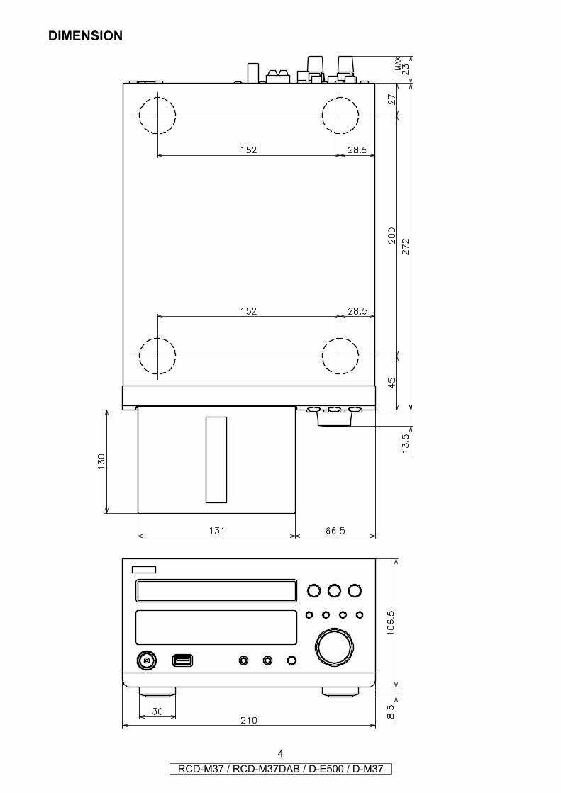
DIMENSION

5RCD-M37 / RCD-M37DAB / D-E500 / D-M37
ワイヤー整形図調整や部品の交換等により、ワイヤー類の結束をはずしたり移動させた場合には、それらの作業が完了した時点でワイヤーの整形をおこなってください。正しく整形されていないとノイズ発生の原因となることがあります。
上面からみたワイヤー整形
WIRE ARRANGEMENTIf wire bundles are untied or moved to perform adjustment or parts replacement etc., be sure to rearrange them neatly asthey were originally bundled or placed afterward.Otherwise, incorrect arrangement can be a cause of noisegeneration.
Wire arrangement viewed from the top
Back Panel side
Front Panel side
6RCD-M37 / RCD-M37DAB / D-E500 / D-M37
サービス時の注意事項
本機の初期化についてマイコンやマイコン周辺部品を交換した場合は、本機の初期化を行って下さい。
1. 電源ボタンを押してスタンバイ状態にしてから、壁の電源コンセントから電源コードを抜きます。
2. 8 / - ボタンとMENU/SET ボタンを同時に押しながら、電源プラグをコンセントに差し込みます。
*マイコンが初期化されます。
注意 : 初期化を行うとお客様が設定した内容が工場出荷状態に戻りますので、あらかじめ設定内容を控えておき初期化後再設定してください。
CAUTION IN SERVICING
Initializing RCD-M37DAB/RCD-M33/D-M37/D-E500RCD-M35DAB/M33 initialization should be performed when the µcom, and peripheral parts of µcom are replaced.
1. Switch off the unit and remove the AC cord from the wall outlet.
2. Hold the following 8 / - button and MENU/SET button, and plug the AC cord into the outlet.
Note: All user settings will be lost and this factory setting will be recovered when this initialization mode.So make sure to memorize your setting for restor-ing after the initialization.
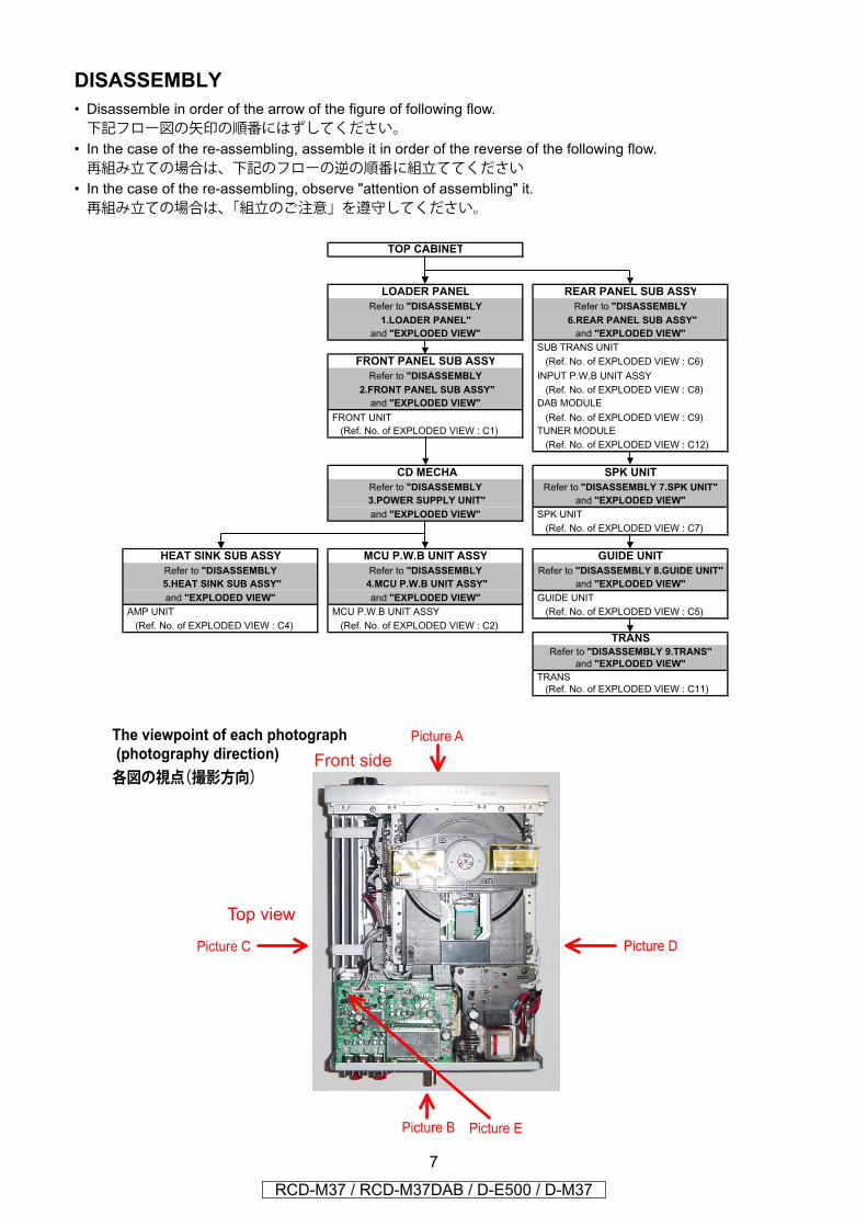
DISASSEMBLY• Disassemble in order of the arrow of the figure of following flow.下記フロー図の矢印の順番にはずしてください。
• In the case of the re-assembling, assemble it in order of the reverse of the following flow.再組み立ての場合は、下記のフローの逆の順番に組立ててください
• In the case of the re-assembling, observe "attention of assembling" it.再組み立ての場合は、「組立のご注意」を遵守してください。
TOP CABINET
LOADER PANEL REAR PANEL SUB ASSY
Refer to "DISASSEMBLY Refer to "DISASSEMBLY
1.LOADER PANEL" 6.REAR PANEL SUB ASSY"
and "EXPLODED VIEW" and "EXPLODED VIEW"
SUB TRANS UNITFRONT PANEL SUB ASSY (Ref. No. of EXPLODED VIEW : C6)
Refer to "DISASSEMBLY INPUT P.W.B UNIT ASSY 2.FRONT PANEL SUB ASSY" (Ref. No. of EXPLODED VIEW : C8)
and "EXPLODED VIEW" DAB MODULE
FRONT UNIT (Ref. No. of EXPLODED VIEW : C9) (Ref. No. of EXPLODED VIEW : C1) TUNER MODULE
(Ref. No. of EXPLODED VIEW : C12)
CD MECHA SPK UNIT
Refer to "DISASSEMBLY Refer to "DISASSEMBLY 7.SPK UNIT"
3.POWER SUPPLY UNIT" and "EXPLODED VIEW"
and "EXPLODED VIEW" SPK UNIT (Ref. No. of EXPLODED VIEW : C7)
HEAT SINK SUB ASSY MCU P.W.B UNIT ASSY GUIDE UNIT
Refer to "DISASSEMBLY Refer to "DISASSEMBLY Refer to "DISASSEMBLY 8.GUIDE UNIT"
5.HEAT SINK SUB ASSY" 4.MCU P.W.B UNIT ASSY" and "EXPLODED VIEW"
and "EXPLODED VIEW" and "EXPLODED VIEW" GUIDE UNIT AMP UNIT MCU P.W.B UNIT ASSY (Ref. No. of EXPLODED VIEW : C5) (Ref. No. of EXPLODED VIEW : C4) (Ref. No. of EXPLODED VIEW : C2)
TRANS
Refer to "DISASSEMBLY 9.TRANS"
and "EXPLODED VIEW"
TRANS (Ref. No. of EXPLODED VIEW : C11)
Front side
Picture B Picture E
Picture A
Picture C Picture D
Top view
The viewpoint of each photograph
(photography direction)
各図の視点(撮影方向)
7
RCD-M37 / RCD-M37DAB / D-E500 / D-M37
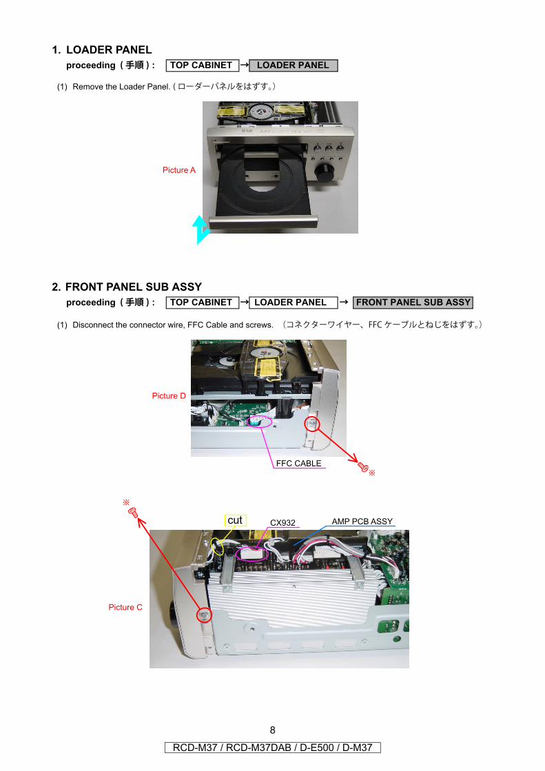
1. LOADER PANEL
(1) Remove the Loader Panel. ( ローダーパネルをはずす。)
2. FRONT PANEL SUB ASSY
(1) Disconnect the connector wire, FFC Cable and screws. (コネクターワイヤー、FFC ケーブルとねじをはずす。)
proceeding ( 手順 ) : TOP CABINET → LOADER PANEL
Picture A
proceeding ( 手順 ) : TOP CABINET → LOADER PANEL → FRONT PANEL SUB ASSY
FFC CABLE
Picture D
CX932
Picture C
AMP PCB ASSYcut
8
RCD-M37 / RCD-M37DAB / D-E500 / D-M37
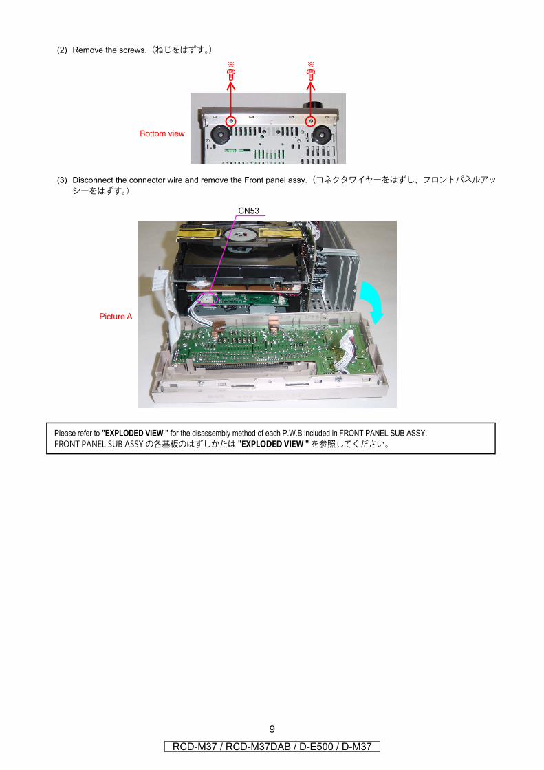
(2) Remove the screws.(ねじをはずす。)
(3) Disconnect the connector wire and remove the Front panel assy.(コネクタワイヤーをはずし、フロントパネルアッシーをはずす。)
Please refer to "EXPLODED VIEW " for the disassembly method of each P.W.B included in FRONT PANEL SUB ASSY.FRONT PANEL SUB ASSY の各基板のはずしかたは "EXPLODED VIEW "を参照してください。
Bottom view
CN53
Picture A
9
RCD-M37 / RCD-M37DAB / D-E500 / D-M37
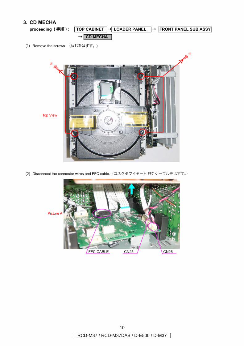
3. CD MECHA
(1) Remove the screws. (ねじをはずす。)
(2) Disconnect the connector wires and FFC cable.(コネクタワイヤーと FFC ケーブルをはずす。)
proceeding ( 手順 ) : TOP CABINET → LOADER PANEL → FRONT PANEL SUB ASSY
→ CD MECHA
Top View
CN26CN25FFC CABLE
Picture A
10
RCD-M37 / RCD-M37DAB / D-E500 / D-M37
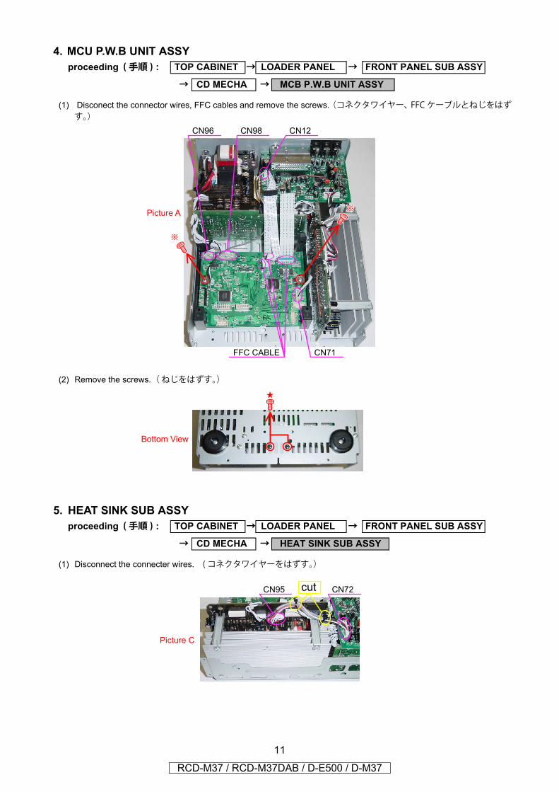
4. MCU P.W.B UNIT ASSY
(1) Disconect the connector wires, FFC cables and remove the screws.(コネクタワイヤー、FFC ケーブルとねじをはずす。)
(2) Remove the screws.( ねじをはずす。)
5. HEAT SINK SUB ASSY
(1) Disconnect the connecter wires. ( コネクタワイヤーをはずす。)
proceeding ( 手順 ) : TOP CABINET → LOADER PANEL → FRONT PANEL SUB ASSY
→ CD MECHA → MCB P.W.B UNIT ASSY
CN71
CN12CN96 CN98
FFC CABLE
Picture A
Bottom View
proceeding ( 手順 ) : TOP CABINET → LOADER PANEL → FRONT PANEL SUB ASSY
→ CD MECHA → HEAT SINK SUB ASSY
CN95 CN72cut
Picture C
11
RCD-M37 / RCD-M37DAB / D-E500 / D-M37
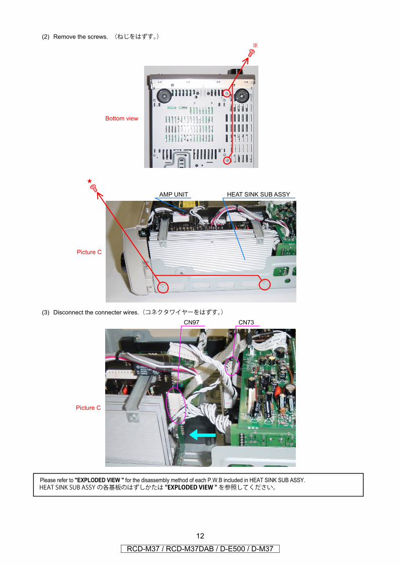
(2) Remove the screws. (ねじをはずす。)
(3) Disconnect the connecter wires.(コネクタワイヤーをはずす。)
Please refer to "EXPLODED VIEW " for the disassembly method of each P.W.B included in HEAT SINK SUB ASSY. HEAT SINK SUB ASSY の各基板のはずしかたは "EXPLODED VIEW "を参照してください。
Bottom view
Picture C
AMP UNIT HEAT SINK SUB ASSY
CN97
Picture C
CN73
12
RCD-M37 / RCD-M37DAB / D-E500 / D-M37
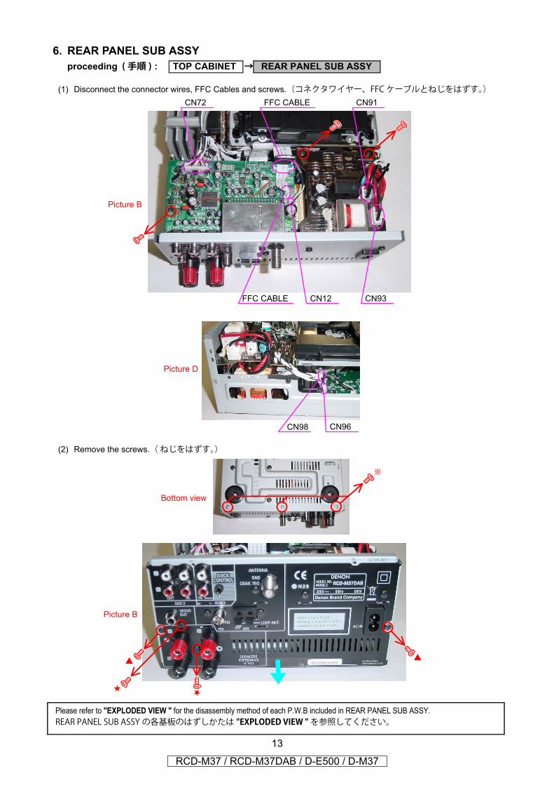
6. REAR PANEL SUB ASSY
(1) Disconnect the connector wires, FFC Cables and screws.(コネクタワイヤー、FFC ケーブルとねじをはずす。)
(2) Remove the screws.( ねじをはずす。)
Please refer to "EXPLODED VIEW " for the disassembly method of each P.W.B included in REAR PANEL SUB ASSY.REAR PANEL SUB ASSY の各基板のはずしかたは "EXPLODED VIEW "を参照してください。
proceeding ( 手順 ) : TOP CABINET → REAR PANEL SUB ASSY
CN72 FFC CABLE CN91
CN93CN12FFC CABLE
Picture B
CN96CN98
Picture D
Bottom view
Picture B
13
RCD-M37 / RCD-M37DAB / D-E500 / D-M37
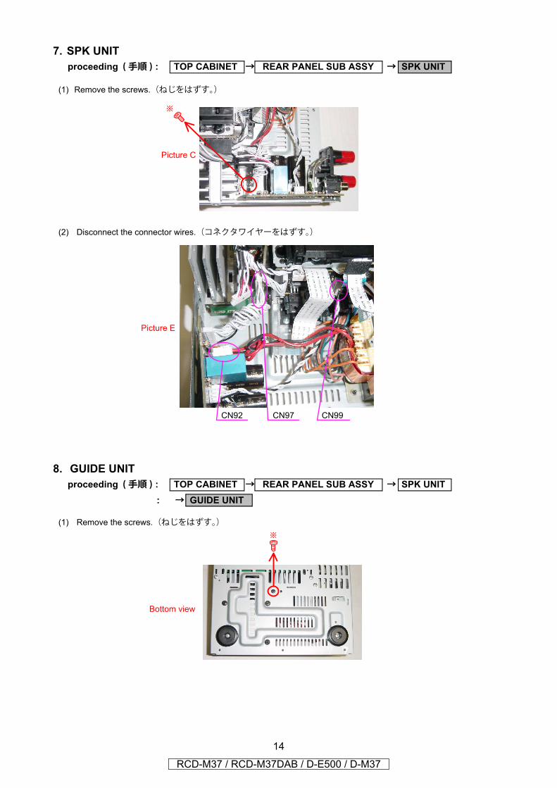
7. SPK UNIT
(1) Remove the screws.(ねじをはずす。)
(2) Disconnect the connector wires.(コネクタワイヤーをはずす。)
8. GUIDE UNIT
(1) Remove the screws.(ねじをはずす。)
proceeding ( 手順 ) : TOP CABINET → REAR PANEL SUB ASSY → SPK UNIT
Picture C
CN92 CN97 CN99
Picture E
proceeding ( 手順 ) : TOP CABINET → REAR PANEL SUB ASSY → SPK UNIT: → GUIDE UNIT
Bottom view
14
RCD-M37 / RCD-M37DAB / D-E500 / D-M37
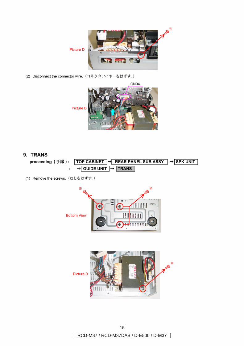
(2) Disconnect the connector wire.(コネクタワイヤーをはずす。)
9. TRANS
(1) Remove the screws.(ねじをはずす。)
Picture D
CN94
Picture B
proceeding ( 手順 ) : TOP CABINET → REAR PANEL SUB ASSY → SPK UNIT: → GUIDE UNIT → TRANS
Bottom View
Picture B
15
RCD-M37 / RCD-M37DAB / D-E500 / D-M37
16RCD-M37 / RCD-M37DAB / D-E500 / D-M37
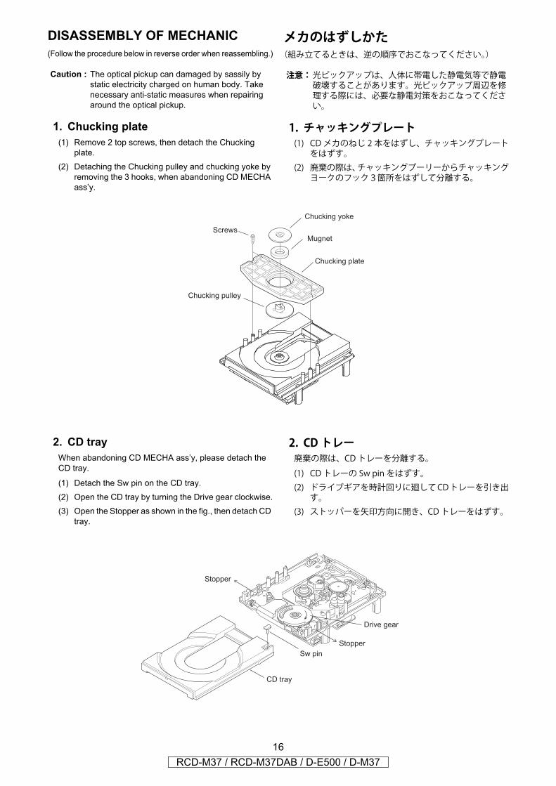
メカのはずしかた(組み立てるときは、逆の順序でおこなってください。)
注意:光ピックアップは、人体に帯電した静電気等で静電破壊することがあります。光ピックアップ周辺を修理する際には、必要な静電対策をおこなってください。
1. チャッキングプレート(1) CD メカのねじ 2本をはずし、チャッキングプレートをはずす。
(2) 廃棄の際は、チャッキングプーリーからチャッキングヨークのフック3箇所をはずして分離する。
2. CD トレー廃棄の際は、CDトレーを分離する。
(1) CD トレーの Sw pin をはずす。
(2) ドライブギアを時計回りに廻してCDトレーを引き出す。
(3) ストッパーを矢印方向に開き、CDトレーをはずす。
DISASSEMBLY OF MECHANIC(Follow the procedure below in reverse order when reassembling.)
Caution : The optical pickup can damaged by sassily by static electricity charged on human body. Take necessary anti-static measures when repairing around the optical pickup.
1. Chucking plate(1) Remove 2 top screws, then detach the Chucking
plate.
(2) Detaching the Chucking pulley and chucking yoke by removing the 3 hooks, when abandoning CD MECHA ass’y.
2. CD trayWhen abandoning CD MECHA ass’y, please detach the CD tray.
(1) Detach the Sw pin on the CD tray.
(2) Open the CD tray by turning the Drive gear clockwise.
(3) Open the Stopper as shown in the fig., then detach CD tray.
Chucking yoke
Chucking plate
Chucking pulley
Screws
Mugnet
Stopper
Stopper
Sw pin
CD tray
Drive gear
�
17RCD-M37 / RCD-M37DAB / D-E500 / D-M37
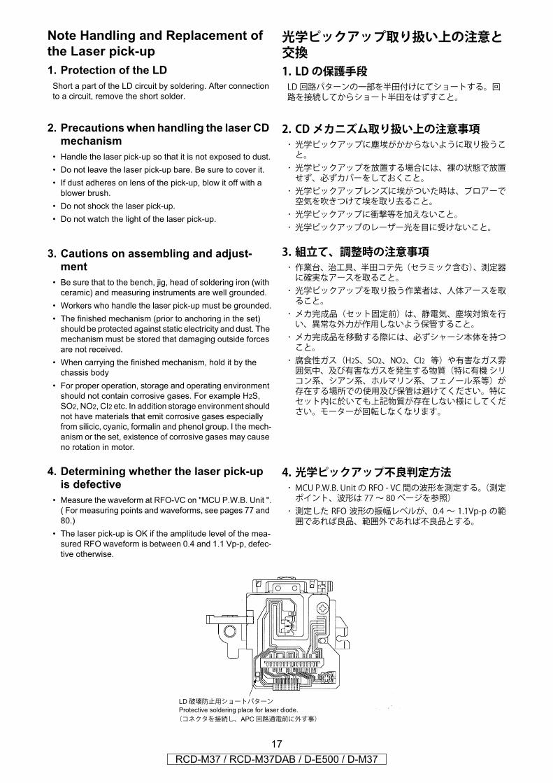
Note Handling and Replacement of the Laser pick-up1. Protection of the LD
Short a part of the LD circuit by soldering. After connection to a circuit, remove the short solder.
2. Precautions when handling the laser CD mechanism
• Handle the laser pick-up so that it is not exposed to dust.• Do not leave the laser pick-up bare. Be sure to cover it.• If dust adheres on lens of the pick-up, blow it off with a
blower brush.• Do not shock the laser pick-up.• Do not watch the light of the laser pick-up.
3. Cautions on assembling and adjust-ment
• Be sure that to the bench, jig, head of soldering iron (with ceramic) and measuring instruments are well grounded.
• Workers who handle the laser pick-up must be grounded.• The finished mechanism (prior to anchoring in the set)
should be protected against static electricity and dust. The mechanism must be stored that damaging outside forces are not received.
• When carrying the finished mechanism, hold it by the chassis body
• For proper operation, storage and operating environment should not contain corrosive gases. For example H2S, SO2, NO2, CI2 etc. In addition storage environment should not have materials that emit corrosive gases especially from silicic, cyanic, formalin and phenol group. I the mech-anism or the set, existence of corrosive gases may cause no rotation in motor.
4. Determining whether the laser pick-up is defective
• Measure the waveform at RFO-VC on "MCU P.W.B. Unit ".( For measuring points and waveforms, see pages 77 and 80.)
• The laser pick-up is OK if the amplitude level of the mea-sured RFO waveform is between 0.4 and 1.1 Vp-p, defec-tive otherwise.
LD破壊防止用ショートパターンProtective soldering place for laser diode.(コネクタを接続し、APC回路通電前に外す事)
光学ピックアップ取り扱い上の注意と交換1. LD の保護手段LD 回路パターンの一部を半田付けにてショートする。回路を接続してからショート半田をはずすこと。
2. CD メカニズム取り扱い上の注意事項・ 光学ピックアップに塵埃がかからないように取り扱うこと。・ 光学ピックアップを放置する場合には、裸の状態で放置せず、必ずカバーをしておくこと。・ 光学ピックアップレンズに埃がついた時は、ブロアーで空気を吹きつけて埃を取り去ること。・ 光学ピックアップに衝撃等を加えないこと。・ 光学ピックアップのレーザー光を目に受けないこと。
3. 組立て、調整時の注意事項・ 作業台、治工具、半田コテ先(セラミック含む)、測定器に確実なアースを取ること。・ 光学ピックアップを取り扱う作業者は、人体アースを取ること。・ メカ完成品(セット固定前)は、静電気、塵埃対策を行い、異常な外力が作用しないよう保管すること。・ メカ完成品を移動する際には、必ずシャーシ本体を持つこと。・ 腐食性ガス(H2S、SO2、NO2、CI2 等)や有害なガス雰囲気中、及び有害なガスを発生する物質(特に有機 シリコン系、シアン系、ホルマリン系、フェノール系等)が存在する場所での使用及び保管は避けてください。特にセット内に於いても上記物質が存在しない様にしてください。モーターが回転しなくなります。
4. 光学ピックアップ不良判定方法・ MCU P.W.B. Unit の RFO - VC 間の波形を測定する。(測定ポイント、波形は 77 ~ 80 ページを参照)・ 測定した RFO 波形の振幅レベルが、0.4 ~ 1.1Vp-p の範囲であれば良品、範囲外であれば不良品とする。
CD TEST MODENo Key name Function Display
1Version No. of Main MPU Dis-play Mode
S1・Plug AC cord into power outlet while pressing
ON/STANDBY Key and SDB/TONE Key sametime on Main Unit.
・The Version number of Main MPU is displayed.・Unplug AC cord to clear this mode.
・Upper : "_ _ _ _ Ver _ * * * * _ _ _ _" "****" is the Version number of Main MPU
・Lower : "_ _ _ _ _ _ _ _ _ _ _ _ _ _ _ _"
2FLD(VFD) check-ing mode
S2・Plug AC cord into power outlet while pressing
ON/STANDBY Key and OPEN/CLOSE Keysame time on Main Unit.
・All segment of FLD is turning on and off everyone second.
・Unplug AC cord to clear this mode.
・All segment turn on and off.
3 CD service mode
・Plug AC cord into power outlet while pressingON/STANDBY Key and FUNCTION Key sametime on Main Unit.
・Move the slide to the initially set position (10 mmtowards the outside from the innermost position).
・Check by performing key input. Refer to 3.1 to3.6.
・Cancel the mode by turning the power back on. ・Input of keys other than those used in this mode
is not guaranteed. (OK if malfunction occurs)
・ flashing ・Upper : "_ 00 _ CD_Ver _ * * * * _" displayed
**** : CD microprocessor version no. ・Lower : "_ _ _ _ _ _ _ _ _ _ _ _ _ _ _ _"
3.1 Disc loading
・Press the CD OPEN/CLOSE key to open the tray. ・Set a disc on the tray, then press the CD OPEN/
CLOSE key again to close the tray. The disc ismounted automatically.
・Move the slide to the initially set position (10 mmtowards the outside from the innermost position)and stop in this status.
Continue S6 display
1RCD-M37 / RCD-M37
CD テストモードNo キー名称 機能 表記
1メインマイコン バージョン表示モード
S1・本体 ON/STANDBY キーと SDB/TONE キーを同時に押しながら、AC コードをコンセントへ接続する .
・メインマイコンの Ver を表示する.MUTING ON.・AC コードを抜くことによりモードを解除する.
・上段:"_ _ _ _ Ver _ * * * * _ _ _ _" 表示****:メインマイコンの Ver 番号
・下段:"_ _ _ _ _ _ _ _ _ _ _ _ _ _ _ _"
2FL(VFD) 管チェックモード
S2・本体 ON/STANDBY キーと CD OPEN/CLOSE キーを同時に押しながら、AC コードをコンセントへ接続する.
・FL 管の全てを 2秒周期で点滅 (1 秒点灯、1秒消灯 ) する.MUTING ON.
・AC コードを抜くことによりモードを解除する.
・全てのセグメントを点灯・消灯する.
3 CD サービスモード
・本体ON/STANDBY キーと FUNCTION キーを同時に押しながら、AC コードをコンセントへ接続する.
・スライドを初期設定位置に移動する.(最内周から外側 10mmの位置)
・キー入力によりチェックを行う. 3.1 ~ 3.6 参照.・電源の再投入によりモードを解除する.・このモードで使用するキー以外の入力は保証しない.(異常な動作になってもよしとする)
・ を点滅・上段:"_ 00 _ CD_Ver _ * * * * _" 表示****:CD マイコンの Ver 番号
・下段:"_ _ _ _ _ _ _ _ _ _ _ _ _ _ _ _"
3.1 ディスク装着
・CD OPEN/CLOSE キーでトレイを開く.・ディスクを置き、再度 CD OPEN/CLOSE キーでトレイを閉じるとディスクをチャッキングする.
・スライドを初期設定位置(最内周から外側10mmの位置)に移動し、その状態でストップする.
S6 の表示を継続する.
8DAB / D-E500 / D-M37
3.2 Servo check
・Press the CD PLAY/PAUSE key. Execute thefollowing steps. ① LD ON (with servo still stopped)② FOCUS ON (disc rotation, tracking off)
If no disc loaded, retry then stop. ③ CLV ON④ TRACKING ON⑤ SUB CODE readout (playback sound output) ⑥ When display is as in ⑤ and the PLAY button
is pressed, conduct BER (Block Error Rate)display for 2 seconds. (Display total no.generated in 10 seconds.)
* Press PLAY button continuously for over 1second to switch directly to SUB CODEreadout in step ⑤ .
・ flashing ①・Upper : " 01 _ _ _ _ __ LD_ON _" displayed・Lower : "_ _ _ _ _ _ _ _ _ _ _ _ _ _ _ _"
②・Upper : " _ 02 _ _ _ _ Focus_ON _" displayed
③・Upper : "_ 03 _ _ _ _ _ _ CLV_ON _" displayed
④・Upper : "_ 04 _ Tracking_ON _" displayed
⑤・Upper : "_ 05 _ _ _ @@Tr _ _ XX:XX" displayed@@ : T.NoXX:XX : Time
⑥・Upper : "_ _ _ _ _ _ ERR _ ######" displayed###### : B.E.R.
3.3 Pickup movement
・In the stop mode, pickup moves in REV (inwards)or FWD (outwards) direction when keyor key pressed.
・When key pressed, move to stopoperation after detection that inner switch hasturned on.
・Pickup movement stops when key released.(Pickup moves while key is pressed.)
Continuous display of previous time
3.4 Stop・When STOP key is pressed, play operation and
servo stop. ・After stopping, conduct reading of auto adjust values.
・Same as 3.
3.5 All servo on
・When MENU/SET key is pressed, all servos turnon, auto adjustment is performed and switch toplayback operation. (Playback sound output)
・ flashing ・Upper : "_ _ _ _ _ _ @@Tr _ _ XX:XX" displayed
@@ : T.NoXX:XX : Time
・Lower : "_ _ _ _ _ _ _ _ _ _ _ _ _ _ _ _"
No Key name Function Display
1RCD-M37 / RCD-M37
3.2 サーボチェック
・CD PLAY/PAUSE キーを押すと下記ステップを実行する.① LD ON( サーボ停止のまま )② FOCUS ON( ディスク回転、トラッキング OFF)ディスク無しの場合、リトライ後停止する.
③ CLV ON④ TRACKING ON⑤ SUB CODE 読み出し(再生音出力)⑥ ⑤の表示時に PLAY ボタンを押すと、2秒間BER(Block Error Rate) の表示を行なう.(10 秒間の間に発生した総数を表示)
* PLAY ボタンの 1 秒以上押し続けにて、ダイレクトに⑤の SUB CODE 読み出しステップに移行する.
・ を点滅①・上段:" 01 _ _ _ _ __ LD_ON _" 表示・下段:"_ _ _ _ _ _ _ _ _ _ _ _ _ _ _ _"
②・上段:" _ 02 _ _ _ _ Focus_ON _" 表示
③・上段:"_ 03 _ _ _ _ _ _ CLV_ON _" 表示
④・上段:"_ 04 _ Tracking_ON _" 表示
⑤・上段:"_ 05 _ _ _ @@Tr _ _ XX:XX" 表示 @@:T.No XX:XX:時間
⑥・上段:"_ _ _ _ _ _ ERR _ ######" 表示 ######:B.E.R.
3.3 ピックアップ移動
・ストップ状態で キーまたは キーを押すと、ピックアップが REV( 内周側 ) または FWD( 外周側 ) 方向に移動する.
・ キーを押した時は、内周 SWのONを検出後ストップ動作に移行する.
・キーを離すとピックアップの移動を停止する.( キーが押されている間、移動する.)
前回の表示を継続する.
3.4 停止・STOP キーを押すと、PLAY 動作及びサーボを停止する.
・停止後、自動調整値の読込みを行なう.
・3と同じ.
3.5 全サーボ ON
・MENU/SET キーを押すと全サーボを ONし、自動調整を行なって再生動作に移行する.(再生音出力)
・ を点滅・上段:"_ _ _ _ _ _ @@Tr _ _ XX:XX" 表示 @@:T.No XX:XX:時間・下段:"_ _ _ _ _ _ _ _ _ _ _ _ _ _ _ _"
No キー名称 機能 表記
9DAB / D-E500 / D-M37

3.6Adjustment value display
・When SDB/TONE key is pressed, the adjustmentvalues are displayed in the following order. ① FOCUS BALANCE② FOCUS GAIN③ TRACKING BALANCE④ TRACKING GAIN⑤ FOCUS OFFSET⑥ TRACKING OFFSET⑦ RFRP⑧ Return to ① .
(NOTE) If auto adjustment is not completed,proper values are not displayed.
・ flashing ①・Upper : "FOCUS _ BALANCE _ _ _"・Lower : "XX _ _ _ _ _ _ _ _ _ _ _ _ _ _"・XX : Adjustment value
②・Upper : "FOCUS _ GAIN _ _ _ _ _ _"・Lower : "XX _ _ _ _ _ _ _ _ _ _ _ _ _ _"・XX : Adjustment value
③・Upper : "TRACKING _ BALANCE"・Lower : "XX _ _ _ _ _ _ _ _ _ _ _ _ _ _"・XX : Adjustment value
④・Upper : "TRACKING _ GAIN _ _ _"・Lower : "XX _ _ _ _ _ _ _ _ _ _ _ _ _ _"・XX : Adjustment value
⑤・Upper : "FOCUS _ OFFSET _ _ _ _"・Lower : "XX _ _ _ _ _ _ _ _ _ _ _ _ _ _"・XX : Adjustment value
⑥・Upper : "TRACKING _ OFFSET _"・Lower : "XX _ _ _ _ _ _ _ _ _ _ _ _ _ _"・XX : Adjustment value
⑦・Upper : "RFRP _ _ _ _ _ _ _ _ _ _ _ _"・Lower : "XX _ _ _ _ _ _ _ _ _ _ _ _ _ _"・XX : Adjustment value
No Key name Function Display
2RCD-M37 / RCD-M37
3.6 調整値の表示
・SDB/TONE キーを押すと、下記の順番で調整値を表示する.① FOCUS BALANCE② FOCUS GAIN③ TRACKING BALANCE④ TRACKING GAIN⑤ FOCUS OFFSET⑥ TRACKING OFFSET⑦ RFRP⑧ ①に戻る。( 注 ) 自動調整を終了して無い場合は正常な値が
表示されない.
・ を点滅①・上段:"FOCUS _ BALANCE _ _ _"・下段:"XX _ _ _ _ _ _ _ _ _ _ _ _ _ _"・XX:調整値
②・上段:"FOCUS _ GAIN _ _ _ _ _ _"・下段:"XX _ _ _ _ _ _ _ _ _ _ _ _ _ _"・XX:調整値
③・上段:"TRACKING _ BALANCE"・下段:"XX _ _ _ _ _ _ _ _ _ _ _ _ _ _"・XX:調整値
④・上段:"TRACKING _ GAIN _ _ _"・下段:"XX _ _ _ _ _ _ _ _ _ _ _ _ _ _"・XX:調整値
⑤・上段:"FOCUS _ OFFSET _ _ _ _"・下段:"XX _ _ _ _ _ _ _ _ _ _ _ _ _ _"・XX:調整値
⑥・上段:"TRACKING _ OFFSET _"・下段:"XX _ _ _ _ _ _ _ _ _ _ _ _ _ _"・XX:調整値
⑦・上段:"RFRP _ _ _ _ _ _ _ _ _ _ _ _"・下段:"XX _ _ _ _ _ _ _ _ _ _ _ _ _ _"・XX:調整値
No キー名称 機能 表記
0DAB / D-E500 / D-M37
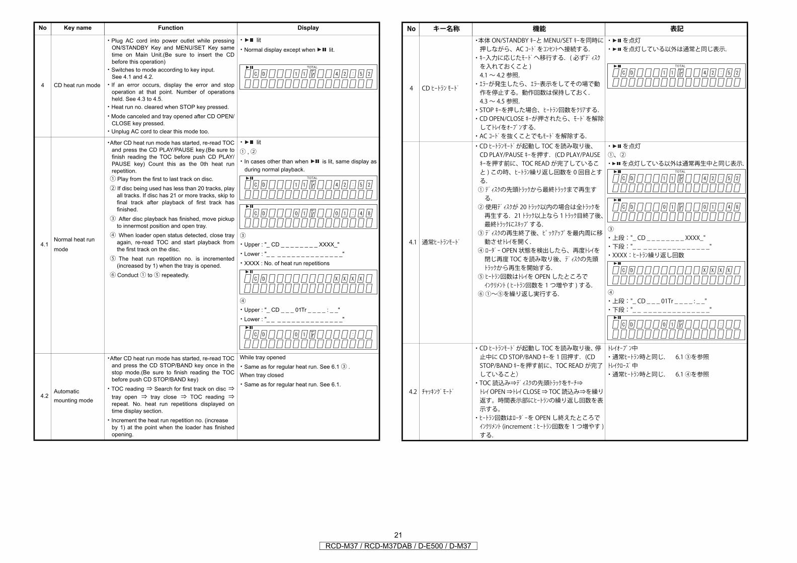
4 CD heat run mode
・Plug AC cord into power outlet while pressingON/STANDBY Key and MENU/SET Key sametime on Main Unit.(Be sure to insert the CDbefore this operation)
・Switches to mode according to key input. See 4.1 and 4.2.
・If an error occurs, display the error and stopoperation at that point. Number of operationsheld. See 4.3 to 4.5.
・Heat run no. cleared when STOP key pressed. ・Mode canceled and tray opened after CD OPEN/
CLOSE key pressed. ・Unplug AC cord to clear this mode too.
・ lit・Normal display except when lit.
4.1Normal heat run
mode
・After CD heat run mode has started, re-read TOCand press the CD PLAY/PAUSE key.(Be sure tofinish reading the TOC before push CD PLAY/PAUSE key) Count this as the 0th heat runrepetition.① Play from the first to last track on disc.② If disc being used has less than 20 tracks, play
all tracks. If disc has 21 or more tracks, skip tofinal track after playback of first track hasfinished.
③ After disc playback has finished, move pickupto innermost position and open tray.
④ When loader open status detected, close trayagain, re-read TOC and start playback fromthe first track on the disc.
⑤ The heat run repetition no. is incremented(increased by 1) when the tray is opened.
⑥ Conduct ① to ⑤ repeatedly.
・ lit① ,②・In cases other than when is lit, same display as
during normal playback.
③・Upper : "_ CD _ _ _ _ _ _ _ _ XXXX_"・Lower : "_ _ _ _ _ _ _ _ _ _ _ _ _ _ _ _"・XXXX : No. of heat run repetitions
④・Upper : "_ CD _ _ _ 01Tr _ _ _ _ : _ _"・Lower : "_ _ _ _ _ _ _ _ _ _ _ _ _ _ _ _"
4.2Automatic mounting mode
・After CD heat run mode has started, re-read TOCand press the CD STOP/BAND key once in thestop mode.(Be sure to finish reading the TOCbefore push CD STOP/BAND key)
・TOC reading ⇒ Search for first track on disc ⇒tray open ⇒ tray close ⇒ TOC reading ⇒repeat. No. heat run repetitions displayed ontime display section.
・Increment the heat run repetition no. (increase by 1) at the point when the loader has finishedopening.
While tray opened・Same as for regular heat run. See 6.1 ③ .When tray closed・Same as for regular heat run. See 6.1.
No Key name Function Display
2RCD-M37 / RCD-M37
4 CD ヒートラン モード
・本体 ON/STANDBY キーと MENU/SET キーを同時に押しながら、AC コードをコンセントへ接続する.
・キー入力に応じたモードへ移行する.( 必ずディスクを入れておくこと )4.1 ~ 4.2 参照.
・エラーが発生したら、エラー表示をしてその場で動作を停止する。動作回数は保持しておく.4.3 ~ 4.5 参照.
・STOP キーを押した場合、ヒートラン回数をクリアする.・CD OPEN/CLOSE キーが押されたら、モードを解除してトレイをオープンする.
・AC コードを抜くことでもモードを解除する.
・ を点灯・ を点灯している以外は通常と同じ表示.
4.1 通常ヒートランモード
・CD ヒートランモードが起動し TOCを読み取り後、CD PLAY/PAUSE キーを押す.(CD PLAY/PAUSE キーを押す前に、TOC READ が完了していること ) この時、ヒートラン繰り返し回数を 0回目とする.① ディスクの先頭トラックから最終トラックまで再生する.
② 使用ディスクが 20 トラック以内の場合は全トラックを再生する.21 トラック以上なら1トラック目終了後、最終トラックにスキップする.
③ ディスクの再生終了後、ピックアップを最内周に移動させトレイを開く.
④ ローダー OPEN 状態を検出したら、再度トレイを閉じ再度 TOCを読み取り後、ディスクの先頭トラックから再生を開始する.
⑤ ヒートラン回数はトレイを OPEN したところでインクリメント ( ヒートラン回数を 1つ増やす ) する.
⑥ ①~⑤を繰り返し実行する.
・ を点灯①、②・ を点灯している以外は通常再生中と同じ表示.
③・上段:"_ CD _ _ _ _ _ _ _ _ XXXX_"・下段:"_ _ _ _ _ _ _ _ _ _ _ _ _ _ _ _"・XXXX:ヒートラン繰り返し回数
④・上段:"_ CD _ _ _ 01Tr _ _ _ _ : _ _"・下段:"_ _ _ _ _ _ _ _ _ _ _ _ _ _ _ _"
4.2 チャッキングモード
・CD ヒートランモードが起動し TOCを読み取り後、 停止中に CD STOP/BAND キーを 1回押す.(CD STOP/BAND キーを押す前に、TOC READ が完了していること)
・TOC読込み⇒ディスクの先頭トラックをサーチ⇒トレイ OPEN⇒トレイ CLOSE⇒ TOC読込み⇒を繰り返す。時間表示部にヒートランの繰り返し回数を表示する。
・ヒートラン回数はローダーを OPENし終えたところでインクリメント (increment:ヒートラン回数を 1つ増やす )する.
トレイオープン中・通常ヒートラン時と同じ. 6.1 ③を参照トレイクローズ中・通常ヒートラン時と同じ. 6.1 ④を参照
No キー名称 機能 表記
1DAB / D-E500 / D-M37
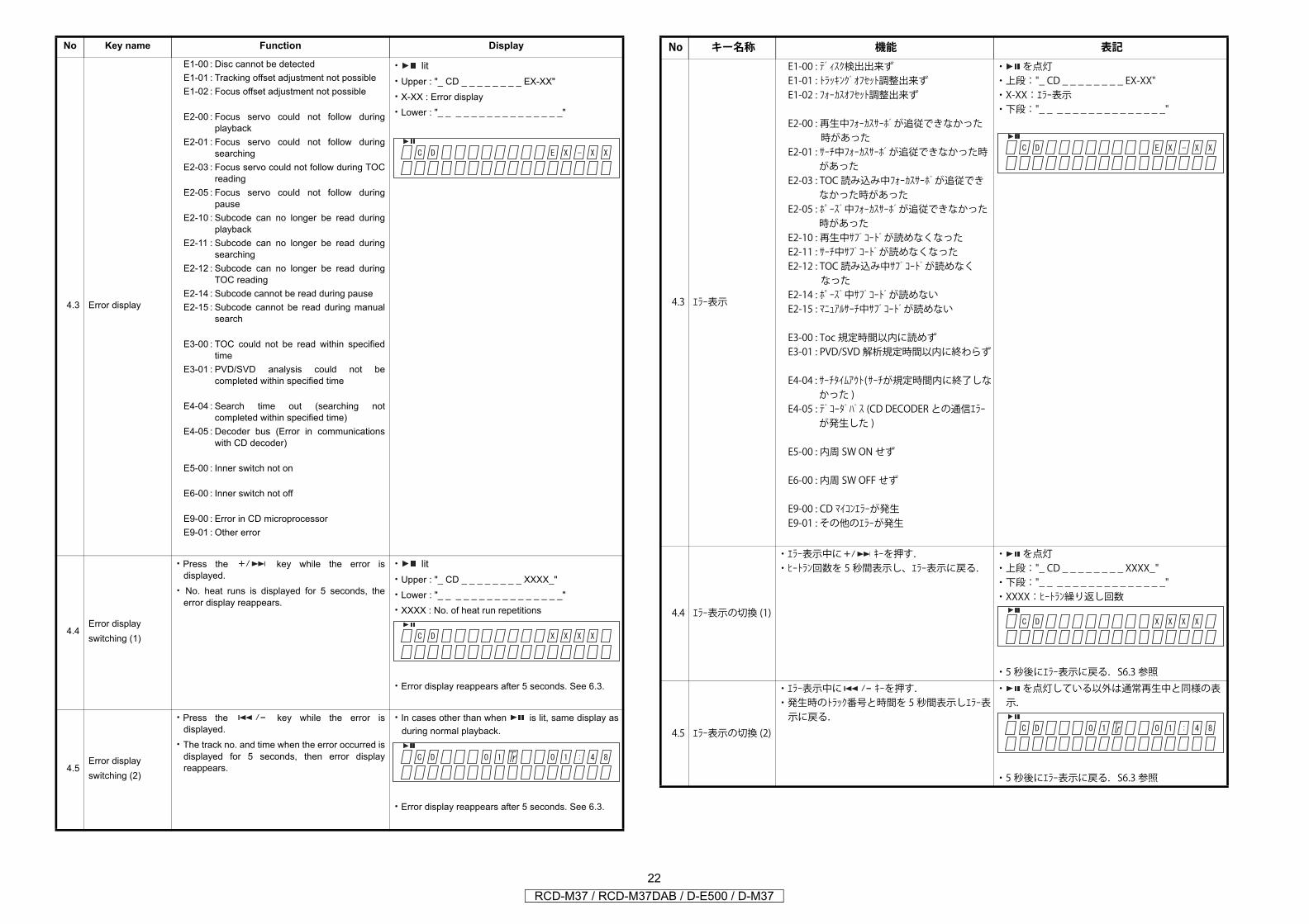
4.3 Error display
E1-00 : Disc cannot be detected E1-01 : Tracking offset adjustment not possibleE1-02 : Focus offset adjustment not possible
E2-00 : Focus servo could not follow duringplayback
E2-01 : Focus servo could not follow duringsearching
E2-03 : Focus servo could not follow during TOCreading
E2-05 : Focus servo could not follow duringpause
E2-10 : Subcode can no longer be read duringplayback
E2-11 : Subcode can no longer be read duringsearching
E2-12 : Subcode can no longer be read duringTOC reading
E2-14 : Subcode cannot be read during pauseE2-15 : Subcode cannot be read during manual
search
E3-00 : TOC could not be read within specifiedtime
E3-01 : PVD/SVD analysis could not becompleted within specified time
E4-04 : Search time out (searching notcompleted within specified time)
E4-05 : Decoder bus (Error in communicationswith CD decoder)
E5-00 : Inner switch not on
E6-00 : Inner switch not off
E9-00 : Error in CD microprocessor E9-01 : Other error
・ lit・Upper : "_ CD _ _ _ _ _ _ _ _ EX-XX"・X-XX : Error display・Lower : "_ _ _ _ _ _ _ _ _ _ _ _ _ _ _ _"
4.4Error display switching (1)
・Press the key while the error isdisplayed.
・ No. heat runs is displayed for 5 seconds, theerror display reappears.
・ lit・Upper : "_ CD _ _ _ _ _ _ _ _ XXXX_"・Lower : "_ _ _ _ _ _ _ _ _ _ _ _ _ _ _ _"・XXXX : No. of heat run repetitions
・Error display reappears after 5 seconds. See 6.3.
4.5Error display switching (2)
・Press the key while the error isdisplayed.
・ The track no. and time when the error occurred isdisplayed for 5 seconds, then error displayreappears.
・In cases other than when is lit, same display asduring normal playback.
・Error display reappears after 5 seconds. See 6.3.
No Key name Function Display
2RCD-M37 / RCD-M37
4.3 エラー表示
E1-00 : ディスク検出出来ずE1-01 : トラッキングオフセット調整出来ずE1-02 : フォーカスオフセット調整出来ず
E2-00 : 再生中フォーカスサーボが追従できなかった時があった
E2-01 : サーチ中フォーカスサーボが追従できなかった時があった
E2-03 : TOC 読み込み中フォーカスサーボが追従できなかった時があった
E2-05 : ポーズ中フォーカスサーボが追従できなかった時があった
E2-10 : 再生中サブコードが読めなくなったE2-11 : サーチ中サブコードが読めなくなったE2-12 : TOC 読み込み中サブコードが読めなく
なったE2-14 : ポーズ中サブコードが読めないE2-15 : マニュアルサーチ中サブコードが読めない
E3-00 : Toc 規定時間以内に読めずE3-01 : PVD/SVD 解析規定時間以内に終わらず
E4-04 : サーチタイムアウト(サーチが規定時間内に終了しなかった )
E4-05 : デコーダバス (CD DECODER との通信エラーが発生した )
E5-00 : 内周 SW ONせず
E6-00 : 内周 SW OFF せず
E9-00 : CD マイコンエラーが発生E9-01 : その他のエラーが発生
・ を点灯・上段:"_ CD _ _ _ _ _ _ _ _ EX-XX"・X-XX:エラー表示・下段:"_ _ _ _ _ _ _ _ _ _ _ _ _ _ _ _"
4.4 エラー表示の切換 (1)
・エラー表示中に キーを押す.・ヒートラン回数を 5秒間表示し、エラー表示に戻る.
・ を点灯・上段:"_ CD _ _ _ _ _ _ _ _ XXXX_"・下段:"_ _ _ _ _ _ _ _ _ _ _ _ _ _ _ _"・XXXX:ヒートラン繰り返し回数
・5秒後にエラー表示に戻る.S6.3 参照
4.5 エラー表示の切換 (2)
・エラー表示中に キーを押す.・発生時のトラック番号と時間を 5秒間表示しエラー表示に戻る.
・ を点灯している以外は通常再生中と同様の表示.
・5秒後にエラー表示に戻る.S6.3 参照
No キー名称 機能 表記
2DAB / D-E500 / D-M37
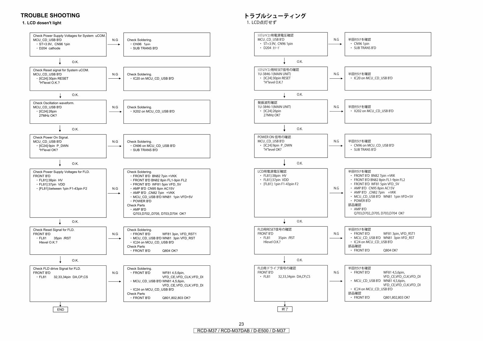
TROUBLE SHOOTING トラ ル1. LCD dosen't light 1. LCD
Check Power Supply Voltages for System uCOM.MCU_CD_USB B'D N.G Check Soldering.
ST+3.9V, CN96 1pin 96 1D204 cathode SUB TRANS B'D
O.K.
Check Reset signal for System uCOM.MCU_CD_USB B'D N.G Check Soldering.
[IC24]:30pin RESET IC20 on MCU_CD_USB B'D"H"level O.K.?
O.K.
Check Oscillation waveform.MCU_CD_USB B'D N.G Check Soldering.
[IC24]:26pin X202 on MCU_CD_USB B'D27MHz OK?
O.K.
Check Power On Signal.MCU_CD_USB B'D N.G Check Soldering.
[IC24]:9pin P_DWN CN96 on MCU_CD_USB B'D"H"level OK? SUB TRANS B'D
O.K.
Check Power Supply Voltages for FLD. Check Soldering.FRONT B'D FRONT B'D BN82 7pin +VKK
FL81]:38pin HV FRONT B'D BN82 8pin FL1-9pin FL2FL81]:37pin VDD FRONT B'D WF81 5pin VFD_5V[FL81]:between 1pin F1-43pin F2 N.G AMP B'D CN95 8pin AC15V
AMP B'D ,CN82 7pin +VKKMCU_CD_USB B'D WN81 1pin VFD+5VPOWER B'D
Check PartsAMP B'D Q703,D702,,D705, D703,D704 OK?
O.K.
Check Reset Signal for FLD. Check Soldering.FRONT B'D N.G FRONT B'D WF81 3pin, VFD_RST1
FL81 35pin /RST MCU_CD_USB B'D WN81 3pin VFD_RSTHlevel O.K.? IC24 on MCU_CD_USB B'D
Check PartsFRONT B'D Q804 OK?
O.K.
Check FLD dirive Signal for FLD. Check Soldering.FRONT B'D N.G FRONT B'D WF81 4,5,6pin,
FL81 32,33,34pin DA,CP,CS VFD_CE,VFD_CLK,VFD_DIMCU_CD_USB B'D WN81 4,5,6pin,
VFD_CE,VFD_CLK,VFD_DIIC24 on MCU_CD_USB B'D
Check PartsFRONT B'D Q801,802,803 OK?
END
2RCD-M37 / RCD-M37
シューティンせ
トラブルシューティングトラブルシューティング1. LCD点灯せず
システムマイコン用電源電圧確認MCU_CD_USB B'D N.G 半田付けを確認・ ST+3.9V, CN96 1pin ・ CN96 1pin・ D204 カソード ・ SUB TRANS B'D
O.K.
システムマイコン用RESET信号の確認1U-3846-1(MAIN UNIT) N.G 半田付けを確認・ [IC24]:30pin RESET ・ IC20 on MCU_CD_USB B'D
"H"level O.K.?
O.K.
発振波形確認1U-3846-1(MAIN UNIT) N.G 半田付けを確認・ [IC24]:26pin ・ X202 on MCU_CD_USB B'D
27MHz OK?
O.K.
POWER ON 信号の確認MCU_CD_USB B'D N.G 半田付けを確認・ [IC24]:9pin P_DWN ・ CN96 on MCU_CD_USB B'D
"H"level OK? ・ SUB TRANS B'D
O.K.
LCD用電源電圧確認 半田付けを確認・ FL81]:38pin HV ・ FRONT B'D BN82 7pin +VKK・ FL81]:37pin VDD ・ FRONT B'D BN82 8pin FL1-9pin FL2・ [FL81]: 1pin F1-43pin F2 ・ FRONT B'D WF81 5pin VFD_5V
N.G ・ AMP B'D CN95 8pin AC15V・ AMP B'D ,CN82 7pin +VKK・ MCU_CD_USB B'D WN81 1pin VFD+5V・ POWER B'D
部品確認・ AMP B'D
Q703,D702,,D705, D703,D704 OK?
O.K.
FLD用RESET信号の確認 半田付けを確認FRONT B'D N.G ・ FRONT B'D WF81 3pin, VFD_RST1・ FL81 35pin /RST ・ MCU_CD_USB B'D WN81 3pin VFD_RST
Hlevel O.K.? ・ IC24 on MCU_CD_USB B'D部品確認・ FRONT B'D Q804 OK?
O.K.
FLD用ドライブ信号の確認 半田付けを確認FRONT B'D N.G ・ FRONT B'D WF81 4,5,6pin, ・ FL81 32,33,34pin DA,CP,CS VFD_CE,VFD_CLK,VFD_DI
・ MCU_CD_USB B'D WN81 4,5,6pin, VFD_CE,VFD_CLK,VFD_DI
・ IC24 on MCU_CD_USB B'D部品確認・ FRONT B'D Q801,802,803 OK?
終了
3DAB / D-E500 / D-M37
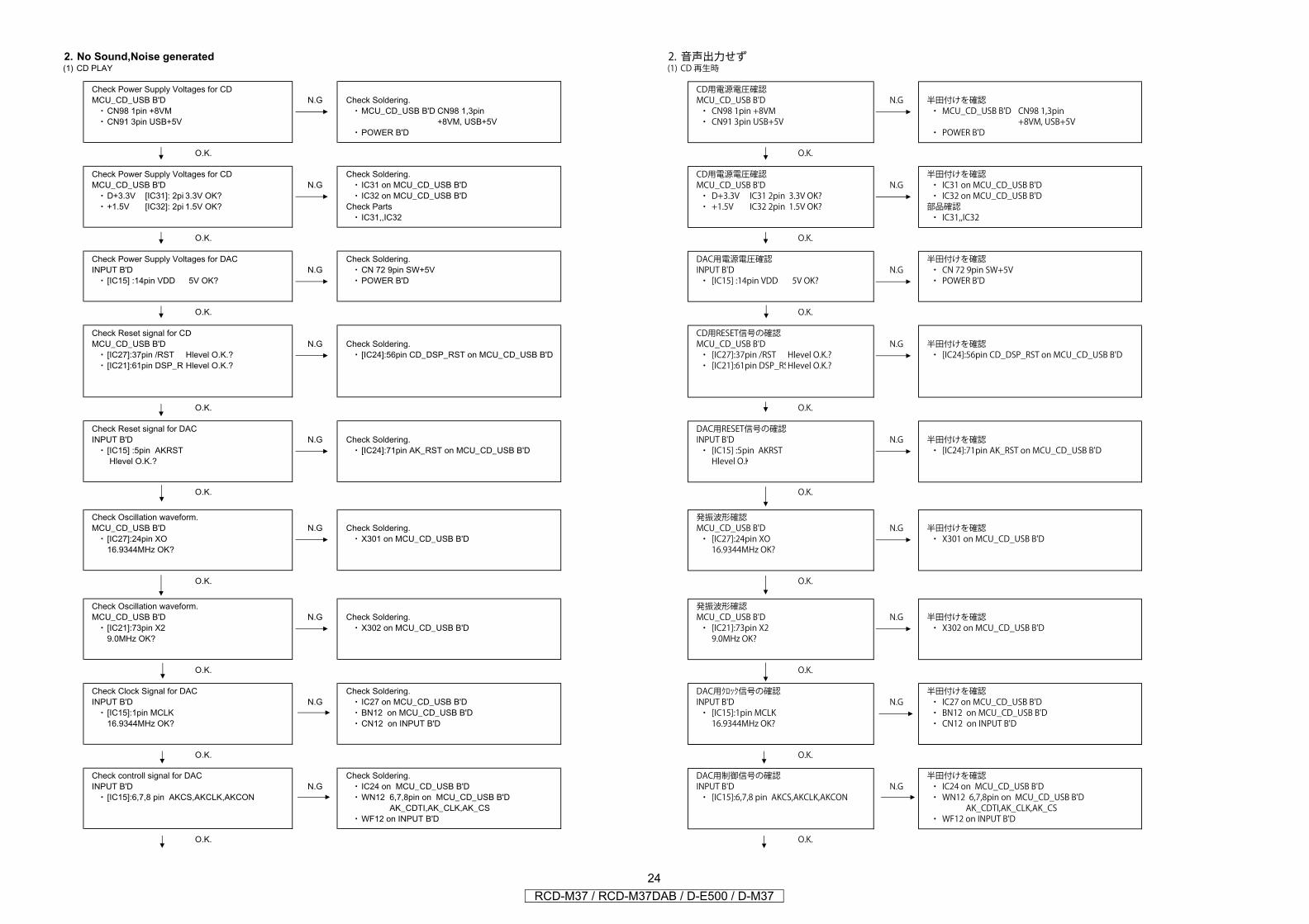
2. No Sound,Noise generated 2. 音声出(1) CD PLAY
Check Power Supply Voltages for CDMCU_CD_USB B'D N.G Check Soldering.
CN98 1pin +8VM MCU_CD_USB B'D CN98 1,3pinCN91 3pin USB+5V +8VM, USB+5V
POWER B'D
O.K.
Check Power Supply Voltages for CD Check Soldering.MCU_CD_USB B'D N.G IC31 on MCU_CD_USB B'D
D+3.3V [IC31]: 2pi 3.3V OK? IC32 on MCU_CD_USB B'D+1.5V [IC32]: 2pi 1.5V OK? Check Parts
IC31,,IC32
O.K.
Check Power Supply Voltages for DAC Check Soldering.INPUT B'D N.G CN 72 9pin SW+5V
[IC15] :14pin VDD 5V OK? POWER B'D
O.K.
Check Reset signal for CMCU_CD_USB B'D N.G Check Soldering.
[IC27]:37pin /RST Hlevel O.K.? [IC24]:56pin CD_DSP_RST on MCU_CD_USB B'D[IC21]:61pin DSP_RSHlevel O.K.?
O.K.
Check Reset signal for DACINPUT B'D N.G Check Soldering.
[IC15] :5pin AKRST [IC24]:71pin AK_RST on MCU_CD_USB B'D Hlevel O.K.?
O.K.
Check Oscillation waveform.MCU_CD_USB B'D N.G Check Soldering.
[IC27]:24pin XO X301 on MCU_CD_USB B'D16.9344MHz OK?
O.K.
Check Oscillation waveform.MCU_CD_USB B'D N.G Check Soldering.
[IC21]:73pin X2 X302 on MCU_CD_USB B'D9.0MHz OK?
O.K.
Check Clock Signal for DAC Check Soldering.INPUT B'D N.G IC27 on MCU_CD_USB B'D
[IC15]:1pin MCLK BN12 on MCU_CD_USB B'D16.9344MHz OK? CN12 on INPUT B'D
O.K.
Check controll signal for DAC Check Soldering.INPUT B'D N.G IC24 on MCU_CD_USB B'D
[IC15]:6,7,8 pin AKCS,AKCLK,AKCON WN12 6,7,8pin on MCU_CD_USB B'D AK_CDTI,AK_CLK,AK_CSWF12 on INPUT B'D
O.K.
2RCD-M37 / RCD-M37
力せず2. 音声出力せず(1) CD 再生時
CD用電源電圧確認MCU_CD_USB B'D N.G 半田付けを確認・ CN98 1pin +8VM ・ MCU_CD_USB B'D CN98 1,3pin・ CN91 3pin USB+5V +8VM, USB+5V
・ POWER B'D
O.K.
CD用電源電圧確認 半田付けを確認MCU_CD_USB B'D N.G ・ IC31 on MCU_CD_USB B'D・ D+3.3V IC31 2pin 3.3V OK? ・ IC32 on MCU_CD_USB B'D・ +1.5V IC32 2pin 1.5V OK? 部品確認
・ IC31,,IC32
O.K.
DAC用電源電圧確認 半田付けを確認INPUT B'D N.G ・ CN 72 9pin SW+5V・ [IC15] :14pin VDD 5V OK? ・ POWER B'D
O.K.
CD用RESET信号の確認MCU_CD_USB B'D N.G 半田付けを確認・ [IC27]:37pin /RST Hlevel O.K.? ・ [IC24]:56pin CD_DSP_RST on MCU_CD_USB B'D・ [IC21]:61pin DSP_RSHlevel O.K.?
O.K.
DAC用RESET信号の確認INPUT B'D N.G 半田付けを確認・ [IC15] :5pin AKRST ・ [IC24]:71pin AK_RST on MCU_CD_USB B'D
Hlevel O.K
O.K.
発振波形確認MCU_CD_USB B'D N.G 半田付けを確認・ [IC27]:24pin XO ・ X301 on MCU_CD_USB B'D
16.9344MHz OK?
O.K.
発振波形確認MCU_CD_USB B'D N.G 半田付けを確認・ [IC21]:73pin X2 ・ X302 on MCU_CD_USB B'D
9.0MHz OK?
O.K.
DAC用クロック信号の確認 半田付けを確認INPUT B'D N.G ・ IC27 on MCU_CD_USB B'D・ [IC15]:1pin MCLK ・ BN12 on MCU_CD_USB B'D
16.9344MHz OK? ・ CN12 on INPUT B'D
O.K.
DAC用制御信号の確認 半田付けを確認INPUT B'D N.G ・ IC24 on MCU_CD_USB B'D・ [IC15]:6,7,8 pin AKCS,AKCLK,AKCON ・ WN12 6,7,8pin on MCU_CD_USB B'D
AK_CDTI,AK_CLK,AK_CS・ WF12 on INPUT B'D
O.K.
4DAB / D-E500 / D-M37
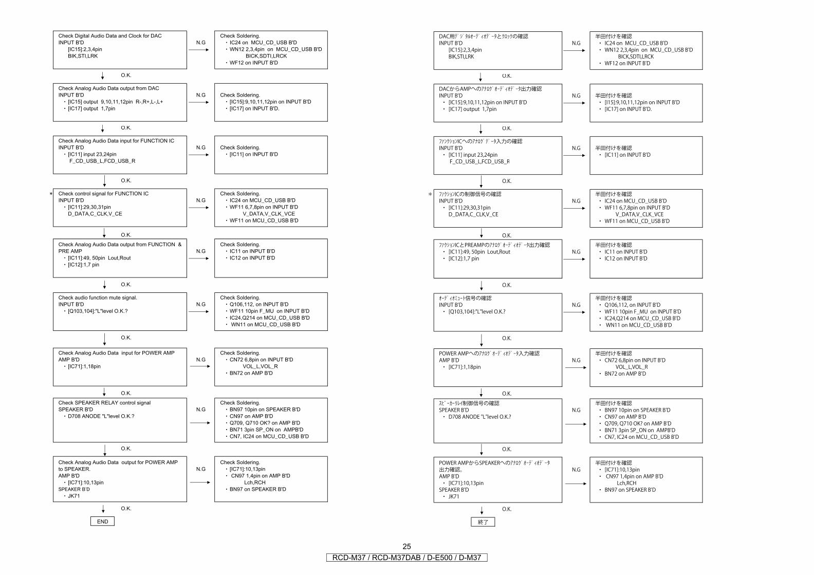
Check Digital Audio Data and Clock for DAC Check Soldering.INPUT B'D N.G IC24 on MCU_CD_USB B'D
[IC15]:2,3,4pin WN12 2,3,4pin on MCU_CD_USB B'DBIK,STI,LRK BICK,SDTI,LRCK
WF12 on INPUT B'D
O.K.
Check Analog Audio Data output from DACINPUT B'D N.G Check Soldering.
[IC15] output 9,10,11,12pin R-,R+,L-,L+ [IC15]:9,10,11,12pin on INPUT B'D[IC17] output 1,7pin [IC17] on INPUT B'D.
O.K.
Check Analog Audio Data input for FUNCTION ICINPUT B'D N.G Check Soldering.
[IC11] input 23,24pin [IC11] on INPUT B'D F_CD_USB_L,FCD_USB_R
O.K.
Check control signal for FUNCTION IC Check Soldering.INPUT B'D N.G IC24 on MCU_CD_USB B'D
[IC11]:29,30,31pin WF11 6,7,8pin on INPUT B'DD_DATA,C_CLK,V_CE V_DATA,V_CLK_VCE
WF11 on MCU_CD_USB B'D
O.K.
Check Analog Audio Data output from FUNCTION & Check Soldering.PRE AMP N.G IC11 on INPUT B'D
[IC11]:49, 50pin Lout,Rout IC12 on INPUT B'D[IC12]:1,7 pin
O.K.
Check audio function mute signal. Check Soldering.INPUT B'D N.G Q106,112, on INPUT B'D
[Q103,104]:"L"level O.K.? WF11 10pin F_MU on INPUT B'DIC24,Q214 on MCU_CD_USB B'D WN11 on MCU_CD_USB B'D
O.K.
Check Analog Audio Data input for POWER AMP Check Soldering.AMP B'D N.G CN72 6,8pin on INPUT B'D
[IC71]:1,18pin VOL_L,VOL_RBN72 on AMP B'D
O.K.
Check SPEAKER RELAY control signal Check Soldering.SPEAKER B'D N.G BN97 10pin on SPEAKER B'D
D708 ANODE "L"level O.K.? CN97 on AMP B'DQ709, Q710 OK? on AMP B'DBN71 3pin SP_ON on AMPB'DCN7, IC24 on MCU_CD_USB B'D
O.K.
Check Analog Audio Data output for POWER AMP Check Soldering.to SPEAKER. N.G [IC71]:10,13pinAMP B'D CN97 1,4pin on AMP B'D
[IC71]:10,13pin Lch,RCHBN97 on SPEAKER B'D
JK71
O.K.
END
2RCD-M37 / RCD-M37
DAC用デジタルオーディオデータとクロックの確認 半田付けを確認INPUT B'D N.G ・ IC24 on MCU_CD_USB B'D
[IC15]:2,3,4pin ・ WN12 2,3,4pin on MCU_CD_USB B'DBIK,STI,LRK BICK,SDTI,LRCK
・ WF12 on INPUT B'D
O.K.
DACからAMPへのアナログオーディオデータ出力確認INPUT B'D N.G 半田付けを確認・ [IC15]:9,10,11,12pin on INPUT B'D ・ [I15]:9,10,11,12pin on INPUT B'D・ [IC17] output 1,7pin ・ [IC17] on INPUT B'D.
O.K.
ファンクションICへのアナログデータ入力の確認INPUT B'D N.G 半田付けを確認・ [IC11] input 23,24pin ・ [IC11] on INPUT B'D
F_CD_USB_L,FCD_USB_R
O.K.
* ファクションICの制御信号の確認 半田付けを確認INPUT B'D N.G ・ IC24 on MCU_CD_USB B'D・ [IC11]:29,30,31pin ・ WF11 6,7,8pin on INPUT B'D
D_DATA,C_CLK,V_CE V_DATA,V_CLK_VCE・ WF11 on MCU_CD_USB B'D
O.K.
ファクションICとPREAMPのアナログオーディオデータ出力確認 半田付けを確認・ [IC11]:49, 50pin Lout,Rout N.G ・ IC11 on INPUT B'D・ [IC12]:1,7 pin ・ IC12 on INPUT B'D
O.K.
オーディオミュート信号の確認 半田付けを確認INPUT B'D N.G ・ Q106,112, on INPUT B'D・ [Q103,104]:"L"level O.K.? ・ WF11 10pin F_MU on INPUT B'D
・ IC24,Q214 on MCU_CD_USB B'D・ WN11 on MCU_CD_USB B'D
O.K.
POWER AMPへのアナログオーディオデータ入力確認 半田付けを確認AMP B'D N.G ・ CN72 6,8pin on INPUT B'D・ [IC71]:1,18pin VOL_L,VOL_R
・ BN72 on AMP B'D
O.K.
スピーカーリレイ制御信号の確認 半田付けを確認SPEAKER B'D N.G ・ BN97 10pin on SPEAKER B'D・ D708 ANODE "L"level O.K.? ・ CN97 on AMP B'D
・ Q709, Q710 OK? on AMP B'D・ BN71 3pin SP_ON on AMPB'D・ CN7, IC24 on MCU_CD_USB B'D
O.K.
POWER AMPからSPEAKERへのアナログオーディオデータ 半田付けを確認出力確認。 N.G ・ [IC71]:10,13pinAMP B'D ・ CN97 1,4pin on AMP B'D・ [IC71]:10,13pin Lch,RCH
SPEAKER B'D ・ BN97 on SPEAKER B'D・ JK71
O.K.
終了
5DAB / D-E500 / D-M37
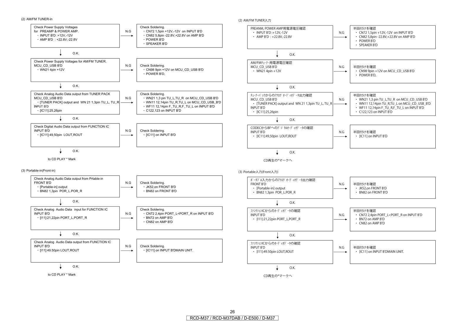
(2) AM/FM TUNER-in
Check Power Supply Voltages Check Soldering.for PREAMP & POWER AMP. N.G CN72 1,5pin +12V,-12V on INPUT B'D
INPUT B'D :+12V,-12V CN82 5,8pin -22.8V,+22.8V on AMP B'DAMP B'D : +22.8V,-22.8V POWER B'D
SPEAKER B'D
O.K.
Check Power Supply Voltages for AM/FM TUNER.MCU_CD_USB B'D N.G Check Soldering.
WN21 4pin +12V CN98 9pin +12V on MCU_CD_USB B'DPOWER B'D,
O.K.
Check Analog Audio Data output from TUNER PACK Check Soldering.MCU_CD_USB B'D N.G WN21 1,3 pin TU_L,TU_R on MCU_CD_USB B'D
[TUNER PACK] output and WN 21 1,3pin TU_L, TU_R WN11 12,14pin TU_R,TU_L on MCU_CD_USB_B'DWF11 12,14pin F_TU_R,F_TU_L on INPUT B'D
[IC11]:25,26pin C122,123 on INPUT B'D
O.K.
Check Digital Audio Data output from FUNCTION ICINPUT B'D N.G Check Soldering.
[IC11]:49,50pin LOUT,ROUT [IC11] on INPUT B'D
O.K.
to CD PLAY * Mark
(3) Portable-in(Front-in)
Check Analog Audio Data output from Prtable-inFRONT B'D N.G Check Soldering.
[Portable-in] output JK52,on FRONT B'DBN82 1,3pin POR_L.POR_R BN82 on FRONT B'D
O.K.
Check Analog Audio Data input for FUNCTION IC Check Soldering.INPUT B'D N.G CN72 2,4pin PORT_L<PORT_R on INPUT B'D
[I11]:21,22pin PORT_L,PORT_R BN72 on AMP B'DCN82 on AMP B'D
O.K.
Check Analog Audio Data output from FUNCTION ICINPUT B'D N.G Check Soldering.
[I11]:49.50pin LOUT,ROUT [IC11] on INPUT B'DMAIN UNIT.
O.K.
to CD PLAY * Mark
2RCD-M37 / RCD-M37
(2) AM/FM TUNER入力
PREANM, POWER AMP用電源電圧確認 半田付けを確認・ INPUT B'D :+12V,-12V N.G ・ CN72 1,5pin +12V,-12V on INPUT B'D・ AMP B'D : +22.8V,-22.8V ・ CN82 5,8pin -22.8V,+22.8V on AMP B'D
・ POWER B'D・ SPEAKER B'D
O.K.
AM/FMチューナー用電源電圧確認MCU_CD_USB B'D N.G 半田付けを確認・ WN21 4pin +12V ・ CN98 9pin +12V on MCU_CD_USB B'D
・ POWER B'D,
O.K.
チューナーパックからのアナログオーディオデータ出力確認 半田付けを確認MCU_CD_USB B'D N.G ・ WN21 1,3 pin TU_L,TU_R on MCU_CD_USB B'D・ [TUNER PACK] output and WN 21 1,3pin TU_L, TU_R ・ WN11 12,14pin TU_R,TU_L on MCU_CD_USB_B'D
INPUT B'D ・ WF11 12,14pin F_TU_R,F_TU_L on INPUT B'D・ [IC11]:25,26pin ・ C122,123 on INPUT B'D
O.K.
CODECからBFへのデジタルオーディオデータの確認INPUT B'D N.G 半田付けを確認・ [IC11]:49,50pin LOUT,ROUT ・ [IC11] on INPUT B'D
O.K.
CD再生の*マークへ
(3) Portable入力(Front入力)
ポータブル入力からのアナログオーディオデータ出力確認FRONT B'D N.G 半田付けを確認・ [Portable-in] output ・ JK52,on FRONT B'D・ BN82 1,3pin POR_L.POR_R ・ BN82 on FRONT B'D
O.K.
ファンクションICからのオーディオデータの確認 半田付けを確認INPUT B'D N.G ・ CN72 2,4pin PORT_L<PORT_R on INPUT B'D・ [I11]:21,22pin PORT_L,PORT_R ・ BN72 on AMP B'D
・ CN82 on AMP B'D
O.K.
ファンクションICからのオーディオデータの確認INPUT B'D N.G 半田付けを確認・ [I11]:49.50pin LOUT,ROUT ・ [IC11] on INPUT B'DMAIN UNIT.
O.K.
CD再生の*マークへ
6DAB / D-E500 / D-M37
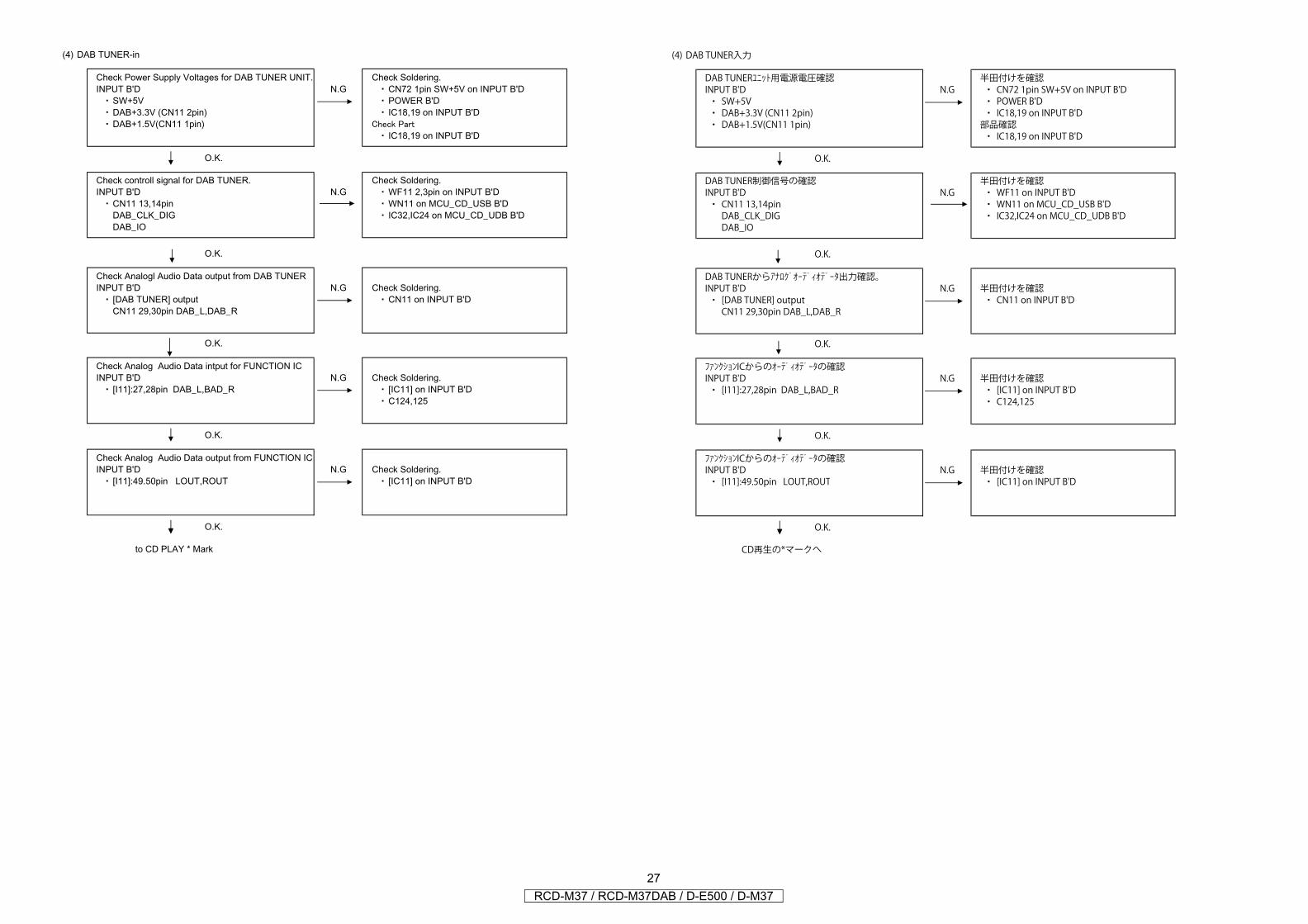
(4) DAB TUNER-in
Check Power Supply Voltages for DAB TUNER UNIT. Check Soldering.INPUT B'D N.G CN72 1pin SW+5V on INPUT B'D
SW+5V POWER B'DDAB+3.3V (CN11 2pin) IC18,19 on INPUT B'DDAB+1.5V(CN11 1pin)
IC18,19 on INPUT B'D
O.K.
Check controll signal for DAB TUNER. Check Soldering.INPUT B'D N.G WF11 2,3pin on INPUT B'D
CN11 13,14pin WN11 on MCU_CD_USB B'DDAB_CLK_DIG IC32,IC24 on MCU_CD_UDB B'DDAB_IO
O.K.
Check Analogl Audio Data output from DAB TUNERINPUT B'D N.G Check Soldering.
[DAB TUNER] output CN11 on INPUT B'DCN11 29,30pin DAB_L,DAB_R
O.K.
Check Analog Audio Data intput for FUNCTION ICINPUT B'D N.G Check Soldering.
[I11]:27,28pin DAB_L,BAD_R [IC11] on INPUT B'DC124,125
O.K.
Check Analog Audio Data output from FUNCTION ICINPUT B'D N.G Check Soldering.
[I11]:49.50pin LOUT,ROUT [IC11] on INPUT B'D
O.K.
to CD PLAY * Mark
2RCD-M37 / RCD-M37
(4) DAB TUNER入力
DAB TUNERユニット用電源電圧確認 半田付けを確認INPUT B'D N.G ・ CN72 1pin SW+5V on INPUT B'D・ SW+5V ・ POWER B'D・ DAB+3.3V (CN11 2pin) ・ IC18,19 on INPUT B'D・ DAB+1.5V(CN11 1pin) 部品確認
・ IC18,19 on INPUT B'D
O.K.
DAB TUNER制御信号の確認 半田付けを確認INPUT B'D N.G ・ WF11 on INPUT B'D・ CN11 13,14pin ・ WN11 on MCU_CD_USB B'D
DAB_CLK_DIG ・ IC32,IC24 on MCU_CD_UDB B'DDAB_IO
O.K.
DAB TUNERからアナログオーディオデータ出力確認。INPUT B'D N.G 半田付けを確認・ [DAB TUNER] output ・ CN11 on INPUT B'D
CN11 29,30pin DAB_L,DAB_R
O.K.
ファンクションICからのオーディオデータの確認INPUT B'D N.G 半田付けを確認・ [I11]:27,28pin DAB_L,BAD_R ・ [IC11] on INPUT B'D
・ C124,125
O.K.
ファンクションICからのオーディオデータの確認INPUT B'D N.G 半田付けを確認・ [I11]:49.50pin LOUT,ROUT ・ [IC11] on INPUT B'D
O.K.
CD再生の*マークへ
7DAB / D-E500 / D-M37
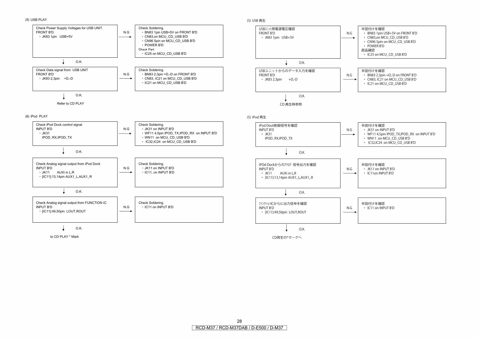
(5) USB PLAY
Check Power Supply Voltages for USB UNIT. Check Soldering.FRONT B'D N.G BN83 1pin USB+5V on FRONT B'D
JK83 1pin USB+5V CN83,on MCU_CD_USB B'DCN96 5pin on MCU_CD_USB B'DPOWER B'D
IC25 on MCU_CD_USB B'D
O.K.
Check Data signal from USB UNIT Check Soldering.FRONT B'D N.G BN83 2,3pin +D,-D on FRONT B'D
JK83 2,3pin +D,-D CN83, IC21 on MCU_CD_USB B'DIC21 on MCU_CD_USB B'D
O.K.
Refer to CD PLAY
(6) iPod PLAY
Check iPod Dock control signal Check Soldering.INPUT B'D N.G JK31 on INPUT B'D
JK31 WF11 4,5pin IPOD_TX,IPOD_RX on INPUT B'DIPOD_RX,IPOD_TX WN11 on MCU_CD_USB B'D
IC32,IC24 on MCU_CD_USB B'D
O.K.
Check Analog signal output from iPod Dock Check Soldering.INPUT B'D N.G JK11 on INPUT B'D
JK11 AUXi in L,R IC11, on INPUT B'D[IC11]:13,14pin AUX1_L,AUX1_R
O.K.
Check Analog signal output from FUNCTION IC Check Soldering.INPUT B'D N.G IC11 on INPUT B'D
[IC11]:49,50pin LOUT,ROUT
O.K.
to CD PLAY * Mark
2RCD-M37 / RCD-M37
(5) USB 再生
USBユニット用電源電圧確認 半田付けを確認FRONT B'D N.G ・ BN83 1pin USB+5V on FRONT B'D・ JK83 1pin USB+5V ・ CN83,on MCU_CD_USB B'D
・ CN96 5pin on MCU_CD_USB B'D・ POWER B'D
部品確認・ IC25 on MCU_CD_USB B'D
O.K.
USBユニットからのデータ入力を確認 半田付けを確認FRONT B'D N.G ・ BN83 2,3pin +D,-D on FRONT B'D・ JK83 2,3pin +D,-D ・ CN83, IC21 on MCU_CD_USB B'D
・ IC21 on MCU_CD_USB B'D
O.K.
CD 再生時参照
(5) iPod 再生
iPod Dock制御信号を確認 半田付けを確認INPUT B'D N.G ・ JK31 on INPUT B'D・ JK31 ・ WF11 4,5pin IPOD_TX,IPOD_RX on INPUT B'D
IPOD_RX,IPOD_TX ・ WN11 on MCU_CD_USB B'D・ IC32,IC24 on MCU_CD_USB B'D
O.K.
iPOd Dockからのアナログ信号出力を確認 半田付けを確認INPUT B'D N.G ・ JK11 on INPUT B'D・ JK11 AUXi in L,R ・ IC11on INPUT B'D・ [IC11]:13,14pin AUX1_L,AUX1_R
O.K.
ファンクションICからに出力信号を確認 半田付けを確認INPUT B'D N.G ・ IC11 on INPUT B'D・ [IC11]:49,50pin LOUT,ROUT
O.K.
CD再生の*マークへ
8DAB / D-E500 / D-M37
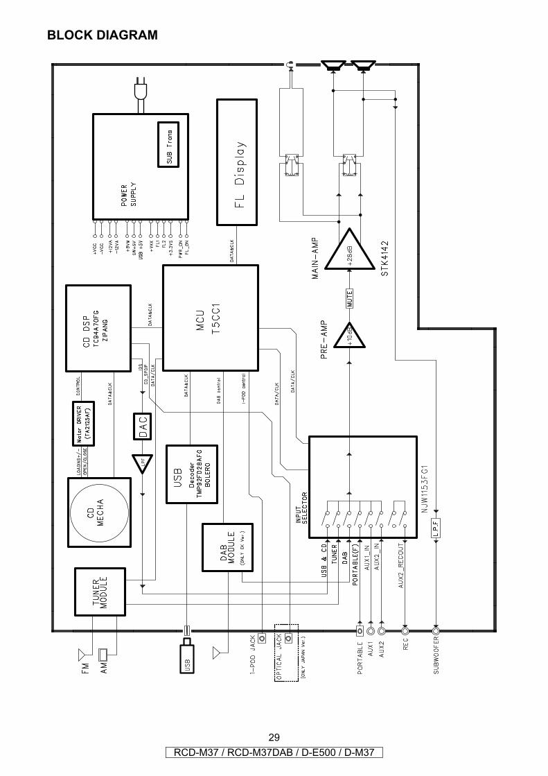
BLOCK DIAGRAM
29RCD-M37 / RCD-M37DAB / D-E500 / D-M37
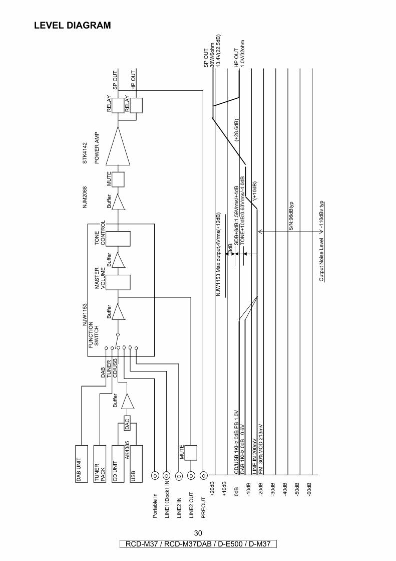
LEVEL DIAGRAM
DABUNIT
NJW1153
NJM2068
STK4142
FUNCTION
TUNER
SWITCH
MASTER
TONE
POWERAMP
PACK
DAB
VOLUME
CONTROL
TUNER
Buffer
Buffer
Buffer
MUTE
RELAY
CDUNIT
Buffer
CD/USB
SPOUT
AK4385
DAC
RELAY
USB
HPOUT
PortableIn
LINE1DockIN
LINE2IN
MUTE
LINE2OUT
PREOUT
SPOUT
+20dB
30W/6ohm
NJW1153Maxoutput,4Vrms(+12dB)
13.4V(22.5dB)
+10dB
8dB
0dB
CD/USB1KHz0dBPB1.0V
SDB+8dB:1.59Vrms/+4dB
(+28.6dB)
HPOUT
DAB1KHz0dB
0.6V
TONE+10dB:0.63Vrms/-4.0dB
1.0V/32ohm
-10dB
LINEIN200mV
'(+10dB)
-20dB
FM30%MOD213mV
-30dB
-40dB
S/N:96dBtyp
-50dB
-60dB
OutputNoiseLevel
-110dBvtyp
30RCD-M37 / RCD-M37DAB / D-E500 / D-M37
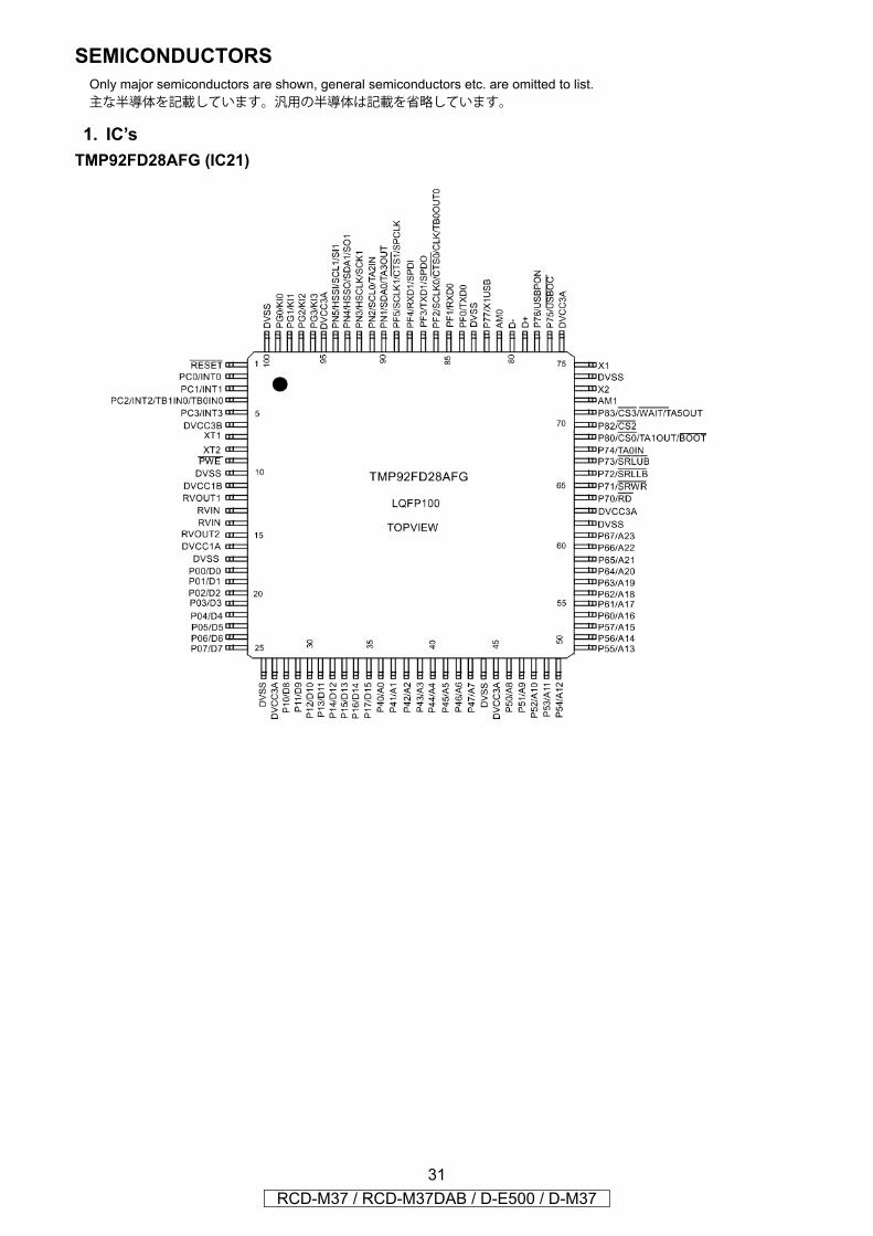
SEMICONDUCTORSOnly major semiconductors are shown, general semiconductors etc. are omitted to list.主な半導体を記載しています。汎用の半導体は記載を省略しています。
1. IC’sTMP92FD28AFG (IC21)
31RCD-M37 / RCD-M37DAB / D-E500 / D-M37

TMP92FD28AFG Block diagram
32RCD-M37 / RCD-M37DAB / D-E500 / D-M37
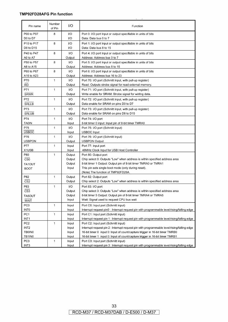
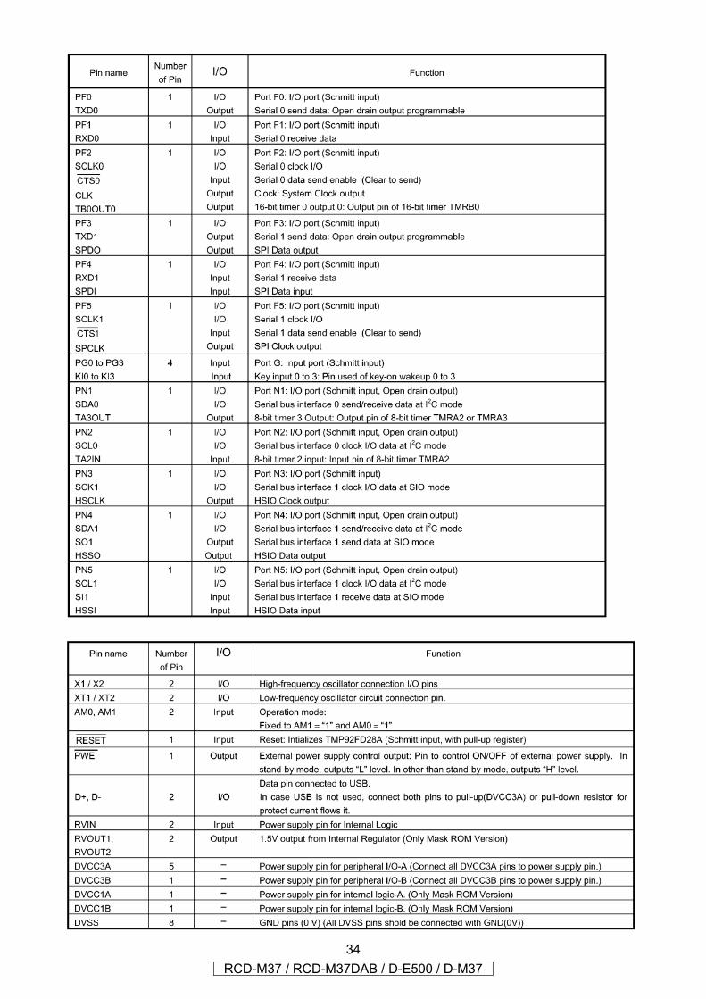
TMP92FD28AFG Pin function
33RCD-M37 / RCD-M37DAB / D-E500 / D-M37
34RCD-M37 / RCD-M37DAB / D-E500 / D-M37
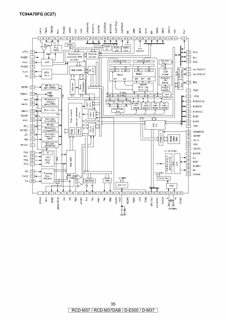
TC94A70FG (IC27)
35RCD-M37 / RCD-M37DAB / D-E500 / D-M37
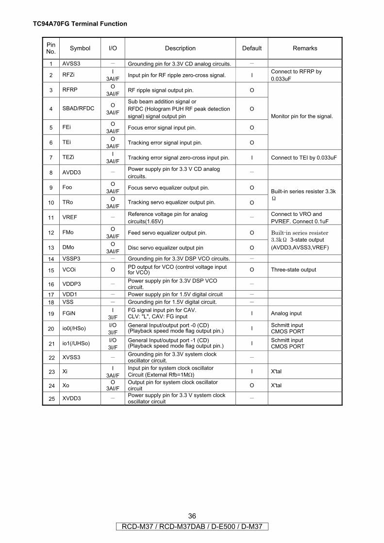
TC94A70FG Terminal Function
Pin
No.Symbol I/O Description Default Remarks
1 AVSS3 Grounding pin for 3.3V CD analog circuits.
2 RFZiI
3AI/FInput pin for RF ripple zero-cross signal. I
Connect to RFRP by
0.033uF
3 RFRPO
3AI/FRF ripple signal output pin. O
4 SBAD/RFDCO
3AI/F
Sub beam addition signal or
RFDC (Hologram PUH RF peak detection
signal) signal output pin
O
5 FEiO
3AI/FFocus error signal input pin. O
6 TEi O
3AI/FTracking error signal input pin. O
Monitor pin for the signal.
7 TEZi I
3AI/FTracking error signal zero-cross input pin. I Connect to TEI by 0.033uF
8 AVDD3Power supply pin for 3.3 V CD analog
circuits.
9 Foo O
3AI/FFocus servo equalizer output pin. O
10 TRo O
3AI/FTracking servo equalizer output pin. O
Built-in series resister 3.3k
11 VREFReference voltage pin for analog
circuits(1.65V)
Connect to VRO and
PVREF. Connect 0.1uF
12 FMo O
3AI/FFeed servo equalizer output pin. O
13 DMoO
3AI/FDisc servo equalizer output pin O
Built-in series resister
3.3k 3-state output
(AVDD3,AVSS3,VREF)
14 VSSP3 Grounding pin for 3.3V DSP VCO circuits.
15 VCOi O PD output for VCO (control voltage input
for VCO) O Three-state output
16 VDDP3Power supply pin for 3.3V DSP VCO
circuit.
17 VDD1 Power supply pin for 1.5V digital circuit
18 VSS Grounding pin for 1.5V digital circuit.
19 FGiNI
3I/F
FG signal input pin for CAV.
CLV: "L", CAV: FG input I Analog input
20 io0(/HSo)I/O
3I/F
General Input/output port -0 (CD)
(Playback speed mode flag output pin.) I
Schmitt input
CMOS PORT
21 io1(/UHSo) I/O
3I/F
General Input/output port -1 (CD)
(Playback speed mode flag output pin.) I
Schmitt input
CMOS PORT
22 XVSS3 Grounding pin for 3.3V system clock
oscillator circuit.
23 XiI
3AI/F
Input pin for system clock oscillator
Circuit (External Rfb=1M )I X'tal
24 XoO
3AI/F
Output pin for system clock oscillator
circuitO X'tal
25 XVDD3 Power supply pin for 3.3 V system clock
oscillator circuit
36RCD-M37 / RCD-M37DAB / D-E500 / D-M37
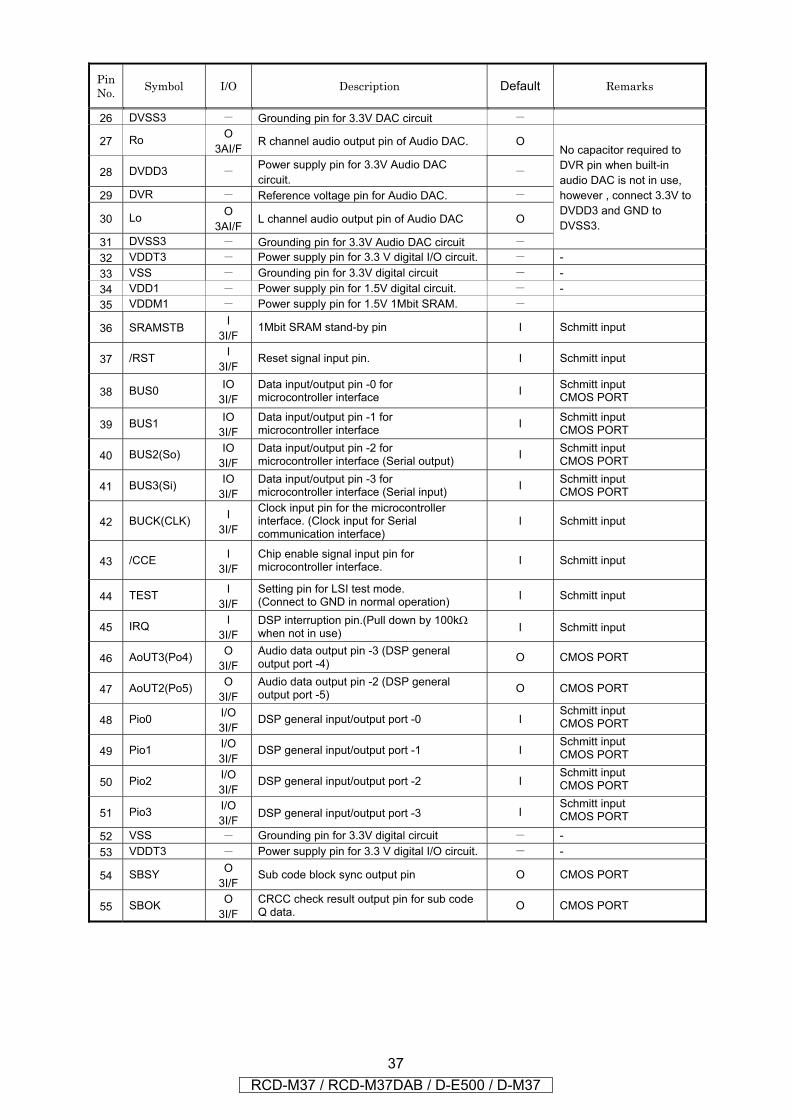
Pin
No.Symbol I/O Description Default Remarks
26 DVSS3 Grounding pin for 3.3V DAC circuit
27 RoO
3AI/FR channel audio output pin of Audio DAC. O
28 DVDD3Power supply pin for 3.3V Audio DAC
circuit.
29 DVR Reference voltage pin for Audio DAC.
30 LoO
3AI/FL channel audio output pin of Audio DAC O
31 DVSS3 Grounding pin for 3.3V Audio DAC circuit
No capacitor required to
DVR pin when built-in
audio DAC is not in use,
however , connect 3.3V to
DVDD3 and GND to
DVSS3.
32 VDDT3 Power supply pin for 3.3 V digital I/O circuit. -
33 VSS Grounding pin for 3.3V digital circuit -
34 VDD1 Power supply pin for 1.5V digital circuit. -
35 VDDM1 Power supply pin for 1.5V 1Mbit SRAM.
36 SRAMSTB I
3I/F1Mbit SRAM stand-by pin I Schmitt input
37 /RST I
3I/FReset signal input pin. I Schmitt input
38 BUS0IO
3I/F
Data input/output pin -0 for
microcontroller interface I
Schmitt input
CMOS PORT
39 BUS1IO
3I/F
Data input/output pin -1 for
microcontroller interface I
Schmitt input
CMOS PORT
40 BUS2(So)IO
3I/F
Data input/output pin -2 for
microcontroller interface (Serial output) I
Schmitt input
CMOS PORT
41 BUS3(Si)IO
3I/F
Data input/output pin -3 for
microcontroller interface (Serial input) I
Schmitt input
CMOS PORT
42 BUCK(CLK)I
3I/F
Clock input pin for the microcontroller
interface. (Clock input for Serial
communication interface)
I Schmitt input
43 /CCEI
3I/F
Chip enable signal input pin for
microcontroller interface. I Schmitt input
44 TEST I
3I/F
Setting pin for LSI test mode.
(Connect to GND in normal operation) I Schmitt input
45 IRQI
3I/F
DSP interruption pin.(Pull down by 100k
when not in use) I Schmitt input
46 AoUT3(Po4) O
3I/F
Audio data output pin -3 (DSP general
output port -4) O CMOS PORT
47 AoUT2(Po5) O
3I/F
Audio data output pin -2 (DSP general
output port -5) O CMOS PORT
48 Pio0I/O
3I/FDSP general input/output port -0 I
Schmitt input
CMOS PORT
49 Pio1I/O
3I/FDSP general input/output port -1 I
Schmitt input
CMOS PORT
50 Pio2I/O
3I/FDSP general input/output port -2 I
Schmitt input
CMOS PORT
51 Pio3I/O
3I/FDSP general input/output port -3 I
Schmitt input
CMOS PORT
52 VSS Grounding pin for 3.3V digital circuit -
53 VDDT3 Power supply pin for 3.3 V digital I/O circuit. -
54 SBSYO
3I/FSub code block sync output pin O CMOS PORT
55 SBOKO
3I/F
CRCC check result output pin for sub code
Q data. O CMOS PORT
37RCD-M37 / RCD-M37DAB / D-E500 / D-M37
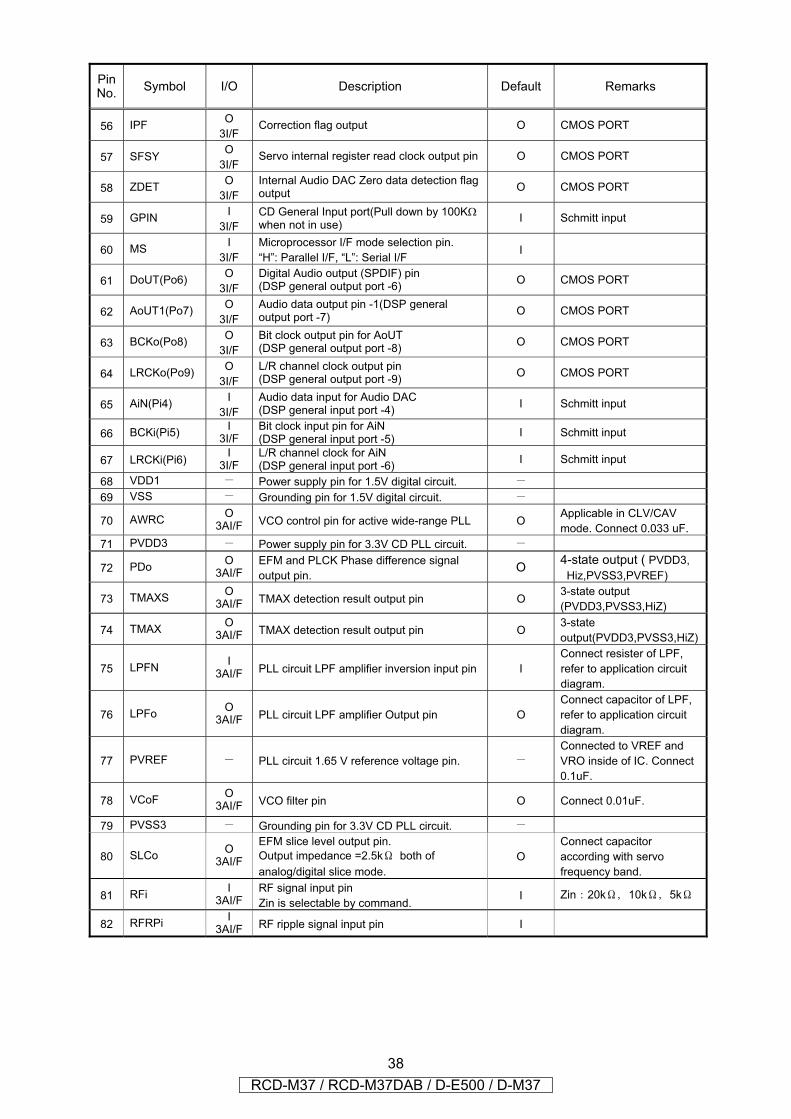
Pin
No.Symbol I/O Description Default Remarks
56 IPFO
3I/FCorrection flag output O CMOS PORT
57 SFSYO
3I/FServo internal register read clock output pin O CMOS PORT
58 ZDET O
3I/F
Internal Audio DAC Zero data detection flag
outputO CMOS PORT
59 GPINI
3I/F
CD General Input port(Pull down by 100K
when not in use) I Schmitt input
60 MSI
3I/F
Microprocessor I/F mode selection pin.
“H”: Parallel I/F, “L”: Serial I/F I
61 DoUT(Po6) O
3I/F
Digital Audio output (SPDIF) pin
(DSP general output port -6) O CMOS PORT
62 AoUT1(Po7) O
3I/F
Audio data output pin -1(DSP general
output port -7) O CMOS PORT
63 BCKo(Po8)O
3I/F
Bit clock output pin for AoUT
(DSP general output port -8) O CMOS PORT
64 LRCKo(Po9) O
3I/F
L/R channel clock output pin
(DSP general output port -9) O CMOS PORT
65 AiN(Pi4)I
3I/F
Audio data input for Audio DAC
(DSP general input port -4) I Schmitt input
66 BCKi(Pi5)I
3I/F
Bit clock input pin for AiN
(DSP general input port -5) I Schmitt input
67 LRCKi(Pi6) I
3I/F
L/R channel clock for AiN
(DSP general input port -6) I Schmitt input
68 VDD1 Power supply pin for 1.5V digital circuit.
69 VSS Grounding pin for 1.5V digital circuit.
70 AWRCO
3AI/FVCO control pin for active wide-range PLL O
Applicable in CLV/CAV
mode. Connect 0.033 uF.
71 PVDD3 Power supply pin for 3.3V CD PLL circuit.
72 PDoO
3AI/F
EFM and PLCK Phase difference signal
output pin. O
4-state output ( PVDD3,
Hiz,PVSS3,PVREF)
73 TMAXS O
3AI/FTMAX detection result output pin O
3-state output
(PVDD3,PVSS3,HiZ)
74 TMAX O
3AI/FTMAX detection result output pin O
3-state
output(PVDD3,PVSS3,HiZ)
75 LPFN I
3AI/FPLL circuit LPF amplifier inversion input pin I
Connect resister of LPF,
refer to application circuit
diagram.
76 LPFo O
3AI/FPLL circuit LPF amplifier Output pin O
Connect capacitor of LPF,
refer to application circuit
diagram.
77 PVREF PLL circuit 1.65 V reference voltage pin.
Connected to VREF and
VRO inside of IC. Connect
0.1uF.
78 VCoFO
3AI/FVCO filter pin O Connect 0.01uF.
79 PVSS3 Grounding pin for 3.3V CD PLL circuit.
80 SLCoO
3AI/F
EFM slice level output pin.
Output impedance =2.5k both of
analog/digital slice mode.
O
Connect capacitor
according with servo
frequency band.
81 RFiI
3AI/F
RF signal input pin
Zin is selectable by command. I Zin 20k 10k 5k
82 RFRPiI
3AI/FRF ripple signal input pin I
38RCD-M37 / RCD-M37DAB / D-E500 / D-M37
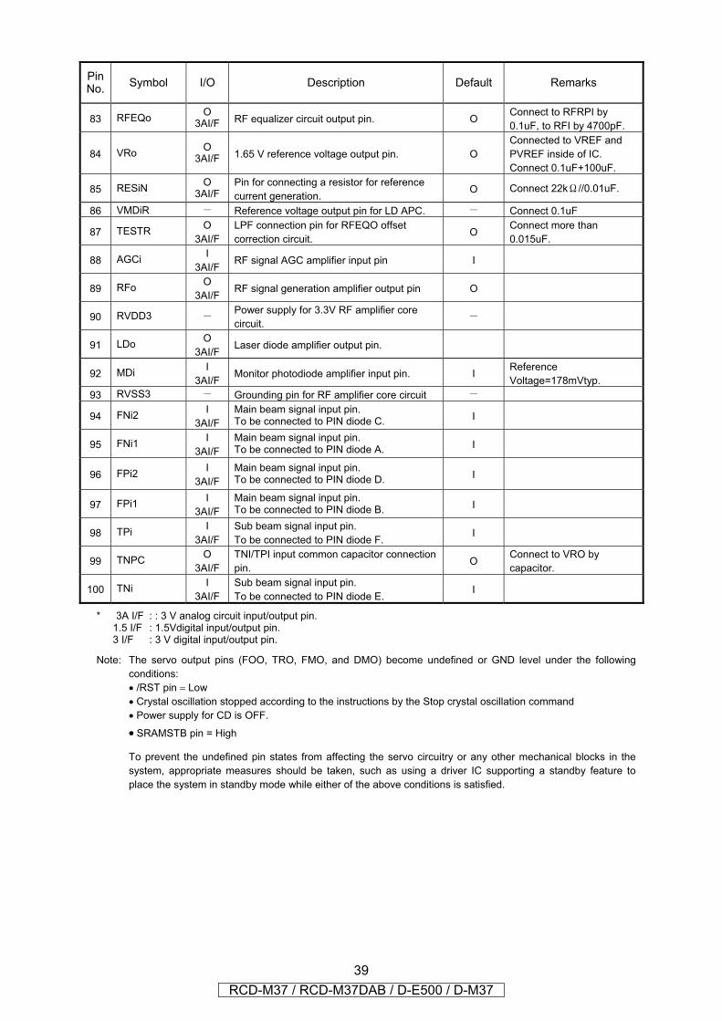
Pin
No.Symbol I/O Description Default Remarks
83 RFEQoO
3AI/FRF equalizer circuit output pin. O
Connect to RFRPI by
0.1uF, to RFI by 4700pF.
84 VRoO
3AI/F1.65 V reference voltage output pin. O
Connected to VREF and
PVREF inside of IC.
Connect 0.1uF+100uF.
85 RESiNO
3AI/F
Pin for connecting a resistor for reference
current generation. O Connect 22k //0.01uF.
86 VMDiR Reference voltage output pin for LD APC. Connect 0.1uF
87 TESTR O
3AI/F
LPF connection pin for RFEQO offset
correction circuit. O
Connect more than
0.015uF.
88 AGCiI
3AI/FRF signal AGC amplifier input pin I
89 RFoO
3AI/FRF signal generation amplifier output pin O
90 RVDD3Power supply for 3.3V RF amplifier core
circuit.
91 LDoO
3AI/FLaser diode amplifier output pin.
92 MDiI
3AI/FMonitor photodiode amplifier input pin. I
Reference
Voltage=178mVtyp.
93 RVSS3 Grounding pin for RF amplifier core circuit
94 FNi2I
3AI/F
Main beam signal input pin.
To be connected to PIN diode C. I
95 FNi1I
3AI/F
Main beam signal input pin.
To be connected to PIN diode A. I
96 FPi2 I
3AI/F
Main beam signal input pin.
To be connected to PIN diode D. I
97 FPi1 I
3AI/F
Main beam signal input pin.
To be connected to PIN diode B. I
98 TPi I
3AI/F
Sub beam signal input pin.
To be connected to PIN diode F. I
99 TNPC O
3AI/F
TNI/TPI input common capacitor connection
pin.O
Connect to VRO by
capacitor.
100 TNi I
3AI/F
Sub beam signal input pin.
To be connected to PIN diode E. I
* 3A I/F : : 3 V analog circuit input/output pin.
1.5 I/F : 1.5Vdigital input/output pin.
3 I/F : 3 V digital input/output pin.
Note: The servo output pins (FOO, TRO, FMO, and DMO) become undefined or GND level under the following
conditions:
/RST pin Low
Crystal oscillation stopped according to the instructions by the Stop crystal oscillation command
Power supply for CD is OFF.
SRAMSTB pin = High
To prevent the undefined pin states from affecting the servo circuitry or any other mechanical blocks in the
system, appropriate measures should be taken, such as using a driver IC supporting a standby feature to
place the system in standby mode while either of the above conditions is satisfied.
39RCD-M37 / RCD-M37DAB / D-E500 / D-M37
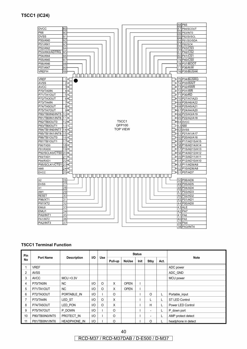
T5CC1 (IC24)
T5CC1 Terminal Function
PinNo Port Name Description I/O Use
StatusNote
Pull-up NoUse Init Stby Act.
1 VREF ADC power2 AVSS ADC_GND3 AVCC MCU +3.3V MCU power4 P70/TA0IN NC I/O O X OPEN I5 P71/TA1OUT NC I/O O X OPEN I6 P72/TA3OUT PORTABLE_IN I/O I O I O L Portable_input7 P73/TA4IN LED_ST I/O O X I L L ST LED Control8 P74/TA5OUT LED_PON I/O O X I H L Power LED Control9 P75/TA7OUT P_DOWN I/O I O I - L P_down port10 P80/TB0IN0/INT5 PROTECT_IN I/O I O I - L AMP protect detect11 P81/TB0IN1/INT6 HEADPHONE_IN I/O I O I O L headphone in detect
P65DVCC P64/SCOUT
P66 P63/INT0
DVSS P62/SI/SCL
P50/AN0 P61/SO/SDA
P51/AN1 P60/SCK
P52/AN2 P43/CS3P53/AN3/ADTRG P42/CS2P54/AN4 P41/CS1P55/AN5 P40/CS0P56/AN6 P37/BOOTP57/AN7 P36/R/WVREFH P35/BUSAK
VREF P34/BUSRQAVSS P33/WAITAVCC P32/HWRP70/TA0IN P31/WRP71/TA1OUT P30/RDP72/TA3OUT P27/A7/A23P73/TA4IN P26/A6/A22P74/TA5OUT P25/A5/A21P75/TA7OUT P24/A4/A20P80/TB0IN0/INT5 P23/A3/A19P81/TB0IN1/INT6 P22/A2/A18P82/TB0OUT0 DVCC
P83/TB0OUT1 NMI
P84/TB1IN0/INT7 DVSS
P85/TB1IN1/INT8 P21/A1/A17P86/TB1OUT0 P20/A0/A16P87/TB1OUT1 P17/AD15/A15P90/TXD0 P16/AD14/A14P91/RXD0 P15/AD13/A13P92/SCLK0/CTS0 P14/AD12/A12P93/TXD1 P13/AD11/A11P94/RXD1 P12/AD10/A10P95/SCLK1/CTS1 P11/AD9/A9AM0 P10/AD8/A8DVCC P07/AD7
X2 P06/AD6DVSS P05/AD5X1 P04/AD4AM1 P03/AD3RESET P02/AD2P96/XT1 P01/AD1P97/XT2 P00/AD0EMU0 ALEEMU1 PA7PA0/INT1 PA6
PA1/INT2 PA5
PA2/INT3 PA4PA3/INT4
T5CC1QFP100
TOP VIEW
40RCD-M37 / RCD-M37DAB / D-E500 / D-M37
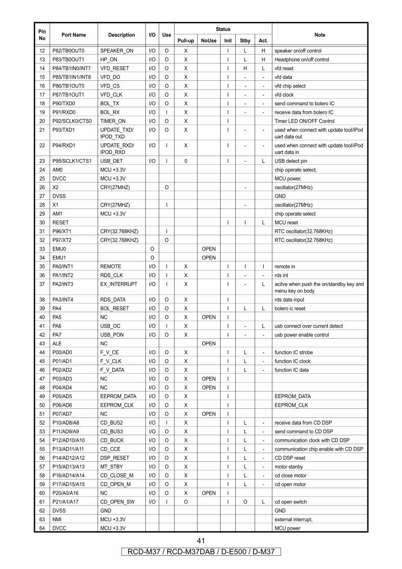
12 P82/TB0OUT0 SPEAKER_ON I/O O X I L H speaker on/off control13 P83/TB0OUT1 HP_ON I/O O X I L H Headphone on/off control14 P84/TB1IN0/INT7 VFD_RESET I/O O X I H L vfd reset15 P85/TB1IN1/INT8 VFD_DO I/O O X I - - vfd data16 P86/TB1OUT0 VFD_CS I/O O X I - - vfd chip select17 P87/TB1OUT1 VFD_CLK I/O O X I - - vfd clock18 P90/TXD0 BOL_TX I/O O X I - - send command to bolero IC19 P91/RXD0 BOL_RX I/O I X I - - receive data from bolero IC20 P92/SCLK0/CTS0 TIMER_ON I/O O X I Timer LED ON/OFF Control21 P93/TXD1 UPDATE_TXD/
IPOD_TXDI/O O X I - - used when connect with update tool/iPod
uart data out22 P94/RXD1 UPDATE_RXD/
IPOD_RXDI/O I X I - - used when connect with update tool/iPod
uart data in23 P95/SCLK1/CTS1 USB_DET I/O I 0 I - L USB detect pin24 AM0 MCU +3.3V chip operate select,25 DVCC MCU +3.3V MCU power,26 X2 CRY(27MHZ) O - oscillator(27MHz)27 DVSS GND28 X1 CRY(27MHZ) I - oscillator(27MHz)29 AM1 MCU +3.3V chip operate select30 RESET I I L MCU reset31 P96/XT1 CRY(32.768KHZ) I RTC oscillator(32.768KHz)32 P97/XT2 CRY(32.768KHZ) O RTC oscillator(32.768KHz)33 EMU0 O OPEN34 EMU1 O OPEN35 PA0/INT1 REMOTE I/O I X I I I remote in36 PA1/INT2 RDS_CLK I/O I X I - - rds int37 PA2/INT3 EX_INTERRUPT I/O I X I - L acitve when push the on/standby key and
menu key on body38 PA3/INT4 RDS_DATA I/O O X I rds data input39 PA4 BOL_RESET I/O O X I L L bolero ic reset40 PA5 NC I/O O X OPEN I41 PA6 USB_OC I/O I X I - L usb connect over current detect42 PA7 USB_PON I/O O X I - - usb power enable control43 ALE NC OPEN44 P00/AD0 F_V_CE I/O O X I L - function IC strobe45 P01/AD1 F_V_CLK I/O O X I L - function IC clock46 P02/AD2 F_V_DATA I/O O X I L - function IC data47 P03/AD3 NC I/O O X OPEN I48 P04/AD4 NC I/O O X OPEN I49 P05/AD5 EEPROM_DATA I/O O X I EEPROM_DATA50 P06/AD6 EEPROM_CLK I/O O X I EEPROM_CLK51 P07/AD7 NC I/O O X OPEN I52 P10/AD8/A8 CD_BUS2 I/O I X I L - receive data from CD DSP53 P11/AD9/A9 CD_BUS3 I/O O X I L - send command to CD DSP54 P12/AD10/A10 CD_BUCK I/O O X I L - communication clock with CD DSP55 P13/AD11/A11 CD_CCE I/O O X I L - communication chip enable with CD DSP56 P14/AD12/A12 DSP_RESET I/O O X I L - CD DSP reset57 P15/AD13/A13 MT_STBY I/O O X I L - motor stanby58 P16/AD14/A14 CD_CLOSE_M I/O O X I L - cd close motor59 P17/AD15/A15 CD_OPEN_M I/O O X I L - cd open motor60 P20/A0/A16 NC I/O O X OPEN I61 P21/A1/A17 CD_OPEN_SW I/O I O I O L cd open switch62 DVSS GND GND63 NMI MCU +3.3V external interrupt,64 DVCC MCU +3.3V MCU power
PinNo Port Name Description I/O Use
StatusNote
Pull-up NoUse Init Stby Act.
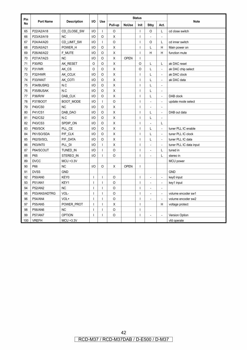
41RCD-M37 / RCD-M37DAB / D-E500 / D-M37
65 P22/A2/A18 CD_CLOSE_SW I/O I O I O L cd close switch66 P23/A3/A19 NC I/O O X I - -67 P24/A4/A20 CD_LIMIT_SW I/O I O I O L cd inner switch68 P25/A5/A21 POWER_H I/O O X I L H Main power on69 P26/A6/A22 F_MUTE I/O O X I H H function mute70 P27/A7/A23 NC I/O O X OPEN I71 P30/RD AK_RESET O O X O L L ak DAC reset72 P31/WR AK_CS O O X O L - ak DAC chip select73 P32/HWR AK_CCLK I/O O X I L - ak DAC clock74 P33/WAIT AK_COTI I/O O X I L - ak DAC data75 P34/BUSRQ N.C I/O O X I L -76 P35/BUSAK N.C I/O O X I L -77 P36/R/W DAB_CLK I/O O X I L - DAB clock78 P37/BOOT BOOT_MODE I/O I O I - - update mode select79 P40/CS0 NC I/O O X I - -80 P41/CS1 DAB_DAO I/O O X I L - DAB out data81 P42/CS2 N.C I/O O X I L -82 P43/CS3 SPDIP_ON I/O O X I - L83 P60/SCK PLL_CE I/O O X I L - tuner PLL IC enable84 P61/SO/SDA P/F_CLK I/O O X I L - tuner PLL IC clock85 P62/SI/SCL P/F_DATA I/O O X I L - tuner PLL IC data86 P63/INT0 PLL_DI I/O I X I - - tuner PLL IC data input87 P64/SCOUT TUNED_IN I/O I O I - L tuned in88 P65 STEREO_IN I/O I O I - L stereo in89 DVCC MCU +3.3V MCU power90 P66 NC I/O O X OPEN I91 DVSS GND GND92 P50/AN0 KEY0 I I O I - - key0 input93 P51/AN1 KEY1 I I O I - - key1 input94 P52/AN2 NC I I O I - - 95 P53/AN3/ADTRG VOL- I I O I - - volume encoder sw196 P54/AN4 VOL+ I I O I - - volume encoder sw297 P55/AN5 POWER_PROT I I X I H voltage protect98 P56/AN6 NC I I O I99 P57/AN7 OPTION I I O I - - Version Option100 VREFH MCU +3.3V vfd operate
PinNo Port Name Description I/O Use
StatusNote
Pull-up NoUse Init Stby Act.
42RCD-M37 / RCD-M37DAB / D-E500 / D-M37
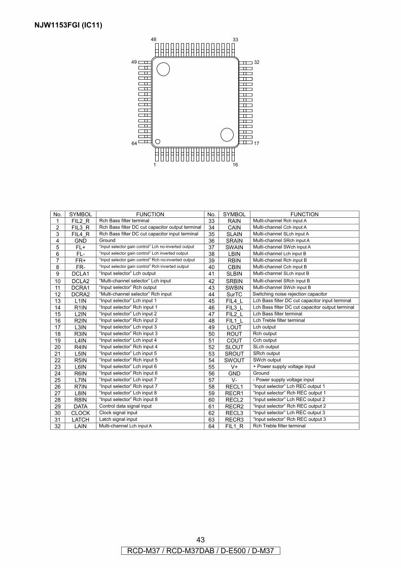
NJW1153FGI (IC11)
No. SYMBOL FUNCTION No. SYMBOL FUNCTION
1 FIL2_R Rch Bass filter terminal 33 RAIN Multi-channel Rch input A
2 FIL3_R Rch Bass filter DC cut capacitor output terminal 34 CAIN Multi-channel Cch input A
3 FIL4_R Rch Bass filter DC cut capacitor input terminal 35 SLAIN Multi-channel SLch input A
4 GND Ground 36 SRAIN Multi-channel SRch input A
5 FL+ “Input selector gain control” Lch no-inverted output 37 SWAIN Multi-channel SWch input A
6 FL- “Input selector gain control” Lch inverted output 38 LBIN Multi-channel Lch input B
7 FR+ “Input selector gain control” Rch no-inverted output 39 RBIN Multi-channel Rch input B
8 FR- “Input selector gain control” Rch inverted output 40 CBIN Multi-channel Cch input B
9 DCLA1 “Input selector” Lch output 41 SLBIN Multi-channel SLch input B
10 DCLA2 “Multi-channel selector” Lch input 42 SRBIN Multi-channel SRch input B
11 DCRA1 “Input selector” Rch output 43 SWBIN Multi-channel SWch input B
12 DCRA2 “Multi-channel selector” Rch input 44 SurTC Switching noise rejection capacitor
13 L1IN “Input selector” Lch input 1 45 FIL4_L Lch Bass filter DC cut capacitor input terminal
14 R1IN “Input selector” Rch input 1 46 FIL3_L Lch Bass filter DC cut capacitor output terminal
15 L2IN “Input selector” Lch input 2 47 FIL2_L Lch Bass filter terminal
16 R2IN “Input selector” Rch input 2 48 FIL1_L Lch Treble filter terminal
17 L3IN “Input selector” Lch input 3 49 LOUT Lch output
18 R3IN “Input selector” Rch input 3 50 ROUT Rch output
19 L4IN “Input selector” Lch input 4 51 COUT Cch output
20 R4IN “Input selector” Rch input 4 52 SLOUT SLch output
21 L5IN “Input selector” Lch input 5 53 SROUT SRch output
22 R5IN “Input selector” Rch input 5 54 SWOUT SWch output
23 L6IN “Input selector” Lch input 6 55 V+ + Power supply voltage input
24 R6IN “Input selector” Rch input 6 56 GND Ground
25 L7IN “Input selector” Lch input 7 57 V- - Power supply voltage input
26 R7IN “Input selector” Rch input 7 58 RECL1 “Input selector” Lch REC output 1
27 L8IN “Input selector” Lch input 8 59 RECR1 “Input selector” Rch REC output 1
28 R8IN “Input selector” Rch input 8 60 RECL2 “Input selector” Lch REC output 2
29 DATA Control data signal input 61 RECR2 “Input selector” Rch REC output 2
30 CLOCK Clock signal input 62 RECL3 “Input selector” Lch REC output 3
31 LATCH Latch signal input 63 RECR3 “Input selector” Rch REC output 3
32 LAIN Multi-channel Lch input A 64 FIL1_R Rch Treble filter terminal
1 16
17
32
48
49
64
33
43RCD-M37 / RCD-M37DAB / D-E500 / D-M37
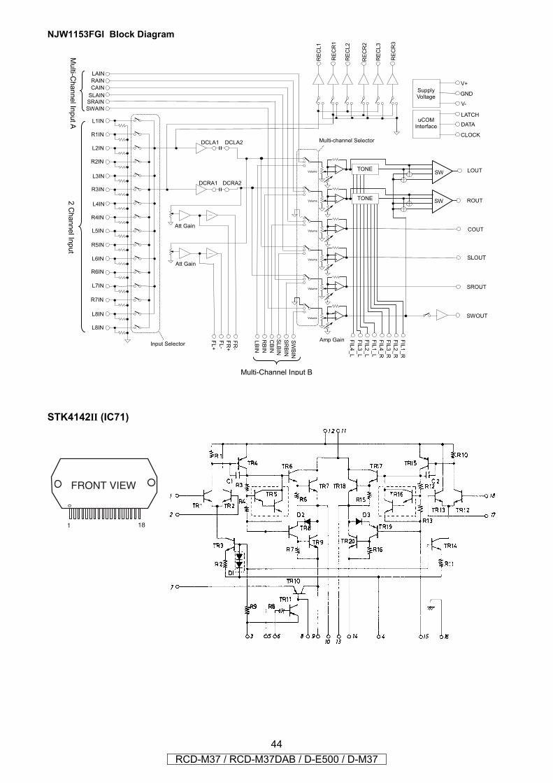
NJW1153FGI Block Diagram
STK4142II (IC71)
R1IN
FL
+
FL
-
LB
IN
RB
IN
CB
IN
SL
BIN
SR
BIN
SW
BIN
GND
V+
V-
LATCH
DATA
CLOCK
SupplyVoltage
uCOM Interface
FR
+
FR
-
Amp Gain
LOUT
ROUT
COUT
SLOUT
SROUT
SWOUT R
EC
L1
RE
CL
2
RE
CL
3
RE
CR
1
RE
CR
2
RE
CR
3
L1IN
L2IN
L3IN
L4IN
L5IN
L6IN
L7IN
L8IN
R2IN
R3IN
R4IN
R5IN
R6IN
R7IN
L8IN
LAIN
RAIN
CAIN
SLAIN SRAIN
SWAIN
Att Gain
Att Gain
DCLA1
SW
SW
VolumeTONE
TONE Volume
Volume
Volume
Volume
Volume
FIL
1_
R
FIL
2_
R
FIL
3_
R
FIL
4_
R
FIL
1_
L
FIL
2_
L
FIL
3_
L
FIL
4_
L
DCLA2
DCRA1 DCRA2
Multi-Channel Input B
Multi-C
hannel In
put A
2 C
hannel In
put
Input Selector
Multi-channel Selector
1 18
FRONT VIEW
44RCD-M37 / RCD-M37DAB / D-E500 / D-M37
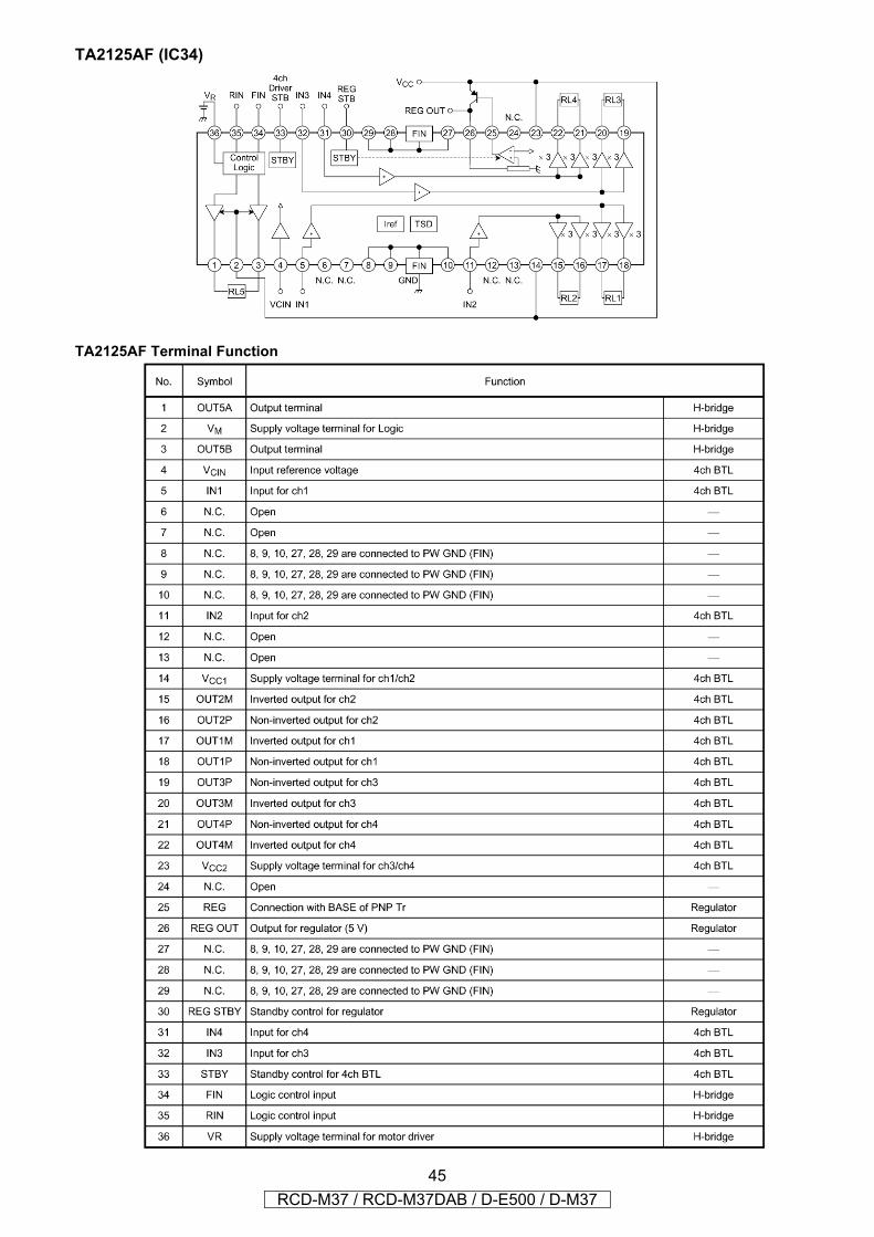
TA2125AF (IC34)
TA2125AF Terminal Function
45RCD-M37 / RCD-M37DAB / D-E500 / D-M37
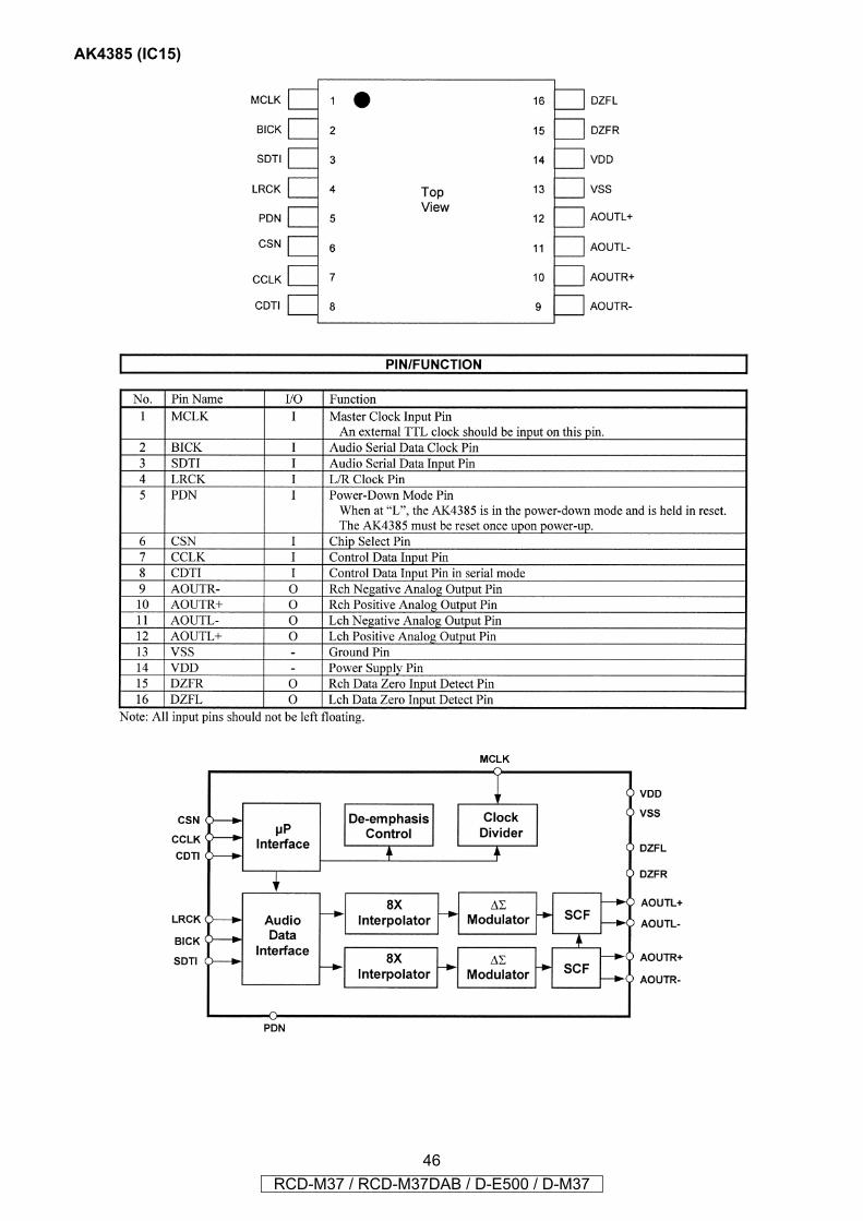
AK4385 (IC15)
46RCD-M37 / RCD-M37DAB / D-E500 / D-M37
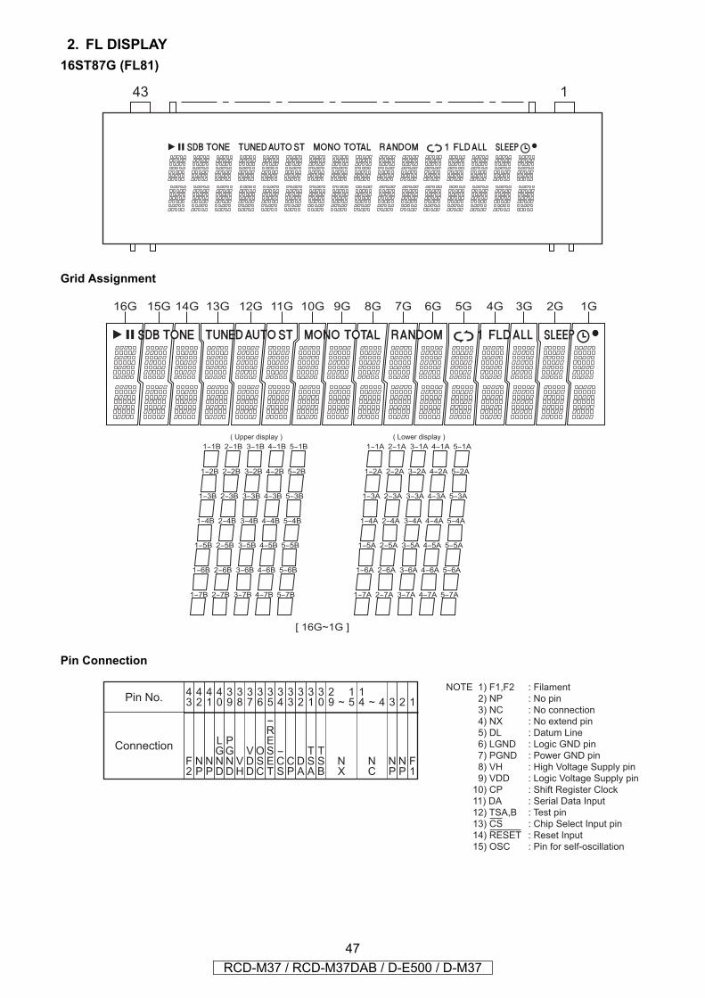
2. FL DISPLAY16ST87G (FL81)
Grid Assignment
Pin Connection
143
1-1B 2-1B 3-1B 4-1B 5-1B
1-2B 2-2B 3-2B 4-2B 5-2B
1-3B 2-3B 3-3B 4-3B 5-3B
1-4B 2-4B 3-4B 4-4B 5-4B
1-5B 2-5B 3-5B 4-5B 5-5B
1-6B 2-6B 3-6B 4-6B 5-6B
1-7B 2-7B 3-7B 4-7B 5-7B
[ 16G~1G ]
1-1A 2-1A 3-1A 4-1A 5-1A
1-2A 2-2A 3-2A 4-2A 5-2A
1-3A 2-3A 3-3A 4-3A 5-3A
1-4A 2-4A 3-4A 4-4A 5-4A
1-5A 2-5A 3-5A 4-5A 5-5A
1-6A 2-6A 3-6A 4-6A 5-6A
1-7A 2-7A 3-7A 4-7A 5-7A
16G 15G 14G 13G 12G 11G 10G 9G 8G 7G 6G 5G 4G 3G 2G 1G
( Upper display ) ( Lower display )
4~
N
C
~
N
X
3
N
P
2
N
P
1
F
1
4
0
L
G
N
D
3
9
P
G
N
D
3
7
V
D
D
3
4
-
C
S
3
6
O
S
C
3
5
-
R
E
S
E
T
3
1
T
S
A
3
0
T
S
B
2
9
1
5
1
4
4
3
F
2
4
2
N
P
4
1
N
P
3
2
D
A
3
3
C
P
3
8
V
H
Pin No.
Connection
NOTE 1) F1,F2 : Filament
2) NP : No pin
3) NC : No connection
4) NX : No extend pin
5) DL : Datum Line
6) LGND : Logic GND pin
7) PGND : Power GND pin
8) VH : High Voltage Supply pin
9) VDD : Logic Voltage Supply pin
10) CP : Shift Register Clock
11) DA : Serial Data Input
12) TSA,B : Test pin
13) CS : Chip Select Input pin
14) RESET : Reset Input
15) OSC : Pin for self-oscillation
47RCD-M37 / RCD-M37DAB / D-E500 / D-M37
---MEMO---
48RCD-M37 / RCD-M37DAB / D-E500 / D-M37
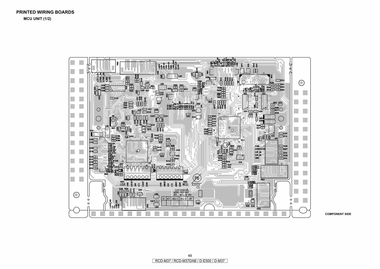
PRINTED WIRING BOARDSMCU UNIT (1/2)
COMPONENT SIDE
49RCD-M37 / RCD-M37DAB / D-E500 / D-M37
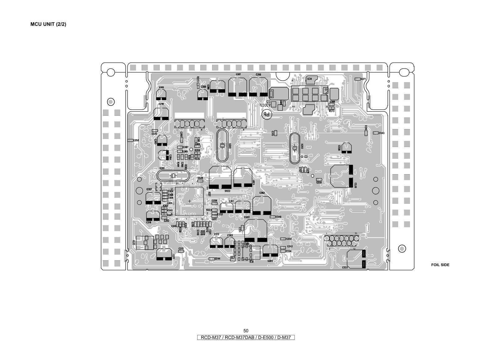
MCU UNIT (2/2)
FOIL SIDE
50RCD-M37 / RCD-M37DAB / D-E500 / D-M37
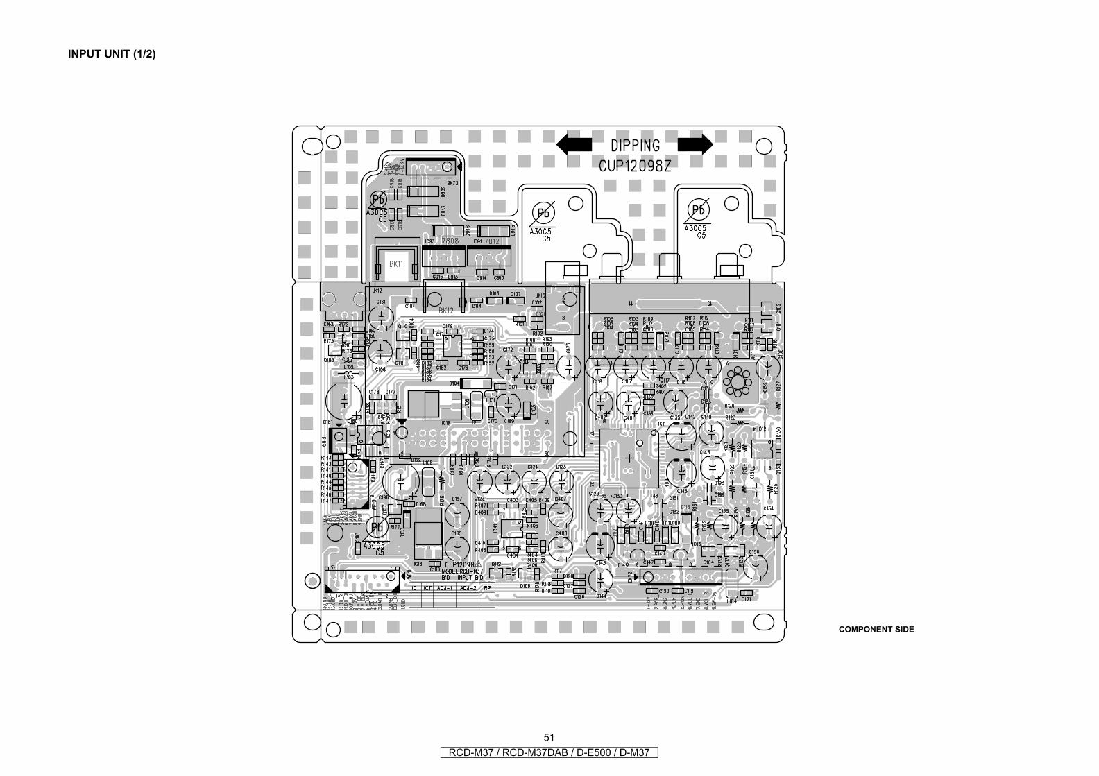
INPUT UNIT (1/2)
COMPONENT SIDE
51RCD-M37 / RCD-M37DAB / D-E500 / D-M37
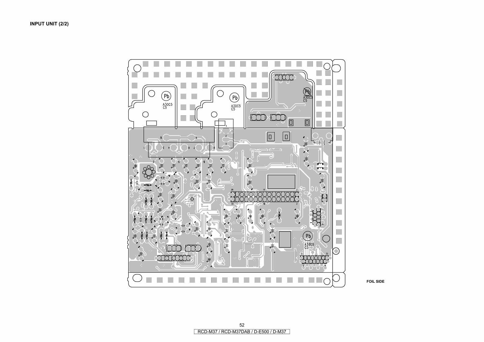
INPUT UNIT (2/2)
FOIL SIDE
52RCD-M37 / RCD-M37DAB / D-E500 / D-M37
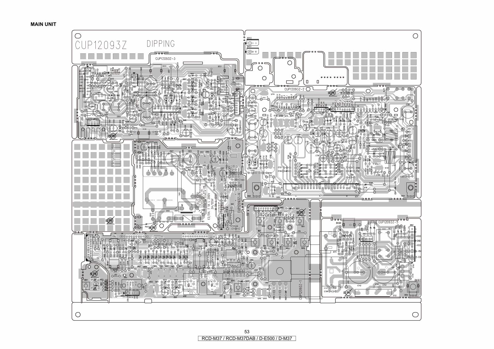
MAIN UNIT
53RCD-M37 / RCD-M37DAB / D-E500 / D-M37
---MEMO---
54RCD-M37 / RCD-M37DAB / D-E500 / D-M37
55RCD-M37 / RCD-M37DAB / D-E500 / D-M37
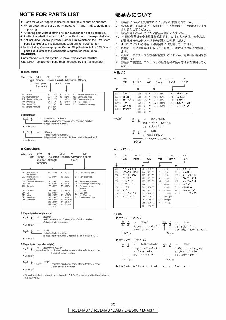
NOTE FOR PARTS LIST • Parts for which "nsp" is indicated on this table cannot be supplied. • When ordering of part, clearly indicate "1" and "I" (i) to avoid mis-
supplying. • Ordering part without stating its part number can not be supplied. • Part indicated with the mark "★ " is not illustrated in the exploded view. • Not including General-purpose Carbon Film Resistor in the P.W.Board
parts list. (Refer to the Schematic Diagram for those parts.) • Not including General-purpose Carbon Chip Resistor in the P.W.Board
parts list. (Refer to the Schematic Diagram for those parts.) WARNING: Parts marked with this symbol z have critical characteristics. Use ONLY replacement parts recommended by the manufacturer.
ss
ss
s s
s s
ss
ss
RD : 2B : 1/8 W F : ±1% P :RC : 2E : 1/4 W G : ±2% NL :RS : 2H : 1/2 W J : ±5% NB :RW : 3A : 1 W K : ±10% FR :RN : 3D : 2 W M : ±20% F :RK : 3F : 3 W
3H : 5 W
RN 14K 2E 182 G FR
∗ 18 2 1800 =1.8k
0
2
1R 2 1.2
1
2 R
CE 04W 1H 2R2 M BP
CE : 0J : 6.3 V F : ±1% HS :
CA : 1A : 10 V G : ±2% BP :CS : 1C : 16 V J : ±5% HR :CQ : 1E : 25 V K : ±10% DL :CK : 1V : 35 V M : ±20% HF :CC : 1H : 50 V Z : +80% U : ULCP : 2A : 100 V −20% C : CSACM : 2B : 125 V P : +100% W : UL-CSACF : 2C : 160 V − 0% F :CH : 2D : 200 V C : ±0.25pF
2E : 250 V D : ±0.5pF2H : 500 V = :
2J : 630 V
∗
22 2 2200μF
02
μF
22 2 2200pF=0.0022μF
0
2
pF pF
22 1 220pF
2
(0 2 )0
(0 0 1 )
2R 2 2.2μF
12 R
μF
AC
RD : Carbon 2B : 1/8W F : ±1% P : Pulse-resistant typeRC : Composition 2E : 1/4W G : ±2% NL : Low noise typeRS : Metal oxide film 2H : 1/2W J : ±5% NB : Non-burning typeRW : Winding 3A : 1W K : ±10% FR : Fuse-resistorRN : Metal film 3D : 2W M : ±20% F : Lead wire formingRK : Metal mixture 3F : 3W
3H : 5W
CE : Aluminum foil 0J : 6.3V F : ±1% HS : High stability typeelectrolytic
CA : Aluminum solid 1A : 10V G : ±2% BP : Non-polar typeelectrolytic
CS : Tantalum electrolytic 1C : 16V J : ±5% HR : Ripple-resistant typeCQ : Film 1E : 25V K : ±10% DL : For change and dischargeCK : Ceramic 1V : 35V M : ±20% HF : For assuring high
requencyCC : Ceramic 1H : 50V Z : +80% U : UL partCP : Oil 2A : 100V –20% C : CSA partCM : Mica 2B : 125V P : +100% W : UL-CSA typeCF : Metallized 2C : 160V –0% F : Lead wire formingCH : Metallized 2D : 200V C : ±0.25pF
2E : 250V D : ±0.5pF2H : 500V = : Others2J : 630V
lllll Resistors
Ex.: RN 14K 2E 182 G FRType Shape Power Resist- Allowable Others
and per- ance errorformance
] Resistance
1 8 2 ⇒ 1800 ohm = 1.8 kohmIndicates number of zeros after effective number.2-digit effective number.
• Units: ohm
1 R 2 ⇒ 1.2 ohm1-digit effective number.2-digit effective number, decimal point indicated by R.
• Units: ohm
lllll Capacitors
Ex.: CE 04W 1H 2R2 M BPType Shape Dielectric Capacity Allowable Others
and per- strength errorformance
] Capacity (electrolyte only)
2 2 2 ⇒ 2200μFIndicates number of zeros after effective number.2-digit effective number.
• Units: μF.
2 R 2 ⇒ 2.2μF1-digit effective number.2-digit effective number, decimal point indicated by R.
• Units: μF.
] Capacity (except electrolyte)
2 2 2 ⇒ 2200pF=0.0022μF(More than 2) Indicates number of zeros after effective number.
2-digit effective number.• Units: pF.
2 2 1 ⇒ 220pF(0 or 1) Indicates number of zeros after effective number.
2-digit effective number.• Units: pF.
• When the dielectric strength is indicated in AC, "AC" is included after the dieelectricstrength value.
部品表について1.部品表に "nsp" と記載されている部品は供給できません。2.部品を発注する際は特に数字の "1 " と英字の "I" との区別をはっきり記入してください。
3.部品番号を表示していない部品は供給できません。4. z印の部品は安全上重要な部品です。交換するときは、安全および性能維持のため必ず指定の部品をご使用ください。
5.★印のついている部品は分解図中には記載していません。6.汎用カーボン抵抗器は記載していません。定数は回路図を参照願います。
7.汎用カーボンチップ抵抗器は記載していません。定数は回路図を参照願います。
8.部品表の抵抗器、コンデンサの品名記号の読み方は表を参照してください。
PARTS LIST OF P.W.B. UNIT* 本表に "nsp" と記載されている部品は供給できません。* Parts for which "nsp" is indicated on this table cannot be supplied.\
* 本表に記載されている部品は、補修用部品のため製品に使用している部品とは一部、形状、寸法などが異なる場合があります。* The parts listed below are for maintenance only, might differ from the parts used in the unit in appearances or dimensions.
Note: The symbols in the column "Remarks" indicate the following destinations.E3 : U.S.A. & Canada mode E2 : Europe model EK : U.K. model JP : Japan model
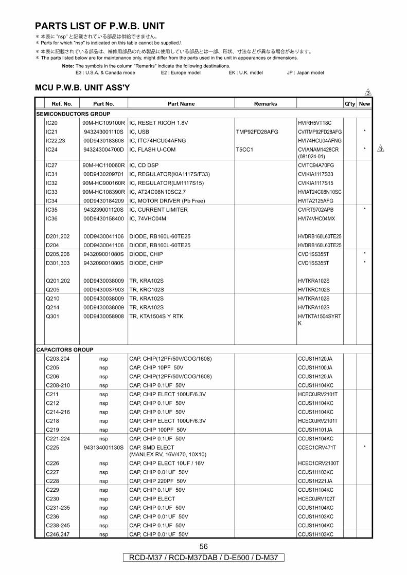
MCU P.W.B. UNIT ASS'Y
Ref. No. Part No. Part Name Remarks Q'ty New
SEMICONDUCTORS GROUPIC20 90M-HC109100R IC, RESET RICOH 1.8V HVIRH5VT18CIC21 943243001110S IC, USB TMP92FD28AFG CVITMP92FD28AFG *IC22,23 00D9430183608 IC, ITC74HCU04AFNG HVI74HCU04AFNGIC24 943243004700D IC, FLASH U-COM T5CC1 CVIANAM1428CR
(081024-01)*
IC27 90M-HC110060R IC, CD DSP CVITC94A70FGIC31 00D9430209701 IC, REGULATOR(KIA1117S/F33) CVIKIA1117S33IC32 90M-HC900160R IC, REGULATOR(LM1117S15) CVIKIA1117S15IC33 90M-HC108390R IC, AT24C08N10SC2.7 HVIAT24C08N10SCIC34 00D9430184209 IC, MOTOR DRIVER (Pb Free) HVITA2125AFGIC35 943239001120S IC, CURRENT LIMITER CVIRT9702APB *IC36 00D9430158400 IC, 74VHC04M HVI74VHC04MX
D201,202 00D9430041106 DIODE, RB160L-60TE25 HVDRB160L60TE25D204 00D9430041106 DIODE, RB160L-60TE25 HVDRB160L60TE25D205,206 943209001080S DIODE, CHIP CVD1SS355T *D301,303 943209001080S DIODE, CHIP CVD1SS355T *
Q201,202 00D9430038009 TR, KRA102S HVTKRA102SQ205 00D9430037903 TR, KRC102S HVTKRC102SQ210 00D9430038009 TR, KRA102S HVTKRA102SQ214 00D9430038009 TR, KRA102S HVTKRA102SQ301 00D9430058908 TR, KTA1504S Y RTK HVTKTA1504SYRT
K
CAPACITORS GROUPC203,204 nsp CAP, CHIP(12PF/50V/COG/1608) CCUS1H120JAC205 nsp CAP, CHIP 10PF 50V CCUS1H100JAC206 nsp CAP, CHIP(12PF/50V/COG/1608) CCUS1H120JAC208-210 nsp CAP, CHIP 0.1UF 50V CCUS1H104KCC211 nsp CAP, CHIP ELECT 100UF/6.3V HCEC0JRV2101TC212 nsp CAP, CHIP 0.1UF 50V CCUS1H104KCC214-216 nsp CAP, CHIP 0.1UF 50V CCUS1H104KCC218 nsp CAP, CHIP ELECT 100UF/6.3V HCEC0JRV2101TC219 nsp CAP, CHIP 100PF 50V CCUS1H101JAC221-224 nsp CAP, CHIP 0.1UF 50V CCUS1H104KCC225 943134001130S CAP, SMD ELECT
(MANLEX RV, 16V/470, 10X10) CCEC1CRV471T *
C226 nsp CAP, CHIP ELECT 10UF / 16V HCEC1CRV2100TC227 nsp CAP, CHIP 0.01UF 50V CCUS1H103KCC228 nsp CAP, CHIP 220PF 50V CCUS1H221JAC229 nsp CAP, CHIP 0.1UF 50V CCUS1H104KCC230 nsp CAP, CHIP ELECT HCEC0JRV102TC231-235 nsp CAP, CHIP 0.1UF 50V CCUS1H104KCC236 nsp CAP, CHIP 0.01UF 50V CCUS1H103KCC238-245 nsp CAP, CHIP 0.1UF 50V CCUS1H104KCC246,247 nsp CAP, CHIP 0.01UF 50V CCUS1H103KC
d
d
56RCD-M37 / RCD-M37DAB / D-E500 / D-M37
C248-250 nsp CAP, CHIP 0.1UF 50V CCUS1H104KCC252,253 nsp CAP, CHIP 0.1UF 50V CCUS1H104KCC301 nsp CAP, CHIP 0.1UF 50V CCUS1H104KCC302 nsp CAP, CHIP 1000PF 50V CCUS1H102KCC303,304 nsp CAP, CHIP 0.1UF 50V CCUS1H104KCC306 nsp CAP, CHIP 0.1UF 50V CCUS1H104KCC307 nsp CAP, CHIP ELECT 100UF/6.3V HCEC0JRV2101TC308-312 nsp CAP, CHIP 0.1UF 50V CCUS1H104KCC313 nsp CAP, CHIP ELECT 47UF/6.3V HCEC0JRV2470TC315 nsp CAP, CHIP 0.1UF 50V CCUS1H104KCC316,317 nsp CAP, CHIP ELECT 47UF/6.3V HCEC0JRV2470TC318 nsp CAP, CHIP 0.1UF 50V CCUS1H104KCC319 nsp CAP, CHIP 0.033UF 50V CCUS1H333KCC320 nsp CAP, CHIP 47PF 50V CCUS1H470JAC321 nsp CAP, CHIP 0.015UF 50V CCUS1H153KCC322,323 nsp CAP, CHIP 0.01UF 50V CCUS1H103KCC324 nsp CAP, CHIP 4700PF 50V CCUS1H472KCC325 nsp CAP, CHIP 0.1UF 50V CCUS1H104KCC326 nsp CAP, CHIP 0.01UF 50V CCUS1H103KCC327 nsp CAP, CHIP 0.1UF 50V CCUS1H104KCC328 nsp CAP, CHIP 0.015UF 50V CCUS1H153KCC329 nsp CAP, CHIP 0.1UF 50V CCUS1H104KCC330 nsp CAP, CHIP 68PF 50V CCUS1H680JAC331 nsp CAP, CHIP 0.1UF 50V CCUS1H104KCC332 nsp CAP, CHIP ELECT HCEC0JRV102TC333 nsp CAP, CHIP 1000PF 50V CCUS1H102KCC334 nsp CAP, CHIP 0.01UF 50V CCUS1H103KCC335 nsp CAP, CHIP ELECT HCEC0JRV102TC336,337 nsp CAP, CHIP 470PF 50V CCUS1H471JAC338 nsp CAP, CHIP 0.1UF 50V CCUS1H104KCC339,340 nsp CAP, CHIP 0.033UF 50V CCUS1H333KCC341 nsp CAP, CHIP 0.1UF 50V CCUS1H104KCC342,343 nsp CAP, CHIP 0.047UF 50V CCUS1H473KCC344 nsp CAP, CHIP 2200PF 50V CCUS1H222KCC345-349 nsp CAP, CHIP 0.1UF 50V CCUS1H104KCC350,351 nsp CAP, CHIP(12PF/50V/COG/1608)
12PF 50VCCUS1H120JA
C352 nsp CAP, CHIP ELECT 100UF/6.3V HCEC0JRV2101TC353 nsp CAP, CHIP 0.1UF 50V CCUS1H104KCC354-359 nsp CAP, CHIP 22PF 50V CCUS1H220JAC361,362 nsp CAP, CHIP ELECT HCEC0JRV471TC365 nsp CAP, CHIP 0.1UF 50V CCUS1H104KCC366 943134001130S CAP, SMD ELECT
(MANLEX RV, 16V/470, 10X10) CCEC1CRV471T *
C367,368 nsp CAP, CHIP 0.01UF 50V CCUS1H103KCC369 nsp CAP, CHIP 0.1UF 50V CCUS1H104KCC370 nsp CAP, CHIP 1000PF 50V CCUS1H102KCC371 nsp CAP, CHIP 0.1UF 50V CCUS1H104KCC372,373 nsp CAP, CHIP 68PF 50V CCUS1H680JAC377 nsp CAP, CHIP 470PF 50V CCUS1H471JAC378,379 nsp CAP, CHIP(18PF/50V) 18PF 50V CCUS1H180JAC380-382 nsp CAP, CHIP 0.1UF 50V CCUS1H104KCC383,384 nsp CAP, CHIP ELECT 10UF / 16V HCEC1CRV2100TC385-387 nsp CAP, CHIP 0.1UF 50V CCUS1H104KCC388 nsp CAP, CHIP ELECT 100UF/6.3V HCEC0JRV2101TC389,390 nsp CAP, CHIP ELECT 10UF / 16V HCEC1CRV2100TC391 nsp CAP, CHIP 1UF 10V CCUS1A105KC
Ref. No. Part No. Part Name Remarks Q'ty New
57RCD-M37 / RCD-M37DAB / D-E500 / D-M37
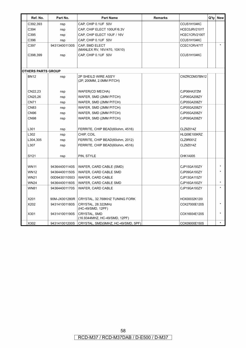
C392,393 nsp CAP, CHIP 0.1UF 50V CCUS1H104KCC394 nsp CAP, CHIP ELECT 100UF/6.3V HCEC0JRV2101TC395 nsp CAP, CHIP ELECT 10UF / 16V HCEC1CRV2100TC396 nsp CAP, CHIP 0.1UF 50V CCUS1H104KCC397 943134001130S CAP, SMD ELECT
(MANLEX RV, 16V/470, 10X10) CCEC1CRV471T *
C398,399 nsp CAP, CHIP 0.1UF 50V CCUS1H104KC
OTHERS PARTS GROUPBN12 nsp 2P SHEILD WIRE ASS'Y
(2P, 200MM, 2.0MM PITCH) CWZRCDM37BN12
CN22,23 nsp WAFER(CD MECHA) CJP06HA37ZMCN25,26 nsp WAFER, SMD (2MM PITCH) CJP06GA208ZYCN71 nsp WAFER, SMD (2MM PITCH) CJP05GA208ZYCN83 nsp WAFER, SMD (2MM PITCH) CJP05GA208ZYCN96 nsp WAFER, SMD (2MM PITCH) CJP05GA208ZYCN98 nsp WAFER, SMD (2MM PITCH) CJP09GA208ZY
L301 nsp FERRITE, CHIP BEAD(60ohm, 4516) CLZ9Z014ZL302 nsp CHIP, COIL HLQ09E100KRZL304,305 nsp FERRITE, CHIP BEAD(60ohm, 2012) CLZ9R001ZL307 nsp FERRITE, CHIP BEAD(60ohm, 4516) CLZ9Z014Z
SY21 nsp PIN, STYLE CHK1A005
WN11 943644001140S WAFER, CARD CABLE (SMD) CJP15GA193ZY *WN12 943644001150S WAFER, CARD CABLE SMD CJP09GA193ZY *WN21 00D9430110503 WAFER, CARD CABLE CJP13GA115ZYWN24 943644001160S WAFER, CARD CABLE SMD CJP16GA193ZY *WN81 943644001170S WAFER, CARD CABLE CJP19GA193ZY *
X201 90M-JX001280R CRYSTAL, 32.768KHZ TUNING FORK HOX00032K120IX202 943141001180S CRYSTAL, 28.322MHz
(HC-49/SMD, 12PF)COX27000E120S *
X301 943141001190S CRYSTAL, SMD(16.9344MHZ, HC-49/SMD, 12PF)
COX16934E120S *
X302 943141001200S CRYSTAL, SMD(9MHZ, HC-49/SMD, 5PF) COX09000E150S *
Ref. No. Part No. Part Name Remarks Q'ty New
58RCD-M37 / RCD-M37DAB / D-E500 / D-M37
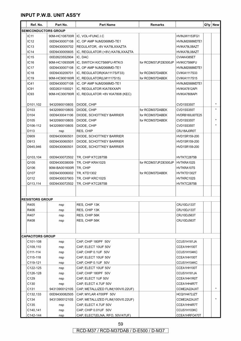
INPUT P.W.B. UNIT ASS'Y
Ref. No. Part No. Part Name Remarks Q'ty New
SEMICONDUCTORS GROUPIC11 90M-HC108700R IC, VOL+FUNC.I.C HVINJW1153FG1IC12 00D9430007108 IC, OP AMP NJM2068MD-TE1 HVINJM2068MDTE1IC13 00D9430005702 REGULATOR, -8V KA79LXXAZTA HVIKA79L08AZTIC14 00D9430005605 IC, REGULATOR (+8V) KA78LXXAZTA HVIKA78L08AZTIC15 00D2623552904 IC, DAC CVIAK4385ETIC16 90M-HC109350R IC, SWITCH KIC7S66FU-RTK/3 for RCDM37JP,DE500JP HVIKIC7S66FUIC17 00D9430007108 IC, OP AMP NJM2068MD-TE1 HVINJM2068MDTE1IC18 00D9430209701 IC, REGULATOR(KIA1117S/F33) for RCDM37DABEK CVIKIA1117S33IC19 90M-HC900160R IC, REGULATOR(LM1117S15) for RCDM37DABEK CVIKIA1117S15IC41 00D9430007108 IC, OP AMP NJM2068MD-TE1 HVINJM2068MDTE1IC91 00D2631100021 IC, REGULATOR KIA78XXAPI HVIKIA7812APIIC93 90M-HC300780R IC, REGULATOR +8V KIA7808 (KEC) HVIKIA7808API
D101,102 943209001080S DIODE, CHIP CVD1SS355T *D103 943209001080S DIODE, CHIP for RCDM37DABEK CVD1SS355T *D104 00D9430041106 DIODE, SCHOTTKEY BARRIER for RCDM37DABEK HVDRB160L60TE25D105 943209001080S DIODE, CHIP for RCDM37DABEK CVD1SS355T *D106-112 943209001080S DIODE, CHIP CVD1SS355T *D113 nsp RES, CHIP CRJ18AJ0R0TD909 00D9430060501 DIODE, SCHOTTKEY BARRIER HVD1SR159-200D913 00D9430060501 DIODE, SCHOTTKEY BARRIER HVD1SR159-200D945,946 00D9430060501 DIODE, SCHOTTKEY BARRIER HVD1SR159-200
Q103,104 00D9430072502 TR, CHIP KTC2875B HVTKTC2875BQ105 00D9430038009 TR, CHIP KRA102S for RCDM37JP,DE500JP HVTKRA102SQ106 90M-BA001600R TR, CHIP HVTKRA107SQ107 00D9430006002 TR, KTD1302 for RCDM37DABEK HVTKTD1302TQ112 00D9430037903 TR, CHIP KRC102S HVTKRC102SQ113,114 00D9430072502 TR, CHIP KTC2875B HVTKTC2875B
RESISTORS GROUPR405 nsp RES, CHIP 13K CRJ10DJ133TR406 nsp RES, CHIP 13K CRJ10DJ133TR407 nsp RES, CHIP 56K CRJ10DJ563TR408 nsp RES, CHIP 56K CRJ10DJ563T
CAPACITORS GROUPC101-108 nsp CAP, CHIP 180PF 50V CCUS1H181JAC109,110 nsp CAP, ELECT 10UF 50V CCEA1HH100TC111-114 nsp CAP, CHIP 0.1UF 50V CCUS1H104KCC115-118 nsp CAP, ELECT 10UF 50V CCEA1HH100TC119-121 nsp CAP, CHIP 0.1UF 50V CCUS1H104KCC122-125 nsp CAP, ELECT 10UF 50V CCEA1HH100TC126-128 nsp CAP, CHIP 180PF 50V CCUS1H181JAC129 nsp CAP, ELECT 1UF 50V CCEA1HH1R0TC130 nsp CAP, ELECT 4.7UF 50V CCEA1HH4R7TC131 943139001210S CAP, METALLIZED FLIM(100V/0.22UF) CCME2A224JXT *C132,133 00D9430082505 CAP, MYLAR 4700PF 50V HCQI1H472JZTC134 943139001210S CAP, METALLIZED FLIM(100V/0.22UF) CCME2A224JXT *C135 nsp CAP, ELECT 4.7UF 50V CCEA1HH4R7TC140,141 nsp CAP, CHIP 0.01UF 50V CCUS1H103KCC142-144 nsp CAP, ELECT(ELNA, RFO, 50V/47UF) CCEA1HRFO470T
59RCD-M37 / RCD-M37DAB / D-E500 / D-M37
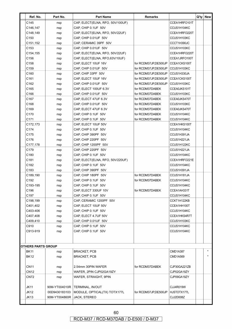
C145 nsp CAP, ELECT(ELNA, RFO, 50V/100UF) CCEA1HRFO101TC146,147 nsp CAP, CHIP 0.1UF 50V CCUS1H104KCC148,149 nsp CAP, ELECT(ELNA, RFO, 50V/22UF) CCEA1HRFO220TC150 nsp CAP, CHIP 0.01UF 50V CCUS1H103KCC151,152 nsp CAP, CERAMIC 39PF 50V CCCT1H390JCC153 nsp CAP, CHIP 0.01UF 50V CCUS1H103KCC154,155 nsp CAP, ELECT(ELNA, RFO, 50V/22UF) CCEA1HRFO220TC156 nsp CAP, ELECT(ELNA, RFO,63V/10UF) CCEA1JRFO100TC158 nsp CAP, ELECT 10UF 16V for RCDM37JP,DE500JP CCEA1CKS100TC159 nsp CAP, CHIP 0.01UF 50V for RCDM37JP,DE500JP CCUS1H103KCC160 nsp CAP, CHIP 33PF 50V for RCDM37JP,DE500JP CCUS1H330JAC161 nsp CAP, ELECT 10UF 16V for RCDM37JP,DE500JP CCEA1CKS100TC162 nsp CAP, CHIP 0.01UF 50V for RCDM37JP,DE500JP CCUS1H103KCC165 nsp CAP, ELECT 100UF 6.3V for RCDM37DABEK CCEA0JKS101TC166 nsp CAP, CHIP 0.01UF 50V for RCDM37DABEK CCUS1H103KCC167 nsp CAP, ELECT 47UF 6.3V for RCDM37DABEK CCEA0JKS470TC168 nsp CAP, CHIP 0.01UF 50V for RCDM37DABEK CCUS1H103KCC169 nsp CAP, ELECT 47UF 6.3V for RCDM37DABEK CCEA0JKS470TC170 nsp CAP, CHIP 0.1UF 50V for RCDM37DABEK CCUS1H104KCC171 nsp CAP, CHIP 0.1UF 50V for RCDM37DABEK CCUS1H104KCC172,173 nsp CAP, ELECT 10UF 50V CCEA1HKS100TC174 nsp CAP, CHIP 0.1UF 50V CCUS1H104KCC175 nsp CAP, CHIP 390PF 50V CCUS1H391JAC176 nsp CAP, CHIP 220PF 50V CCUS1H221JAC177,178 nsp CAP, CHIP 1200PF 50V CCUS1H122KCC179 nsp CAP, CHIP 220PF 50V CCUS1H221JAC180 nsp CAP, CHIP 0.1UF 50V CCUS1H104KCC181 nsp CAP, ELECT(ELNA, RFO, 50V/220UF) CCEA1HRFO221EC182 nsp CAP, CHIP 0.1UF 50V CCUS1H104KCC183 nsp CAP, CHIP 390PF 50V CCUS1H391JAC189,190 nsp CAP, CHIP 180PF 50V for RCDM37DABEK CCUS1H181JAC192 nsp CAP, CHIP 0.1UF 50V for RCDM37DABEK CCUS1H104KCC193-195 nsp CAP, CHIP 0.1UF 50V CCUS1H104KCC196 nsp CAP, ELECT 330UF 10V for RCDM37DABEK CCEA1AH331TC197 nsp CAP, CHIP 0.1UF 50V CCUS1H104KCC198,199 nsp CAP, CERAMIC 1200PF 50V CCKT1H122KBC401,402 nsp CAP, ELECT 10UF 50V CCEA1HH100TC403-406 nsp CAP, CHIP 0.1UF 50V CCUS1H104KCC407,408 nsp CAP, ELECT 4.7UF 50V CCEA1HKS4R7TC409,410 nsp CAP, CHIP 0.01UF 50V CCUS1H103KCC910 nsp CAP, CHIP 0.1UF 50V CCUS1H104KCC913-919 nsp CAP, CHIP 0.1UF 50V CCUS1H104KC
OTHERS PARTS GROUPBK11 nsp BRACKET, PCB CMD1A387 *BK12 nsp BRACKET, PCB CMD1A569 *
CN11 nsp 2.54mm 30PIN WAFER for RCDM37DABEK CJP30GA221ZBCN12 nsp WAFER, 2PIN CJP02GA19ZY CJP02GA19ZYCN72 nsp WAFER, STRAIGHT, 9PIN CJP09GA19ZY
JK11 90M-YT004010R TERMINAL, IN/OUT CJJ4R019WJK12 00D9430183103 MODULE, OPTICAL(TX) TOTX177L for RCDM37JP,DE500JP HJSTOTX177LJK13 90M-YT004860R JACK, STEREO CJJ2D008Z
Ref. No. Part No. Part Name Remarks Q'ty New
60RCD-M37 / RCD-M37DAB / D-E500 / D-M37
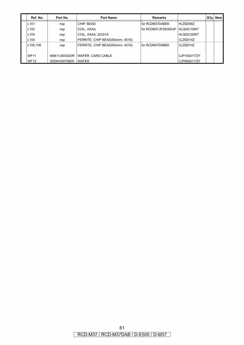
L101 nsp CHIP, BEAD for RCDM37DABEK HLZ9Z008ZL102 nsp COIL, AXAIL for RCDM37JP,DE500JP HLQ02C100KTL103 nsp COIL, AXAIL 22UH,K HLQ02C220KTL104 nsp FERRITE, CHIP BEAD(60ohm, 4516) CLZ9Z014ZL105,106 nsp FERRITE, CHIP BEAD(60ohm, 4516) for RCDM37DABEK CLZ9Z014Z
WF11 90M-YJ003020R WAFER, CARD CABLE CJP15GA117ZYWF12 00D9430076605 WAFER CJP09GA117ZY
Ref. No. Part No. Part Name Remarks Q'ty New
61RCD-M37 / RCD-M37DAB / D-E500 / D-M37
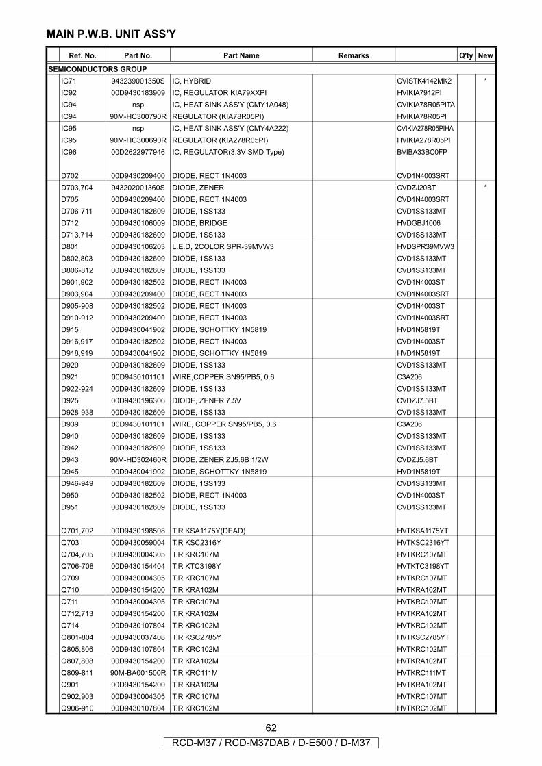
MAIN P.W.B. UNIT ASS'Y
Ref. No. Part No. Part Name Remarks Q'ty New
SEMICONDUCTORS GROUPIC71 943239001350S IC, HYBRID CVISTK4142MK2 *IC92 00D9430183909 IC, REGULATOR KIA79XXPI HVIKIA7912PIIC94 nsp IC, HEAT SINK ASS'Y (CMY1A048) CVIKIA78R05PITAIC94 90M-HC300790R REGULATOR (KIA78R05PI) HVIKIA78R05PIIC95 nsp IC, HEAT SINK ASS'Y (CMY4A222) CVIKIA278R05PIHAIC95 90M-HC300690R REGULATOR (KIA278R05PI) HVIKIA278R05PIIC96 00D2622977946 IC, REGULATOR(3.3V SMD Type) BVIBA33BC0FP
D702 00D9430209400 DIODE, RECT 1N4003 CVD1N4003SRTD703,704 943202001360S DIODE, ZENER CVDZJ20BT *D705 00D9430209400 DIODE, RECT 1N4003 CVD1N4003SRTD706-711 00D9430182609 DIODE, 1SS133 CVD1SS133MTD712 00D9430106009 DIODE, BRIDGE HVDGBJ1006D713,714 00D9430182609 DIODE, 1SS133 CVD1SS133MTD801 00D9430106203 L.E.D, 2COLOR SPR-39MVW3 HVDSPR39MVW3D802,803 00D9430182609 DIODE, 1SS133 CVD1SS133MTD806-812 00D9430182609 DIODE, 1SS133 CVD1SS133MTD901,902 00D9430182502 DIODE, RECT 1N4003 CVD1N4003STD903,904 00D9430209400 DIODE, RECT 1N4003 CVD1N4003SRTD905-908 00D9430182502 DIODE, RECT 1N4003 CVD1N4003STD910-912 00D9430209400 DIODE, RECT 1N4003 CVD1N4003SRTD915 00D9430041902 DIODE, SCHOTTKY 1N5819 HVD1N5819TD916,917 00D9430182502 DIODE, RECT 1N4003 CVD1N4003STD918,919 00D9430041902 DIODE, SCHOTTKY 1N5819 HVD1N5819TD920 00D9430182609 DIODE, 1SS133 CVD1SS133MTD921 00D9430101101 WIRE,COPPER SN95/PB5, 0.6 C3A206D922-924 00D9430182609 DIODE, 1SS133 CVD1SS133MTD925 00D9430196306 DIODE, ZENER 7.5V CVDZJ7.5BTD928-938 00D9430182609 DIODE, 1SS133 CVD1SS133MTD939 00D9430101101 WIRE, COPPER SN95/PB5, 0.6 C3A206D940 00D9430182609 DIODE, 1SS133 CVD1SS133MTD942 00D9430182609 DIODE, 1SS133 CVD1SS133MTD943 90M-HD302460R DIODE, ZENER ZJ5.6B 1/2W CVDZJ5.6BTD945 00D9430041902 DIODE, SCHOTTKY 1N5819 HVD1N5819TD946-949 00D9430182609 DIODE, 1SS133 CVD1SS133MTD950 00D9430182502 DIODE, RECT 1N4003 CVD1N4003STD951 00D9430182609 DIODE, 1SS133 CVD1SS133MT
Q701,702 00D9430198508 T.R KSA1175Y(DEAD) HVTKSA1175YTQ703 00D9430059004 T.R KSC2316Y HVTKSC2316YTQ704,705 00D9430004305 T.R KRC107M HVTKRC107MTQ706-708 00D9430154404 T.R KTC3198Y HVTKTC3198YTQ709 00D9430004305 T.R KRC107M HVTKRC107MTQ710 00D9430154200 T.R KRA102M HVTKRA102MTQ711 00D9430004305 T.R KRC107M HVTKRC107MTQ712,713 00D9430154200 T.R KRA102M HVTKRA102MTQ714 00D9430107804 T.R KRC102M HVTKRC102MTQ801-804 00D9430037408 T.R KSC2785Y HVTKSC2785YTQ805,806 00D9430107804 T.R KRC102M HVTKRC102MTQ807,808 00D9430154200 T.R KRA102M HVTKRA102MTQ809-811 90M-BA001500R T.R KRC111M HVTKRC111MTQ901 00D9430154200 T.R KRA102M HVTKRA102MTQ902,903 00D9430004305 T.R KRC107M HVTKRC107MTQ906-910 00D9430107804 T.R KRC102M HVTKRC102MT
62RCD-M37 / RCD-M37DAB / D-E500 / D-M37
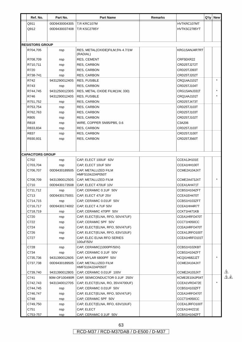
f
Q911 00D9430004305 T.R KRC107M HVTKRC107MTQ912 00D9430037408 T.R KSC2785Y HVTKSC2785YT
RESISTORS GROUPR704,705 nsp RES, METAL(OXIDE)FILM,5% 4.7/1W
(RADIAL)KRG1SANJ4R7RT
R708,709 nsp RES, CEMENT CRF5EKR22R710,711 nsp RES, CARBON CRD25TJ272TR720 nsp RES, CARBON CRD20TJ393TR738-741 nsp RES, CARBON CRD25TJ202TR742 943129001240S RES, FUSIBLE CRQ14AJ101T *R743 nsp RES, CARBON CRD25TJ104TR744,745 943125001230S RES, METAL OXIDE FILM(1W, 330) CRG1SANJ331T *R746 943129001240S RES, FUSIBLE CRQ14AJ101T *R751,752 nsp RES, CARBON CRD25TJ473TR753,754 nsp RES, CARBON CRD25TJ103TR762,763 nsp RES, CARBON CRD25TJ103TR805 nsp RES, CARBON CRD25TJ102TR818 nsp WIRE, COPPER SN95/PB5, 0.6 C3A206R833,834 nsp RES, CARBON CRD25TJ103TR837 nsp RES, CARBON CRD25TJ100TR930,931 nsp RES, CARBON CRD25TJ560T
CAPACITORS GROUPC702 nsp CAP, ELECT 100UF 63V CCEA1JH101EC703,704 nsp CAP, ELECT 10UF 50V CCEA1HH100TC706,707 00D9430189505 CAP, METALLIZED FILM
HMFS104J2AP050TCCME2A104JXT
C708,709 943139001250S CAP, METALLIZED FILM CCME2A473JXT *C710 00D9430173508 CAP, ELECT 470UF 10V CCEA1AH471TC711,712 nsp CAP, CERAMIC 0.1UF 50V CCBS1H104ZFTC713 00D9430175001 CAP, ELECT 47UF 25V CCEA1EH470TC714,715 nsp CAP, CERAMIC 0.01UF 50V CCBS1H103ZFTC716,717 00D9430174002 CAP, ELECT 4.7UF 50V CCEA1HH4R7TC718,719 nsp CAP, CERAMIC 470PF 50V CCKT1H471KBC720 nsp CAP, ELECT(ELNA, RFO, 50V/47UF) CCEA1HRFO470TC722 nsp CAP, CERAMIC 5PF 50V CCCT1H050CCC724 nsp CAP, ELECT(ELNA, RFO, 50V/47UF) CCEA1HRFO470TC726 nsp CAP, ELECT(ELNA, RFO, 63V/10UF) CCEA1JRFO100TC727 nsp CAP, ELEC ELNA RFO SERIES
100uF/50VCCEA1HRFO101T
C728 nsp CAP, CERAMIC(1000PF/50V) CCBS1H102KBTC734 nsp CAP, CERAMIC 0.1UF 50V CCBS1H104ZFTC735,736 943139001260S CAP, MYLAR 6800PF 50V HCQI1H682JZT *C737,738 00D9430189505 CAP, METALLIZED FILM
HMFS104J2AP050TCCME2A104JXT
C739,740 943139001280S CAP, CERAMIC 0.01UF 100V CCME2A103JXTC741 90M-OF100490R CAP, SEMICONDUCTOR 0.1UF 250V KCME2E104JP04TC742,743 943134001270S CAP, ELECT(ELNA, RO, 35V/4700UF) CCEA1VRO472E *C744,745 nsp CAP, CERAMIC 0.01UF 50V CCBS1H103ZFTC746,747 nsp CAP, ELECT(ELNA, RFO, 50V/47UF) CCEA1HRFO470TC748 nsp CAP, CERAMIC 5PF 50V CCCT1H050CCC749,750 nsp CAP, ELECT(ELNA, RFO, 63V/10UF) CCEA1JRFO100TC751 nsp CAP, ELECT CCEA1HH221EC753-757 nsp CAP, CERAMIC 0.1UF 50V CCBS1H104ZFT
Ref. No. Part No. Part Name Remarks Q'ty New
d
d
63RCD-M37 / RCD-M37DAB / D-E500 / D-M37
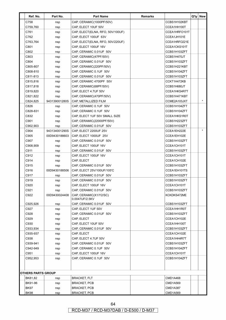
C758 nsp CAP, CERAMIC(1000PF/50V) CCBS1H102KBTC759,760 nsp CAP, ELECT 10UF 50V CCEA1HH100TC761 nsp CAP, ELECT(ELNA, RFO, 50V/100UF) CCEA1HRFO101TC762 nsp CAP, ELECT 100UF 63V CCEA1JH101EC763,764 nsp CAP, ELECT(ELNA, RFO, 50V/220UF) CCEA1HRFO221EC801 nsp CAP, ELECT 100UF 16V CCEA1CKS101TC802 nsp CAP, CERAMIC 0.01UF 50V CCBS1H103ZFTC803 nsp CAP, CERAMIC(47PF/50V) CCBS1H470JTC804 nsp CAP, CERAMIC 0.01UF 50V CCBS1H103ZFTC805-807 nsp CAP, CERAMIC(220PF/50V) CCBS1H221KBTC808-810 nsp CAP, CERAMIC 0.1UF 50V CCBS1H104ZFTC811-813 nsp CAP, CERAMIC 0.01UF 50V CCBS1H103ZFTC815,816 nsp CAP, CERAMIC 4700PF 50V CCKT1H472KBC817,818 nsp CAP, CERAMIC(68PF/50V) CCBS1H680JTC819,820 nsp CAP, ELECT 4.7UF 50V CCEA1HKS4R7TC821,822 nsp CAP, CERAMIC(470PF/50V) CCBS1H471KBTC824,825 943139001280S CAP, METALLIZED FILM CCME2A103JXT *C826 nsp CAP, CERAMIC 0.1UF 50V CCBS1H104ZFTC828-831 nsp CAP, CERAMIC 0.1UF 50V CCBS1H104ZFTC832 nsp CAP, ELECT 1UF 50V SMALL SIZE CCEA1HKS1R0TC901 nsp CAP, CERAMIC(22000PF/50V) CCBS1H223ZFTC902,903 nsp CAP, CERAMIC 0.01UF 50V CCBS1H103ZFTC904 943134001290S CAP, ELECT 2200UF 25V CCEA1EH222E *C905 00D9430188603 CAP, ELECT 1000UF 25V CCEA1EH102EC907 nsp CAP, CERAMIC 0.01UF 50V CCBS1H103ZFTC908,909 nsp CAP, ELECT 100UF 16V CCEA1CH101TC911 nsp CAP, CERAMIC 0.01UF 50V CCBS1H103ZFTC912 nsp CAP, ELECT 100UF 16V CCEA1CH101TC914 nsp CAP, ELECT CCEA1CH102EC915 nsp CAP, CERAMIC 0.01UF 50V CCBS1H103ZFTC916 00D9430188506 CAP, ELECT 25V/100UF/105'C CCEA1EH101TSC917 nsp CAP, CERAMIC 0.01UF 50V CCBS1H103ZFTC919 nsp CAP, CERAMIC 0.01UF 50V CCBS1H103ZFTC920 nsp CAP, ELECT 100UF 16V CCEA1CH101TC921 nsp CAP, CERAMIC 0.01UF 50V CCBS1H103ZFTC922 00D9430024408 CAP, CERAMIC(X1/Y2/SC)
0.0047UF/2.5KVKCKDKS472ME
C925,926 nsp CAP, CERAMIC 0.01UF 50V CCBS1H103ZFTC927 nsp CAP, ELECT 1UF 50V CCEA1HH1R0TC928 nsp CAP, CERAMIC 0.01UF 50V CCBS1H103ZFTC929 nsp CAP, ELECT CCEA1CH102EC930 nsp CAP, ELECT 10UF 50V CCEA1HH100TC933,934 nsp CAP, CERAMIC 0.01UF 50V CCBS1H103ZFTC935-937 nsp CAP, ELECT CCEA1CH102EC938 nsp CAP, ELECT 4.7UF 50V CCEA1HH4R7TC939-941 nsp CAP, CERAMIC 0.01UF 50V CCBS1H103ZFTC942-949 nsp CAP, CERAMIC 0.1UF 50V CCBS1H104ZFTC951 nsp CAP, ELECT 100UF 16V CCEA1CH101TC952,953 nsp CAP, CERAMIC 0.1UF 50V CCBS1H104ZFT
OTHERS PARTS GROUPBK81,82 nsp BRACKET, FLT CMD1A468BK91-96 nsp BRACKET, PCB CMD1A569BK97 nsp BRACKET, PCB CMD1A387BK98 nsp BRACKET, PCB CMD1A569
Ref. No. Part No. Part Name Remarks Q'ty New
64RCD-M37 / RCD-M37DAB / D-E500 / D-M37
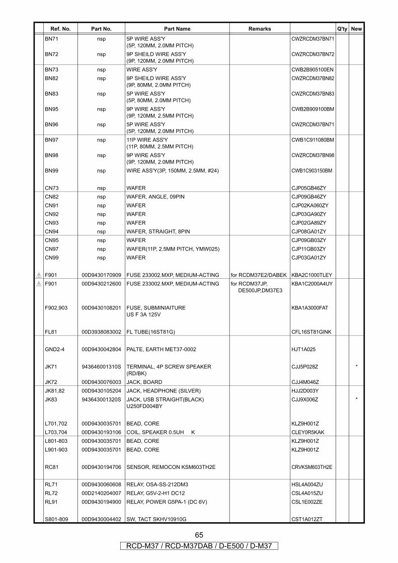
BN71 nsp 5P WIRE ASS'Y(5P, 120MM, 2.0MM PITCH)
CWZRCDM37BN71
BN72 nsp 9P SHEILD WIRE ASS'Y(9P, 120MM, 2.0MM PITCH)
CWZRCDM37BN72
BN73 nsp WIRE ASS'Y CWB2B905100ENBN82 nsp 9P SHEILD WIRE ASS'Y
(9P, 80MM, 2.0MM PITCH) CWZRCDM37BN82
BN83 nsp 5P WIRE ASS'Y (5P, 80MM, 2.0MM PITCH)
CWZRCDM37BN83
BN95 nsp 9P WIRE ASS'Y(9P, 120MM, 2.5MM PITCH)
CWB2B909100BM
BN96 nsp 5P WIRE ASS'Y(5P, 120MM, 2.0MM PITCH)
CWZRCDM37BN71
BN97 nsp 11P WIRE ASS'Y(11P, 80MM, 2.5MM PITCH)
CWB1C911080BM
BN98 nsp 9P WIRE ASS'Y (9P, 120MM, 2.0MM PITCH)
CWZRCDM37BN98
BN99 nsp WIRE ASS'Y(3P, 150MM, 2.5MM, #24) CWB1C903150BM
CN73 nsp WAFER CJP05GB46ZYCN82 nsp WAFER, ANGLE, 09PIN CJP09GB46ZYCN91 nsp WAFER CJP02KA060ZYCN92 nsp WAFER CJP03GA90ZYCN93 nsp WAFER CJP02GA89ZYCN94 nsp WAFER, STRAIGHT, 8PIN CJP08GA01ZYCN95 nsp WAFER CJP09GB03ZYCN97 nsp WAFER(11P, 2.5MM PITCH, YMW025) CJP11GB03ZYCN99 nsp WAFER CJP03GA01ZY
z F901 00D9430170909 FUSE 233002.MXP, MEDIUM-ACTING for RCDM37E2/DABEK KBA2C1000TLEYz F901 00D9430212600 FUSE 233002.MXP, MEDIUM-ACTING for RCDM37JP,
DE500JP,DM37E3KBA1C2000A4UY
F902,903 00D9430108201 FUSE, SUBMINIAITURE
US F 3A 125VKBA1A3000FAT
FL81 00D3938083002 FL TUBE(16ST81G) CFL16ST81GINK
GND2-4 00D9430042804 PALTE, EARTH MET37-0002 HJT1A025
JK71 943646001310S TERMINAL, 4P SCREW SPEAKER
(RD/BK)CJJ5P028Z *
JK72 00D9430076003 JACK, BOARD CJJ4M046ZJK81,82 00D9430105204 JACK, HEADPHONE (SILVER) HJJ2D003YJK83 943643001320S JACK, USB STRAIGHT(BLACK)
U250FD004BYCJJ9X006Z *
L701,702 00D9430035701 BEAD, CORE KLZ9H001ZL703,704 00D9430193106 COIL, SPEAKER 0.5UH K CLEY0R5KAKL801-803 00D9430035701 BEAD, CORE KLZ9H001ZL901-903 00D9430035701 BEAD, CORE KLZ9H001Z
RC81 00D9430194706 SENSOR, REMOCON KSM603TH2E CRVKSM603TH2E
RL71 00D9430060608 RELAY, OSA-SS-212DM3 HSL4A004ZURL72 00D2140204007 RELAY, G5V-2-H1 DC12 CSL4A015ZURL91 00D9430194900 RELAY, POWER G5PA-1 (DC 6V) CSL1E002ZE
S801-809 00D9430004402 SW, TACT SKHV10910G CST1A012ZT
Ref. No. Part No. Part Name Remarks Q'ty New
65RCD-M37 / RCD-M37DAB / D-E500 / D-M37
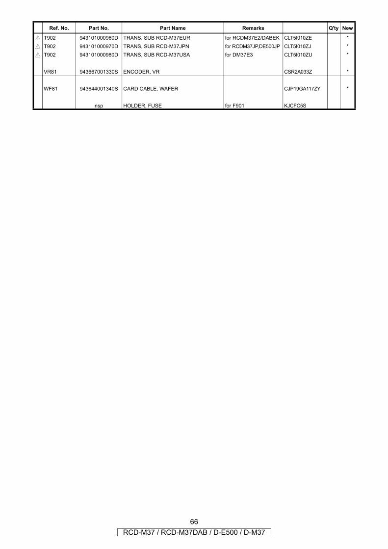
z T902 943101000960D TRANS, SUB RCD-M37EUR for RCDM37E2/DABEK CLT5I010ZE *z T902 943101000970D TRANS, SUB RCD-M37JPN for RCDM37JP,DE500JP CLT5I010ZJ *z T902 943101000980D TRANS, SUB RCD-M37USA for DM37E3 CLT5I010ZU *
VR81 943667001330S ENCODER, VR CSR2A033Z *
WF81 943644001340S CARD CABLE, WAFER CJP19GA117ZY *
nsp HOLDER, FUSE for F901 KJCFC5S
Ref. No. Part No. Part Name Remarks Q'ty New
66RCD-M37 / RCD-M37DAB / D-E500 / D-M37
--MEMO--
67RCD-M37 / RCD-M37DAB / D-E500 / D-M37

EXPLODED VIEWS
z
z
for EK model
for EK model
for JP model
for EK model
Parts marked with this symbol z have critical
characteristics.
Use ONLY replacement parts recommended by
the manufacturer.
WARNING:
z印の部分は安全を維持するために重要
な部品です。従って交換時は必ず指定の
部品を使用してください。
68RCD-M37 / RCD-M37DAB / D-E500 / D-M37
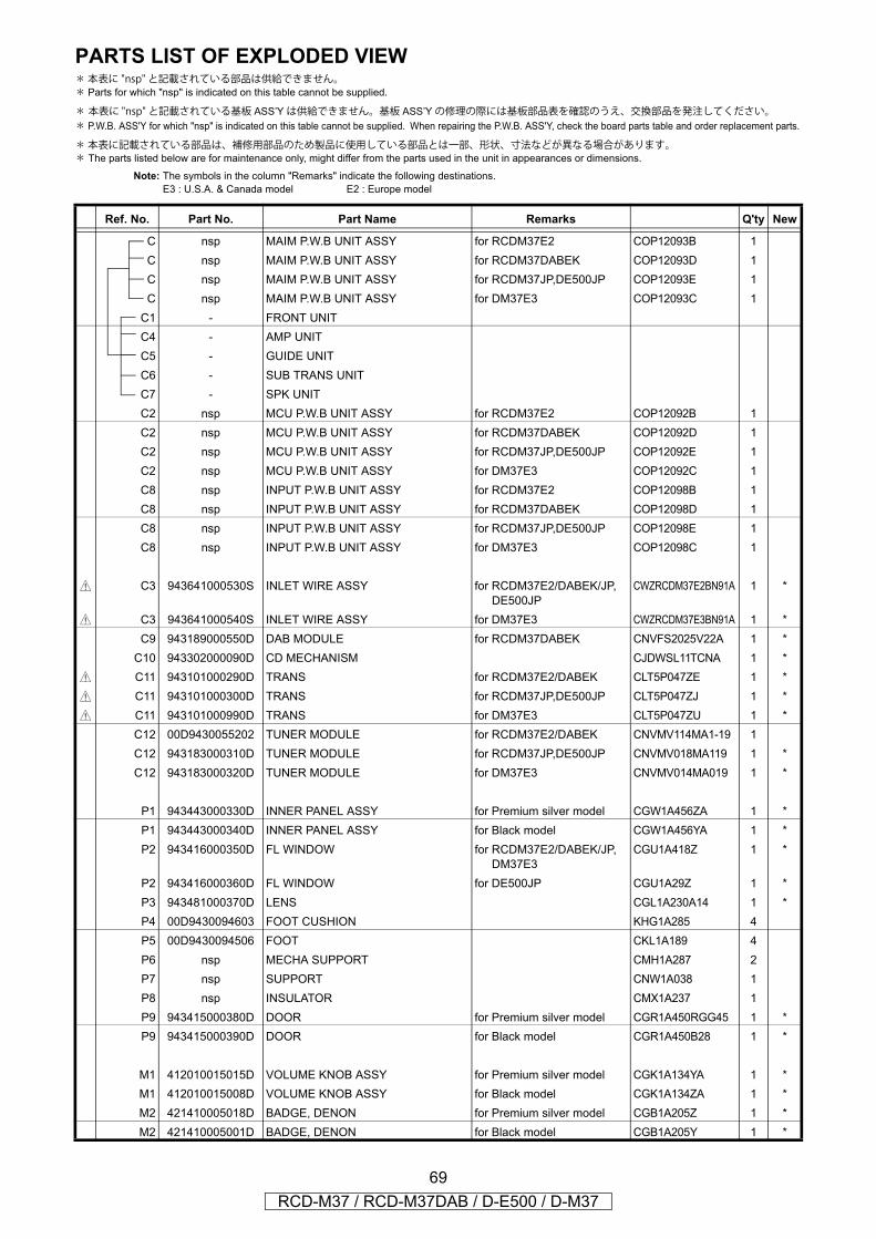
PARTS LIST OF EXPLODED VIEW* 本表に "nsp" と記載されている部品は供給できません。* Parts for which "nsp" is indicated on this table cannot be supplied.
* 本表に "nsp" と記載されている基板 ASS’Yは供給できません。基板 ASS’Yの修理の際には基板部品表を確認のうえ、交換部品を発注してください。* P.W.B. ASS'Y for which "nsp" is indicated on this table cannot be supplied. When repairing the P.W.B. ASS'Y, check the board parts table and order replacement parts.
* 本表に記載されている部品は、補修用部品のため製品に使用している部品とは一部、形状、寸法などが異なる場合があります。* The parts listed below are for maintenance only, might differ from the parts used in the unit in appearances or dimensions.
Note: The symbols in the column "Remarks" indicate the following destinations.E3 : U.S.A. & Canada model E2 : Europe model
Ref. No. Part No. Part Name Remarks Q'ty New
C nsp MAIM P.W.B UNIT ASSY for RCDM37E2 COP12093B 1C nsp MAIM P.W.B UNIT ASSY for RCDM37DABEK COP12093D 1C nsp MAIM P.W.B UNIT ASSY for RCDM37JP,DE500JP COP12093E 1C nsp MAIM P.W.B UNIT ASSY for DM37E3 COP12093C 1
C1 - FRONT UNITC4 - AMP UNITC5 - GUIDE UNITC6 - SUB TRANS UNITC7 - SPK UNITC2 nsp MCU P.W.B UNIT ASSY for RCDM37E2 COP12092B 1C2 nsp MCU P.W.B UNIT ASSY for RCDM37DABEK COP12092D 1C2 nsp MCU P.W.B UNIT ASSY for RCDM37JP,DE500JP COP12092E 1C2 nsp MCU P.W.B UNIT ASSY for DM37E3 COP12092C 1C8 nsp INPUT P.W.B UNIT ASSY for RCDM37E2 COP12098B 1C8 nsp INPUT P.W.B UNIT ASSY for RCDM37DABEK COP12098D 1C8 nsp INPUT P.W.B UNIT ASSY for RCDM37JP,DE500JP COP12098E 1C8 nsp INPUT P.W.B UNIT ASSY for DM37E3 COP12098C 1
z C3 943641000530S INLET WIRE ASSY for RCDM37E2/DABEK/JP, DE500JP
CWZRCDM37E2BN91A 1 *
z C3 943641000540S INLET WIRE ASSY for DM37E3 CWZRCDM37E3BN91A 1 *C9 943189000550D DAB MODULE for RCDM37DABEK CNVFS2025V22A 1 *
C10 943302000090D CD MECHANISM CJDWSL11TCNA 1 *z C11 943101000290D TRANS for RCDM37E2/DABEK CLT5P047ZE 1 *z C11 943101000300D TRANS for RCDM37JP,DE500JP CLT5P047ZJ 1 *z C11 943101000990D TRANS for DM37E3 CLT5P047ZU 1 *
C12 00D9430055202 TUNER MODULE for RCDM37E2/DABEK CNVMV114MA1-19 1C12 943183000310D TUNER MODULE for RCDM37JP,DE500JP CNVMV018MA119 1 *C12 943183000320D TUNER MODULE for DM37E3 CNVMV014MA019 1 *
P1 943443000330D INNER PANEL ASSY for Premium silver model CGW1A456ZA 1 *P1 943443000340D INNER PANEL ASSY for Black model CGW1A456YA 1 *P2 943416000350D FL WINDOW for RCDM37E2/DABEK/JP,
DM37E3CGU1A418Z 1 *
P2 943416000360D FL WINDOW for DE500JP CGU1A29Z 1 *P3 943481000370D LENS CGL1A230A14 1 *P4 00D9430094603 FOOT CUSHION KHG1A285 4P5 00D9430094506 FOOT CKL1A189 4P6 nsp MECHA SUPPORT CMH1A287 2P7 nsp SUPPORT CNW1A038 1P8 nsp INSULATOR CMX1A237 1P9 943415000380D DOOR for Premium silver model CGR1A450RGG45 1 *P9 943415000390D DOOR for Black model CGR1A450B28 1 *
M1 412010015015D VOLUME KNOB ASSY for Premium silver model CGK1A134YA 1 *M1 412010015008D VOLUME KNOB ASSY for Black model CGK1A134ZA 1 *M2 421410005018D BADGE, DENON for Premium silver model CGB1A205Z 1 *M2 421410005001D BADGE, DENON for Black model CGB1A205Y 1 *
69RCD-M37 / RCD-M37DAB / D-E500 / D-M37
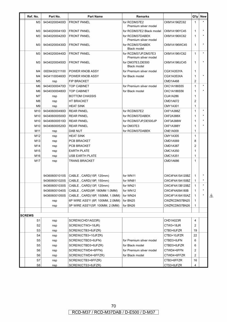
M3 943402000400D FRONT PANEL for RCDM37E2 Premium silver model
CKM1A196ZC62 1 *
M3 943402000410D FRONT PANEL for RCDM37E2 Black model CKM1A196YC45 1 *M3 943402000420D FRONT PANEL for RCDM37DABEK
Premium silver modelCKM1A196XC62 1 *
M3 943402000430D FRONT PANEL for RCDM37DABEK Black model
CKM1A196WC45 1 *
M3 943402000440D FRONT PANEL for RCDM37JP,DM37E3 Premium silver model
CKM1A196VC62 1 *
M3 943402000450D FRONT PANEL for DM37E3,DE500 Black model
CKM1A196UC45 1 *
M4 00D9430211100 POWER KNOB ASSY for Premium silver model CGX1A353YA 1M4 943411000460D POWER KNOB ASSY for Black model CGX1A353XA 1 *M5 nsp FIP BRACKET CMD1A468 2M6 943403000470D TOP CABINET for Premium silver model CKC1A186S55 1 *M6 943403000480D TOP CABINET for Black model CKC1A186S56 1 *M7 nsp BOTTOM CHASSIS CUA1A286 1M8 nsp HT BRACKET CMD1A672 2M9 nsp HEAT SINK CMY1A301 1
M10 943406000490D REAR PANEL for RCDM37E2 CKF1A388Z 1 *M10 943406000500D REAR PANEL for RCDM37DABEK CKF2A388X 1 *M10 943406000510D REAR PANEL for RCDM37JP,DE500JP CKF3A388W 1 *M10 943406000520D REAR PANEL for DM37E3 CKF1A388Y 1 *M11 nsp DAB NUT for RCDM37DABEK CNE1A009 1M12 nsp HEAT SINK CMY1A305 1M13 nsp PCB BRACKET CMD1A569 8M14 nsp PCB BRACKET CMD1A387 2M15 nsp EARTH PLATE CMC1A350 1M16 nsp USB EARTH PLATE CMC1A351 1M17 nsp TRANS BRACKET CMD1A686 1
943606001010S CABLE , CARD(15P, 120mm) for WN11 CWC4F4A15A120BZ 1 *943606001020S CABLE , CARD(19P, 150mm) for WN81 CWC4F4A19A150BZ 1 *943606001030S CABLE , CARD(13P, 120mm) for WN21 CWC4F4A13B120BZ 1 *943606001040S CABLE , CARD(9P, 180MM 1.0MM) for WN12 CWC4F4A09A180B 1 *943606001050S CABLE , CARD(16P, 150MM, 1.0MM) for WN24 CWC4F1A16A150AZ 1 *
nsp 6P WIRE ASS'Y (6P, 100MM, 2.0MM) for BN25 CWZRCDM37BN25 1nsp 5P WIRE ASS'Y(5P, 100MM, 2.0MM) for BN26 CWZRCDM37BN26 1
SCREWSS1 nsp SCREW(CHD1A023R) CHD1A023R 4S2 nsp SCREW(CTW3+18JR) CTW3+18JR 2S3 nsp SCREW(CTB3+8JFZR) CTB3+8JFZR 19S4 nsp SCREW(CTB3+10JFZR) CTB3+10JFZR 22S5 nsp SCREW(CTBD3+8JFN) for Premium silver model CTBD3+8JFN 6S5 nsp SCREW(CTBD3+8JFZR) for Black model CTBD3+8JFZR 6S6 nsp SCREW(CTWD4+6FFN) for Premium silver model CTWD4+6FFN 2S6 nsp SCREW(CTWD4+6FFZR) for Black model CTWD4+6FFZR 2S7 nsp SCREW(CTB3+6FFZR) CTB3+6FFZR 16S8 nsp SCREW(CTS3+8JFZR) CTS3+8JFZR 4
Ref. No. Part No. Part Name Remarks Q'ty New
g
70RCD-M37 / RCD-M37DAB / D-E500 / D-M37
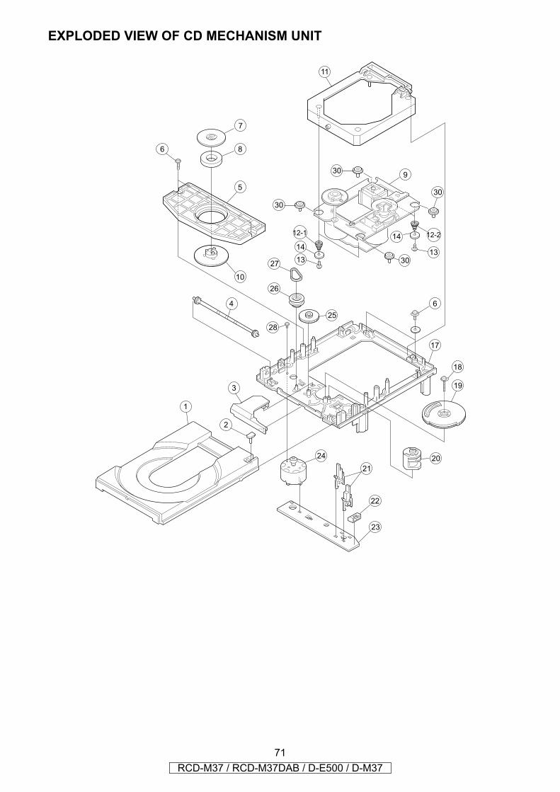
EXPLODED VIEW OF CD MECHANISM UNIT
11
13
12-214
30
30
30
6
7
8
5
10
4
1
2
3
24
21
22
23
20
19
18
17
6
25
28
26
27 13
14
12-1
30
9
71RCD-M37 / RCD-M37DAB / D-E500 / D-M37
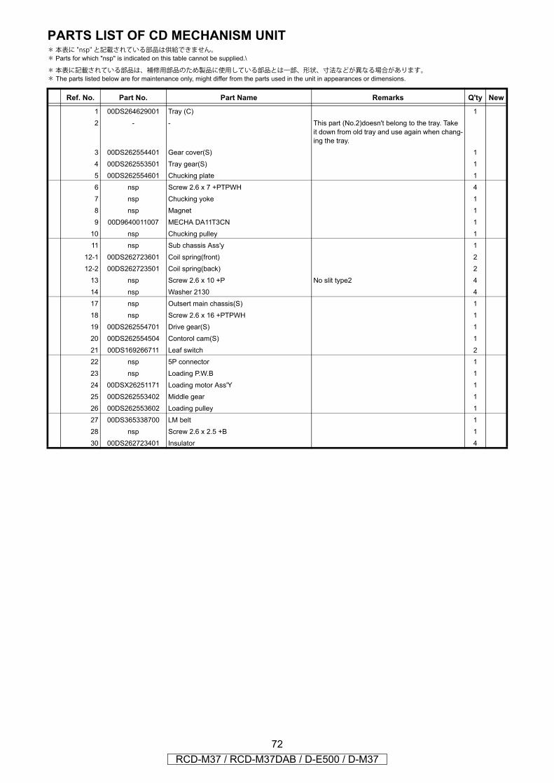
PARTS LIST OF CD MECHANISM UNIT* 本表に "nsp" と記載されている部品は供給できません。* Parts for which "nsp" is indicated on this table cannot be supplied.\
* 本表に記載されている部品は、補修用部品のため製品に使用している部品とは一部、形状、寸法などが異なる場合があります。* The parts listed below are for maintenance only, might differ from the parts used in the unit in appearances or dimensions.
Ref. No. Part No. Part Name Remarks Q'ty New
1 00DS264629001 Tray (C) 1
2 - - This part (No.2)doesn't belong to the tray. Take it down from old tray and use again when chang-ing the tray.
3 00DS262554401 Gear cover(S) 1
4 00DS262553501 Tray gear(S) 1
5 00DS262554601 Chucking plate 1
6 nsp Screw 2.6 x 7 +PTPWH 4
7 nsp Chucking yoke 1
8 nsp Magnet 1
9 00D9640011007 MECHA DA11T3CN 1
10 nsp Chucking pulley 1
11 nsp Sub chassis Ass'y 1
12-1 00DS262723601 Coil spring(front) 2
12-2 00DS262723501 Coil spring(back) 2
13 nsp Screw 2.6 x 10 +P No slit type2 4
14 nsp Washer 2130 4
17 nsp Outsert main chassis(S) 1
18 nsp Screw 2.6 x 16 +PTPWH 1
19 00DS262554701 Drive gear(S) 1
20 00DS262554504 Contorol cam(S) 1
21 00DS169266711 Leaf switch 2
22 nsp 5P connector 1
23 nsp Loading P.W.B 1
24 00DSX26251171 Loading motor Ass'Y 1
25 00DS262553402 Middle gear 1
26 00DS262553602 Loading pulley 1
27 00DS365338700 LM belt 1
28 nsp Screw 2.6 x 2.5 +B 1
30 00DS262723401 Insulator 4
72RCD-M37 / RCD-M37DAB / D-E500 / D-M37
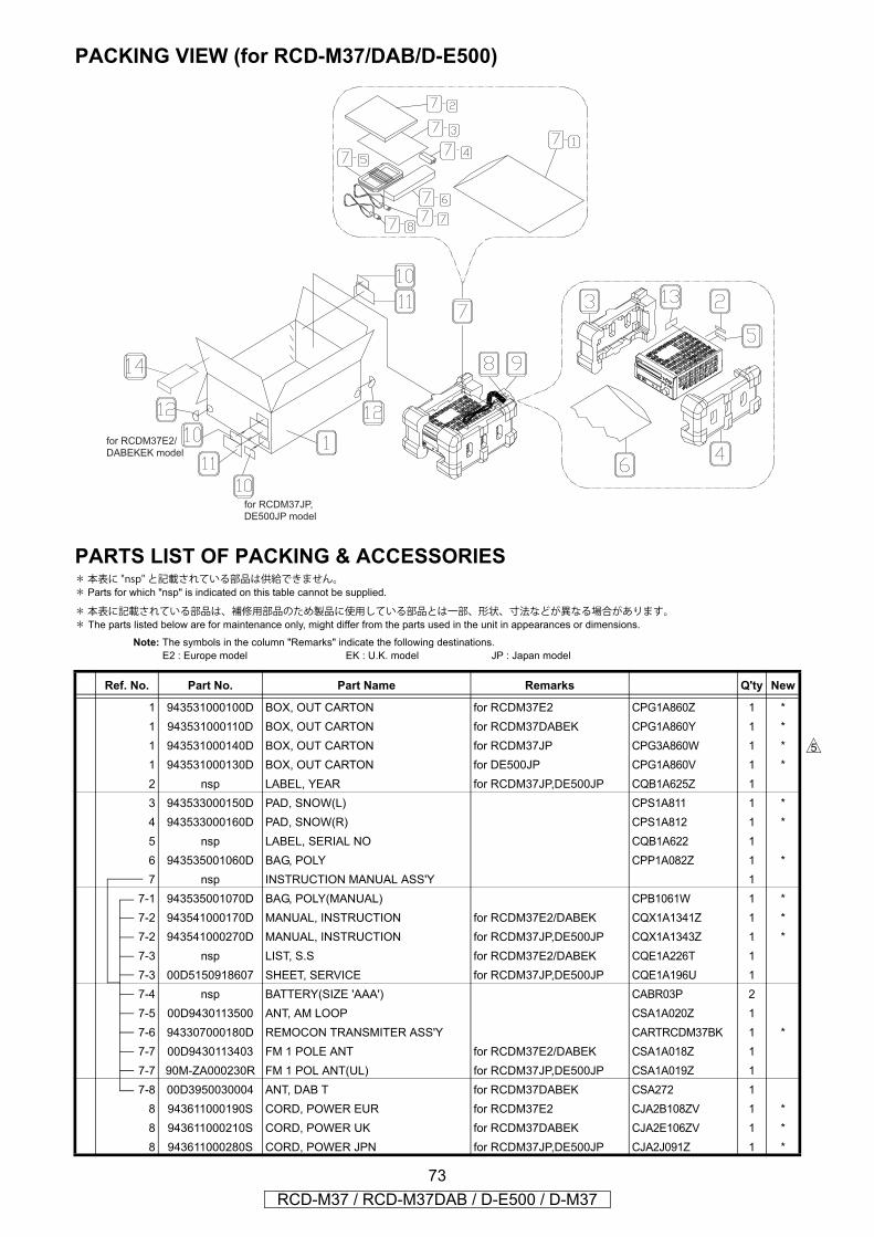
PACKING VIEW (for RCD-M37/DAB/D-E500)
PARTS LIST OF PACKING & ACCESSORIES* 本表に "nsp" と記載されている部品は供給できません。* Parts for which "nsp" is indicated on this table cannot be supplied.
* 本表に記載されている部品は、補修用部品のため製品に使用している部品とは一部、形状、寸法などが異なる場合があります。* The parts listed below are for maintenance only, might differ from the parts used in the unit in appearances or dimensions.
Note: The symbols in the column "Remarks" indicate the following destinations.E2 : Europe model EK : U.K. model JP : Japan model
Ref. No. Part No. Part Name Remarks Q'ty New
1 943531000100D BOX, OUT CARTON for RCDM37E2 CPG1A860Z 1 *1 943531000110D BOX, OUT CARTON for RCDM37DABEK CPG1A860Y 1 *1 943531000140D BOX, OUT CARTON for RCDM37JP CPG3A860W 1 *1 943531000130D BOX, OUT CARTON for DE500JP CPG1A860V 1 *2 nsp LABEL, YEAR for RCDM37JP,DE500JP CQB1A625Z 13 943533000150D PAD, SNOW(L) CPS1A811 1 *4 943533000160D PAD, SNOW(R) CPS1A812 1 *5 nsp LABEL, SERIAL NO CQB1A622 16 943535001060D BAG, POLY CPP1A082Z 1 *7 nsp INSTRUCTION MANUAL ASS'Y 1
7-1 943535001070D BAG, POLY(MANUAL) CPB1061W 1 *7-2 943541000170D MANUAL, INSTRUCTION for RCDM37E2/DABEK CQX1A1341Z 1 *7-2 943541000270D MANUAL, INSTRUCTION for RCDM37JP,DE500JP CQX1A1343Z 1 *7-3 nsp LIST, S.S for RCDM37E2/DABEK CQE1A226T 17-3 00D5150918607 SHEET, SERVICE for RCDM37JP,DE500JP CQE1A196U 17-4 nsp BATTERY(SIZE 'AAA') CABR03P 27-5 00D9430113500 ANT, AM LOOP CSA1A020Z 17-6 943307000180D REMOCON TRANSMITER ASS'Y CARTRCDM37BK 1 *7-7 00D9430113403 FM 1 POLE ANT for RCDM37E2/DABEK CSA1A018Z 17-7 90M-ZA000230R FM 1 POL ANT(UL) for RCDM37JP,DE500JP CSA1A019Z 17-8 00D3950030004 ANT, DAB T for RCDM37DABEK CSA272 1
8 943611000190S CORD, POWER EUR for RCDM37E2 CJA2B108ZV 1 *8 943611000210S CORD, POWER UK for RCDM37DABEK CJA2E106ZV 1 *8 943611000280S CORD, POWER JPN for RCDM37JP,DE500JP CJA2J091Z 1 *
for RCDM37E2/
DABEKEK model
for RCDM37JP,
DE500JP model
g
73RCD-M37 / RCD-M37DAB / D-E500 / D-M37
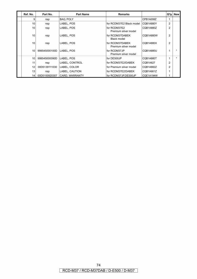
9 nsp BAG, POLY CPB1A008Z 110 nsp LABEL, POS for RCDM37E2 Black model CQB1A880Y 210 nsp LABEL, POS for RCDM37E2
Premium silver modelCQB1A880Z 2
10 nsp LABEL, POS for RCDM37DABEK Black model
CQB1A880W 2
10 nsp LABEL, POS for RCDM37DABEK Premium silver model
CQB1A880X 2
10 998545000100D LABEL, POS for RCDM37JP Premium silver model
CQB1A880U 1 *
10 998545000090D LABEL, POS for DE500JP CQB1A880T 1 *11 nsp LABEL, CONTROL for RCDM37E2/DABEK CQB1A627 212 00D5139111030 LABEL, COLOR for Premium silver model CQB1A882Z 213 nsp LABEL, CAUTION for RCDM37E2/DABEK CQB1A661Z 114 00D5150920307 CARD, WARRANTY for RCDM37JP,DE500JP CQE1A194W 1
Ref. No. Part No. Part Name Remarks Q'ty New
74RCD-M37 / RCD-M37DAB / D-E500 / D-M37
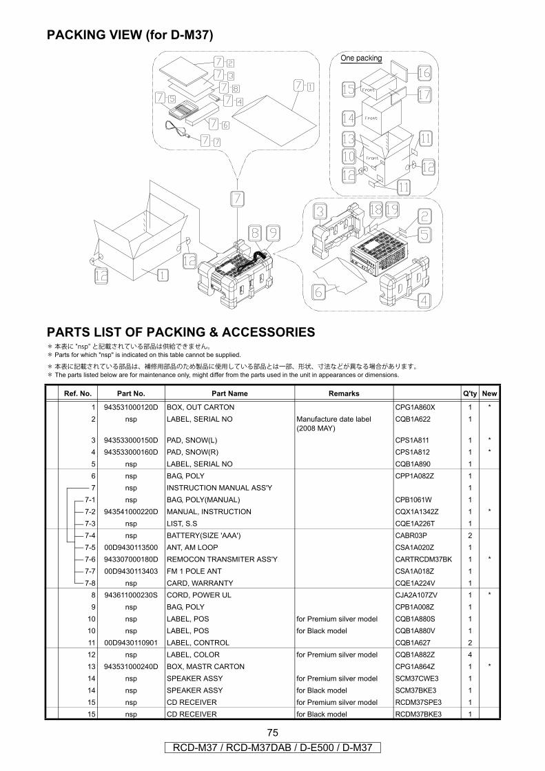
PACKING VIEW (for D-M37)
PARTS LIST OF PACKING & ACCESSORIES* 本表に "nsp" と記載されている部品は供給できません。* Parts for which "nsp" is indicated on this table cannot be supplied.
* 本表に記載されている部品は、補修用部品のため製品に使用している部品とは一部、形状、寸法などが異なる場合があります。* The parts listed below are for maintenance only, might differ from the parts used in the unit in appearances or dimensions.
Ref. No. Part No. Part Name Remarks Q'ty New
1 943531000120D BOX, OUT CARTON CPG1A860X 1 *2 nsp LABEL, SERIAL NO Manufacture date label
(2008 MAY)CQB1A622 1
3 943533000150D PAD, SNOW(L) CPS1A811 1 *4 943533000160D PAD, SNOW(R) CPS1A812 1 *5 nsp LABEL, SERIAL NO CQB1A890 16 nsp BAG, POLY CPP1A082Z 17 nsp INSTRUCTION MANUAL ASS'Y 1
7-1 nsp BAG, POLY(MANUAL) CPB1061W 17-2 943541000220D MANUAL, INSTRUCTION CQX1A1342Z 1 *7-3 nsp LIST, S.S CQE1A226T 17-4 nsp BATTERY(SIZE 'AAA') CABR03P 27-5 00D9430113500 ANT, AM LOOP CSA1A020Z 17-6 943307000180D REMOCON TRANSMITER ASS'Y CARTRCDM37BK 1 *7-7 00D9430113403 FM 1 POLE ANT CSA1A018Z 17-8 nsp CARD, WARRANTY CQE1A224V 1
8 943611000230S CORD, POWER UL CJA2A107ZV 1 *9 nsp BAG, POLY CPB1A008Z 1
10 nsp LABEL, POS for Premium silver model CQB1A880S 110 nsp LABEL, POS for Black model CQB1A880V 111 00D9430110901 LABEL, CONTROL CQB1A627 212 nsp LABEL, COLOR for Premium silver model CQB1A882Z 413 943531000240D BOX, MASTR CARTON CPG1A864Z 1 *14 nsp SPEAKER ASSY for Premium silver model SCM37CWE3 114 nsp SPEAKER ASSY for Black model SCM37BKE3 115 nsp CD RECEIVER for Premium silver model RCDM37SPE3 115 nsp CD RECEIVER for Black model RCDM37BKE3 1
75RCD-M37 / RCD-M37DAB / D-E500 / D-M37
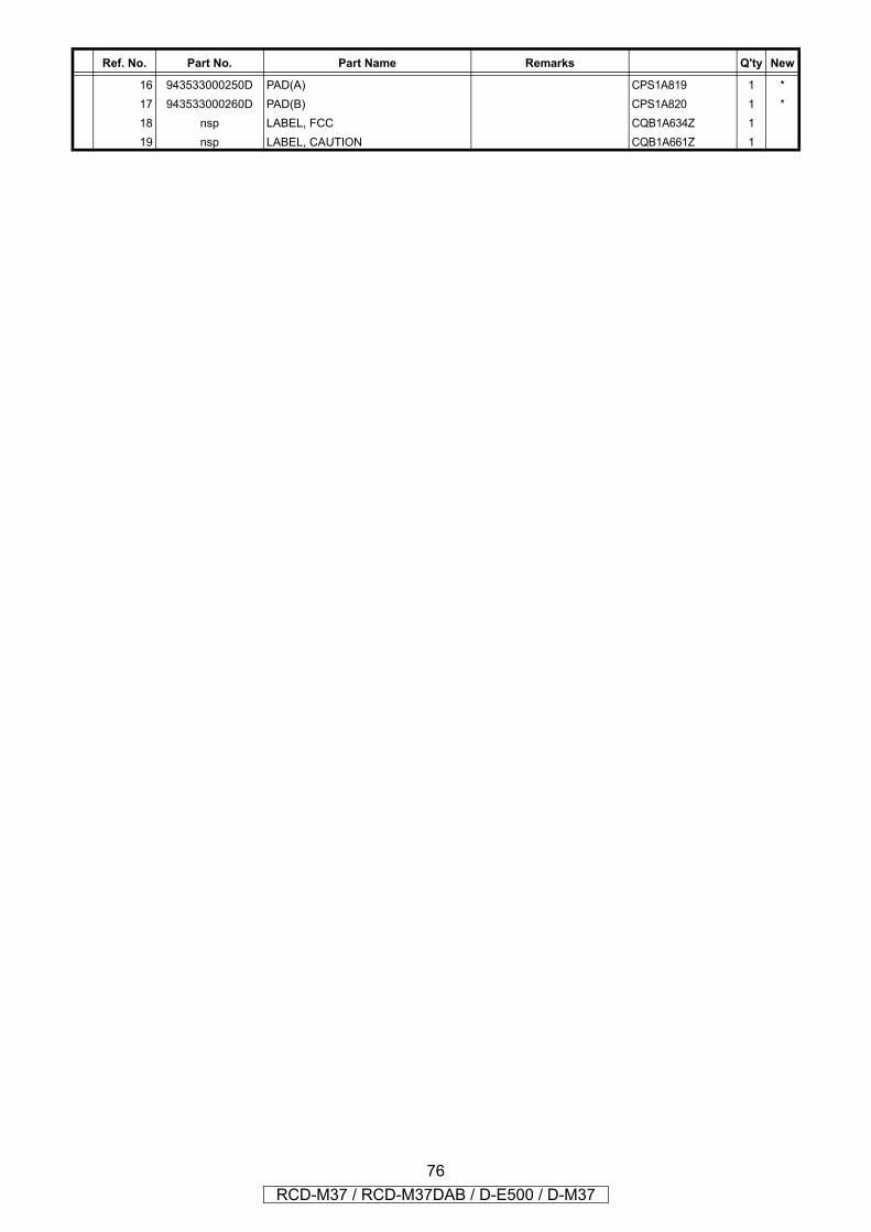
16 943533000250D PAD(A) CPS1A819 1 *17 943533000260D PAD(B) CPS1A820 1 *18 nsp LABEL, FCC CQB1A634Z 119 nsp LABEL, CAUTION CQB1A661Z 1
Ref. No. Part No. Part Name Remarks Q'ty New
76RCD-M37 / RCD-M37DAB / D-E500 / D-M37
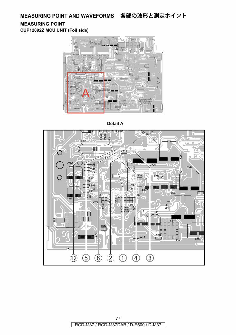
MEASURING POINT AND WAVEFORMS 各部の波形と測定ポイントMEASURING POINTCUP12092Z MCU UNIT (Foil side)
A
Detail A
erqwytQ2
77RCD-M37 / RCD-M37DAB / D-E500 / D-M37
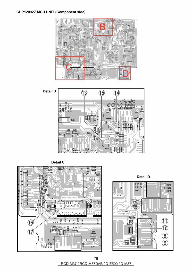
CUP12092Z MCU UNIT (Component side)
C
B
D
Q3 Q5 Q4
Q6
Q7
Q1Q0io
Detail B
Detail C
Detail D
78RCD-M37 / RCD-M37DAB / D-E500 / D-M37
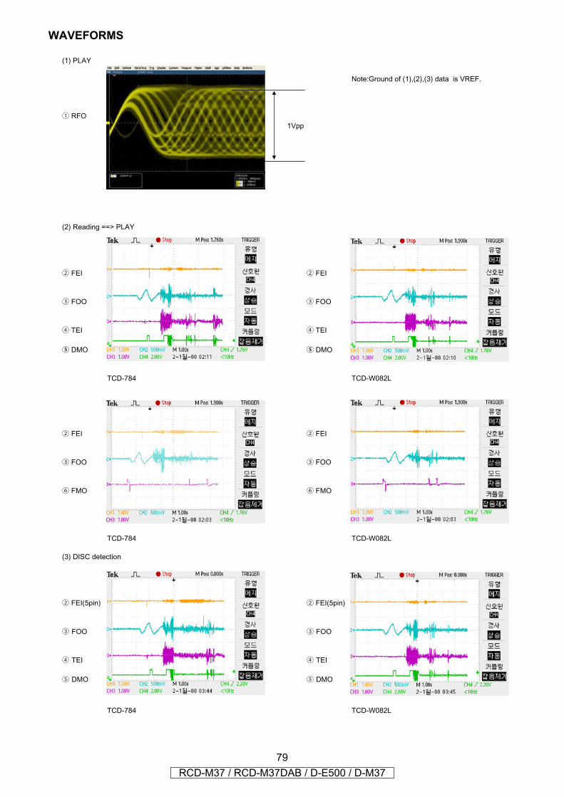
WAVEFORMS
(1) PLAY
Note:Ground of (1),(2),(3) data is VREF.
① RFO1Vpp
(2) Reading ==> PLAY
② FEI ② FEI
③ FOO ③ FOO
④ TEI ④ TEI
⑤ DMO ⑤ DMO
TCD-784 TCD-W082L
② FEI ② FEI
③ FOO ③ FOO
⑥ FMO ⑥ FMO
TCD-784 TCD-W082L
(3) DISC detection
② FEI(5pin) ② FEI(5pin)
③ FOO ③ FOO
④ TEI ④ TEI
⑤ DMO ⑤ DMO
TCD-784 TCD-W082L
79RCD-M37 / RCD-M37DAB / D-E500 / D-M37
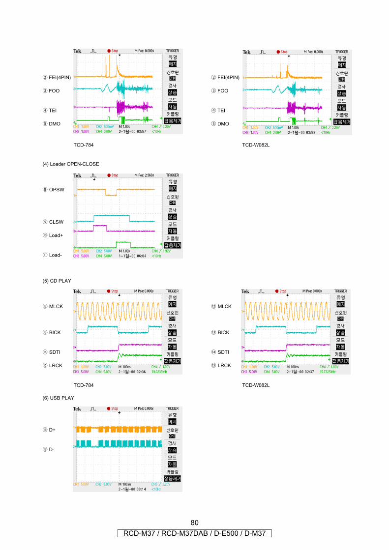
② FEI(4PIN) ② FEI(4PIN)
③ FOO ③ FOO
④ TEI ④ TEI
⑤ DMO ⑤ DMO
TCD-784 TCD-W082L
(4) Loader OPEN-CLOSE
⑧ OPSW
⑨ CLSW
⑩ Load+
⑪ Load-
(5) CD PLAY
⑫ MLCK ⑫ MLCK
⑬ BICK ⑬ BICK
⑭ SDTI ⑭ SDTI
⑮ LRCK ⑮ LRCK
TCD-784 TCD-W082L
(6) USB PLAY
⑯ D+
⑰ D-
80RCD-M37 / RCD-M37DAB / D-E500 / D-M37
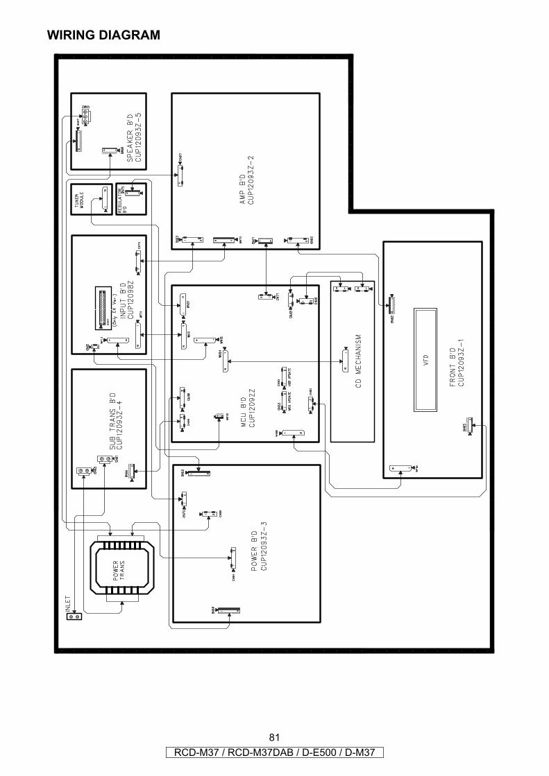
81RCD-M37 / RCD-M37DAB / D-E500 / D-M37
WIRING DIAGRAM
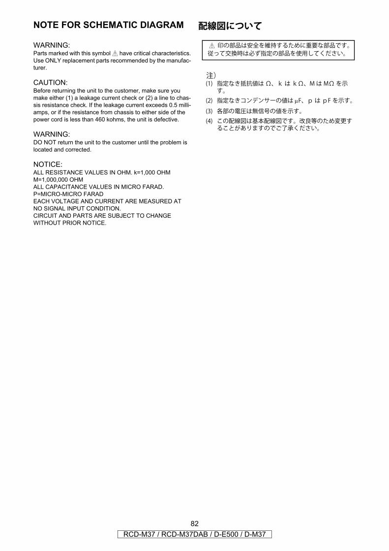
82RCD-M37 / RCD-M37DAB / D-E500 / D-M37
配線図について
z 印の部品は安全を維持するために重要な部品です。従って交換時は必ず指定の部品を使用してください。
注)(1) 指定なき抵抗値はΩ、kはkΩ、MはMΩを示す。
(2) 指定なきコンデンサーの値は μF、pはpFを示す。
(3) 各部の電圧は無信号の値を示す。
(4) この配線図は基本配線図です。改良等のため変更することがありますのでご了承ください。
NOTE FOR SCHEMATIC DIAGRAM
WARNING:Parts marked with this symbol z have critical characteristics.Use ONLY replacement parts recommended by the manufac-turer.
CAUTION:Before returning the unit to the customer, make sure you make either (1) a leakage current check or (2) a line to chas-sis resistance check. If the leakage current exceeds 0.5 milli-amps, or if the resistance from chassis to either side of the power cord is less than 460 kohms, the unit is defective.
WARNING:DO NOT return the unit to the customer until the problem is located and corrected.
NOTICE:ALL RESISTANCE VALUES IN OHM. k=1,000 OHMM=1,000,000 OHMALL CAPACITANCE VALUES IN MICRO FARAD.P=MICRO-MICRO FARADEACH VOLTAGE AND CURRENT ARE MEASURED ATNO SIGNAL INPUT CONDITION.CIRCUIT AND PARTS ARE SUBJECT TO CHANGEWITHOUT PRIOR NOTICE.
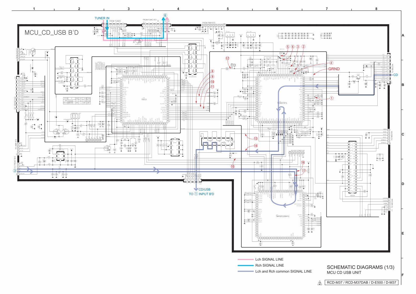
Lch SIGNAL LINE
Rch SIGNAL LINE
Lch and Rch common SIGNAL LINE
TO q INPUT B'DCD/USB
CD
e
TUNER INy
Q6
Q3
Q4
Q5
q
r
t
i
o
Q0
Q1
Q2
y e w
GRND
Q7
s
87654321
A
B
C
D
E
F
SCHEMATIC DIAGRAMS (1/3)MCU CD USB UNIT
RCD-M37 / RCD-M37DAB / D-E500 / D-M37
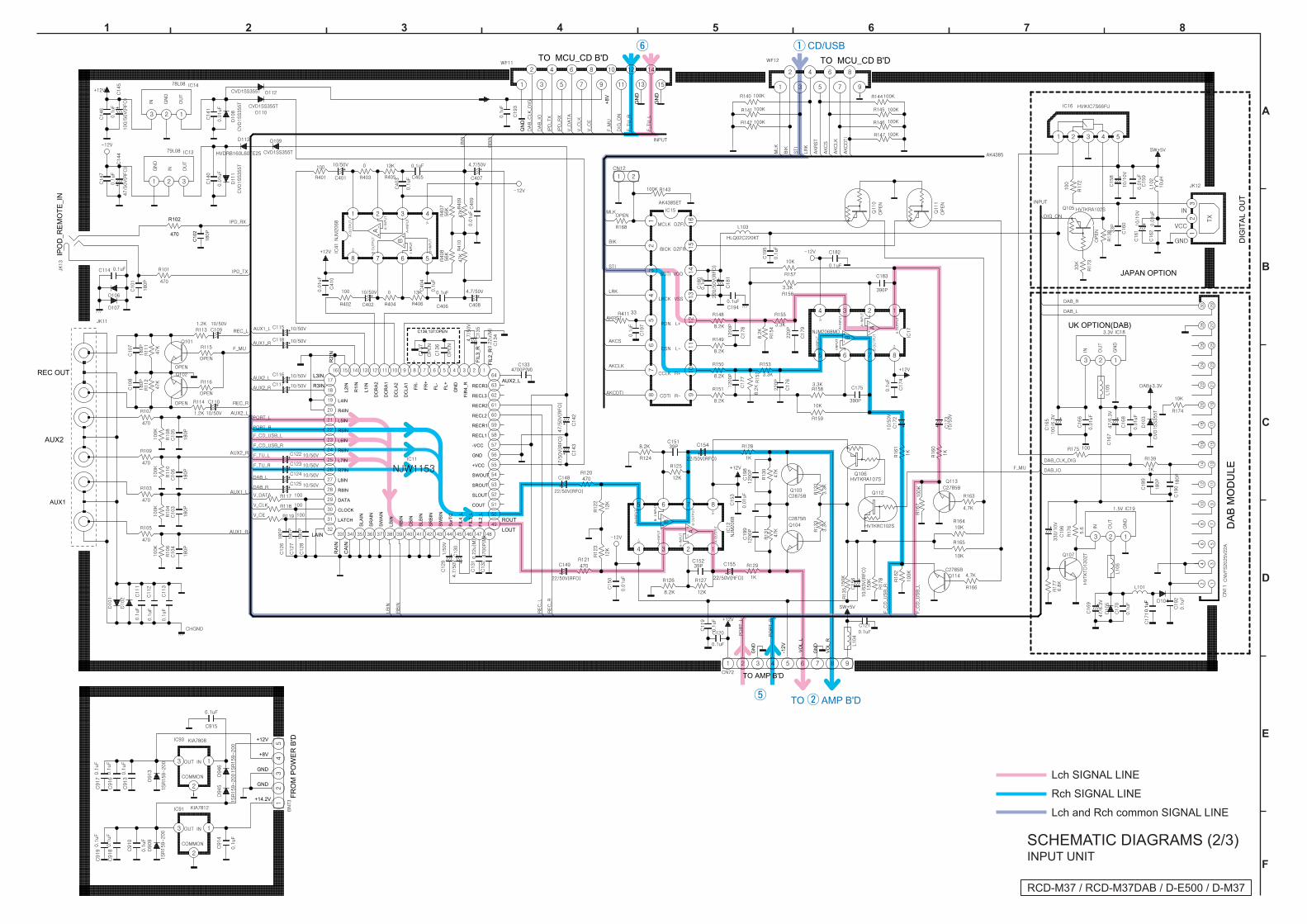
Lch SIGNAL LINE
Rch SIGNAL LINE
Lch and Rch common SIGNAL LINE
qy CD/USB
t TO w AMP B'D
87654321
A
B
C
D
E
F
SCHEMATIC DIAGRAMS (2/3)INPUT UNIT
RCD-M37 / RCD-M37DAB / D-E500 / D-M37
Lch SIGNAL LINE
Rch SIGNAL LINE
Lch and Rch common SIGNAL LINE
PORTABLE IN
e
u
r
ru
t
USB IN
H/P OUT
SP OUT
87654321
A
B
C
D
E
F
RCD-M37 / RCD-M37DAB / D-E500 / D-M37
SCHEMATIC DIAGRAMS (3/3)MAIN UNIT