delft university of technology el. instr. electronic instrumentation · 2016-02-08 · 7 et8.017...
TRANSCRIPT

1
ET8.017El. Instr.Delft University of Technology
Electronic Instrumentation
Lecturer: Kofi Makinwa
015-27 86466Room. HB13.270 EWI building
Also involved:Saleh Heidary([email protected])
ET8.017El. Instr.Delft University of Technology
Monday Sept. 24: Deterministic and Random Errors Common-mode Rejection Ratio Power supply Rejection RatioGain error
Outline

2
ET8.017El. Instr.Delft University of Technology
Deterministic Errors
where Δz denotes the uncertainty in z due to parameter a, which is specified with uncertainty Δa etc..
Assuming that the output of a system z = f(a,b,c, ...)
Then the total error due to deteministic parameter uncertainty is:
δ∂ ∂ ∂
Δ = Δ + Δ + Δ +∂ ∂
( , , ,...) ( , , ,...) ( , , ,...) ...f a b c f a b c f a b cz a b ca b c
Two kinds of errors (uncertainty):
a. Deterministic errors e.g. source loading, offset, gain error
b. Random (stochastic) errors e.g. thermal noise
The derivatives above are called sensitivities.
ET8.017El. Instr.Delft University of Technology
Additive Errors
Example: Combining additive errors:
By extension, the effect of deterministic errors (e.g. offset, gain error etc.) in a linear time-invariant (LTI) system can be determined by superposition.
For z = a + b or z = a - b with Δa the uncertainty in a and Δb the uncertainty in b, the overall uncertainty follows as:
( ) ( )a b a bz a b a ba b
∂ ± ∂ ±Δ = Δ + Δ = Δ + Δ
∂ ∂

3
ET8.017El. Instr.Delft University of Technology
Noise, interference & distortion
Interference is caused by external signals e.g. 50 Hz humNoise is caused by stochastic processes in the measurement system itself e.g. thermal noise.
Noise and interference are usually additive error signals ⇒ they can both be modeled by extra error sources to the system
Note that interference and noise should not be confused with signal distortion, which is caused non-linearities in either the amplitude or the frequency domain.
ET8.017El. Instr.Delft University of Technology
Noise + 50 Hz interference

4
ET8.017El. Instr.Delft University of Technology
Thermal noise
ALL resistors exhibit thermal noise
Thermal noise has a uniform (white) frequency spectrum
noise power density: Pn= 4kT (W/Hz)
– where k is Boltzmann’s constant and T is absolute temperature
At room temperature (293 K): Pn= 4kT = 1.62 x 10⁻²⁰ (W/Hz)
For a resistor: P = Vrms2/R = Irms
2R
=> noise voltage with spectral density: vn = √(4kTR) (V/Hz1/2)
=> noise current with spectral density: in = √(4kT/R) (A/Hz1/2)
ET8.017El. Instr.Delft University of Technology
Thermal noise (1)
v(t)
t
(Thermal) noise is stochastic, i.e. its amplitude at a given time t cannot be predicted
Thermal noise has a Gaussian amplitude distribution
2
2n2
n
1( )d d2
VVp V V e V
V π
⎛ ⎞−⎜ ⎟⎜ ⎟
⎝ ⎠=

5
ET8.017El. Instr.Delft University of Technology
Thermal noise (2)
v(t)
t
In the presence of thermal noise, the detection limit is usuallyspecified as the standard deviation (or sigma) Vn
A good estimate of its peak value (e.g. as seen on a wide-band scope) is 5-sigma
2
2n2
n
1( )d d2
VVp V V e V
V π
⎛ ⎞−⎜ ⎟⎜ ⎟
⎝ ⎠=
ET8.017El. Instr.Delft University of Technology
Shot noise
Shot noise is the result of the fact that an electrical current is the result of the motion of discrete charge carriers.This can be compared with hail on a roof: even if the average current (mass flow) is constant, the amount of charge carrriers (ice lumps), measured in different intervals with the same length Δt, will, in general, be different. The relative fluctuation becomes greater as Δt becomes smaller and smaller.Like thermal noise, shot noise has a uniform frequency spectrum and so is also a form of white noise.If a current I consists of charge carriers with charge q that move independently of each other, then the spectral noise current is given by in = √(2qI) (A/Hz1/2).This equation applies to p-n junctions (diodes, transistors, etc.) but not to metallic conductors where there is more long-range correlation between the movement of the charge carriers. In suchconductors, the shot noise will thus be smaller!

6
ET8.017El. Instr.Delft University of Technology
Calculating shot noise
in is proportional to the square-root of current!
Example (for B = 10 Hz):• I = 1 A ⇒ noise current In(rms) = 57 nA (0.000006%)• I = 1 pA ⇒ noise current In(rms) = 56 fA (5.6%)• Shot noise is important at low current levels
n 2i qI= (A/Hz1/2)
n n DC
2 1
(rms) 2with bandwidth I i B qI B
B f f= =
= −
(A)
frequency
in
f1 f2
ET8.017El. Instr.Delft University of Technology
1/f (flicker) noise
Both thermal and shot noise are the result of fundamental physical processes and so form a fundamental detection limit.
Apart from these types of noise, “real” electronic components also suffer from several sources of “excess noise.”
Resistors exhibit current-dependent 1/f noise: Vn(rms) = c⋅Iwhere the constant c is determined by resistor quality (price).
Transistors (especially MOSFETs) exhibit area-dependent 1/f noise:where Vn(rms) ∝ 1/sqrt(Area) 1/f noise has a 1/f POWER spectrum, i.e. the spectral noise power per decade (or per octave) is constant.
1/f noise is sometimes referred to as “pink” or “flicker” noise

7
ET8.017El. Instr.Delft University of Technology
3 instances of 1/f ruis
Peak amplitude increases for as measurement time increases?!
x ~ t
More and more important for long (low-frequency) measurements!
1/f noise example
ET8.017El. Instr.Delft University of Technology
Spectrum of a critically damped micro-mechanical structure
Two spectral regimes: a. 1/f noise andb. frequency independent white noise.
Real noise spectrum

8
ET8.017El. Instr.Delft University of Technology
On-line noise demo
http://socrates.berkeley.edu/~phylabs/bsc/Supplementary/NoiseGenerator.html
ET8.017El. Instr.Delft University of Technology
Non-electrical noise
Noise is also present in non-electrical domainsThermal noise ⇒ some kind of energy dissipation
In the mechanical domain this is due to dampingIn very small structures (MEMS), Brownian noise is also importantIn the thermal domain this is due to thermal resistance
Shot noise ⇒ small amount of energy-carrying particlesIn the optical domain, photon shot noise is significant

9
ET8.017El. Instr.Delft University of Technology
Error propagation
where σz2 denotes the variance (uncertainty) in parameter z with
average value z due to parameter a, which is specified with uncertainty σa etc..
The effect of stochastic error(s) on overall system specifications can be evaluated using Gauss law of error propagation:
Errors (uncertainties) due to:a. Noise,b. Electro-Magnetic Interference (EMI)
are referred to as Stochastic (random) sources of error (uncertainty).
2 2 22 2 2 2
, , ,... , , ,... , , ,...
( , , ,...)
( , , ,...) ( , , ,...) ( , , ,...) ...σ σ σ σ
=
∂ ∂ ∂⎛ ⎞ ⎛ ⎞ ⎛ ⎞= ⋅ + ⋅ + ⋅ +⎜ ⎟ ⎜ ⎟ ⎜ ⎟∂ ∂ ∂⎝ ⎠ ⎝ ⎠ ⎝ ⎠z a b c
a b c a b c a b c
z f a b c
f a b c f a b c f a b ca b c
ET8.017El. Instr.Delft University of Technology
Error propagation and equivalent input error
Combining additive errors:
In case of distributed noise voltages or currents:
Hence, the variances of stochastic errors in a linear system can be linearly added.
For z= a+ b or z= a-b the overall uncertainty follows as:
( ) ( )2 22 2 2 2 2
, , ,... , , ,...
σ σ σ σ σ
= ±
∂ ± ∂ ±⎛ ⎞ ⎛ ⎞= ⋅ + ⋅ = +⎜ ⎟ ⎜ ⎟∂ ∂⎝ ⎠ ⎝ ⎠
z a b a b
a b c a b c
z a b
a b a ba b

10
ET8.017El. Instr.Delft University of Technology
Error propagation and equivalent input error
Combining additive errors:
In case of distributed noise voltages or currents:
Hence, the variances of stochastic errors in a linear system can be linearly added.
For z= a+ b or z= a-b, the overall uncertainty follows as:
( ) ( )2 22 2 2 2 2
, , ,... , , ,...
σ σ σ σ σ
= ±
∂ ± ∂ ±⎛ ⎞ ⎛ ⎞= ⋅ + ⋅ = +⎜ ⎟ ⎜ ⎟∂ ∂⎝ ⎠ ⎝ ⎠
z a b a b
a b c a b c
z a b
a b a ba b
2 2, 1 2= +n eq n nu u u
2 2, 1 2= +n eq n ni i i
Provided these are independent !
ET8.017El. Instr.Delft University of Technology
Error propagation and equivalent input error
Noise paradox:
Adding the thermal noise powers of R1 and R2 to the noise power due to in flowing through R1 and In flowing through R2:
What is the equivalent noise voltage in a circuit with two resistors connected to a noise current source ?
( )
( )
2 2 2 2 2 2 21, , 1 , 2 1 2
2 2 2 2 2, 1 , 2 1 2
n eq n R n R n n
n R n R n
a u = u +u +i R +i R =
u +u +i R + R

11
ET8.017El. Instr.Delft University of Technology
Error propagation and equivalent input error
Noise paradox:
Adding the thermal noise powers of R1 and R2 to the noise power due to in flowing through R1 and In flowing through R2:
What is the equivalent noise voltage in a circuit with two resistors connected to a noise current source ?
( )
( )
2 2 2 2 2 2 21, , 1 , 2 1 2
2 2 2 2 2, 1 , 2 1 2
n eq n R n R n n
n R n R n
a u = u +u +i R +i R =
u +u +i R + R
( ) ( )2 2 2 22, , 1 , 2 1 2
2n eq n R n R nb u = u +u +i R + R
Adding the thermal noise powers of R1 and R2 to the noise power due to in flowing through R1 plus R2:
X
V
ET8.017El. Instr.Delft University of Technology
Equivalent input sources
General approach for finding equivalent input noise sources:

12
ET8.017El. Instr.Delft University of Technology
Note: equivalent noise is independent of source impedance!
Extreme case 1:open input.
Hence:
Equivalent input sources
General approach for finding equivalent input noise sources:
2 2 2 22 1 1 2 22 22 , 1
2 22 2
( ) ( )
( )
⎫= + +⎪
= ⎬⎪= ⎭
a n i n o n
b n eq i
a b
u i R A i R u
u i R A
u u
2 2 22 2 2 2, 1 2 2
1
+= + n n o
n eq ni
u i Ri iA R
ET8.017El. Instr.Delft University of Technology
Note: equivalent noise is independent of source impedance!
Extreme case 2:short-circuited input.
Hence:
Equivalent input sources
General approach for finding equivalent input noise sources:
2 2 2 22 1 1 2 22 22 , 1
2 22 2
( ) ( )
( )
⎫= + +⎪
= ⎬⎪= ⎭
a n n o n
b n eq
a b
u u A i R u
u u A
u u
2 2 22 2 2 2, 1 2
1
+= + n n o
n eq nu i Ru u
A

13
ET8.017El. Instr.Delft University of Technology
Recommendations for low-noise performance:Focus design effort on first stage: low noise and high gain, A1.
Equivalent input sources
2 2 22 2 2 2, 1 2 2
1
+= + n n o
n eq ni
u i Ri iA R
2 2 22 2 2 2, 1 2
1
+= + n n o
n eq nu i Ru u
A
General approach for finding equivalent input noise sources:
ET8.017El. Instr.Delft University of Technology
Noise in components is usually specified in terms of the noise spectral power, sn. In case of a resistor:
Noise bandwidth
2,
2,
[ /Hz]V
[ /Hz]A
nu Z B B
B Bni Z
s = 4k T Z 4k TR 4k T 4k Ts =
Z R
=
=
Noise bandwidth is the bandwidth of a theoretical low-pass filter with an abrupt cut-off frequency at B. A practical low-pass filter will have a more gradual transition from pass-band to stop-band, H(ω).
frequency
vn
0 B
At 20°C and into a 10kHz bandwidth, a 10kΩ resistor generates 1.3 µVrms.

14
ET8.017El. Instr.Delft University of Technology
Noise bandwidth
is defined as the bandwidth of a “brick wall” filter with an abrupt cut-off frequency at B. A practical system is specified by a low-pass filter with a more gradual transition from pass-band to stop-band, H(ω).
The Noise bandwidth B of a practical low-pass filter can be obtained from its transfer function, H(ω) as follows:
( ) ( )21ω ω ω ω
∞ ∞
→ =∫ ∫2 22
n o0 0o
P = H B = H d B H dH
ET8.017El. Instr.Delft University of Technology
Noise bandwidth of a first-order system
( ) ( )21ω ω ω ω
∞ ∞
→ =∫ ∫2 22
n o0 0o
P = H B = H d B H dH
( )( ) [ ]
0
/c20
1dB = = arctg = = rad s ,2 21+π πω ωτ ωτ τωτ
∞∞
∫
For noise calculations, a “correction factor” π/2 is required
For Ho=1:

15
ET8.017El. Instr.Delft University of Technology
Noise in impedance, Z, is primarily due to the dissipating (resistive) part, R:
Noise in passive components
2,
2,
[ /Hz]V
[ /Hz]A
nu Z B B
B Bni Z
s = 4k T Z 4k TR 4k T 4k Ts =
Z R
=
=
Reactive components are not free of noise due to parasitics:
( )( )
2 2 2 2 2 2 22 41
2ω πω ωπω
π∞ ∞
=+
∫ ∫2 B
nC n n p n pB
pp p p0 0 p
d 4k Tu = i Z d = i R i R = R =R C 2 R 2R CC
kR
TC
ET8.017El. Instr.Delft University of Technology
Noise in passive componentsReactive components are not free of noise due to parasitics:
( )( )
2 2 2 2 2 2 22 41
2ω πω ωπω
π∞ ∞
=+
∫ ∫2 B
nC n n p n pB
pp p p0 0 p
d 4k Tu = i Z d = i R i R = R =R C 2 R 2R CC
kR
TC
In a capacitor:
Similarly, in an inductor:
( ) ( )2 2
22
ω ωωωω ωπ
∞ ∞ ∞
×⎛ ⎞⎜ ⎟⎝ ⎠
∫ ∫ ∫2
n B snL n2 2 2
s0 0 0s
s
B4k TR 1d dui = d = u = =RR + LZ L1+
R
k T2 L

16
ET8.017El. Instr.Delft University of Technology
Ex. Calculation equivalent input noise sources
Ideal current source, thus in,eq only (open-input)
Trans-impedance amplifier:
Hence,2 2 2 2 2 2 2 21 1 1 2 ,o n n f nR o n eq fu = u +i R +u = u = i R
2 22 21, 12 2
n nRn eq n
f f
u ui = +i +R R
Uo/Ii= (-)Rf
For:sni,1= 1 pA/sqrtHz,Rf=10 kΩ and4kBT= 1.65 10-20 J @300 K
,
,
. . .
.
− −−⎛ ⎞
⎜ ⎟⎝ ⎠
29 202 24 2-24n eq 44
2n eq
4.10 1 65 10i = + + = 2 8.10 [A /Hz]10 1010
i = 1 67 pA/ Hz
ET8.017El. Instr.Delft University of Technology
SNR is defined as the ratio between signal power and noise powerexpressed in dB:
2
S
N
(rms)10 log(rms)
VV
⎛ ⎞= ⎜ ⎟
⎝ ⎠S
N
(rms)20 log(rms)
VV
⎛ ⎞= ⎜ ⎟
⎝ ⎠S
N
S 10 logN
PP
⎛ ⎞= ⎜ ⎟
⎝ ⎠Notes:
Since the form of the signal and that of the noise may differ significantly, SNR should not be calculated from signal amplitudes but from rms values.A given SNR is always associated with a certain bandwidth.For maximum SNR, the bandwidth of a measurement system should be about the same as the expected signal bandwidth
Signal-to-noise ratio (SNR)

17
ET8.017El. Instr.Delft University of Technology
Noise matching
Best noise performance implies that readout adds no noise to thenoise power already included in the source.
How can we optimize the NF of a practical system?
The noise added by the readout is specified in the Noise factor, F:
( )( )( )
( ) ( )
( ) ( )( )
( )( )
ω +⎡ ⎤⎣ ⎦
input
output
s
n n n n
s n n2
n
SNRF = =
SNR
P inputP source P source + P readout P readout
= = 1+P output P source P source
H P source readout
ET8.017El. Instr.Delft University of Technology
Noise matching
Noise matching in a practical system:
( )( )
input n
output n
SNR P readoutNF = = 1+
SNR P source
2 2 2n n g
B g
u +i R= 1+
4k TR
Minimum at: ( )( )
2 2 22 2
2
B g n g B n n g
2g B g
2 ng,opt
n
4k TR 2i R - 4k T u +i RNF = = 0 R 4k T
u=RiR
×∂→
∂
Resulting in a minimum noise factor:2
minn
B g
2uNF = 1+4k TR
Minimum NF indicates best redistribution of noise over un,eq and in,eqat the minimum noise power, Pn(readout), derived before.

18
ET8.017El. Instr.Delft University of Technology
Noise matching
Noise matching using a series resistance?
- Noise matching at higher noise level.- Attenuation of Ug
Noise matching using series resistance is counter productive
( ) ( )2 2 →2
n B g B s n n g ssource+ readout = 4k TR +4k TR +u +i R + RP
( ) ( ) ( )2 2 2 22 2
B g s n n n ng s g ss
B g g B g
4k T R + R +u +i u iR + R R + RRNF = = 1+4k TR R 4k TR
++
ET8.017El. Instr.Delft University of Technology
Analog to Digital Conversion
Signal is quantized in both amplitude and in time
v(t)
t

19
ET8.017El. Instr.Delft University of Technology
• Range: 0 - Vref
• Number of bits: n
• Number of levels: 2n
• “step-size”: q = Vref.2-n
• error: -½q < V < ½q
• For a busy signal (one that jumps between many quantization levels), this error can be modeled as random noise with a uniform pdf
• The associated standard deviation e is then given by:
22
2
1 112
q
q
e V dV qq −
= =∫
V
Probability distr. function p(V)
½q-½q
1/q
Quantization Noise
ET8.017El. Instr.Delft University of Technology
Sources of interference
integrated circuitconductionelectrostatic discharge
audio systemmagnetic fieldtransformer (50 Hz)
high-impedance sensorelectric fieldSwitched-mode PSU
FM radioelectromagnetic fieldHF digital circuit
Interference sensitive system
Coupling mechanism
Interference source

20
ET8.017El. Instr.Delft University of Technology
Interference via conduction
Coupling via a common impedanceE.g. via a common supply line or a ground connection
i1
time
Circuit 1 : HF digital circuit⇒ i1 is a rapidly varying current (high di/dt )
VsCircuit 2Circuit 1
i1
VR L
ΔV = R i1 + L di1/dt
VVs
ET8.017El. Instr.Delft University of Technology
Common impedances: solutions
Quick fix: use a bypass capacitor near a HF circuit to locally deliver its rapidly changing supply currents (this can be seen as a form of filtering)Good design: avoid shared impedances
C
Local charge storage
di/dt
Seperate supply lines

21
ET8.017El. Instr.Delft University of Technology
External sources of error
Ground loops
Additive error due to IaRa in series with ug.
ET8.017El. Instr.Delft University of Technology
External sources of error
Ground loops
“star” connection to limit error due to IaRa.

22
ET8.017El. Instr.Delft University of Technology
Electric & magnetic coupling
Electric (capacitive) coupling is due to changing voltages, i.e. dV/dtMagnetic (inductive) coupling is due to changing currents, i.e. dI/dt
sensitivecircuit
source of interference
1
2
1
2
In the same circuit there can be multiple coupling mechanisms– Depends on source and load-impedances, size and geometry
electric fielddV/dt
Capacitance b/w two conductors
magnetic fielddI/dt
Shared magnetic flux between two loops
ET8.017El. Instr.Delft University of Technology
Electromagnetic interference
When an “antenna” is driven by a source, it creates– an electromagnetic field– an electric field– a magnetic field
In a given situation, the dominant field depends on the shape and size of the antenna, the frequency and the distance to the antennaField strengths vary with:
– 1/R2 and 1/R3 voor electric and magnetic fields, resp.1/R for EM-waves (R = distance to antenna)
– R < λ: E and M fields can dominate (near field)– R > λ: EM waves can dominate (far field)
The following applies to EM waves:– L = λ/2: good antenna (lots of EM interference)– L < λ/20: bad antenna (less problems)
R
Lstoringsbron
23
ET8.017El. Instr.Delft University of Technology
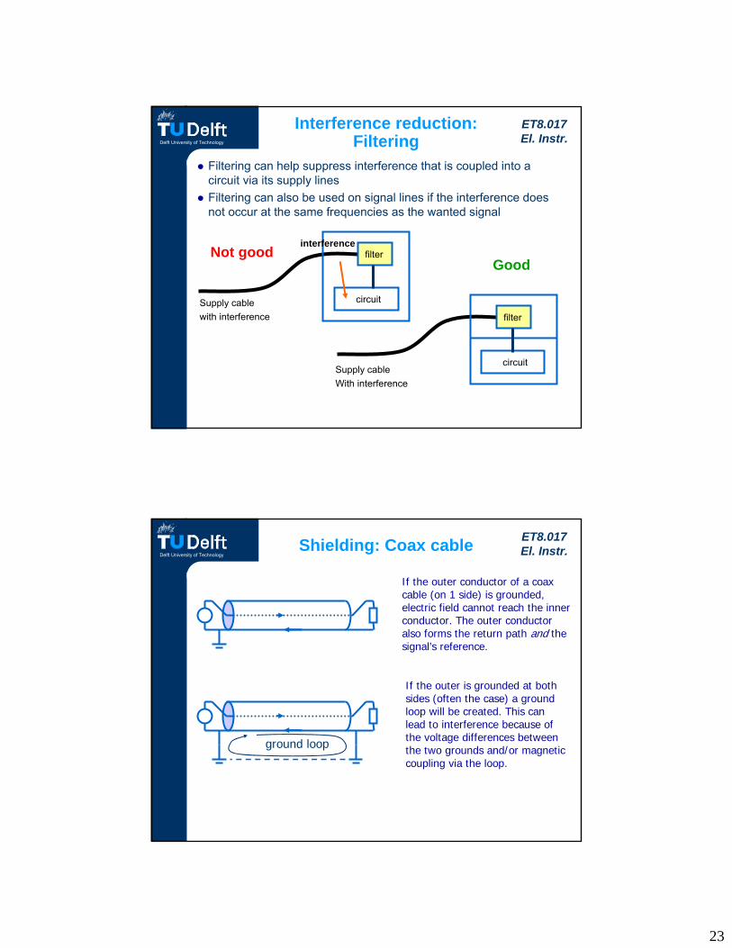
Interference reduction: Filtering
Filtering can help suppress interference that is coupled into a circuit via its supply linesFiltering can also be used on signal lines if the interference does not occur at the same frequencies as the wanted signal
filter
circuit
Not goodinterference
Supply cable with interference
Supply cableWith interference
filter
circuit
Good
ET8.017El. Instr.Delft University of Technology
Shielding: Coax cable
If the outer conductor of a coax cable (on 1 side) is grounded, electric field cannot reach the inner conductor. The outer conductor also forms the return path and the signal’s reference.
If the outer is grounded at both sides (often the case) a ground loop will be created. This can lead to interference because of the voltage differences between the two grounds and/or magnetic coupling via the loop.
ground loop

24
ET8.017El. Instr.Delft University of Technology
Twisted pair
signal current
induced current
M
• Magnetic field induces current in coils
• coils are “twisted”• currents in neighboring
loops have opposite signs• currents cancel each other• net induced current is zero
untwisted pair (ref)twisted pairuntwisted pair + alu foil shielduntwisted pair + steel shield
50 Hz Magnetic shielding
Attn [ dB ]043332
ET8.017El. Instr.Delft University of Technology
Twisted pair (2)
+V
• An electrical field• Couples capacitively to both conductors• Generates equal currents in both signal and return lines• Signal line: current flows through Rs//RL generates +V• Return line: current flows to ground (low R)
• Result: electric fields are not shielded!• Solutions:
• Add capacitive shielding (e.g. a conducting outer layer) • Balance the circuit
ERs
RL

25
ET8.017El. Instr.Delft University of Technology
Twisted pairs: Balancing
+
-
Balancing:• Use differential inputs and outputs• Ensure that capacitively coupled currents in both lines are the
same (i.e. that they are common-mode signals) and that they “see” the same impedance
• The current-induced voltages will then cancel each other out• Adding an outer shield will then result in excellent suppression of
both magnetic and electric interference
Icm +V
+V
(+V) - (+V) = 0
ET8.017El. Instr.Delft University of Technology
Shielding: EM waves• EM waves will not penetrate a closed conducting enclosure if it is at
least 10 “skin depths” thick• The enclosure does not need to be grounded• EM waves can leak into the enclosure via:
• Cables that enter the enclosure • Use filters and/or shield the cables
• Openings in the enclosure such as:• plastic knobs• displays• Ventilation holes• Poorly designed connectors
box1 box2cables
Completely closed system
f...1
μσπδ =
δ = skin depthσ = conductivityμ = permeabilityf = frequency
1δ = 8.7 dB attn.(= 2.7 x)

26
ET8.017El. Instr.Delft University of Technology
Types of cable
untwisted pair
coaxial
twin-axial
twisted-pair
twisted-pairshielded
Most types of cable can be obtained with an extra outer shield for even better suppression of EM interference
ET8.017El. Instr.Delft University of Technology
Shielding
Shielding to reduce capacitive coupling
,
//1//
ω
=+
i
i
gi n n
gc
Z Zu u
Z Zj C
, =+
i
ii g g
g
Zu uZ Z
Non-shielded interconnect:
Applying an electrically conductive shield:
( ),
,
,
/
/
//
/
//
/
↓↓
→ ↓
→
=+
i
i i
i n nc
i ai g g
g a
a
i g g
u u
B
CZ Zu u
Z Z Z
Z Z
W u u
Z

27
ET8.017El. Instr.Delft University of Technology
Active guarding (1)
Active guarding reduces capacitive coupling, and maintains BW
Applying an electrically conductive shield:
Active guarding:
No current flowing through Za. Hence: Z’a=Ui/Ia >> Za
ET8.017El. Instr.Delft University of Technology
Active guarding (2)
Active guarding reduces capacitive coupling, and maintains BW
Applying an electrically conductive shield:
Active guarding:Ia= ui-(1-ε)ui]/Za. Hence: Z’a= Ui/Ia = uiZa/εui= Za/ε
Stability: ε positive !

28
ET8.017El. Instr.Delft University of Technology
Suppressing electric fieldsKnowing how electric (capacitive) coupling arises, it is “easy” to avoid this type of interference:
Reduce the signal impedancesThe coupling cap and the signal impedance form a voltage divider
Drop the frequency and amplitude of the interfering signalUsually not possible
Decrease the coupling capacitanceIncrease the distance between interference and circuitGround floating conductors between interference and circuit
Break any return path for interferenceThese usually form ground loops
Capacitive shielding:Shielded cables (e.g. coax)Conducting box around sensitive circuitsGround the shielding!
ET8.017El. Instr.Delft University of Technology
Assignment 3a
A voltage-to-current converter with trans-conductance Gm= 1 A/V is used to readout a sensor with source resistance Rs= 4 kΩ.The voltage-to-current converter consists of a transconductor with gm= 10 mA/V followed by a current amplifier with Gi= 100The transconductor’s equivalent noise voltage and current are:un = 1 nV/√Hz and in = 0.5 pA/√Hz. Its input resistance is 100kΩ.The current amplifier’s equivalent noise voltage and current are:un = 100 nV/√Hz and in = 10 pA/√Hz. Its input resistance is 10Ω.Calculate the converter’s equivalent noise voltage and current
gm Gi
Rs
Vs
virtual ground of next stage
Iout

29
ET8.017El. Instr.Delft University of Technology
Assignment 3b
Calculate the detection limit due to noise of the readout, if the bandwidth of interest lies between 20Hz and 20kHz.The source also produces both 1/f and thermal noise. Assuming that the latter is due to the 4k resistor and that the 1/f corner frequency is 1kHz, calculate the new detection limit
Rs
Vs
virtual ground of next stage
gm Gi
ET8.017El. Instr.Delft University of Technology
Assignment 3b
The circuit is mounted close to a power cable and so suffers from capacitively-coupled 50Hz interference.Calculate the input-referred voltage if Ck1 = Ck2 = Ck3 =1pFWhat can be done to reduce the power-line coupling?
Rs
Vs
virtual ground of next stage
220V/50Hz
Ck1 Ck2 Ck3
gm Gi