defect detectability in eb-welded copper disposal canister with 9 … · 2008-12-07 · defect...
TRANSCRIPT

Developments in Radiographic Inspection Methods
Defect Detectability in EB-welded Copper Disposal Canister with 9 MeV Accelerator J. Pitkänen, T. Salonen, Posiva Oy, Finland; S. Sandlin, VTT, Finland; U. Ronneteg, Bodycote, Sweden
ABSTRACT
In Finland the disposal canister structure consists of a nodular graphite cast iron insert covered by a 50
mm thick copper over pack. The canister has three versions, one for each reactor type in Finland. The fuel
is sealed into the canisters in whole fuel assemblies including the possible flow channel outside the
bundle. The capacity of the canister is 12 assemblies of BWR or VVER 440 fuel and 4 assemblies of EPR
fuel. The canister shall be tight with a high probability for at least 100 000 years. The good and long
lasting tightness requires:
• Good initial tightness that is achieved by high quality requirements and extensive
• Quality control,
• Good corrosion resistance (over pack of micro-alloyed oxygen-free copper) and
• Mechanical strength of the canister that is ensured by analyses;
Following loads are considered: hydrostatic ground water pressure, even and uneven swelling
pressure of bentonite, thermal effects, and elevated hydrostatic pressure during glaciations. The canister
shall limit the radiation dose rate outside the canister to minimize the radiolysis of the water in the
vicinity of the canister. Moreover, the canister insert shall keep the fuel assemblies in a sub-critical
configuration even if the void in the canister is filled with water due to postulated leakage.
In this construction the copper lid will be welded to copper over pack with electron beam welding
(EBW). In EB-welding the kinetic energy converts to heat, when focused beam of high-accelerated
electrons hits the target material copper. This high voltage (150kV) EBW-equipment uses high vacuum,
with power of 50 kW. In the EB-weld several defect types can occur like:
• Internal root defect
• Void or cavities caused by spiking
• Gas porosity
• Excess of penetration
• Cavities
• Defects caused gun discharge
One specific reference specimen shown in the figure 1 was welded in high vacuum EBW-
equipment with keyhole technique for the radiography study on the detectability of these defect types.
The specimen was cut in pieces along the middle of the weld and artificial defects simulating above
mentioned defect types were inserted in the weld and specimen was built up reassembled again. For the
radiographic inspection a 9 MeV Linac was used to inspect this specimen and detectability of each
simulated defect types will be shown in this study.
ELECTRON BEAM WELDING
In electron beam-welding gases will be emitted during melting that causes more requirements to carry out
welding properly /1/. Emitting gases cause porosity. For precaution deoxidizers must be used in
preventing the weld porosity. Welding process will be controlled over a very wide range of parameters.
The electron beam is tightly focused and the total heat input is much lower than that of any arc welding
process. As a result, the effect of welding on the surrounding material is minimal, and the heat-affected
zone is narrow. Possible distortion is slight and the work piece cools rapidly. In electron beam welding,
joining of metal is produced with the heat generated by bombarding it with a high-velocity electron beam.
For more papers of this publication click: www.ndt.net/search/docs.php3?MainSource=70
6th International Conference on NDE in Relation to Structural Integrity for Nuclear and Pressurized ComponentsOctober 2007, Budapest, Hungary

At a typical accelerating voltage used for welding of 150 kV electrons reach a speed of 2 x10⁸ m/s. Speed
is equivalent to two-thirds the speed of light. Electrons impinge the surfaces to be joined and nearly all of
their kinetic energy is transformed into heat. In Figure 1 on left is shown the principles of EB-welding
equipment, where the electron beam will be controlled and directed with help of changing magnetic field
produced by annular winding. Heat vaporizes the base metal and allows the electron beam to penetrate
until the specified depth is achieved. Electron beam produces a keyhole in the material, which is filled as
the beam passes by. In Figure 1 on right are shown the phases of the keyhole formation.
Electron Beam
Magnetic
field lines
Annular
winding
Focal
distance
Electron beam Electron beam
Vapour Key hole Vapour
Electron beam
Key holeVapour
EBW
Electron beam
Figure 1 – Principle of electron beam steering in EBW-equipment and keyhole formation in EB-Welding
In electron beam welding, the complete joint penetration is called keyhole-welding technique/1, 2,
3/, shown in Figure 1 on the right. In the majority of the electron beam welding applications, this
technique is employed to accomplish complete joint penetration in a single weld pass, clarified in Figure
2 /4/. As liquid-walled keyhole moves along the centerline of the butt joint, liquid metal in the weld pool
flows from the front to the back of the advancing keyhole. Solidifying weld pool in electron beam
welding produces a fusion weld that is narrow, parallel sided and completely penetrated /5/.
Figure 2 – Principle of electron beam welding of thick specimen with keyhole technique

DEFECT TYPES IN ELECTRON BEAM WELDING
As the base metal melts and solidifies during the welding process, several undesirable phenomena may
occur which cause defects in the weld /1, 4, 6, 7/. Welding of the copper canister is performed with the
partial joint penetration technique. The keyhole does not completely pass the copper shell due to the
design aspects. The root of the weld forms into the copper shell.
Internal Root Defects
Weld profile in electron beam welding of thick copper is normally deep and narrow. This may cause the
vapor pressure during welding to be insufficient to hold the melt in a stable uniform shape. Unstable melt
slides forwards, collapses and falls near the bottom of the keyhole. The collapsing melt can block a part of
the keyhole. The partly blocked keyhole bottom solidifies rapidly and can cause a cold shut.
In normal conditions, the weld root has a constantly altering profile. With the high penetration
values the electron beam is focused very narrow at the root and the profile can vary greatly. If the welding
parameters are incorrect, the spiking effect can cause the deep and narrow needles to be filled
insufficiently by the molten material,
Cavities, precisely cold shuts and spiking defects, are formed in the root. Cavities can usually be
avoided or minimized by reducing the welding speed, broadening the weld and increasing the radius of
the weld root.
Gas Porosity
Gas pores are formed in the melt either as a result of metallurgical gaseous reactions or during cooling as
a result of the decreasing solubility of gases. Because of the rapid solidification of the melt, formed gases
cannot escape quickly enough. Gas porosity is usually in the form of small pores, up to 0.5 mm diameter,
even though full weld width pores are possible. The welding speed has the greatest effect on the porosity
in copper whereas impurities present in Cu-OFP copper have hardly any effect on porosity.
Excess of Penetration
Excess of penetration is not a real defect for acceptance of the copper canister. But after formation of
excess of penetration the inspection volume changes in a way that can cause lack of inspection and
defects can be formed in the volume, which is not in inspection area, and it generates possibility non-
detection of defects for NDT. In that sense the penetration depth have to be hold in predefined limits.
Cavities
Cavities formed during the welding are generally larger than gas pores. They form during solidification as
a result of solidification shrinkage and in the direction of solidification towards the centerline. Cavities
are typically 3-4 mm in diameter and they may extend for long distances at the root of the weld or in the
run-out region. The size makes them more serious than the pores.

Gun Discharge Defects
Possible discharges in the electron gun are some of the most important problems of electron beam
welding. Discharge is not directly a defect, but it can cause severe damage to the weld, if it happens. Gun
discharge can happen, if metal vapor or impurity elements enter the electron gun during the process. As a
result of the electrical discharge, the control voltage collapses and the beam current increases until a
current limiting relay cuts it. This leads to defects in the weld. If the electron beam is suddenly
interrupted, it generally leaves behind an end crater. Discharges that do not lead to welding being stopped
can result in a crack- like defect that arises from shrinkage and can extend to the full depth of the weld.
Defects resulting from severe gun discharge can usually be repaired subsequently with difficulty.
Development has been made to prevent gun discharging. Increasing the working distance can do it and
using advanced electrical control systems, which prevent an extreme increase in the current, by
controlling the power supply functions, very rapidly. Another possibility is to deflect or bend the electron
beam in the electron gun. With tilting of the beam, it is possible to ensure that the molten particles ejected
from the point of impingement of the beam cannot enter the electron gun.
Run Out
In the keyhole welding technique, the residual energy of the electron beam keeps the keyhole open on the
underside of the work piece and affects the shape of the root cap of the weld. If an excessively high beam
current is set for a particular welding operation, the surface tension developed during melting may not be
sufficient to support the too large fusion envelope and weld pool against the force of gravity. Molten
metal can flow downwards, causing concavity in the crown and droplets of the metal along the root or
falling from the root. If the beam current is set too low, it will not completely melt the full thickness of
the work pieces to be joined and will result in an excessively convex weld crown.
Welding Stresses
Heating and cooling during the welding process builds up stresses in the welded structure. The residual
stresses are those, which remain in the welded structure after cooling to room temperature. All stresses in
the welded structure can cause formation of different types of cracking. In copper welding the crack
formation has not been detected yet. For nearly planar defect types, see Figure 3, NDT of thick copper
weld residual stresses forms interesting challenge in case of compression.
Figure 3 - Root spiking defect in copper EB-weld /4/.

Figure 4 –Sketches of different defect types in the EB-weld
SIMULATED EB-WELD DEFECTS
In order to test radiographic detection capability following reference defects were designed and
manufactured with EDM:
• Volumetric defects in square and cylindrical form simulating gas porosity cavities and foreign
material like wolfram,
• Volumetric defects in J-Form and U-form simulating small cold lap that can be detected easily with
ultrasonic but more difficult to detect with radiography,
• Surface Notches on the surface which simulate crack type of defects and run out defect types,
• Long EDM drill holes (50 mm long) simulating Gun discharge defects,
• Defects made in Oval form simulating spiking and root defect type
Figure 5 - Reference copper specimen layout for EB-weld X-ray study
The reference specimen (70° from whole circumference) in length of 450 mm was cut out from real
size copper weld. The outer diameter of the specimen was 1050 mm. Before cutting the EB-weld of the
specimen was inspected with ultrasonic testing and radiography. The result from X-ray inspection is
shown in Figure 6.

Figure 6 - X-ray inspection results of the whole circumference (3300 mm) of the EB-welded to reference
specimen before manufacturing defects
The part of the weld, where no defects were found, was chosen for reference specimen. Reference
specimen was manufactured from 4 copper weld pieces. The central part of specimen was cut along the
middle of the weld with ED-wire tapping machine. The cutting result is shown in Figure 7. The cut
surface was visually inspected and 5 small defects were found, which 3 of them were in normal inspection
area in the root of the weld and 2 clearly outside of inspection volume, areas where penetration was
higher than 50 mm, which should be the normal penetration. The largest defect was about 3 mm in size
and the other about 2 mm in size. They were not detected in the radiography but 2 small root indications
were detected in ultrasonic inspection.
Figure 7 - Weld was ED wire-tapping machined in the middle of the weld. Specimen shown after wire
machining

RADIOGRAPHIC EQUIPMENT
The main principle is that the canister rotates, while the accelerator generates X-rays through the systems
for digital radiography is supplied by BIR (Bio-Imagine Research Inc.), see Figure 8. The main
components are:
• Varian’s 9 MeV linear accelerator
• Manipulator for positioning of accelerator and detector.
• Detector system consisting of a collimated vertical line-camera.
• Computer system for setting up the inspection and evaluation of results.
Weld with specific angle of incidence is shown in Figure 9 on left. The line camera (detector)
collects the transmitted X-rays and an X-ray image with 0.4 mm resolution is generated see Figure 9 on
the right.
Figure 8 - X-ray systems used for inspection of the seal weld at the Canister Laboratory in SKB.
Figure 9 - Sketch of X-ray inspections for Finnish EB-weld (on the left) and X-ray image showing surface
defect indications in the weld (on the right)

A collimator placed at the front of the accelerator focus of the beam and the detector is placed into a
housing of tungsten to reduce the scatter. The X-rays passes through the 70 mm housing in a 0.4 mm wide
vertical slit. As the penetrated thickness varies in the X-ray inspection of the weld, a thickness correction
is made to calibrate the system, Figure 9. The correction is made by a mean value calibration from 500
samples around the weld circumference. It can be seen in the radiography images of Figure 9 on the right
that the software doesn’t correct perfectly the thickness variations. In Figure 10 is shown the thickness
variation, which is seen by the detector with exposure angle of 10° and 20°. The penetrated wall thickness
is with an angle of 10° about 20 mm less than with angle of 20° in root area. Mainly of this reason the
angle 10° has been chosen for this weld inspection. For instance in case of FSW the weld is welded from
the side of the canister and the used angle of exposure is about 30°. In Figures 11 and 12 are shown
arrangement for reference specimen measurements.
0
20
40
60
80
100
120
0 10 20 30 40 50 60 70 80 90
Detector position [mm]
Th
ickn
ess [
mm
]
Exposure angle 20
Exposure angle 10
Figure 10 - Wall thickness is a function of angle between X-ray source and specimen. Wall thickness
variations are shown with exposure angles of 10° and 20°
Figure 11 - Arrangement for X-ray measurements with the reference specimen and the detector

Detek
tor
EB
-Weld
Soru
ce
Surface
Root Sou
rce
Detecto
r
Figure 12 - Test set up for Radiographic measurements with reference specimen
EVALUATION OF MEASUREMENTS
In Figure 13 is seen almost all reference defects. The detection capability is shown in Figures 14, 15, 16
and 17. All 49 artificial defects in manufactured reference specimen were detected in radiography
inspection. The chosen defects for Figure 14 are pointed out in blue square in Figure 13. The gray value
of defect having smallest volume with dimension 1x1x1mm3
is pointed out with red circle. In the Figure
17 is shown the intended thickness of those defects. As it can be seen on Figure 17 that thickness varies
little bit over the whole length of defects because of difficulties in manufacturing of these long defects.
The smallest thin long defect was detected clearly almost over the whole its length.
Figure 13 - Results from radiographic measurements with exposure angle of 10°. Defect in round form
having dimensions of 1x1x1mm3 is pointed out with red circle.
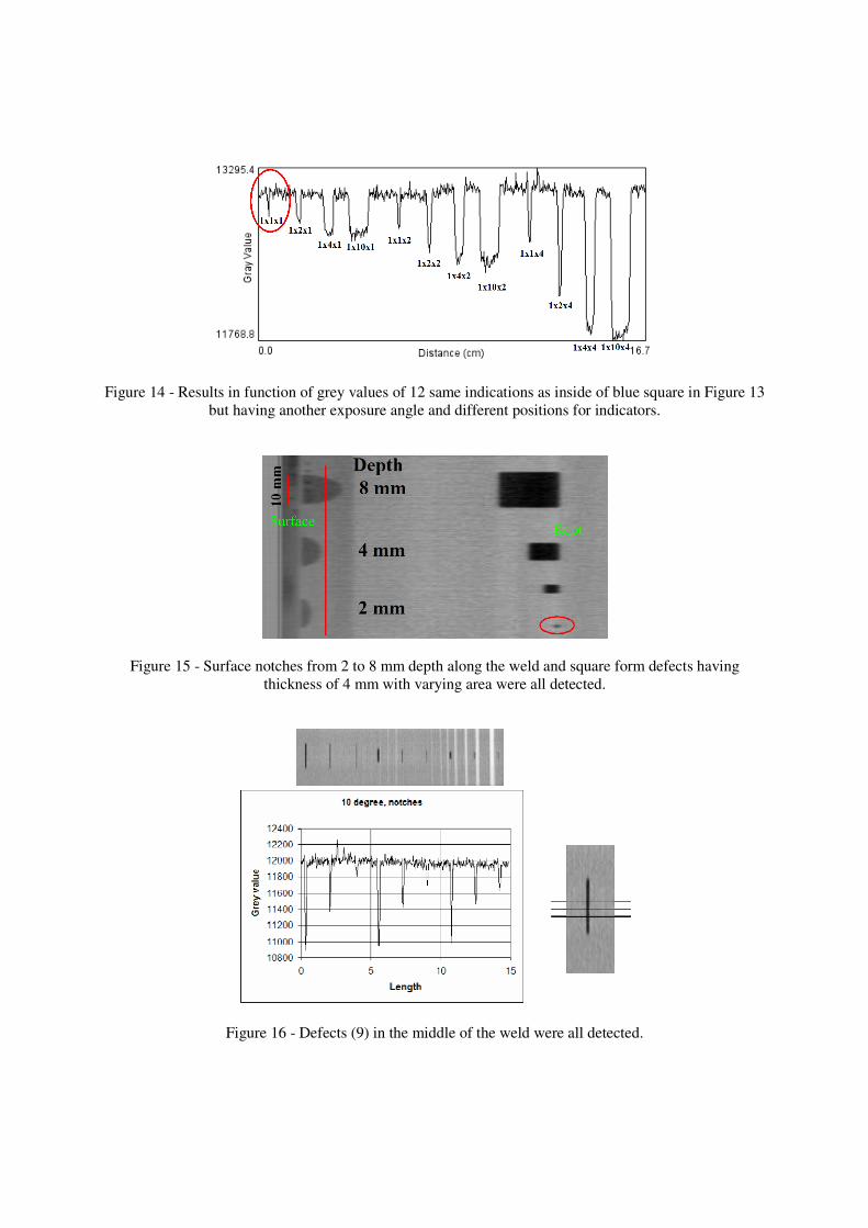
Figure 14 - Results in function of grey values of 12 same indications as inside of blue square in Figure 13
but having another exposure angle and different positions for indicators.
Figure 15 - Surface notches from 2 to 8 mm depth along the weld and square form defects having
thickness of 4 mm with varying area were all detected.
Figure 16 - Defects (9) in the middle of the weld were all detected.

0.5 mm
1.0 mm
1.5 mm
2,0 mm
50,0 mm
Figure 17 - Simulated gun discharge defect types were all detected.
DETERMINATION OF IMAGE QUALITY FROM THE MEASURED GRAY VALUES OF THE
REFERENCE SPECIMEN
Some examples of image quality values determined according to the standard EN13068-1 are given /8/.
The image quality values given here correspond to an IQI placed in the X-ray path going through the root
of the EB-weld. A duplex wire IQI was used to determine basic un-sharpness while wire and hole type
IQIs are used to measure image contrast /8/. The detection criterion for wires and holes is based on
Equation 1/8/. A wire or hole is regarded as detected if the signal to noise ratio (SNR) is larger than 2. A
SNR analysis is performed for the weakest peaks. The analysis of the X-ray images was done using
software called ImageJ. Minimum image quality values for wire and step-hole IQIs are given in Annex B
of EN 1435 /9/ for different penetrated thicknesses. Further, the maximum allowed duplex wire un-
sharpness values and maximum pixel size when using X-rays with energy over 1 MeV are given in
reference /10/. The following analysis corresponds to the beam angle 10 degrees. Image quality values
measured using step-hole IQI are not presented here as these IQI:s are not recommended for use in digital
radiography. Further, note that the image quality values given by hole type IQI:s are sensitive to the
angle at which the X-ray deviates from being parallel to the axis of the cylindrical holes (especially for
small diameter holes).
Image Quality Value Using a Wire Type IQI in the Root Area of the EB-weld
An EN 462 W6 Cu 50 image quality identifier was placed in the X-ray path passing through the root of
the weld /11, 12/. The gray value profile plot is shown in Fig. 18. As can be seen wires W6, W7, and W8
are detected above the noise level /8/. The SNR for wire W8 is 2.68 and 1.75 for the hardly distinguished
wire W9. The IQI was placed on the both detector and source side (profile plots not shown for the source
side). The image quality value (number of the thinnest visible wire) is therefore W8 in this case.

EN 462 W6, 10 degrees, right, file 5007
13700
13750
13800
13850
13900
13950
14000
14050
0 50 100 150
Distance, pixels
Gre
y v
alu
e
Figure 18 - IQI value estimated to be W8 in case of X-ray passing the root of EB-weld
Basic Un-sharpness using Duplex Wire Measurements
The duplex wire IQI was placed on the detector side in the X-ray path passing through the root of the EB-
weld. In the gray level profile plots the wire pairs are seen as twin peaks. The wire pairs are considered to
be resolved if the dip between the twin peaks is at least 20% of the maximum /10/. In practice the twin
peaks may have different heights (not mentioned in the standard); in such cases the height of the lower
peak is taken as the maximum. The maximum is measured from the mean noise level to the maximum of
the mentioned peak. Further, we need to determine which of the twin peaks are distinguished from the
noise level (i.e. SNR > 2). The weaker of the twin peaks is used also for this purpose.
From Fig. 19 it can be concluded that the peaks from wire pairs 1D, 2D, 3D and 4D are all clearly
detected. The wire pair 4D is also resolved as the dip is 34.7% of the maximum. Therefore the first
unresolved wire pair is 5D. The wire diameter (d) and wire spacing (also d) of these wires is 0.320 mm;
the corresponding un-sharpness is therefore 2d = 0.64 mm /13/.
The profile in Fig. 20 is plotted for comparison with the duplex wire IQI on the source side. No
further analysis is needed, it is clearly seen that wire pairs 1D, 2D, 3D and 4D are resolved and detected
and that the first unresolved wire pair is 5D. Note that the separation between the peaks as larger in this
case as compared to the previous case where the IQI was on the detector side. This is due to a larger
projection magnification because the IQI is further away from the detector.
Duplex wire, 60 mm, 10 degrees, file 5003
13000
13100
13200
13300
13400
13500
13600
0 50 100 150
Distance, pixels
Gre
y v
alu
e
Figure 19 - The first unresolved wire pair is 5D X-ray passing trough the root of the EB-weld.

Duplex wire, 10 degrees, source side, file 5008
13700
13800
13900
14000
14100
14200
14300
0 50 100 150
Distance, pixels
Gre
y v
alu
e
Figure 20 - Gray values plotted for comparison with the duplex wire IQI on the source side showing first
unresolved wire pair to be 5D.
Image Quality Values Using the Hole IQI or ASME Penetrameter
This IQI was also placed in the X-ray path passing through the root of the EB-weld. This IQI was used
only on the detector side. In this case the plotted grey scale profiles are such that the detectability of the
holes can be determined directly from the profiles without SNR analysis. From Fig. 21 it can be
concluded that all three holes are detected /14/.
Hole IQI at 60 mm, 10 degrees, file 5008
13700
13750
13800
13850
13900
13950
14000
14050
14100
14150
0 20 40 60 80
Distance, pixels
Gre
y v
alu
e
Figure 21 - The hole IQI placed in the X-ray path passing through the root of the EB-weld. All three
holes are detected.
Comparability of Image Quality to Standards
According to standard /15/ the wire IQI value (class A) should be at least 7 in the thickness range above
55 to 85 mm and at least 6 in the thickness range above 85 to 150 mm. As can be seen from Table 1 the
IQI values measured on both the detector side and on the source side are 8, so we conclude that the
demands of standard EN 462-3 are fulfilled /15/.
For acceleration voltages higher than 1 MV the standard EN 14784-2 /10/ requires that the first
unresolved wire pair should be 6D or higher, in this work the first unresolved wire pair is 5D, see Figures

19 and 20. The requirements in this standard in therefore not fulfilled even if we are very close. However,
using digital detectors, a limited spatial resolution can be compensated for by a higher signal to noise ratio
(SNR).
Table 2 summarizes the results for the hole IQI or ASME penetrameter. In this case all three holes
were observed.
Table 1 - Detected wires in the EN 462 W6 Cu 50 image quality indicator with the IQI placed in the X-
ray path passing through the root of the EB-weld, see Fig. 18.
EN 462 W6 Cu 50 IQI position
at the root of the weld
Wire Detector side Source side
W6 yes yes
W7 yes yes
W8 yes yes
W9 no no
W10 no no
W11 no no
W12 no no
Table 2 - Detected holes using the hole IQI or ASME penetrameter image quality indicator, see Fig. 21.
The thickness T of the penetrameter is 1.02 mm (0.04 inch).
Hole IQI position at the root of the weld
1T yes
2T yes
4T yes
SUMMARY AND CONCLUSIONS
For nuclear fuel disposal the use of copper canisters has been introduced in Finland. For sealing of these
canisters EB-welding has been studied. To ascertain the quality the canister welds will be inspected with
radiography and ultrasonic testing for volumetric defects. In this study we concentrated on defect detect
ability in radiographic inspection.
A reference specimen has been manufactured containing different types of defects - totally 49
artificial defects. These artificial defect types have been chosen to simulate defect types in electron beam
welding of thick copper. The weld dimensions of the specimen (diameter 1050 mm) were same as in the
real size canisters but the tube length was only about 400 mm. The wall thickness of the copper tube was
50 mm. The weld was inspected before defect manufacturing using mechanised ultrasonic inspection and
linear accelerator based radiography. After analysing the inspection results the suitable area for artificial
defects were chosen. The cut sector was about 70° of total circumference. The chosen part it was cut
along the middle of the weld. The weld surface was visually inspected and all possible defects were
identified. In this specimen 5 small natural defects were found. They were documented. After this
artificial defects were machined directly into the weld and after the specimen was reassembled from four
parts. This assembled copper specimen was inspected again with 9 MeV linear accelerator.
All these artificial defect types (49) were found together with one real manufacturing defect. The
defect sizes are exactly known except for the long defects simulating gun discharge defects, this was due

to the difficulty of producing such a long defects with very a small electrode. The radiographic image
shows defects thickness changes in these defects, which is were not planned.
It has been shown that the detectability of the defects are in the range of 1 – 3 mm2 having in beam
direction thickness minimum of 1 mm. It will be investigated in the future at which reliability the defects
are to be detected and POD curves will be determined for this type of weld. Similar work has been carried
out by the SKB for their FS-welds and EB-welds. In the SKB-type solutions the canister will be welded
from the side of the tube while in Finnish design the welding will be carried out from the top of the tube.
During the measurement of this specimen several types on indicators were studied and compared to
standards available for digital radiography. IQI values measured on both the detector side and on the
source side are 8, so we conclude that the demands of standard EN 462-3 are fulfilled. For acceleration
voltages higher than 1 MV the standard EN 14784-2 requires that the first unresolved wire pair should to
be 6D or higher, in this work the first unresolved wire pair is 5D. The requirement in this standard is not
therefore fully fulfilled. Further, using digital detectors, a limited spatial resolution can be compensated
for by a higher signal to noise ratio (SNR).
REFERENCES
1) Schultz, H., Electron Beam Welding, Abington Publishing, Great Britain, 1993, 240 p., ISBN 1-
85573-034-0
2) Sun, Z. and Karppi, R., The Application of Electron Beam Welding for the Joining of Dissimilar
Metals, Journal of Materials Processing Technology, 59(1996), pp. 257-267, ISSN 0924-0136
3) Petrov, P., Georgiev, C. and Petrov, G., Experimental Investigation of Weld Pool Formation in
Electron Beam Welding, Vacuum, 51 (1998), pp. 339-343, ISSN 0042-207X
4) Ollonqvist P., Micro-structural characterization and mechanical properties of electron beam welded
thick phosphorous micro-alloyed oxygen free copper (Cu-OFP), Master of science thesis,
Department of Mechanical Engineering, Helsinki University of Technology, 31st of March 2007, 88
p + 8 Appendices.
5) Linnert, G.E., Welding Metallurgy, Volume I, The American Welding Society, USA, 1994, 940 p.,
ISBN 0-87171-457-4
6) Aalto, H., EB-Welding of the Copper Canister for the Nuclear Waste Disposal, Posiva Report 98-
03, Posiva Oy, Finland, 1998, 46 p., ISBN 951-652-041-3
7) Bowyer, W.H., Defects Which Might Occur in the Copper-Iron Canister Classified According to
their Likely Effect on Canister Integrity, SKI Report 00:21, Swedish Nuclear Power Inspectorate,
Sweden, 2000, 32 p., ISSN1104–1374
8) EN 13068-1 standard - Non-destructive testing - Radioscopic testing, Part 1: Quantitative
measurement of imaging properties, confirmed 2000-02-14, 22p.
9) EN 1435 standard – Non-destructive testing - Non-destructive examination of welds. Radiographic
examination of welded joints, confirmed 1998-01-05 40 p.
10) EN 14784-2 standard - Non-destructive testing - Industrial computed radiography with storage
phosphor imaging plates. Part 2: General principles for testing of metallic materials using X-rays
and gamma rays, confirmed 2005-10-17, 17p.
11) EN 462-1 standard - Non-destructive testing – Image quality of radiographs - Part 1: Image quality
indicators (wire type) – Determination of image quality value, confirmed 1994-05-30, 6p.
12) EN 462-4 standard - Non-destructive testing – Image quality of radiographs - Part 4:
Experimental evaluation of image quality values and image quality tables, confirmed 1995-02-13,
5p.
13) EN 462-5 standard - Non-destructive testing – Image quality of radiographs - Part 5: Image quality
indicators (duplex wire type), determination of image unsharpness value, confirmed 1996-05-06,
8p.

14) EN 462-2 standard - Non-destructive testing – Image quality of radiographs - Part 2: Image quality
indicators (step/hole type) – Determination of image quality value, confirmed 1994-06-20, 6p.
15) EN 462-3 standard - Non-destructive testing - Image quality of radiographs - Part 3: Image quality
classes for ferrous metals, confirmed 1996-12-02, 13p.