declaration,abstract,acknoledgement,table of...
TRANSCRIPT

FPGA-BASED DIGITAL CONTROLLER FOR DC-DC CONVERTER
DIYYA HIDAYAH BT ABD. RAHMAN
A thesis submitted in
fulfillment of the requirement for the award of the
Degree of Master of Electrical Engineering
Faculty of Electrical and Electronic Engineering
UniversitiTun Hussein Onn Malaysia
JUNE 2014

iv
ABSTRACT
This thesis presents a FPGA-based digital controller for a DC-DC converter. The
converter topologies chosen in this project is Non-Inverting Buck-Boost converter.
The main difference from DSP-based solution is that FPGA allows simultaneous
execution of all control procedures. The control algorithm has been developed using
Verilog language based on the voltage control loop. The FPGA switching controller
has been designed as simple as possible while maintaining the accuracy and dynamic
response. The DE1 board is used to control the main circuit. Simulations and
experimental results show the feasibility of the proposed method, opening interesting
possibilities in motion and power electronics converter control.

v
ABSTRAK
Tesis ini membentangkan pengawal digit berasaskan FPGA untuk penukar DC-DC.
Topologi penukar dipilih dalam projek ini ialah bilik menyongsang Buck-Boost
penukar. Perbezaan utama dari penyelesaian berasaskan DSP ialah FPGA
membolehkan pelaksanaan serentak semua prosedur kawalan. Algoritma kawalan
telah dibangunkan dengan menggunakan bahasa Verilog berdasarkan gelung
kawalan voltan. FPGA beralih pengawal telah direka semudah mungkin sambil
mengekalkan ketepatan dan tindak balas dinamik. Papan DE1 digunakan bagi
mengawal litar ini. Simulasi dan keputusan eksperimen menunjukkan kemungkinan
kaedah yang dicadangkan, membuka kemungkinan yang menarik dalam gerakan dan
elektronik kuasa kawalan penukar.

vi
CONTENTS
TITLE i
STUDENT’S DECLARATION ii
ACKNOWLEDGMENT iii
ABSTRACT iv
ABSTRAK v
CONTENTS vi
LIST OF TABLES viii
LIST OF FIGURES ix
LIST OF SYMBOLS AND ABBREVIATIONS xi
LIST OF APPENDICES xii
CHAPTER 1 INTRODUCTION
1.1 Introduction 1
1.2 Objective of the Project 2
1.3 Problem Statement 2
1.4 Scope of Project 3
1.5 Thesis Outline 3
CHAPTER 2 LITERATURE REVIEW
2.1 Literature Review 5
2.2 List of Paper Review 7
2.3 Buck-Boost Converter Topologies 11
2.3.1 The inverting topology 12
2.3.2 A buckconverter followed by a
boost converter 13
vii
CHAPTER 3 METHODOLOGY
3.1 Introduction 14
3.2 Development of FPGA-based controller
algorithm 16
3.3 Switching configuration 18
3.4 Control system implementation onFPGA 24
3.4.1 Analog-digital conversion 24
3.4.2 PWM generator component 26
3.5 Hardware construction of Non-Inverting
Buck-Boost Converter 28
3.5.1 Controller Coding 28
3.6 Hardware construction of Non-Inverting
Buck-Boost Converter 30
CHAPTER 4 RESULTS AND DISCUSSION
4.1 Introduction 35
4.2 Simulation result for Buck-Boost Converter 35
4.3 Comparation between calculation results
and simulation results 47
4.4 Result of Verilog code for switching controller 48
4.4.1 Hardware looping result 49
CHAPTER 5 CONCLUSIONS AND RECOMMENDATION
FOR FUTURE WORKS
5.1 Conclusions 50
5.2 Recommendation for Future Works 51
REFERENCES 52
APPENDIX 55

viii
LIST OF TABLES
3.1 The converter switching configuration 19
3.2 Parameters of generic PWM 27
4.1 Overall simulation results 46
4.2 THD Summaries for All Input Range 47
4.3 Comparison between calculation and simulation 48

ix
LIST OF FIGURES
2.1 Non-Inverting Buck-Boost Topology 12
3.1 Project Flowchart 15
3.2 FPGA implementation process 16
3.3 Simulation of Buck-Boost DC-DC Converter 17
3.4 Block diagram of the whole system. 17
3.5 An Ideal Buck-Boost Converter 18
3.6 The series of Non-Inverting Buck-Boost converter 19
3.7 Closed switch analysis 21
3.8 Open switch analysis 21
3.9 Voltage control loop 23
3.10 Simple ADC 25
3.11 Waveform of a Pulse In-Phase with the PWM Period 26
3.12 Declaration of the Verilog 28
3.13 Code for PWM Generating 29
3.14 Coding for Counter 29
3.15 The Coding for Selection of Output 30
3.16 Altera DE1 board 31
3.17 Constructing of Non-Inverting Buck-Boost Converter 32
3.18 Hardware testing for the Buck-Boost Converter 33
4.1 The whole circuit of the Non-Inverting Buck-Boost Converter 36
4.2 Simulation Circuit for 1volt Input 36
4.3 Simulation Result for 1volt Input with THD 37
4.4 Simulation Circuit for 2volt Input 37
4.5 Simulation Result for 2volt Input with THD 37

x
4.6 Simulation Circuit for 3volt Input 38
4.7 Simulation Result for 3volt Input with THD 38
4.8 Simulation Circuit for 4volt Input 39
4.9 Simulation Result for 4volt Input with THD 39
4.10 Simulation Circuit for 5volt Input 40
4.11 Simulation Result for 5volt Input with THD 40
4.12 Simulation Circuit for 6volt Input 41
4.13 Simulation Result for 6volt Input with THD 41
4.14 Simulation Circuit for 7volt Input 42
4.15 Simulation Result for 7volt Input with THD 42
4.16 Simulation Circuit for 8volt Input 43
4.17 Simulation Result for 8volt Input with THD 43
4.18 Simulation Circuit for 9volt Input 44
4.19 Simulation Result for 9volt Input with THD 44
4.20 Simulation Circuit for 10volt Input 45
4.21 Simulation Result for 10volt Input with THD 45
4.22 Simulation of Verilog code 49

xi
LIST OF SYMBOLS AND ABBREVIATIONS
FPGA - Field-programmable gate array
VHDL - Very High Speed Integrated Circuit Hardware Description
Language
PWM - Pulse Width Modulation
ADC - Analog-to-Digital Converter
SoPCs - System or Proxy Cache Server
PSIM - Physical Security Information Management
PLD - Programmable Logic Device
DSP - Digital Signal Processor
I/O PORTS - Input-Output ports
EMI - Electromagnetic Interference
ASIC - Application-specific Integrated Circuit
SiC - Silicon Carbide
PI - Proportional-Integral
PFC - Power Factor Correction
ESR - Equivalent Series Resistance
NIBB - Non-Inverting Buck-Boost

xii
LIST OF APPENDICES
APPENDIX TITLE PAGE
A Source code 34
B Datasheets 38

CHAPTER 1
INTRODUCTION
This chapter presents the introduction of the thesis including with a short overview of
Non-Inverting Buck-Boost DC-DC converter and also introduction to FPGA.
Furthermore, it details the purpose of the project, continuing with the objectives as well
as the scope of the project and finishing with the outline of the thesis.
1.1 Introduction
Usually, power electronics circuits and systems have been controlled in industry using
linear controllers combined with non-linear procedures such as pulse width modulation
(PWM). [1].
The FPGA’s are a reconfigurable digital logic devices which contain a variety of
programmable logic blocks called Logic Elements (LEs) which can be configured using
a Hardware Description Language (HDL). The main advantages of FPGA are wide
parellism, deep pipelining, and flexible memory architecture. FPGAs show great
potential for real-time hardware emulation, control applications, power electronics
applications such as motor control, active power filters, predictive control algorithms,
DC-DC power converters, or multilevel inverters. [1]

2
Non-inverting buck boost converters are capable of achieving a positive output
voltage that is higher or lower than its input voltage. As battery powered devices are
becoming more and more popular, this topology is becoming more attractive as it can
make the use of the discharge cycles of a battery. When a battery input voltage is higher
than its output voltage, a buck boost converter works in the buck mode of operation. In
the buck mode operation, the converter decreases the input voltage to the necessary level
for use at its output. When the battery input voltage is lower than the output voltage, the
buck boost converter works in the boost mode of operation wherein the input voltage is
increased to a level needed at output. It is relatively easy to implement the control in
either pure buck mode of operation or a pure boost mode by leaving some power
switches turned on or off.[2].
1.2 Objective of the Project
The intention of this research project is to develop a control system of Converter using
Verilog language. In this case, the Non-Inverting Buck-Boost DC-DC Converter is the
chosen topology for the converter for this research project. The requirement of this
project is to keep the output voltage in stable condition even when the input are varies.
The objectives of the research are:
a) to write a Verilog language to control the performance of the converter.
b) to construct and design a Buck-Boost converter with updated topology.
c) to demonstrate stability of output voltage using DE board as a controller.
1.3 Problem statement
It is well know that the digital control offers advantages over analog control. They own
lower power consumption and enhanced reliability due to the lower number of

3
components involved in the design. However, the digital control have specific
constraints such as some design parameters such as algorithm delay will occur if high
switching frequency are required.
Power electronics and drive usage are nowadays very sophisticated as this digital
technology is of big interest since it allows implementing quite easily complex control
strategies. Analog controllers despite their drawbacks such as parameter drifting or lake
of integration, still remain the reference in terms of rapidity and bandwidth. That is the
reason why digital controller execution times must be reduced while keeping the
inherent flexibility of the chosen digital solution. This can only be achieved with the
help of efficient digital platforms. Today, such digital platforms exist, some of them also
integrate analog functions like Analog-to-Digital Converter (ADC) and they can be
developed by the use of high performance design tools such as Field Programmable Gate
Arrays (FPGAs). These components take benefits of a high integration rate.
Furthermore, the recent FPGAs can be considered as real SoPCs since they can integrate
high-performance processor cores and also, in some cases, ADCs. Thus, by using an
FPGA-based controller, the designer is able to build a fully dedicated digital system that
is perfectly adapted to the algorithm to implement.
1.4 Scope of project
The scope of this project is to design and implement FPGA-based controller for a DC-
DC converter. In this case, the Buck-Boost converter were chosen.
1.5 Thesis Outline
This report is arranged and distributed into five chapters. Chapter 1 has presented a brief
introduction of the project mainly about FPGA and the topologies of the converter, the
problem statements, the objectives of the project and its scope, and the limitations
identified using the proposed approach.

4
Chapter 2 of the dissertation includes a literature survey related to this project as
per referred to previous studies and results obtained by past researchers. It also contains
some important findings from past, researchers such as a review of existing database
search algorithms presentations. Their respective advantages and disadvantages, with
specific references.
Together with the literature review carried out in Chapter 2, has helped with the
search for systolic array architecture that could potentially improve performance and
cost. Chapter 3 provides a methodology in how this project is conducted in sequence.
Chapter 4 contains the results and findings of the project. A simulation is run on
PSIM software and hardware performance are compared with the simulation results.
Simulation result is analysed and studied.
Lastly is chapter 5 where this chapter concludes the dissertation. It presents a
summary of research achievements together with a discussion of their significance.
Some recommended future work also presented in this chapter.

CHAPTER 2
LITERATURE REVIEW
2.1 Introduction
FPGA is a short for Field-Programmable Gate Array, a type of logic chip that can
be programmed. An FPGA is similar to a PLD, but whereas PLDs are generally
limited to hundreds of gates, FPGAs support thousands of gates. They are especially
popular for prototypingintegrated circuit designs. Once the design is
set, hardwired chips are produced for faster performance.
Compare with DSP, FPGA has flexibilities in defining bit-width and I/O
ports. Short bit width saves hardware resource and processing time. Long bit
guarantees accuracy. Rich I/O ports mean FPGA-based system can be developed to
control power electronics device requires more switching signals since one switching
signal is generated by one port. Parallel processing makes FPGA have high
efficiency. The design in FPGA is mapped into actual circuit and the processing is
clock triggered. Precision will be better [4].
In terms of converter design, some of the research paper has been surveyed to
choose the converter desired. V.D. Yurkevichet al., [5] have design a controller for
Buck-Boost converter using two controllers: the designed above inner switching
controller and an outer continuous controller. The presented method of switching
regulator design allows us to obtain the desired transients for buck-boost converter
under uncertainty in model description and in the presence of unknown external
disturbances.
6
Soft-switching Buck Boost converter using pulse current regenerative
resonant snubber have been proposed by Y. Konishi and Y.F.Huang [8]. This type of
Buck Boost converter has high reliability and simplicity of both the power circuit and
control compared to the active methods. The passive regeneration snubber has a
simple circuit configuration and wide operation region of the soft-switching action.
P. Olranthichachat, A. Saenthon and S. Kaitwanidvilaiet al.[10], have
suggested the Genetic Algorithm based fixed-structure H loop shaping control of a
Buck Boost converter. H loop shaping control is an efficient method for designing a
robust controller. This approach requires only a desired open loop shape in frequency
domain. It was proved that the robust performance of the proposed controller is
better than the conventional PI controller. It was valid and flexible as proposed in
this paper. A new isolated bidirectional Buck Boost PWM converter as proposed by
M. Delshad and H. Farzanehfard et al.[11], was using a simple PWM controller and
it has minimum active switch in power stages.
Four switch Buck Boost converter was proposed by Marcos Orellana,
Stephen Petibon, Bruno Estibals, and Corrine Alonso et al.[12], for photovoltaic DC-
DC power applications. The switches were commute by two. The four switches
(synchronous structure instead of asynchronous), increase the converter efficiency
since the commutations are done very quickly compared to natural diode
commutations. Nevertheless, the control must be done carefully in order to avoid
short-circuits on the inductor and defective functioning. Its characteristics made it
suitable for photovoltaic applications.
Ray-Lee Lin and Rui-Che Wang [13] has suggested a Non-Inverting Buck-
Boost Power-Factor-Correction Converter with Wide Input-Voltage_range
Applications. The Buck-Boost proposed in this research was non-inverting and the
applications were wide due to the input-voltage range.
A Novel Method of Implementing Real-Time Buck-Boost Converter with
Improved Transient Response for Low Power Applications was suggested by
Boopathy, K [14]. It has the capability of skipping over higher loss interface stages
such as buck–boost mode in the case of a real time buck–boost converter
significantly improves the efficiency from 16% and 19% and ripple content has been
reduced from 14 % to 4% of the circuit topology.
7
A research from Bo-Han Hwang [15], suggested an average-current-
controlled techniques for a low-voltage Buck Boost converter. It can reduce some
power management problems, such as size, cost, design complexity, simple
compensation design, and EMI. The maximum efficiency was 72% at switching
1MHz frequency.Chin-Hong Chen [16] also had the same idea on controlling the
Buck Boost by using the average-current mode controlled but the research was for
the integrated non-inverting Buck Boost converter. It was only suitable for portable
electronic applications and it can provide load current up to 300 mA.
There were some research that focused on controlling the converter using
FPGA based [1], [2], [4], [5], [6]. Most of the research just focused on one basic
topology such as just Buck and also Boost by itself. It has proven that the FPGA
based controller have become one of the solution in controlling the converter. In
overall, implementing the control algorithm in hardware description language (HDL)
allows high flexibility and technology independence. The same controller can be
directly synthesized into any other FPGA or even in an ASSIC, or it can also be
added to other logic blocks forming a more complex multi-task system in single chip.
Solutions based on specific hardware, that allows high concurrency, are suitable to
be used in power electronics and motion control applications with nonlinear control
approach like switching control in sliding mode does[1].
2.2 List of Paper Review
RESEARCHER
(S) TITLE
CONTROLLER
METHODS
RESULT
/ADVANTAGES
V. D. Yurkevich Design Of
Controller For
Buck-Boost
Converter
Closed-loop system
with an inner
switching controller
and outer
continuous
controller.
Can obtain the desired
transients for Buck-
Boost converter under
uncertainty in model
description and in the
presence of unknown
external disturbances

8
Y. Konishi and
Y.F. Huang
Soft-Switching
Buck Boost
Converter
Using Pulse
Current
Regenerative
Resonant
Snubber.
Buck-Boost
converter with soft-
switching topology
using a pulse
current regenerative
snubber circuit.
It has high reliability
and the simplicity of
both the power circuit
and control compared
to the active methods.
Vineeta
Agarwal and
Anupam Kumar
SiC Based
Buck-Boost
Converter
Buck-Boost
converter using SiC
diode CSD10060
and MOSFET
(IRF-9530).
Recovery losses are
very low as compared
to that of the Si diodes
due to the very low or
negligible value of the
reverse recovery
current flowing through
the SiC diodes as
compared to the reverse
recovery current
flowing through the Si
diode.
P.
Olranthichachat,
A. Saenthon and
S.
Kaitwanidvilai
Genetic
Algorithm
Based Fixed-
Structure H∞
Loop Shaping
Control Of A
Buck-Boost
Converter
Buck-Boost
converter with
current mode
control requires
only a desired open
loop shape in
frequency domain.
Controller has good
robust performance and
can be applied for the
buck-boost converter
and the proposed
controller is better than
that of the conventional
PI controller.

9
M.Delshad,
H.Farzanehfard
A New Isolated
Bidirectional
Buck-Boost
PWM
Converter
Converter was
controlled by PWM
signal and it have
minimum active
switch in power
stages.
Power density of
converter is high. Also
this converter can
operate buck-boost in
either direction
therefore it can operate
under wide range
variation of voltage
source.
Marcos
Orellana,
StéphanePetibon
, Bruno Estibals,
Corinne Alonso
Four Switch
Buck-Boost
Converter For
PhotovoltaicDc-
Dc Power
Applications
For switch Buck-
Boost converter
with four switches
commute by two.
The four switches
increase the
converter efficiency
since the
commutations are
done very quickly
compared to natural
diode
commutations.
Suitable for
photovoltaic
applications.
High performance and
the possibility of
adaptation to different
input and output time-
varying voltage values.
Ray-Lee Lin and
Rui-Che Wang
Non-Inverting
Buck- Boost
Power-Factor-
Correction
Converter With
Wide Input-
Voltage-Range
Applications
Using a PFC
controller L6562
and a high-side gate
driver IR2117.
The proposed non-
inverting buck-boost
based PFC converter
has both step-up and
step-down conversion
functionalities to
provide positive DC
output-voltage. Very
high efficiency (90%).

10
Boopathy.KDr.
BhoopathyBaga
n.K
A Novel
Method Of
Implementing
Real-Time Buck
Boost Converter
With Improved
Transient
Response For
Low Power
Applications
Real Time Buck–
Boost Converter.
The Novel method
is to add interface
modes, which are a
combination of
buck and boost
operating
topologies.
Capability of skipping
over higher loss
interface stages such as
buck–boost mode in the
case of a real time
buck–boost converter
significantly improves
the efficiency from
16% and 19% and
ripple content has been
reduced from 14 % to
4% of the circuit
topology.
Bo-Han Hwang,
Bin-Nan Sheen,
Jiann-Jong
Chen, Yuh-
Shyan Hwang
and Cheng-
Chieh Yu
A Low-Voltage
Positive Buck-
Boost Converter
Using Average-
Current-
Controlled
Techniques
It consists of one
LC filter, ramp
generator circuit,
average-current-
controlled circuit,
and compensator
network, active-
current-sensing
circuit, driving
circuit, non-
overlapping circuit
and positive buck-
boost converter
including four
power transistors.
Reduce some power
management problems,
such as size, cost,
design complexity,
simple compensation
design, and EMI. The
proposed low-voltage
positive buck-boost
converter using the
active-current-sensing
circuit and average-
current-controlled
techniques can work
stably when the duty
cycle is higher than
50% at 1MHz
frequency.

11
Chin-Hong
Chen, Chia-Ling
Wei, and Kuo-
Chun Wu
Integrated Non-
Inverting Buck-
Boost Dc-Dc
Converter With
Average-
Current-Mode
Control
Current-mode
controller.
It can provide load
current up to 300 mA.
Therefore, it is suitable
for portable electronic
applications.
Juan Carlos
Ostos
Dylan Dah-
Chuan Lu
Modeling And
Analysis Of
CCM Non-
Isolated High
Step-Up
Interleaved
Buck-Boost
Dc/Dc
Converters
The presented
topology has two
identical buck-
boost converters
connected in a
parallel-input,
series-output
manner for
boosting the output
voltage.
An improved output
voltage is reached by
using this interleaved
buck-boost topology
instead of interleaved
boost topology.
Theoretically is infinity
but practically looses
limit this.
This new topology can
serve as an alternative
to the typically used
transformer isolated
converter topology.
2.3 Buck-Boost Converter Topologies
The buck–boost converter is a type of DC-to-DC converter that has an output voltage
magnitude that is either more than or less than the input voltage magnitude. Two
different topologies are called buck–boost converter. Both of them can produce a
range of output voltages, from an output voltage much larger (in absolute magnitude)
than the input voltage, down to almost zero. There are many applications however,
such as battery-powered systems, where the input voltage can vary widely, starting at
full charge and gradually decreasing as the battery charge is used up. At full charge,
where the battery voltage may be higher than actually needed by the circuit being
12
powered, a buck regulator would be ideal to keep the supply voltage steady.
However as the charge diminishes the input voltage falls below the level required by
the circuit, and either the battery must be discarded or re-charged; at this point the
ideal alternative would be the boost regulator
2.3.1 The inverting topology
The output voltage is of the opposite polarity than the input. This is a switched-mode
power supply with a similar circuit topology to theboost converter and the buck
converter. The output voltage is adjustable based on the duty cycle of the switching
transistor. One possible drawback of this converter is that the switch does not have a
terminal at ground; this complicates the driving circuitry. Neither drawback is of any
consequence if the power supply is isolated from the load circuit (if, for example, the
supply is a battery) because the supply and diode polarity can simply be reversed.
The switch can be on either the ground side or the supply side.
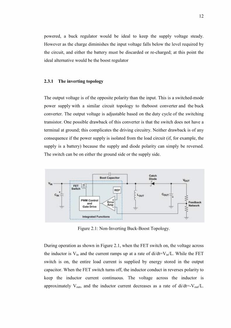
Figure 2.1: Non-Inverting Buck-Boost Topology.
During operation as shown in Figure 2.1, when the FET switch on, the voltage across
the inductor is Vin and the current ramps up at a rate of di/dt=Vin/L. While the FET
switch is on, the entire load current is supplied by energy stored in the output
capacitor. When the FET switch turns off, the inductor conduct in reverses polarity to
keep the inductor current continuous. The voltage across the inductor is
approximately Vout, and the inductor current decreases as a rate of di/dt=-Vout/L.

13
During the off time, the inductor supplies current both to the load and to replenish
the energy lost by the capacitor during the on time.
2.3.2 A buck (step-down) converter followed by a boost (step-up) converter
The output voltage is of the same polarity of the input, and can be lower or higher
than the input. Such a non-inverting buck-boost converter may use a single inductor
which is used for both the buck inductor and the boost inductor.
Like the buck and boost converters, the operation of the buck-boost is best
understood in terms of the inductor's "reluctance" to allow rapid change in current.
From the initial state in which nothing is charged and the switch is open, the current
through the inductor is zero. When the switch is first closed, the blocking diode
prevents current from flowing into the right hand side of the circuit, so it must all
flow through the inductor. However, since the inductor does not like rapid current
change, it will initially keep the current low by dropping most of the voltage
provided by the source. Over time, the inductor will allow the current to increase
slowly by decreasing its voltage drop. Also during this time, the inductor will store
energy in the form of a magnetic field.
CHAPTER 3
METHODOLOGY
3.1 Introduction
It is a well known fact that the most important step in the research process is to define
the problem as well as discussed the methods of study. Research methods are referring
to how the researcher gets the information and analysed the result based on the research
objective. At this point, the information and details of the flowchart sequence on how
the project is performed and an explanation of each step is also provided.
For this project, PSIM software is used to perform the simulations in order to
apply the construction of Buck-Boost converter. It has also used the Quartus II software
to construct the code for the controller. This project focuses on the design and
implementation of FPGA-based controller for Buck-Boost controller.

15
Figure 3.1: Project Flowchart
END
Literature review
START
Construct Converter
circuit
Write a Verilog code for controller
Upload to controller board
Hardware looping
Run
Analyze results.
Report Writing
NO
YES

16
Figure 3.1 shows that at the early stage, the project starts by gathering
information or literature research of the project. It starts by comparing the topologies for
the converter and then chooses the most suitable one. As a result of this research, a
suitable converter and the topologies is obtained to get the desirable results. All of the
activities are organized in the literature review part.
The next stage is writing the Verilog code and performing the compilation using
the Quartus II and doing the simulations in the PSIM software. Then, the converter was
constructed simultaneously with constructing the coding for the controller. If there is an
error, the coding needs to recheck and make the correction in order to produce good
output. Finally, the language is downloaded into the DE board and then the results are
discussed.
3.2 Development of FPGA-based controller algorithm.
A block diagram as shown in Figure 3.2 is basically the flow the FPGA
development for the controller algorithm. It consists of three main parts, writing Verilog
code for the switching controller, constructing the Buck-Boost converter and
implementation of Altera DE1 FPGA board. These three parts are the main systems that
will be focusing on this project. From figure below, it starting with builds a Verilog
description to control the switching points. It is important to match it with the design of
the controller system also with the hardware itself. Then, I/O pin assignment need to be
done to verify the port that needed to be use during the process. The wrong assign of pin
will cause the code to wrongly download to the board. Lastly, the physical
implementation is to make sure that the controller code design can successfully control
the controller of the Non-Inverting Buck-Boost converter.
Figure 3.2: FPGA implementation process.
Verilog
description
Place &
Route
FPGA I/O
assignment
Design
synthesis
Physical
implementation

As shown in Figure 3.3, the simulation of the converter is done using the PSIM
software. The desired output for the converter is 5V at 1A current rating.
non-inverting Buck-Boost converter is been chosen due to its wide input
applications and it can produce efficiency up to 90%. The PWM1 and PWM2 will be
replaced by the input controller in the hardware implementations. The
controller are N-MOSFET FQP5N
Figure 3.3: Simulation of Buck
Figure 3.
As shown in Figure 3.3, the simulation of the converter is done using the PSIM
software. The desired output for the converter is 5V at 1A current rating.
Boost converter is been chosen due to its wide input
applications and it can produce efficiency up to 90%. The PWM1 and PWM2 will be
replaced by the input controller in the hardware implementations. The
MOSFET FQP5N50C.
Figure 3.3: Simulation of Buck-Boost DC-DC Converter
Figure 3.4: Block diagram of the whole system.
17
As shown in Figure 3.3, the simulation of the converter is done using the PSIM
software. The desired output for the converter is 5V at 1A current rating. In this case, the
Boost converter is been chosen due to its wide input-voltage-range
applications and it can produce efficiency up to 90%. The PWM1 and PWM2 will be
replaced by the input controller in the hardware implementations. The switches for the
Converter
whole system.

18
Figure 3.4 shows the reference example used along the project. The power stage is a
non-inverting Buck-Boost converter with the following parameters: input voltage
Vout=5V, L=180µH, C=340µF, capacitor ESR (equivalent series resistance) RC=10kΩ,
and inductor DC resistance RL= 3.3kΩ. The input voltage has to be regulated at Vref=5V.
The output ADC is measured by using an ADC with full scale voltage. A second ADC is
used to close the loop of the system. This project describes a voltage control strategy,
where the voltage ADC converts the output voltage to a digital language. The error
between the desired and measured output voltage is processed by a digital controller to
determine the value of the switch duty ratio. The digital pulse modulator (DPWM)
generates the driving signals that control the Buck-Boost switches.
3.3 Switching configuration
The converter is improvised by the addition of the switch circuit switching
usually it uses a semiconductor switch (MOSFET / IGBT / transistor) for an ideal buck-
boost circuit (IBB) as the Figure 3.5 below, but the resulting output IBB thus inverting
the polarity opposite to the voltage source.
Figure 3.5: An Ideal Buck-Boost Converter

19
Figure 3.6: The series of Non-Inverting Buck-Boost converter.
To solve it and also improved efficiency so that added one additional switch on the
circuit non-inverting buck-boost (NIBB) using two switches buck (Sbuck) and boost
switches (Sboost) with two diodes buck (Dbuck) and the boost diode (Dboost) as shown
in Figure 3.6 above.
The switch configuration will determine the state of the converter whether it is
in Buck mode, Boost mode or even Buck-Boost mode. As shown in Table 3.1 below,
there are two switches that will control the mode.
Table3.1: The converter switching configuration.
Configuration Sbuck Sboost
Mode Buck Switching PWM1 OFF
Mode Boost ON Switching PWM2
Mode Buck-Boost Switching PWM1 Switching PWM2
Non-Inverting Buck-Boost (NIBB) circuit configuration settings done by adjusting the
PWM signal on Sbuck and Sboost depending on the input voltage, if the input voltage is
less than the set-point, then NIBB will work on boost mode, otherwise when the input

20
voltage is above the set-point value, then it will work on NIBB buck mode. And to
maintain the output voltage set-point (steady state) then NIBB will work in buck-boost
mode.
In buck mode, Sbuck will receive signals from the PWM1 switching signal,
while Sboost received the switching signal from PWM2 with the value of duty-cycle (D)
= 0, so the switch will open.Analysis of closed switches in buck mode; when Sbuck is
ON (close), Dbuck will be in reverse-biased state and Dboost is in forward-biased state,
then the inductor current will charge the supply load. Once the switch Sbuck is open
Dbuck and Dboost is both in forward-biased state, then the current stored in the inductor
will supply the load (discharging). With Vout value equation is as follows:
DinVoutV •= (3.1)
In boost mode, Sboost will receive switching signal PWM2, while Sbuck received signal
from PWM1 (duty-cycle = 1) and close.Analysis for the closed are as follows.When
Sboost is ON (close) Dboost and Dbuck are in reverse-bias state, so the current will fill
the inductor .Whereasin open switch, Sboost in open condition will trigger the Dbuck in
reverse-biased mode and Dboost in forward-biased mode, then the current stored in the
inductor will supply the load (discharging) coupled to the input voltage. With Vout
value equation is as follows:
inVD1
1outV ×
−
= (3.2)
In buck-boost mode, both switches Sbuck and Sboost received the switching signals
from PWM1 and PWM2. In the Figure 3.7, shows the buck-boost circuit with the
analysis of the closed switch which switches (Sbuck and Sboost) is ON (closed). This
will cause the diode buck (Dbuck) triggered in reverse-biased so that current will charge
the inductor L (charging) and inductor current (IL) raises to a maximum. With the
analysis formula enclosed switches are as follows:

21
×=
•=
dt
diLinV
LVinV
×=
onT
diLinV (3.3)
Figure 3.7: Closed switch analysis
Figure 3.8: Open switch analysis
In the Figure 3.8 above shows the buck-boost circuit with an open switch analysis where
both switches (Sbuck and Sboost) are OFF (open). The two diodes (Dbuck and Dboost)
22
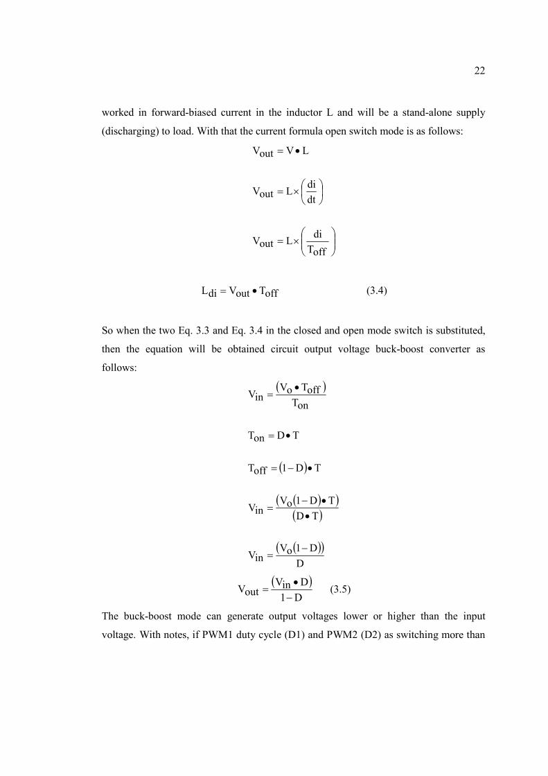
worked in forward-biased current in the inductor L and will be a stand-alone supply
(discharging) to load. With that the current formula open switch mode is as follows:
×=
×=
•=
offT
diLoutV
dt
diLoutV
LVoutV
offToutVdiL •= (3.4)
So when the two Eq. 3.3 and Eq. 3.4 in the closed and open mode switch is substituted,
then the equation will be obtained circuit output voltage buck-boost converter as
follows:
( )
( )
( )( )( )
( )( )D
D1oVinV
TD
TD1oVinV
TD1offT
TDonT
onT
offToVinV
−=
•
•−=
•−=
•=
•=
( )D1
DinVoutV
−•
= (3.5)
The buck-boost mode can generate output voltages lower or higher than the input
voltage. With notes, if PWM1 duty cycle (D1) and PWM2 (D2) as switching more than

23
Vin < 5V
50%, then the output voltage will be higher than the input voltage. If less than 50%, then
the output voltage will be lower than the input voltage.
3.4 Control system implementation on FPGA
The implementation of voltage control loops is determinate by the control
flowchart as shown in Figure 3.9.
Figure 3.9: Voltage control loop.
Vin = 5V
Vin > 5V
Start
Compare Vin
Boost Mode
ONbuckD
outV
inV1boostD
=
−=
Buck Mode
OFFboostD
inV
outVbuckD
=
=
Read Vin& Read Vout
End
Buck-Boost Mode
inV
outVbuckD
outV
inV1boostD
=
−=
Output
Duty Cycle

24
For the control voltage loop, the design must be considering the value of input that will
be inserted. The main goal of this system is to produce the 5volt output, fix no matter
how high or how low the input is. In this project, the range for testing is limited from
0volt to 10volt but the density of this prototype is until 15volt. The starting of this
system is the board will firstly read the value of input inserted to the converter. It will
automatically calculate in the program either to buck or boost the value to get the output
of 5volt. If the input is less than 5volt, the Boost mode will trigger. The Sboost will
switching and the Sbuck will be in ON condition. When the input is more than 5volt, it
will change to Buck condition where Sbuck will switch and the Sboost will be off. If the
input is set at 5volt, this will cause the converter to operate in Buck-Boost mode to
maintain the value. Both switch will be switching and resulted the output value of 5volt.
3.4.1 Analog-digital conversion
Taking into account the high switching frequency, the time limitations in the control
method and the small current ripple, an ADC with a wide bandwidth is required. The
ADC0804 is a CMOS 8-bit stand alone operator, 10 kSPS sample rate.
In analog-to-digital converter (ADC) accepts an analog input a voltage or a
current and coverts it to a digital value that can be read by a microprocessor. Figure 3.10
below shows a simple voltage-input ADC. It has one input, an 8-bit digital word that
represents the input value.
52
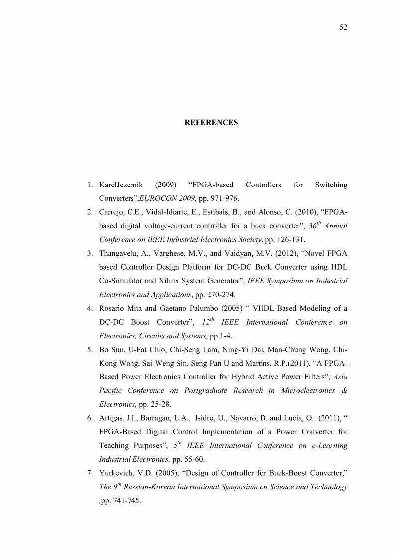
REFERENCES
1. KarelJezernik (2009) “FPGA-based Controllers for Switching
Converters”,EUROCON 2009, pp. 971-976.
2. Carrejo, C.E., Vidal-Idiarte, E., Estibals, B., and Alonso, C. (2010), “FPGA-
based digital voltage-current controller for a buck converter”, 36th Annual
Conference on IEEE Industrial Electronics Society, pp. 126-131.
3. Thangavelu, A., Varghese, M.V., and Vaidyan, M.V. (2012), “Novel FPGA
based Controller Design Platform for DC-DC Buck Converter using HDL
Co-Simulator and Xilinx System Generator”, IEEE Symposium on Industrial
Electronics and Applications, pp. 270-274.
4. Rosario Mita and Gaetano Palumbo (2005) “ VHDL-Based Modeling of a
DC-DC Boost Converter”, 12th IEEE International Conference on
Electronics, Circuits and Systems, pp 1-4.
5. Bo Sun, U-Fat Chio, Chi-Seng Lam, Ning-Yi Dai, Man-Chung Wong, Chi-
Kong Wong, Sai-Weng Sin, Seng-Pan U and Martins, R.P.(2011), “A FPGA-
Based Power Electronics Controller for Hybrid Active Power Filters”, Asia
Pacific Conference on Postgraduate Research in Microelectronics &
Electronics, pp. 25-28.
6. Artigas, J.I., Barragan, L.A., Isidro, U., Navarro, D. and Lucia, O. (2011), “
FPGA-Based Digital Control Implementation of a Power Converter for
Teaching Purposes”, 5th IEEE International Conference on e-Learning
Industrial Electronics, pp. 55-60.
7. Yurkevich, V.D. (2005), “Design of Controller for Buck-Boost Converter,”
The 9th Russian-Korean International Symposium on Science and Technology
,pp. 741-745.

53
8. Konishi, Y., Huang, Y.F. (2007), “ Soft-Switching Buck Boost Converter
Using Pulse Current Regenerative Resonant Snubber”,29th International
Telecomunications Energy Conference, pp. 886-890.
9. Vineeta Agarwal and Anupam Kumar (2007), “SiC Based Buck-Boost
Converter”, International Power Engineering Conference, pp. 1014-1017.
10. Olranthichachat, P., Saenthon, A., and Kaitwanidvilai, S. (2008), “ Genetic
Algorithm Based Fixed-Structure H Loop Shaping Control of a Buck-Boost
Converter”, IEEE International Conference on Robotics and Biomimetics, pp.
1944-1949.
11. Delshad, M., Farzanehfard, H., (2010), “ A New Isolated Bidirectional Buck-
Boost PWM Converter”, 1st Power Electronics & Drive Systems &
Technologies Conference, pp. 41-45.
12. Orellana, M., Petibon, S., Estibals, B., and Alonso, C. (2010), “Four Switch
Buck-Boost Converter for Photovoltaic DC-DC Power Applications”, 36th
Annual Conference on IEEE Industrial Electronics Society, pp. 469-474.
13. Ray-Lee Lin and Rui-Che Wang(2010), “Non-Inverting Buck-Boost Power-
Factor-Correction Converter with Wide Input-Voltage_range Applications”,
36th Annual Conference on IEEE Industrial Electronics Society, pp. 599-604.
14. Boopathy, K. (2011), “A Novel Method of Implementing Real-Time Buck-
Boost Converter with Improved Transient Response for Low Power
Applications”, IEEE Symposium on Industrial Electronics & Applications,
pp. 150-160.
15. Bo-Han Hwang, Bin-Nan Sheen, Jiann-Jong Chen, Yuh-Shyan Hwang and
Cheng-Chieh Yu (2012), “ A Low-Voltage Positive Buck-Boost Converter
using Average-Current-Controlled Techniques”, IEEE International
Symposium on Circuits & Systems, pp. 2255-2258.
16. Chin-Hong Chen, Chia-Ling Wei and Kuo-Chun Wu (2012) “Integrated Non-
Inverting Buck-Boost DC-DC Converter with Average-Current-Mode
Control”, IEEE International Conference on Circuits & Systems, pp. 6-9.
17. Juan Carlos Ostos, Dylan Dah-Chuan Lu (2012) “Modeling and Analysis of
CCM Non-Isolated High Step-Up Interleaved Buck-Boost DC-DC
Converters”, IEEE International Conference on Power &Energy , pp 28-31.
54
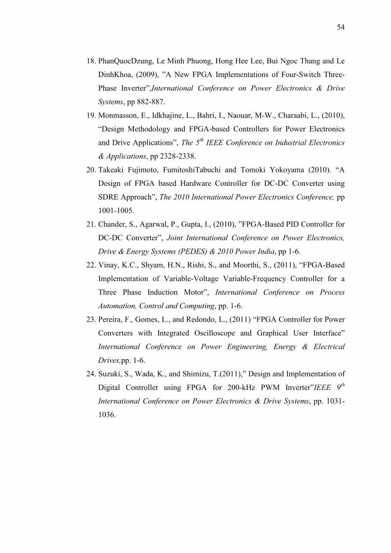
18. PhanQuocDzung, Le Minh Phuong, Hong Hee Lee, Bui Ngoc Thang and Le
DinhKhoa, (2009), ”A New FPGA Implementations of Four-Switch Three-
Phase Inverter”,International Conference on Power Electronics & Drive
Systems, pp 882-887.
19. Monmasson, E., Idkhajine, L., Bahri, I., Naouar, M-W., Charaabi, L., (2010),
“Design Methodology and FPGA-based Controllers for Power Electronics
and Drive Applications”, The 5th IEEE Conference on Industrial Electronics
& Applications, pp 2328-2338.
20. Takeaki Fujimoto, FumitoshiTabuchi and Tomoki Yokoyama (2010). “A
Design of FPGA based Hardware Controller for DC-DC Converter using
SDRE Approach”, The 2010 International Power Electronics Conference, pp
1001-1005.
21. Chander, S., Agarwal, P., Gupta, I., (2010), ”FPGA-Based PID Controller for
DC-DC Converter”, Joint International Conference on Power Electronics,
Drive & Energy Systems (PEDES) & 2010 Power India, pp 1-6.
22. Vinay, K.C., Shyam, H.N., Rishi, S., and Moorthi, S., (2011), “FPGA-Based
Implementation of Variable-Voltage Variable-Frequency Controller for a
Three Phase Induction Motor”, International Conference on Process
Automation, Control and Computing, pp. 1-6.
23. Pereira, F., Gomes, L., and Redondo, L., (2011) “FPGA Controller for Power
Converters with Integrated Oscilloscope and Graphical User Interface”
International Conference on Power Engineering, Energy & Electrical
Drives,pp. 1-6.
24. Suzuki, S., Wada, K., and Shimizu, T.(2011),” Design and Implementation of
Digital Controller using FPGA for 200-kHz PWM Inverter”IEEE 9th
International Conference on Power Electronics & Drive Systems, pp. 1031-
1036.