december 2002 classification definitions 257 … · december 2002 classification definitions 257...
TRANSCRIPT

December 2002 CLASSIFICATION DEFINITIONS 257 - 1
CLASS 257, ACTIVE SOLID-STATE DEVICES(E.G.,TRANSISTORS, SOLID-STATEDIODES)
SECTION I - CLASS DEFINITION
This class provides for active solid-state electronicdevices, that is, electronic devices or components thatare made up primarily of solid materials, usually semi-conductors, which operate by the movement of chargecarriers - electrons or holes - which undergo energylevel changes within the material and can modify aninput voltage to achieve rectification, amplification, orswitching action, and are not classified elsewhere.
SCOPE OF THE CLASS
Active solid-state electronic devices include diodes,transistors, thyristors, etc., but exclude pure resistors,capacitors, inductors, or combinations solely thereof.The latter class of devices is characterized as passive.
The subject matter to be found here includes only activesolid-state devices, per se. It may include one or moresuch devices combined with contacts or leads, or struc-tures configured to be tested on a semiconductor chip, ormerely semiconductor material without contacts orleads where the sole disclosed use is an active solid-state device. This subject matter does not include activesolid-state devices combined with significant circuits.
Claims reciting an integrated circuit nominally with sig-nificant metallization will be classified in Class 257,whereas otherwise, nominal recitation of an integratedcircuit (i.e., without significant active solid-state devicerecitation) will not be sufficient to permit the device tobe classified in Class 257.
KEY CONCEPTS
See Subclass References to the Current Class, below, forreferences that relate to key concepts and terms found inClass 257. An indication that a particular concept orterm occurs in one or more subclasses does not meanthat the indicated subclass or subclasses are the onlyplaces that subject matter may be found. That subjectmatter may possibly be found elsewhere in Class 257listed under a related term or concept that may bebroader or narrower or of the same scope.
OTHER CLASSIFICATION SYSTEMS
Each subclass definition may contain an OTHERCLASSIFICATION SYSTEMS listing that is to be used
for informational purposes only. These classificationlistings may change at any time after their publicationand are therefore not guaranteed to be current. In addi-tion, the classification listing does not necessarily indi-cate the sole relationship between the U.S. PatentClassification System and foreign classifications. Evenwhere a single classification is listed for a single U.S.subclass, a one-to-one correlation should not beinferred. As a result, information contained therein isconsidered to be only a guide to related subject matter.
SECTION II - LINES WITH OTHER CLASSESAND WITHIN THIS CLASS
A. Classes related to Class 257 subject matter in thesense that they employ active solid-state devices in elec-tronic circuits and the relationship of these classes toClass 257 is mainly that of a combination to a subcom-bination or of a genus to a specie. See References toOther Classes, below, referencing this section.
B. Classes related to Class 257 subject matter in thesense that they employ active solid-state devices in elec-tronic circuits and the use of active solid-state electronicdevices primarily as a perfecting feature. See Refer-ences to Other Classes, below, referencing this section.
C. See References to Other Classes below for classesthat provide for materials used in active solid-state elec-tronic devices.
D. See References to Other Classes, below, for classesrelated to Class 257 because they provide for methodsof making, cleaning, coating, etc., active solid-statedevices, e.g., Class 438, Semiconductor Device Manu-facturing: Process.
E. See References to Other Classes, below, for Classesrelated to Class 257 because they provide for activesolid-state electronic devices structures with a specifieduse, e.g., Class 136, Batteries: Thermoelectric and Pho-toelectric.
F. See References to Other Classes, below, for classesproviding for provide for subcombination subject mat-ter that can be used as component part of active solid-state electronic devices (e.g., lead frames) or perfect thedevice (e.g., a heat sink).
G. Classes which provide for passive solid-state elec-tronic devices with names that may refer to either activeor passive solid-state electronic devices, e.g., coherers,varistors, varactors. luminescent or electroluminescent
December 2002 Edition
257 - 2 CLASSIFICATION DEFINITIONS December 2002
devices. The devices may be part of the main subjectmatter of the class or may be used as circuit elements incircuits or control or measuring systems which form themain subject matter of the class.
See References to Other Classes, below, referencing thissection.
SECTION III - SUBCLASS REFERENCES TOTHE CURRENT CLASS
SEE OR SEARCH THIS CLASS, SUBCLASS:1 through 8, for bulk effect device.2 - 5, 16, 52-63, and 646, for amorphous semi-
conductor material.4 72, 91, 144, 150, 151, 175-177, 181, 182, 207-
211, 246-250, 276, 309, 317, 401, 448, 457,459, 503, 508, 573, 584, 587, 602, 621, 625,666-676, and 692-697, for configuration ofelectrode, contact, lead or pad.
4 32, 33, 81, 91, 99, 144, 150-153, 177-179, 181,182, 203, 207-211, 276, 377, 382-385, 459,503, 522, 554, 573, 576, 584, 602, 621, 625,661-677, 690-700, and 734-786, for electricalcontact or lead.
6 through 8, for Gunn effect (intervalley trans-fer).
7 for intervalley transfer (e.g., Gunn) device inintegrated circuit.
10 through 11, and 407, for controlled work func-tion material.
10 and 11, for electron emissive layer. 10 through 27, and 104-106, for heterojunction
involving quantum-mechanical tunneling.10 and 11, for photocathode.10 54, 73, 155, 192-195, 217, 260, 267, 269, 275-
277, 280-284, 449-457, 471-486, and 928, forSchottky barrier.
10 11, 30-39, and 314-326, for tunneling-insulatorlayer.
10 11, and 407, for work function of material, con-trolled, e.g., low.
13 76, 78, 85, 90, and 94-97, for heterojunctionlight emitter.
13 79-103, and 918, for light emitting device.13 through 25, for quantum well device.15 through 22, and 28, for superlattice.16 55, 63, and 65, for heterojunction in non-sin-
gle-crystal material.18 19, and 190, for mismatched or strained lattice.18 19, and 190, for mismatch of lattice constant.18 and 19, for strained layer superlattice hetero-
junction.
19 76, 78, 103, 200-201, and 613-616, for alloy oftwo different semiconductors (e.g., GaxIn1-
xAs).
20 24, 27, 57-61, 66-72, 133-145, 192-195, 202-211, 213, and 252-413, for field effect devices.
20 24, and 194, for HEMT (High electron mobil-ity transistor).
20 27, 187, and 192-195, for heterojunction FETs.21 85, 184-189, for heterojunction in light respon-
sive device.21 for light responsive or activated device (super-
lattice quantum well heterojunction).21 53-56, 59, 72, 80-85, 113-118, 184-189, 222,
223, 225-234, 257, 258, 290-294, 325, 428-466, 680, 681, and 749, for radiation respon-sive.
21 and 187, for light responsive heterojunctiontransistor.
21 187, 443, and 462, for photosensitive bipolartransistor.
26 27, and 29, for ballistic transport device.26 27, and 29, for ballistic transport transistor.31 through 36, for Josephson device.31 through 36, and 661-663, for superconductive
element/device. 31 through 36, 468, and 661-663, for thermal
device operated at cryogenic temperature.33 for high temperature (30 K) Josephson device.40 for organic semiconductor material.41 for point contact device.42 for Selenium (elemental).44 through 47, for alloyed junction.45 for thermal gradient zone melting (TGZM).46 104, and 105, for Esaki diode.46 and 104-106, for p-n junction type (Esaki type)
tunneling.47 197, 205, 273, 350, 361, 370, 378, 423, 462,
477 though 479, 511, 512, 517, 518, 525, 526,539-543, and 552-593, for bipolar transistorstructure.
47 for alloyed junction bipolar transistor.48 and 797, for calibration or test structure.5, for
array of bulk effect amorphous switches.48 for test structures. 49 through 75, for non-single crystal, as active
layer.49 through 51, 64-75, 359, 377, 380-382, 385,
412, 505, 518, 520, 524-527, 538, 554, 576,581, 588, and 754-757, for polycrystallinesemiconductor material.
49 through 51, and 64-75, for polycrystallineactive junction material.
1December 2002 Edition

December 2002 CLASSIFICATION DEFINITIONS 257 - 3
49 through 51, and 64-75, for recrystallized activesemiconductor layer.
50 and 530, for anti-fuse component or element.50 530, and 928, for shorted devices, in general,
e.g., anti-fuse elements.53 through 56, for amorphous semiconductor
material device.53 through 56, 108, 225, 252, and 414, for respon-
siveness to nonelectric signal.55 and 63, for alloy of amorphous semiconductor
materials.55 63, and 65, and 646, for silicon nitride to
increase band gap of amorphous or polycrystal-line silicon.
56 58, 62, and 65, for for dangling bond.56 58, 62, and 68, for passivation of dangling
bonds in nonsingle crystal semiconductor.57 through 61, 66-72, and 368-401, for insulated
gate FET in integrated circuit.57 through 61, and 66-72, for FET in non-single
crystal or recrystallized semiconductor mate-rial (e.g., amorphous or polycrystalline semi-conductor as channel).
59 72, and 88-93, for array as imager, or withtransparent electrode, or as display (with plurallight emitters).
59 72, 449-457, and 749, for electrical contact orlead transparent to light.
59 72, and 293, for photoresistor combined withaccessing FET.
59 72, 453, and 749, for transparent electrode.60 135, 136, 263-267, 302, and 328-334, for verti-
cal channel field effect device.64 255, 521, 627, and 628, for crystal axis or
plane.65 for alloy of polycrystalline semiconductor
materials.66 67, 69, 379-381, 903, and 904, for static mem-
ory cell using FET. 67 through 70, for stacked FETs. 67 69, 70, and 74, for stacked FETs.68 through 71, 296-313, 296, 298, 300, 906, and
908, for capacitance combined with insulatedgate device. (e.g., DRAM).
68 71, and 295-313, for insulated gate device(capacitor or combined with capacitor).
68 71, 296-313, and 905-908, for memory devicecomponent involving a capacitor (e.g.,dynamic memory cell).
68 71, 303, and 306-309, for stacked capacitors inDRAM cell.
68 and 301-305, for capacitor in trench.
68 283, 284, 330-334, 374, 397, 513, 514, 622,647, and 648, for vertical walled groove insemiconductor.
69 195, 204, 206, 338, 350, 351, 357-359, and365-377, for CMOS.
69 195, 204, 206, 274, 338, 350, 351, 357-359,and 369-377, for complementary field effecttransistors.
74 and 278, for three-dimensional integrated cir-cuit.
76 through 78, and 183-201, for heterojunction,generally.
76 through 78, for wide band gap semiconductormaterial other than GaAsP or GaAlAs.
80 through 85, for light responsive or activateddevice combined with light emitting device.
81 99, 177-181, 584, 625, 675, 688, 689, 705, 707,712-722, and 796, for heat sink.
81 82, and 99, for housing or package for lightemitter.
81 and 82, for housing or package for light emit-ter combined with light receiver.
81 82, 433, 434, 680, 681, for housing or packagefor light responsive device.
81 99, and 666-677, for lead frame.83 for light coupled transistor structure.86 and 87 for indirect band gap active layer - light
emitter.87 131, 156, 439, 523, 590, and 608-612, for deep
level dopant/impurity.87 126, 131, 156, 523, 590, 609-612, and 617, for
recombination centers.91 98, 151, 175, 176, 249, 250, 276, 282-284, 309,
317, 401, 418, 435, 448, 457, 459, 503, 508,534, 573, 587, 602, 621, 662, and 664, forshape(d) contact, electrode, conductor, or ter-minal.
91 98, 294, 323, 435, and 659, for optical shield.93 for plural light emitters in integrated circuit.93 374, 446, 499 and 564, for electrical isolation
of components in integrated circuit.95 117, 118, 127, 170, 244, 283, 284, 301-305,
330-334, 418, 419, 447, 460, 466, 496, 534,571, 586, and 618-628, for grooves, generally.
95 170, 171, 452, 466, 496, 571, 586, 594, 600,618, and 623-626, for mesa structure.
95 for shaped contact, electrode, etc., external ofheterojunction light emitter.
98 116, 117, 294, and 432, for light fiber, guide, orpipe.
98 for luminescent material used with light emit-ter.
98 181, 418, 688, 710, 711, 728, and 730, forshaped housing or package.
December 2002 Edition
257 - 4 CLASSIFICATION DEFINITIONS December 2002
98 99, 116, 434, 680, and 681, for window (opti-cal) for housing.
100 433, 434, 667, 687, 767-and 796, for encapsu-lated.
101 194, 219-221, 264, 269, 285, 335-345, 404,430, 450, 458, 463, 492, 493, 497, 498, 543,545, 548, 558, 583, 591, 592, 596, 597, 605,606, 655-657, 927, and 929, for dopant/impu-rity concentration, incl., graded profile.
102 227, 439, and 607-612, for specified, generally(e.g., photoionizable).
106 for reverse conducting diode (tunnel diode).106 for Zener diode. 107 through 182, and 918, for regenerative switch-
ing device.108 252, and 421-427, for magnetic field respon-
sive.108 225, 254, and 415 and-419, for device respon-
sive to pressure.108 222, 225, 254, and 417-419, for strain sensor.108 225, 252, and 467-470, for passivating device
responsive to temperature.109 for Shockley diode.110 and 119-131, for bidirectional device (diac,
rectifier).113 through 118, for regenerative-type switching
device.115 123, and 157-161, for amplified gate in thyris-
tor.121 for reverse conducting thyristor.121 for Static Induction Transistor (SIT) - Bipolar
transistor as reverse path of bidirectional con-ducting thyristor.
122 141, 146, and 162, for lateral structure inregenerative device.
124 125, and 133-145, for FET in or combined withthyristor.
125 137, 138, 143, and 149, for shunt, regenerativedevice.
125 137, 138, 143, 149, and 154, for shorted emit-ter, anode or cathode, in thyristor.
127 446, 510-522, 571, 577, and 594, for groove todefine plural devices.
127 170, 339, 372-376, 394-400, 409, 452, 484,490, 493-495, and 605, for guard ring orregion.
131 156, 376, 424, 523, 590, and 617, for crystaldamage.
133 145, 195, 205, 273, 337, 350, 361, 362, 370,and 378, for field effect combined with bipolartype (including regenerative type) device.
134 through 136, 217, 256-287, and 504, for JFET.136 205, 264, 268, 269, 392, for enhancement
mode.
139 through 145, and 212, for conductivity modu-lated transistor.
139 through 145, 147-153, for extended latchingcurrent device.
139 through 145, 147-153, and 372-376, for meansto prevent latchup.
139 through 145, and 211, for conductivity modu-lated transistor.
142 148, 376, 553, and 583, for doping for gainreduction.
146 476-479, and 499-564, for structure with elec.isolated components.
150 151, 177-181, for housing or package forregenerative type switching device.
154 169, 194, 195, 218, 264, 523, 646, and 656, forhigh resistivity semiconductor region - see,also, intrinsic material; PIN device.
154 350, 358, 359, 363, 379-381, 516, 533, 536-543, 571, 572, 577, 580-582, and 904, forresistive element (resistor) (passive device).
164 and 580-582, for ballasting of current (e.g., byresistors).
164 through 166, 560-561, 563, and 579- 581, formultiple/plural emitter.
170 for edge, beveled - preventing breakdown.171 496, 586, and 618+, for bevel.171 452, 483, and 484, for protection against edge
breakdown.171 and 496, for reverse bevels.173 174, 328, 355-363, 487-496, and 546, for pro-
tection against overcurrent or overvoltage.173 529, 665, and 910, for fuse/fusible link.173 for overvoltage protection means in thyristor.177 through 181, 467, 468, 573, 625, 675, 688,
705-707, and 712-722, for cooling.178 179, and 746-748, for stress avoidance between
electrode and semiconductor.178 through 179, 633, 747, and 748, for thermal
expansion matching or compensation.180 and 733, for stud-type mount for housing.180 and 733, for stud mount.181 182, 688, 689, 726, 727, and 785 for press con-
tact of electrode and semiconductor.183.1, 193 215-251, and 912, for charge transfer
device. 184 through 189, for heterojunction.185 and 191, for graded band gap.185 for staircase (light responsive heterojunction). 187 197, and 198, for heterojunction bipolar tran-
sistor.198 for wide band gap emitter heterojunction bipo-
lar transistor.199 481, 482, 551, and 603-606, for avalanche
diode.
1December 2002 Edition

December 2002 CLASSIFICATION DEFINITIONS 257 - 5
199 482, and 604, for IMPATT.199 259, 275-277, 482, 523, 604, 624, 625, 659,
662, 664, and 728, for for microwave devicecomponent.
202+, and 909, for master slice (gate array).202+, and 909, for gate arrays.202 through 211, and 909, for gate arrays.205 273, 350, 361, 370, and 378, for bipolar com-
bined with field effect type device.205 273, 350, 361, 370, and 378, for bipolar tran-
sistor structure combined with FET.206 208, 210, and 211, for configuration of ele-
ments in gate array.209 for gate array with programmable signal paths.210 and 758-760, for multi-level metallization.212 for double-base diode (unijunction transistor).212 for Static Induction Transistor (SIT) - Unijunc-
tion transistor.212 for unijunction transistor.214 for charge injection device.215 218, and 225-251, for surface channel charge
transfer device.216+, for bulk channel device.216 and 285, for buried channel.219 through 221, for nonuniform channel doping in
buried channel CCD.223 230, and 445, for antiblooming.223 230, and 445, for suppression of blooming in
light imager.224 and 243, for channel confinement.225 253, and 414, for chemical sensor. 225 for CCD with fixed pattern memory as ROM.228 447, 460, for backside illumination. 239 for floating diffusion as CCD Output Tap. 239 261, and 315-323, for floating gate.240 for nonuniform channel thickness in CCD.241 for parallel channels in CCD. 245 364, and 489, for resistive electrode.246 through 248, for nonuniform channel doping in
CCD, for directionality.249 317, 359, 363, 364, 377, 380-382, 384, 385,
387, 407, 412, 413, 489, 505, 518, 520, 524-527, 538, 554, 576, 581, 588, 646, 754-756,904, and 914, for polycrystalline material(including polysilicon contacts) other thanactive junction material.
251 for bucket-brigade device.254 and 416, for acoustic energy detector.256 and 257, for light responsive PIN device com-
bined with JFET.257 and 258, for JFET.227 and 439, for photoionization.258 291-294, 443-448, and 911, for array of elec-
trode field effect devices.
260 and 262, in or combined with a JFET device.260 and 261, for memory device component
involving a JFET (e.g., taper isolated or float-ing pn junction gate type).
265 for vertical current path JFET in integrated cir-cuit.
266 267, and 287, for parallel channels in JFET.269 and 285, for nonuniform channel doping in
JFET.272 through 278, for JFET in integrated circuit.275 through 278, 662, and 664, for stripline lead. 276 for air bridge electrical lead.276 for air bridge contact.283 and 284, for groove alignment of Schottky gate
to source region in MESFET.283 through 284, 330-334, for gate electrode of
FET formed in groove.286 for nonuniform channel thickness in JFET.290 and 294, for IGFET.291 through 294, 326, 334, 337, 338, 347-363, and
368-401, for insulated gate device (IGFET inintegrated circuit).
294 297, 340, 409, 435, 488-490, 503, 508, 630,659-660, and 662, for shield electrode.
295 298, and 314-326, for EPROM/EEPROM.295 298, 314, and 324-326, for MNOS insulated
gate-type memory device component.297 349, 547, and 620, for means to prevent charge
leakage or leakage current. 297 349, 354, 372-376, 503, 547, and 620, for
means to prevent leakage current or chargeleakage.
297 660, and 921, for protection against radiation(e.g., alpha particles).
297 660, and 921, for radiation protection.297 422, and 659-660, for ionizing radiation shield,
charged particles, electric or magnetic fields.298 and 315-326, for insulated gate device (floating
gate memory device).298 and 315-323, for floating insulated gate mem-
ory-type memory device component.299 for substrate bias (electrical generator.301 through 305, 534, and 599, for groove involv-
ing a capacitor.305 354, 376, 398-400, 519, 620, 648, and 652, for
channel stop.305 333, 374, 389, 395-399, 510-521, and 632-651,
for field oxide.312 480, and 595-602, for voltage variable capaci-
tance device.314 through 326 for variable threshold insulated
gate device (e.g., EEPROM, non-volatile mem-ory MOSFET).
December 2002 Edition

257 - 6 CLASSIFICATION DEFINITIONS December 2002
322 for programming of floating gate MISFET(avalanche breakdown).
323 680, and 681, for light erasure of EPROM.325 for oxynitride as insulator in MNOS memory
IGFET.327 through 346, for short channel.328 and 355-363, for overvoltage protection means
in IGFET.328 and 355-363, for MOSFET gate protection.331 341, 342, and 401, for parallel channels in
IGFET.332 346, 387, 388, 412, and 413, for self-aligned
MOSFET gate. 333 340, and 386-389, for reduction of gate capaci-
tance (FET).333 346, 387, and 388, for overlap of gate electrode
with source or drain in IGFET.334 337, and 338, for VMOS or DMOS short
channel IGFET in integrated circuit.336 344, 408, and 900, for LDD (lightly doped
drain) device.339 409, 483, 484, and 487-496, for preventing
avalanche breakdown.339 409, and 488-490, for field relief electrode.339 409, 490, and 495, for floating pn junction
guard region.340 394, and 630, for field shield electrode.345 and 404, for nonuniform channel doping in
IGFET. depletion mode.347 through 354, and 507, for insulating substrate
integrated circuit.347 through 354, and 507, for single crystal insulat-
ing substrate. 347 through 354, and 507, for single crystal semi-
conductor layer on insulating substrate (SOI).348 391, 392, and 402-407, for depletion mode
Insulated Gate FET.349 354, 372-376, 503, and 547, for controlling,
reducing, etc. parasitics.350 511, 512, 525, and 555-562, for lateral bipolar
transistor in integrated circuit.354 through 374, 395-399, 501, and 506-527, for
dielectric isolation.355 through 363, for gate insulator breakdown pro-
tection in IGFET integrated circuit.360 and 367, for insulated gate device (controlling
pn junction breakdown).361 362, and 497-499, for punch-device.366 for overlap of plural gate electrodes in IGFET.368 through 401, for PN junction isolation in MOS-
FET integrated circuit.374 394-398, 626, 631-651, and 758-760, for insu-
lating/passivating coating.
374 396-398, 510-521, 647, and 648, for groove(dielectric isolation means).
377 382-385, 388, 412, 413, 454-458, 486, 518,554, 576, 588, 747, 748, 754-757, 761, 763-764, and 768-770, for refractory electrodematerial.
377 382-384, 388, 412, 413, 454-456, 485, 486,576, 587, 751, 754-757, and 768-770, for sili-cide.
379 through 381, and 903-904, for static RAMarrangement.
379 through 381, 516, 528-543, 903, 904, 919, and924, for passive components in integrated cir-cuits.
382 through 384, 576, 757, 768, and 769, for metalor silicide of platinum group metal, as ohmiccontact.
383 388, 412, 485, 486, 763, 764, and 770, for pureor alloyed titanium.
388 407, 412, and 413, for metal or silicide of plati-num group metal, as MOSFET gate.
390 and 391, for array of IGFETs.390 and 391, for nonerasable (e.g., ROM).390 and 391, for mask-programmed MOSFET
ROM.401 for nonuniform channel thickness in IGFET.410 411, 639-641, 649, and 760, for silicon nitride.411 and 760, for composite insulator material.411 for oxynitride as gate insulator in IGFET, in
general.422 and 659, for magnetic field shielding423 511, 512, 525, 526, 556, 557-562, 575, and
576, for lateral bipolar transistor structure.423 for magnetic field sensing bipolar transistor.426 and 469, for passivating means to reduce tem-
perature sensitivity. 427 for magnetic field sensor in integrated circuit.430 and 458, for light or radiation responsive PIN
device, in general.431 466, for light responsive or activated device
generally.437 for anti-reflection coating.444 for matrix or array of light sensor elements
overlying active switching elements in inte-grated circuit.
446 for matrix or array of light sensors with spe-cific isolation means in integrated circuit.
449 through 457, for Schottky barrier.453 through 455, 485, and 486, for metal or silicide
of platinum group metal, as Schottky barriermaterial.
458 523, 538, and 656, for intrinsic material orregion.
458 for PIN diode.
1December 2002 Edition

December 2002 CLASSIFICATION DEFINITIONS 257 - 7
459 676, and 786, for bonding flag or pad465 592, 599, 653, and 654, for configuration of
junction geometry.466 496, 571, 586, 594, 599, 600, and 618-628, for
configuration of external portion of activedevice.
474 for bipolar transistor with Schottky barriertransistor as emitter-base or base-collectorjunction.
474 through 479, 512, 525, 555, 556, and 574-576,for integrated injection logic.
477 through 479, for bipolar transistor in integratedcircuit with Schottky barrier diode.
479 and 570, for anti-saturation diode.479 for baker clamp.486 740, 751, and 767, for diffusion barrier.491 and 492, for means to increase breakdown volt-
age in integrated circuit.492 and 493, for RESURF device. 494 for reverse biased (electrical) pn junction guard
region.494 for reverse biased guard ring to prevent break-
down.497 and 498, for punchthrough transistor.504 for JFET isolation in integrated circuit (i.e.,
pinched-off region used for integrated circuitisolation).
509 through 521, 544-556, and 929, for isolatedPN junction.
509 through 521, for PN junction isolation in inte-grated circuit combined with dielectric isola-tion.
511 512, 525, 555, 556, 569, and 574-576, for com-plementary bipolar transistor structure.
511 512, 525, 555, 556, 569, and 574-576, for com-plementary bipolar transistors.
511 512, 514, 515, 517, 518, 525, 526, 539-543,and 552-563, for bipolar transistors in inte-grated circuit.
511 512, 514, 517, 518, and 552-556, for bipolartransistors with pn junction isolation.
512 569, and 574-576, for bipolar transistor struc-ture with common active region.
512 569, and 574-576, for complementary bipolartransistors with common active region.
512 555, 556, and 574-576, for logic device (super-integrated) using Integrated Injection Logic
(I2L).514 and 515, for walled emitter bipolar transistor.522 for air isolation of integrated circuit.531 for inductance in integrated circuit.532 through 535, for capacitance as passive compo-
nent in non-FET I.C.
540 for dynamic isolation pocket bias (electrical).541 for pinch resistor.544 through 556, for PN junction isolation in inte-
grated circuit in general.545 for reduction of isolation junction capacitance.546 for overvoltage protection means in pn junction
isolated integrated circuit.546 for reverse voltage polarity protection, in pn
junction isolated integrated circuit.549 for collector diffused type isolation.559 lateral transistor formed along groove.560 through 564, for multiple/plural collectors. 560 563, and 579-581, for plural emitters in bipolar
transistor.562 for logic device (superintegrated) using Cur-
rent Hogging Logic (CHL).565 through 593, for bipolar transistor structure, in
general.571 for groove resistor in Darlington bipolar
device.573 and 584, for housing or package for bipolar
transistor devices.592 for configuration of bipolar transistor base
region.602 for housing or package for voltage-variable
capacitance device.607 and 917, for plural dopants of same conductiv-
ity type.610 for platinum (as deep level dopant).620 for scribe line or region.624 for prevention of skin effect, microwave
device, by low resistance ohmic contact alongmesa surface.
626 and 629-652, for passivation of semiconductorsurface.
634 for passivating glass with ingredient to adjustsoftening or melting temperature.
639 and 649, for oxynitride as passivating insulat-ing layer.
642 643, and 759, for organic insulating material orlayer.
643 759, and 788, for polyamide.643 759, and 792, for polyimide.653 654, for shaped PN junction. 655 for reverse doping concentration gradient pro-
file.656 for PIN device in general.657 for stepped profile.657 for stepped dopant concentration profile.660 for housing or package for radiation shielded
device.662 and 664, for transmission line lead.663 for superconductive contact or lead on inte-
grated circuit.
December 2002 Edition

257 - 8 CLASSIFICATION DEFINITIONS December 2002
669 670, 673, 674, 676, 688, 689, 692-697, 728,735-739, 752, 758, 773-776, and 780-786, forshaped contact, electrode, etc.
669 for lead frame having stress relief. 676 for die bonding flag.676 for lead frame-type mount for chip.678 through 733, for housing or package, generally.679 and 922, for smart card (e.g., “credit card” inte-
grated circuit package). 686 for stacked housings. 700 701, and 703-707, for ceramic housing or pack-
age material.705 for high thermal conductivity ceramic for
package.711 for metal housing with mount for chip.713 for cooling of housing or contents for inte-
grated circuit.714 through 716, for liquid coolant.719 for press contact of heat sink and semiconduc-
tor.720 for high thermal conductivity insert in heat
sink.731 for mount for housing.732 for flanged type mount for housing.735 through 739, 746, 758-760, 773-776, 780-781,
786, 920, 923, 926, for configuration of elec-trode, etc.
738 780, and 781, for ball-shaped leads, contacts orbonds.
740 for prevention of spiking of contact metal.741 through 745, and 751, for gold (deep level dop-
ant as contact or electrode).742 and 743, for dopant/impurity conductivity type
in electrical contact material. 746 for composite electrode material.746 for electrode material.749 for electrode transparent to light.751 767, and 915, for titanium nitride. 758 through 760, for multiple metallization layers
separated by insulating layer on integrated cir-cuit.
760 for oxynitride between metal levels in inte-grated circuit.
764 765, and 768-771, for alloy of materials form-ing electrical contacts.
767 for electromigration prevention or reduction.777 for chip on chip mount for chip. 778 for flip chip mount for chip.779 and 780-784, for die or lead bond.782 and 783, for die bond.900 for MOSFET type gate sidewall insulating
spacer.901 for MOSFET substrate bias (electrical).901 for MOSFET substrate bias.
902 for FET with metal source region.903 and 904, for configuration of FETs for Static
Memory Cell (SRAM).905 through 908, for configuration of Dynamic
Memory (DRAM).905 for trench shared by plural DRAM cells.906 Electrode use for accessing capacitance, in
DRAM.910 for array of diodes.911 for vidicon array (cross-reference collection).915 for titanium nitride.919 for parallel electrical connections to average
out manufacturing variations.920 for parallel electrical connections to reduce
resistance.922 for anti-tamper device.922 for diode arrays. 922 for anti-tamper or inspection means for 923 for conductor aspect ratio.925 for bridge rectifier module.927 for shaped depletion layer.930 for Peltier cooling (cross-reference collection).
SECTION IV - REFERENCES TO OTHERCLASSES
SEE OR SEARCH CLASS:29, Metal Working, subclasses 25.01+ for process
and apparatus for making barrier layer or semi-conductor devices not elsewhere classified;subclass 25.35 for piezoelectric device makingnot elsewhere classified; subclasses 25.41+ forelectric condenser making not elsewhere clas-sified; subclasses 592.1+ for process ofmechanical manufacture of electrical devices,not elsewhere classified; and subclasses 825+for electrical conductor manufacturing pro-cesses, including subclass 827 regarding beamlead frames and beam leads. (class providingfor methods of making, cleaning, coating, etc.,active solid-state devices, See Lines WithOther Classes and Within This Class, D).
29, Metal Working, subclass 612 for making ther-mally variable resistors. (See G, Lines WithOther Classes and Within This Class, above).
29, Metal Working, appropriate subclasses formanufacturing methods of beam lead frame orbeam lead devices. (Class providing for sub-combination subject matter used as componentpart of active solid-state electronic devices. SeeLines with Other Clases and Within This Class,F, above).
1December 2002 Edition

December 2002 CLASSIFICATION DEFINITIONS 257 - 9
40, Card, Picture, or Sign Exhibiting, subclass 544for electroluminescent signs. (See B, LinesWith Other Classes and Within This Class,above.)
62, Refrigeration, subclasses 3.2+ for thermoelec-tric, e.g., Peltier effect cooling processes andapparatus. (See B, Lines With Other Classesand Within This Class, above.)
65, Glass Manufacturing, subclasses 138+ forElectronic envelope header, terminal, or stemmaking means and subclass 155 for electronicdevice making involving fusion bonding.(Class providing for methods of making,cleaning, coating, etc., active solid-statedevices, See Lines With Other Classes andWithin This Class, D).
73, Measuring and Testing, subclass 31.06 for gasanalysis semiconductor detector details; sub-class 777 for semiconductor stress sensor struc-ture; and subclass 754 for semiconductor typefluid pressure gauges. (Class employing activesolid-state devices in electronic circuits. SeeLines With Other Classes and Within ThisClass, A, above).
84, Music, subclasses 676 and 678 for transistor-ized analog oscillator circuits. (See B, LinesWith Other Classes and Within This Class,above.)
102, Ammunition and Explosives, subclass 202.4for semiconductor voltage variable resistanceshunts in devices used to prevent accidentalfuse ignition. (See G, Lines With Other Classesand Within This Class, above)
102, Ammunition and Explosives, subclass 202.4for semiconductor fuse shunts and subclass 220for silicon controlled rectifier ignition or deto-nation switch devices. (See B, Lines WithOther Classes and Within This Class, above.)
116, Signals and Indicators, digest 35 for electrolu-minescent dials. (See B, Lines With OtherClasses and Within This Class, above.)
117, Single-Crystal, Oriented-Crystal, and EpitaxyGrowth Processes; Non-Coating ApparatusTherefor, for processes and non-coating appa-ratus for growing therein-defined single-crystalof all types of materials, including those whichmay be suitable as or to produce an activesolid-state device. Class 118 generally pro-vides for coating apparatus, including single-crystal (e.g., epitaxy) coating means. (Classproviding for methods of making, cleaning,coating, etc., active solid-state devices, SeeLines With Other Classes and Within ThisClass, D).
118, Coating Apparatus, subclass 900 for semicon-ductor vapor doping. (Class providing formethods of making, cleaning, coating, etc.,active solid-state devices, See Lines WithOther Classes and Within This Class, D)
123, Internal-Combustion Engines, subclasses 650+for ignition systems with power supplies hav-ing diode and transistor features. (See B, LinesWith Other Classes and Within This Class,above.)
134, Cleaning and Liquid Contact With Solids, sub-classes 1.2, 1.3, and 902 for semiconductorwafer cleaning. (Class providing for methodsof making, cleaning, coating, etc., active solid-state devices, See Lines With Other Classesand Within This Class, D, above).
136, Batteries: Thermoelectric and Photoelectric, subclasses 203+ for Peltier effect device; sub-classes 200+ for batteries which generate elec-tricity under the action of heat (thermoelectric);and subclasses 243+ for batteries which gener-ate electricity under the action of light, such asphotovoltaic batteries, some of these batteriesutilize potential barrier layers. (class providingfor active solid-state electronic devices struc-tures with a specified use.)
148, Metal Treatment, subclasses 33+ for PN typebarrier layer stock material treatment andnumerous digests concerning treatment ofsemiconductor materials, dopants, and activesolid-state electronic devices. (Class providingfor methods of making, cleaning, coating, etc.,active solid-state devices, See Lines WithOther Classes and Within This Class, D,above).
148, Metal Treatment, digest 171 for metal treat-ment involving varistors. (See G, Lines WithOther Classes, above).
165, Heat Exchange, subclasses 80.2+ and 104.33for electrical device or component heatexchangers. (Class providing for subcombina-tion subject matter used as component part ofactive solid-state electronic devices. See Lineswith Other Clases and Within This Class, F,above).
174, Electricity: Conductors and Insulators, sub-classes 15.1 through 16.3 for fluid cooling ofelectrical conductors or insulator; subclasses250-268 for printed circuit devices; and sub-classes 520-64 for housings with electricdevices or mounting means. (Class employingactive solid-state devices in electronic circuits.See Lines With Other Classes and Within ThisClass, A, above).
December 2002 Edition
257 - 10 CLASSIFICATION DEFINITIONS December 2002
178, Telegraphy, subclass 117 for coherer type ACsystems. (See B, Lines With Other Classes andWithin This Class, above.)
178, Telegraphy, subclass 117 for coherer type ACsystems. (See G, Lines With Other Classes andWithin This Class, above).
194, Check-Actuated Control Mechanisms, sub-classes 216+ for value accumulator havingsolid-state circuitry. (See B, Lines With OtherClasses and Within This Class, above.)
204, Chemistry: Electrical and Wave Energy, sub-classes 400+ for active solid-state devices usedin measuring and testing involving electrolyticanalysis. (Class employing active solid-statedevices in electronic circuits. See Lines WithOther Classes and Within This Class, A,above).
204, Chemistry: Electrical and Wave Energy, sub-class 192.25 for semiconductor coating, form-ing, or etching by sputtering. (Class providingfor methods of making, cleaning, coating, etc.,active solid-state devices, See Lines WithOther Classes and Within This Class, D,above)
216, Etching a Substrate: Processes, subclass 16for active solid state devices involved in anetching process. (Class providing for meth-ods of making, cleaning, coating, etc., activesolid-state devices, See Lines With OtherClasses and Within This Class, D, above).
219, Electric Heating, subclass 501 for automaticregulation or control means for heating deviceswhich include semiconductor, e.g., transistor,means. (See B, Lines With Other Classes andWithin This Class, above.)
228, Metal Fusion Bonding, subclass 123 for pro-cesses of bonding metal to semiconductor-typematerial and subclasses 179+ for processes ofbonding electrical device (e.g., semiconduc-tor) joints. (Class providing for methods ofmaking, cleaning, coating, etc., active solid-state devices, See Lines With Other Classesand Within This Class, D, above).
250, Radiant Energy, subclass 492.2 for irradiationof semiconductor devices. (Class providingfor methods of making, cleaning, coating, etc.,active solid-state devices, See Lines WithOther Classes and Within This Class, D,above).
250, Radiant Energy, subclass 338.4 for infraredresponsive semiconductor devices, subclasses370.01-370.15 for invisible radiant energyresponsive semiconductor devices; subclass371 for invisible radiant energy responsive
methods using semiconductor devices; sub-class 492.2 for irradiation of semiconductordevices; subclasses 552 and 553 for photocellcircuits and apparatus involving solid-statelight sources; subclasses 211 for photocellsincluding photosensitive junctions; and sub-classes 208.1-208.6 for plural photosensitiveelements, including arrays. (Class employingactive solid-state devices in electronic circuits.See Lines With Other Classes and Within ThisClass, A, above).
264, Plastic and Nonmetallic Article Shaping orTreating: Processes, subclass 272.11 for elec-trical component encapsulating processes,including subclass 272.17 for encapsulatingsemiconductor or barrier layer device. (Classproviding for methods of making, cleaning,coating, etc., active solid-state devices, SeeLines With Other Classes and Within ThisClass, D, above).
252, Compositions, subclass 62.3 for barrier layerdevice compositions, e.g., N-material, P-mate-rial and, subclasses 500+ for electrically con-ductive or emissive compositions. (Classproviding for materials used in active solid-state devices, Lines With Other Classes andWithin This Class, C, above).
273, Amusement Devices: Games, digest 24 forluminescent devices. (See B, Lines With OtherClasses, above.)
307, Electrical Transmission or InterconnectionSystems, subclasses 401+ for nonlinear reac-tor systems which typically employ activesolid-state devices; subclass 91 for magnetic orelectrostatic field shielding; and subclasses109+ for systems involving capacitors.
310, Electrical Generator or Motor Structure, sub-class 303 for energy conversion devicesemploying pn semiconductor junction devices,and digest 3 for Hall effect generators and con-verters. (See B, Lines With Other Classes andWithin This Class, above.)
313, Electric Lamp and Discharge Devices, sub-classes 498+ for electric lamp and dischargedevices having solid-state luminescent materi-als, including nominally recited luminescentsemiconductor type materials; subclasses 329and 367+ for mosaic electrodes; subclasses366+ for semiconductor depletion layer typeimage pickup tubes; subclass 463 for electrolu-minescent cathode-ray tube screens; subclasses346 and 346 for photoemissive cathodes; andsubclass 504 for solid-state organic phosphormaterial luminescent devices. (Class employ-
1December 2002 Edition

December 2002 CLASSIFICATION DEFINITIONS 257 - 11
ing active solid-state devices in electronic cir-cuits. See Lines With Other Classes and WithinThis Class, A, above).
315, Electric Lamp and Discharge Devices: Sys-tems, subclass 12.1 for secondary emissivestage in a cathode-ray tube; subclass 407 for adeflection coil circuit including a diode; sub-class 408 for deflection coil circuits including asolid-state switch; and digest 7 for starting andcontrol circuits using transistors. (Classemploying active solid-state devices in elec-tronic circuits. See Lines With Other Classesand Within This Class, A, above).
323, Electricity: Power Supply or Regulation Sys-tems, subclasses 229+ for power supply or reg-ulation systems using a diode in shunt with asource or load; subclasses 237+, 254, 257, 258,263, 265+, and 292 for output level devicesemploying three or more terminal semiconduc-tor devices; subclass 300 for input leveldevices or systems employing three or moreterminal semiconductor devices; subclasses311+ for self-regulating systems employingthree or more terminal semiconductor devices;subclasses 325+, 339, 343, and 349+ for exter-nal or operator controlled systems employingthree or more terminal semiconductor devices;subclass 360 for superconductor type trans-formers or inductors; digest 902 for devicewith optical coupling to a semiconductor; anddigest 907 for temperature compensation of asemiconductor. (Class employing active solid-state devices in electronic circuits. See LinesWith Other Classes and Within This Class, A,above).
318, Electricity: Motive Power Systems, subclass681 for positional servomechanisms usingsolid-state servo amplifiers. (see B, Lines WithOther Classes and Within This Class, above.)
315, Electric Lamp and Discharge Devices: Sys-tems, subclass 311 for variable impedancedevice in automatic regulator in supply circuitof an electric lamp or discharge device. (See G,Lines With Other Classes and Within ThisClass, above).
318, Electricity: Motive Power Systems, subclass662 for variable capacitor type positional servosystems and subclasses 788 and 792 for vari-able temperature impedance (e.g., resistor) ele-ments in induction motor systems. (See G,Lines With Other Classes and Within ThisClass, above).
320, Electricity: Battery or Capacitor Charging orDischarging, appropriate subclass for an activesolid-state device included in a charging or dis-charging circuit for a battery or capacitor. (SeeB, Lines With Other Classes, above.)
322, Electricity: Single Generator Systems, digest5 for Hall effect elements. (see B, Lines WithOther Classes and Within This Class, above.)
323, Electricity: Power Supply or Regulation Sys-tems, subclass 298 for output level responsivedevices including a variable resistor. (See G,Lines With Other Classes and Within ThisClass, above).
324, Electricity: Measuring and Testing, sub-classes 762.01 through 762.1 for testing semi-conductor devices, SCR and transistor testingand subclasses 244+ for magnetometers manyof which employ active solid-state devices,e.g., subclasses 248 (thin film), 251 (Hall plate)and 252 (semiconductor type solid-state ormagneto resistive). (Class employing activesolid-state devices in electronic circuits. SeeLines With Other Classes and Within ThisClass, A, above).
327, Miscellaneous Active Electrical NonlinearDevices, Circuits, and Systems, appropriatesubclasses for miscellaneous nonlinear circuitsutilizing an active device. (Class employingactive solid-state devices in electronic circuits.See Lines With Other Classes and Within ThisClass, A, above).
327, Miscellaneous Active Electrical NonlinearDevices, Circuits, and Systems, subclasses185+ for a stable state circuit utilizing an elec-tron tube and a transistor and subclasses 568+for a miscellaneous negative resistance circuit.(See B, Lines With Other Classes and WithinThis Class, above.)
329, Demodulators, subclass 370 for diode demodu-lators and subclass 371 for coherer typedemodulators. (See B, Lines With OtherClasses and Within This Class, above.)
329, Demodulators, subclass 370 for diode demodu-lators and subclass 371 for coherer typedemodulators. (See G, Lines With OtherClasses and Within This Class, above).
330, Amplifiers, subclass 145 for diode type vari-able impedances for signal channel controlledby a separate control path and subclasses 282+for semiconductor amplifier devices with gaincontrol means and feedback means acting as avariable impedance.
330, Amplifiers, subclass 4.9 for semiconductortype parametric amplifiers; subclass 183 for
December 2002 Edition
257 - 12 CLASSIFICATION DEFINITIONS December 2002
DC interstage coupling with as nonlineardevice; and subclasses 250+ for semiconductoramplifying devices. (Class employing activesolid-state devices in electronic circuits. SeeLines With Other Classes and Within ThisClass, A, above).
331, Oscillators, subclass 51 for semiconductor typecascade or tandem connected oscillators andsubclasses 107-117 for solid-state active ele-ment oscillators. (Class employing activesolid-state devices in electronic circuits. SeeLines With Other Classes and Within ThisClass, A, above).
331, Oscillators, subclasses 36+ for AFC devicesusing particular frequency control means,including reactance devices (e.g., variablecapacitors) and subclass 177 for voltage sensi-tive capacitor type frequency adjusting means.(See G, Lines With Other Classes and WithinThis Class, above).
332, Modulators, subclasses 105, 116, 135+, 146,152, 168, and 178 for modulators with discretesemiconductor devices (subclass 136 includesvaractors). (See B, Lines With Other Classesand Within This Class, above.)
332, Modulators, subclasses 105, 116, 135+, 146,152, 168, and 178 for modulators with discretesemiconductor devices (subclass 136 includesvaractors). (See G, Lines With Other Classesand Within This Class, above).
333, Wave Transmission Lines and Networks, sub-class 263 for variable impedance devices con-nected in circuit with a long line element orcomponent. (See G, Lines With Other Classesand Within This Class, above).
333, Wave Transmission Lines and NetWorks, sub-classes 103 and 104 for branched circuits withswitching means having semiconductor operat-ing means; subclass 165 for frequency or timedomain filters using charge transfer devices;subclasses 216 and 217 for negative impedancedevices; subclass 247 for semiconductormounts for strip type long line elements; andsubclass 99 for super conductive devices.(class employing active solid-state devices inelectronic circuits. See Lines With OtherClasses and Within This Class, A, above)
334, Tuners, subclasses 66 and 69 for series tunedcircuits with variable impedance elements.
334, Tuners, subclass 15 for semiconductor reac-tance tuning circuits. (See B, Lines With OtherClasses and Within This Class, above.)
338, Electrical Resistors, subclass 1 for coherer typeresistors, subclass 22 for semiconductor type
thermistors, and subclass 32 for magnetic fieldresponsive devices, including Hall effect typesand super conductive types. (Class employingactive solid-state devices in electronic circuits.See Lines With Other Classes and Within ThisClass, A, above).
338, Electrical Resistors, subclass 1 for coherer typeresistors; subclass 22 for semiconductor typethermistors; and subclass 32 for magnetic fieldresponsive devices, including Hall effect typesand superconductive types. (See G, Lines WithOther Classes and Within This Class, above).
343, Communications: Radio Wave Antennas, sub-class 745 for antennas with variable reactancetuning; subclass 750 for adjustable lumpedreactance antenna tuning; and subclass 861 foradjustable impedance matching network lead-ins. (See G, Lines With Other Classes andWithin This Class, above).
340, Communications: Electrical, subclass 598 forbarrier layer thermal sensors in conditionresponsive device; subclass 815.03 for a visualindicator using a light emitting diode; sub-classes 2.2-2.31 for a channel selecting matrix;and subclasses 14.1-14.69 for a decodermatrix.
341, Coded Data Generation or Conversion, sub-classes 133+ for analog-to-digital conversionwith particular solid-state devices; subclass150 for digital to analog conversion usingcharge coupled devices or switched capaci-tances; and subclass 172 for analog to digitalconversion using charge transfer devices. (SeeB, Lines With Other Classes and Within ThisClass, above.)
345, Computer Graphics Processing and SelectiveVisual Display Systems, subclasses 30+ forselective visual display systems which mayemploy active solid-state device light sources,including subclasses 44 and 82 for visual dis-play systems having solid-state light emitters.(class employing active solid-state devices inelectronic circuits. See Lines With OtherClasses and Within This Class, A, above).
348, Television, subclasses 272+ and 294+ forsolid-state image sensors in television camerasand subclasses 800+ for electroluminescentvideo display with solid-state scanned matrix.(class employing active solid-state devices inelectronic circuits. See Lines With OtherClasses and Within This Class, A, above).
358, Facsimile and Static Presentation Processing, subclasses 482 and 483 solid-state picture gen-erators, including charge coupled devices.
1December 2002 Edition

December 2002 CLASSIFICATION DEFINITIONS 257 - 13
(Class employing active solid-state devices inelectronic circuits. See Lines With OtherClasses and Within This Class, A, above).
359, Optical: Systems and Elements, subclass 248for semiconductor polarization type light mod-ulators and subclasses 321+ for modulatorshaving significant chemical composition orstructure. (Class employing active solid-statedevices in electronic circuits. See Lines WithOther Classes and Within This Class, A,above).
361, Electricity: Electrical Systems and Devices, subclass 2 for solid-state switch type arc sup-pressors; subclasses 98, 100, and 101 for cur-rent fault responsive sensors involvingsemiconductor active solid-state devices; sub-classes 196+ for semiconductor time delaydevices; subclass 205 for threshold devicesincluding SCR thyratrons; subclasses 275.1+for electrical, e.g., fuse element for electrolyticcapacitors; subclasses 277+ for variable capac-itor not involving active solid-state devices;subclasses 525 for solid electrolytic capacitorswith significant semiconductor; subclasses679.01-679.61 for cooling devices, housings,supports, electrical contacts, etc., for diverseelectrical components; subclass 421 for leadframes; and subclasses 523+ for solid electro-lytic capacitors. (class employing active solid-state devices in electronic circuits. See LinesWith Other Classes and Within This Class, A,above)
361, Electricity: Electrical Systems and Devices, subclass 188 for variable impedance conditionresponsive devices for relay or solenoid safetyor protection; and subclasses 277+ for variableelectrostatic capacitors. (See G, Lines WithOther Classes and Within This Class, above)
361, Electricity: Electrical Systems and Devices, subclass 421 for lead frames. (Class providingfor subcombination subject matter used ascomponent part of active solid-state electronicdevices. See Lines with Other Clases andWithin This Class, F, above)
362, Illumination, subclass 84 for light source orlight source support and luminescent materialand subclass 800 (cross-reference art collec-tion) for light emitting diode light sources. (SeeB, Lines With Other Classes and Within ThisClass, above.)
363, Electric Power Conversion Systems, sub-classes 10+ for combined phase and frequencyconversion using a semiconductor device con-verter, and subclasses 13-147 for current con-
version devices many of which explicitly callfor semiconductor active solid-state devices,and subclasses 159-163 for frequency conver-sion using semiconductor type devices. (See B,Lines With Other Classes and Within ThisClass, above.)
365, Static Information Storage and Retrieval, sub-classes 52+ for hardware, including shields, forstorage elements; subclass 71 for negativeresistance; and subclass 72 for transistor ordiode interconnection arrangement; subclass96 for fusible link storage elements; subclasses103-105 for semiconductive semipermanentread only systems; subclasses 106+ for systemsinvolving radiant energy, including subclasses109-115 for photoconductive, electrolumines-cent, amorphous, semiconductive and diodedevices; subclasses 129+ for systems using aparticular element, including subclasses 154-188 for systems using particular elementsincluding active solid-state devices; subclasses185.01+ for floating gate memory storage (e.g.,flash memory); and subclasses 208 and 212 forsemiconductive differential (e.g., thermal)noise suppression means in read/write circuits.(Class employing active solid-state devices inelectronic circuits. See Lines With OtherClasses and Within This Class, A, above).
367, Communications, Electrical: Acoustic WaveSystems and Devices, subclasses 140+ for sig-nal transducers which may be active solid-statedevices, and including support structures, dia-phragm, and pressure compensation means.(See B, Lines With Other Classes and WithinThis Class, above.)
368, Horology: Time Measuring Systems orDevices, subclass 83 for solid body light emit-ters, e.g., diodes; subclasses 86 and 87 for tran-sistorized pulse transforming means;subclasses 56+ for solid-state oscillating timebase circuits; and subclasses 239+ for opticaldisplay devices, including subclass 241 forsolid-state, e.g., LED light emitting displays.(See B, Lines With Other Classes and WithinThis Class, above.)
369, Dynamic Information Storage or Retrieval, subclass 44.12 for optical servo systems havingsolid-state optical elements; subclasses 121+for light sources, including solid-state lightsource; subclass 145 for semiconductive infor-mation handling transducers. (class employingactive solid-state devices in electronic circuits.See Lines With Other Classes and Within ThisClass, A, above)
December 2002 Edition
257 - 14 CLASSIFICATION DEFINITIONS December 2002
372, Coherent Light Generator, subclasses 43through 50 for semiconductor layers and sub-class 75 for semiconductor optical laser pumpdevices. (class employing active solid-statedevices in electronic circuits. See Lines WithOther Classes and Within This Class, A,above).
374, Thermal Measuring and Testing, subclass 178for barrier layer (e.g., semiconductor junc-tion) heat sensors and subclasses 183+ for cur-rent modifying sensors. (Class employingactive solid-state devices in electronic circuits.See Lines With Other Classes and Within ThisClass, A, above).
377, Electrical Pulse Counters, Pulse Dividers, orShift Registers: Circuits and Systems, sub-classes 57 through 63 for charge transferdevice systems; subclass 74 for input circuitsinvolving field-effect transistors; subclass 79and 117 for transfer means including a fieldeffect transistor; and subclass 93 for supercon-ductive elements. (class employing activesolid-state devices in electronic circuits. SeeLines With Other Classes and Within ThisClass, A, above)
378, X-Ray or Gamma Ray Systems or Devices, subclass 104 for X-ray source power supplieswith specified rectifier. (See B, Lines WithOther Classes and Within This Class, above.)
379, Telephonic Communications, subclass 294 forsemiconductor line finders. (See B, Lines WithOther Classes, above.)
381, Electrical Audio Signal Processing Systemsand Devices, subclass 100 for crossover filterswith active devices and subclass 175 for semi-conductor junction microphones. (see B, LinesWith Other Classes and Within This Class,above.)
388, Electricity: Motor Control Systems, sub-classes 917 through 920 for thyristor or SCRdevices or control circuit elements and subclass926 for a specific feedback control or devicewhich controls a solid-state device in a motorcircuit.
388, Electricity: Motor Control Systems, subclass807 for variable impedance type field controlcircuits and subclasses 855+ for selectable orvariable impedance armature control devices.(see G, Lines With Other Classes and WithinThis Class, above)
427, Coating Processes, subclasses 58 through126.6 , especially subclasses 62 and 63, 66, 74-76, 79-81, 96.1-99.5, 100, and 101-103 forcoating processes to make an electrical product
(for methods of making, cleaning, coating, etc.,active solid-state devices, see Lines With OtherClasses and Within This Class, D., above).
428, Stock Material or Miscellaneous Articles, sub-class 620 for composite metallic stock having asemiconductor component, subclasses 690 and691 for fluorescent, phosphorescent or lumi-nescent inorganic layer composites; subclasses917 for electroluminescent material; and sub-classes 928-931 for materials with specialproperties, including magnetic properties, elec-trical contact features and superconductivity.(Class providing for materials used in activesolid-state devices, Lines With Other Classesand Within This Class, C, above).
430, Radiation Imagery Chemistry: Process, Com-position, or Product Thereof, subclasses 56through 96 for radiation sensitive composi-tions or products; subclass 139 for luminescentimaging process, composition or product; andsubclass 900 for donor-acceptor complex pho-toconductors. (Class providing for materialsused in active solid-state devices, Lines WithOther Classes and Within This Class, C, above)
430, Radiation Imagery Chemistry: Process, Com-position, or Product Thereof, subclasses 56through 96 for radiation sensitive composi-tions or products; subclass 139 for luminescentimaging process, composition or product; andsubclass 900 for donor-acceptor complex pho-toconductors. (Class providing for methods ofmaking, cleaning, coating, etc., active solid-state devices, See Lines With Other Classesand Within This Class, D, above).
438, Semiconductor Device Manufacturing: Pro-cess, for (a) combined operations (steps) forproducing a semiconductor substrate having ajunction, usually between p-type and n-typematerial or (b) a unit operation involving semi-conductor material, not elsewhere provided;see the search notes therein. (class providingfor methods of making, cleaning, coating, etc.,active solid-state devices, See Lines WithOther Classes and Within This Class, D,above).
439, Electrical Connectors, appropriate subclassesfor features related or analogous to electricalcontact or housing features of active solid-statedevices, e.g., subclasses 271+ for sealing ele-ments, or subclasses 449+ for stress reliefmeans for conductor to terminal joint. (classemploying active solid-state devices in elec-tronic circuits. See Lines With Other Classesand Within This Class, A, above).
1December 2002 Edition

December 2002 CLASSIFICATION DEFINITIONS 257 - 15
455, Telecommunications, subclass 253.1 for semi-conductor gain, level or volume control; sub-class 291 for receivers having a wave collectorwith coupling to a stage of the receiver usingan active device, and subclass 333 for transis-torized or integrated circuit type frequencyconversion structure or circuitry. (see B, LinesWith Other Classes and Within This Class,above.)
455, Telecommunications, subclasses 261 and 262for variable reactance, e.g., variable capaci-tance type automatic local oscillator controldevices. (see G, Lines With Other Classes andWithin This Class, above)
505, Superconductor Technology: Apparatus,Material, Process, subclasses 150+ for hightemperature (Tc > 30 K) superconducting
devices, and particularly subclasses 161 and162 for bolometers or SQUIDs, subclasses190+ for Josephson junctions, per se, and sub-classes 191+ for other thin film solid-statedevices; and pertinent cross-reference art col-lections, including subclasses 831+, for staticinformation storage and retrieval system ordevice; subclasses 857+ for nonlinear solid-state device, system, or circuit; subclasses873+ for active solid-state devices; subclass883 for housing and mounting assemblies withplural diverse electrical components; sub-classes 884+ for conductors; and subclasses900+ for heat exchangers. (see B, Lines WithOther Classes and Within This Class, above.)
505, Superconductor Technology: Apparatus,Material, Process, subclasses 150+ for hightemperature (Tc > 30 K) superconducting
devices, and particularly subclasses 161 and162 for bolometers or SQUIDs, subclasses190+ for Josephson junctions, per se, and sub-classes 191+ for other thin film solid-statedevices; and pertinent cross-reference art col-lections, including subclasses 831+, for staticinformation storage and retrieval system ordevice; subclasses 857+ for nonlinear solid-state device, system, or circuit; subclasses873+ for active solid-state devices; subclass883 for housing and mounting assemblies withplural diverse electrical components; sub-classes 884+ for conductors; and subclasses900+ for heat exchangers. (Class providing formaterials used in active solid-state devices,Lines With Other Classes and Within ThisClass, C, above)
600, Surgery, subclasses 486+ and 505 for activesolid-state devices inserted inside a body andused for measuring and testing. (class employ-ing active solid-state devices in electronic cir-cuits. See Lines With Other Classes, A, above)
708, Electrical Computers: Arithmetic Processingand Calculating, subclass 190 for integratedcircuit type digital computers.
716, Computer-Aided Design and Analysis of Cir-cuits and Semiconductor Masks, subclasses 50through 56 for design and analysis of a semi-conductor mask or reticle and subclasses 100through 139 for the design and analysis of cir-cuit systems and integrated circuit structure bydata processing and computer programmingtechniques.
902, Electronic Funds Transfer, subclass 26 foridentification, means with a semiconductorchip, e.g., a smart card. (see B, Lines WithOther Classes and Within This Class, above.)
D10, Measuring, Testing or Signalling Instruments, subclass 77 for transistor testers. (see B, LinesWith Other Classes and Within This Class,above.)
D13, Equipment for Production, Distribution orTransformation of Energy, appropriate sub-class for semiconductor, transistor or integratedcircuit energy conversion or transformation.(see B, Lines With Other Classes and WithinThis Class, above.)
SECTION V - GLOSSARY
ACCEPTOR IMPURITY
An atom or ion different from or foreign to, but presentin, a semiconductor material and which has insufficientvalence electrons to complete the normal bondingarrangement in the semiconductor crystal structure. Anacceptor impurity accepts an electron from an adjacentatom to create a hole. Acceptor impurities are alsoreferred to as p-type impurities. Common acceptorimpurities in silicon or germanium are boron, gallium,and indium.
ACTINIDES
Ac, Th, Pa, U, Np, Pu, Am, Cm, Bk, Cf, E, Fm, Mv, No,Lw.
ALKALI METALS
Li, Na, K, Rb, Cs, Fr.
December 2002 Edition

257 - 16 CLASSIFICATION DEFINITIONS December 2002
ALKALINE-EARTH METALS
Ca, Sr, Ba, Ra.
ACTIVE SOLID-STATE ELECTRONIC DEVICE
An electronic device or component that is made up pri-marily of solid materials, usually semiconductors,which operates by the movement of charge carriers -electrons or holes - which undergo energy level changeswithin the material and can modify an input voltage toachieve rectification, amplification, or switching action.Active solid-state electronic devices include diodes,transistors, thyristors, etc., but exclude pure resistors,capacitors, inductors, or combinations solely thereof.The latter class of devices is characterized as passive.
ALLOY JUNCTION
A fused junction produced by combining one or moreelemental impurity metals with a semiconductor. Typi-cal alloyed junctions include indium- germanium andaluminum-silicon.
ALLOY TRANSISTOR
A transistor in which the emitter-base and collector-basejunctions are alloy junctions.
AVALANCHE BREAKDOWN
A sudden change from high dynamic electrical resis-tance to very low dynamic resistance in a reverse biasedsemiconductor device, e.g., a reverse biased junctionbetween p-type and n-type semiconductor materials,wherein current carriers are created by electrons orholes which have gained sufficient speed to dislodgevalence electrons. Avalanche breakdown can causestructural damage to a semiconductor device.
AXIAL LEAD
A wire lead coming from the end of and along the axisof a resistor, capacitor, or other component.
BACK BONDED
The bonding of active chips to a substrate using theback of the chip opposite the side containing activesolid-state devices.
BALL BOND
A bond formed by a round, ball-shaped lead on a semi-conductor device.
BALLISTIC TRANSPORT DEVICE
An active solid-state electronic device in which anactive layer is present through which carriers* pass,wherein the active layer is thinner than the mean freepath of the carriers* in the material in that layer, so thatcarriers* can pass through the layer without scattering.Carriers* are typically injected into the ballistic trans-port layer as “hot” carriers*, having an energy, in thecase of electrons, substantially greater than the mini-mum of the conduction band*, or in the case of holes,substantially lower than the maximum of the valenceband. Ballistic electron injectors include heterojunc-tions, tunnel barriers, and punchthrough (e.g., planardoped or camel) barriers.
BAND GAP
The difference between the energy levels of electronsbound to their nuclei (valence electrons) and the energylevels that allow electrons to migrate freely (conductionelectrons). The band gap depends on the particularsemiconductor involved.
BARRIER REGION OR LAYER
A region which extends on both sides of a semiconduc-tor junction in which all carriers are swept away fromthe junction region. The region is depleted of carriers.This is also referred to as a depletion region.
BARRITT DIODE
Barrier injection transit time diode. A bipolar or devicein which a type of breakdown known as punchthroughoccurs and wherein the punchthrough structure deviceis operable at microwave frequencies. In bipolar tran-sistors a direct current path is formed from emitter tocollector due to the formation of a depletion regionthroughout the base region and charge carriers from theemitter punch through to the collector. Carriers flowingfrom the emitter to the collector take a controlled time topass through the depletion layer, leading to a controlleddelay in current after a voltage is applied, and effectivenegative impedance.
BASE REGION
The region between the emitter and collector of a bipo-
1December 2002 Edition

December 2002 CLASSIFICATION DEFINITIONS 257 - 17
lar transistor into which minority carriers are injected bythe emitter.
BASE CURRENT
The electrical current that flows in the base terminal of abipolar transistor.
BEAM LEADS
Flat, metallic leads which extend beyond the edges of achip component like wooden beams extend from a roofoverhang. Beam leads are used to interconnect a com-ponent to film circuitry.
BIAS
A direct current or voltage applied to an active solid-state device that establishes certain operating character-istics of the device.
BI-FET
An active solid-state electronic device that contains bothbipolar and field effect transistors.
BILATERAL
A characteristic of an active solid-state electronic devicethat permits it to support current flow in opposite direc-tions.
BINARY COMPOUND
A substance that always contains the same two elementsin a fixed atomic ratio.
BIPOLAR
An active solid-state electronic device in which bothpositive and negative current carriers are used to supportcurrent flow.
BIPOLAR TRANSISTOR
An active solid-state electronic device with a base elec-trode and two or more junction electrodes in which bothpositive and negative current carriers are used to supportcurrent flow.
BLOCH WAVELENGTH
The effective wavelength of electrons in a semiconduc-tor crystal, sometimes referred to as a wave packet or
wave function. It can be an order of magnitude largerthan the de broglie wavelength of electrons having thesame energy.
BONDING AREA
The area, defined by the extent of a metallization land orthe top surface of a terminal, to which a lead is or is tobe bonded.
BONDING PAD
A metallized area to which an electrical connection is tobe made. It is also called a bonding island or a con-trolled collapse chip connection.
BONDING WIRE
Fine wire for making electrical connections in hybridcircuits between various bonding pads on the semicon-ductor device substrate and device terminals or substratelands.
BREAKDOWN
A sudden change from high dynamic electrical resis-tance to a very low dynamic resistance in a reversebiased semiconductor device, e.g., a reverse biasedjunction between p-type and n-type semiconductormaterials, wherein reverse current increases rapidly fora small increase in reverse applied voltage, and thedevice behaves as if it had negative electrical resistance.
BREAKDOWN POINT/VOLTAGE
The voltage value at which breakdown occurs.
BREAKOVER
The start of current flow in a silicon controlled rectifier.
BUCKET BRIGADE DEVICE
A charge transfer device in which only a portion of thecharge carriers (electrons or holes) at each storage siteare transferred to the next storage site.
BUMP CONTACT
A term used to describe, typically, solder bumps on achip or substrate which are found on only one side of thechip or substrate as, for example, on a flip-chip.
BULK-CHANNEL CCD
December 2002 Edition
257 - 18 CLASSIFICATION DEFINITIONS December 2002
A charge coupled device in which charge is stored andtransferred below the surface of the device.
BULK-EFFECT DEVICE
An active solid-state device made up of a semiconductormaterial whose electrical characteristics and electronicproperties are exhibited throughout the entire body ofthe material, rather than in just a localized regionthereof, e.g., the surface.
BURIED CHANNEL CCD
See BULK-CHANNEL CCD.
CB JUNCTION
The collector-base junction of a bipolar transistor.
CAPACITOR
A component used in electrical and electronic circuitswhich stores a charge of electricity, usually for verybrief periods of time, with the ability to rapidly chargeand discharge. A capacitor is usually considered a pas-sive component since it does not rectify, amplify, orswitch and because charge carriers do not undergoenergy level changes therein, although some activesolid-state devices function as voltage variable capaci-tors.
CARRIER
A mobile free electron or hole.
CARRIER CONCENTRATION
The number of electrical charge carriers in a given vol-ume, usually a cubic centimeter, of semiconductor mate-rial.
CELL
An individual integrated circuit element located on alarge, or master chip of, semiconductor material.
CHANNEL
A path for conducting current between a source anddrain of a field effect transistor.
CHANNEL LENGTH EFFECTS
Operating characteristics of FETs which depend on thelength (distance between source and drain) of the chan-nel regions. Such effects include switching speedchange and threshold voltage change with channellength change.
CHANNEL WIDTH EFFECTS
Operating characteristics of FETs which depend on thewidth (horizontal distance perpendicular to channellength and parallel to upper surface of device) of thechannel. Such effects include conductance and thresh-old voltage change with channel width change.
CHANNEL STOP
Means for limiting channel formation in a semiconduc-tor device by surrounding the affected area with a ringof highly doped, low resistivity semiconductor material.In a field effect transistor, it is a region of highly dopedmaterial of the same type as the lightly doped substrateused to prevent leakage paths along the chip surfacefrom developing. Also referred to as “chanstop.”
CHANNEL PINCH-OFF REGION
The location in a current channel portion of a field effecttransistor (FET) where the current is reduced to a mini-mum value due to its diameter being reduced to a mini-mum.
CHARACTERISTIC CURVE
A graph showing the relationship between two or morechanging parameters, e.g., current and voltage of anelectronic device.
CHARGE CARRIER
A mobile conduction electron or hole in a semiconduc-tor.
CHARGE CONFINEMENT
Restriction of electrical charge carriers, e.g., electrons orholes, to specified locations, e.g., by quantum wells,gate electrode potentials, etc.
CHARGE-COUPLED DEVICE
A charge transfer device in which all carriers (electronsor holes) are transferred from one storage site to the nextupon application of a shifting voltage.
1December 2002 Edition
December 2002 CLASSIFICATION DEFINITIONS 257 - 19
CHARGE INJECTION DEVICE
A field effect device in which storage sites for packetsof electric charge are induced at or below the surface ofan active solid-state device by an electric field appliedto the device and wherein carrier potential energy perunit charge minima are established at a given storagesite and such charge packets are injected into the devicesubstrate or into a data bus. This type device differsfrom a charge transfer device in that, in the latter, chargeis transferred to adjacent charge storage sites in a serialmanner, whereas, in a charge injection device, thecharge is injected in a non-serial manner to the devicesubstrate or to a data bus.
CHARGE TRANSFER DEVICE
A semiconductor device in which discrete packets ofelectrical charge are transferred from one location toanother. Examples of charge transfer devices includecharge-coupled devices (CCDs) and bucket-brigadedevices (BBDs).
CHIP
A single crystal substrate of semiconductor material onwhich one or more active or passive solid-state elec-tronic devices are formed. A chip may contain an inte-grated circuit. A chip is not normally ready for use untilpackaged and provided with external connectors.
CHIP CARRIER
A package with terminals, for solid-state electronicdevices, including chips which facilitates handling ofthe chip during assembly of the chip to other electronicelements.
CHIP COMPONENT
A circuit element (active or passive) for use in micro-electronics. Besides integrated circuits, the termincludes diodes, transistors, resistors, and capacitors.
CIRCUIT
A number of devices interconnected in a one or moreclosed paths to perform a desired electrical or electronicfunction.
CLADDING BARRIER
A higher band gap material which encases a lower bandgap material that defines the walls of a quantum well.
CMOS
See COMPLEMENTARY METAL OXIDE SEMI-CONDUCTOR.
COHERENCE LENGTH
The typical distance an electron can travel before it isscattered (e.g., by a phonon, a defect, or an impurity).
COHERER
A term which encompasses both active and passive typedevices, the passive type being a resistor whose resis-tance decreases when subjected to a high frequency sig-nal, and the active type being a rectifier which is madeup of active solid-state particles which conduct and rec-tify current when connected into a cohesive element butwhich loses that characteristic when the particles areseparated (e.g., by shaking a container in which the par-ticles are located).
COLLECTOR
That end region of a bipolar transistor which forms oneof the main current regions and which is reverse biasedin operation with respect to the base region.
COLLECTOR CURRENT
The current which flows through the terminal of the col-lector region of a bipolar transistor.
COLLECTOR DIFFUSION ISOLATION (CDI)
An electrical isolation technology used for bipolardevices which employs an epitaxial layer, which formstransistor base regions, laid on a substrate of the sameconductivity type (p or n) as the epitaxial layer, with anopposite conductivity type region, more heavily dopedthan the epitaxial base layer and located between thelayer and the substrate, forming the collector and isolat-ing the transistor from the substrate.
COMMON-BASE CONFIGURATION
A bipolar transistor in which the base region is commonto both the input and output circuit. This is also knownas a grounded-base bipolar transistor circuit.
December 2002 Edition

257 - 20 CLASSIFICATION DEFINITIONS December 2002
COMMON-COLLECTOR CONFIGURATION
A bipolar transistor in which the collector region iscommon to both the input and output circuit. It is alsoknown as an emitter-follower bipolar transistor circuit.
COMMON-DRAIN CONFIGURATION
A unipolar transistor in which the drain region is com-mon to both the input and output circuit.
COMMON-EMITTER CONFIGURATION
A bipolar transistor in which the emitter region is com-mon to both the input and output circuit. It is alsoknown as a grounded-emitter bipolar transistor circuit.
COMMON- OR GATE-CONFIGURATION
A unipolar transistor in which the gate region is com-mon to both input and output circuits.
COMPLEMENTARY METAL OXIDE SEMICON-DUCTOR (CMOS)
Both n-type and p-type metal oxide semiconductordevices, e.g., transistors, formed on the same substrate.
COMPONENT
An electronic device - active or passive - which has dis-tinct electrical characteristics and has terminals for con-nection to other components to form a circuit.
COMPOUND
A homogeneous material which has definite proportionsof chemically combined atoms or ions.
CONCENTRATION GRADIENT
A difference in dopant concentration (p- or n-type) fromone position to another in a semiconductor.
CONDUCTION BAND
A partially filled energy band in which electrons canmove freely, permitting a material to carry electric cur-rent where electrons are the current carriers.
CONDUCTION ELECTRONS
In a conductor or n-type semiconductor, outer shell
electrons that are bound so loosely that they can movefreely in the conduction band of a solid material underthe influence of an electric field.
CONDUCTIVITY
The ability of a material to conduct electric current. Itsconverse is resistivity.
CONDUCTOR
A material which offers comparatively little resistanceto the flow of current.
CONDUCTOR SPACING
The distance between adjacent edges (not centerline tocenterline) of isolated conductive patterns in a conduc-tor layer.
CONNECTOR AREA
That portion of metallized conductors used for provid-ing external electrical connections from a component toa chip or other component.
CONTACT
The parts of a conductor designed to touch or betouched by other such parts of an electrical conductor tocarry current to or from the conductor.
CONTACT WINDOW
An opening in an insulating layer to expose an underly-ing conductor to permit electrical contact thereto. It isalso called a via hole.
COVALENT BONDING
The sharing of electrons by atoms in which each atomcontributes one of a pair of electrons shared by anotheratom and forming a bond between those two atoms.
CRYOSAR
An active solid-state device which operates at cryogenictemperatures, i.e., at temperatures at or below 77degrees Kelvin, by avalanche breakdown caused byimpact ionization of device impurities.
CRYSTAL
1December 2002 Edition
December 2002 CLASSIFICATION DEFINITIONS 257 - 21
A solid substance whose atoms are arranged with peri-odic geometric regularity, called a lattice.
CRYSTAL DEFECT
Any nonuniformity in a crystal lattice. There are fourcategories of crystal defects: (1) point defects, (2) linedefects, (3) area defects, and (4) volume defects. Pointdefects include any foreign atom at a regular lattice site(substitutional site) or between lattice sites (interstitialsite), anti-site defects in compound semiconductors,e.g., Ga in As or As in Ga, missing lattice atoms, andhost atoms located between lattice sites and adjacent toa vacant site (Frenkel defects). Line defects, also callededge dislocations, include extra planes of atoms in a lat-tice. Area defects include twins or twinning (a changein crystal orientation across a lattice) and grain boundar-ies (a transition between crystals having no particularpositional orientation to one another. Volume defectsinclude precipitates of impurity or dopant atoms causedby volume mismatch between a host lattice and precipi-tates.
CUTOFF
A minimum value of voltage or current applied to anactive device which stops the device from operating in aparticular manner.
DE BROGLIE WAVELENGTH
The wavelength of a particle, based on L.V. de Broglie"stheory that particles exhibit wavelike characteristics.
DEEP DEPLETION
The condition in which a depletion layer formed in aMOS active device due to voltage applied to the gateelectrode of the device, is deeper than the maximumdepth at which inversion would normally be expected tooccur at room temperature in a semiconductor device atthe surface closest to the gate electrode, without forma-tion of an inversion layer.
DEEP GROOVE ISOLATION
Electrical isolation of adjacent devices in a single mono-lithic semiconductor chip by grooves extending deeplyinto and below the surface of the chip between thedevices.
DEEP-LEVEL CENTERS
Energy levels that can act as traps located in the forbid-den band of a semiconductor material that are not nearthe conduction or valence band edges.
DEGENERATION
Doping of a semiconductor to such an extent that theFermi level lies within the conduction band (N+ semi-conductor) or within the valence band (P+ semiconduc-tor). Also, in circuit applications, negative feedbackbetween two or more active solid-state devices.
DEPLETION LAYER
See DEPLETION REGION.
DEPLETION MODE
The operation of a field-effect transistor having appre-ciable channel conductivity for zero gate- source volt-age and whose channel conductivity may be increasedor decreased according to the polarity of the appliedgate-source voltage, by changing the gate-to-sourcevoltage from zero to a finite value, resulting in adecrease in the magnitude of the drain current.
DEPLETION REGION
The region extending on both sides of a reverse biasedsemiconductor junction in which free carriers areremoved from the vicinity of the junction. It is alsocalled a space charge region, a barrier region, or anintrinsic semiconductor region.
DEVICE (ACTIVE)
The physical realization of an individual electrical ele-ment in a physically independent body which cannot befurther divided without destroying its stated function.Examples are transistors, pnpn structures, and tunneldiodes.
DIE
A tiny piece of semiconductor material, separated froma semiconductor slice, on which one or more activeelectronic components are formed. Sometimes called achip.
DIE BOND
Attachment of a semiconductor chip to a substrate or
December 2002 Edition
257 - 22 CLASSIFICATION DEFINITIONS December 2002
chip carrier or package, usually with an epoxy, eutectic,or solder alloy.
DIFFUSED JUNCTION
A junction between two different conductivity regionswithin a semiconductor and which is formed by diffu-sion of appropriate impurity atoms into the material.
DIFFUSED TRANSISTOR
A transistor in which the emitter and collector junctionsare formed by diffusion of dopant atoms into the semi-conductor material.
DIFFUSION
(1) The movement of carriers from a region of concen-tration to one of lower concentration; (2) a process ofadding impurities to a semiconductor material to changeits electrical characteristics.
DIFFUSION BARRIER
An obstacle to the diffusion of charge carriers in anactive solid-state device.
DIFFUSION CURRENT
Current caused by charge carriers diffusing from a vol-ume of high carrier concentration to a volume of lowercarrier concentration in a solid-state material.
DIFFUSION LENGTH
In a homogeneous semiconductor material, the averagedistance minority carriers move during their lifetime(i.e., between generation and recombination).
DIODE
An electronic device which has two terminals and anasymmetrical or nonlinear voltage-current characteris-tic.
DIODE ISOLATION
A technique in which a high electrical resistancebetween an integrated circuit element and its substrate isachieved by surrounding the element with a reversebiased pn junction.
DIP (DUAL-IN-LINE PACKAGE)
A chip carrier or package consisting of a plastic orceramic body with two rows of vertical leads in which asemiconductor integrated circuit is assembled andsealed. The leads are typically inserted into a circuitboard and secured by soldering.
DIRECT BAND GAP SEMICONDUCTOR
A semiconductor material in which an electron transi-tion from the conduction to the valence band, or viceversa, does not require a change in crystal momentumfor the electron. Gallium arsenide is a direct band gapsemiconductor material.
DISCRETE CIRCUIT
A circuit which has an individual identity and which isfabricated prior to installation, or is separately packagedand is not part of an integrated circuit.
DISLOCATION
A region in a crystal in which the atoms are notarranged in a perfect lattice-like structure. See CRYS-TAL DEFECT for examples of crystal defects/disloca-tions.
DMOSFET
Depletion type metal oxide semiconductor field effecttransistor. Such devices are normally in the on condi-tion with no applied gate voltage.
DONOR IMPURITY
An element which when added to a semiconductor pro-vides unbound or free electrons to the semiconductorwhich may serve as current carriers. Typically, donorsare atoms which have more valence electrons than theatoms of the semiconductor material into which theyare introduced in small quantities as an impurity or dop-ant. Since such donor impurities have more valenceelectrons than the semiconductor, a semiconductordoped with donor impurities is an n-type semiconductor.
DOPANT
An impurity added to a semiconductor material tochange its electrical conductivity or other characteris-tics. N-type (negative) dopants, such as phosphorus, fora group IV semiconductor such as silicon typicallycome from group V of the periodic table. When addedto silicon n-type dopants create a material that contains
1December 2002 Edition

December 2002 CLASSIFICATION DEFINITIONS 257 - 23
conduction electrons. P-type (positive) dopants, such asboron, for a group IV semiconductor such as silicon,typically come from group III and result in holes.
DOPING PROFILE
The point to point concentration throughout a semicon-ductor of an impurity atom doped into the semiconduc-tor.
DOUBLE-DIFFUSED MOS (DMOS)
A metal oxide semiconductor having diffused junctionsin which successive diffusions of different impuritytypes are made in the same well-defined region of thesemiconductor.
DRAIN
The electrode of a field effect transistor which receivescharge carriers which pass through the transistor chan-nel from the source electrode.
DRAIN CURRENT
The flow of charge carriers in the drain region of a fieldeffect transistor.
DRAIN-SOURCE SATURATION CURRENT
The maximum amount of current carried by the drain ofa field-effect transistor when the gate- source voltageequals zero volts.
DRIFT CURRENT
Current produced in a solid-state electronic device bycharge carriers (e.g., holes or electrons) drifting in thedirection of an applied electric field.
DUAL GUARD-BAND ISOLATION
A type of electrical isolation of functional elements ofan integrated circuit comprised of two distinct unusedareas of chip surface area adjacent to the elementsdesired to be electrically isolated.
DUAL-IN-LINE (DIP)
See DIP.
DYNAMIC RANDOM ACCESS MEMORY (DRAM)
solid-state memory in which the information decaysover time and needs to be periodically refreshed.
EB JUNCTION
Emitter base junction in a bipolar transistor.
ELECTRON
The negatively charged particle in an atom that orbitsthe nucleus in specific energy levels.
ELECTRON FLOW
Movement of electrons from a source of negative poten-tial to a positive potential.
ELECTRON-HOLE PAIR
A positive charge carrier (i.e., hole) and a negativecharge carrier (i.e., electron) considered together asbeing created or destroyed as part of one and the sameevent.
EMITTER
The region of a bipolar junction transistor from whichcharge carriers flow through the emitter-base junctioninto the base region of the device.
EMITTER CURRENT
The amount of current flowing from the emitter acrossthe emitter-base junction into the base region of thedevice.
E-MOSFET
Enhancement mode metal oxide semiconductor device.See ENHANCEMENT MODE and MOSFET.
ENERGY LEVELS
The possible energy values that an atom or molecule orsubatomic particle (e.g., an electron) can have.
ENHANCEMENT MODE
The operation of a field effect transistor which has achannel formed therein between its source and drainregions and which normally does not conduct currentthrough its channel with zero voltage applied to its gateelectrode. Voltage of the correct polarity will accumu-
December 2002 Edition

257 - 24 CLASSIFICATION DEFINITIONS December 2002
late minority carriers in the channel to permit conduc-tion of current in the channel, thus turning on thetransistor.
EPITAXY
The growth of a crystal of one substance on the surfaceof a crystal of the same or another substance so that thecrystal lattice of the base substance controls the orienta-tion of the atoms in the grown crystal.
EPITAXIAL LAYER
An added layer of crystal that takes on the same crystal-line orientation as the substrate crystal.
ESAKI DIODE
A heavily doped pn junction diode where conductionoccurs through the junction potential barrier due to aquantum mechanical effect even though the carrierswhich tunnel through the potential barrier do not haveenough energy to overcome the potential barrier. Esakitunneling involves a tunneling barrier formed by a mac-roscopic depletion layer between n-type and p-typeregions. It does not involve a resonant tunneling barrierusing controlled quantum confinement, a layer locatedbetween junctions, nor a thin superlattice layer.
EXCESS CARRIERS
Charge carriers present in a semiconductor in excess ofthose present in thermal equilibrium.
EXTRINSIC SEMICONDUCTOR
A semiconductor whose charge carrier concentrationand, therefore, electrical properties depend on impurity,atoms introduced therein.
FACE BONDED
A chip mounting technique wherein semiconductorchips are provided with small mounting pads, turnedface down, and bonded directly to conductors on a sub-strate.
FANNED LEADS
Leads placed through a package wall at closer intervalsthan normal and radiated (fanned) out on the exterior ofthe package until a desired center-to-center lead spacingis achieved.
FET
Acronym for field effect transistor.
FIELD EFFECT TRANSISTOR
A unipolar transistor in which current carriers areinjected at a source terminal and pass to a drain terminalthrough a channel of semiconductor material whoseconductivity depends largely on an electric field appliedto the semiconductor from a control electrode. Thereare two main types of FET, a junction FET and an insu-lated-gate FET. In the junction FET, the gate is isolatedfrom the channel by a pn junction. In an insulated-gateFET, the gate is isolated from the channel by an insulat-ing layer, so that the gate and channel form a capacitorwith the insulating layer as the capacitor dielectric.
FIELD OXIDE
A thin (on a macroscopic scale) film made up of anoxide of a material which overlies a device substrate toreduce parasitic capacitive coupling between conductorsoverlying the oxide and the substrate or devices belowthe oxide layer (e.g., in the substrate).
FLAT PACK
An integrated circuit package with leads extendingfrom it in the same plane as that of the package. It has alow profile.
FLIP-CHIP
A term which describes the situation wherein a semi-conductor device which has all terminations on one sidethereof in the form of bump contacts, has a passivatedsurface and has been flipped over and attached to amatching substrate.
FLOATING DIFFUSION
A region of a semiconductor device in which impurityatoms have been doped and which is electrically float-ing, that is, has no direct electrical connection.
FLOATING GATE
A gate electrode that is electrically floating, that is, hasno direct electrical connection.
FOOTPRINT
1December 2002 Edition

December 2002 CLASSIFICATION DEFINITIONS 257 - 25
Also called a land pattern. It is a combination of landsused to mount a surface mount component. Metal padson a substrate surface are arranged in the same patternas the leads or pads on the component itself.
FORBIDDEN ENERGY BAND/REGION/GAP
The energy band of a material which is located betweena solid material"s conduction and valence bands. It isdefined by the amount of energy that is needed torelease an electron from its valence band to its conduc-tion band. Electrons cannot exist in this gap. They areeither below it, and bound to an atom, or above it, andable to move freely.
FORWARD BIAS
An external voltage applied in the conducting directionof a pn junction. A positive potential is connected tothe p-type material and a negative potential to the n-typesemiconductor material.
FORWARD BREAKOVER POTENTIAL
The value of positive terminal voltage at which a regen-erative device (e.g., a silicon controlled rectifier), withits gate circuit open, becomes conductive.
FORWARD CURRENT
The current which flows across a semiconductor junc-tion when a forward bias is applied across the junction.
FOUR-LAYER DIODE
A semiconductor diode with three junctions and onlytwo terminals connected to the outer layers forming thejunctions. This includes two terminal pnpn thyristors.
FOUR-PHASE CCD
A charge coupled device having four electrode sets andfour gate voltages.
FOUR-SIDE LEAD LAYOUT
The situation wherein there are leads through all foursides of an integrated circuit package.
FRAME TRANSFER CCD
A charge coupled device area imager array with a sepa-rate image area, storage area, and read-out register area,
the storage area being located between the image areaand the readout area. This is distinguished from aninterline-transfer CCD in which the sensing and storage/readout function areas are located next to each other.
FREE ELECTRON
An electron not bound to a particular atom, but free tocirculate among the atoms of a solid material.
GAIN
The ratio of the magnitude of the electrical output of adevice to the magnitude of its electrical input.
GALLIUM ARSENIDE
A semiconducting chemical compound which is oftenused in active solid-state devices.
GATE
The control electrode or region of a field effect transis-tor, located between the source and drain electrodes, andregions thereof.
GATE ARRAY
A repeating geometric arrangement of groups of activesolid-state devices, each group being connectable into alogic circuit, in one integrated, monolithic semiconduc-tor chip.
GATE CHARGE
The electrical charge on a gate electrode.
GATE CONTROLLED DIODE
A three terminal semiconductor diode with the ability tobe turned on or off by a pulse applied to its gate elec-trode.
GATE TRIGGER CURRENT
The amount of current needed to commence gate currentflow in a four layer semiconductor device (e.g., a thyris-tor).
GATE TRIGGER VOLTAGE
The amount of voltage needed to begin gate currentflow in a four layer semiconductor device (e.g., a siliconcontrolled rectifier).
December 2002 Edition

257 - 26 CLASSIFICATION DEFINITIONS December 2002
GERMANIUM
A semiconductor material used in active solid-statedevices.
GULL-WING
The name given to lead configurations of some surfacemounted devices. Gull wings extend from the side of acomponent package and have an L-shaped bend at com-ponent ends, which extend down to the substrate surfaceand away from the component.
GUNN DIODE
A diode in which electrons under the influence of suffi-ciently high electric fields are transferred betweenenergy valleys of different momentum in the conductionband of the active semiconductor device material orholes under the influence of sufficiently high electricfields are transferred between energy valleys of differentmomentum in the valence band of the active semicon-ductor device material. A Gunn diode does not nor-mally have a pn junction and cannot be used as arectifier.
GUNN EFFECT
An inter valley transfer effect wherein electrons underthe influence of sufficiently high electric fields aretransferred between energy valleys of different momen-tum in the conduction band of the active semiconductordevice material, or holes under the influence of suffi-ciently high electric fields are transferred betweenenergy valleys of different momentum in the valenceband of the active semiconductor device material.
HALL EFFECT DEVICE
An active solid-state device in which a current is flow-ing and is in a magnetic field perpendicular to the cur-rent, and in which a voltage is produced that isperpendicular to both the current flow direction and themagnetic field direction.
HALOGENS
F, Cl, Br, I, At.
HEADER
A slab-like or flat plug-in base for a package that isdesigned to be used with a cover or lid.
HEAT SINK
Devices used to absorb or transfer heat away from heatsensitive devices or device components.
HEAVY METALS
Metals other than light metals - see LIGHT METALS.
HETEROJUNCTION /HETEROINTERFACE
An interface between two dissimilar semiconductormaterials. For example, one material may by InAs andthe other may be InAlAs, or one material may be GaAsand the other material may be GaAlAs.
HETEROSTRUCTURE
See HETEROJUNCTION.
HIGH ELECTRON (HOLE) MOBILITY TRANSIS-TOR (HEMT)
A heterojunction field effect transistor with impurityions located on the side of the hetero junction withlower affinity for the charge carriers (holes or electrons)injected at the source that pass to the drain via a channeladjacent the hetero junction.
HOLDING CURRENT
The minimum current needed to maintain a generativetype active solid-state device (e.g., a thyristor) in an“on” or conducting condition.
HOLE
An empty energy level in the valence band of a semi-conductor crystal which exhibits properties of a real par-ticle and can act as a mobile positive charge carrier.
HOLE FLOW
The current in a semiconductor material due to themovement of holes therein.
HOMOJUNCTION
An interface between regions of opposite polarity in thesame semiconductor material.
HOT CARRIER DIODE
1December 2002 Edition

December 2002 CLASSIFICATION DEFINITIONS 257 - 27
A diode in which electrons (or holes) have energiesgreater than those that are in thermal equilibrium withthe material of at least one of the regions forming thediode. Schottky barrier diodes typically have “hot carri-ers” (hot electrons) injected into the metal from thesemiconductor.
HOT ELECTRONS
See HOT CARRIER DIODE.
HYBRID CIRCUIT
A small printed circuit having miniature components,which may include passive components (resistors,capacitors, and inductors, deposited on a printed circuitboard. A “hybrid circuit” is NOT an integrated circuit,and is not classifiable in this class.
IMPURITY
A foreign material present in a semiconductor crystal,such as boron or arsenic in silicon, which is added tothe semiconductor to produce either p-type or n-typesemiconductor material, or to otherwise result in mate-rial whose electrical characteristics depend on the impu-rity dopant atoms.
INDIRECT BAND GAP SEMICONDUCTOR
A semiconductor material in which a change in semi-conductor crystal momentum for an electron is requiredwhen it moves from the conduction band to the valenceband and vice versa. Silicon is an indirect band gapsemiconductor.
INSULATED-GATE FIELD EFFECT TRANSISTOR(IGFET)
A unipolar transistor with source, gate, and drainregions and electrodes, in which conduction takes placein a channel controlled by action of the voltage appliedto the gate electrode of the device, in which the gateelectrode is separated from the channel by an insulatorlayer.
INSULATOR
A material which has a high resistance to the flow ofelectric current. It has such low electrical conductivitythat the flow of current therethrough can usually beneglected.
INTEGRATED CIRCUIT
See MONOLITHIC DEVICE (e.g., IC) as contrasted toHYBRID CIRCUIT.
INTRINSIC CONCENTRATION
The number of minority carriers in a semiconductor dueto thermal generation of electron-hole pairs.
INTRINSIC SEMICONDUCTOR
A pure semiconductor, i.e., one with no impurity atomsintroduced therein.
INVERSION
A condition in a semiconductor material in which theconcentration of minority carriers exceeds the concen-tration of majority carriers.
INVERSION LAYER/CHANNEL
A region in a semiconductor material in which the con-centration of minority carriers exceeds the concentrationof majority carriers.
IRON GROUP METALS
Fe, Co, Ni.
ISOLATION
Prevention of the flow of electric current between elec-tronic component parts of a solid-state electronic device.
ISOPLANAR CMOS
A semiconductor device in which relatively thickregions of silicon dioxide, recessed into the semicon-ductor surface, are used to electrically isolate deviceareas and prevent parasitic device formation. Morecommonly called LOCOS CMOS.
ISOPLANAR ISOLATION
A type of electric isolation in which relatively thickregions of silicon dioxide, recessed into the semicon-ductor surface, are used to electrically isolate deviceareas and prevent parasitic device formation. Morecommonly called LOCOS ISOLATION.
J-LEAD
December 2002 Edition
257 - 28 CLASSIFICATION DEFINITIONS December 2002
A rolled-under, J-shaped configuration of some surfacemounted component leads.
JUNCTION
A joining of two different semiconductors or of a semi-conductor and a metal at an interface. Types of junc-tions include HETEROJUNCTIONS, SCHOTTKYBARRIER JUNCTIONS, and PN JUNCTIONS.
JUNCTION BARRIER
The opposition to the diffusion of majority carriersacross a pn junction due to the charge of the fixed donorand acceptor ions.
JUNCTION CAPACITANCE
The capacitance across a pn junction. It depends on thewidth of the depletion layer, which increases withincreased reverse bias voltage across the junction.
JUNCTION GATE FIELD EFFECT TRANSISTOR(JFET)
See FIELD EFFECT TRANSISTOR.
JUNCTION ISOLATION
Electrical isolation of devices on a monolithic integratedcircuit chip using a reverse biased junction diode toestablish a depletion layer that forms the electrical iso-lation between devices.
JUNCTION RESISTANCE
The electrical resistance across a semiconductor PNjunction.
LAND
The conductive areas, normally metal patterns, on asemiconductor integrated circuit, which form part of thecontacts and interconnections between components onthe integrated circuit.
LAND PATTERN
A combination of lands on an integrated circuit.
LANTHANIDE ELEMENTS
La, Ce, Pr, Nd, Pm, Sm, Eu, Gd, Tb, Dy, Ho,Er, Tm, Yb,Lu.
LATCHING/LATCHED/LATCHUP
The state or condition of a regenerative feedback device,e.g., a thyristor, in which the device remains ON whenthe initializing signal is removed.
LCCC
An abbreviation for a leadless ceramic chip carrierwhich is a hermetically-sealable ceramic package inwhich an integrated chip can be placed to create a sur-face mounted component. It has pads around its perim-eter for connection to a substrate.
LEAD
The conductor brought out from a component.
LEAD FRAME
A metal frame which provides support for an integratedcircuit chip or die as well as electrical leads to intercon-nect the integrated circuit on the die or chip to otherelectrical components or contacts.
LEAKAGE CURRENT
Unwanted current flow.
LIFETIME
The average time interval between the introduction ofand recombination of minority charge carriers in a semi-conductor.
LIGHT EMITTING DIODE (LED)
Junction diodes which give off light when energized.
LIGHT METALS
Alkali metals, alkaline-earth metals, Be, Al, Mg.
LINE DEFECT
A planar crystal defect (e.g., an extra plane of atoms in acrystal). It is also called an edge dislocation.
LOCAL OXIDE CMOS (LOCMOS)
1December 2002 Edition

December 2002 CLASSIFICATION DEFINITIONS 257 - 29
Local oxide complementary metal oxide semiconductorstructure which features oxide isolation which isrecessed into the semiconductor surface.
LOCOS
(Local Oxidation of Silicon) Patterns of oxide isolationwhich are recessed into the semiconductor surface.Sometimes also called isoplanar, ROX (Recessed OxideIsolation), or planox.
LUMINESCENCE
Emission of light by directly converting some other typeof energy. Types include thermoluminescence, photolu-minescence, cathodoluminescence, and electrolumines-cence. It includes fluorescence and phosphorescence.Active solid-state luminescent devices are semiconduc-tors which operate via injection luminescence. Activedevices include pn junctions (including heterojunc-tions), Schottky barrier junctions, metal-insulator-semi-conductor (MIS) structures, and high speed travelingdomains, e.g., Gunn domain and acoustoelectric wavegenerated domains; whereas passive solid-state elec-troluminescent devices (phosphors) are insulators whichoperate in an intrinsic luminescence phenomena, i.e.,where an applied electric field generates free carriers(there being no free carriers in an insulator to be acceler-ated by an applied field unless the field also generatesthem) to initiate the light emission mechanism.
MAJORITY CARRIER
The predominant charge carrier in a semiconductor.Electrons are majority carriers in n-type semiconduc-tors. Holes are majority carriers in p-type semiconduc-tors.
MAJORITY CURRENT
Current caused by the flow of majority carriers.
MASTERSLICE ARRAY/MASTERCHIP
A substrate that contains active and passive electroniccomponents in a predetermined pattern which may beconnected into different logic or analog circuits.
MBM JUNCTION
Active solid-state devices having metal-barrier-metallayer junctions.
METAL-OXIDE SEMICONDUCTOR FIELDEFFECT TRANSISTOR (MOSFET)
See INSULATED GATE FIELD EFFECT TRANSIS-TOR.
METAL-GATE FET
A field effect transistor having a gate conductor made ofmetal, rather than polycrystalline semiconductor mate-rial.
METALLIZATION
A single or multilayer film pattern of electrically con-ductive material deposited on a substrate to interconnectelectronic components, or the metal film on the bondingarea of a substrate which becomes part of the bond andperforms both an electrical and a mechanical function.
METALS
Elements other than non-metals. See NON-METALS.
MIM DIODE
A junction diode with a thin insulating layer of materialsandwiched between two metallic surface layers whichoperates as a tunneling (direct or Fowler-Nordheimtype) diode.
MINORITY CARRIER
The less predominant charge carrier in a semiconductor.In a p-type semiconductor, minority carriers are elec-trons, whereas in n-type semiconductor material, minor-ity carriers are holes.
MINORITY CURRENT
The current caused by flowing minority carriers.
MIS
Acronym for metal-insulator-semiconductor. Typicallyactive solid-state devices with MIS technology have asilicon dioxide layer formed on a single crystal siliconsubstrate. A polysilicon conductor layer is formed onthe oxide.
MOBILITY
The facility with which carriers move through a semi-
December 2002 Edition

257 - 30 CLASSIFICATION DEFINITIONS December 2002
conductor when subjected to an applied electric field.Electrons and holes typically have different mobilities inthe same semiconductor.
MODFET
Acronym for a modulation doped field effect transistor.A high speed semiconductor FET in which dopant atomcontaining semiconductor layers alternate with non-doped semiconductor layers, so that the carriers (elec-trons or holes) resulting from the dopant atoms cantravel in the undoped material, so that there is little scat-tering of carriers from dopant atoms. Typically, the dop-ant atoms are in semiconductor material having a lowercarrier affinity than the undoped layers, to facilitate car-rier spill over into the undoped layers. Such a structuremay typically constitute a superlattice. See also HIGHELECTRON MOBILITY TRANSISTOR (HEMT).
MODULATION DOPING
Spatial modulation of dopant atoms in a semiconductorcrystal.
MONOLITHIC DEVICE (E.G., IC)
A device in which all components are fabricated on asingle chip of silicon. Interconnections among compo-nents are provided by means of metallization patterns onthe surface of the chip structure, and the individual partsare not separable from the complete circuit. Externalconnecting wires are taken out to terminal pins or leads.
MSM
Acronym for metal-semiconductor-metal semiconduc-tors. Active solid-state semiconductor devices having asemiconductor layer sandwiched between two layers ofmetal.
MULTILAYER METALLIZATION
Two or more layers of interconnecting metallization pat-terns in a monolithic integrated circuit separated byinsulator material except in interconnection areas.
N-TYPE SEMICONDUCTOR
An extrinsic semiconductor in which electron densityexceeds hole density.
NDM
Negative differential mobility (e.g., Gunn effect) inter-
valley active semiconductor devices wherein an appliedelectric field imparts energy to electrons or holes topermit them to jump to higher quantum electronic inter-valley energy levels in which electrons have loweredelectron mobility.
NEGATIVE RESISTANCE REGION
An operating region of an active solid-state electronicdevice in which an increase in applied voltage results ina decrease in output current.
NEGATIVE TEMPERATURE COEFFICIENT
The amount of reduction in a device parameter, such ascapacitance or resistance, for each degree of deviceoperating temperature.
NMOS
N-channel metal oxide semiconductor devices whichuse electrons as majority carriers.
NOBLE GASES
He, Ne, Ar, Kr, Xe, Rn.
NON-METALS
H, B, C, Si, N, P, O, S, Se, Te, noble gases, halogens.
NPN TRANSISTOR
A transistor in which the base is made of p-type materialand both source and drain are made of n-type semicon-ductor material.
N-CHANNEL FET
A field effect transistor that has an n-type conductionchannel.
N-TYPE SEMICONDUCTOR
An extrinsic semiconductor having n-type dopantatoms, e.g., atoms with one more valence electron thanthe host atoms.
ORGANIC SEMICONDUCTOR
A semiconductor compound in which the molecule ischaracterized by two or more carbon atoms bondedtogether, one atom of carbon bonded to at least one atomof hydrogen or halogen (i.e., chlorine, fluorine, bro-
1December 2002 Edition

December 2002 CLASSIFICATION DEFINITIONS 257 - 31
mine, iodine) or one atom of carbon bonded to at leastone atom of nitrogen by a single or double bond.
(1) Note. Exceptions to this rule include HCN,CN-CN, HNCO, HNCS, cyanogen halides,cyanamide, fulminic acid, and metal car-bides. These are not regarded as organicsemiconductor materials. Also, note thatgraphite and diamond are not regarded asorganic semiconductors since they are notcompounds; silicon carbide is not regardedas organic.
OXIDE ISOLATION
Electrical isolation of semiconductor electronic devicesin a monolithic integrated circuit by an oxide (e.g., sili-con oxide).
PACKAGE
A container, case, or enclosure for protecting a solid-state electronic device from the environment.
PAD
(1) The portion of a conductive pattern on a solid-stateelectronic device for making external connectionthereto; (2) the portion of a conductive pattern on a chipor a printed circuit board designed for mounting orattaching a substrate or solid-state active electronicdevice.
PARASITIC CURRENT
Unintended current which flows between devices in anintegrated circuit, or which flows between deviceregions and isolation regions.
PARASITIC DEVICES/CHANNELS
Junctions forming unintended active solid-state deviceswhich interconnect intended active solid-state devices,which unintended devices are not designed to carry cur-rent flow.
PARASITIC THYRISTOR ACTION
Unwanted active solid-state device formation in whichfour adjacent complementary doped regions notdesigned to act as an active solid-state device, lack suffi-cient isolation therebetween and act as a thyristor. Par-asitic thyristor action is typically a problem encounteredin CMOS integrated circuits.
PARASITIC TRANSISTOR ACTION
Unwanted transistor formation in an integrated circuitstructure.
PASSIVE DEVICE
A solid-state electronic device or component in whichcharge carriers do not change their energy levels andthat does not provide rectification, amplification, orswitching, but which does react to voltage and current.Examples are pure resistors, capacitors, and inductors.
P-CHANNEL
A conduction path, made of p-type semiconductormaterial, located between the source and drain of a fieldeffect device.
PERISTALTIC CCD
See BULK CHANNEL CCD.
PERMISSIBLE ENERGY LEVEL
An energy level in a conduction or valence band which acharge carrier (electron or hole) may have.
PHOTODIODE
A diode in which charge carriers are created by lightwhich illuminates the diode junction. It is a photovol-taic as well as a photoconductive device.
PHOTOTRANSISTOR
A transistor having no base terminal and in whichcharge carriers are created by light which illuminates itscollector-base junction.
PHOTOVOLTAIC CELL
An active solid-state device with a pn junction that gen-erates a voltage in response to light impinging on thejunction.
PINCH-EFFECT RESISTOR
A monolithic integrated circuit resistor having a layer ofone conductivity type, typically a P-layer formed at thesame time as integrated circuit bipolar transistor baseregions, which is thinned by an inset region of oppositeconductivity type, typically an N-layer formed at the
December 2002 Edition

257 - 32 CLASSIFICATION DEFINITIONS December 2002
same time as integrated circuit bipolar transistor emitterregions.
PINCH-OFF
The condition in a depletion mode field effect transistorwherein the conducting channel is depleted of majoritycarriers and is thereby pinched off, no path remainingfor the source-to-drain majority carrier (e.g., electron)flow.
PIN DIODE/DEVICE
A diode having an intrinsic semiconductor (i.e., onewith no dopants) sandwiched between a p-type layerand an n-type layer. The depletion region (the intrinsicsemiconductor layer) thickness can be tailored to opti-mize quantum efficiency for use as a photo diode or fre-quency response for use as a microwave diode.
PIN-GRID ARRAY
A semiconductor chip package having leads in the formof pins arranged in columns and rows.
PLANAR TRANSISTOR
A bipolar transistor in which the emitter base and col-lector regions terminate at the same plane surface with-out indentations in or protrusions from the surface.Hence, the emitter and base regions form dish shapedportions extending into the semiconductor from thecommon surface.
PLUG-IN PACKAGE
An electronic package for an active solid-state device inwhich the lead pins are perpendicular to the mountingarea of the substrate, as contrasted with a flat package inwhich the leads are in the same plane as the substrate.
P-MOSFET
A metal oxide semiconductor field effect transistor hav-ing p-type source and drain regions and a p-type con-duction channel which may be formed by a p type dopedregion (depletion mode) or induced by a voltage on thegate (enhancement mode).
PN-JUNCTION
The interface and region of transition between p-typeand n-type semiconductors.
PN-JUNCTION DIODE
A semiconductor device having two terminals con-nected to opposite type semiconductor materials with ajunction therebetween and exhibiting a non-linear volt-age-current characteristic, usually used for switching orrectification.
PNP TRANSISTOR
A bipolar transistor with a p type emitter, an n-typebase and a p-type collector.
POINT DEFECT
A crystal defect occurring at a point in a crystal. Exam-ples include, (1) a foreign atom incorporated into thecrystal lattice at either a substitutional (regular lattice)site or interstitial (between regular lattice sites) site, (2)a missing atom in the lattice, or (3) a host atom locatedbetween regular lattice sites and adjacent to a vacancy(called a Frenkel defect).
POLYCRYSTALLINE
A material composed of more than one crystal.
POLYSILICON
A polycrystalline form of silicon.
POSITIVE CARRIER
A charge carrier which has a net positive charge (e.g., ahole).
POSITIVE IONS
Atoms which are missing a valence shell electron.
POTENTIAL BARRIER
The difference in electrical potential across a pn junc-tion in a semiconductor.
POTENTIAL HILL
See POTENTIAL BARRIER.
POTTING
An embedding process in which an electronic compo-nent is placed in a can, shell, or other container and bur-
1December 2002 Edition

December 2002 CLASSIFICATION DEFINITIONS 257 - 33
ied in a liquid dielectric polymer which subsequentlychanges to a solid material. The container is notremoved from the finished part, and a release agent isnot used. This process differs from casting - whichinvolves a removable mold.
PRINTED CIRCUIT BOARD
A structure formed on one or more layers of electricallyinsulating material having electrical terminals and con-ductive material deposited thereon, in continuous paths,from terminal to terminal, to form circuits for electronicapparatus such as chips or substrates.
P-TYPE CONDUCTIVITY
Electrical conductivity associated with positive chargecarriers (holes) in a semiconductor material.
P-TYPE SEMICONDUCTOR
An extrinsic semiconductor in which the hole densityexceeds the conduction electron density.
PUNCHTHROUGH
Expansion of a depletion region* from one junction toanother junction in an active solid-state device.
PURPLE PLAGUE
A brittle, inter metallic electrically conductive com-pound which has a purplish color and is formed whenaluminum and gold, used as electrical contact materialsin semiconductor electronic devices, contact each otherand interact. It is usually considered undesirablebecause it breaks easily, reduces device reliability, andlowers product yield.
QUANTIZED STATES
Discrete energy levels due to the quantum mechanicalproperties of a material.
QUANTUM TRANSISTOR
Transistors whose operation is based on the propertiesof electrons confined in quantum wells - semiconductorfilms only a hundred or so angstroms thick sandwichedbetween high confining walls made of a second semi-conductor material.
QUANTUM WELL
Semiconductor films only a hundred or so angstromsthick sandwiched between high confining walls made ofa second material.
RARE EARTHS
Sc, Y, Lanthanides.
READ-OUT REGISTER
Gated semiconductor devices which receive and accu-mulate charges and make them available to an outputdevice.
RECOMBINATION
The process by which excess holes and electrons in asemiconductor crystal recombine and and no longerfunction as charge carriers in the semiconductor. Basicrecombination processes are band-to-band recombina-tion which occurs when an electron in the conductionband recombines with a hole in the valence band, andtrapping recombination which occurs when an electronor hole is captured by a deep energy level, such as pro-duced by a deep level dopant, before recombining withan opposite conductivity type carrier.
REFRACTORY METALS
Ti, V, Cr, Zr, Nb, Mo, Hf, Ta, W.
RESISTIVITY
A measure of the resistance of a material to electric cur-rent. Resistivity is a bulk material property, measured inohm-cm.
RESONANT TUNNELLING DEVICE
A device that works on the principle of resonant elec-tron (or hole) tunneling through a pair of matchedpotential barriers. This occurs when the energy of theelectrons (or holes) matches that of a quantum energylevel in the quantum well formed between the barriers.
REVERSE BIAS
A voltage applied across a semiconductor junction inthe reverse direction, i.e., wherein a positive potential isconnected to the n-type semiconductor and a negativepotential is applied to the p-type semiconductor.
REVERSE BREAKDOWN VOLTAGE
December 2002 Edition

257 - 34 CLASSIFICATION DEFINITIONS December 2002
The reverse bias voltage value at which electrical resis-tance drops appreciably and operating current sharplyincreases.
REVERSE CURRENT
The current flowing through a rectifying junction with areverse voltage thereacross.
SATURATION
The current between the base and collector of a bipolartransistor when an increase in emitter to base voltagecauses no further increase in the collector current.
SCATTERING CENTERS
The impurities (dopants) in semiconductors that causeelectrons or holes flowing through the semiconductorto scatter. These reduce carrier mobility and represent aproblem in quantum devices because they affect elec-tron coherence length.
SCHOTTKY BARRIER
A metal to semiconductor interface in which the carrieraffinity and doping level of the semiconductor are suchthat a rectifying junction is formed. Usually, minoritycarriers in the semiconductor do not significantly con-tribute to the current flowing in a device with such abarrier.
SCHOTTKY DIODE
A diode with a Schottky barrier.
SEMICONDUCTOR
A material whose electrical resistivity is between thatof insulators and conductors. The resistivity is com-monly changed by light, heat, electric, or magneticfields incident on the material. Current flow is achievedby transfer of positive holes as well as by movement ofelectrons.
SEMICONDUCTOR DEVICE
A device in which current conduction takes place withina semiconductor.
SEMICONDUCTOR LASER
A light emitting diode that uses stimulated emission ofradiation to produce coherent light output.
SILICON BILATERAL SWITCH (SBS)
A silicon controlled switch that can conduct current inboth directions.
SILICON CONTROLLED RECTIFIER (SCR)
A four layer pnpn device that, when in a normal state,blocks applied voltage in either direction. Applicationof a correct voltage to a gate terminal permits the deviceto conduct in a forward direction.
SILICON CONTROLLED SWITCH (SCS)
A four layer pnpn semiconductor switching device thatcan be triggered into conduction by applying either pos-itive or negative pulses.
SILICON-GATE FET
A field effect transistor which has a gate electrode madeof silicon.
SILICON ON INSULATOR (SOI)
A semiconductor structure using an insulating substrate,instead of silicon as a substrate material, with an overly-ing active layer of single crystal silicon containingactive solid-state devices. The substrate may typicallybe of the form of an insulating layer which is itselfformed on a single crystal substrate.
SILICON ON SAPPHIRE (S0S) CMOS
A complementary metal oxide semiconductor device(e.g., a transistor) wherein single crystal silicon is grownon a passive insulating base of sapphire (single crystalalpha phase aluminum oxide) with complementaryMOS transistors formed in the silicon in one or moreisland portions.
SILICON TRANSISTOR
A transistor which uses silicon as the semiconductormaterial.
SINGLE-IN-LINE PACKAGE
A plug-in semiconductor device package with one rowof pins with specified spacings therebetween.
1December 2002 Edition
December 2002 CLASSIFICATION DEFINITIONS 257 - 35
SINGLE CRYSTAL
A body of material having atoms regularly located atperiodic lattice sites throughout.
SINKER
A buried electrically conductive, low resistance path inan integrated circuit which connects an electrical con-tact to a conductive region buried in the integrated cir-cuit. It may be made up of a heavily doped impurityregion.
SIS
An MIS structure (Metal-Insulator-Semiconductor) inwhich the “metal” layer is made of semiconductor mate-rial, typically polycrystalline silicon.
SOLAR CELL
A photovoltaic cell in the form of a semiconductordiode, usually made of silicon, that generates electricitydirectly from sunlight impingent on the cell.
SOLID-STATE DEVICE
An electronic device or component that uses currentflow through solid (as opposed to liquid), gas, or vac-uum materials. solid-state devices may be active or pas-sive.
SOURCE
In a field effect transistor, the electrode to which thesource of charge carriers is connected.
SPACE CHARGE REGION
The region around a pn junction in which holes andelectrons recombine to leave no mobile charge carriersand a net charge density due to the residual dopant ions.
STEP RECOVERY DIODE
A pn junction active solid-state device in which a for-ward bias voltage injects charge carriers across the junc-tion but prior to recombination of the carriers, a reversevoltage is applied to return the charge carriers to theirsource as a group.
SUBSTRATE
The supporting material on or in which the componentsof an integrated circuit are fabricated or attached.
SUBSTRATE BIAS
The electric potential applied to a substrate, which typi-cally serves as the reference potential against whichother voltages are measured. Also, in a MISFET, a volt-age applied to the substrate with respect to the sourceregion.
SUPERLATTICE
A periodic sequence of variations in carrier potentialenergy in a semiconductor, of such magnitude and spac-ing that the current carrier wave function is spread outover many periods, so that carrier energy and otherproperties are determined in part by the periodic varia-tions. The variation may be in chemical composition ofthe material, as in a sequence of heterojunctions, or inimpurity concentration, forming a doping superlattice,or both.
SURFACE-CHANNEL CCD
A charge coupled device in which charge resides at thesemiconductor surface.
SURFACE MOUNT DEVICES
Active or passive solid-state devices which are struc-tured and configured to be mounted directly to a printedcircuit board surface. This type of mounting is distin-guished from “through-hole” mounting which involvesthe electrical and physical connection of devices to aprinted circuit board using drilled and plated holesthrough the conductive pattern of the board.
SURFACE RESISTIVITY
The resistance of a material between two opposite sidesof a unit square of its surface. Also called Sheet Resis-tance. Measured in ohms, often written as “ohms persquare” in this case.
TEST PROBES
Mechanical points of contact used for electrical mea-surement.
THERMISTOR
A semiconductor device whose electrical resistance var-
December 2002 Edition

257 - 36 CLASSIFICATION DEFINITIONS December 2002
ies with temperature. Its temperature coefficient ofresistance is high, nonlinear, and usually negative.
THICK-FILM DEVICES
Printed thin-film circuits. Silk screen printing tech-niques are used to make the desired circuit patterns on aceramic substrate. Active devices may be added theretoas separate devices (see HYBRID CIRCUIT).
THIN-FILM DEVICES
solid-state electronic devices which are constructed bydepositing films of conducting material on the surfaceof electrically insulating bases.
THYRISTOR
A four layer p-n-p-n bistable switching device thatchanges from an off or blocking state to an on or con-ducting state which uses both electron and hole typecarrier transport.
THRESHOLD VOLTAGE
The voltage at which a pn junction begins to conductcurrent.
THROUGH-HOLE MOUNTING
The electrical and physical connection of components tothe surface of a conductive pattern using drilled andplated holes through the conductive and insulating lay-ers of a printed circuit board.
TRANSFERRED ELECTRON DEVICE
See GUNN EFFECT. In such devices, advantage istaken of the negative differential mobility of electronsor holes in certain semiconducting compounds, particu-larly GaAs or InP.
TRANSISTOR
An active solid-state semiconductor device having threeor more electrodes in which the current flowing betweentwo specified electrodes is modulated by the voltage orcurrent applied to one or more specified electrodes, andis capable of performing switching or amplification.
TRANSITION ELEMENTS
Sc, Ti, V, Cr, Mn, Fe, Co, Ni, Cu, Zn, Y, Zr, Nb, Mo, Te,Ru, Rh, Pd, Ag, Cd, La, Ce, Pr, Nd, Pm, Sm, Eu, Gd,
Tb, Dy, Ho, Er, Tm, Yb, Lu, Hf, Ta, W, Re, Os, Ir, Pt,Au, Hg, Ac, Th, Pa, U, Np, Pu, Am, Cm, Bk, Cf, E, Fm,Mv, No, Lw.
TRAPATT DEVICE
An acronym for trapped plasma avalanche triggeredtransit diodes, which are biased into avalanche condi-tion. As the diode breaks down, a highly conductingelectron-hole plasma quickly fills the entire n-typeregion, and the voltage across the diode drops to a lowvalue. The plasma is then extracted from the diode bythe low residual electric field, thus causing a large cur-rent flow even though the voltage is low. Once extrac-tion of the plasma is completed, the current drops andthe voltage rises.
TRENCH ISOLATION
Electrical isolation of electronic components in a mono-lithic integrated circuit by the use of holes or otherindentations in the surface of the device filled withdielectric material.
TUNNEL DIODE
A semiconductor diode in which the electrons penetratea quantum barrier that is impenetrable in terms of classi-cal physics, but which is penetrable in terms of quantumphysics due to the quantum mechanical uncertainty inposition of current carriers.
TUNNEL EFFECT/TUNNELLING
See TUNNEL DIODE and RESONANT TUNNELINGDEVICE.
TWIN-TUB STRUCTURE
CMOS device structure in which both p-type and n-type deep wells are formed into a substrate for the n-channel and p-channel device (e.g., a transistor),respectively.
TWO-DIMENSIONAL ELECTRON GAS
A description of the motion of electrons which are con-fined in only one direction, such as electrons in the con-ducting channel of a MOSFET. In an electron gas, theelectrons move around without apparent restriction.The behavior of electrons in conducting metals (e.g.,copper) is an example of a three-dimensional electrongas. In a two dimensional electron gas, motion isrestricted to a single plane (two dimensions).
1December 2002 Edition

December 2002 CLASSIFICATION DEFINITIONS 257 - 37
UNIPOLAR
An active solid-state electronic device in which onlyone type of charge carrier, positive or negative, is usedto support current flow.
UNIPOLAR TRANSISTOR
A transistor in which the source to drain currentinvolves only one type of charge carrier.
VARACTOR
A semiconductor diode that changes capacitance with achange in applied voltage, comprising a two terminalactive device using the voltage variable capacitance of apn junction or a Schottky junction.
VARISTOR
A term applied to both passive and active solid-statedevices. A varistor is a two-electrode semiconductordevice with a voltage dependent nonlinear resistancewhich falls significantly as the voltage is increased. Inan active device, the non-linear property is due to thepresence of one or more potential barriers, whereas, in apassive type varistor, it is due to electrical heating of thematerial due to current flow therethrough. Varistors areto be contrasted with passive variable resistors such asrheostats or potentiometers.
VERTICAL JUNCTION
A junction of finite width which has a vertical axis. Thematerials which form it lie on either horizontal sidethereof.
VIA
A metallized or plated-through hole, in an insulatinglayer, e.g., a substrate, chip or a printed circuit boardwhich forms a conduction path itself and is not designedto have a wire or lead inserted therethrough.
WAFER
A thin slice of semiconductor material with parallelfaces used as the substrate for active solid-state devicesin discrete or monolithic integrated circuit form.
WIRE BOND
Attachment of a tiny wire, as by thermocompressionbonding, to a bonding pad on a semiconductor chip.
WIRING CHANNEL
An area on an integrated circuit, such as a gate array,which is left free of active devices and in which inter-connection metallization patterns are formed.
WORK FUNCTION
The minimum energy required to remove an electronfrom the Fermi level of a material and liberate it to freespace outside the solid.
ZENER CURRENT
The current generated by a Zener diode when itsreverse voltage is increased above the Zener breakdownvalue.
ZENER DIODE
A single pn junction, two terminal semiconductor diodereversed biased into breakdown caused by the Zenereffect, i.e., by field emission of charge carriers in thedevice"s depletion layer. NOTE: True Zener break-down occurs in silicon at values below 6 volts. It is tobe distinguished from the avalanche breakdown mecha-nism that occurs in reverse biased diodes at higher(about 6 volts) voltages.
SUBCLASSES
1 BULK EFFECT DEVICE:This subclass is indented under the class defini-tion. Subject matter in which the active deviceis made up of a semiconductor material whoseelectrical characteristics are due to the elec-tronic properties of the semiconductor mate-rial, which are exhibited throughout the entirebody of material rather than in just a localizedregion thereof (e.g., the surface).
(1) Note. Excluded from this subclass aresemiconductive devices whose nonlinearcharacteristic is due to a junction ratherthan to the bulk properties of the semi-conductor, whether they are homojunc-tions (i.e., made up of the samesemiconductor material with differentdopant ions on opposite sides of a junc-tion) or heterojunctions (i.e., made up of
December 2002 Edition

257 - 38 CLASSIFICATION DEFINITIONS December 2002
different materials on either side of ajunction).
SEE OR SEARCH THIS CLASS, SUB-CLASS:289 for insulated electrode devices having
significant semiconductor compoundin bulk crystal.
SEE OR SEARCH CLASS:438, Semiconductor Device Manufactur-
ing: Process, subclass 900 for meth-ods of making a bulk effect semicon-ductor device.
2 Bulk effect switching in amorphous mate-rial:This subclass is indented under subclass 1.Subject matter wherein the bulk material is anamorphous material, i.e., one in which activesolid material is non-crystalline in the sensethat (1) there is either complete disorder in thearrangement of atoms/mole or molecules of thematerial or (2) there is an absence of any longrange structural order that is detectable by elec-tron or X-ray diffraction patterns of the mate-rial and the device is used as an electronicswitch.
3 With means to localize region of conduction(e.g., “pore” structure):This subclass is indented under subclass 2.Subject matter wherein means (e.g., a porousstructure) is provided to confine the operatingcurrent to a particular region of the bulk effectamorphous material.
4 With specified electrode composition or con-figuration:This subclass is indented under subclass 2.Subject matter wherein the amorphous materialbulk effect switching device has electrodeswhich have a particular chemical constituencyor shape.
5 In array:This subclass is indented under subclass 2.Subject matter in which the amorphous bulkeffect switch has a group of individual switchelements with a predetermined (often regular)spacing extended in one or more directions.
(1) Note. The elements often extend in twodimensions to form two-dimensionalarrays.
6 Intervalley transfer (e.g., Gunn effect):This subclass is indented under subclass 1.Subject matter wherein electrons under theinfluence of sufficiently high electric fields aretransferred between energy minima having dif-ferent momentum in the conduction band of theactive semiconductor material, or holes underthe influence of sufficiently high electric fieldsare transferred between energy minima havingdifferent momentum in the valence band of theactive semiconductor material.
SEE OR SEARCH CLASS:331, Oscillators, subclass 107 for Gunn-
type bulk effect device oscillators.341, Coded Data Generation or Conver-
sion, subclass 133 for analog to orfrom digital conversion with particu-lar solid-state devices (e.g., Gunneffect devices).
365, Static Information Storage andRetrieval, subclass 169 for systemsusing a Gunn effect device.
7 In monolithic integrated circuit:This subclass is indented under subclass 6.Subject matter wherein the intervalley transferdevices are integrally combined with one ormore other active (e.g., diode or transistor) orpassive (e.g., resistor or capacitor) devices in asingle solid-state electronic device.
8 Three or more terminal device:This subclass is indented under subclass 6.Subject matter wherein an intervalley transferdevice contains three or more electrical termi-nals.
9 THIN ACTIVE PHYSICAL LAYERWHICH IS (1) AN ACTIVE POTENTIALWELL LAYER THIN ENOUGH TOESTABLISH DISCRETE QUANTUMENERGY LEVELS OR (2) AN ACTIVEBARRIER LAYER THIN ENOUGH TOPERMIT QUANTUM MECHANICALTUNNELING OR (3) AN ACTIVE LAYERTHIN ENOUGH TO PERMIT CARRIERTRANSMISSION WITH SUBSTAN-TIALLY NO SCATTERING (E.G., SUPER-
1December 2002 Edition

December 2002 CLASSIFICATION DEFINITIONS 257 - 39
LATTICE QUANTUM WELL, ORBALLISTIC TRANSPORT DEVICE):This subclass is indented under the class defini-tion. Subject matter wherein the active mate-rial is a thin physical layer of material locatedbetween materials which have different electri-cal properties than the thin layer and whereinthe thin active physical layer is (1) a potentialwell layer thin enough to establish discretequantum energy levels or (2) a potential barrierlayer thin enough to permit quantum mechani-cal tunneling or (3) a layer thin enough to per-mit carrier transmission therethrough withsubstantially no scattering of the carriers.
(1) Note. Examples of such devices aresuperlattice, quantum well, and ballistictransport devices.
(2) Note. Esaki tunneling is not the type oftunneling which this subclass and thoseindented thereunder contemplate. Esakitunneling, while being quantum mechan-ical in nature, merely involves a tunnel-ing barrier formed by a macroscopicdepletion layer between n-type and p-type regions, but which neither a reso-nant tunneling barrier using controlledquantum mechanical charge confine-ment, a layer located between junctions,a thin layer as defined above. Esaki tun-neling devices are found classifiedbelow, in subclasses 104+.
(3) Note. Active junction devices mayemploy a plurality of barrier junctionsforming layers of material therebetween,but those layers are only classified in thissubclass if they are thin enough to havethe properties set forth in the definition.If those layers do not meet the definition,then the devices are classified below.
SEE OR SEARCH CLASS:372, Coherent Light Generators, sub-
classes 43.01+ for semiconductorlasers which may contain thin layerdevices of this type for producingcoherent light.
10 Low workfunction layer for electron emis-sion (e.g., photocathode electron emissivelayer):This subclass is indented under subclass 9.Subject matter wherein a layer of material fromwhich electrons are emitted with less inputenergy than that necessary to emit them fromadjacent material is provided.
(1) Note. The adjacent material and the lowworkfunction layer form either a hetero-junction or a Schottky barrier, dependingon whether both materials are semicon-ductors or one of the materials is a metal.
(2) Note. Typical low workfunction layerdevices include cold cathode emitters inelectron tubes.
SEE OR SEARCH CLASS:313, Electric Lamp and Discharge Devices,
subclasses 346+ and 373+ for photo-emissive cathodes and subclasses 527,530, 541, and 542+ for photocathodesin general.
438, Semiconductor Device Manufactur-ing: Process, subclass 20 for pro-cesses of making an electron emissivedevice utilizing a semiconductor sub-strate.
11 Combined with a heterojunction involving aIII-V compound:This subclass is indented under subclass 10.Subject matter in which the thin active layerand low workfunction layer for electron emis-sion are combined with a heterojunction, i.e., atransition region between two materials withdifferent energy band gaps, one material ofwhich is a III-V compound, i.e., a compoundwherein one material is found in group III ofthe periodic table and another material is foundin group V of the periodic table.
12 Heterojunction:This subclass is indented under subclass 9.Subject matter wherein the device includes atleast two adjacent active layers, one of which ismade of a substance that differs from that ofthe other.
(1) Note. See the illustration of a hetero-junction device, in subclass 183.
December 2002 Edition

257 - 40 CLASSIFICATION DEFINITIONS December 2002
SEE OR SEARCH THIS CLASS, SUB-CLASS:194 for heterojunction FETs having dop-
ing on the side of the heterojunctionwith lower carrier affinity.
13 Incoherent light emitter:This subclass is indented under subclass 12.Subject matter wherein the device emits inco-herent light.
(1) Note. Coherent light generators areexplicitly excluded from this subclass.This means that cross-references fromClass 372, Coherent Light Generators,are not to be placed in this subclass. It isnot desired to create a duplicate set ofheterostructure lasers in this subclass.
SEE OR SEARCH CLASS:372, Coherent Light Generators, sub-
classes 43.01+ for coherent semicon-ductor light generators.
14 Quantum well:This subclass is indented under subclass 12.Subject matter wherein at least two heterojunc-tions are formed with a thin active layer ofmaterial having a relatively large carrier affin-ity between two materials with smaller carrieraffinities, resulting in a quantum mechanicalenergy well located in the thin active layer withthe relatively large carrier affinity.
(1) Note. Quantum well devices appear inmany forms, including (a) heterostruc-tures; (b) only those high electron mobil-ity transistors (HEMTs) which use aquantum well or a plurality of quantumwells; (c) superlattices which comprisemany quantum wells so tightly coupledthat the individual wells are not distin-guishable, but rather the wells becomeanalogous to atoms in a lattice andsuperlattice devices may behave morelike new types of materials rather than asgroups of coupled quantum wells; and(d) resonant tunneling devices - whichexhibit quantum coupling, charge con-finement and resonant tunneling.
(2) Note. See the illustration, below, for agraphic example of a quantum welldevice.
15 Superlattice:This subclass is indented under subclass 14.Subject matter wherein a large number ofquantum wells are present, the quantum wellsbeing sufficiently close to each other that car-rier quantum wave functions are spread outover plural quantum wells and the interveningbarriers formed by the boundaries betweenadjacent layers having different carrier affini-ties.
(1) Note. Thicknesses of both the quantumwell layers and the barrier layers are typ-ically a few angstroms to a few hundred
angstroms (10-10 meter) thick.
(2) Note. See the illustration, below, forenergy level diagrams showing bandedge energy discontinuities at four typesof superlattice heterointerfaces.
1December 2002 Edition

December 2002 CLASSIFICATION DEFINITIONS 257 - 41
SEE OR SEARCH CLASS:148, Metal Treatment, digest 160 for
superlattice treatment.
16 Of amorphous semiconductor material:This subclass is indented under subclass 15.Subject matter wherein a superlattice activelayer is made of a semiconductor crystal withno regular crystalline structure.
17 With particular barrier dimension:This subclass is indented under subclass 15.Subject matter wherein the superlattice has aspecific quantum electronic potential barrierdimension (e.g., height or width).
18 Strained layer superlattice:This subclass is indented under subclass 15.Subject matter wherein the crystalline latticecharacteristics of adjacent thin active superlat-tice layers are mismatched so that alternate lay-ers are in elastic tension or compression.
19 SixGe1-x:
This subclass is indented under subclass 18.Subject matter wherein at least one of thestrained superlattice materials is a silicon-ger-manium alloy.
20 Field effect device:This subclass is indented under subclass 15.Subject matter wherein the superlattice activelayer forms the conduction channel of a fieldeffect device (i.e., one which has two or moreterminals denoted as source and gate with aconduction channel therebetween, and in
which the current through the conducting chan-nel is controlled by an electric field comingfrom a voltage which is applied between thegate and source terminals thereof).
21 Light responsive structure:This subclass is indented under subclass 15.Subject matter wherein absorption of light(ultraviolet, visible, or infrared) by a superlat-tice active layer or junction causes a change inthe current-voltage characteristic of the device.
22 With specified semiconductor materials:This subclass is indented under subclass 15.Subject matter wherein the superlattice isformed of specified materials.
23 Current flow across well:This subclass is indented under subclass 14.Subject matter wherein the device operationinvolves flow of carriers (electrons or holes)across the quantum well (as contrasted withtunneling through the well).
(1) Note. Current flow is considered to be“across” the well if the carriers have suf-ficient energy to pass over the barrierlayers confining the quantum well, ascontrasted to passing through the barri-ers by quantum mechanical tunneling.
SEE OR SEARCH THIS CLASS, SUB-CLASS:25 for devices which operate by resonant
tunneling through the barriers, ratherthan over them.
24 Field effect device:This subclass is indented under subclass 14.Subject matter wherein the quantum welldevice is a field effect device, i.e., one whichhas two or more terminals denoted as sourceand gate, with a conduction channel therebe-tween, and in which the current through theconducting channel is controlled by an electricfield coming from a voltage which is appliedbetween the gate and source terminals thereof.
(1) Note. See illustration under subclass213 for various field effect devices.
December 2002 Edition

257 - 42 CLASSIFICATION DEFINITIONS December 2002
25 Employing resonant tunneling:This subclass is indented under subclass 14.Subject matter wherein the operation of thedevice depends not only on carrier charge con-finement by the quantum well, but the quantumwell layer also acts as an intermediate layerthrough which carriers pass by resonantly tun-neling through both confining barriers and thewell.
26 Ballistic transport device:This subclass is indented under subclass 12.Subject matter in which an active layer is pres-ent through which carriers pass, wherein theactive layer is thinner than the mean free pathof the carriers in the material in that layer, sothat carriers can pass through the layer withoutscattering.
(1) Note. Carriers are typically injected intothe ballistic transport layer as “hot” car-riers, having an energy, in the case ofelectrons, substantially greater than theminimum of the conduction band, or inthe case of holes, substantially lowerthan the maximum of the valence band.
27 Field effect transistor:This subclass is indented under subclass 26.Subject matter wherein the ballistic transportdevice is a field effect transistor, i.e., onewhich has two or more terminals denoted assource and gate with a conduction channeltherebetween, and in which the current throughthe conducting channel is controlled by anelectric field coming from a voltage which isapplied between the gate and source terminalsthereof.
(1) Note. See illustration, below, of variousfield effect devices under subclass 213.
28 Non-heterojunction superlattice (e.g., dop-ing superlattice or alternating metal andinsulator layers):This subclass is indented under subclass 9.Subject matter wherein there are a plurality ofactive layers and barrier regions, the active lay-ers being sufficiently close to each other thatcarrier quantum wave functions are spread outover plural active layers and the interveningbarriers, and wherein the active layers and bar-
rier regions do not form heterojunctionsbetween different semiconductor materials.
(1) Note. Typically the active layers andbarrier layers may be doped with oppo-site conductivity type dopants. Thick-nesses of both the active layers and thebarrier layers are typically a few ang-
stroms to a few hundred angstroms (10-
10 meter) thick.
29 Ballistic transport device (e.g., hot electrontransistor):This subclass is indented under subclass 9.Subject matter in which an active layer is pres-ent through which carriers pass, which activelayer is thinner than the mean free path of thecarriers in the material in that layer, so thatcarriers can pass through the layer withoutscattering.
(1) Note. Carriers are typically injected intothe ballistic transport layer as “hot” car-riers, having an energy, in the case ofelectrons, substantially greater than theminimum of the conduction band, or inthe case of holes, substantially lowerthan the maximum of the valence band.
30 Tunneling through region of reduced con-ductivity:This subclass is indented under subclass 9.Subject matter wherein the active layer throughwhich carrier tunnelling occurs has lower elec-trical conductivity than the material adjacentthereto.
SEE OR SEARCH CLASS:29, Metal Working, subclass 25.01 for
methods of making barrier layerdevices of the metal-insulator-metaltype.
331, Oscillators, subclass 107 for super-conductive element and tunneling ele-ment oscillators.
31 Josephson:This subclass is indented under subclass 30.Subject matter wherein the device is of theform of a pair of superconductive electrodesseparated by a thin, less conductive, portion,through which superconductive tunneling mayoccur.
1December 2002 Edition

December 2002 CLASSIFICATION DEFINITIONS 257 - 43
SEE OR SEARCH CLASS:29, Metal Working, subclass 25.01 for
methods of making barrier layerdevices possessing a Josephson junc-tion.
216, Etching a Substrate: Processes, sub-class 3 for Josephson Junction devicemanufacture involving etching.
505, Superconductor Technology: Appara-tus, Material, Process, subclass 1 forhigh temperature superconductorJosephson devices with particularelectrode materials and pertinentcross-reference art collections, includ-ing subclasses 857+ for nonlinearsolid-state device, system, or circuit;and subclasses 873+ active solid-statedevices.
32 Particular electrode material:This subclass is indented under subclass 31.Subject matter wherein the electrode materialis specified.
33 High temperature (i.e., >30° Kelvin):This subclass is indented under subclass 32.Subject matter wherein the device can operateat temperatures above 30 degrees on the Kelvintemperature scale.
SEE OR SEARCH CLASS:505, Superconductor Technology: Appara-
tus, Material, Process, subclass 1 forhigh temperature superconductormaterials and devices.
34 Weak link (e.g., narrowed portion of super-conductive line):This subclass is indented under subclass 31.Subject matter wherein the active layer is asuperconductive material of lower currentcapacity than the pair of superconductive elec-trodes.
35 Particular barrier material:This subclass is indented under subclass 31.Subject matter wherein the active layer mate-rial is specified.
36 With additional electrode to control conduc-tive state of Josephson junction:This subclass is indented under subclass 31.Subject matter wherein a specific electrode inaddition to the pair of superconductive elec-trodes forming the Josephson junction is usedto control the conductive state of the junction.
37 At least one electrode layer of semiconduc-tor material:This subclass is indented under subclass 30.Subject matter wherein the tunneling devicehas at least one electrode layer comprised of asemiconductive material.
38 Three or more electrode device:This subclass is indented under subclass 37.Subject matter wherein the tunneling devicehas three or more electrodes, at least one ofwhich is made of a semiconductive material.
39 Three or more electrode device:This subclass is indented under subclass 30.Subject matter wherein the tunneling devicehas three or more electrodes.
40 ORGANIC SEMICONDUCTOR MATE-RIAL:This subclass is indented under the class defini-tion. Subject matter comprising a semiconduc-tor compound that includes an organic materialcharacterized by two or more carbon atomsbonded together, one atom of carbon bonded toat least one atom of hydrogen or halogen (i.e.,chlorine, fluorine, bromine, iodine), or oneatom of carbon bonded to at least one atom ofnitrogen by a single or double bond.
(1) Note. Certain compounds are exceptionsto this rule, i.e., HCN, CN-CN, HNCO,HNCS, cyanogen halides, cyanamide,fulminic acid, and metal carbides. Theseare not regarded as organic materials.
(2) Note. Graphite and diamond are notregarded as organic, since they are notcompounds; silicon carbide is notregarded as organic. Active solid-statedevices using silicon carbide or diamondas the semiconductor are in subclass 77of this class.
December 2002 Edition
257 - 44 CLASSIFICATION DEFINITIONS December 2002
(3) Note. Organic insulating materials, asopposed to semiconducting materials, donot go in this subclass.
SEE OR SEARCH CLASS:136, Batteries: Thermoelectric and Photo-
electric, subclass 263 for photoelec-tric cells containing organic activematerial.
260, Chemistry of Carbon Compounds, and other classes which form integralparts of Class 260, appropriate sub-classes for organic materials
313, Electric Lamp and Discharge Devices, subclass 504 for solid-state organicphosphor material luminescentdevices.
361, Electricity: Electrical Systems andDevices, subclass 527 for solid elec-trolytic capacitors containing anorganic salt.
438, Semiconductor Device Manufactur-ing: Process, subclass 82 for pro-cesses of making a light responsivedevice utilizing an organic semicon-ductor, and subclass 99 for methods ofmaking an electrical device utilizingas a semiconductor component anorganic semiconductor.
41 POINT CONTACT DEVICE:This subclass is indented under the class defini-tion. Subject matter including a junctionbetween a semiconductor and a metallic ele-ment (e.g., wire) at a single point of contacttherebetween.
42 SEMICONDUCTOR IS SELENIUM ORTELLURIUM IN ELEMENTAL FORM:This subclass is indented under the class defini-tion. Subject matter including a semiconductormaterial comprised of selenium or tellurium inelemental form (i.e., not in a compound).
SEE OR SEARCH CLASS:430, Radiation Imagery Chemistry: Pro-
cess, Composition or Product, sub-class 57.8 for electrophotographicplates containing selenium or a sele-nium alloy.
43 SEMICONDUCTOR IS AN OXIDE OF AMETAL (E.G., CuO, ZnO) OR COPPERSULFIDE:This subclass is indented under the class defini-tion. Subject matter wherein a semiconductormaterial includes a metal oxide or copper sul-fide.
(1) Note. Those variable resistors known as“coherers” which are active solid-statedevices, and are made of a metal oxide,are found in this subclass.
SEE OR SEARCH THIS CLASS, SUB-CLASS:798 for other active solid-state device type
coherers.
SEE OR SEARCH CLASS:338, Electrical Resistors, subclasses 1 and
223+ for passive solid-state coherers.438, Semiconductor Device Manufactur-
ing: Process, subclass 85 for pro-cesses of making a light responsivedevice utilizing as the semiconductivecomponent a metal oxide or coppersulfide and subclasses 104 for meth-ods of forming an electrical deviceutilizing as a semiconductive compo-nent a metal oxide or copper sulfide.
44 WITH METAL CONTACT ALLOYED TOELEMENTAL SEMICONDUCTOR TYPEPN JUNCTION IN NONREGENERATIVESTRUCTURE:This subclass is indented under subclass 107.Subject matter under the class definitionwherein the active solid-state device has a pnjunction formed by alloying one or more impu-rity metal contacts to an elemental semicon-ductor, and wherein the active solid-statedevice is not a regenerative device of this class.
(1) Note. The impurity metal contact alloyswith a semiconductor material to form ap-region or n-region, depending on theimpurity used.
1December 2002 Edition

December 2002 CLASSIFICATION DEFINITIONS 257 - 45
45 Elongated alloyed region (e.g., thermal gra-dient zone melting, TGZM):This subclass is indented under subclass 44.Subject matter wherein the alloyed region hasat least one dimension substantially larger thananother.
46 In pn junction tunnel diode (Esaki diode):This subclass is indented under subclass 44.Subject matter wherein the alloyed pn junc-tion device is a tunnel diode, i.e., wherein theactive solid-state device includes a heavilydoped pn junction wherein conduction occursthrough the junction potential barrier due to aquantum mechanical effect even though thecarriers which tunnel through the potential bar-rier do not have enough energy to overcomethe barrier potential.
47 In bipolar transistor structure:This subclass is indented under subclass 44.Subject matter wherein the alloyed pn junctiondevice is a bipolar transistor, i.e., a transistorstructure whose working current passesthrough semiconductor material of both polari-ties (p and n).
48 TEST OR CALIBRATION STRUCTURE:This subclass is indented under the class defini-tion. Subject matter in which structures areprovided on active solid-state devices to permitor facilitate the measurement, test, or calibra-tion of the characteristics of the devices.
(1) Note. Active solid-state device stan-dards are also included herein.
SEE OR SEARCH CLASS:324, Electricity: Measuring and Testing,
subclass 158 for semiconductordevice test apparatus and methods.
438, Semiconductor Device Manufactur-ing: Process, particularly subclass 18for methods under the class definitionhaving combined therewith a step ofmeasuring an electrical condition uti-lizing a test element.
49 NON-SINGLE CRYSTAL, OR RECRYS-TALLIZED, SEMICONDUCTOR MATE-RIAL FORMS PART OF ACTIVE
JUNCTION (INCLUDING FIELD-INDUCED ACTIVE JUNCTION):This subclass is indented under the class defini-tion. Subject matter wherein there is an activejunction (e.g., a junction between dissimilarmaterials, or a junction induced by an appliedelectric field, which exhibits non-linear cur-rent-voltage characteristics) and at least part ofthe active junction is formed by a semiconduc-tor material in polycrystalline or amorphousform.
SEE OR SEARCH CLASS:136, Batteries: Thermoelectric and Photo-
electric, subclass 258 for photoelec-tric cells with polycrystalline or amor-phous semiconductor material.
438, Semiconductor Device Manufactur-ing: Process, particularly subclass 96and 482+ for methods of depositingamorphous semiconductive materialfunctioning as an active region for anelectrical device and subclasses 97and 488+ for methods of depositingpolycrystalline semiconductive mate-rial functioning as an active region foran electrical device.
50 Non-single crystal, or recrystallized, activejunction adapted to be electrically shorted(e.g., “anti-fuse” element):This subclass is indented under subclass 49.Subject matter wherein the active junction isstructured or arranged to form an electricalshort circuit between the electrical terminals ofthe active device.
51 Non-single crystal, or recrystallized, mate-rial forms active junction with single crystalmaterial (e.g., monocrystal to polycrystal pnjunction or heterojunction):This subclass is indented under subclass 49.Subject matter wherein the active junction isformed by both non-single crystal material andsingle crystal material.
52 Amorphous semiconductor material:This subclass is indented under subclass 49.Subject matter wherein the non-single crystalsemiconductor material is amorphous, i.e.,non-crystalline in the sense that (1) there iseither complete disorder in the arrangement ofatoms or molecules of the material or (2) thereis an absence of any long range structural order
December 2002 Edition

257 - 46 CLASSIFICATION DEFINITIONS December 2002
that is detectable by electron or X-ray diffrac-tion patterns of the material.
SEE OR SEARCH THIS CLASS, SUB-CLASS:2 through 5, for bulk effect switching in
amorphous material.16 for superlattice quantum well hetero-
junction devices of amorphous semi-conductor material.
646 for amorphous semiconductor mate-rial coating to control surface effects.
SEE OR SEARCH CLASS:136, Batteries: Thermoelectric and Photo-
electric, subclass 258 for photoelec-tric cells with polycrystalline or amor-phous semiconductor material.
438, Semiconductor Device Manufactur-ing: Process, particularly subclasses482+ for methods for depositingamorphous semiconductor.
53 Responsive to nonelectrical external signals(e.g., light):This subclass is indented under subclass 52.Subject matter wherein the amorphous semi-conductor active junction generates an electri-cal signal when subjected to non-electrical(e.g., optical, thermal, or vibratory) signals.
SEE OR SEARCH CLASS:430, Radiation Imagery Chemistry: Pro-
cess, Composition or Product, sub-class 57.4 for electrophotographicplates containing amorphous silicon.
54 With Schottky barrier to amorphous mate-rial:This subclass is indented under subclass 53.Subject matter wherein the amorphous semi-conductor active junction is formed with ametal, thereby forming a Schottky barrier.
55 Amorphous semiconductor is alloy or con-tains material to change band gap (e.g.,SixGe1-x, SiNy):
This subclass is indented under subclass 53.Subject matter wherein the amorphous semi-conductor is an alloy or contains material tochange the band gap of the amorphous semi-conductor material (e.g., SixGe1-x see below,
SiNy).
SEE OR SEARCH THIS CLASS, SUB-CLASS:63 for this subject matter except in a
device which is not responsive to non-electrical external signals.
56 With impurity other than hydrogen to passi-vate dangling bonds (e.g., halide):This subclass is indented under subclass 53.Subject matter wherein the amorphous semi-conductor material is doped with an impurityother than hydrogen (e.g., a halide) for provid-ing electrical stability by completing chemicalbonds between semiconductor atoms whichwere not completed due to the amorphousnature of the semiconductor active layer mate-rial.
57 Field effect device in amorphous semicon-ductor material:This subclass is indented under subclass 52.Subject matter wherein the amorphous semi-conductor active junction is a field effectdevice, i.e., one which has a conducting chan-nel and two or more electrodes, one of which isdenoted a source and the other a drain elec-trode, and in which the current through theconducting channel is controlled by an electricfield coming from a voltage which is appliedbetween the gate and source terminals thereof.
(1) Note. See illustration under subclass213 for various field effect devices.
SEE OR SEARCH CLASS:438, Semiconductor Device Manufactur-
ing: Process, particularly subclasses149+ for methods of forming a fieldeffect transistor on an insulating sub-strate or layer (e.g., SOS, SOI, etc.).
58 With impurity other than hydrogen to passi-vate dangling bonds (e.g., halide):This subclass is indented under subclass 57.Subject matter wherein the semiconductoractive junction amorphous field effect device isdoped with an impurity other than hydrogen(e.g., a halide) for providing electrical stabilityby completing chemical bonds between semi-conductor atoms which were not completeddue to the amorphous nature of the semicon-ductor active layer material.
1December 2002 Edition
December 2002 CLASSIFICATION DEFINITIONS 257 - 47
59 In array having structure for use as imageror display, or with transparent electrode:This subclass is indented under subclass 57.Subject matter wherein a plurality of semicon-ductor active junction amorphous field effectdevices are interconnected in a monolithic chipdevice for generating an image of an object,light from which is incident on the device, orfor displaying signals applied to the device, orhaving an electrode that transmits optical radia-tion in the infrared, visible, or ultraviolet wave-length bands.
60 With field electrode under or on a side edgeof amorphous semiconductor material (e.g.,vertical current path):This subclass is indented under subclass 57.Subject matter wherein the semiconductoractive junction amorphous field effect devicehas an electrode located under or on a side edgeof the device to affect the current path throughthe device (e.g., providing a vertical currentpath).
61 With heavily doped regions contactingamorphous semiconductor material (e.g.,heavily doped source and drain):This subclass is indented under subclass 57.Subject matter wherein the semiconductoractive junction amorphous field effect devicehas regions in contact with the amorphousmaterial which contain dopant ions with rela-
tively heavy concentrations (e.g., 1018 to 1021
dopant atoms per cubic centimeter).
62 With impurity other than hydrogen to passi-vate dangling bonds (e.g., halide):This subclass is indented under subclass 52.Subject matter wherein the semiconductoractive junction amorphous field effect device isdoped with an impurity other than hydrogen(e.g., a halide) for providing electrical stabilityby completing chemical bonds between semi-conductor atoms which were not completeddue to the amorphous nature of the semicon-ductor active layer material.
63 Amorphous semiconductor is alloy or con-tains material to change band gap (e.g.,SixGe1-x, SiNy):
This subclass is indented under subclass 52.Subject matter wherein the amorphous semi-conductor material is an alloy or contains mate-rial to change the energy gap between thevalence and conduction bands.
SEE OR SEARCH THIS CLASS, SUB-CLASS:55 for this subject matter in a device
which is responsive to nonelectricalexternal signals.
64 Non-single crystal, or recrystallized, mate-rial with specified crystal structure (e.g.,specified crystal size or orientation):This subclass is indented under subclass 49.Subject matter wherein the non-single crystalsemiconductor material has a specified crystalstructure, such as a specified grain size, a pre-ferred crystallos:graphic axis, or orientation;polycrystalline material in the form of elon-gated crystallites; or particular configuration ofgrain boundaries.
65 Non-single crystal, or recrystallized, mate-rial containing non-dopant additive, or alloyof semiconductor materials (e.g., GexSi1-x,
polycrystalline silicon with dangling bondmodifier):This subclass is indented under subclass 49.Subject matter wherein the non-single crystalsemiconductor is an alloy or contains an addi-tive other than an electrically active dopant,such as a dangling bond passivator or an addi-tive to change the band gap of the amorphoussemiconductor material (e.g., SixGe1-x, SiNy).
66 Field effect device in non-single crystal, orrecrystallized, Semiconductor material:This subclass is indented under subclass 49.Subject matter wherein the active solid-statedevice is a field effect device, i.e., one whichoperates with the application of a voltageacross electrical terminals thereof.
December 2002 Edition
257 - 48 CLASSIFICATION DEFINITIONS December 2002
SEE OR SEARCH CLASS:438, Semiconductor Device Manufactur-
ing: Process, particularly subclasses149+ for methods of forming a fieldeffect transistor on an insulating sub-strate or layer (e.g., SOS, SOI, etc.).
67 In combination with device formed in singlecrystal semiconductor material (e.g.,stacked FETs):This subclass is indented under subclass 66.Subject matter wherein the field effect deviceis combined with an active or passive solid-state device located in a single crystal semicon-ductor material (i.e., one in which atoms arearranged in a regular three dimensional array).
68 Capacitor element in single crystal semicon-ductor (e.g., DRAM):This subclass is indented under subclass 67.Subject matter wherein the device is a capaci-tor element in single crystal material.
69 Field effect transistor in single crystal mate-rial, complementary to that in non-singlecrystal, or recrystallized, material (e.g.,CMOS):This subclass is indented under subclass 67.Subject matter wherein there is a field effecttransistor in single crystal material comple-mentary in polarity to the field effect device inthe non-single crystal, or recrystallized, mate-rial (e.g., a CMOS device).
70 Recrystallized semiconductor material:This subclass is indented under subclass 67.Subject matter wherein the combined devicecontains a non-single semiconductor region ofrecrystallized material.
(1) Note. Recrystallized semiconductormaterial has been processed, typically byheat or laser irradiation to cause growthof large regions of substantially singlecrystal material to obtain propertiesapproximating those of completely sin-gle crystal material.
71 In combination with capacitor element (e.g.,DRAM):This subclass is indented under subclass 66.Subject matter wherein the field effect devicein the non-single crystal, or recrystallized,
semiconductor material is combined with acapacitor element.
72 In array having structure for use as imageror display, or with transparent electrode:This subclass is indented under subclass 66.Subject matter wherein a plurality of fieldeffect devices in non-single crystal, or recrys-tallized, semiconductor material are intercon-nected in a monolithic chip device forgenerating an image of an object, light fromwhich is incident on the device, or for display-ing signals applied to the device, or having anelectrode that transmits optical radiation in theinfrared, visible, or ultraviolet wavelengthbands.
73 Schottky barrier to polycrystalline semicon-ductor material:This subclass is indented under subclass 49.Subject matter wherein the device contains anon-ohmic, rectifying metal-to-polycrystallinebulk material electrical contact.
74 Plural recrystallized semiconductor layers(e.g., “3-dimensional integrated circuit”):This subclass is indented under subclass 49.Subject matter wherein the recrystallized mate-rial comprises more than one layer of recrystal-lized semiconductor material.
75 Recrystallized semiconductor material:This subclass is indented under subclass 49.Subject matter wherein the device contains anon-single crystal semiconductor materialwhose amorphous nature is due to recrystalli-zation.
76 SPECIFIED WIDE BAND GAP (1.5eV)SEMICONDUCTOR MATERIAL OTHERTHAN GaAsP or GaAlAs:This subclass is indented under the class defini-tion. Subject matter including a semiconductormaterial with a band gap (between its valanceand conduction bands) greater that 1.5 electronvolts which is not gallium arsenide phosphideor gallium aluminum arsenide.
77 Diamond or silicon carbide:This subclass is indented under subclass 76.Subject matter wherein the specified wide bandgap material is diamond or silicon carbide.
1December 2002 Edition
December 2002 CLASSIFICATION DEFINITIONS 257 - 49
78 II-VI compound:This subclass is indented under subclass 76.Subject matter wherein the specified wide bandgap material is a compound, one element ofwhich comes from group II, and the other ele-ment of which comes from group VI of theperiodic table of elements.
79 INCOHERENT LIGHT EMITTERSTRUCTURE:This subclass is indented under the class defini-tion. Subject matter wherein the active solid-state device generates incoherent light whensubjected to an appropriate input signal.
(1) Note. Lasers (coherent light generators)are classified in Class 372, and patentsdirected to lasers are not to be cross-ref-erenced in this or indented subclassesunless such patent contains disclosure ofa light emitting semiconductor devicewhich is NOT a laser or coherent lightgenerator.
SEE OR SEARCH THIS CLASS, SUB-CLASS:13 for incoherent thin physical layer light
emitter devices with operating princi-ples as specified therein.
SEE OR SEARCH CLASS:250, Radiant Energy, subclasses 552+ for
solid-state light source circuits.313, Electric Lamp and Discharge Devices,
subclasses 498+ for electric lamp anddischarge devices having solid-stateluminescent materials, includingnominally recited luminescent semi-conductor type materials; and sub-class 504 for solid-state organicphosphor material luminescentdevices.
340, Communications: Electrical, sub-classes 760+ and 766+ for solid-statelight emitting arrays and array ele-ments.
362, Illumination, subclass 84 for lightsource or light source support andluminescent material and subclass 800(cross-reference art collection) forlight emitting diode light sources.
438, Semiconductor Device Manufactur-ing: Process, particularly subclasses22+ for methods of forming a semi-conductor device which may be emis-sive of either coherent or incoherentradiation.
80 In combination with or also constitutinglight responsive device:This subclass is indented under subclass 79.Subject matter wherein the light emitting activesemiconductor device is combined with a sepa-rate device which generates an electrical signalwhen light impinges upon it or the activedevice both emits light when stimulated andgenerates an electrical signal in response tolight impingent thereupon.
SEE OR SEARCH CLASS:250, Radiant Energy, subclass 551 for sig-
nal isolators involving a light sourceand photodetector.
81 With specific housing or contact structure:This subclass is indented under subclass 80.Subject matter wherein the combined lightemitting and light responsive device is pro-vided with a particular housing or electricalcontact structure.
82 Discrete light emitting and light responsivedevices:This subclass is indented under subclass 81.Subject matter wherein the device with a spe-cific housing or contact structure contains sep-arate light emitting and light responsiveelements.
83 Light coupled transistor structure:This subclass is indented under subclass 80.Subject matter wherein the active solid-statedevice has a pair of rectifying junctions, a firstof which when forward biased produces lightwhich, when absorbed in the depletion regionof the second junction when reverse biased,produces a current through the second junction,with the first junction functioning similarly tothe emitter-base junction, and the second junc-tion functioning similarly to the base-collectorjunction, of an ordinary bipolar transistor.
SEE OR SEARCH CLASS:250, Radiant Energy, subclass 551 for sig-
nal isolator for optically coupled light
December 2002 Edition
257 - 50 CLASSIFICATION DEFINITIONS December 2002
emitter and light detector combina-tions wherein the devices are used toisolate electrical signals.
84 Combined in integrated structure:This subclass is indented under subclass 80.Subject matter wherein the light emitting andlight responsive devices are combined in a sin-gle crystal monolithic structure.
85 With heterojunction:This subclass is indented under subclass 84.Subject matter wherein the device contains aheterojunction, i.e., wherein the junction sepa-rates semiconductor materials of differentchemical composition.
86 Active layer of indirect band gap semicon-ductor:This subclass is indented under subclass 79.Subject matter wherein the light emitting activeregion is in or between semiconductor materi-als in which direct transitions of electrons fromconduction to valance bands do not take place.
(1) Note. Transitions may take place insteps due to trapping levels located in theforbidden band between the conductionand valance bands.
87 With means to facilitate electron-holerecombination (e.g., isoelectronic traps suchas nitrogen in GaP):This subclass is indented under subclass 86.Subject matter wherein the light emitting activeregion with an indirect band gap layer hasmeans to facilitate electron-hole recombination(e.g., isoelectronic traps such as nitrogen ingallium phosphide).
88 Plural light emitting devices (e.g., matrix, 7-segment array):This subclass is indented under subclass 79.Subject matter wherein the light emitting activesemiconductor device contains more than onelight emitting active junction.
SEE OR SEARCH CLASS:340, Communications: Electrical, sub-
classes 760+ and 766+ for solid-statelight emitting arrays and array ele-ments.
89 Multi-color emission:This subclass is indented under subclass 88.Subject matter wherein different light emittingdevices emit light of different hues.
90 With heterojunction:This subclass is indented under subclass 89.Subject matter wherein there is at least one het-erojunction, i.e., wherein the junction separatessemiconductor materials of different chemicalcomposition.
91 With shaped contacts or opaque masking:This subclass is indented under subclass 88.Subject matter wherein the plural light emittingdevices have electrical contacts with specificshapes or are combined with optical elementswhich are impervious to light emitted by thedevices and are placed in the path of light emit-ted by the devices.
92 Alphanumeric segmented array:This subclass is indented under subclass 88.Subject matter wherein the plural light emittingdevices are structured and arranged in seg-ments of Arabic numerals or alphabet letters.
SEE OR SEARCH CLASS:340, Communications: Electrical, sub-
classes 760+ and 766+ for solid-statelight emitting arrays and array ele-ments.
93 With electrical isolation means in integratedcircuit structure:This subclass is indented under subclass 88.Subject matter wherein means to provide elec-trical isolation, i.e., to prevent electrical shortcircuits, with respect to each light emittingdevice, are provided in a single, monolithicchip structure.
94 With heterojunction:This subclass is indented under subclass 79.Subject matter wherein there is at least onejunction between semiconductor materials ofdifferent chemical compositions.
(1) Note. See the illustration of a hetero-junction device in subclass 183.
1December 2002 Edition

December 2002 CLASSIFICATION DEFINITIONS 257 - 51
95 With contoured external surface (e.g., domeshape to facilitate light emission):This subclass is indented under subclass 94.Subject matter wherein the light emittingdevice has an external surface with a particulargeometric shape, for example, a dome shape tofacilitate emission of light from the light emit-ting device, in spite of it being made of semi-conductor material of relatively high index ofrefraction.
96 Plural heterojunctions in same device:This subclass is indented under subclass 94.Subject matter wherein the heterojunctionlight emitting device has more than one hetero-junction.
97 More than two heterojunctions in samedevice:This subclass is indented under subclass 96.Subject matter wherein the light emittingdevice has more than two heterojunctions.
98 With reflector, opaque mask, or optical ele-ment (e.g., lens, optical fiber, index of refrac-tion matching layer, luminescent materiallayer, filter) integral with device or deviceenclosure or package:This subclass is indented under subclass 79.Subject matter wherein the light emitting activejunction device is combined with one or moreoptical elements (e.g., to transmit or shape orotherwise affect light emitted by the device);and the optical element is an integral part of thedevice or of the housing, encapsulant, or otherdevice enclosure or package.
99 With housing or contact structure:This subclass is indented under subclass 79.Subject matter wherein the light emitting activejunction device is combined with a housing orelectrical contact structure.
100 Encapsulated:This subclass is indented under subclass 79.Subject matter wherein the light emitting activejunction device is embedded in a protectivecoating.
SEE OR SEARCH CLASS:174, Electricity: Conductors and Insula-
tors, subclass 521 for potted or encap-sulated electrical devices.
439, Electrical Connectors, subclass 936for potting material or coating forelectrical conductors.
101 With particular dopant concentration orconcentration profile (e.g., graded junction):This subclass is indented under subclass 79.Subject matter wherein the light emitting activejunction has a particular concentration of dop-ant ions or profile in a given direction or crosssectional area or volume.
102 With particular dopant material (e.g., zincas dopant in GaAs):This subclass is indented under subclass 79.Subject matter wherein the dopant material ofthe active junction is specified.
103 With particular semiconductor material:This subclass is indented under subclass 79.Subject matter wherein the active junction is inor between semiconductor material whosecomposition is specified.
104 TUNNELING PN JUNCTION (E.G.,ESAKI DIODE) DEVICE:This subclass is indented under the class defini-tion. Subject matter wherein the active solid-state device includes a heavily doped pn junc-tion where conduction occurs through the junc-tion potential barrier due to a quantummechanical effect even though the carrierswhich tunnel through the potential barrier donot have enough energy to overcome the bar-rier potential.
(1) Note. PN Junction tunnel diodes oper-ated under forward bias are oftenreferred to as Esaki diodes.
SEE OR SEARCH THIS CLASS, SUB-CLASS:46 for an Esaki diode having a metal con-
tact alloyed to elemental semiconduc-tor type pn junction in a non-regenerative structure.
SEE OR SEARCH CLASS:326, Electronic Digital Logic Circuitry,
subclass 134 for a digital logic devicewhich includes a tunnel diode.
December 2002 Edition

257 - 52 CLASSIFICATION DEFINITIONS December 2002
327, Miscellaneous Active Electrical Non-linear Devices, Circuits, and Systems, subclass 195 for stable state circuitsutilizing a tunnel diode; subclass 326for limiting, clipping, or clampingusing a tunnel diode; subclass 402 fora delay controlled switch with tunneldiode; subclasses 420 and 499 for gat-ing circuits utilizing transistors ordiodes respectively which use tunneldiodes; and subclass 570 for miscella-neous tunnel diode circuits.
331, Oscillators, subclass 107 for tunneldiode oscillators.
361, Electricity: Electrical Systems andDevices, subclass 100 for tunneldiode current responsive fault sensors.
105 In three or more terminal device:This subclass is indented under subclass 104.Subject matter wherein the tunnel junction ispart of an active solid-state electronic devicewhich has three or more electrical terminals(e.g., transistors or thyristors).
106 Reverse bias tunneling structure (e.g.,“backward” diode, true Zener diode):This subclass is indented under subclass 104.Subject matter wherein the tunnel junction isstructured to permit quantum mechanical tun-neling of carriers in a reverse bias mode, i.e.,when the p-side of the junction is connected toa negative voltage source and the n-side of thejunction is connected to a positive voltagesource.
(1) Note. In silicon, such conduction occurswhen the junction breakdown voltage isless than approximately 5.6 volts.
SEE OR SEARCH CLASS:148, Metal Treatment, digest 174 for treat-
ment of Zener diodes.323, Electricity: Power Supply or Regula-
tion Systems, subclass 231 for sys-tems using a Zener diode and being inshunt with a load.
327, Miscellaneous Active Electrical Non-linear Devices, Circuits, and Systems, subclasses 194 and 195 for stablestate circuits with a zener or backdiode respectively; subclass 326 forlimiting, clipping, or clamping utiliz-ing a zener diode; subclass 421 for
gating circuits having a transistorwhich utilizes a zener effect; subclass502 for a gating circuit with zenerdiode; and subclass 584 for a miscel-laneous circuit utilizing a zener diode.
361, Electricity: Electrical Systems andDevices, subclass 197, for relay timedelay safety or protection devicesincluding, for example, a Zener diode.
377, Electrical Pulse Counters, PulseDividers, or Shift Registers: Circuitsand Systems, subclass 128 for pulsecounting or dividing chains whichinclude bi-stable semiconductordevices with only two electrodes, e.g.,tunnel diodes.
107 REGENERATIVE TYPE SWITCHINGDEVICE (E.G., SCR, COMFET, THYRIS-TOR):This subclass is indented under the class defini-tion. Subject matter wherein the active solid-state device acts as if it has two or more activeemitter junctions each of which is associatedwith a separate, equivalent transistor having anindividual gain and, when initiated by a baseregion current, the equivalent transistors mutu-ally drive each other in a regenerative mannerto lower the voltage drop between the emitters.
(1) Note. If the current is above a level IH,
called the “holding current”, then thedevice will remain ON when the trigger-ing signal is removed by the regenerativefeedback therebetween, and is then saidto be “latched”.
SEE OR SEARCH CLASS:123, Internal-Combustion Engines, sub-
class 648 for circuits employing sili-con controlled rectifiers (SCRs).
327, Miscellaneous Active Electrical Non-linear Devices, Circuits, and Systems, subclasses 199+ for a bistable circuitwhich includes diverse solid-statedevices such as an SCR, subclasses392+ for a delay controlled switchwhich may include an SCR, and sub-classes 438+ for gating circuits whichmay use a thyristor or SCR.
361, Electricity: Electrical Systems andDevices, subclasses 100+ and 205 forcircuits employing thyristors (e.g., sil-icon controlled rectifiers (SCRs)).
1December 2002 Edition
December 2002 CLASSIFICATION DEFINITIONS 257 - 53
363, Electric Power Conversion Systems, subclasses 27+, 54, 57+, 68, 85+,96+, 128+, 135+, and 160+ for cir-cuits employing thyristors (e.g., sili-con controlled rectifiers (SCRs)).
388, Electricity: Motor Control Systems, subclasses 917+ for circuits employ-ing thyristors (e.g., silicon controlledrectifiers (SCRs)).
438, Semiconductor Device Manufactur-ing: Process, particularly subclasses133+ for methods of forming a regen-erative type switching device.
108 Controlled by nonelectrical, nonopticalexternal signal (e.g., magnetic field, pres-sure, thermal):This subclass is indented under subclass 107.Subject matter wherein the regenerativeswitching device is controlled by an input sig-nal other than an optical or electrical signal(e.g., by a magnetic field) or by mechanicalstress.
109 Having only two terminals and no controlelectrode (gate), e.g., Shockley diode:This subclass is indented under subclass 107.Subject matter wherein the regenerativeswitching device has only two electrical termi-nals, neither one of which is a control electrode(e.g., gate or base electrode).
110 More than four semiconductor layers ofalternating conductivity types (e.g., pnpnpnstructure, 5 layer bidirectional diacs, etc.):This subclass is indented under subclass 109.Subject matter wherein the two terminal devicewith no control electrode has more than fourlayers of semiconductor material, each layerhaving an electrical conductivity type (e.g., p-type or n-type) which differs from that of eachadjacent layer.
111 Triggered by VBO overvoltage means:
This subclass is indented under subclass 109.Subject matter wherein the two terminal devicewith no control electrode includes means toapply a voltage larger than the breakover volt-age VBO to initiate operation of the device.
112 With highly-doped breakdown diode trig-ger:This subclass is indented under subclass 109.Subject matter wherein the two terminal devicewith no control electrode includes a diode por-tion which is heavily doped to decrease itsbreakdown voltage to trigger the device intooperation.
113 With light activation:This subclass is indented under subclass 107.Subject matter wherein the regenerativeswitching device is activated (e.g., turned onand/or off) by light impinging on a light sensi-tive portion of the device.
114 With separate light detector integrated onchip with regenerative switching device:This subclass is indented under subclass 113.Subject matter wherein the light sensitive por-tion is separate from the regenerative switchingdevice, and is contained in a physically sepa-rated area of a single, monolithic chip with theregenerative switching device.
115 With electrical trigger signal amplificationmeans (e.g., amplified gate, “pilot thyris-tor”, etc.):This subclass is indented under subclass 113.Subject matter wherein means are provided toamplify the electrical signal generated by thelight sensitive portion, in order to trigger theregenerative switching device.
116 With light conductor means (e.g., light fiberor light pipe) integral with device or deviceenclosure or package:This subclass is indented under subclass 113.Subject matter wherein the active semiconduc-tor device is provided with means to conductlight (e.g., as light fiber or light pipe) to thelight sensitive portion, and the light conductormeans is an integral part of the device or of thehousing, encapsulant or other device enclosure,or package.
117 In groove or with thinned semiconductorportion:This subclass is indented under subclass 116.Subject matter wherein the light sensitive por-tion is located in a groove in the device orwherein it is covered by a relatively thin por-tion of semiconductor material.
December 2002 Edition
257 - 54 CLASSIFICATION DEFINITIONS December 2002
118 With groove or thinned light sensitive por-tion:This subclass is indented under subclass 113.Subject matter wherein the light sensitive por-tion is located in a groove in the surface of thedevice or is located close to the surface of thedevice in a thinned region of the device so thatonly a relatively thin portion of the device hasto be traversed by light.
119 Bidirectional rectifier with control electrode(gate) (e.g., Triac):This subclass is indented under subclass 107.Subject matter wherein the regenerativeswitching device has a control electrode, canconduct in both forward and reverse directions,and can be triggered into conduction by a pulseapplied to its control electrode.
SEE OR SEARCH THIS CLASS, SUB-CLASS:110 for bidirectional rectifiers with no
control electrode.
SEE OR SEARCH CLASS:323, Electricity: Power Supply or Regula-
tion Systems, subclasses 240 and 325for circuit having unidirectional ele-ments with bidirectional pass.
120 Six or more semiconductor layers of alter-nating conductivity types (e.g., npnpnpnstructure):This subclass is indented under subclass 119.Subject matter wherein the bidirectional recti-fier with control electrode contains six or morelayers of semiconductor material, each ofwhich has a different conductivity type, (e.g.,n-type or p-type) which differs from that ofeach adjacent layer.
121 With diode or transistor in reverse path:This subclass is indented under subclass 119.Subject matter wherein a diode (i.e., a devicewhich passes current in only one direction) isconnected to conduct current in one direction,with a regenerative switching device with acontrol electrode connected to conduct currentin the other direction to produce a bi-direction-ally conducting regenerative switching device.
122 Lateral:This subclass is indented under subclass 119.Subject matter wherein the bidirectional recti-fier with control electrode is of the lateral type,i.e., when viewed in cross section, the twomain electrodes (e.g., anode and cathode) arearranged horizontally, side-by-side in the samesurface of the semiconductor body.
123 With trigger signal amplification (e.g.,amplified gate):This subclass is indented under subclass 119.Subject matter wherein the bidirectional recti-fier with control electrode is combined withmeans to amplify the electrical signal appliedto the control electrode to trigger the device.
124 Combined with field effect transistor struc-ture:This subclass is indented under subclass 119.Subject matter wherein the bidirectional recti-fier with control electrode includes or is com-bined with a field effect transistor structure,i.e., a transistor in which the current through aconducting channel is controlled by an electricfield coming from a voltage which is appliedbetween the gate and source terminals thereof.
(1) Note. See illustration under subclass213 for various field effect devices.
125 Controllable emitter shunting:This subclass is indented under subclass 124.Subject matter wherein the field effect transis-tor structure is connected to shunt one of theemitter-base junctions of the regenerativestructure under control of the voltage applied tothe gate of the field effect transistor.
126 With means to separate a device into sec-tions having different conductive polarity:This subclass is indented under subclass 119.Subject matter wherein the bidirectional recti-fier with control electrode has means separat-ing portions thereof which have differentconductive polarity.
127 Guard ring or groove:This subclass is indented under subclass 126.Subject matter wherein the means to separateportions of the device having different conduc-tive polarity is or includes a groove, or a guardring, i.e., a pn junction region in the body of
1December 2002 Edition

December 2002 CLASSIFICATION DEFINITIONS 257 - 55
the device located and/or configured to reduceelectric field strength at a given applied volt-age.
128 Having overlapping sections of differentconductive polarity:This subclass is indented under subclass 119.Subject matter wherein the bidirectional recti-fier with control electrode has outer emitterregions which overlap one another in at leastone portion.
129 With means to increase reverse breakdownvoltage:This subclass is indented under subclass 119.Subject matter wherein the bidirectional recti-fier with control electrode has means associ-ated therewith to increase the reverse voltagewhich may be applied without causing electri-cal breakdown.
130 Switching speed enhancement means:This subclass is indented under subclass 119.Subject matter wherein the bidirectional recti-fier with control electrode includes or is com-bined with means to increase the speed atwhich the device switches.
131 Recombination centers or deep level dop-ants:This subclass is indented under subclass 130.Subject matter wherein the switching speedenhancement means include (1) centerswherein excess holes and electrons recombineand are removed as charge carriers in thedevice or (2) dopant ions with energy levelsthat are located in the forbidden band of theactive semiconductor material of the device.
132 Five or more layer unidirectional structure:This subclass is indented under subclass 107.Subject matter wherein the regenerative activesolid-state device has five or more layers ofsemiconductor material producing at least fouractive junctions, and is operable in a singleelectrical direction.
133 Combined with field effect transistor:This subclass is indented under subclass 107.Subject matter wherein the regenerative deviceincludes or is combined with a field effecttransistor, i.e., a transistor in which the currentthrough a conducting channel is controlled byan electric field coming from a voltage which
is applied between the gate and source termi-nals thereof.
134 J-FET (junction field effect transistor):This subclass is indented under subclass 133.Subject matter wherein the field effect transis-tor combined with the regenerative action junc-tion type switching device is a junction fieldeffect transistor, i.e., a field effect transistorwherein the gate region is isolated from theconducting channel by a rectifying pn junctionor Schottky barrier junction.
SEE OR SEARCH THIS CLASS, SUB-CLASS:287 for power JFET devices.504 for JFET type isolation.
135 Vertical (i.e., where the source is locatedabove the drain or vice versa):This subclass is indented under subclass 134.Subject matter wherein the operating currentpath of the JFET is perpendicular to the planeof its main surface.
136 Enhancement mode (e.g., so-called SITs):This subclass is indented under subclass 135.Subject matter in which no current flowsexcept for leakage current, when the gate tosource voltage is zero.
(1) Note. Conduction does not begin untilthe gate voltage reaches a finite thresh-old value.
(2) Note. Compare this with depletion modeJ-FETS in which maximum current ispassed by the transistor at a zero gatepotential and current decreases as thegate voltage increases.
137 Having controllable emitter shunt:This subclass is indented under subclass 133.Subject matter wherein the regenerativeswitching device is combined with a junctionfield effect transistor that is connected acrossan emitter-base junction of the regenerativedevice to controllably divert current from theemitter-base junction.
138 Having gate turn off (GTO) feature:This subclass is indented under subclass 137.Subject matter wherein the regenerative switchis configured to permit application of sufficient
December 2002 Edition

257 - 56 CLASSIFICATION DEFINITIONS December 2002
gate current to switch the regenerative switchto the OFF state.
139 With extended latchup current level (e.g.,COMFET device):This subclass is indented under subclass 133.Subject matter wherein the regenerative activejunction type switching device (e.g., a conduc-tivity modulated FET) includes means to pro-vide regenerative action without latchup overan extended current range of the device (i.e., byincreasing IH).
140 Combined with other solid-state activedevice in integrated structure:This subclass is indented under subclass 139.Subject matter wherein the extended latchupcurrent level device is combined with anothersolid-state active device in a monolithic singlecrystal chip structure.
141 Lateral structure, i.e., current flow parallelto main device surface:This subclass is indented under subclass 139.Subject matter wherein the extended latchupcurrent level device is structured so that operat-ing current flows parallel to the main devicesurface (i.e., horizontally or laterally).
142 Having impurity doping for gain reduction:This subclass is indented under subclass 139.Subject matter wherein the extended latchupcurrent level device has impurity dopant toreduce device regenerative gain, i.e., the gainor amplification of one or more of the activejunction portions connected in regenerativefashion.
143 Having anode shunt means:This subclass is indented under subclass 139.Subject matter wherein the extended latchupcurrent level device has means connectedacross the emitter-base junction of the PNPtransistor portion of the regenerative device tocontrollably divert current from the emitter-base junction.
144 Cathode emitter or cathode electrode fea-ture:This subclass is indented under subclass 139.Subject matter wherein the extended latchupcurrent level device has a particular cathodeemitter or cathode electrode feature.
145 Low impedance channel contact extendsbelow surface:This subclass is indented under subclass 139.Subject matter wherein the extended latchupcurrent level device has an electrical contactextending from the device surface into thebody of the device which is connected to thechannel of the field effect transistor portionand wherein the contact has a relatively lowelectrical impedance.
146 Combined with other solid-state activedevice in integrated structure:This subclass is indented under subclass 107.Subject matter wherein the regenerative activejunction type switching device is combinedwith one or more active or passive electronicsolid-state devices in a unitary, monolithic,integrated structure.
147 With extended latchup current level (e.g.,gate turn off “GTO” device):This subclass is indented under subclass 107.Subject matter wherein the regenerativeswitching device includes means to provideregenerative action without latchup over anextended current range of the device, i.e.,extends IH as defined in subclass 107.
(1) Note. Another name for this device is agate controlled switch.
148 Having impurity doping for gain reduction:This subclass is indented under subclass 147.Subject matter wherein the regenerativeswitching device has impurity dopant to reducedevice gain of one of the equivalent transistors.
SEE OR SEARCH THIS CLASS, SUB-CLASS:142 for this subject matter in a COMFET
device.
149 Having anode shunt means:This subclass is indented under subclass 147.Subject matter wherein the regenerativeswitching device has means connected acrossthe emitter-base junction of the PNP transistorsection of the regenerative device to divert cur-rent from the emitter-base junction.
1December 2002 Edition

December 2002 CLASSIFICATION DEFINITIONS 257 - 57
150 With specified housing or external terminal:This subclass is indented under subclass 147.Subject matter wherein the regenerativeswitching device is provided with means toenclose it or a terminal means located externalto an enclosure for the device.
151 External gate terminal structure or compo-sition:This subclass is indented under subclass 150.Subject matter wherein the external electricalterminal structural features or material compo-sition is specified.
152 Cathode emitter or cathode electrode fea-ture:This subclass is indented under subclass 147.Subject matter wherein the extended latchupcurrent level device has a particular cathodeemitter or cathode electrode feature.
153 Gate region or electrode feature:This subclass is indented under subclass 147.Subject matter wherein the extended latchupcurrent level device has a particular gate (con-trol) electrode feature.
154 With resistive region connecting separatesections of device:This subclass is indented under subclass 107.Subject matter wherein the regenerative activejunction type switching device has a resistiveregion or portion connecting discrete regions ofthe device.
155 With switching speed enhancement means(e.g., Schottky contact):This subclass is indented under subclass 107.Subject matter wherein the regenerative activejunction type switching device is provided withmeans to increase its switching speed.
156 Having deep level dopants or recombinationcenters:This subclass is indented under subclass 155.Subject matter wherein the regenerative devicehas deep level dopants or electron-hole recom-bination centers with energy levels that arewithin the forbidden energy band and widelyspaced from the conduction and valence bandsof the semiconductor device.
157 With integrated trigger signal amplificationmeans (e.g., amplified gate, “pilot thyris-tor”, etc.):This subclass is indented under subclass 107.Subject matter wherein the regenerativeswitching device has means to amplify the con-trol current of the device, which is physicallyintegrated with the regenerative switchingdevice.
SEE OR SEARCH THIS CLASS, SUB-CLASS:115 for light activated regenerative
devices with trigger signal amplifica-tion.
123 for bidirectional regenerative deviceswith trigger signal amplification.
SEE OR SEARCH CLASS:330, Amplifiers, subclasses 250+ for semi-
conductor amplifying devices (e.g.,transistors
158 Three or more amplification stages:This subclass is indented under subclass 157.Subject matter wherein the amplificationmeans has three or more stages of amplifica-tion.
159 Transistor as amplifier:This subclass is indented under subclass 157.Subject matter wherein the amplificationmeans is a transistor (i.e., an active semicon-ductor device having three or more electrodes).
160 With distributed amplified current:This subclass is indented under subclass 157.Subject matter wherein the regenerative devicewith amplification means produces amplifiedcurrent which is distributed by electrodes toother portions of the device.
161 With a turn-off diode:This subclass is indented under subclass 157.Subject matter wherein the regenerative devicewith amplification means is integrally providedwith a diode, i.e., a solid-state active rectifyingtwo terminal device, to bypass the amplifyingstage(s), in order to switch OFF the regenera-tive device.
December 2002 Edition
257 - 58 CLASSIFICATION DEFINITIONS December 2002
162 Lateral structure:This subclass is indented under subclass 107.Subject matter wherein the regenerative activejunction type switching device has a lateralstructure, i.e., one in which the active junctionsare arranged so that electric current flows fromside to side, rather than from top to bottom ofthe device.
163 Emitter region feature:This subclass is indented under subclass 107.Subject matter wherein the active emitter junc-tion region of the regenerative device has a par-ticular characteristic.
164 Multi-emitter region (e.g., emitter geometryor emitter ballast resistor):This subclass is indented under subclass 163.Subject matter wherein the regenerativeswitching device has more than one emitterregion.
SEE OR SEARCH THIS CLASS, SUB-CLASS:580+, for bipolar transistors with emitter
ballast resistors.
165 Laterally symmetric regions:This subclass is indented under subclass 164.Subject matter wherein the plural emitters arelocated in regions of the device which are sym-metrical in a horizontal direction.
166 Radially symmetric regions:This subclass is indented under subclass 164.Subject matter wherein the plural emitters arelocated in regions of the device which are sym-metrical extending radially in a horizontaldirection from a predetermined emitter loca-tion.
167 Having at least four external electrodes:This subclass is indented under subclass 107.Subject matter wherein the regenerative activejunction switching device has at least four elec-trodes connected to the outside of the device.
168 With means to increase breakdown voltage:This subclass is indented under subclass 107.Subject matter wherein the regenerative activejunction type switching device includes meansto increase the reverse voltage which thedevice can sustain without breaking down.
169 High resistivity base layer:This subclass is indented under subclass 168.Subject matter wherein the means for increas-ing breakdown voltage includes a base (ascontrasted with emitter or collector) layerwhich has a relatively high electrical resistiv-ity.
170 Surface feature (e.g., guard ring, groove,mesa, etc.):This subclass is indented under subclass 168.Subject matter wherein the means for increas-ing breakdown voltage includes a surface fea-ture (e.g., a guard ring or groove or mesa).
171 Edge feature (e.g., beveled edge):This subclass is indented under subclass 170.Subject matter wherein the surface feature forincreasing breakdown voltage is an edge fea-ture (e.g., a beveled) as contrasted with a rightangled edge.
172 With means to lower “ON” voltage drop:This subclass is indented under subclass 107.Subject matter wherein the regenerative activejunction type switching device comprisesmeans to lower the voltage drop across themain terminals when the switch is operated inthe ON mode.
173 Device protection (e.g., from overvoltage):This subclass is indented under subclass 107.Subject matter wherein the regenerative activejunction type switching device includes meansfor protecting the device from destructive over-loads (e.g., from operating voltage above a par-ticular threshold level).
SEE OR SEARCH CLASS:361, Electricity: Electrical Systems and
Devices, subclasses 91.1+ for over-voltage protection in safety and pro-tection of systems and devices.
174 Rate of rise of current (e.g., dI/dt):This subclass is indented under subclass 173.Subject matter wherein the parameter forwhich protection means is provided is the rateof rise of operating current in the device.
175 With means to control triggering (e.g., gateelectrode configuration, Zener diode firing,
1December 2002 Edition
December 2002 CLASSIFICATION DEFINITIONS 257 - 59
dV/Dt control, transient control by ferritebead, etc.):This subclass is indented under subclass 107.Subject matter wherein the regenerative activejunction type switching device includes meansfor controlling device turn-on.
(1) Note. Transient electrical phenomena,e.g., damped oscillations or surges inoperation current or voltage following asudden change in the applied voltage orcurrent to the device, may be controlled,for example, by use of ferrite bead orcapacitive input means.
176 Located in an emitter-gate region:This subclass is indented under subclass 175.Subject matter wherein the signal controlmechanism is a transistor emitter junction withthe gate region, and is used as the gate input.
177 With housing or external electrode:This subclass is indented under subclass 107.Subject matter wherein the regenerative activejunction type switching device includes a struc-ture in which to place the device.
SEE OR SEARCH THIS CLASS, SUB-CLASS:81 and 82, for a light emitting device in
combination with or constituting alight responsive device, with specifichousing structure.
99 for light emitting device with specifichousing structure.
433 and 434, for light responsive devicewith housing or encapsulation means.
573 for Darlington configuration bipolartransistor structure with housing orcontact structure.
584 for enlarged emitter device bipolartransistor means having housing orcontact.
602 for a voltage variable capacitancedevice with specified housing or con-tact.
660 for means to shield a device containedin a housing.
178 With means to avoid stress between elec-trode and active device (e.g., thermal expan-
sion matching of electrode tosemiconductor):This subclass is indented under subclass 177.Subject matter wherein the device has elec-trode means connected to its terminals and isfurther provided with means to avoid creationof stress between the active device and theelectrode means.
(1) Note. The means to avoid such stressmay include means to thermally matchthe electrode to the semiconductor.
SEE OR SEARCH CLASS:439, Electrical Connectors, subclasses
449+ for stress relief means for a con-ductor-to-terminal joint.
179 With malleable electrode (e.g., silver elec-trode layer):This subclass is indented under subclass 178.Subject matter wherein the electrode means issoft and pliable.
180 Stud mount:This subclass is indented under subclass 177.Subject matter wherein the housing is providedwith a threaded or serrated insert or post usedfor connecting heat sinks or terminals to thedevice.
181 With large area flexible electrodes in presscontact with opposite sides of active semi-conductor chip and surrounded by an insu-lating element, (e.g., ring):This subclass is indented under subclass 177.Subject matter wherein the housing is providedwith large area flexible electrodes in press con-tact with opposite sides of active semiconduc-tor chip and surrounded by an insulatingelement (e.g., ring).
182 With lead feedthrough means on side ofhousing:This subclass is indented under subclass 181.Subject matter wherein means are provided ona side of the housing through which electricalleads extending to or from the device can belocated.
183 HETEROJUNCTION DEVICE:This subclass is indented under the class defini-tion. Subject matter wherein the active solid-state device contains a heterojunction, i.e., a
December 2002 Edition
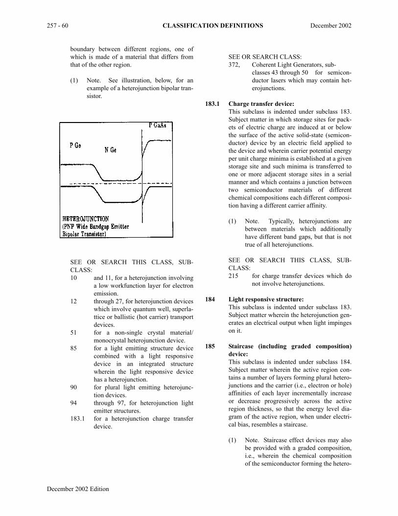
257 - 60 CLASSIFICATION DEFINITIONS December 2002
boundary between different regions, one ofwhich is made of a material that differs fromthat of the other region.
(1) Note. See illustration, below, for anexample of a heterojunction bipolar tran-sistor.
SEE OR SEARCH THIS CLASS, SUB-CLASS:10 and 11, for a heterojunction involving
a low workfunction layer for electronemission.
12 through 27, for heterojunction deviceswhich involve quantum well, superla-ttice or ballistic (hot carrier) transportdevices.
51 for a non-single crystal material/monocrystal heterojunction device.
85 for a light emitting structure devicecombined with a light responsivedevice in an integrated structurewherein the light responsive devicehas a heterojunction.
90 for plural light emitting heterojunc-tion devices.
94 through 97, for heterojunction lightemitter structures.
183.1 for a heterojunction charge transferdevice.
SEE OR SEARCH CLASS:372, Coherent Light Generators, sub-
classes 43 through 50 for semicon-ductor lasers which may contain het-erojunctions.
183.1 Charge transfer device:This subclass is indented under subclass 183.Subject matter in which storage sites for pack-ets of electric charge are induced at or belowthe surface of the active solid-state (semicon-ductor) device by an electric field applied tothe device and wherein carrier potential energyper unit charge minima is established at a givenstorage site and such minima is transferred toone or more adjacent storage sites in a serialmanner and which contains a junction betweentwo semiconductor materials of differentchemical compositions each different composi-tion having a different carrier affinity.
(1) Note. Typically, heterojunctions arebetween materials which additionallyhave different band gaps, but that is nottrue of all heterojunctions.
SEE OR SEARCH THIS CLASS, SUB-CLASS:215 for charge transfer devices which do
not involve heterojunctions.
184 Light responsive structure:This subclass is indented under subclass 183.Subject matter wherein the heterojunction gen-erates an electrical output when light impingeson it.
185 Staircase (including graded composition)device:This subclass is indented under subclass 184.Subject matter wherein the active region con-tains a number of layers forming plural hetero-junctions and the carrier (i.e., electron or hole)affinities of each layer incrementally increaseor decrease progressively across the activeregion thickness, so that the energy level dia-gram of the active region, when under electri-cal bias, resembles a staircase.
(1) Note. Staircase effect devices may alsobe provided with a graded composition,i.e., wherein the chemical compositionof the semiconductor forming the hetero-
1December 2002 Edition

December 2002 CLASSIFICATION DEFINITIONS 257 - 61
junction varies in a direction either per-pendicular or parallel to the junction.
(2) Note. See illustration, below, for anexample of a staircase bandgap.
186 Avalanche photodetection structure:This subclass is indented under subclass 184.Subject matter wherein carriers generated inthe active region of the device in response tolight incident thereupon, achieve enoughkinetic energy to knock further carriers fromthe crystalline lattice of the active region pro-ducing an avalanche or snowball increase inoperating current level.
(1) Note. Avalanche photodetector devicesmay have bipolar transistor structure,i.e., wherein the heterojunction devicehas three terminals - an emitter, a collec-tor and a base, the operating currentcomprising both positive and negativeelectrical charges.
187 Having transistor structure:This subclass is indented under subclass 184.Subject matter wherein the light responsiveheterojunction device has three terminals - anemitter, collector, and a base; a source, drain,and gate; or a hybrid combination of each,which can provide gain or can be used as aswitch.
188 Having narrow energy band gap (<<1eV)layer (e.g., PbSnTe, HgCdTe, etc.):This subclass is indented under subclass 184.Subject matter wherein the light responsivedevice contains a narrow energy band gap(<<1eV) layer (e.g., PbSnTe or HgCdTe).
189 Layer is a group III-V semiconductor com-pound:This subclass is indented under subclass 188.Subject matter wherein the narrow energy bandgap layer is a semiconductor compound madeof one element taken from periodic table groupIII elements and another element taken fromperiodic table group V elements.
190 With lattice constant mismatch (e.g., withbuffer layer to accommodate mismatch):This subclass is indented under subclass 183.Subject matter wherein at least one of the mate-rials that form the heterojunction has a crystal-line lattice constant which is made to differfrom the lattice constant of the other materialwhich forms the heterojunction.
(1) Note. Typically, lattice mismatches aresought to be avoided. However, some-times they are desired, as for example,when the resulting strain favorablyaffects the properties of the strainedsemiconductor.
(2) Note. A buffer layer may be provided toaccommodate a lattice mismatch, i.e., alayer of material which mechanicallyseparates the layers which have differentlattice constants.
SEE OR SEARCH THIS CLASS, SUB-CLASS:18 for strained layer heterojunctions in a
superlattice.
191 Having graded composition:This subclass is indented under subclass 183.Subject matter wherein the chemical composi-tion of the semiconductor forming the hetero-junction varies continuously in a directioneither perpendicular or parallel to the junction.
December 2002 Edition

257 - 62 CLASSIFICATION DEFINITIONS December 2002
192 Field effect transistor:This subclass is indented under subclass 183.Subject matter wherein the heterojunction ispart of a field effect transistor, i.e., wherein thecurrent through the active heterojunction iscontrolled by a voltage applied between gateand source terminals of the device.
194 Doping on side of heterojunction with lowercarrier affinity (e.g., high electron mobilitytransistor (HEMT)):This subclass is indented under subclass 192.Subject matter wherein the heterojunction fieldeffect transistor has impurity dopant on the sideof the heterojunction with lower affinity for thecharge carriers (holes or electrons) supplied bythe dopant, so that the charge carriers spill overthe heterojunction into the side with higher car-rier affinity.
(1) Note. Typically, the spilled over chargecarriers constitute the conductive chan-nel connecting the source and drain elec-trodes.
(2) Note. Such devices may be providedwith a channel layer of semiconductormaterial other than group III-V com-pound semiconductor (e.g., IV-VI com-pound semiconductor, germaniumsemiconductor, etc.).
SEE OR SEARCH THIS CLASS, SUB-CLASS:12 through 27, for other closely related
quantum well and ballistic transportfield effect devices.
195 Combined with diverse type device:This subclass is indented under subclass 194.Subject matter wherein the heterojunction fieldeffect transistor with impurity dopant on theside of the heterojunction with lower affinityfor the charge carriers supplied by the dopant iscombined with another electronic device.
(1) Note. Typical diverse devises includecomplementary field effect transistors,i.e., a field effect transistor of oppositeconductivity type to the heterojunctionfield effect transistor; and field effecttransistors of different threshold voltages
(e.g., enhancement and depletionHEMTs in same integrated circuit).
196 Both semiconductors of the heterojunctionare the same conductivity type (i.e., either nor p):This subclass is indented under subclass 183.Subject matter wherein the semiconductormaterials which define the heterojunction areof the same conductivity type (e.g., both p orboth n).
197 Bipolar transistor:This subclass is indented under subclass 183.Subject matter wherein the heterojunction ispart of a bipolar transistor, i.e., a transistorstructure whose working current passesthrough semiconductor material of both polari-ties (p and n) which form a heterojunction por-tion of the transistor.
SEE OR SEARCH CLASS:438, Semiconductor Device Manufactur-
ing: Process, particularly subclasses312+ for methods of forming a hetero-junction bipolar transistor.
198 Wide band gap emitter:This subclass is indented under subclass 197.Subject matter wherein the bipolar transistorwith an active heterojunction region involves acharge carrier emitter region made of a semi-conductor material having an energy gapbetween its conduction and valence bandswhich is greater than the energy gap of the baseregion forming a heterojunction therewith.
199 Avalanche diode (e.g., so-called “Zener”diode having breakdown voltage greaterthan 6 volts, including heterojunctionIMPATT type microwave diodes):This subclass is indented under subclass 183.Subject matter wherein the heterojunctiondevice is a diode in which conduction underreverse bias conditions is caused by avalanchebreakdown at an applied voltage greater than 6volts.
(1) Note. One example of such a device is amicrowave transit time device (e.g.,IMPATT diode).
1December 2002 Edition

December 2002 CLASSIFICATION DEFINITIONS 257 - 63
SEE OR SEARCH THIS CLASS, SUB-CLASS:481 for a Schottky barrier avalanche
diode.551 for an avalanche diode used as a volt-
age reference element combined withpn junction isolation means in an inte-grated circuit.
603 through 606, for avalanche diodes notclassified above those subclasses inthis schedule, i.e., not involving a het-erojunction in a non-charge transferdevice, or a Schottky barrier, or oneused as a voltage reference elementwith pn junction isolation means in anintegrated circuit.
SEE OR SEARCH CLASS:331, Oscillators, subclasses 107+ for solid-
state active element oscillators.
200 Heterojunction formed between semicon-ductor materials which differ in that theybelong to different periodic table groups(e.g., Ge (group IV) - GaAs (group III-V) orInP (group III-V) - CdTe (group II-VI)):This subclass is indented under subclass 183.Subject matter wherein the heterojunction isformed between semiconductor materialswhich differ in that they belong to differentperiodic table groups (e.g., Ge (group IV) -GaAs (group III-V) or InP (group III-V) -CdTe (group II-VI)).
201 Between different group IV-VI or II-VI orIII-V compounds other than GaAs/GaAlAs:This subclass is indented under subclass 183.Subject matter wherein the heterojunctionforms a boundary between different group IV-VI or group II-VI or group III-V compoundsother than GaAs/GaAlAs.
202 GATE ARRAYS:This subclass is indented under the class defini-tion. Subject matter comprising a repeatinggeometric arrangement of individual structuralunits of solid-state devices, the solid-statedevices of each individual structural unit beingconnectable into various different types oflogic circuits in one integrated, monolithicchip.
(1) Note. The significant distinctionbetween a “gate array” and other arraysof active solid state devices, such asread-only memories (ROMs), and pro-grammable logic arrays (PLAs), is thatthe solid-state devices of each individualstructural of a “gate array” can be con-nected into various different types oflogic circuits, whereas in a ROM orPLA, each of the individual structuralunits is configured so that they must beconnected into the same type of logiccircuit (e.g., wherein all individual struc-tural units are connected as NOR gates).
SEE OR SEARCH CLASS:438, Semiconductor Device Manufactur-
ing: Process, particularly subclasses128+ for methods of forming an arrayof devices upon a semiconductor sub-strate and selectively interconnectingthe same.
203 With particular chip input/output means:This subclass is indented under subclass 202.Subject matter wherein the gate array inte-grated circuit is provided with specific meansto input and output electrical signals to operatethe device.
(1) Note. Examples of particular chip input/output means include (a) interface cir-cuits, i.e., circuits that connect the chipto another device or to a circuit andwhich produces necessary current andvoltage characteristics for the intercon-nected devices and circuits to functionproperly, with particular active solid-state devices used in the interface cir-cuits; (b) structure permitting electricalinterconnection to either receive an inputsignal or to output an output signal; or(c) specific bonding pad or electrodeconfigurations (i.e., wherein the input/output means includes a particular elec-trically conductive surface to whichelectrical interconnecting element (e.g.,electrical leads) can be connected, or hasa specified electrode configuration suchas a power supply bus for the input/out-put means separate from those used topower the gate array devices.
December 2002 Edition

257 - 64 CLASSIFICATION DEFINITIONS December 2002
204 Having specific type of active device (e.g.,CMOS):This subclass is indented under subclass 202.Subject matter wherein the gate array isadapted to use a particular type of solid-stateelectronic device, e.g., complementary metaloxide semiconductor device (CMOS).
205 With bipolar transistors or with FETs ofonly one channel conductivity type (e.g.,enhancement-depletion FETs):This subclass is indented under subclass 202.Subject matter wherein the specific type ofactive device comprises bipolar transistors orFETs of only one channel conductivity type(i.e, field effect transistors that can be used inthe enhancement or depletion mode of opera-tion, e.g., IGFETS).
206 Particular layout of complementary FETswith regard to each other:This subclass is indented under subclass 204.Subject matter wherein the CMOS deviceincludes a plurality of CMOS field effect tran-sistors specifically arranged with regard toeach other.
207 With particular power supply distributionmeans:This subclass is indented under subclass 202.Subject matter wherein the gate array is pro-vided with specific means to provide electricalpower to the array.
208 With particular signal path connections:This subclass is indented under subclass 202.Subject matter wherein the gate array is pro-vided with specific signal path connections.
209 Programmable signal paths (e.g., with fuseelements, laser programmable, etc):This subclass is indented under subclass 208.Subject matter wherein the gate array is pro-vided with means (e.g., fuse elements or laserbeam irradiation) to program the selection ofsignal paths in the array.
210 With wiring channel area:This subclass is indented under subclass 208.Subject matter wherein the signal paths in thearray are located in an area separate from theactive devices forming the elements of thearray.
211 Multi-level metallization:This subclass is indented under subclass 208.Subject matter wherein the particular signalpath connections include more than one layerof conductive metal deposited on a substrate.
(1) Note. The multilayer metallization mayinclude a layer of material made up ofsilicon in polycrystalline form or a sili-cide compound.
212 CONDUCTIVITY MODULATIONDEVICE (E.G., UNIJUNCTION TRANSIS-TOR, DOUBLE-BASE DIODE, CONDUC-TIVITY-MODULATED TRANSISTOR):This subclass is indented under the class defini-tion. Subject matter wherein the active solid-state device has a high resistivity semiconduc-tor region of one conductivity type having aregion of opposite conductivity type forming apn junction with a central portion of the highresistivity layer, with structural means pro-vided to forward bias the pn junction to injectminority carriers into the high resistivity regionto increase its conductivity through conductiv-ity modulation.
SEE OR SEARCH CLASS:327, Miscellaneous Active Electrical Non-
linear Devices, Circuits, and Systems, subclasses 397 and 402 for a delaycontrolled switch using a unijunctiontransistor and having a variable orfixed delay respectively; subclasses438+ for gating circuits utilizing aunijunction transistor, and subclass569 for a miscellaneous circuit whichutilizes a unijunction transistor.
361, Electricity: Electrical Systems andDevices, subclass 91.3 for overvolt-age protection with time delay, andsubclass 198 for time delay with uni-junction devices.
388, Electricity: Motor Control Systems, subclass 919 for unijunction transistorcircuit trigger control means.
213 FIELD EFFECT DEVICE:This subclass is indented under the class defini-tion. Subject matter comprising a field effecttransistor, in which the density of electricalcharge (electrons or holes) in a semiconductorregion is controlled by a voltage applied to an
1December 2002 Edition

December 2002 CLASSIFICATION DEFINITIONS 257 - 65
adjacent region or electrode which in operationis prevented from conducting direct electricalcurrent to or from the semiconductor region byan insulator or barrier region.
(1) Note. The conduction of current in afield effect device is along a path called achannel.
(2) Note. See Illustration, below, for varioustypes of field effect devices.
SEE OR SEARCH CLASS:331, Oscillators, subclasses 116 and 117
for field effect transistor oscillatoractive elements.
341, Coded Data Generation or Conver-sion, subclass 136 for analog to orfrom digital conversion devices with afield effect transistor.
214 Charge injection device:This subclass is indented under subclass 213.Subject matter wherein the field effect deviceis a device in which storage sites for packets ofelectric charge are induced at or below the sur-face of the active solid-state (semiconductor)device by an electric field applied to the deviceand wherein carrier potential energy per unitcharge minima are established at a given stor-
age site and such charge packets are injectedinto the device substrate or into a data bus.
(1) Note. This type device differs from acharge transfer device in that, in the lat-ter, charge is transferred to adjacentcharge storage sites in a serial mannerwhereas in the former, the charge isinjected in a non-serial manner to thedevice substrate or a data bus.
215 Charge transfer device:This subclass is indented under subclass 213.Subject matter in which storage sites for pack-ets of electric charge are induced at or belowthe surface of the active solid-state (semicon-ductor) device by an electric field applied tothe device and wherein carrier potential energyper unit charge minima are established at agiven storage site and such minima are trans-ferred to one or more adjacent storage sites in aserial manner.
SEE OR SEARCH THIS CLASS, SUB-CLASS:183.1 for heterojunction type charge transfer
devices.
SEE OR SEARCH CLASS:438, Semiconductor Device Manufactur-
ing: Process, subclass 60 for meth-ods of making a photo-responsivesemiconductor integrated circuit hav-ing a charge transfer device combinedwith another electrical device, sub-classes 75+ for methods of making aphotoresponsive charge transferdevice, and subclasses 144+ for meth-ods of making a charge transferdevice.
216 Majority signal carrier (e.g., buried or bulkchannel, or peristaltic):This subclass is indented under subclass 215.Subject matter wherein the transfer is bymajority carriers of the semiconductor mate-rial, i.e., by electrons in n-type semiconductormaterial, and is by holes in p-type semiconduc-tor material.
December 2002 Edition
257 - 66 CLASSIFICATION DEFINITIONS December 2002
217 Having a conductive means in direct contactwith channel (e.g., non-insulated gate):This subclass is indented under subclass 216.Subject matter wherein an electrical conductor(e.g., electrode) directly contacts the channelregion of the charge transfer device (e.g., anon-insulated gate (control) electrode).
(1) Note. The conductive means in directcontact with the channel may be directlyconnected to the substrate.
(2) Note. The conductive means in directcontact with the channel may be made ofmetal, forming a Schottky contact withthe semiconductor channel material, i.e.,a metal-semiconductor junction.
218 High resistivity channel (e.g., accumulationmode) or surface channel (e.g., transfer ofsignal charge occurs at the surface of thesemiconductor) or minority carriers at input(i.e., surface channel input):This subclass is indented under subclass 216.Subject matter wherein the majority signal car-rier charge transfer device has a channel madeof relatively high electrical resistivity material,or where the transfer of signal charge takesplace at the surface of the semiconductor, orwhere minority charge carriers are input into asurface channel, but majority carriers are inputinto the bulk or buried channel portion of thedevice.
219 Impurity concentration variation:This subclass is indented under subclass 216.Subject matter wherein the majority signal car-rier charge transfer device contains impuritydopant ions which vary in terms of concentra-tion in all or part of the channel of the device.
(1) Note. The impurity dopant ion concen-tration may vary across the channel andchannel substrate interface.
220 Vertically within channel (e.g., profiled):This subclass is indented under subclass 219.Subject matter wherein the impurity dopant ionconcentration in the channel of the device var-ies across the channel in a direction perpendic-ular to a main surface of the device, regardlessof the orientation of the channel (e.g., parallel
or perpendicular to a main surface of thedevice).
221 Along the length of the channel (e.g., dopingvariations for transfer directionality):This subclass is indented under subclass 219.Subject matter wherein the impurity dopant ionconcentration in the channel of the device var-ies along the length of the channel, whether thechannel is horizontally or vertically oriented.
222 Responsive to non-electrical external signal(e.g., imager):This subclass is indented under subclass 216.Subject matter wherein the majority signal car-rier charge transfer device transfers chargefrom one charge storage device to another inresponse to a non-electric signal (e.g., light,pressure, etc.).
223 Having structure to improve output signal(e.g., antiblooming drain):This subclass is indented under subclass 222.Subject matter wherein the non-external signalresponsive device includes structural means,e.g., a drain element which reduces or elimi-nates optical blooming to improve the signalgenerated by the device in response to the non-electrical input signal.
224 Channel confinement:This subclass is indented under subclass 216.Subject matter wherein the majority carriercharge transfer device has means to restrict thedimensions of the thin semiconductor conduc-tive path region (charge transfer channel)between the source and drain of the device.
225 Non-electrical input responsive (e.g., lightresponsive imager, input programmed bysize of storage sites for use as a read-onlymemory, etc.):This subclass is indented under subclass 215.Subject matter wherein the means that createscharge to be transferred is non-electrical (e.g.,light).
226 Sensor element and charge transfer deviceare of different materials or on differentsubstrates (e.g., “hybrid”):This subclass is indented under subclass 225.Subject matter wherein charge carriers gener-ated in response to the non-electrical input aregenerated in material which is different than, or
1December 2002 Edition

December 2002 CLASSIFICATION DEFINITIONS 257 - 67
is located on a different substrate than, thesemiconductor material that contains thecharge carrier storage sites.
227 With specified dopant (e.g., photoionizable,“extrinsic” detectors for infrared):This subclass is indented under subclass 225.Subject matter wherein the non-electricalresponsive device contains specific impuritydopants.
228 Light responsive, back illuminated:This subclass is indented under subclass 225.Subject matter wherein the non-electrical inputresponsive device has two major opposed sur-faces, the channel containing the charge carrierstorage sites being at or below one surface, andwherein the device is responsive to light whichis incident on the other major surface.
229 Having structure to improve output signal(e.g., exposure control structure):This subclass is indented under subclass 225.Subject matter wherein the non-electrical inputresponsive device contains structural means toimprove the electrical signal it generates inresponse to the non-electrical input signal.
(1) Note. The structural means to improvethe output signal may control the amountof charge generated by light incident onthe device which is transferred as outputsignal charge.
230 With blooming suppression structure:This subclass is indented under subclass 229.Subject matter wherein the structural means toimprove the output signal prevents spill over ofa large amount of signal charge generated at astorage site which receives a non-electricalinput signal of very high intensity to adjacentstorage sites.
(1) Note. The antiblooming suppressionstructure may include a drain structurefor removing charge from storage sites.
(2) Note. The antiblooming drain structuremay be located in the device beneathstorage sites rather than on its surface.
231 2-dimensional area architecture:This subclass is indented under subclass 225.Subject matter wherein the device has a plural-ity of non-electrical input responsive meansspread out over a two dimensional area, e.g., amatrix or array of such means.
(1) Note. One 2-dimensional architecturearea may be provided for light imagingelements and a separate 2-dimensionalarchitecture area may be provided forelectrical signal storage elements.
(2) Note. The imaging element sites mayalso be charge transfer storage sites (e.g.,frame transfer imaging device).
232 Having alternating strips of sensor struc-tures and register structures (e.g., interlineimager):This subclass is indented under subclass 231.Subject matter wherein the 2-dimensional areaarchitecture has alternate strips of sensor struc-tures and charge transfer channels.
233 Sensors not overlaid by electrode (e.g., pho-todiodes):This subclass is indented under subclass 232.Subject matter wherein the light responsivesensor elements do not have an electrode over-lying them.
234 Single strip of sensors (e.g., linear imager):This subclass is indented under subclass 225.Subject matter wherein the non-electrical inputresponsive device is in the form of a line ofindividual sensors.
(1) Note. The single strip of sensors may becombined with a structure forming read-out registers, i.e., short term storagedevices for accumulating charge packetsgenerated by the sensors and for trans-ferring charge packets to an amplifier oroutput device, and wherein the sensorsare placed adjacent to the readout regis-ter structure.
(2) Note. The device may have plural read-out register structures.
December 2002 Edition

257 - 68 CLASSIFICATION DEFINITIONS December 2002
235 Electrical input:This subclass is indented under subclass 215.Subject matter wherein the input to the chargetransfer device to create the charge to be trans-ferred is an electrical signal.
236 Signal applied to field effect electrode:This subclass is indented under subclass 235.Subject matter wherein means is provided toapply an electrical signal to an electrode whichhas an electrical potential barrier between theelectrode and the semiconductor material of thedevice (e.g., a MOS dielectric or Schottky con-tact or reverse-biased junction), as contrastedwith an ohmic electrical contact to the semi-conductor.
237 Charge-presetting/linear input type (e.g., filland spill):This subclass is indented under subclass 236.Subject matter wherein means is provided forthe input signal to form a potential well, over-fill it, drain away the excess charge and inputthe preset charge in the potential well into thechannel.
238 Input signal responsive to signal charge incharge transfer device (e.g., regeneration orfeedback):This subclass is indented under subclass 235.Subject matter wherein means is provided totake charge from the output of a charge transferdevice and put it back into the input electrodethereof or into the input electrode of a secondcharge transfer device.
239 Signal charge detection type (e.g., floatingdiffusion or floating gate non-destructiveoutput):This subclass is indented under subclass 215.Subject matter wherein means is provided todetect the amount of charge being transferredin the device.
(1) Note. The charge being transferred maybe measured without destroying thecharge, i.e., the charge packet remainsintact.
(2) Note. The charge transfer device mayhave a region diffused with impurity ionsnot electrically connected to ground todetect the magnitude of charge being
transferred in the device and to output asignal proportional to that sensed charge.This is known as a floating diffusion out-put device. One example of such adevice is a floating diffusion amplifier(FDA).
(3) Note. The charge transfer device mayhave a control electrode not electricallyconnected to ground to detect the magni-tude of charge being transferred in thedevice and to output a signal propor-tional to that sensed charge. This typedevice is known as a floating gate outputdevice. One example of such a device isa floating gate amplifier (FGA). Deviceswith plural floating gate outputs includedistributed floating gate amplifiers(DFGA).
240 Changing width or direction of channel(e.g., meandering channel):This subclass is indented under subclass 215.Subject matter wherein the charge transfer pathregion changes its width or direction through-out all or part of the distance from source todrain electrode.
241 Multiple channels (e.g., converging ordiverging or parallel channels):This subclass is indented under subclass 215.Subject matter wherein the charge transferdevice contains more than one channel forcharge transfer path.
(1) Note. The channels may converge ordiverge, i.e., they are not parallel to eachother, but change direction either towardor away from each other along theirlength.
(2) Note. In such devices, the charge trans-fer path may lie in two different (e.g.,orthogonal) directions.
(3) Note. The device may include two ormore parallel channels (e.g., serial- par-allel-serial) wherein the charge transfertakes place in different directions, butthe device includes charge transfer pathsthat are parallel to each other.
1December 2002 Edition

December 2002 CLASSIFICATION DEFINITIONS 257 - 69
242 Vertical charge transfer:This subclass is indented under subclass 215.Subject matter wherein the charge transferdevice is provided with structure for verticalcharge transfer perpendicular to a main devicesurface.
243 Channel confinement:This subclass is indented under subclass 215.Subject matter containing means (e.g., pn junc-tions or dielectric layers) to restrict the bound-aries of the charge transfer path through thedevice.
(1) Note. Typical channel confinementmeans include use of (a) an electricallyinsulating medium; (b) a layer of siliconpolymer material (polysilicon) used toreduce electric field interaction withcharge to be transferred via the channel;or (c) an impurity ion located in thedevice substrate, i.e., in the material onwhich the device is fabricated (e.g., animplanted channel stop).
244 Comprising a groove:This subclass is indented under subclass 215.Subject matter wherein a surface of the deviceincludes an elongated indentation.
(1) Note. The location of the groove relativeto the charge storage sites of the deviceis deliberately not specified in this defi-nition.
245 Structure for applying electric field intodevice (e.g., resistive electrode, acoustictraveling wave in channel):This subclass is indented under subclass 215.Subject matter including structure (e.g., elec-trodes) for applying electrical energy into thedevice.
(1) Note. Structure for applying electricalenergy into the device is typically anelectrode with a relatively high electricalresistance value.
246 Phase structure (e.g., doping variations toprovide asymmetry for 2-phase operation;
more than four phases or “electrode perbit”):This subclass is indented under subclass 245.Subject matter including a plurality of gateregions or doping variation regions to permitunidirectional charge packet transfer by sym-metrical or unsymmetrically phased electricalcontrol signals applied to the device gate orgates.
(1) Note. The phase structure may be multi-phase (e.g., 3-phase or 4-phase), i.e.,with three sets or four sets of electrodes,respectively.
(2) Note. Search subclass 249, below, for 2-phase structure devices.
(3) Note. Means may also be provided togenerate a traveling wave of non-electri-cal energy (e.g., acoustic energy) in thedevice.
247 Uniphase or virtual phase structure:This subclass is indented under subclass 246.Subject matter wherein the device has one setof gates (control electrodes) or virtual phasestructure.
248 2-phase:This subclass is indented under subclass 246.Subject matter wherein the device has two setsof gate electrodes.
249 Electrode structures or materials:This subclass is indented under subclass 245.Subject matter wherein the charge transferdevice is provided with specified electrodestructures or materials to apply electric fieldinto the device.
250 Plural gate levels:This subclass is indented under subclass 249.Subject matter wherein the electrode structuresinclude more than one level of gate electrodesrelative to a main surface of the device.
251 Substantially incomplete signal chargetransfer (e.g., bucket brigade):This subclass is indented under subclass 215.Subject matter wherein the charge transferredis less than the entire charge stored in the stor-age site from which it originates.
December 2002 Edition

257 - 70 CLASSIFICATION DEFINITIONS December 2002
252 Responsive to non-optical, non-electricalsignal:This subclass is indented under subclass 213.Subject matter which produces an electricaloutput in response to an input which is otherthan optical or electrical.
253 Chemical (e.g., ISFET, CHEMFET):This subclass is indented under subclass 252.Subject matter wherein the input is a chemicalreaction or the presence of a particular chemi-cal in close proximity to the field effect device.
254 Physical deformation (e.g., strain sensor,acoustic wave detector):This subclass is indented under subclass 252.Subject matter wherein the input is a physicaldeformation.
SEE OR SEARCH THIS CLASS, SUB-CLASS:416 for acoustic wave responsive devices,
generally.
255 With current flow along specified crystalaxis (e.g., axis of maximum carrier mobil-ity):This subclass is indented under subclass 213.Subject matter wherein the field effect deviceemploys current flow along a specified crystalaxis, such as a (100) axis or a (311) axis.
256 Junction field effect transistor (unipolartransistor):This subclass is indented under subclass 213.Subject matter wherein the field effect deviceis a junction field effect transistor, i.e., inwhich current flow through a thin channel ofsemiconductor material is controlled by anelectric field applied to a control region or elec-trode in rectifying contact (i.e., a pn junctionor Schottky barrier junction) with the semicon-ductor material of the channel, so that thedepletion region extending into the channelfrom the rectifying contact reduces the thick-ness of the undepleted portion of the channel toreduce the current flow through the channel.
SEE OR SEARCH CLASS:438, Semiconductor Device Manufactur-
ing: Process, particularly subclasses167+ for methods of forming aSchottky gate field effect device and
subclasses 186+ for methods of form-ing a junction gate field effect device.
257 Light responsive or combined with lightresponsive device:This subclass is indented under subclass 256.Subject matter wherein the JFET generates anelectrical signal when light energy is incidentupon it or is combined with a light responsivedevice.
258 In imaging array:This subclass is indented under subclass 257.Subject matter wherein a plurality of lightresponsive JFETs or JFETs combined with alight responsive device are in the form of a oneor two dimensional array (e.g., line or areaarray) for forming an image of an object, lightfrom which is incident upon the array.
259 Elongated active region acts as transmissionline or distributed active element (e.g.,“transmission line” field effect transistor):This subclass is indented under subclass 256.Subject matter including at least one elongatedactive region (source, gate, or drain) whichtransmits or distributes charge carriers.
(1) Note. When the impedance of an ele-ment at the operating frequency is dueprimarily to the parameters of the ele-ment itself, and in considering the induc-tance, capacitance, and resistance of theelement they must be considered asmixed together and spread out along theelement rather than being considered asseparate discrete lumps or componentsas in the case of simple series and paral-lel circuits, the element may be said tohave distributed parameters.
SEE OR SEARCH CLASS:333, Wave Transmission Lines and Net-
works, appropriate subclasses fortransmission lines or distributed ele-ments, per se.
438, Semiconductor Device Manufactur-ing: Process, particularly subclasses167+ for methods of forming aSchottky gate field effect device andsubclasses 186+ for methods of form-ing a junction gate field effect device.
1December 2002 Edition
December 2002 CLASSIFICATION DEFINITIONS 257 - 71
260 Same channel controlled by both junctionand insulated gate electrodes, or by bothSchottky barrier and pn junction gates (e.g.,“taper isolated” memory cell):This subclass is indented under subclass 256.Subject matter including plural gate electrodesor regions, at least one of which is isolatedfrom the channel by a rectifying junction and atleast another of which is isolated from thechannel by an insulating layer therebetween, orwherein one rectifying junction may be ametal-to-semiconductor (Schottky) type andthe other a pn junction.
(1) Note. In such devices, the junction gateregion may be free of direct electricalconnection (e.g., “taper isolated” mem-ory cell), i.e., wherein the JFET has atleast one gate electrode region which isisolated from the channel by a rectifyingjunction and is not directly providedwith an electrical connection or terminal.
261 Junction gate region free of direct electricalconnection (e.g., floating junction gate mem-ory cell structure):This subclass is indented under subclass 256.Subject matter including at least one gate elec-trode region which is isolated from the channelby a rectifying junction and is not directly pro-vided with an electrical connection or terminal.
(1) Note. This type of gate is a floatingjunction gate, as contrasted with a float-ing insulated gate.
(2) Note. See this class, subclass 315, forfloating insulated gate field effectdevices.
(3) Note. The floating gate region maycapacitively store electrical charge andbe used as a memory element.
262 Combined with insulated gate field effecttransistor (IGFET):This subclass is indented under subclass 256.Subject matter including a field effect transis-tor having a gate (control) electrode which iselectrically insulated from the channel andother electrodes of the transistor.
(1) Note. The combined JFET and IGFETmay be electrically connected so that thesource or drain electrode of one FET isconnected to the gate electrode of theother FET.
263 Vertical controlled current path:This subclass is indented under subclass 256.Subject matter wherein the operating current ofthe JFET has a path perpendicular to a mainsurface of the JFET and is controlled by thegate electrode of the device.
264 Enhancement mode or with high resistivity
channel (e.g., doping of 1015cm-3 or less):This subclass is indented under subclass 263.Subject matter wherein an increase in the mag-nitude of the gate bias voltage increases theoperating current, only leakage current flowswhen the gate voltage is zero, and conductiondoes not begin until the gate voltage reaches athreshold value; or the JFET has a channelmade of relatively high electrical resistivity,
e.g., due to doping with impurity ions of 1015
cm-3 or less.
265 In integrated circuit:This subclass is indented under subclass 263.Subject matter in a single monolithic semicon-ductor chip with other active and/or passivedevices.
266 With multiple parallel current paths (e.g.,grid gate):This subclass is indented under subclass 263.Subject matter having plural paths for operat-ing current flow, each of which is parallel withthe other paths (e.g., having a gate electrode inthe form of a matrix or grid).
267 With Schottky barrier gate:This subclass is indented under subclass 266.Subject matter including a gate which isformed by a metal to semiconductor rectifyingjunction.
268 Enhancement mode:This subclass is indented under subclass 256.Subject matter wherein an increase in the mag-nitude of the gate bias voltage increases theoperating current, only leakage current flowswhen the gate voltage is zero, and conduction
December 2002 Edition

257 - 72 CLASSIFICATION DEFINITIONS December 2002
does not begin until the gate voltage reaches athreshold value.
269 With means to adjust barrier height (e.g.,doping profile):This subclass is indented under subclass 268.Subject matter including means to adjust theelectronic height of the Schottky barrier gatejunction, e.g., a profiled impurity dopant con-centration.
270 Plural, separately connected, gates controlsame channel region:This subclass is indented under subclass 256.Subject matter including more than one gateregion or portion to control the same channelregion, the regions being provided with sepa-rate electrical connections.
271 Load element or constant current source(e.g., with source to gate connection):This subclass is indented under subclass 256.Subject matter structured to function as anelectrical load element or a source of constantcurrent, e.g., with a source to gate electricalconnection.
272 Junction field effect transistor in integratedcircuit:This subclass is indented under subclass 256.Subject matter located in a single monolithicsemiconductor chip with other active and/orpassive devices.
273 With bipolar device:This subclass is indented under subclass 272.Subject matter located in an integrated circuitwith a device which operates using both posi-tive and negative charge carriers.
(1) Note. An active solid-state electronicdevice that contains both bipolar andfield effect transistors may be referred toas a BI-FET device.
274 Complementary junction field effect transis-tors:This subclass is indented under subclass 272.Subject matter which is located in and inte-grated with an opposite conductivity typeJFET, i.e., an N channel JFET together with a Pchannel JFET.
275 Microwave integrated circuit (e.g.,microstrip type):This subclass is indented under subclass 272.Subject matter structured to operate at micro-wave frequencies in an integrated circuit con-taining microwave components (e.g.,microstrip transmission lines).
276 With contact or heat sink extending throughhole in semiconductor substrate, or withelectrode suspended over substrate (e.g., airbridge):This subclass is indented under subclass 275.Subject matter containing a hole in the semi-conductor substrate and an electrical contact ora heat dissipation means extending through thehole.
SEE OR SEARCH THIS CLASS, SUB-CLASS:522 for integrated circuit devices employ-
ing air isolation.
277 With capacitive or inductive elements:This subclass is indented under subclass 275.Subject matter having passive elements withelectrical inductance or capacitance.
278 With devices vertically spaced in differentlayers of semiconductor material (e.g., “3-dimensional” integrated circuit):Subject matter under 272 wherein the JFETand other active and/or passive devices in thatchip are located in mutually perpendicularplanes in different layers of semiconductordevice material.
279 Pn junction gate in compound semiconduc-tor material (e.g., GaAs):This subclass is indented under subclass 256.Subject matter including a pn junction gateformed in a semiconductor material that is acompound, e.g., GaAs, as contrasted to an ele-mental semiconductor such as silicon or ger-manium.
280 With Schottky gate:This subclass is indented under subclass 256.Subject matter including a metal to semicon-ductor rectifying (i.e., Schottky barrier) gateelectrode.
1December 2002 Edition

December 2002 CLASSIFICATION DEFINITIONS 257 - 73
(1) Note. A Schottky barrier gate JFET isreferred to commonly as a MESFET(MEtal-Semiconductor field effect tran-sistor).
281 Schottky gate to silicon semiconductor:This subclass is indented under subclass 280.Subject matter wherein the semiconductormaterial contacting the gate electrode materialis made of silicon.
282 Gate closely aligned to source region:This subclass is indented under subclass 280.Subject matter wherein the gate region isclosely aligned with the source region.
SEE OR SEARCH THIS CLASS, SUB-CLASS:332 346, 387, and 797, for other self-
aligned gate devices.
283 With groove or overhang for alignment:This subclass is indented under subclass 282.Subject matter wherein the device has a grooveor overhang for alignment of the gate andsource regions.
284 Schottky gate in groove:This subclass is indented under subclass 280.Subject matter wherein the MESFET has agroove in at least one of its surfaces and theSchottky gate is located therein.
285 With profiled channel dopant concentrationor profiled gate region dopant concentration(e.g., maximum dopant concentration belowsurface):This subclass is indented under subclass 256.Subject matter wherein the JFET has a variableimpurity atom dopant concentration in thechannel or gate region, e.g., wherein the maxi-mum dopant concentration is located below thesurface of the device, in either the channel orgate region.
286 With non-uniform channel thickness orwidth:This subclass is indented under subclass 256.Subject matter wherein the channel has a non-uniform width or thickness (which lies in aplane perpendicular to both the channel lengthand width).
(1) Note. Channel length is measured alonga line connecting the source and drain,while channel width is measured perpen-dicular to the length. Both length andwidth lie in a plane, parallel to the devicesurface. See the illustration, below.
287 With multiple channels or channel segmentsconnected in parallel, or with channel muchwider than length between source and drain(e.g., power JFET):This subclass is indented under subclass 256.Subject matter including more than one chan-nel or channel segments/portions which areelectrically connected in parallel, or whereinthe device has a channel whose width is muchwider than the channel length, the channellength being the distance between the sourceand drain of the JFET.
SEE OR SEARCH THIS CLASS, SUB-CLASS:134+, for JFET devices, in general.504 for JFET type isolation.
288 Having insulated electrode (e.g., MOSFET,MOS diode):This subclass is indented under subclass 213.Subject matter including an electrode which iselectrically insulated from the active semicon-
December 2002 Edition

257 - 74 CLASSIFICATION DEFINITIONS December 2002
ductor region of the device (e.g., a metal oxidesemiconductor insulated electrode).
(1) Note. Typically the insulated electrodeis the control or gate electrode.
SEE OR SEARCH CLASS:438, Semiconductor Device Manufactur-
ing: Process, particularly subclasses197+ for methods of forming an insu-lated gate field effect device.
289 Significant semiconductor chemical com-pound in bulk crystal (e.g., GaAs):This subclass is indented under subclass 288.Subject matter wherein the insulated electrodefield effect device contains a significant semi-conductor chemical compound in a bulk (ascontrasted with thin film) crystal (e.g., GaAs).
SEE OR SEARCH THIS CLASS, SUB-CLASS:1+, for bulk effect devices.
290 Light responsive or combined with lightresponsive device:This subclass is indented under subclass 288.Subject matter which generates an electricalsignal when light is incident on it or is com-bined with a light responsive device.
291 Imaging array:This subclass is indented under subclass 290.Subject matter comprising a one or moredimensional array of light responsive deviceswhich generate an electronic image of lightfrom an object incident thereupon.
292 Photodiodes accessed by FETs:This subclass is indented under subclass 291.Subject matter comprising light responsivediodes electrically coupled to field effect tran-sistors.
293 Photoresistors accessed by FETs, or photo-detectors separate from FET chip:This subclass is indented under subclass 291.Subject matter comprising light responsiveresistors coupled to field effect transistors.
294 With shield, filter, or lens:This subclass is indented under subclass 291.Subject matter including means to shield thearray from unwanted light, to filter light inci-
dent on the array, or to refract light incident onthe array (e.g., to focus an image of an objecton the array).
295 With ferroelectric material layer:This subclass is indented under subclass 288.Subject matter including a layer of materialwhich exhibits a spontaneous dipole moment.
296 Insulated gate capacitor or insulated gatetransistor combined with capacitor (e.g.,dynamic memory cell):This subclass is indented under subclass 288.Subject matter wherein the device gate acts as acapacitor (i.e., wherein a positive potentialplaced on the gate electrode creates a negativecharge on the other side of the insulator in thesemiconductor material of the device, and viceversa) or the device is a transistor and it iscombined with a capacitor.
SEE OR SEARCH CLASS:438, Semiconductor Device Manufactur-
ing: Process, particularly subclasses239+ for methods of forming an insu-lated gate field effect transistor com-bined with a capacitor and subclasses386 through 399 for manufacture of acapacitors, per se, utilizing a semicon-ductor substrate.
297 With means for preventing charge leakagedue to minority carrier generation (e.g.,alpha generated soft error protection or“dark current” leakage protection):This subclass is indented under subclass 296.Subject matter wherein the device furtherincludes means (1) to prevent electrical chargein the capacitor or capacitive type insulatedgate region of the transistor to leak therefrom,or (2) to prevent excess leakage currents acrosspn junctions due to generation of minority car-riers in the device for example (a) alpha parti-cles incident on the device or (b) thermalgeneration of electron-hole pairs, or (c) minor-ity carriers injected into the semiconductorsubstrate by other devices in the same sub-strate.
(1) Note. Junctions across which excessleakage is sought to be prevented typi-cally include (a) the source or drain junc-tion of an insulated gate field effecttransistor or (b) a connecting BIT line of
1December 2002 Edition

December 2002 CLASSIFICATION DEFINITIONS 257 - 75
a memory array which is isolated by apn junction from a semiconductor sub-strate.
298 Capacitor for signal storage in combinationwith non-volatile storage means:This subclass is indented under subclass 296.Subject matter including a capacitor to store anelectrical signal in combination with chargestorage means that can retain the charge evenin the absence of operating power.
299 Structure configured for voltage converter(e.g., charge pump, substrate bias genera-tor):This subclass is indented under subclass 296.Subject matter including structure for use as avoltage converter (e.g., a device for changingAC to DC or vice versa, or for producing anegative DC voltage relative to a referencepotential from a positive DC voltage relative tothat reference potential).
300 Capacitor coupled to, or forms gate of, insu-lated gate field effect transistor (e.g., non-destructive readout dynamic memory cellstructure):This subclass is indented under subclass 296.Subject matter wherein the capacitor is electri-cally connected to or forms the gate of an insu-lated gate field effect transistor (IGFET), e.g., anon-destructive readout dynamic memory cellstructure in which the charge state of the capac-itor may be read out or determined by the con-duction state of the field effect transistor,without discharging the capacitor in the read-out process.
301 Capacitor in trench:This subclass is indented under subclass 296.Subject matter wherein the capacitor is locatedin a recess in the semiconductor substrate.
302 Vertical transistor:This subclass is indented under subclass 301.Subject matter combined with a vertical tran-sistor (i.e., one in which the operating currentflow is perpendicular to a main surface of thedevice).
303 Stacked capacitor:This subclass is indented under subclass 301.Subject matter wherein the trench capacitordevice contains a number of capacitor elec-
trode regions stacked vertically above eachother or wherein the capacitor and the transis-tor are located such that one overlies the other.
304 Storage node isolated by dielectric fromsemiconductor substrate:This subclass is indented under subclass 301.Subject matter including an electrode uponwhich the charge varies as an indication of thememory state of the device (e.g., memory cell),and wherein the electrode is electrically iso-lated by a dielectric material from the semicon-ductor substrate of the device.
305 With means to insulate adjacent storagenodes (e.g., channel stops or field oxide):This subclass is indented under subclass 301.Subject matter including means for electricallyinsulating an electrode upon which the chargevaries as an indication of the memory state ofthe device (e.g., a memory cell).
(1) Note. The insulating means may, forexample, comprise a channel stop or afield oxide.
306 Stacked capacitor:This subclass is indented under subclass 296.Subject matter wherein the capacitor devicecontains a number of capacitor electroderegions overlying each other or where thecapacitor and the transistor are located suchthat one overlies the other.
307 Parallel interleaved capacitor electrodepairs (e.g., interdigitized):This subclass is indented under subclass 306.Subject matter wherein the number of overly-ing capacitor electrodes is more than one andthe overlapping region of each capacitor elec-trode pair is made up of electrodes from onecapacitor interleaved with the electrodes ofanother capacitor.
308 With capacitor electrodes connection por-tion located centrally thereof (e.g., fin elec-trodes with central post):This subclass is indented under subclass 307.Subject matter wherein the capacitor electrodesare connected together at a centrally locatedportion thereof, e.g., by a center post.
December 2002 Edition

257 - 76 CLASSIFICATION DEFINITIONS December 2002
309 With increased effective electrode surfacearea (e.g., tortuous path, corrugated, or tex-tured electrodes):This subclass is indented under subclass 306.Subject matter wherein a capacitor electrodehas an increased effective surface relative to aflat capacitor plate, because of twists, turns,curves, corrugations, windings or other surfacearea increasing features of a capacitor elec-trode.
310 With high dielectric constant insulator (e.g.,Ta2O5):
This subclass is indented under subclass 296.Subject matter wherein the capacitor deviceincludes an insulating element which has adielectric constant (e.g., Ta2O5) greater than
7.5, the dielectric constant of Si3N4.
311 Storage Node isolated by dielectric fromsemiconductor substrate:This subclass is indented under subclass 296.Subject matter wherein the device has an elec-trode upon which the charge varies as an indi-cation of the memory state of the device (e.g.,memory cell) which electrode is electricallyisolated by a dielectric material from the semi-conductor substrate of the device.
312 Voltage variable capacitor (i. e., capacitancevaries with applied voltage):This subclass is indented under subclass 296.Subject matter wherein the device changes itscapacitance depending on the amount of volt-age applied thereto.
313 Inversion layer capacitor:This subclass is indented under subclass 296.Subject matter wherein one plate of the capaci-tor device is a layer of minority carriers oppo-site in conductivity type to the doping of thesemiconductor which are induced by appliedvoltage.
314 Variable threshold (e.g., floating gate mem-ory device):This subclass is indented under subclass 288.Subject matter wherein the device has a thresh-old voltage for current conduction which maybe varied (e.g., by storage of charge in an insu-lator layer adjacent the channel in response toan electrical “write” signal).
SEE OR SEARCH THIS CLASS, SUB-CLASS:239 for a floating gate signal charge detec-
tion type charge transfer device.261 for a floating gate JFET.
SEE OR SEARCH CLASS:365, Static Information Storage and
Retrieval, appropriate subclass forread/write static storage systems, andsubclasses 185.01+ for predominatestructure of floating gate memorystorage (e.g., flash memory), particu-larly subclass 185.24 for thresholdsetting (e.g., conditioning).
315 With floating gate electrode:This subclass is indented under subclass 314.Subject matter including a gate electrode whichis free of direct electrical connection.
SEE OR SEARCH CLASS:365, Static Information Storage and
Retrieval, appropriate subclass forread/write static storage systems, andsubclasses 185.01+ for predominatestructure of floating gate memorystorage (e.g., flash memory), particu-larly subclass 185.24 for thresholdsetting (e.g., conditioning).
316 With additional contacted control electrode:This subclass is indented under subclass 315.Subject matter including an additional control(gate) electrode that has a direct electrical con-tact thereto.
317 With irregularities on electrode to facilitatecharging or discharging of floating elec-trode:This subclass is indented under subclass 316.Subject matter wherein the floating or addi-tional control (gate) electrode has physical sur-face irregularities to facilitate charging ordischarging of the floating gate electrode.
318 Additional control electrode is doped regionin semiconductor substrate:This subclass is indented under subclass 316.Subject matter wherein the additional control(gate) electrode is a specific region in the semi-conductor substrate which is doped with impu-rity ions.
1December 2002 Edition

December 2002 CLASSIFICATION DEFINITIONS 257 - 77
319 Plural additional contacted control elec-trodes:This subclass is indented under subclass 316.Subject matter including more than one addi-tional control (gate) electrode.
320 Separate control electrodes for charging andfor discharging floating electrode:This subclass is indented under subclass 319.Subject matter wherein the device has separatecontrol (gate) electrodes for charging and dis-charging a floating electrode.
321 With thin insulator region for charging ordischarging floating electrode by quantummechanical tunneling:This subclass is indented under subclass 316.Subject matter including a thin insulator regionfor charging of discharging a floating electrodeby means of quantum mechanical tunneling ofcharge carriers.
SEE OR SEARCH THIS CLASS, SUB-CLASS:9 through 25, 28, and 30 through 39, for
active solid-state devices involvingthis discrete layer type of quantummechanical tunneling.
322 With charging or discharging by controlvoltage applied to source or drain region(e.g., by avalanche breakdown of drainjunction):This subclass is indented under subclass 316.Subject matter wherein the variable thresholddevice is structured to charge or discharge afloating gate electrode by a control voltageapplied to source or drain region (e.g., by ava-lanche breakdown of drain junction).
323 With means to facilitate light erasure:This subclass is indented under subclass 315.Subject matter including means to make era-sure of the electrical charge content of thedevice by light easier (e.g., by providing anultraviolet light window layer over the floatinggate electrode to reduce absorption of erasinglight).
324 Multiple insulator layers (e.g., MNOS struc-ture):This subclass is indented under subclass 314.Subject matter including more than one layerof electrically insulating material (e.g., metal-nitride-oxide (MNOS) semiconductor).
325 Non-homogeneous composition insulatorlayer (e.g., graded composition layer orlayer with inclusions):This subclass is indented under subclass 324.Subject matter wherein at least one layer has anon-homogeneous composition (e.g., a layerwhich varies in composition along at least onedimension thereof, or has inclusions of foreignmaterial therein).
326 With additional, non-memory control elec-trode or channel portion (e.g., accessingfield effect transistor structure):This subclass is indented under subclass 324.Subject matter wherein the multiple insulatorlayer device has an additional, non-memorycontrol electrode or channel portion, for exam-ple, for forming an accessing field effect tran-sistor structure.
327 Short channel insulated gate field effecttransistor:This subclass is indented under subclass 288.Subject matter wherein the field effect deviceis an insulated gate field effect transistor witha short channel (i.e., one wherein the length ofthe channel is sufficiently short that the thresh-old voltage of the transistor depends on thelength of the channel, or where the channel isspecified to be less than 2 micrometers inlength).
328 Vertical channel or double diffused insu-lated gate field effect device provided withmeans to protect against excess voltage (e.g.,gate protection diode):This subclass is indented under subclass 327.Subject matter wherein the short channelIGFET has a vertical current channel structureor the short channel IGFETs active channelregion has a graded dopant concentrationdecreasing with distance from source region(e.g., double diffused, DMOS transistor) andwherein means are provided to protect the shortchannel against overvoltages (e.g., a gate insu-lator protection diode).
December 2002 Edition

257 - 78 CLASSIFICATION DEFINITIONS December 2002
(1) Note. Gate protection diodes inIGFETs in general may be found in thisclass, subclass 355, and indented sub-classes.
329 Gate controls vertical charge flow portion ofchannel (e.g., VMOS device):This subclass is indented under subclass 327.Subject matter wherein the short channelIGFET has a channel portion in which chargeflows in a substantially vertical direction andwherein the charge flowing therein is con-trolled by the gate electrode.
(1) Note. An IGFET"s short channel mayhave horizontal as well as vertical chargeflow portions. This subclass providesfor those devices in which the verticalcharge flow portion, i.e., the portion ofthe channel in which charge is flowingsubstantially in a vertical direction, ofthe channel is controlled by the gate.
330 Gate electrode in groove:This subclass is indented under subclass 329.Subject matter wherein the gate controlled ver-tical channel device has a groove locatedtherein and a gate electrode located in thegroove.
331 Plural gate electrodes or grid shaped gateelectrode:This subclass is indented under subclass 330.Subject matter wherein there is more than onegate electrode located in a groove or whereinthe gate electrode has a grid or mesh typeshape.
332 Gate electrode self-aligned with groove:This subclass is indented under subclass 330.Subject matter wherein the gate electrode isself-aligned with the groove.
SEE OR SEARCH THIS CLASS, SUB-CLASS:282 283, 346, 387, and 797, for other self-
aligned gate devices.
333 With thick insulator to reduce gate capaci-tance in non-channel areas (e.g., thick oxideover source or drain region):This subclass is indented under subclass 330.Subject matter wherein the device with a gateelectrode in a groove is provided with a thickinsulator material layer to reduce gate capaci-tance in non-channel areas, e.g., a thick layer ofoxide located over the source or drain region.
334 In integrated circuit structure:This subclass is indented under subclass 330.Subject matter wherein the device is located inan integrated circuit structure.
335 Active channel region has a graded dopantconcentration decreasing with distance fromsource region (e.g., double diffused device,DMOS transistor):This subclass is indented under subclass 327.Subject matter wherein the short channelIGFET"s active channel region has a gradeddopant concentration decreasing with distancefrom source region, e.g., double diffuseddevice or a DMOS transistor.
336 With lightly doped portion of drain regionadjacent channel (e.g., LDD structure):This subclass is indented under subclass 335.Subject matter wherein the graded channeldoping short channel IGFET has a relativelylight concentration of dopant in the portion ofthe drain region which lies adjacent to the cur-rent conducting channel.
337 In integrated circuit structure:This subclass is indented under subclass 335.Subject matter wherein the graded channeldoping short channel IGFET is contained in asingle monolithic chip with other active or pas-sive solid-state electronic devices.
338 With complementary field effect transistor:This subclass is indented under subclass 337.Subject matter wherein the graded channeldoping short channel IGFET is contained in asingle monolithic chip with a field effect tran-sistor with a polarity type opposite to that ofthe graded channel doping short channelIGFET.
1December 2002 Edition

December 2002 CLASSIFICATION DEFINITIONS 257 - 79
339 With means to increase breakdown voltage:This subclass is indented under subclass 335.Subject matter wherein the graded channeldoping short channel IGFET includes means toincrease the voltage that may be applied to thedevice without electrical breakdown of thedevice occurring.
340 With means (other than self-alignment ofthe gate electrode) to decrease gate capaci-tance (e.g., shield electrode):This subclass is indented under subclass 335.Subject matter wherein the graded channeldoping short channel IGFET has means (otherthan self-alignment of the gate electrode) (e.g.,an shielding electrode) to decrease the capaci-tance of the gate electrode.
341 Plural sections connected in parallel (e.g.,power MOSFET):This subclass is indented under subclass 335.Subject matter wherein the graded channeldoping short channel IGFET has more than onesection and a plurality of those sections areconnected electrically in parallel (e.g., to forma power MOSFET).
342 With means to reduce ON resistance:This subclass is indented under subclass 341.Subject matter wherein the device further con-tains means to reduce the resistance of thedevice when it is conducting electricity, i.e., inthe ON condition.
343 All contacts on same surface (e.g., lateralstructure):This subclass is indented under subclass 335.Subject matter wherein all electrical contacts ofthe device are located on the same external sur-face of the device, e.g., a lateral structuredevice.
344 With lightly doped portion of drain regionadjacent channel (e.g., LDD structure):This subclass is indented under subclass 327.Subject matter wherein the short channelIGFET has a lightly doped portion of the drainregion adjacent channel (e.g., a lightly dopeddrain structure).
345 With means to prevent sub-surface currents,or with non-uniform channel doping:This subclass is indented under subclass 327.Subject matter wherein the short channelIGFET contains means to prevent current fromflowing below the surface of the device.
346 Gate electrode overlaps the source or drainby no more than depth of source or drain(e.g., self-aligned gate):This subclass is indented under subclass 327.Subject matter wherein the short channelIGFET has a gate electrode which overlaps thesource or drain or both by no more than thethickness of the depth of the source or drain(e.g., a self-aligned gate).
(1) Note. A self-aligned gate is one which isaligned between the source and drain viaa masking process which uses the gatematerial itself to achieve the alignment.
SEE OR SEARCH THIS CLASS, SUB-CLASS:282 283, 332, 387, and 797, for other self-
aligned gate devices.
347 Single crystal semiconductor layer on insu-lating substrate (SOI):This subclass is indented under subclass 288.Subject matter wherein the field effect devicehas a single crystal semiconductor layerlocated on a substrate made of electrically insu-lating material.
(1) Note. See this class, subclass 49, foractive solid-state devices in non-singlecrystalline layers which may be on insu-lating substrates. See this class, subclass506, for active devices in single crystallayers which are dielectrically isolated,but do not include field effect devices.
(2) Note. Material deposited as polycrystal-line or amorphous and then recrystal-lized, as by a scanning laser beam, isconsidered to be non-single crystallinefor purposes of determining classifica-tion between this subclass and subclass49, since such recrystallization typicallyleaves residual grain boundaries and isthus large grained polycrystalline mate-
December 2002 Edition

257 - 80 CLASSIFICATION DEFINITIONS December 2002
rial, rather than true single crystal mate-rial.
SEE OR SEARCH CLASS:438, Semiconductor Device Manufactur-
ing: Process, particularly subclasses149+ for methods of forming a fieldeffect transistor on an insulating sub-strate or layer (e.g., SOS, SOI, etc.).
348 Depletion mode field effect transistor:This subclass is indented under subclass 347.Subject matter wherein the SOI device is afield effect transistor which operates in thedepletion mode, i.e., a FET which passes maxi-mum operating current with the gate to sourcebiased to zero volts.
349 With means (e.g., a buried channel stoplayer) to prevent leakage current along theinterface of the semiconductor layer and theinsulating substrate:This subclass is indented under subclass 347.Subject matter wherein the SOI device includesmeans to prevent undesirable stray current toflow along the interface between the semicon-ductor layer and the insulating substrate.
(1) Note. The means to prevent this straycurrent may be, for example, a thin layerof doped semiconductor material fortrapping charge /which would otherwiseflow through a channel in the device.
350 Insulated electrode device is combined withdiverse type device (e.g., complementaryMOSFETs, FET with resistor, etc.):This subclass is indented under subclass 347.Subject matter wherein the SOI device is com-bined with a different solid-state active or pas-sive device, e.g., to form complementaryMOSFETs or a FET combined with a resistor,etc.
351 Complementary field effect transistor struc-tures only (i.e., not including bipolar transis-tors, resistors, or other components):This subclass is indented under subclass 350.Subject matter wherein the field effect transis-tor and the diverse type device are field effecttransistors which are complementary in con-ductivity type to each other (e.g., provide aCMOS structure).
352 Substrate is single crystal insulator (e.g.,sapphire or spinel):This subclass is indented under subclass 347.Subject matter wherein the SOI substrate is asingle crystal insulator (e.g., sapphire or spi-nel).
353 Single crystal islands of semiconductor layercontaining only one active device:This subclass is indented under subclass 352.Subject matter wherein the single crystal insu-lator SOI substrate contains single crystalislands of semiconductor material, each islandcontaining only one active solid-state device.
354 Including means to eliminate island edgeeffects (e.g., insulating filling betweenislands, or ions in island edges):This subclass is indented under subclass 353.Subject matter wherein means are provided toeliminate deleterious effects caused by theedges of each island, such means including, forexample, electrically insulating filling betweenislands, or channel stop regions located in theedges of islands.
355 With overvoltage protective means:This subclass is indented under subclass 288.Subject matter wherein the device has means toprotect it against applied voltage whichexceeds that which the device can toleratebefore being damaged.
356 For protecting against gate insulator break-down:This subclass is indented under subclass 355.Subject matter wherein the overvoltage protec-tion means is structured to protect against elec-trical breakdown (shorting) of the gateinsulator.
357 In complementary field effect transistorintegrated circuit:This subclass is indented under subclass 356.Subject matter wherein the device includescomplementary field effect transistors locatedin a single monolithic chip.
358 Including resistor element:This subclass is indented under subclass 357.Subject matter wherein the device includes anelectrical resistor.
1December 2002 Edition
December 2002 CLASSIFICATION DEFINITIONS 257 - 81
359 As thin film structure (e.g., polysilicon resis-tor):This subclass is indented under subclass 358.Subject matter wherein the resistor is in theform of a thin film resistor (e.g., a polysiliconresistor).
360 Protection device includes insulated gatetransistor structure (e.g., combined withresistor element):This subclass is indented under subclass 356.Subject matter wherein the means for protect-ing against insulator breakdown is an insulatedgate transistor structure.
361 For operation as bipolar or punchthroughelement:This subclass is indented under subclass 360.Subject matter wherein the insulated gate tran-sistor structure protection device is configuredto operate as a bipolar transistor or to conductby punchthrough of a depletion region fromone pn junction to another pn junction uponapplication of an overvoltage.
362 Punchthrough or bipolar element:This subclass is indented under subclass 356.Subject matter wherein the means for protect-ing against insulator breakdown is a bipolardevice or is configured to conduct by punch-through of a depletion region from one pnjunction to another pn junction upon applica-tion of an overvoltage.
363 Including resistor element:This subclass is indented under subclass 356.Subject matter including an electrical resistiveelement.
364 With resistive gate electrode:This subclass is indented under subclass 288.Subject matter including a gate (control) elec-trode which has high electrical resistivity.
365 With plural, separately connected, gate elec-trodes in same device:This subclass is indented under subclass 288.Subject matter wherein the device has morethan one gate (control) electrode, in the samedevice, with separate electrical connections tothe plural gate (control) electrodes.
366 Overlapping gate electrodes:This subclass is indented under subclass 365.Subject matter wherein at least one of the plu-ral gate electrodes overlaps another gate elec-trode.
367 Insulated gate controlled breakdown of pnjunction (e.g., field plate diode):Subject matter under 288 including an electri-cally insulated gate electrode which is used tocontrol the voltage applied to the device tocause breakdown of the pn junction.
368 Insulated gate field effect transistor in inte-grated circuit:This subclass is indented under subclass 288.Subject matter wherein the device is an insu-lated gate field effect transistor located in asingle monolithic semiconductor chip circuit.
369 Complementary insulated gate field effecttransistors:This subclass is indented under subclass 368.Subject matter wherein the device is made upof IGFETs that have opposite conductivitychannels (p-type and n-type).
370 Combined with bipolar transistor:This subclass is indented under subclass 369.Subject matter including at least one bipolartransistor.
(1) Note. An active solid-state electronicdevice that contains both bipolar andfield effect transistors may be referred toas a BI-FET device.
371 Complementary transistors in wells of oppo-site conductivity types more heavily dopedthan the substrate region in which they areformed, e.g., twin wells:This subclass is indented under subclass 369.Subject matter wherein the complementaryIGFETs are located in wells of semiconductormaterial with electrical conductivity oppositeto that of the respective transistors and whereinthe wells contain a higher concentration ofdopant ions than the semiconductor substrate inwhich they are located (e.g., twin wells).
December 2002 Edition

257 - 82 CLASSIFICATION DEFINITIONS December 2002
372 With means to prevent latchup or parasiticconduction channels:This subclass is indented under subclass 369.Subject matter including means to prevent con-duction between regions of complementaryIGFETs which form a (parasitic) regenerativestructure which remains ON in the absence ofa triggering signal.
(1) Note. For a definition of the regenera-tive structure of this subclass type, seesubclass 107.
373 With pn junction to collect injected minoritycarriers to prevent parasitic bipolar transis-tor action:This subclass is indented under subclass 372.Subject matter wherein the means for prevent-ing latchup includes a pn junction for collect-ing minority carriers injected into the device toprevent operation of parasitic bipolar transis-tors which are otherwise capable of formingpart of a parasitic regenerative switching struc-ture.
374 Dielectric isolation means (e.g., dielectriclayer in vertical grooves):This subclass is indented under subclass 372.Subject matter wherein the means to preventlatchup includes means to dielectrically isolatethe individual IGFETs from each other.
375 With means to reduce substrate spreadingresistance (e.g., heavily doped substrate):This subclass is indented under subclass 372.Subject matter wherein the means to preventlatchup includes means to reduce the electricalresistance of the substrate to reduce voltagedifferences between different parts of the sub-strate due to currents flowing therethrough.
376 With barrier region of reduced minoritycarrier lifetime (e.g., heavily doped P+region to reduce electron minority carrierlifetime, or containing deep level impurityor crystal damage), or with region of highthreshold voltage (e.g., heavily doped chan-nel stop region):This subclass is indented under subclass 372.Subject matter wherein the means to preventlatchup includes an electrical barrier regionwhose minority carrier lifetime is reduced fromits normal value (e.g., by employing heavily
doped P+ region to reduce electron minoritycarrier lifetime, or contains a deep level impu-rity or crystal damage) or has a region of highthreshold voltage (e.g., a heavily doped chan-nel stop region).
377 With polysilicon interconnections to sourceor drain regions (e.g., polysilicon laminatedwith silicide):This subclass is indented under subclass 369.Subject matter wherein the device containselectrical interconnections to the source and/ordrain regions of the IGFETs which are made ofpolycrystalline silicon (e.g., polysilicon lami-nated with a silicide).
378 Combined with bipolar transistor:This subclass is indented under subclass 368.Subject matter wherein the IGFET is combinedwith a bipolar transistor in a single semicon-ductor chip.
(1) Note. An active solid-state electronicdevice that contains both bipolar andfield effect transistors may be referred toas a BI-FET device.
379 Combined with passive components (e.g.,resistors):This subclass is indented under subclass 368.Subject matter wherein the IGFET is combinedwith passive electronic solid-state devices(e.g., resistors, inductors, transmission lines,etc.) in the integrated circuit.
380 Polysilicon resistor:This subclass is indented under subclass 379.Subject matter wherein the device is combinedwith a resistor made of a polycrystalline formof silicon.
381 With multiple levels of polycrystalline sili-con:This subclass is indented under subclass 380.Subject matter wherein the integrated circuithas more than one layer of polycrystalline sili-con.
382 With contact to source or drain region ofrefractory material (e.g., polysilicon, tung-sten, or silicide):This subclass is indented under subclass 368.Subject matter wherein the device has an elec-trical contact to its source region or drain
1December 2002 Edition
December 2002 CLASSIFICATION DEFINITIONS 257 - 83
region wherein the contact is made of a refrac-tory or platinum group metal, or of other mate-rial which has a melting point above that of theiron group of metals and which is resistant toheat (e.g., of polysilicon, tungsten or silicide).
(1) Note. Refractory materials includerefractory metals and platinum groupmetals which include metals found ingroups IVA, VA, VIA, or VIIIA (otherthan iron (Fe), nickel (Ni) or cobalt (Co))of the periodic table of the elements.
383 Contact of refractory or platinum groupmetal (e.g., molybdenum, tungsten, or tita-nium):This subclass is indented under subclass 382.Subject matter wherein the contact to thesource or drain region is made of a refractoryor platinum group metal (e.g., molybdenum,tungsten, or titanium).
384 Including silicide:This subclass is indented under subclass 382.Subject matter wherein the contacts are madeof a silicide.
385 Multiple polysilicon layers:This subclass is indented under subclass 382.Subject matter wherein the refractory materialcontact to source or drain region includes morethan one layer of polysilicon.
386 With means to reduce parasitic capacitance:This subclass is indented under subclass 368.Subject matter wherein the device containsmeans to reduce unwanted capacitancebetween elements of the field effect transistor.
387 Gate electrode overlaps at least one ofsource or drain by no more than depth ofsource or drain (e.g., self-aligned gate):This subclass is indented under subclass 386.Subject matter wherein the gate electrode over-laps at least one source or drain by no morethan the depth of the source or the drain (e.g.,self-aligned gate).
SEE OR SEARCH THIS CLASS, SUB-CLASS:282 283, 328, 342, and 794, for other self-
aligned gate devices.
388 Gate electrode consists of refractory or plat-inum group metal or silicide:This subclass is indented under subclass 387.Subject matter wherein the gate electrode con-tains only refractory or platinum group metal(e.g., molybdenum, titanium or tungsten, or asilicide).
389 With thick insulator over source or drainregion:This subclass is indented under subclass 386.Subject matter wherein the means to reduce theparasitic capacitance is a thick insulating mate-rial layer located over the source or drainregion.
390 Matrix or array of field effect transistors(e.g., array of FETs only some of which arecompleted, or structure for mask pro-grammed read-only memory (ROM)):This subclass is indented under subclass 368.Subject matter wherein the integrated circuitcontains a two dimensional array of IGFETs,only some of which are completed devices, orthe integrated circuit contains structure for amask programmed read-only memory device.
391 Selected groups of complete field effectdevices having different threshold voltages(e.g., different channel dopant concentra-tions):This subclass is indented under subclass 390.Subject matter wherein selected groups ofcomplete IGFETs have different threshold volt-ages above which the IGFETs will operate(e.g., different IGFETs have different currentcarrying channel impurity dopant concentra-tions).
392 Insulated gate field effect transistors of dif-ferent threshold voltages in same integratedcircuit (e.g., enhancement and depletionmode):This subclass is indented under subclass 368.Subject matter wherein the IGFETs have dif-ferent threshold voltages in the same integratedcircuit (e.g., both enhancement and depletionmode IGFETs in the same integrated circuit).
December 2002 Edition

257 - 84 CLASSIFICATION DEFINITIONS December 2002
393 Insulated gate field effect transistor adaptedto function as load element for switchinginsulated gate field effect transistor:This subclass is indented under subclass 368.Subject matter wherein the device is config-ured to function as a load element for anotherIGFET which is switched OFF and ON by sig-nals applied thereto.
394 With means to prevent parasitic conductionchannels:This subclass is indented under subclass 368.Subject matter wherein the device includesmeans to prevent the formation of unwantedparasitic field effect transistor elements.
395 Thick insulator portion:This subclass is indented under subclass 394.Subject matter wherein the means to preventparasitic conduction channels from formingincludes a thick insulator portion.
396 Recessed into semiconductor surface:This subclass is indented under subclass 395.Subject matter wherein the thick insulator por-tion is recessed into the semiconductor devicesurface.
397 In vertical-walled groove:This subclass is indented under subclass 396.Subject matter wherein the recessed thick iso-lator portion is in a groove in the surface of theoverall device which extends perpendicular tothe surface of the overall device.
398 Combined with heavily doped channel stopportion:This subclass is indented under subclass 396.Subject matter wherein the device is combinedwith regions of heavy doping concentration.
399 Combined with heavily doped channel stopportion:This subclass is indented under subclass 395.Subject matter wherein the device is combinedwith regions of heavy doping concentration.
400 With heavily doped channel stop portion:This subclass is indented under subclass 394.Subject matter wherein the means to preventparasitic conduction channels from formingcomprises a region of heavy doping concentra-tion.
401 With specified physical layout (e.g., ringgate, source/drain regions shared betweenplural FETs, plural sections connected inparallel to form power MOSFET):This subclass is indented under subclass 368.Subject matter wherein the device has a spe-cific physical configuration or layout (e.g., ringgate).
402 With permanent threshold adjustment (e.g.,depletion mode):This subclass is indented under subclass 288.Subject matter wherein the device includesmeans for permanently adjusting the thresholdvoltage at which the device conducts (e.g.,depletion mode IGFETs).
403 With channel conductivity dopant same typeas that of source and drain:This subclass is indented under subclass 402.Subject matter wherein the device has a chan-nel which is doped with impurity dopant to bethe same conductivity type (n or p) as thesource and drain.
404 Non-uniform channel doping:This subclass is indented under subclass 403.Subject matter wherein the dopant concentra-tion varies along at least one dimension of thechannel.
405 With gate insulator containing specified per-manent charge:This subclass is indented under subclass 402.Subject matter wherein the device has a gateinsulator with a specified permanent electro-static charge therein.
406 Plural gate insulator layers:This subclass is indented under subclass 405.Subject matter wherein the gate insulator ismade up of a plurality of gate insulator layers.
407 With gate electrode of controlled workfunc-tion material (e.g., low workfunction gatematerial):This subclass is indented under subclass 402.Subject matter wherein the device has a gateelectrode selected to have a controlled amountof minimum energy needed to be appliedthereto to liberate an electron from its Fermi-level and send it into free space.
1December 2002 Edition

December 2002 CLASSIFICATION DEFINITIONS 257 - 85
SEE OR SEARCH THIS CLASS, SUB-CLASS:10 and 11, for low workfunction material
layer used for electron emission.
408 Including lightly doped drain portion adja-cent channel (e.g., lightly doped drain, LDDdevice):This subclass is indented under subclass 288.Subject matter wherein the device includes adrain portion adjacent the current channelwhich is lightly doped with impurities.
409 With means to increase breakdown voltage(e.g., field shield electrode, guard ring, etc.):This subclass is indented under subclass 288.Subject matter wherein the device has means toincrease the voltage that can be applied to thedevice without causing electrical breakdown ofthe device.
410 Gate insulator includes material (includingair or vacuum) other than SiO2:
This subclass is indented under subclass 288.Subject matter wherein the gate electrode insu-lator includes material other than silicon diox-ide.
411 Composite or layered gate insulator (e.g.,mixture such as silicon oxynitride):This subclass is indented under subclass 410.Subject matter wherein the gate insulator ismade of a composite material or layers of dif-ferent materials.
412 Gate electrode of refractory material (e.g.,polysilicon or a silicide of a refractory orplatinum group metal):This subclass is indented under subclass 288.Subject matter wherein the device has a gateelectrode which is made of a refractory mate-rial (e.g., polysilicon or a silicide of a metalfound in groups IVA, VA, VIA, or VIIIA (otherthan iron (Fe), nickel (Ni) or cobalt (Co)) of theperiodic table of the elements.
413 Polysilicon laminated with silicide:This subclass is indented under subclass 412.Subject matter wherein the refractory materialis a laminate comprising at least one layer ofpolysilicon and one layer of a silicide.
414 RESPONSIVE TO NON-ELECTRICALSIGNAL (E.G., CHEMICAL, STRESS,LIGHT, OR MAGNETIC FIELD SEN-SORS):This subclass is indented under the class defini-tion. Subject matter wherein the device gener-ates an electrical signal in response to a non-electrical signal (e.g., light, heat, pressure)incident thereon.
415 Physical deformation:This subclass is indented under subclass 414.Subject matter wherein the non-electrical sig-nal incident upon the active solid-state deviceis a force which physically deforms the device.
SEE OR SEARCH CLASS:438, Semiconductor Device Manufactur-
ing: Process, particularly subclasses50+ for methods of forming semicon-ductor devices which are responsiveto physical deformation.
416 Acoustic wave:This subclass is indented under subclass 415.Subject matter wherein the physically deform-ing force is in the form of a traveling vibrationmade up of sound energy.
SEE OR SEARCH THIS CLASS, SUB-CLASS:254 for field effect acoustic wave respon-
sive devices.
417 Strain sensors:This subclass is indented under subclass 415.Subject matter wherein the physically deform-ing force is that of an applied stress.
SEE OR SEARCH THIS CLASS, SUB-CLASS:254 for field effect strain sensor devices.
418 With means to concentrate stress:This subclass is indented under subclass 417.Subject matter wherein the active solid-statedevice has means to concentrate the physicallydeforming stress.
December 2002 Edition
257 - 86 CLASSIFICATION DEFINITIONS December 2002
419 With thinned central active portion of semi-conductor surrounded by thick insensitiveportion (e.g. diaphragm type strain gauge):This subclass is indented under subclass 418.Subject matter wherein the means to concen-trate the physically deforming stress is athinned central active portion of semiconductorsurrounded by a thick insensitive portion (e.g.,a diaphragm type strain gauge).
420 Means to reduce sensitivity to physicaldeformation:This subclass is indented under subclass 415.Subject matter wherein the device containsmeans to reduce the change in electrical outputsignal in response to physical deformation ofthe active junction.
421 Magnetic field:This subclass is indented under subclass 414.Subject matter wherein the non-electrical sig-nal to which the active solid-state deviceresponds, is a magnetic field.
SEE OR SEARCH THIS CLASS, SUB-CLASS:108 for regenerative type magnetic field
responsive devices
422 With magnetic field directing means (e.g.,shield, pole piece, etc.):This subclass is indented under subclass 421.Subject matter wherein means is provided fordirecting a magnetic field to the active solid-state device.
423 Bipolar transistor magnetic field sensor(e.g., lateral bipolar transistor):This subclass is indented under subclass 421.Subject matter wherein the active solid-statedevice includes a bipolar transistor as the mag-netic field sensor.
424 Sensor with region of high carrier recombi-nation (e.g., magnetodiode with carriersdeflected to recombination region by mag-netic field):This subclass is indented under subclass 421.Subject matter wherein the device has a regionof high carrier recombination, e.g., a magneto-diode with carriers deflected to the recombina-tion region by the magnetic field.
425 Magnetic field detector using compoundsemiconductor material (e.g., GaAs, InSb,etc.):This subclass is indented under subclass 421.Subject matter wherein the device is made of acompound semiconductor material (e.g., GaAs,InSb, etc.).
426 Differential output (e.g., with offset adjust-ment means or with means to reduce tem-perature sensitivity):This subclass is indented under subclass 421.Subject matter wherein the device has two out-put terminals and the electrical signal gener-ated by the active solid-state device is theelectrical signal difference between the out-puts.
427 Magnetic field sensor in integrated circuit(e.g., in bipolar transistor integrated cir-cuit):This subclass is indented under subclass 421.Subject matter wherein the device is located inan integrated circuit (i.e., a solid monolithicsemiconductor chip).
428 Electromagnetic or particle radiation:This subclass is indented under subclass 414.Subject matter wherein the electrical signal isgenerated by the device in response to radiantenergy in the electromagnetic energy spectrumor in the form of neutral or charged particles(e.g., alpha or beta particles).
429 Charged or elementary particles:This subclass is indented under subclass 428.Subject matter wherein the particle energy is inthe form of electrically charged or elementaryparticles (e.g., alpha or beta particles).
430 With active region having effective impurity
concentration less than 1012 atoms/cm3:This subclass is indented under subclass 429.Subject matter wherein the active region of thedevice has an effective impurity ion dopant
concentration less than 1012 atoms/cm3.
431 Light:This subclass is indented under subclass 428.Subject matter wherein the non-electrical sig-nal to which the device responds is electromag-netic energy in the light frequency/wavelength
1December 2002 Edition

December 2002 CLASSIFICATION DEFINITIONS 257 - 87
range (i.e., from infrared (except where theresponse is mainly due to thermal heating dueto the infrared radiation) to visible and ultravi-olet).
SEE OR SEARCH THIS CLASS, SUB-CLASS:21 for light responsive superlattice quan-
tum well heterojunction tunnelingdevices.
53 through 56, for amorphous semicon-ductor junction material deviceswhich are responsive to non-electrical(e.g., light) signals.
80 through 85, for light emitters com-bined with or also constituting a lightresponsive device.
113 through 118, for light activated regen-erative type devices.
184 through 189, for light responsive het-erojunction devices in non-chargetransfer devices.
225 through 234, for charge transferdevices with non-electrical (e.g.,light) input.
257 through 258, for light responsiveJFET devices.
290 through 294, for light responsive insu-lated electrode field effect devices.
SEE OR SEARCH CLASS:438, Semiconductor Device Manufactur-
ing: Process, particularly subclasses54+ for methods of making a tempera-ture responsive semiconductor device.
432 With optical element:This subclass is indented under subclass 431.Subject matter wherein the light incident uponthe active region passes through an optical ele-ment (e.g., a fiber, lens, filter, etc.).
433 With housing or encapsulation:This subclass is indented under subclass 431.Subject matter wherein means is provided tophysically protect the device in the form of ahousing or medium which embeds the device.
434 With window means:This subclass is indented under subclass 433.Subject matter with means to optically couplethe light to the device through a transparentwindow.
435 With optical shield or mask means:This subclass is indented under subclass 431.Subject matter with means to spatially or tem-porally block all or part of the light incident onthe portions of the device receptor region, otherthan the intended region.
436 With means for increasing light absorption(e.g., redirection of unabsorbed light):This subclass is indented under subclass 431.Subject matter with means for increasing theamount of light absorbed by the device (e.g.,antireflection coatings applied to the device,doping with energy converters, providingreflectors to redirect initially unabsorbed lightonto the receptor, etc.).
437 Antireflection coating:This subclass is indented under subclass 436.Subject matter wherein the means for increas-ing light absorption by the junction is a coatingapplied to the device which reduces reflectionof the incident light (e.g., by use of interferencefilms).
438 Avalanche junction:This subclass is indented under subclass 431.Subject matter wherein the device has a junc-tion which is operated in the avalanche portionof its operating curve to utilize the avalanchemultiplication of photocurrent by means ofhole-electron pairs created by absorbed pho-tons.
(1) Note. When the reverse bias voltageapplied to the device approaches break-down level, the holes or electrons collidewith substrate atoms to produce an ava-lanche of hole-electron pairs.
439 Containing dopant adapted for photoioniza-tion:This subclass is indented under subclass 431.Subject matter wherein the junction region isprovided with impurity dopant atoms which areonly ionized to produce free carriers by theincident light.
December 2002 Edition

257 - 88 CLASSIFICATION DEFINITIONS December 2002
440 With different sensor portions responsive todifferent wavelengths (e.g., color imager):This subclass is indented under subclass 431.Subject matter wherein the device has differentportions, some of which respond to differentwavelengths of light than do others.
441 Narrow band gap semiconductor (<<1eV)(e.g., PbSnTe):This subclass is indented under subclass 431.Subject matter wherein the device contains asemiconductor material which has a gapbetween its conduction and valence bandswhich is less than one electron volt.
442 II-VI compound semiconductor (e.g.,HgCdTe):This subclass is indented under subclass 441.Subject matter wherein the narrow band gapsemiconductor is a compound semiconductortaken from columns II and VI of the periodictable.
443 Matrix or array (e.g., single line arrays):This subclass is indented under subclass 431.Subject matter wherein the device is in theform of regularly spaced individual lightresponsive elements.
444 Light sensor elements overlie active switch-ing elements in integrated circuit (e.g.,where the sensor elements are deposited onan integrated circuit):This subclass is indented under subclass 443.Subject matter wherein the active switchingelements are in a monolithic chip which iscombined with an array of light responsive ele-ments which overlie the former.
445 With antiblooming means:This subclass is indented under subclass 443.Subject matter with means to prevent morethan one individual light responsive elementfrom being activated by a very bright spot oflight incident on a point of the matrix or array.
(1) Note. The anti-blooming means maydrain charge from adjacent individualarray elements to some other area, e.g.,the substrate. This is known as an over-flow drain.
446 With specific isolation means in integratedcircuit:This subclass is indented under subclass 443.Subject matter wherein the matrix or array ofdevices is provided with means to electricallyisolate the device from other devices and theoverall device is contained in a monolithicsemiconductor chip.
447 With backside illumination (e.g., having athinned central area or a non-absorbingsubstrate):This subclass is indented under subclass 443.Subject matter wherein the matrix or arraydevice is structured to permit incident light toreach the receptor region from the backside ofthe device.
448 With particular electrode configuration:This subclass is indented under subclass 443.Subject matter wherein the matrix or arraydevice has a particular electrode arrangement.
449 Schottky barrier (e.g., a transparentSchottky metallic layer or a Schottky bar-rier containing at least one of indium or tin(e.g., SnO2, indium tin oxide)):
This subclass is indented under subclass 431.Subject matter wherein the device has a rectify-ing junction which is formed between a metaland a semiconductor material (i.e., a Schottkybarrier).
(1) Note. The Schottky barrier may, forexample, be transparent or containindium or tin (e.g., SnO2, indium tin
oxide).
450 With doping profile to adjust barrier height:This subclass is indented under subclass 449.Subject matter wherein the height of theSchottky barrier is changed by varying the con-centration of the impurity dopant in the semi-conductor portion of the active junction regionof the device.
451 Responsive to light having lower energy (i.e.,longer wavelength) than forbidden band gap
1December 2002 Edition
December 2002 CLASSIFICATION DEFINITIONS 257 - 89
energy of semiconductor (e.g., by excitationof carriers from metal into semiconductor):This subclass is indented under subclass 449.Subject matter wherein the device responds tolight having lower energy than the energy dif-ference between the bottom of the conductionband and the top of the valance band of thesemiconductor material that forms a junctionwith the metal.
(1) Note. One way to achieve this result isto photoelectrically excite electrons fromthe metal adjacent the semiconductorinto the semiconductor.
452 With edge protection, e.g., doped guard ringor mesa structure:This subclass is indented under subclass 449.Subject matter wherein means is provided toreduce electric field concentration or break-down at edges of the metal and semiconductor.
453 With specified Schottky metallic layer:This subclass is indented under subclass 449.Subject matter wherein the device includes alayer of metal which has a specified chemicalcomposition.
454 Schottky metallic layer is a silicide:This subclass is indented under subclass 453.Subject matter wherein the specified Schottkymaterial layer is a compound of metal and sili-con.
455 Silicide of Platinum group metal:This subclass is indented under subclass 454.Subject matter wherein the Schottky layer is asilicide of a metal found in the period tablelisted as a platinum group metal (i.e., ruthe-nium, rhodium, palladium, osmium, iridium,and platinum).
456 Silicide of refractory metal:This subclass is indented under subclass 454.Subject matter wherein the Schottky layercomprises a silicide of the refractory metals(i.e., W, Ti, Ta, Hf, Zr, V, Nb, Mo, and Cr).
457 With particular contact geometry (e.g., ringor grid):This subclass is indented under subclass 449.Subject matter wherein the device has a spe-cific geometrical arrangement of electrical con-tacts.
458 PIN detector, including combinations withnon-light responsive active devices:This subclass is indented under subclass 431.Subject matter wherein the device has a pnjunction with an intrinsic semiconductor mate-rial region (i.e., one with no deliberate impuritydopants) portion between the p- and n-impuritydoped regions.
459 With particular contact geometry (e.g., ringor grid, or bonding pad arrangement):This subclass is indented under subclass 431.Subject matter wherein the device has a speci-fied electrical contact geometry.
460 With backside illumination (e.g., with athinned central area or non-absorbing sub-strate):This subclass is indented under subclass 431.Subject matter wherein the device is structuredto permit incident light to reach the receptorportion from the backside of the device.
461 Light responsive pn junction:This subclass is indented under subclass 431.Subject matter wherein the device has a junc-tion between p-type and n-type material whichresponds to light incident upon it by generatinga signal proportional thereto.
462 Phototransistor:This subclass is indented under subclass 461.Subject matter wherein the pn junction deviceis a transistor wherein the device generates anelectrical signal in response to light incident onthe transistor.
463 With particular doping concentration:This subclass is indented under subclass 461.Subject matter wherein the pn junction has aparticular impurity dopant concentration orspatial distribution.
464 With particular layer thickness (e.g., layerless than light absorption depth):This subclass is indented under subclass 461.Subject matter wherein the thickness of thejunction region is of a specified thickness (e.g.,less than the thickness in which light isabsorbed).
December 2002 Edition
257 - 90 CLASSIFICATION DEFINITIONS December 2002
465 Geometric configuration of junction (e.g.,fingers):This subclass is indented under subclass 461.Subject matter wherein the junction has a spec-ified geometrical configuration (e.g., fingershaped).
466 External physical configuration of semicon-ductor (e.g., mesas, grooves):This subclass is indented under subclass 431.Subject matter wherein the device has a speci-fied external configuration (e.g., with mesas).
467 Temperature:This subclass is indented under subclass 414.Subject matter wherein the non-electrical sig-nal to which the device responds is thermalenergy.
(1) Note. Infrared energy incident on theactive junction which does not cause sig-nificant thermal heating of the device isclassified in subclass 431.
SEE OR SEARCH CLASS:438, Semiconductor Device Manufactur-
ing: Process, particularly subclasses54+ for methods of making a tempera-ture responsive semiconductor device.
468 Semiconductor device operated at cryogenictemperature:This subclass is indented under subclass 467.Subject matter wherein means are provided tocool the device for operation at cryogenic lev-els (e.g., below 100 degrees Kelvin).
469 With means to reduce temperature sensitiv-ity (e.g., reduction of temperature sensitivityof junction breakdown voltage by using acompensating element):This subclass is indented under subclass 467.Subject matter wherein means are provided toreduce the sensitivity of the electrical output ofthe device to changes in temperature of thedevice.
470 Pn junction adapted as temperature sensor:This subclass is indented under subclass 467.Subject matter wherein the active junction is apn junction (i.e., forms a boundary between p-type and n-type carrier materials) and generates
an electrical signal in response to thermalenergy incident upon the active junction.
471 SCHOTTKY BARRIER:This subclass is indented under the class defini-tion. Subject matter wherein the device con-tains a Schottky barrier (i.e., a rectifying inter-face between a semiconductor material and ametal).
SEE OR SEARCH THIS CLASS, SUB-CLASS:54 for Schottky barrier to amorphous
semiconductor material device.73 for Schottky barrier to polycrystalline
semiconductor material device.155 for a regenerative type switching
device with switching speed enhance-ment means (e.g., a Schottky contact).
260 for JFET having the same channelcontrolled by, for example, Schottkybarrier and PN junction gates.
280 through 284, for JFETs with aSchottky gate electrode.
449 through 457, for a light responsivedevice with a Schottky barrier.
928 for a shorted pn or Schottky junctiondevice.
SEE OR SEARCH CLASS:438, Semiconductor Device Manufactur-
ing: Process, particularly subclasses570+ for methods of forming a recti-fying (Schottky) contact to a semicon-ductor.
472 To compound semiconductor:This subclass is indented under subclass 471.Subject matter wherein the Schottky metal isinterfaced with a compound semiconductor.
473 With specified Schottky metal:This subclass is indented under subclass 472.Subject matter wherein the Schottky metalinterfaced with the compound semiconductor isspecifically claimed.
474 As active junction in bipolar transistor (e.g.,Schottky collector):This subclass is indented under subclass 471.Subject matter wherein the Schottky barrierjunction is used as an active bipolar transistorjunction (e.g., a Schottky collector).
1December 2002 Edition
December 2002 CLASSIFICATION DEFINITIONS 257 - 91
475 With doping profile to adjust barrier height:This subclass is indented under subclass 471.Subject matter wherein the difference in elec-trical potential from one side of an active junc-tion to the other has been adjusted by adistribution of impurity dopant in the semicon-ductor adjacent the Schottky junction.
476 In integrated structure:This subclass is indented under subclass 471.Subject matter wherein the Schottky barrierdevice is located in a single monolithic inte-grated semiconductor chip.
477 With bipolar transistor:This subclass is indented under subclass 476.Subject matter wherein the Schottky barrierdevice is located in a single integrated mono-lithic semiconductor chip with a bipolar tran-sistor.
478 Plural Schottky barriers with different bar-rier heights:This subclass is indented under subclass 477.Subject matter wherein the integrated circuitcontaining a Schottky barrier device containsmore than one Schottky barrier with differentpotential differences existing across the differ-ent barriers.
479 Connected across base-collector junction oftransistor (e.g., Baker clamp):This subclass is indented under subclass 477.Subject matter wherein a Schottky barrierdevice is electrically connected across thebase-collector junction of a bipolar transistor.
480 In voltage variable capacitance diode:This subclass is indented under subclass 471.Subject matter wherein the Schottky barrier isused in a variable capacitance diode (e.g.,“varactor”).
481 Avalanche diode (e.g., so-called “Zener”diode having breakdown voltage greaterthan 6 volts):This subclass is indented under subclass 471.Subject matter wherein the Schottky barrier isin a device designed to operate in avalanchebreakdown.
SEE OR SEARCH THIS CLASS, SUB-CLASS:199 for an avalanche diode in a non-
charge transfer device having a het-erojunction.
551 for an avalanche diode used as a volt-age reference element combined withpn junction isolation means in an inte-grated circuit.
603 through 606, for avalanche diodes notclassified above those subclasses inthis schedule, i.e., not involving a het-erojunction in a non-charge transferdevice, or a Schottky barrier, or oneused as a voltage reference elementwith pn junction isolation means in anintegrated circuit.
482 Microwave transit time device (e.g.,IMPATT diode):This subclass is indented under subclass 481.Subject matter wherein the avalanche break-down provides a power oscillation in themicrowave region.
483 With means to prevent edge breakdown:This subclass is indented under subclass 471.Subject matter wherein the Schottky barrierdevice has means which help to reduce theelectrical field around the edge of the device.
484 Guard ring:This subclass is indented under subclass 483.Subject matter wherein the means to preventedge breakdown is a guard ring (e.g., a pn junc-tion surrounding the periphery of the Schottkymetal).
485 Specified materials:This subclass is indented under subclass 471.Subject matter wherein the Schottky barrierdevice uses a material of specified composi-tion.
486 Layered (e.g., a diffusion barrier materiallayer or a silicide layer or a precious metallayer):This subclass is indented under subclass 485.Subject matter wherein the material, e.g.,metal, which forms the Schottky barrier iscomprised of layers, for example, a diffusionbarrier material layer or a silicide layer or aprecious metal layer.
December 2002 Edition

257 - 92 CLASSIFICATION DEFINITIONS December 2002
487 WITH MEANS TO INCREASE BREAK-DOWN VOLTAGE THRESHOLD:This subclass is indented under the class defini-tion. Subject matter wherein the device is pro-vided with means to increase the voltage thatmay be applied thereto without causing electri-cal breakdown.
488 Field relief electrode:This subclass is indented under subclass 487.Subject matter wherein the means to increasebreakdown voltage comprises an electrodeinsulated from the semiconductor material ofthe active solid-state device, and configured soas to reduce the electric field strength at a givenvoltage applied to the device.
489 Resistive:This subclass is indented under subclass 488.Subject matter wherein the field relief elec-trode is a high resistance layer adapted to havea current flow therethrough and a correspond-ing voltage variation therein.
490 Combined with floating pn junction guardregion:This subclass is indented under subclass 488.Subject matter wherein the means for increas-ing breakdown voltage includes, in addition toa field relief electrode, a floating pn junctionguard region, i.e., a region free of direct electri-cal connection located in the material formingone side of an active pn, or other rectifyingsemiconductor junction, which region forms apn junction with the material of the one side ofthe active junction, the guard region beingspaced from the active junction, but suffi-ciently close thereto that the reverse bias deple-tion region from the active junction can reachthe guard junction, whereby the guard junctionmodifies the shape of the depletion region fromthe active junction thus lowering the electricfield intensity at a given applied reverse volt-age across the active junction.
491 In integrated circuit:This subclass is indented under subclass 487.Subject matter wherein the device with meansto increase breakdown voltage is combined in aunitary monolithic semiconductor chip withother active or passive electronic devices.
(1) Note. The means for increasing break-down voltage in the integrated circuitactive device may include a floating pnjunction guard region, that is, a region,free of direct electrical connection,located in the material forming one sideof an active pn or other rectifying semi-conductor junction, which region formsa pn junction with the material of the oneside of the active junction, the guardregion being spaced from the activejunction but sufficiently close theretothat the reverse bias depletion regionfrom the active junction can reach theguard junction, whereby the guard junc-tion modifies the shape of the depletionregion from the active junction thus low-ering the electric field intensity at agiven applied reverse voltage across theactive junction.
(2) Note. The means for increasing thebreakdown voltage of the integrated cir-cuit device may include a semiconductorsurface portion having a physical config-uration, such as a bevel or mesa, toreduce electric field strength at a givenapplied voltage. Typically, the physicalconfiguration will be such that the deple-tion region from a reverse biased junc-tion in the active device reaches thephysically configured surface and isforced by the shape of the surface tospread wider at a given applied reversevoltage than it would otherwise, thusreducing the electric field strength in thedepletion layer.
492 With electric field controlling semiconduc-tor layer having a low enough doping levelin relationship to its thickness to be fullydepleted prior to avalanche breakdown(e.g., RESURF devices):This subclass is indented under subclass 491.Subject matter wherein the means to increasebreakdown voltage of the device includes alayer of semiconductor material having a suffi-ciently low doping concentration that it may befully depleted by the depletion region of areverse biased junction of the active deviceprior to avalanche breakdown of the activedevice, so that upon depletion of the layer ofsemiconductor material, the effective width of
1December 2002 Edition
December 2002 CLASSIFICATION DEFINITIONS 257 - 93
the depletion layer of the reverse biased junc-tion of the active device is greatly expanded,thus resulting in smaller increases in electricfield intensity with further increases of reversevoltage.
(1) Note. Devices provided with such alayer are sometimes called “RESURF”(Reduced SURFace Field) devices.
(2) Note. In silicon, to be fully depletedwithout avalanche breakdown, a layermust typically have an integrated dopingdensity (the line integral of doping den-sity along a path through the thickness of
the layer) of less than 2x10¹² dopant
atoms/cm2. The critical integrated dop-ing density varies depending on theproperties of the particular semiconduc-tor material.
493 With electric field controlling semiconduc-tor layer having a low enough doping levelin relationship to its thickness to be fullydepleted prior to avalanche breakdown(e.g., RESURF devices):This subclass is indented under subclass 487.Subject matter wherein the means to increasebreakdown voltage of the device includes alayer of semiconductor material having a suffi-ciently low doping concentration that it may befully depleted by the depletion region of areverse biased junction of the active deviceprior to avalanche breakdown of the activedevice, so that upon depletion of the layer ofsemiconductor material, the effective width ofthe depletion layer of the reverse biased junc-tion of the active device is greatly expanded,thus resulting in smaller increases in electricfield intensity with further increases of reversevoltage.
494 Reverse-biased pn junction guard region:This subclass is indented under subclass 487.Subject matter wherein the means for increas-ing breakdown voltage in the device includes areverse biased pn junction guard region, that is,a region located in the material forming oneside of an active pn or other rectifying semi-conductor junction, which region forms a pnjunction with the material of the one side of theactive junction, the guard region being adaptedto be reverse biased with respect to the material
forming one side of the active junction, andbeing spaced from the active junction, but suf-ficiently close thereto that the reverse biasdepletion region from the active junction canreach the depletion region from the reversebiased guard junction, whereby the depletionregion of the guard junction modifies the shapeof the depletion region from the active junctionthus lowering the electric field intensity at agiven applied reverse voltage across the activejunction.
495 Floating pn junction guard region:This subclass is indented under subclass 487.Subject matter wherein the means for increas-ing breakdown voltage in the device includes afloating pn junction guard region, that is, aregion, free of direct electrical connection,located in the material forming one side of anactive pn or other rectifying semiconductorjunction, which region forms a pn junctionwith the material of the one side of the activejunction, the guard region being spaced fromthe active junction, but sufficiently closethereto that the reverse bias depletion regionfrom the active junction can reach the guardjunction, whereby the guard junction modifiesthe shape of the depletion region from theactive junction thus lowering the electric fieldintensity at a given applied reverse voltageacross the active junction.
496 With physical configuration of semiconduc-tor surface to reduce electric field (e.g.,reverse bevels, double bevels, steppedmesas, etc.):This subclass is indented under subclass 487.Subject matter wherein the means to increasebreakdown voltage includes a semiconductorsurface portion having a physical configura-tion, such as a bevel or mesa, to reduce electricfield strength at a given applied voltage. Typi-cally, the physical configuration will be suchthat the depletion region from a reverse biasedjunction in the active device reaches the physi-cally configured surface and is forced by theshape of the surface to spread wider at a givenapplied reverse voltage than it would other-wise, thus reducing the electric field strength inthe depletion layer.
497 PUNCHTHROUGH STRUCTUREDEVICE (E.G., PUNCHTHROUGH
December 2002 Edition

257 - 94 CLASSIFICATION DEFINITIONS December 2002
TRANSISTOR, CAMEL BARRIERDIODE):This subclass is indented under the class defini-tion. Subject matter having at least one activepn, Schottky barrier, or other rectifying junc-tion which can be reverse biased to produce adepletion layer, the active junction beingspaced from a second junction by a layer ofsemiconductor material in which the depletionregion extending from the active junction isproduced, the second junction being one capa-ble of supplying minority carriers to the layerof semiconductor material upon forward biasof the second junction, and in which the secondjunction is located sufficiently close to theactive junction that the depletion region fromthe active junction can reach the second junc-tion, thereby forward biasing the second junc-tion and causing the injection of minoritycarriers therefrom which traverse the depletionlayer and reach the active junction.
SEE OR SEARCH THIS CLASS, SUB-CLASS:361+, for punchthrough structure elements
used to protect against overvoltagegate insulator breakdown of insulatedgate devices.
498 Punchthrough region fully depleted at zeroexternal applied bias voltage (e.g., camelbarrier or planar doped barrier devices, orso-called “Bipolar SIT” devices):This subclass is indented under subclass 497.Subject matter wherein the active junction andthe second junction are sufficiently closelyspaced that the depletion region from the activejunction due to the built-in potential of theactive junction reaches the second junctioneven in the absence of a reverse bias voltageacross the active junction.
499 INTEGRATED CIRCUIT STRUCTUREWITH ELECTRICALLY ISOLATEDCOMPONENTS:This subclass is indented under the class defini-tion. Subject matter wherein at least one activesolid-state device is provided in a single,monolithic semiconductor chip along withother active or passive elements in the chip,and means are provided to electrically isolatedifferent devices in the monolithic chip fromeach other.
SEE OR SEARCH THIS CLASS, SUB-CLASS:7 for intervalley transfer bulk effect
devices (e.g., Gunn effect devices) ina monolithic integrated circuit.
93 for plural light emitting devices withelectrical isolation means in inte-grated circuit structure.
265 for JFET devices having vertical cur-rent path in integrated circuit.
272 through 278, for JFET devices in inte-grated circuits.
334 for short channel IGFET devices hav-ing a gate electrode controlling thevertical portion of the channel andbeing in a groove in an integrated cir-cuit.
337 and 338, for graded channel shortchannel IGFET devices in integratedcircuit structure.
357 through 359, for insulated electrodefield effect devices with gate insulatorovervoltage protection means in com-plementary field effect transistor inte-grated circuit devices.
368 through 401, for IGFET devices inintegrated circuit.
427 for a magnetic field sensor in an inte-grated circuit.
446 for matrix or array type photodetec-tors with specific isolation means inan integrated circuit.
491 and 492, for devices with means toincrease breakdown voltage in anintegrated circuit, including, forexample, RESURF devices.
663 for a superconductive contact or leadon an integrated circuit.
713 for cooling means for an integratedcircuit device.
758 through 760, for multi-level metalli-zation in, e.g., an integrated circuitdevice.
922 for a device with means to preventinspection of or tampering with anintegrated circuit.
929 for pn junction isolated integrated cir-cuits with isolation walls having mini-mum dopant concentration atintermediate depth in epitaxial layer.
1December 2002 Edition

December 2002 CLASSIFICATION DEFINITIONS 257 - 95
SEE OR SEARCH CLASS:438, Semiconductor Device Manufactur-
ing: Process, particularly subclasses294+ for methods of making laterallyspaced, electrically isolated semicon-ductor regions in combination withinsulated gate field effect transistors;subclasses 353+ for methods of mak-ing laterally spaced, electrically iso-lated semiconductor regions incombination with bipolar transistors;and subclasses 400+ for methods ofmaking laterally spaced, electricallyisolated semiconductor regions or var-ious
500 Including high voltage or high powerdevices isolated from low voltage or lowpower devices in the same integrated circuit:This subclass is indented under subclass 499.Subject matter wherein the monolithic chipincludes both electronic components specifi-cally configured for operation at high voltagesor high power levels, along with other elec-tronic components which are configured foroperation only at low voltages or power levels.
(1) Note. See this class, subclass 491 formonolithic chips which include activecomponents with specific means pro-vided to increase the breakdown voltageof those active components. The combi-nation of high voltage and low voltageactive solid-state devices on the samemonolithic chip will only be classified inthis subclass (500), if no particular struc-ture is provided to increase the break-down voltage of the high voltagecomponents.
501 Including dielectric isolation means:This subclass is indented under subclass 500.Subject matter wherein the means to electri-cally isolate different devices in the samemonolithic chip, containing both high voltageor power and low voltage or power devices,from each other includes a region of electricalinsulator material.
502 High power or high voltage device extendscompletely through semiconductor sub-strate (e.g., backside collector contact):This subclass is indented under subclass 500.Subject matter wherein at least one high volt-age or high power device extends completelythrough the monolithic chip from the top sur-face to the bottom surface of the chip.
503 With contact or metallization configurationto reduce parasitic coupling (e.g., separateground pads for different parts of integratedcircuit):This subclass is indented under subclass 499.Subject matter wherein the chip includes con-tacts or electrical interconnections, such asmetal strips deposited on the surface of thechip, which contacts or interconnections areconfigured in such a manner as to reduce oreliminate unwanted parasitic coupling of elec-trical signals from one part or component of theintegrated circuit to another.
(1) Note. Such configuration might be, forexample, a shielding conductive layerconnected to fixed potential, or largearea metal pads for connection to exter-nal supply voltages with plural separatepads provided to connect different partsor components of the same integratedcircuit to the same external voltage, toprevent voltage drops from electricalcurrent flowing between a pad and onecomponent from producing a parasiticvarying voltage applied to another com-ponent.
SEE OR SEARCH THIS CLASS, SUB-CLASS:659 for electrical shielding, in general, in
active solid-state devices.664 for transmission line connections, in
general, in active solid-state devices.
504 Including means for establishing a depletionregion throughout a semiconductor layer forisolating devices in different portions of thelayer (e.g., “JFET” isolation):This subclass is indented under subclass 499.Subject matter wherein means are provided forproducing a region in a layer which is fullydepleted of charge carriers and thereby non-conductive as part of the means for electrically
December 2002 Edition
257 - 96 CLASSIFICATION DEFINITIONS December 2002
isolating different devices in the chip fromeach other.
505 With polycrystalline semiconductor isola-tion region in direct contact with single crys-tal active semiconductor material:This subclass is indented under subclass 499.Subject matter wherein the means for electri-cally isolating different devices in the chipfrom each other includes at least one region ofpolycrystalline (i.e., made up of many smallcrystals) semiconductor material, which poly-crystalline isolation region is in direct contactwith at least one region of single crystal semi-conductor material which forms part of anactive solid-state device in the chip.
(1) Note. The polycrystalline isolationregion may be either undoped or dopedwith recombination center doping, inorder to make it high resistivity and thus,effectively, an electrical insulator, ormay be doped with a p or n dopant inorder to form a pn junction with the sin-gle crystal material of the active solid-state device so that the rectifying junc-tion between the doped isolation regionand the single crystal active portion,when reverse biased, electrically isolatesthe devices in the chip from each other.
506 Including dielectric isolation means:This subclass is indented under subclass 499.Subject matter wherein the means to electri-cally isolate different devices in the samemonolithic chip from each other includes aregion of electrical insulator material.
507 With single crystal insulating substrate (e.g.,sapphire):This subclass is indented under subclass 506.Subject matter wherein the means to electri-cally isolate different devices from each otherincludes a substrate of single crystal insulatingmaterial, upon which the semiconductor mate-rial of the active devices is grown in heteroepi-taxial relationship therewith.
(1) Note. The substrate may typically be thealpha crystalline phase of aluminumoxide, commonly called sapphire or sin-gle crystalline beryllium oxide or singlecrystal magnesium aluminate known asspinel.
508 With metallic conductor within isolatingdielectric or between semiconductor and iso-lating dielectric (e.g., metal shield layer orinternal connection layer):This subclass is indented under subclass 506.Subject matter wherein a metallic (metal ormetal-like) conductor is located within theregion of electrical insulator material whichisolates the components on the chip from eachother or is provided between the single crystalsemiconductor material of the semiconductorcomponents and the electrical insulator mate-rial forming the dielectric isolation.
(1) Note. The metallic conductor may beused to provide interconnectionsbetween components on the chip or as anelectrical shielding layer.
509 Combined with pn junction isolation (e.g.,isoplanar, LOCOS):This subclass is indented under subclass 506.Subject matter wherein the means for electri-cally isolating components in the chip fromeach other includes, in addition to portions ofelectrical insulator material, pn junctions sepa-rating regions of active devices from each otherand/or from a supporting semiconductor sub-strate.
(1) Note. There are several names in com-mon use for isolation of this type, partic-ularly where the pn junctions provideisolation between active devices and thesupporting semiconductor substrate withthe dielectric material recessed into thesemiconductor between active devicesand extending down to the isolating pnjunctions to separate devices laterallyfrom each other. Such common namesinclude LOCOS (Local Oxidation of Sil-icon), ROI (Recessed Oxide Isolation),Isoplanar, and Planox. These terms donot represent different isolation struc-tures, but are merely alternative namesfor the same type of isolation.
510 Dielectric in groove:This subclass is indented under subclass 509.Subject matter wherein the electrical insulatormaterial forming part of the isolation means islocated in grooves in the semiconductor sur-face (e.g., LOCOS)
1December 2002 Edition

December 2002 CLASSIFICATION DEFINITIONS 257 - 97
SEE OR SEARCH THIS CLASS, SUB-CLASS:374 for CMOS FET dielectric isolation
means (e.g., dielectric layer in verticalgroove.)
511 With complementary (npn and pnp) bipolartransistor structures:This subclass is indented under subclass 509.Subject matter wherein the device includes, onthe same monolithic chip, both pnp bipolartransistors and npn bipolar transistor structures.
512 Complementary devices share commonactive region (e.g., integrated injection logic,
I2L):This subclass is indented under subclass 511.Subject matter wherein the device includesstructures wherein a pnp transistor shares asemiconductor region with an npn transistor,e.g., where the base region of the pnp transistorserves also as the emitter of the npn transistorand the collector of the pnp transistor serves asthe base region of the npn transistor.
(1) Note. Search this class, subclass 107 forregenerative switching devices, whichtypically are in the form of a pnp transis-tor and an npn transistor, the collectorand base of the pnp transistor formingthe base and collector, respectively, ofthe npn transistor.
(2) Note. A typical structure in which pnptransistors and npn transistors shareregions in common is that called Inte-
grated injection logic, I2L (formerlyalternatively called merged transistorlogic, MTL), in which a pnp transistorserves to supply base region current to amulticollector npn transistor, with thebase region of the npn being the logiccircuit input and the multiple collectorsproviding logic fan out to plural furtherlogic gates.
513 Vertical walled groove:This subclass is indented under subclass 510.Subject matter wherein the dielectric isolationis located in grooves in the surface of the over-all device which extend perpendicular to thesurface of the overall device.
514 With active junction abutting groove (e.g.,“walled emitter”):This subclass is indented under subclass 513.Subject matter wherein at least one pn junctionforming a part of an active solid-state deviceterminates against the dielectric filling in thevertical walled isolation groove.
(1) Note. If the emitter-base junction termi-nates against a dielectric isolation side-wall, this is termed a “walled emitter”transistor structure.
515 With active junction abutting groove (e.g.,“walled emitter”):This subclass is indented under subclass 510.Subject matter wherein at least one pn junctionforming a part of an active solid-state deviceterminates against the dielectric filling in theisolation groove.
516 With passive component (e.g., resistor,capacitor, etc.):This subclass is indented under subclass 510.Subject matter wherein the device contains, inaddition to at least one active solid-statedevice, at least one passive component, such asa resistor or capacitor.
517 With bipolar transistor structure:This subclass is indented under subclass 510.Subject matter wherein the device contains atleast one bipolar transistor structure.
518 With polycrystalline connecting region (e.g.,polysilicon base contact):This subclass is indented under subclass 517.Subject matter wherein the device has portionsof polycrystalline (i.e., made up of many smallcrystals) semiconductor material serving aselectrical contacts or connections.
519 Including heavily doped channel stop regionadjacent groove:This subclass is indented under subclass 510.Subject matter wherein the device has at leastone heavily doped semiconductor region adja-cent a dielectric filled groove to prevent forma-tion of parasitic inversion channels in thesemiconductor material.
December 2002 Edition

257 - 98 CLASSIFICATION DEFINITIONS December 2002
520 Conductive filling in dielectric-lined groove(e.g., polysilicon backfill):This subclass is indented under subclass 510.Subject matter wherein the device has thegrooves filled with a lining of dielectric mate-rial together with a conductive filling in thegroove, the conductive filling being separatedfrom the semiconductor material by the dielec-tric lining of the groove.
521 Sides of grooves along major crystal planes(e.g., (111), (100) planes, etc.):This subclass is indented under subclass 510.Subject matter wherein the device has groovesfor the isolation whose sides are oriented alongone or more major crystal planes of the semi-conductor material in which the grooves areformed.
(1) Note. Major crystal planes are consid-ered to be the (111), (110), and (100)planes in a crystal with cubic symmetry.
(2) Note. See illustration, below.
522 Air isolation (e.g., beam lead supportedsemiconductor islands):This subclass is indented under subclass 506.Subject matter wherein the isolation means isair (e.g., islands of semiconductor materialsupported by beam leads and separated by air).
SEE OR SEARCH CLASS:438, Semiconductor Device Manufactur-
ing: Process, particularly subclass411 for methods of forming electri-cally isolated semiconductor islandsheld in place by beam lead metalliza-tion; subclass 461 for methods offorming beam leads on a semiconduc-tor substrate combined with dicing ofthe substrate into plural separate bod-ies; and subclass 611 for methods offorming beam lead metallization on asemiconductor substrate.
523 Isolation by region of intrinsic (undoped)semiconductor material (e.g., includingregion physically damaged by proton bom-bardment):This subclass is indented under subclass 506.Subject matter wherein the electrical insulatormaterial which provides the dielectric isolationincludes a region of intrinsic (undoped) semi-conductor material, with resulting high resis-tivity.
(1) Note. The isolation region may containa region which has been physically dam-aged by proton bombardment or by othermeans.
524 Full dielectric isolation with polycrystallinesemiconductor substrate:This subclass is indented under subclass 506.Subject matter wherein the integrated circuitsubstrate is made of polycrystalline semicon-ductor material and the isolation means is adielectric material which surrounds each activesolid-state semiconductor device, resulting isthose devices becoming islands in a sea ofdielectric material.
1December 2002 Edition

December 2002 CLASSIFICATION DEFINITIONS 257 - 99
525 With complementary (npn and pnp) bipolartransistor structures:This subclass is indented under subclass 524.Subject matter wherein the device includescomplementary bipolar transistors (i.e.,includes both pnp and npn bipolar transistors).
(1) Note. The device may include comple-mentary lateral bipolar transistor struc-tures.
526 With bipolar transistor structure:This subclass is indented under subclass 524.Subject matter wherein the device includes atleast one bipolar transistor structure.
527 Sides of isolated semiconductor islandsalong major crystal planes (e.g., (111), (100)planes, etc.):This subclass is indented under subclass 524.Subject matter wherein the device has sides ofthe isolated single crystal semiconductorislands which are oriented along one or moremajor crystal planes of the semiconductormaterial of the islands.
528 Passive components in ICs:This subclass is indented under subclass 499.Subject matter wherein the device is containedin a single, monolithic chip with electricalcomponents which are passive, i.e., which donot have gain, for example, pure capacitors,inductors, or resistors.
SEE OR SEARCH THIS CLASS, SUB-CLASS:379 for a passive component combined
with an IGFET device in an integratedcircuit.
516 for passive components in an inte-grated circuit with dielectric in grooveand pn junction isolation.
904 for a FET combined with passivecomponents adapted for use as a staticmemory cell.
529 Including programmable passive compo-nent (e.g., fuse):This subclass is indented under subclass 528.Subject matter wherein a passive component isprogrammable, i.e., may be permanentlyaltered (e.g., a fuse - a protective device
designed to open a circuit in response to anexcessive current).
SEE OR SEARCH CLASS:438, Semiconductor Device Manufactur-
ing: Process, particularly subclasses467, 600, and 601 for methods offorming or modifying electricallyalterable structures for selectivelyinterconnecting electrical devices on asemiconductor substrate.
530 Anti-fuse:This subclass is indented under subclass 529.Subject matter wherein an element which isnormally non-conductive is made conductive(e.g., a capacitor) that is, that can be selectivelyelectrically shorted.
531 Including inductive element:This subclass is indented under subclass 528.Subject matter wherein the device includes anelectrical inductor, i.e., an element that tends tooppose any change of current applied theretobecause of a magnetic field generated by theinductor itself.
532 Including capacitor component:This subclass is indented under subclass 528.Subject matter wherein the device includes anelectrical capacitor, i.e., a passive element withelectrical conductors separated by a dielectricmaterial which stores electrical charge whenpotential differences exist between the conduc-tive elements of the capacitor.
533 Combined with resistor to form RC filterstructure:This subclass is indented under subclass 532.Subject matter wherein the capacitor element iscombined with an electrical resistance elementto form an electrical filter in the form of anintegrated RC filter circuit.
534 With means to increase surface area (e.g.,grooves, ridges, etc.):This subclass is indented under subclass 532.Subject matter wherein the device includesmeans to increase the surface area of the deviceby, for example, grooves or ridges in the sur-face of the device.
December 2002 Edition

257 - 100 CLASSIFICATION DEFINITIONS December 2002
535 Both terminals of capacitor isolated fromsubstrate:This subclass is indented under subclass 532.Subject matter wherein the device includes acapacitor, both terminals of which are electri-cally isolated from the integrated circuit chipsubstrate.
536 Including resistive element:This subclass is indented under subclass 528.Subject matter wherein the device includes anelectrical resistance element.
537 Using specific resistive material:This subclass is indented under subclass 536.Subject matter wherein the passive resistiveelement is a specific chemical element, com-pound, or composition.
538 Polycrystalline silicon (doped or undoped):This subclass is indented under subclass 537.Subject matter wherein the specific resistivematerial is a silicon material made up of manysingle crystals having a random orientation.
539 Combined with bipolar transistor:This subclass is indented under subclass 536.Subject matter wherein the device includes atleast one bipolar transistor structure along withthe resistive element.
540 With compensation for non-linearity (e.g.,dynamic isolation pocket bias):This subclass is indented under subclass 539.Subject matter wherein means are provided tocompensate for non-linearity of the resistor,such as by provision of varying bias voltage toa semiconductor pocket which forms a pn junc-tion with the resistive element and provideselectrical isolation therefor.
541 Pinch resistor:This subclass is indented under subclass 539.Subject matter wherein the resistor element hasa structure in the form of a layer of one con-ductivity type sandwiched between a pair ofregions of opposite conductivity type, so thatthe upper region of opposite conductivity typerestricts the thickness of the resistive layer andthus increases its resistivity.
(1) Note. Typically, the resistor will havethe same doping profile as the base
region of the bipolar transistor, while thelower opposite conductivity type regionwill have the same doping profile as thebipolar transistor collector, and theupper, or “pinching” region, will havethe same doping profile as the bipolartransistor emitter.
542 Resistor has same doping as emitter or col-lector of bipolar transistor:This subclass is indented under subclass 539.Subject matter wherein the resistor region hasthe same doping concentration and profile(e.g., is formed in the same step as) either theemitter or the collector region of the bipolartransistor with which the resistor is combinedin the same integrated circuit.
(1) Note. Most resistors in bipolar inte-grated circuits are formed with the samedoping step as the bipolar transistor baseregions. Resistors that are insteadformed at the same doping step as theemitter or collector, rather than the base,go in this subclass.
543 Lightly doped junction isolated resistor(e.g., ion implanted resistor):This subclass is indented under subclass 539.Subject matter wherein the resistive element isof the form of a lightly doped layer of one con-ductivity type located in a region of oppositeconductivity type, such that the pn junctionbetween the resistor region and its containingopposite conductivity type region serves to iso-late the resistor.
(1) Note. A resistor region is considered tobe lightly doped if it is substantially lessheavily doped than the base region of thebipolar transistors in the same integratedcircuit, or if it is has a doping density notgreater than 100 times that of the oppo-site conductivity type region in which itis contained.
(2) Note. Such lightly doped resistors aretypically formed by the process of ionimplantation, wherein desired dopantatoms are placed in the semiconductorbody by ionizing the dopant material andaccelerating the resulting ions through acarefully controlled voltage to impingeon the surface of the semiconductor
1December 2002 Edition

December 2002 CLASSIFICATION DEFINITIONS 257 - 101
material, so that the depth of the result-ing dopant atoms is determined by theaccelerating voltage and the doping den-sity is determined by the flux of the ionbeam.
544 With pn junction isolation:This subclass is indented under subclass 499.Subject matter wherein the means for electri-cally isolating different devices from eachother includes a pn junction located betweenthe devices to be isolated.
545 With means to control isolation junctioncapacitance (e.g., lightly doped layer at iso-lation junction to increase depletion layerwidth):This subclass is indented under subclass 544.Subject matter wherein the device is providedwith means, such as a lightly doped semicon-ductor layer at the isolation junction, to control(e.g., increase or decrease) the capacitance ofthe isolation junction.
546 With structural means to protect againstexcess or reversed polarity voltage:This subclass is indented under subclass 544.Subject matter wherein means is provided toprotect the circuit or its components fromapplication of an excessive or reversed polarityvoltage.
547 With structural means to control parasitictransistor action or leakage current:This subclass is indented under subclass 544.Subject matter including means to control orreduce parasitic bipolar transistor action, i.e.,bipolar transistor action in which the substrateand isolation junctions of the integrated circuitact as active junctions of an unintended bipolartransistor, or to control or reduce leakage cur-rents associated with the pn isolation junctions.
548 At least three regions of alternating conduc-tivity types with dopant concentration gra-dients decreasing from surface ofsemiconductor (e.g., “triple-diffused” inte-grated circuit):This subclass is indented under subclass 544.Subject matter including at least three regionsof alternating conductivity type (p or n), witheach successive region contained within theprevious region, and each of the regions havinga doping concentration which decreases with
distance from the same external surface of thesemiconductor body.
(1) Note. Junction isolated integrated cir-cuits of this type are typically manufac-tured by starting with an uniformlydoped p-type semiconductor body toserve as the substrate, then diffusingspaced n-type regions into the P sub-strate to form collectors of npn transis-tors, and then successively diffusing p-type base and n-type emitters into thespaced n-type regions. Junction isolatedintegrated circuits of this type are simpleto manufacture, due to the reduced num-ber of processing steps involved, but suf-fer from non-optimum dopingconcentration profiles, particularly in thecollector regions.
549 With substrate and lightly doped surfacelayer of same conductivity type, separatedby subsurface heavily doped region of oppo-site conductivity type (e.g., “collector dif-fused isolation” integrated circuit):This subclass is indented under subclass 544.Subject matter wherein the junction isolation isformed in an integrated circuit with a substrateand lightly doped surface layer of the sameconductivity type, separated by subsurfaceheavily doped region of opposite conductivitytype (e.g., “collector diffused isolation” inte-grated circuit).
550 With lightly doped surface layer of one con-ductivity type on substrate of opposite con-ductivity type, having plural heavily dopedportions of the one conductivity typebetween the layer and substrate, differentones of the heavily doped portions havingdiffering depths or physical extent:This subclass is indented under subclass 544.Subject matter wherein the junction isolation isformed in an integrated circuit with a lightlydoped surface layer of one conductivity type onsubstrate of opposite conductivity type, havingplural heavily doped portions of the one con-ductivity type between the layer and substrate,different ones of the heavily doped portionshaving differing depths or physical extent.
(1) Note. The heavily doped portions areusually “subcollector” contact regions,low resistance connections to the bottom
December 2002 Edition

257 - 102 CLASSIFICATION DEFINITIONS December 2002
of the collector region of a bipolar tran-sistor.
551 Including voltage reference element (e.g.,avalanche diode, so-called “Zener diode”with breakdown voltage greater than 6 voltsor with positive temperature coefficient ofbreakdown voltage):This subclass is indented under subclass 544.Subject matter including a voltage referenceelement, i.e., a device which limits the operat-ing voltage of one or more active devices in theintegrated circuit (e.g., an avalanche diode, so-called “Zener diode” with breakdown voltagegreater than 6 volts, or with positive tempera-ture coefficient of breakdown voltage).
SEE OR SEARCH THIS CLASS, SUB-CLASS:199 for an avalanche diode in a non-
charge transfer device having a het-erojunction.
481 and 482, for Schottky barrier ava-lanche diodes.
603 through 606, for avalanche diodes notclassified above those subclasses inthis schedule, i.e., not involving a het-erojunction in a non-charge transferdevice or a Schottky barrier, or oneused as a voltage reference elementwith pn junction isolation means in anintegrated circuit.
552 With bipolar transistor structure:This subclass is indented under subclass 544.Subject matter wherein the junction isolation isformed in an integrated circuit between activedevices at least one of which has a bipolartransistor structure.
553 Transistors of same conductivity type (e.g.,npn) having different current gain or differ-ent operating voltage characteristics:This subclass is indented under subclass 552.Subject matter wherein plural bipolar transis-tor structures are present which have the sameelectrical conductivity type (e.g., npn) but havedifferent current gain or different operatingvoltage characteristics.
554 With connecting region made of polycrystal-line semiconductor material (e.g., polysili-con base contact):This subclass is indented under subclass 552.Subject matter wherein a connecting region orcontact made of a polycrystalline semiconduc-tor material is present in the bipolar integratedcircuit.
555 Complementary bipolar transistor struc-
tures (e.g., integrated injection logic, I2L):This subclass is indented under subclass 552.Subject matter wherein the device containscomplementary bipolar transistor structures(i.e., both pnp and npn bipolar transistor struc-tures).
556 Including lateral bipolar transistor struc-ture:This subclass is indented under subclass 555.Subject matter wherein at least one of the pnpor npn complementary bipolar transistors is alateral structure (i.e., has current flow betweenits emitter and collector parallel to a major sur-face of the semiconductor chip).
557 Lateral bipolar transistor structure:This subclass is indented under subclass 499.Subject matter wherein the device includes atleast one bipolar transistor which has a lateralstructure (i.e., has current flow between itsemitter and collector parallel to a major surfaceof the semiconductor chip).
558 With base region doping concentration stepor gradient or with means to increase cur-rent gain:This subclass is indented under subclass 557.Subject matter wherein the device has a baseregion with a variable impurity dopant concen-tration across it, or wherein means are providedto increase the current gain of the transistor.
559 With active region formed along groove orexposed edge in semiconductor:This subclass is indented under subclass 557.Subject matter wherein the device has a grooveor exposed edge and an active region of thebipolar transistor is formed along the groove orexposed edge.
1December 2002 Edition

December 2002 CLASSIFICATION DEFINITIONS 257 - 103
560 With multiple collectors or emitters:This subclass is indented under subclass 557.Subject matter wherein the device has morethan one collector region or more than oneemitter region.
561 With different emitter to collector spacingsor facing areas:This subclass is indented under subclass 560.Subject matter wherein the device has differentemitter to collector spacings for different col-lectors or emitters.
562 With auxiliary collector/re-emitter betweenemitter and output collector (e.g., “CurrentHogging Logic” device):This subclass is indented under subclass 560.Subject matter wherein the device has a regionlocated between its emitter and its collectorwhich serves as an auxiliary collector/re-emit-ter, i.e., the auxiliary region collects carriersemitted by the emitter and re-emits them to thecollector (e.g., a “Current Hogging Logic”device).
563 With multiple separately connected emitter,collector, or base regions in same transistorstructure:This subclass is indented under subclass 499.Subject matter wherein the device includes twoor more separately connected (i.e., not com-monly connected) emitter, collector, or baseregions.
564 Multiple base or collector regions:This subclass is indented under subclass 563.Subject matter wherein the device contains twoor more separately connected base or collectorregions, but not more than one separately con-nected emitter region.
565 BIPOLAR TRANSISTOR STRUCTURE:This subclass is indented under the class defini-tion. Subject matter wherein the active solid-state device comprises at least one bipolar tran-sistor.
SEE OR SEARCH THIS CLASS, SUB-CLASS:47 for bipolar transistor structure having
a metal contact alloyed to elementalsemiconductor type pn junction in anon-regenerative structure.
511 for complementary bipolar transistorstructure having dielectric-in-grooveisolation and pn junction isolation inan integrated circuit.
517 and 518, for bipolar transistor struc-ture having dielectric-in-groove isola-tion and pn junction isolation in anintegrated circuit.
525 for complementary bipolar structurewith full dielectric isolation in an inte-grated circuit.
526 for bipolar structure with full dielec-tric isolation in an integrated circuit.
552 through 556, for bipolar transistorstructure combined with pn junctionisolation in an integrated circuit.
557 through 562, for integrated circuitswith electrically isolated lateral bipo-lar transistor structure.
SEE OR SEARCH CLASS:148, Metal Treatment, digests 10 and 11
for bipolar transistor devices.326, Electronic Digital Logic Circuitry,
particularly subclasses 18+, 42+, 48,75+, 89+, 109+, and 124+ for logiccircuits utilizing bipolar transistors.
327, Miscellaneous Active Electrical Non-linear Devices, Circuits, and Systems,particularly subclasses 204, 207, 405,411+, 417, 432+, 439, 459, 462, 463,474, 475, and 478+ for miscellaneousnonlinear circuits with explicitlyrecited bipolar transistors.
330, Amplifiers, subclasses 250+ foramplifiers with transistors which maybe bipolar transistors and subclass 300which explicitly provides for bipolaror field effect transistors.
341, Coded Data Generation or Conver-sion, subclasses 127+ for bipolar ana-log to or from digital converters andsubclass 133 for such device with adrift (graded base) transistor element.
438, Semiconductor Device Manufactur-ing: Process, subclasses 309+ formethods of forming bipolar transis-tors.
566 Plural non-isolated transistor structures insame structure:This subclass is indented under subclass 565.Subject matter wherein the bipolar structureincludes more than one bipolar transistor in a
December 2002 Edition

257 - 104 CLASSIFICATION DEFINITIONS December 2002
structure without electrical isolation betweentransistors.
(1) Note. See subclass 499, above, for inte-grated circuits with electrical isolation,including with bipolar transistors.
567 Darlington configuration (i.e., emitter to col-lector current of input transistor supplied tobase region of output transistor):This subclass is indented under subclass 566.Subject matter wherein the plural non-electri-cally isolated transistor structures are arrangedin a Darlington configuration (i.e., wherein theemitter to collector current of an input transis-tor is supplied to the base region of an outputtransistor).
568 More than two Darlington-connected tran-sistors:This subclass is indented under subclass 567.Subject matter wherein the device containsmore than two Darlington-connected bipolartransistors.
569 Complementary Darlington-connected tran-sistors:This subclass is indented under subclass 567.Subject matter wherein the Darlington configu-ration comprises two bipolar transistors whichhave a complementary connection, i.e., theinput transistor is of one conductivity type(e.g., npn) and the other is of the opposite con-ductivity type (e.g., pnp).
570 With active components in addition to Dar-lington transistors (e.g., antisaturationdiode, bleeder diode connected antiparallelto input transistor base-emitter junction,etc.):This subclass is indented under subclass 567.Subject matter wherein the device containsactive solid-state devices in addition to Dar-lington bipolar transistors.
571 Non-planar structure (e.g., mesa emitter, orhaving a groove to define resistor):This subclass is indented under subclass 567.Subject matter wherein the device is a non-pla-nar structure (i.e., the upper surface is not acompletely flat, unbroken surface).
572 With resistance means connected betweentransistor base regions:This subclass is indented under subclass 567.Subject matter wherein the device includes aresistor element structure connecting the baseregions of the Darlington bipolar transistors.
573 With housing or contact structure or config-uration:This subclass is indented under subclass 567.Subject matter wherein a housing or electricalcontact structure is provided for the device.
574 Complementary transistors share commonactive region (e.g., integrated injection logic,
I2L):This subclass is indented under subclass 566.Subject matter wherein the device includescomplementary transistors (i.e., bipolar tran-sistors of different conductivity types) whichshare a common active region (e.g., integrated
injection logic, I2L).
575 Including lateral bipolar transistor struc-ture:This subclass is indented under subclass 574.Subject matter wherein at least one of the com-plementary bipolar transistors sharing a com-mon region is a lateral bipolar transistor (i.e.,has current flow between its emitter and collec-tor parallel to a major surface of the semicon-ductor chip).
SEE OR SEARCH THIS CLASS, SUB-CLASS:423 for lateral and other bipolar transistor
magnetic field responsive structure.557+, for electrically isolated lateral bipolar
transistor structures in an integratedcircuit.
576 With contacts of refractory material (e.g.,polysilicon, silicide of refractory or plati-num group metal):This subclass is indented under subclass 575.Subject matter wherein the device has electri-cal contacts which are made of a refractorymaterial (e.g., polysilicon, or a silicide of ametal found in groups IVA, VA, VIA or VIIIA(other than iron (Fe) nickel (Ni) or cobalt (Co))of the periodic table of the elements.
1December 2002 Edition

December 2002 CLASSIFICATION DEFINITIONS 257 - 105
577 Including additional component in same,non-isolated structure (e.g., transistor withdiode, transistor with resistor, etc.):This subclass is indented under subclass 565.Subject matter wherein the device includes anadditional component (e.g., a diode or a resis-tor) in the same non-electrically isolated struc-ture with the bipolar transistor structure.
578 With enlarged emitter area (e.g., powerdevice):This subclass is indented under subclass 565.Subject matter wherein the device has rela-tively enlarged emitter cross-sectional areas(e.g., power devices).
579 With separate emitter areas connected inparallel:This subclass is indented under subclass 578.Subject matter wherein there are a plurality ofseparate emitter areas which are electricallyconnected in parallel.
580 With current ballasting means (e.g., emitterballasting resistors or base current ballast-ing means):This subclass is indented under subclass 579.Subject matter wherein current ballastingmeans is provided to divide emitter currentmore evenly between the plurality of separateemitter areas which are electrically intercon-nected in parallel.
SEE OR SEARCH THIS CLASS, SUB-CLASS:164 for regenerative devices having multi-
emitter regions which may includeemitter ballasting resistors.
581 Thin film ballasting means (e.g., polysiliconresistor):This subclass is indented under subclass 580.Subject matter wherein the ballasting meanscomprises thin film resistor means (e.g., a thinfilm polysilicon resistor).
582 With current ballasting means (e.g., emitterballasting resistors or base current ballast-ing resistors):This subclass is indented under subclass 578.Subject matter wherein the enlarged emitterarea has a current ballasting means (e.g., emit-ter ballasting resistors).
583 With means to reduce transistor action inselected portions of transistor (e.g., heavybase region doping under central web ofemitter to prevent secondary breakdown):This subclass is indented under subclass 578.Subject matter wherein there are means inselected portions of the transistor to reduce thetransistor action in those portions.
584 With housing or contact (i.e., electrode)means:This subclass is indented under subclass 578.Subject matter wherein the enlarged emitterarea device is provided with a housing (meansto protect the device from the environment) orwith electrical contact means.
585 With means to increase inverse gain:This subclass is indented under subclass 565.Subject matter wherein there are means associ-ated with the transistor to increase the gain inan inverse mode of operation.
586 With non-planar semiconductor surface(e.g., groove, mesa, bevel, etc.):This subclass is indented under subclass 565.Subject matter wherein the device has a non-planar upper or side surface.
587 With specified electrode means:This subclass is indented under subclass 565.Subject matter wherein the device has specificelectrode means.
588 Including polycrystalline semiconductor asconnection:This subclass is indented under subclass 587.Subject matter wherein the electrode meansincludes polysilicon semiconductor material tomake an electrical connection.
589 Avalanche transistor:This subclass is indented under subclass 565.Subject matter wherein the device is a bipolartransistor designed to be operated with its base-collector junction biased into avalanche break-down.
December 2002 Edition

257 - 106 CLASSIFICATION DEFINITIONS December 2002
590 With means to reduce minority carrier life-time (e.g., region of deep level dopant orregion of crystal damage):This subclass is indented under subclass 565.Subject matter wherein the device has means toreduce the minority carrier lifetime, i.e., beforerecombination with a majority carrier, by, forexample, a region of deep level dopant or aregion of damage to the semiconductor crystal.
591 With emitter region having specified dopingconcentration profile (e.g., high-low concen-tration step):This subclass is indented under subclass 565.Subject matter wherein the device has an emit-ter region with a specified impurity dopantconcentration profile (e.g., a specified concen-tration gradient across the emitter region).
592 With base region having specified dopingconcentration profile or specified configura-tion (e.g., inactive base more heavily dopedthan active base or base region has constantdoping concentration portion (e.g., epitaxialbase)):This subclass is indented under subclass 565.Subject matter wherein the device has a baseregion with a cross section that has a specifiedimpurity dopant concentration across it or has aparticular geometric configuration.
593 With means to increase current gain oroperating frequency:This subclass is indented under subclass 565.Subject matter wherein the device includesmeans to increase the current gain or the oper-ating frequency of the devices.
594 WITH GROOVE TO DEFINE PLURALDIODES:This subclass is indented under the class defini-tion. Subject matter wherein the active solid-state device has more than one diode and has agroove therein to separate the diodes.
595 VOLTAGE VARIABLE CAPACITANCEDEVICE:This subclass is indented under the class defini-tion. Subject matter wherein the active solid-state device has a capacitance which varieswith the voltage applied thereto.
(1) Note. This type of voltage variablecapacitor device is to be distinguishedfrom voltage variable capacitors (alsoreferred to as varactors) which are pas-sive devices only and which may befound, for example, in Class 361, Elec-tricity: Electrical Systems and Devices,subclass 277, and Class 332, Modula-tors, subclass 136, modulators withvaractors.
SEE OR SEARCH THIS CLASS, SUB-CLASS:312 for insulated gate type voltage vari-
able capacitor devices or voltage vari-able capacitor devices combined withan insulated gate transistor.
438 Semiconductor Device Manufactur-ing: Process, subclass 379 for meth-ods of forming a voltage variablecapacitance device utilizing a semi-conductor substrate.
480 for a voltage variable capacitor diodewith a Schottky barrier.
596 With specified dopant profile:This subclass is indented under subclass 595.Subject matter wherein the device has a crosssection which has a specified impurity dopantconcentration across it.
597 Retrograde dopant profile (e.g., dopant con-centration decreases with distance from rec-tifying junction):This subclass is indented under subclass 596.Subject matter wherein the device contains arectifying junction and wherein the variabledopant concentration decreases with distancefrom the rectifying junction.
598 With plural junctions whose depletionregions merge to vary voltage dependence:This subclass is indented under subclass 595.Subject matter wherein the device has morethan one junction with depletion regions thatmerge to achieve a capacitance that varies withapplied voltage.
599 With means to increase active junction area(e.g., grooved or convoluted surface):This subclass is indented under subclass 595.Subject matter wherein the device is providedwith an increased active junction area (e.g.,
1December 2002 Edition

December 2002 CLASSIFICATION DEFINITIONS 257 - 107
grooves or a convoluted surface to increase theactive junction area).
600 With physical configuration to vary voltagedependence (e.g., mesa):This subclass is indented under subclass 595.Subject matter wherein the device has a physi-cal configuration (e.g., a mesa) to vary the volt-age dependency of the capacitance.
601 Plural diodes in same non-isolated struc-ture, or device having three or more termi-nals:This subclass is indented under subclass 595.Subject matter wherein the device is comprisedof more than one diode located in the samenon-isolated structure, or is a device which hasthree or more electrical terminals.
602 With specified housing or contact:This subclass is indented under subclass 595.Subject matter wherein the device is providedwith a specific housing (structure to protect thedevice from the environment) or electrical con-tact structure.
603 AVALANCHE DIODE (E.G., SO-CALLED“ZENER” DIODE HAVING BREAK-DOWN VOLTAGE GREATER THAN 6VOLTS):This subclass is indented under the class defini-tion. Subject matter configured to operate in amanner in which an external voltage is appliedin the reverse-conducting direction of thedevice junction with sufficient magnitude tocause the potential barrier at the junction tobreakdown due to electrons or holes gainingsufficient speed to dislodge valence electronsand thus create more hole-electron current car-riers by an avalanche process.
(1) Note. This includes the so-called“Zener” diode using silicon as a semi-conductor which has a breakdown volt-age greater than 6 volts. True Zenerdiodes conduct by reverse tunneling, andare classified in subclass 106. However,many avalanche breakdown diodeswhich are classifiable in subclass 603 arecalled “Zener” diodes even though thebreakdown mechanism is avalanchemultiplication, rather than tunneling. Insilicon, pn junctions which break downat less than 5 volts, do so by reverse tun-
neling, while those that break down atabove 6 volts, do so by avalanche multi-plication.
(2) Note. See the illustration, below:
SEE OR SEARCH THIS CLASS, SUB-CLASS:106 for a reverse bias tunneling diode
(Zener diode).199 for an avalanche diode having a het-
erojunction.481 for a Schottky barrier avalanche
diode.551 for an avalanche diode used as a volt-
age reference element combined withpn junction isolation means in an inte-grated circuit.
SEE OR SEARCH CLASS:327, Miscellaneous Active Electrical Non-
linear Devices, Circuits, and Systems, subclasses 185+ for stable state cir-cuits which may include an avalanchediode; subclass 326 for limiting, clip-ping, or clamping utilizing an ava-lanche diode; subclass 502 for gatingcircuits utilizing an avalanche diode;and subclass 584 for miscellaneouscircuits utilizing an avalanche diode.
438, Semiconductor Device Manufactur-ing: Process, subclass 91 for meth-ods of making a light responsive ava-lanche diode and subclass 380 formaking an avalanche diode utilizing asemiconductor substrate.
December 2002 Edition

257 - 108 CLASSIFICATION DEFINITIONS December 2002
604 Microwave transit time device (e.g.,IMPATT diode):This subclass is indented under subclass 603.Subject matter wherein the device is structuredto operate as a transit time device at microwavefrequencies, the frequency at which it operatesbeing determined by the transit time of chargecarriers through the depletion region whichextends on both sides of the reverse biasedjunction (e.g., an Impact ionization avalanchetransit time (IMPATT) diode).
605 With means to limit area of breakdown (e.g.,guard ring having higher breakdown volt-age):This subclass is indented under subclass 603.Subject matter in which the avalanche diodedevice is provided with means to limit the areaof the device in which electrical breakdownoccurs (e.g., a guard ring having a higherbreakdown voltage than the area it surrounds).
606 Subsurface breakdown:This subclass is indented under subclass 605.Subject matter wherein the voltage breakdownoccurs below the surface of the device.
607 WITH SPECIFIED DOPANT (e.g., pluraldopants of same conductivity in sameregion):This subclass is indented under the class defini-tion. Subject matter wherein the active solid-state device contains impurity dopant atomswhich are specified and are used to change theconductive properties of the semiconductormaterial.
(1) Note. If the dopant is in Si or Ge, it maybe a shallow level dopant, other than anelement from group III or group V of theperiodic table (e.g., a dopant such as Liin Ge).
608 Switching device based on filling and empty-ing of deep energy levels:This subclass is indented under subclass 607.Subject matter wherein the device utilizescharge carrier filling and emptying of deepenergy levels within the forbidden gap of semi-conductor material of the device to produce aswitching or ON/OFF action.
609 For compound semiconductor (e.g., deeplevel dopant):This subclass is indented under subclass 607.Subject matter wherein the specified dopant isin a compound semiconductor (e.g., GaAs).
610 Deep level dopant:This subclass is indented under subclass 607.Subject matter including a specified dopantwhich establishes traps in the forbidden bandof a semiconductor into which carriers maydrop or rise.
611 With specified distribution (e.g., laterallylocalized, with specified concentration dis-tribution or gradient):This subclass is indented under subclass 610.Subject matter wherein the deep level dopanthas a particular, specified distribution (e.g.,with a specified concentration distribution orgradient).
612 Deep level dopant other than gold or plati-num:This subclass is indented under subclass 610.Subject matter wherein the deep level dopant isother than gold or platinum.
613 INCLUDING SEMICONDUCTOR MATE-RIAL OTHER THAN SILICON OR GAL-LIUM ARSENIDE (GaAs) (E.G., PbxSn1-
xTe):
Subject matter under the subclass definitionwhich includes semiconducting material otherthan silicon or gallium arsenide (GaAs).
614 Group II-VI compound (e.g., CdTe,HgxCd1-xTe):
This subclass is indented under subclass 613.Subject matter wherein the semiconductingmaterial other than silicon or gallium arsenideis a compound of the periodic table group II-VI(e.g., CdTe).
615 Group III-V compound (e.g., InP):This subclass is indented under subclass 613.Subject matter wherein the semiconductingmaterial other than silicon or gallium arsenideis a compound of the periodic table group III-V(e.g., InP).
1December 2002 Edition

December 2002 CLASSIFICATION DEFINITIONS 257 - 109
616 Containing germanium, Ge:This subclass is indented under subclass 613.Subject matter wherein the semiconductingmaterial other than silicon or gallium arsenidecontains germanium (Ge).
617 INCLUDING REGION CONTAININGCRYSTAL DAMAGE:This subclass is indented under the class defini-tion. Subject matter wherein the deviceincludes a region which has crystal damage.
(1) Note. The crystal damage may havebeen caused by charged or elementaryparticles bombardment of a particularregion.
618 PHYSICAL CONFIGURATION OF SEMI-CONDUCTOR (E.G., MESA, BEVEL,GROOVE, ETC.):This subclass is indented under the class defini-tion. Subject matter wherein the device has aparticular physical form, such as a mesa orbevel or groove.
SEE OR SEARCH THIS CLASS, SUB-CLASS:171 for regenerative devices with edge
features (e.g., bevels).496 for devices with physical configura-
tion (e.g., bevels) to increase break-down voltage threshold.
586 for bipolar transistor devices withnon-planar semiconductor surfaces(e.g., bevels).
619 With thin active central semiconductor por-tion surrounded by thicker inactive shoul-der (e.g., for mechanical support):This subclass is indented under subclass 618.Subject matter wherein the device has a thinactive central configuration which is sur-rounded by a thicker inactive shoulder region(e.g., for mechanical support).
620 With peripheral feature due to separation ofsmaller semiconductor chip from largerwafer (e.g., scribe region, or means to pre-vent edge effects such as leakage current atperipheral chip separation area):This subclass is indented under subclass 618.Subject matter wherein the physical configura-tion is at the periphery of the semiconductor
chip due to the separation of the chip from alarger wafer.
SEE OR SEARCH THIS CLASS, SUB-CLASS:297 for insulated gate capacitor or insu-
lated gate transistor combined withcapacitor devices with charge leakage(e.g., dark current leakage) protectionmeans.
349 for SOI devices with means to preventleakage current.
547 for integrated circuit devices with pnjunction isolation and structuralmeans to control leakage current.
621 With electrical contact in hole in semicon-ductor (e.g., lead extends through semicon-ductor body):This subclass is indented under subclass 618.Subject matter wherein the physical configura-tion is a hole in the semiconductor throughwhich an electrical contact extends.
622 Groove:This subclass is indented under subclass 618.Subject matter in which there is a physicalgroove in a surface of the semiconductordevice.
SEE OR SEARCH THIS CLASS, SUB-CLASS:117 and 118, for light activated regenera-
tive type devices having a groove,e.g., that contains a light conductor.
127 for a bidirectional rectifier with con-trol electrode and a groove or guardring to separate the device into sec-tions having different conductivepolarity.
170 for a regenerative type device with agroove or other surface feature toincrease breakdown voltage.
244 for a charge transfer device having agroove.
283 for a JFET with Schottky gate closelyaligned with source region with agroove or overhang for alignment.
284 for a JFET with Schottky gate in agroove.
330 through 334, for a short channelIGFET with a gate electrode in agroove for controlling a vertical por-tion of the device channel.
December 2002 Edition
257 - 110 CLASSIFICATION DEFINITIONS December 2002
397 for an IGFET in an integrated circuitwith a thick insulator portion recessedin a vertical walled groove in thesemiconductor surface to prevent par-asitic conduction channels.
466 for a light responsive device with aphysical configuration feature (e.g., agroove).
534 for a passive component located in agroove in an integrated circuit device.
571 for Darlington configuration bipolartransistor structure having a nonplanarstructure (e.g., a groove).
586 for a bipolar transistor structure with anonplanar surface (e.g., a groove).
589 for a voltage variable capacitancedevice with means to increase activejunction area (e.g., a groove).
623 Mesa structure (e.g., including undercut orstepped mesa configuration or having con-stant slope taper):This subclass is indented under subclass 618.Subject matter wherein the physical configura-tion is that of a mesa (e.g., there is at least oneflat topped protrusion above the rest of the sur-face of the semiconductor body).
SEE OR SEARCH THIS CLASS, SUB-CLASS:170 for regenerative devices with mesa
structure.452 and 466, for light responsive devices
with mesa structure.571 for bipolar transistors with mesa
structure.600 for voltage variable capacitance active
solid-state devices with mesa struc-ture.
624 With low resistance ohmic connectionmeans along exposed mesa edge (e.g., con-tact or heavily doped region along exposedmesa to reduce “skin effect” losses in micro-wave diode):This subclass is indented under subclass 623.Subject matter wherein there is a low resistanceohmic connection means along the exposededge of the mesa.
625 Semiconductor body including mesa is inti-mately bonded to thick electrical and/orthermal conductor member of larger lateral
extent than semiconductor body (e.g.,“plated heat sink” microwave diode):This subclass is indented under subclass 623.Subject matter wherein the mesa semiconduc-tor body is intimately bonded (e.g., by electro-plating the semiconductor with a thick metallayer) to a thick electrical and/or thermal con-ductor member of larger lateral extent than thesemiconductor body.
626 Combined with passivating coating:This subclass is indented under subclass 623.Subject matter wherein there is a surface pro-tectant or passivating coating on the surface ofthe mesa physical configuration.
627 With specified crystal plane or axis:This subclass is indented under subclass 618.Subject matter wherein the physical configura-tion of the device is along a specified crystalplane or axis.
628 Major crystal plane or axis other than (100),(110), or (111) (e.g., (731) axis, crystal planeseveral degrees from (100) toward (011),etc.):This subclass is indented under subclass 627.Subject matter wherein the major crystal planeor axis is other than (100), (110), or (111).
629 WITH MEANS TO CONTROL SURFACEEFFECTS:This subclass is indented under the class defini-tion. Subject matter wherein the active junc-tion device has means to modify (e.g., reduce,or eliminate) electrical field effects which takeplace at the device surface or to modify (e.g.,reduce or eliminate) inhomogeneities in electri-cal properties of a semiconductor crystal regiondue to effects caused by the discontinuity of thecrystal lattice at the surface.
(1) Note. Such effects include formation ofan inversion layer of minority carriers atthe semiconductor surface, or depletionof majority carriers at the semiconductorsurface, due to charge in an insulatingcoating on the surface or due to danglingbonds where the crystal structure of thesemiconductor ends at the surface, leak-age current via charge flow over a sur-face rather than through it, etc.
1December 2002 Edition

December 2002 CLASSIFICATION DEFINITIONS 257 - 111
SEE OR SEARCH THIS CLASS, SUB-CLASS:487 for a semiconductor device provided
with means to increase breakdownvoltage of the device (which mayinvolve surface effects).
630 With inversion-preventing shield electrode:This subclass is indented under subclass 629.Subject matter wherein the means to controlsurface effects includes an electrode, insulatedfrom the semiconductor surface, which elec-trode is configured to prevent inversion of theconductivity type of the surface due to surfaceeffects.
631 In compound semiconductor material (e.g.,GaAs):This subclass is indented under subclass 629.Subject matter wherein the means to controlsurface effects are provided in a compoundsemiconductor material (e.g., GaAs).
632 Insulating coating:This subclass is indented under subclass 629.Subject matter wherein there is a surface coat-ing of electrically insulating material on thesemiconductor body to control surface effects.
633 With thermal expansion compensation (e.g.,thermal expansion of glass passivantmatched to that of semiconductor):This subclass is indented under subclass 632.Subject matter wherein the insulating coatingincludes means to compensate for mismatchesin thermal expansion coefficient between dif-ferent portions of the device, such as formingthe insulating coating of a material whichclosely matches the thermal expansion coeffi-cient of the underlying semiconductor.
(1) Note. Typical semiconductor materials,such as silicon, have extremely low ther-mal expansion coefficients, and thus,low thermal expansion materials such asCorning Code 7740 PYREX® borosili-cate glass closely match the expansioncoefficient of the semiconductor, andhelp to prevent thermal expansioninduced stress or cracking.
634 Insulating coating of glass composition con-taining component to adjust melting or soft-
ening temperature (e.g., low melting pointglass):This subclass is indented under subclass 632.Subject matter wherein the insulating coatingcomprises a glass composition containing acomponent to adjust the melting or softeningtemperature.
(1) Note. A commonly used additive tolower the melting point of silica (silicondioxide) is phosphorous oxide, produc-ing phosphosilicate glass.
(2) Note. Such layers are typically providedso that the device can be heated to thesoftening point of the glass to cause it toflow and smooth out sharp edges on thesemiconductor surface that mightadversely affect subsequently depositedlayers. Hence, such a layer is oftencalled a reflow glass layer.
635 Multiple layers:This subclass is indented under subclass 632.Subject matter wherein the insulating coatingcomprises multiple layers on the surface of thesemiconductor body.
636 At least one layer of semi-insulating mate-rial:This subclass is indented under subclass 635.Subject matter wherein at least one of the mul-tiple insulating layers is made of a semi-insu-lating material (i.e., has a resistivity betweenthat of a semiconductor and that of an insula-tor).
637 Three or more insulating layers:This subclass is indented under subclass 635.Subject matter wherein there are three or moreinsulating coatings on the surface of the semi-conductor body.
638 With discontinuous or varying thicknesslayer (e.g., layer covers only selected por-tions of semiconductor):This subclass is indented under subclass 635.Subject matter wherein there are discontinuousor varying thickness layers in at least one of themultiple insulating layers over the semiconduc-tor body.
December 2002 Edition

257 - 112 CLASSIFICATION DEFINITIONS December 2002
639 At least one layer of silicon oxynitride:This subclass is indented under subclass 635.Subject matter wherein at least one of the mul-tiple insulating layers is made of a mixture ofthe oxides and nitrides of silicon.
640 At least one layer of silicon nitride:This subclass is indented under subclass 635.Subject matter wherein there is at least onelayer of silicon nitride in the multiple insulat-ing layers on the semiconductor body.
641 Combined with glass layer:This subclass is indented under subclass 640.Subject matter wherein in addition to the layerof silicon nitride, there is at least one layer ofglass in the multiple insulating layers on thesemiconductor body.
(1) Note. For purposes of the definitions ofthis class, a material is considered to be aglass if it is amorphous (i.e., non-crystal-line, and its major constituents are a mix-ture of oxides of more than one element).An oxide of a single element, such as sil-icon dioxide, is not regarded as a glasslayer, while a mixture of phosphorusoxide and silicon dioxide (phosphosili-cate glass) would be regarded as a glass.
642 At least one layer of organic material:This subclass is indented under subclass 635.Subject matter wherein at least one insulatinglayer comprises an organic compound, i.e., onewhich has a molecule characterized by two car-bon atoms bonded together, one atom of carbonbeing bonded to at least one atom of hydrogenor a halogen, or one atom or carbon bonded toat least one atom of nitrogen by a single ordouble bond, certain compounds such as HCN,CN-CN, HNCO, HNCS, cyanogen halides,cyanamide, fulminic acid and metal carbides,being exceptions to this rule.
(1) Note. The definition of an organic com-pound here is the same as in Class 260,Chemistry of Carbon Compounds.
643 Polyimide or polyamide:This subclass is indented under subclass 642.Subject matter wherein the at least one organicinsulating layer comprises polyamide (i.e., apolymeric compound) resulting from replace-
ment of an atom of hydrogen in an organicamine by an organic univalent acid radical, orpolyimide, i.e., a polymeric compound result-ing from replacement of both atoms of hydro-gen in an organic amine by organic univalentacid radicals or by an organic divalent acid rad-ical.
(1) Note. Polyamides are copolymers (poly-mers formed from at least two differentstarting organic materials) which have alinkage, as illustrated below, between thestarting materials, where R is typicallyhydrogen and Q1 and Q2 are the organic
residues of the starting monomers.
(2) Note. Linkage between the startingmaterials, illustrated below.
644 At least one layer of glass:This subclass is indented under subclass 635.Subject matter wherein there is at least onelayer of glass in the multiple insulating layerson the semiconductor body.
(1) Note. For purposes of the definitions ofthis class, a material is considered to be aglass if it is amorphous (i.e., non-crystal-line) and its major constituents are amixture of oxides of more than one ele-ment. An oxide of a single element,such as silicon dioxide, is not regardedas a glass layer, while a mixture of phos-phorus oxide and silicon dioxide (phos-phosilicate glass) would be regarded as aglass.
645 Insulating layer containing specified electri-cal charge (e.g., net negative electricalcharge):This subclass is indented under subclass 635.Subject matter wherein the multiple insulatinglayers, or at least one of the insulating layers,has a specified electrical charge.
646 Coating of semi-insulating material (e.g.,amorphous silicon or silicon-rich siliconoxide):This subclass is indented under subclass 632.Subject matter wherein the insulating layer iscomposed of a semi-insulating material.
1December 2002 Edition
December 2002 CLASSIFICATION DEFINITIONS 257 - 113
647 Insulating layer recessed into semiconductorsurface (e.g., LOCOS oxide):This subclass is indented under subclass 632.Subject matter wherein the insulating layer isrecessed into the semiconductor surface.
(1) Note. This type of recessed insulatormay typically be LOCOS (Local Oxida-tion of Silicon) oxide, which is formedby oxidizing the silicon surface in areasnot covered by an oxidation resistantmask, so that oxide is formed which isrecessed into the semiconductor byapproximately 1/2 of its thickness due toconsumption of silicon to form the sili-con oxide. LOCOS oxide may also berecessed fully to be substantially flushwith the surface (except in areas at theedge of the oxide, wherein ridges knownas “birdheads” (due to their shape) occur,which taper off to small thickness oxideportions in areas protected by the oxida-tion resistant mask (these tapering por-tions are called the “bird"s beak”).
648 Combined with channel stop region in semi-conductor:This subclass is indented under subclass 647.Subject matter wherein the recessed insulatinglayer is combined with a channel stop region,i.e., a region of heavy doping concentration inthe underlying semiconductor surface to pre-vent inversion of the surface by formation of alayer of induced minority carriers.
649 Insulating layer of silicon nitride or siliconoxynitride:This subclass is indented under subclass 632.Subject matter wherein the insulating layer iscomposed of silicon nitride or of a mixture ofsilicon oxide and silicon nitride.
650 Insulating layer of glass:This subclass is indented under subclass 632.Subject matter wherein the insulating layer iscomposed of glass.
(1) Note. For purposes of the definitions ofthis class, a material is considered to be aglass if it is amorphous (i.e., non-crystal-line) and its major constituents are amixture of oxides of more than one ele-ment. An oxide of a single element,
such as silicon dioxide, is not regardedas a glass layer, while a mixture of phos-phorus oxide and silicon dioxide (phos-phosilicate glass) would be regarded as aglass.
651 Details of insulating layer electrical charge(e.g., negative insulator layer charge):This subclass is indented under subclass 632.Subject matter wherein the electrical chargecharacteristics of an insulating layer are speci-fied.
652 Channel stop layer:This subclass is indented under subclass 629.Subject matter wherein the means to controlsurface effects comprises a channel stop region(i.e., a region of heavy doping concentration inthe underlying semiconductor surface to pre-vent inversion of the surface by formation of alayer of induced minority carriers).
SEE OR SEARCH THIS CLASS, SUB-CLASS:305 for insulated gate capacitor in trench
or insulated gate transistor combinedwith capacitor in trench with a chan-nel stop.
349 for SOI devices with buried channelstop layer.
354 for SOI devices with channel stopregions in single crystal island edges.
376 and 398 through 400, for IGFET inte-grated circuit devices with channelstop layers used to prevent parasiticconduction channels.
519 for integrated circuit devices with PNjunction and dielectric in groove iso-lation with heavily doped channelstop region adjacent to groove.
653 WITH SPECIFIED SHAPE OF PN JUNC-TION:This subclass is indented under the class defini-tion. Subject matter wherein the device has atleast one junction between semiconductorregions of opposite conductivity type (P andN), and wherein the interface between at leastone P region and its adjoining N region has aspecified shape or geometrical configuration.
December 2002 Edition
257 - 114 CLASSIFICATION DEFINITIONS December 2002
654 Interdigitated pn junction or more heavilydoped side of junction is concave:This subclass is indented under subclass 653.Subject matter wherein the device has at leastone pn junction which is interdigitated (i.e., inwhich plural layers or fingers of n type materialalternate with plural layers or fingers of p-type material, with then-type layers or fingersbeing parts of a single unitary n region and thep-type layers or fingers being parts of a singleunitary p-region).
(1) Note. Interdigitated configurations arefrequently used to increase the amountof PN junction area in a given volume ofsemiconductor material.
655 WITH SPECIFIED IMPURITY CONCEN-TRATION GRADIENT:This subclass is indented under the class defini-tion. Subject matter wherein the active solid-state device includes at least one region ofsemiconductor material with a specified profileor gradient of impurity doping concentration.
(1) Note. Examples of impurity concentra-tion gradients include reverse gradientprofiles (i.e., wherein the doping concen-tration is lighter toward the semiconduc-tor surface or away from a pn junction)or a radial concentration profile).
SEE OR SEARCH THIS CLASS, SUB-CLASS:101 for light emitting devices with speci-
fied dopant concentration or concen-tration profile.
219 through 221, for charge transfer fieldeffect majority signal carrier deviceswith impurity concentration variations(e.g., in the device channel).
335 through 343, for short channelIGFETs with graded dopant concen-tration in the active channel regionthat decreases with distance from thesource region.
548 for integrated circuits with pn junctionisolation having at least three regionsof alternating conductivity types withdopant concentration gradientsdecreasing from the surface of thesemiconductor.
596 and 597, for a voltage variable capaci-tance device with specified dopantprofile (e.g., retrograde dopant pro-file).
929 for a pn junction isolated integratedcircuit with isolation walls havingminimum dopant concentration at anintermediate depth in an epitaxiallayer.
656 With high resistivity (e.g., “intrinsic”) layerbetween P and N layers (e.g., PIN diode):This subclass is indented under subclass 655.Subject matter wherein the device has a Pdoped region and an N doped region, separatedby a region with very low impurity doping, sothat the region is of high resistivity or “intrin-sic” (undoped) semiconductor.
SEE OR SEARCH THIS CLASS, SUB-CLASS:458 for light responsive PIN devices
657 Stepped profile:This subclass is indented under subclass 655.Subject matter wherein the device includes atleast one region of the same conductivity type(P or N) wherein the doping concentration var-ies abruptly (e.g., a P+ to P- junction).
658 PLATE TYPE RECTIFIER ARRAY:This subclass is indented under the class defini-tion. Subject matter in which the device com-prises plates of material each of which iscoated with a layer of semiconductor material(e.g., copper oxide or selenium) which forms arectifying barrier junction, the device beingmade up of several flat conductive plates andsemiconductor material layers to form a recti-fier array.
(1) Note. Typical rectifiers of this typeinclude (a) copper oxide rectifiers inwhich the rectifying barrier is a junctionbetween metallic copper plate andcuprous oxide layer coated on one sideof the plate and (b) selenium rectifier inwhich a thin layer of selenium is formedon one side of an aluminum plate with ahighly conductive metal coated over theselenium. If the semiconductor materialis specifically recited as selenium or tel-lurium, or an oxide of a metal such ascopper oxide, the patent will be classi-
1December 2002 Edition

December 2002 CLASSIFICATION DEFINITIONS 257 - 115
fied in the appropriate one of subclasses42 or 43.
(2) Note. This type of device has generallybeen replaced with more moderndevices, including silicon rectifiers.
659 WITH SHIELDING (E.G., ELECTRICALOR MAGNETIC SHIELDING, OR FROMELECTROMAGNETIC RADIATION ORCHARGED PARTICLES):This subclass is indented under the class defini-tion. Subject matter in which means is pro-vided for protecting an active solid-state deviceby providing a barrier to prevent electrical ormagnetic radiation or fields or charged parti-cles from reaching the device, or to limit theamount of such radiation or particles reachingthe device.
(1) Note. This subject matter is to be distin-guished from that found in the cross-ref-erence art collection entitled “radiationhardening”, which encompasses subjectmatter which does not attempt to shieldthe device from electric or magnetic orelectromagnetic radiation or chargedparticles, but is used to prevent or limitthe damage caused to a device by suchradiation or particles which reach thedevice.
SEE OR SEARCH THIS CLASS, SUB-CLASS:297 for shielding against alpha particles in
dynamic random access memory(DRAM) structures.
422 for magnetic field shielding in mag-netic field sensor active solid-statedevices.
435 for light shields in light responsiveactive solid-state devices.
SEE OR SEARCH CLASS:174, Electricity: Conductors and Insula-
tors, subclasses 32 through 397 formiscellaneous anti-inductive struc-tures, particularly subclasses 350-397for miscellaneous electrical shieldsand screen structures not elsewhereclassifiable.
307, Electrical Transmission or Intercon-nection Systems, subclass 91 for anti-induction or coupling to other systems
with magnetic or electrostatic fieldcontrol (e.g., shielding).
315, Electric Lamp and DischargeDevices: Systems, subclass 85 forgaseous tube systems with electro-magnetic wave radiation preventionor shielding means.
330, Amplifiers, subclass 68 for amplifi-ers with shielding means.
331, Oscillators, subclass 67 for oscilla-tors combined with electromagneticor electrostatic shield means.
333, Wave Transmission Lines and Net-works, subclass 12 for transmissionline inductive or radiation interferencesystems.
334, Tuners, subclass 85 for radio tunerswith shielding means.
336, Inductor Devices, subclass 84 forinduction devices with electric ormagnetic shield means.
338, Electrical Resistors, subclass 64 forelectrical resistors with electricalshield means.
343, Communications: Radio WaveAntennas, subclasses 841+ forantenna structure with electric shieldmeans.
348, Television, subclasses 825+ a forcathode-ray tube support and 836+ forcabinet or chassis of a televisionreceiver in general.
361, Electricity: Electrical Systems andDevices, subclasses 816+ for radiointerference type shielding means.
660 With means to shield device contained inhousing or package from charged particles(e.g., alpha particles) or highly ionizing radi-ation (i.e., hard X-rays or shorter wave-length):This subclass is indented under subclass 659.Subject matter wherein the device is providedwith means to shield it from charged particlesor highly ionizing radiation contained in ahousing or package separate and apart from theshielding means.
661 SUPERCONDUCTIVE CONTACT ORLEAD:This subclass is indented under the class defini-tion. Subject matter wherein an active solid-state device contains, or is connected to, anelectrical contact or lead (pronounced “leed”)
December 2002 Edition

257 - 116 CLASSIFICATION DEFINITIONS December 2002
which is made of a material whose electricalresistivity drops to zero at a particular tempera-ture called a critical transition temperature(Tc).
SEE OR SEARCH CLASS:174, Electricity: Conductors and Insula-
tors, subclasses 15.4+ and 125.1 forsuperconducting conductors.
438, Semiconductor Device Manufactur-ing: Process, particularly subclass 2for methods of forming an semicon-ductor device having a superconduc-tive component thereon.
505, Superconductor Technology: Appara-tus, Material, Process, subclass 1 forhigh temperature superconductormaterials and subclasses 884+ forsuperconductive electrical conductors.
662 Transmission line or shielded:Subject matter under 661 in which the super-conductive electrical lead has controlled elec-trical characteristics designed to convey highfrequency (e.g., greater than 3 megahertz) sig-nals or narrow pulse signals; or is surroundedby a separate electrical conductor or envelope,called a shield, designed to minimize theeffects of nearby electrical circuits.
SEE OR SEARCH CLASS:174, Electricity: Conductors and Insula-
tors, subclasses 32 through 397 formiscellaneous anti-inductive struc-tures, particularly subclasses 350-397for miscellaneous electrical shieldsand screen structures not elsewhereclassifiable.
307, Electrical Transmission or Intercon-nection Systems, subclass 91 for anti-induction or coupling to other systemswith magnetic or electrostatic fieldcontrol (e.g., shielding).
315, Electric Lamp and DischargeDevices: Systems, subclass 85 forgaseous tube systems with electro-magnetic wave radiation preventionor shielding means.
330, Amplifiers, subclass 68 for amplifi-ers with shielding means.
331, Oscillators, subclass 67 for oscilla-tors combined with electromagneticor electrostatic shield means.
333, Wave Transmission Lines and Net-works, subclass 12 for transmissionline inductive or radiation interferencesystems.
334, Tuners, subclass 85 for radio tunerswith shielding means.
336, Inductor Devices, subclass 84 forinduction devices with electric ormagnetic shield means.
338, Electrical Resistors, subclass 64 forelectrical resistors with electricalshield means.
343, Communications: Radio WaveAntennas, subclasses 841+ forantenna structure with electric shieldmeans.
348, Television, subclass 820 for a cath-ode-ray tube video display with elec-tric or magnetic shielding means.
361, Electricity: Electrical Systems andDevices, subclasses 816+ for radiointerference type shielding means.
663 On integrated circuit:Subject matter under 661 in which the super-conductive contact or lead is associated with anelectrical network made up of more than oneelectronic device, including at least one activesolid-state electronic device, in a unitary struc-ture.
664 TRANSMISSION LINE LEAD (E.G.,STRIPLINE, COAX, ETC.):This subclass is indented under the class defini-tion. Subject matter wherein an active solid-state device is provided with an electrical con-nection or lead with controlled electrical char-acteristics used to transmit high-frequency,e.g., greater than 3 megahertz, or narrow pulsesignals to or from the device.
SEE OR SEARCH CLASS:333, Wave Transmission Lines and Net-
works, appropriate subclasses fortransmission lines, per se.
665 CONTACTS OR LEADS INCLUDINGFUSIBLE LINK MEANS OR NOISE SUP-PRESSION MEANS:This subclass is indented under the class defini-tion. Subject matter wherein an active solid-state device is provided with electrical contactsor leads (pronounced “leeds”) which containportions which have a composition or are made
1December 2002 Edition
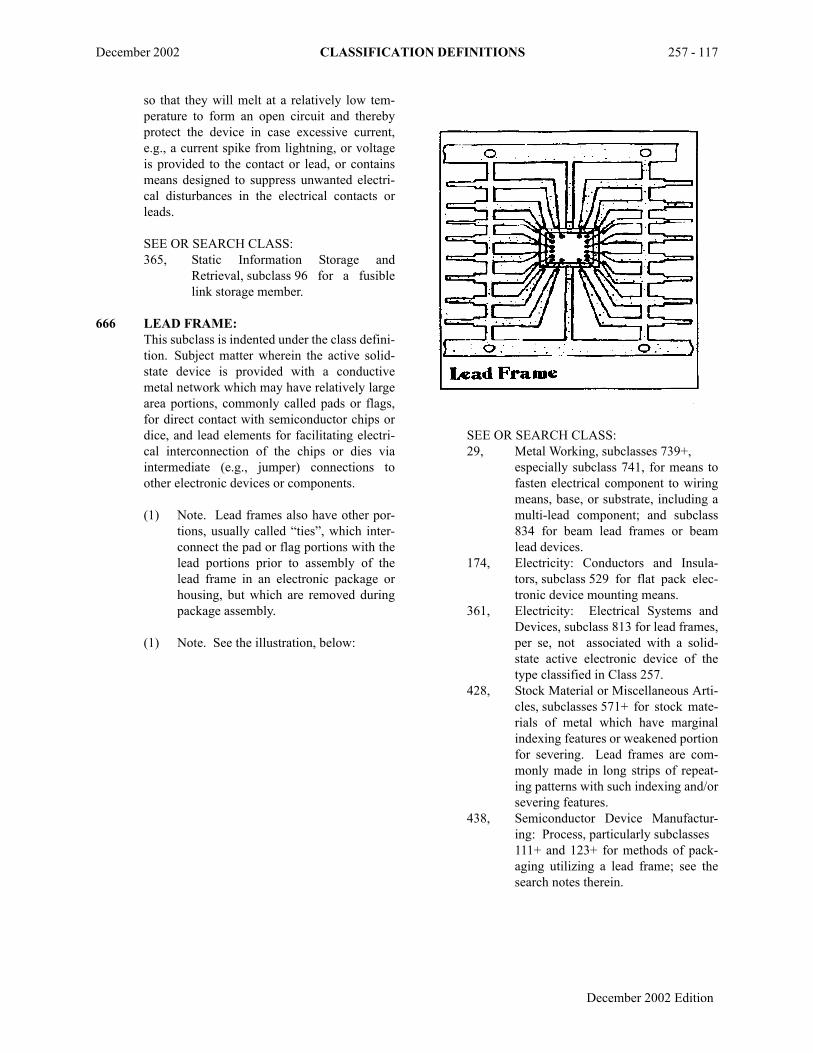
December 2002 CLASSIFICATION DEFINITIONS 257 - 117
so that they will melt at a relatively low tem-perature to form an open circuit and therebyprotect the device in case excessive current,e.g., a current spike from lightning, or voltageis provided to the contact or lead, or containsmeans designed to suppress unwanted electri-cal disturbances in the electrical contacts orleads.
SEE OR SEARCH CLASS:365, Static Information Storage and
Retrieval, subclass 96 for a fusiblelink storage member.
666 LEAD FRAME:This subclass is indented under the class defini-tion. Subject matter wherein the active solid-state device is provided with a conductivemetal network which may have relatively largearea portions, commonly called pads or flags,for direct contact with semiconductor chips ordice, and lead elements for facilitating electri-cal interconnection of the chips or dies viaintermediate (e.g., jumper) connections toother electronic devices or components.
(1) Note. Lead frames also have other por-tions, usually called “ties”, which inter-connect the pad or flag portions with thelead portions prior to assembly of thelead frame in an electronic package orhousing, but which are removed duringpackage assembly.
(1) Note. See the illustration, below:
SEE OR SEARCH CLASS:29, Metal Working, subclasses 739+,
especially subclass 741, for means tofasten electrical component to wiringmeans, base, or substrate, including amulti-lead component; and subclass834 for beam lead frames or beamlead devices.
174, Electricity: Conductors and Insula-tors, subclass 529 for flat pack elec-tronic device mounting means.
361, Electricity: Electrical Systems andDevices, subclass 813 for lead frames,per se, not associated with a solid-state active electronic device of thetype classified in Class 257.
428, Stock Material or Miscellaneous Arti-cles, subclasses 571+ for stock mate-rials of metal which have marginalindexing features or weakened portionfor severing. Lead frames are com-monly made in long strips of repeat-ing patterns with such indexing and/orsevering features.
438, Semiconductor Device Manufactur-ing: Process, particularly subclasses111+ and 123+ for methods of pack-aging utilizing a lead frame; see thesearch notes therein.
December 2002 Edition

257 - 118 CLASSIFICATION DEFINITIONS December 2002
667 With dam or vent for encapsulant:This subclass is indented under subclass 666.Subject matter with a portion or portions toblock encapsulant flow, typically from flowingout of a mold during an encapsulation process,or vent means (e.g., grooves in lead frameleads) to permit egress to the atmosphere for airor other gases which are inside a mold duringencapsulation.
668 On insulating carrier other than a printedcircuit board:This subclass is indented under subclass 666.Subject matter wherein the lead frame ismounted on an insulating carrier other than aprinted circuit board.
(1) Note. Printed circuit boards alone, orwith one or more solid-state electronicdevices mounted thereon are not classi-fied herein, but are found in Class 174,Electricity: Conductors and Insulators,or Class 361, Electricity: Electrical Sys-tems and Devices. See the class defini-tions for Classes 174 and 361 for the lineof demarkation between these twoclasses.
SEE OR SEARCH CLASS:174, Electricity: Conductors and Insula-
tors, subclasses 260 and 520 forprinted circuit boards in combinationwith one or more electronic solid-statedevices.
669 With stress relief:This subclass is indented under subclass 666.Subject matter wherein means are provided toalleviate stresses and strains (e.g., mechanicalor thermal stresses) to which a lead frame issubjected.
670 With separate tie bar element or plural tiebars:This subclass is indented under subclass 666.Subject matter in which a frame element usedto tie or connect a semiconductor chip pad/flagand/or lead fingers frame members is a sepa-rate element and not part of the lead frameitself or wherein plural tie bar elements are pro-vided as part of a lead frame.
671 Of insulating material:This subclass is indented under subclass 670.Subject matter wherein the separate tie bar ele-ment or the plural tie bars are made of electri-cally insulating material.
672 Small lead frame (e.g., “spider” frame) forconnecting a large lead frame to a semicon-ductor chip:This subclass is indented under subclass 666.Subject matter wherein the means used to inter-connect a chip or die to a large lead frame is asmall lead frame with contact elements radiat-ing from a central location for interconnectionwith a chip mounted on a large lead frame chippad at that location to peripheral locations forinterconnection with large lead frame leads.
673 With bumps on ends of lead fingers to con-nect to semiconductor:This subclass is indented under subclass 666.Subject matter wherein bump contacts arelocated at or near the ends of lead fingers toprovide contact with a semiconductor chip.
674 With means for controlling lead tension:This subclass is indented under subclass 666.Subject matter wherein means are provided forcontrolling the tension under which an electri-cal lead is placed including, for example, abend in the lead, an area of reduced lead thick-ness, etc.
675 With heat sink means:This subclass is indented under subclass 666.Subject matter wherein a heat sink means isprovided, either as part of the lead frame or inaddition to the lead frame for cooling the activesolid-state device.
676 With structure for mounting semiconductorchip to lead frame (e.g., configuration of diebonding flag, absence of a die bonding flag,recess for LED):This subclass is indented under subclass 666.Subject matter wherein the lead frame is pro-vided with specified structure means to mounta semiconductor chip thereto, or is specified tonot have a pad for mounting the chip.
(1) Note. This structure may, for example,have a particular configuration such as aflag shape.
1December 2002 Edition

December 2002 CLASSIFICATION DEFINITIONS 257 - 119
677 Of specified material other than copper(e.g., Kovar (T.M.)):This subclass is indented under subclass 666.Subject matter wherein the electrically conduc-tive lead frame is made up of a specific mate-rial other copper, which is a common materialfor lead frames.
678 HOUSING OR PACKAGE:This subclass is indented under the class defini-tion. Subject matter wherein preformed physi-cal means to cover or protect a solid-state elec-tronic device is provided therefor.
SEE OR SEARCH THIS CLASS, SUB-CLASS:81 and 82, for a light emitting device in
combination with or also constitutinga light responsive device and withspecific housing structure.
99 for light emitting device with specifichousing structure.
177 through 182, for a regenerative typeswitching device with housing orexternal electrode.
433 and 434, for light responsive devicewith housing or encapsulation means.
573 for Darlington configuration bipolartransistor structure with housing orcontact structure.
584 for enlarged emitter device bipolartransistor means having housing orcontact.
602 for a voltage variable capacitancedevice with specified housing or con-tact.
660 for means to shield a device containedin a housing.
SEE OR SEARCH CLASS:361, Electricity: Electrical Systems and
Devices, subclass 679.01 for housingsand mounting assemblies for elec-tronic devices and components.
438, Semiconductor Device Manufactur-ing: Process, particularly subclasses106+ for methods of packaging; seethe search notes therein.
679 Smart (e.g., credit) card package:Subject matter under 678 wherein the housingor package is in a form which permits it to beused as a credit card.
(1) Note. A smart card is one which con-tains a microprocessor chip.
SEE OR SEARCH CLASS:235, Registers, subclass 487 and indented
subclasses for coded records includ-ing electronic credit cards, per se.
361, Electricity: Electrical Systems andDevices, subclasses 736+ and 752+for modules for printed circuits orhousing or chassis for printed circuitboards.
680 With window means:Subject matter under 678 wherein the housingor package has a physical opening or area oth-erwise transparent to ultraviolet, visible, orinfrared light.
681 For erasing EPROM:This subclass is indented under subclass 680.Subject matter wherein the window means isprovided for transmitting light to erase an elec-trically programmable read-only memory(EPROM).
682 With desiccant, getter, or gas filling:This subclass is indented under subclass 678.Subject matter including a desiccant (i.e., amaterial for absorbing moisture); a getter (i.e.,a material which absorbs undesirable semicon-ductor, housing or package contaminants); orwherein a gaseous material fills the housing orpackage.
683 With means to prevent explosion of pack-age:This subclass is indented under subclass 678.Subject matter including means to preventexplosion of a housing or package.
684 With semiconductor element forming part(e.g., base, of housing):This subclass is indented under subclass 678.Subject matter wherein part of the housing isformed by a semiconductor element.
(1) Note. The semiconductor element mayhave an inactive portion connected to therest of the housing, and another portionforming an active device, for example.Frequently the semiconductor element
December 2002 Edition

257 - 120 CLASSIFICATION DEFINITIONS December 2002
forms the base of the housing, throughwhich leads are inserted.
685 Multiple housings:This subclass is indented under subclass 678.Subject matter wherein more than one housingis provided for a solid-state active electronicdevice, or wherein plural housings, each con-taining one or more solid-state active devices,are constructed as a unitary structure.
(1) Note. One housing may be locatedwithin another housing.
686 Stacked arrangement:This subclass is indented under subclass 685.Subject matter wherein a plurality of housingsare placed one upon another, vertically.
687 Housing or package filled with solid or liq-uid electrically insulating material:This subclass is indented under subclass 678.Subject matter wherein the housing or packageis filled with a solid or liquid electrically insu-lating material.
(1) Note. Encapsulated devices areexcluded from this subclass and are notconsidered to be housings or packages asdefined in subclass 678 which requiresthem to be preformed.
SEE OR SEARCH CLASS:361, Electricity: Electrical Systems and
Devices, subclasses 729, 730+, and744+ for various modules for printedcircuit boards.
688 With large area flexible electrodes in presscontact with opposite sides of active semi-conductor chip and surrounded by an insu-lating element, e.g., ring:This subclass is indented under subclass 678.Subject matter wherein the package or housinghas two large area electrodes which are in presscontact with opposite sides of a semiconductorchip and wherein the electrode edges are sur-rounded by an electrically insulating medium(e.g., a ring).
(1) Note. Search this class, subclass 181 forsuch housings which specifically containa regenerative active solid-state device(e.g., an SCR or thyristor).
SEE OR SEARCH THIS CLASS, SUB-CLASS:181+, for similar electrodes with regenera-
tive type devices.785 for electrodes combined with an
active semiconductor electronicdevice by pressure alone.
689 Rigid electrode portion:This subclass is indented under subclass 688.Subject matter wherein the large area elec-trodes are rigid in whole or in part.
(1) Note. These type devices typicallyemploy relatively massive electrodes tooperate at large current densities.
690 With contact or lead:This subclass is indented under subclass 678.Subject matter wherein the device is providedwith a contact or lead, in addition to or as partof the package or housing.
691 Having power distribution means (e.g., busstructure):This subclass is indented under subclass 690.Subject matter wherein the contact or leadincludes means for distributing electricalpower to one or more active solid-state deviceswithin the package or housing.
692 With particular lead geometry:This subclass is indented under subclass 690.Subject matter wherein the contact or lead pro-vided as part of or in addition to the package orhousing has a specified geometrical configura-tion.
693 External connection to housing:This subclass is indented under subclass 692.Subject matter wherein the contact or lead hav-ing a specified geometry comprises an electri-cal connection for connecting the package orhousing and its contained active solid-statedevice to other electrical devices or circuits.
694 Axial leads:This subclass is indented under subclass 693.Subject matter wherein the leads or contactswhich form an external connection to the hous-ing or package extend out opposite ends alongan axis of symmetry of a housing or package.
1December 2002 Edition

December 2002 CLASSIFICATION DEFINITIONS 257 - 121
695 Fanned/radial leads:This subclass is indented under subclass 693.Subject matter wherein the leads or contactswhich form an external connection to the hous-ing or package extend radially outward fromthe package.
(1) Note. See illustration, below.
696 Bent (e.g., J-shaped) lead:This subclass is indented under subclass 693.Subject matter wherein the leads or contactswhich form an external connection to the hous-ing or package include one or more leadswhich have a curved end portion (e.g., formounting on the top surface of a printed circuitboard).
(1) Note. See illustration, below.
697 Pin grid type:This subclass is indented under subclass 693.Subject matter wherein the leads or contactswhich form an external connection to the hous-ing or package are in the form of a grid ormatrix of elongated pins.
(1) Note. See illustration, below.
698 With specific electrical feedthrough struc-ture:This subclass is indented under subclass 690.Subject matter wherein a specific structure isprovided for feeding electrical contacts or leadsinto or out of the housing or package.
699 Housing entirely of metal except forfeedthrough structure:Subject matter under 698 wherein the housingor package is made entirely of metal except forthe portion wherein the electrical contacts orleads are fed through.
(1) Note. Typically, an insulator is placed inthe feedthrough portion of a metal hous-ing to prevent electrical short circuitingof the leads to the housing.
700 Multiple contact layers separated from eachother by insulator means and forming partof a package or housing (e.g., plural ceramiclayer package):This subclass is indented under subclass 690.Subject matter wherein the housing or packagecombined with a contact or lead structure is inthe form of a multiple layered insulating com-
December 2002 Edition
257 - 122 CLASSIFICATION DEFINITIONS December 2002
posite with plural electrical connection layerslocated between layers of insulator material.
701 Insulating material:This subclass is indented under subclass 678.Subject matter wherein the housing or packageis made of an electrically insulating material.
702 Of insulating material other than ceramic:Subject matter under 701 wherein the housingis made of electrically insulating material otherthan ceramic (e.g., the housing is made of glassor of a single crystal insulator material).
(1) Note. A ceramic is a polycrystalline,non-metallic, non-organic material, suchas fired polycrystalline aluminum oxide,typically made by firing a compressedand shaped powder at high temperaturesto fuse the powder together.
703 Composite ceramic, or single ceramic withmetal:This subclass is indented under subclass 701.Subject matter wherein the housing is a com-posite made up of at least two ceramic materi-als (e.g., alumina and beryllia) or of a singleceramic material with a metal.
704 Cap or lid:This subclass is indented under subclass 701.Subject matter wherein the housing or packageis provided with a cap or lid.
705 Of high thermal conductivity ceramic (e.g.,BeO):This subclass is indented under subclass 701.Subject matter wherein the housing is made ofceramic which has high thermal conductivity topromote heat dissipation from the housing.
706 With heat sink:This subclass is indented under subclass 701.Subject matter wherein the insulating housinghas a heat sink to dissipate heat.
(1) Note. The heat sink may be located in acavity in a base member made ofceramic material.
SEE OR SEARCH CLASS:174, Electricity: Conductors and Insula-
tors, appropriate subclasses directedto cooling means.
361, Electricity: Electrical Systems andDevices, subclasses 688 through 723 for cooling means for electronicdevices or components with housingsor mounting assemblies.
707 Directly attached to semiconductor device:This subclass is indented under subclass 706.Subject matter wherein the heat sink is attacheddirectly to the semiconductor device.
708 Entirely of metal except for feedthrough:This subclass is indented under subclass 678.Subject matter wherein the housing or packageis made entirely of metal except for the portionwherein the electrical contacts or leads are fedthrough.
(1) Note. Typically, an insulator is placed inthe feedthrough portion of a metal hous-ing to prevent electrical short circuitingof the leads to the housing.
709 With specified insulator to isolate devicefrom housing:This subclass is indented under subclass 708.Subject matter wherein a specific insulatormeans is provided to electrically isolate theactive solid-state device contained in the metalpackage or housing from the metal package orhousing to prevent electrical short circuits dueto the housing or package.
710 With specified means (e.g., lip) to seal baseto cap:This subclass is indented under subclass 708.Subject matter wherein specific means are pro-vided to seal the cap to the base such as, forexample, a bead or lip or boss around theperiphery of the base.
711 With raised portion of base for mountingsemiconductor chip:This subclass is indented under subclass 708.Subject matter wherein a portion of the base israised above the rest of the base and the raisedportion provides a base on which to mount asemiconductor chip with an active solid-statedevice therein or thereon.
1December 2002 Edition
December 2002 CLASSIFICATION DEFINITIONS 257 - 123
712 With provision for cooling the housing or itscontents:This subclass is indented under subclass 678.Subject matter wherein means for cooling thehousing or its contents are provided in additionto natural cooling processes.
SEE OR SEARCH CLASS:174, Electricity: Conductors and Insula-
tors, appropriate subclasses directedto cooling means.
361, Electricity: Electrical Systems andDevices, subclasses 688 through 723,for cooling means for electronicdevices or components with housingsor mounting assemblies.
713 For integrated circuit:This subclass is indented under subclass 712.Subject matter wherein the solid-state elec-tronic device for which cooling means is pro-vided is an integrated circuit, which is asemiconductor substrate which contains a plu-rality of active solid-state electronic devices.
714 Liquid coolant:This subclass is indented under subclass 712.Subject matter wherein the means provided forcooling the housing or its contents is a liquid.
715 Boiling (evaporative) liquid:This subclass is indented under subclass 714.Subject matter wherein the cooling meansinvolves boiling a liquid to provide evaporativecooling.
SEE OR SEARCH CLASS:174, Electricity: Conductors and Insula-
tors, appropriate subclasses directedto liquid cooling means.
361, Electricity: Electrical Systems andDevices, subclasses 699+ for liquidcooling means for electronic devicesor components with housings ormounting assemblies.
716 Cryogenic liquid coolant:This subclass is indented under subclass 714.Subject matter wherein the cooling means usesa liquid to maintain device temperatures at orbelow 100 degrees Kelvin.
SEE OR SEARCH CLASS:174, Electricity: Conductors and Insula-
tors, appropriate subclasses directedto liquid cooling means.
361, Electricity: Electrical Systems andDevices, subclasses 699+ for liquidcooling means for electronic devicesor components with housings ormounting assemblies.
717 Isolation of cooling means (e.g., heat sink)by an electrically insulating element (e.g.,spacer):This subclass is indented under subclass 712.Subject matter wherein an insulating element isused to physically separate a cooling meansfrom an active solid-state electronic device ora housing therefor.
718 Heat dissipating element held in place byclamping or spring means:This subclass is indented under subclass 712.Subject matter wherein an element for dissipat-ing heat is held in place by means to clamp it tothe device or vice versa, or by a spring to posi-tion the device and heat dissipating element inthermal contact with each other.
719 Pressed against semiconductor element:This subclass is indented under subclass 718.Subject matter wherein the heat dissipating ele-ment and the active device are in press contactwith each other.
720 Heat dissipating element has high thermalconductivity insert (e.g., copper slug in alu-minum heat sink):This subclass is indented under subclass 712.Subject matter wherein the heat dissipating ele-ment has a relatively high thermal conductivityvis-a-vis a larger (main) heat sink into which itis inserted (e.g., a copper slug in an aluminumheat sink).
721 With gas coolant:This subclass is indented under subclass 712.Subject matter wherein the cooling means usesa gas to provide the cooling (e.g., by convec-tion).
December 2002 Edition
257 - 124 CLASSIFICATION DEFINITIONS December 2002
722 With fins:This subclass is indented under subclass 721.Subject matter wherein the cooling means hasfins, i.e., long, thin, blade like structures usedto dissipate heat to the gas coolant.
723 For plural devices:This subclass is indented under subclass 678.Subject matter wherein a package or housing isprovided for more than one electronic device,at least one of the electronic devices being anactive solid-state device.
SEE OR SEARCH CLASS:174, Electricity: Conductors and Insula-
tors, subclasses 50+ for housings andprinted circuits.
361, Electricity: Electrical Systems andDevices, subclasses 729 and 730+ forplural housing modules.
724 With discrete components:This subclass is indented under subclass 723.Subject matter wherein at least some of theelectronic components are in the form of anindividual device per semiconductor chip, ascontrasted to a single integrated circuit contain-ing plural semiconductor devices. The discretecomponents may be active solid-state devicesor passive components such as resistors, capac-itors, or inductors.
725 With electrical isolation means:This subclass is indented under subclass 723.Subject matter wherein means are provided toelectrically isolate the plural devices from eachother.
726 Devices held in place by clamping:This subclass is indented under subclass 725.Subject matter wherein the plural deviceswhich are electrically isolated are held in placeby clamp means, i.e., by means which pressdevices into place.
727 Device held in place by clamping:This subclass is indented under subclass 678.Subject matter wherein at least one of the plu-ral devices is held in place by clamp means(i.e., by means which press a device intoplace).
728 For high frequency (e.g., microwave) device:This subclass is indented under subclass 678.Subject matter wherein the active solid-statedevice provided with a housing or package is ahigh frequency solid-state electronic deviceoperating at high frequencies, such as micro-wave frequencies or above.
729 Portion of housing of specific materials:This subclass is indented under subclass 678.Subject matter wherein at least a portion of thehousing or package is made of specific materi-als.
730 Outside periphery of package having speci-fied shape or configuration:This subclass is indented under subclass 678.Subject matter wherein the outside periphery ofa package or housing has a particular shape orconfiguration.
731 With housing mount:This subclass is indented under subclass 678.Subject matter wherein the housing or packagehas means (e.g., a flange or threaded stud) forattaching the housing to a support.
(1) Note. Search this class, subclass 180 forhousings or packages of this type whichspecifically contain a regenerative typeswitching device such as an SCR or thy-ristor.
732 Flanged mount:This subclass is indented under subclass 731.Subject matter wherein the housing mount is aflange with openings therein (e.g., threadedholes) to permit the housing to be attached(e.g., by fasteners) to a support.
733 Stud mount:This subclass is indented under subclass 731.Subject matter wherein the housing mount is athreaded element shaped like a bolt extendingfrom the housing for fastening into a threadedhole in a support.
734 COMBINED WITH ELECTRICAL CON-TACT OR LEAD:This subclass is indented under the class defini-tion. Subject matter wherein the active solid-state device is provided with one or more elec-trical contacts or leads.
1December 2002 Edition

December 2002 CLASSIFICATION DEFINITIONS 257 - 125
SEE OR SEARCH THIS CLASS, SUB-CLASS:41 for point contact rectifiers.44 through 47, for devices with a metal
contact alloyed to elemental semicon-ductor type PN junction in a non-regenerative structure.
54 for Schottky barrier to amorphoussemiconductor material device.
73 for Schottky barrier to polycrystallinesemiconductor material device.
81 and 82, for light emitter combinedwith or also constituting a lightresponsive device and having a spe-cific housing or contact structure.
91 for plural light emitting devices withshaped contacts or opaque masking.
99 for light emitting devices with speci-fied housing or contact structure.
145 for a regenerative type device com-bined with a FET with extended latch-ing current level and a low impedancechannel contact extending below thedevice surface.
155 and 156, for a regenerative typedevice with switching speed enhanc-ing means (e.g., a Schottky contact).
177 through 182, for a regenerative typedevice with housing or external elec-trode.
217 for a majority signal carrier chargetransfer device with a conductivemeans in direct contact with channel(e.g., a non-insulated gate).
260 for JFET having the same channelcontrolled by, for example, Schottkybarrier and pn junction gates.
276 for a JFET in a microwave integratedcircuit with a contact or heat sinkextending through a hole in the semi-conductor.
280 through 284, for JFETs with aSchottky gate electrode.
316 through 322, for a variable thresholdinsulated electrical field effect devicewith additional contacted control elec-trode.
343 for graded channel dopant IGFETdevice with plural sections connectedin parallel and having all contacts onthe same surface.
382 through 385, for an IGFET in an inte-grated circuit with a refractory mate-rial contact to source or drain region.
449 through 457, for Schottky contacts inlight responsive devices.
471 through 486, for Schottky contactdevices.
502 for high power integrated circuitdevices with electrical isolation and abackside collector contact.
503 for an integrated circuit device withelectrically isolated components hav-ing a contact or metallization configu-ration to reduce parasitic coupling.
522 for beam-lead supported semiconduc-tor islands in integrated circuits.
573 for Darlington configuration non-iso-lated bipolar transistors with resis-tance means connected betweentransistor base regions and with hous-ing or contact structure or configura-tion.
576 for complementary bipolar transistorssharing a common active region (e.g.,
IIL, I2L) including lateral bipolartransistor structure and having con-tacts of a refractory material.
584 for bipolar transistor device withenlarged emitter area and with hous-ing or contact means.
602 for a voltage variable capacitancedevice with specified housing or con-tact.
621 for a semiconductor device with elec-trical contact in a hole in the semicon-ductor (e.g., lead extends throughsemiconductor body).
624 for mesa structure device having alow resistance ohmic connectionalong a mesa edge.
661 through 663, for superconductive con-tacts or leads.
664 for transmission line leads.665 for contacts or leads including fusible
link or noise suppression means.666 through 677, for lead frames.688 and 689, for housings with large area
flexible electrodes in press contactwith opposite sides of active semicon-ductor chip and surrounded by aninsulating element.
690 through 700, for housings with speci-fied contact or lead.
December 2002 Edition

257 - 126 CLASSIFICATION DEFINITIONS December 2002
905 for plural DRAM cells sharing a com-mon contact or common trench.
926 for a device with an elongated leadextending axially through anotherelongated lead.
928 for shorted pn or Schottky junctionother than an emitter junction.
SEE OR SEARCH CLASS:174, Electricity: Conductors and Insula-
tors, subclasses 99+ for bus bar struc-ture, per se.
361, Electricity: Electrical Systems andDevices, subclasses 772 through 776 for specific lead configurations con-necting electronic systems anddevices to printed circuit boards.
735 Beam leads (i.e., leads that extend beyondthe ends or sides of a chip component):This subclass is indented under subclass 734.Subject matter wherein electrical contact leadsextend like beams beyond the ends of a chipcomponent.
SEE OR SEARCH CLASS:438, Semiconductor Device Manufactur-
ing: Process, particularly subclass411 for methods of forming electri-cally isolated semiconductor islandsheld in place by beam lead metalliza-tion; subclass 461 for methods offorming beam leads on a semiconduc-tor substrate combined with dicing ofthe substrate into plural separate bod-ies; and subclass 611 for methods offorming beam lead metallization on asemiconductor substrate.
736 Layered:This subclass is indented under subclass 735.Subject matter wherein the leads are made of atleast two separate layers of the same or differ-ent material.
737 Bump leads:This subclass is indented under subclass 734.Subject matter wherein an electrical contact isin the form of a relatively abrupt protuberanceon the surface of a solid-state electronic deviceor chip/die containing such a device.
738 Ball shaped:This subclass is indented under subclass 737.Subject matter wherein the bump contacts havethe spherical shape of a ball.
SEE OR SEARCH THIS CLASS, SUB-CLASS:780 for ball shaped bonds, generally.
739 With textured surface:This subclass is indented under subclass 734.Subject matter wherein the surface of the con-tact or lead is rough or has a characteristic of aclosely interwoven fabric, rather than beingsmooth.
740 With means to prevent contact from pene-trating shallow PN junction (e.g., preventionof aluminum “spiking”):This subclass is indented under subclass 734.Subject matter wherein means are provided forpreventing an electrical contact from penetrat-ing into the relatively thin PN junction region.
(1) Note. This penetration is sometimesreferred to as “spiking”, and if the con-tact material is aluminum, prevention ofthis phenomenon is known as preventionof aluminum spiking.
741 Of specified material other than unalloyedaluminum:This subclass is indented under subclass 734.Subject matter wherein the contact or lead ismade of a specified material other than an alu-minum alloy.
742 With a semiconductor conductivity substitu-tion type dopant (e.g., germanium in thecase of a gallium arsenide semiconductor) ina contact metal):This subclass is indented under subclass 741.Subject matter wherein the contact metal isdoped with atoms of an element, e.g., germa-nium in the case of a semiconductor of galliumarsenide, which changes the conductivity of(i.e., introduces holes or electrons into) thesemiconductor material to which the contact isconnected.
1December 2002 Edition

December 2002 CLASSIFICATION DEFINITIONS 257 - 127
743 For compound semiconductor material:This subclass is indented under subclass 742.Subject matter in which the electrical contactmaterial contacts and contains a dopant for asemiconductor material which is a chemicalcompound, as contrasted to an elemental semi-conductor.
744 For compound semiconductor material:This subclass is indented under subclass 741.Subject matter in which the electrical contactmaterial contacts a semiconductor materialwhich is a chemical compound, as contrastedto an elemental semiconductor.
745 Contact for III-V material:This subclass is indented under subclass 744.Subject matter in which the compound semi-conductor material is a group III-V compound,i.e., one component is from periodic tablegroup III and the other is from periodic tablegroup V.
746 Composite material (e.g., fibers or strandsembedded in solid matrix):This subclass is indented under subclass 741.Subject matter in which the semiconductorcontact material is formed as a composite of,for example, fibers or strands embedded in asolid matrix.
747 With thermal expansion matching of contactor lead material to semiconductor activedevice:This subclass is indented under subclass 741.Subject matter in which the electrical contactor lead material is chosen to have a coefficientof thermal expansion which closely matchesthat of the semiconductor active device mate-rial.
SEE OR SEARCH THIS CLASS, SUB-CLASS:178 for regenerative device with housing
and means to avoid stress (e.g., ther-mal matching of electrode to semicon-ductor).
633 for thermal expansion compensationbetween semiconductor and insulatingcoating.
748 Plural layers of specified contact or leadmaterial:This subclass is indented under subclass 747.Subject matter wherein the thermal expansionmatching lead material is layered.
749 At least portion of which is transparent toultraviolet, visible or infrared light:This subclass is indented under subclass 741.Subject matter wherein at least part of the con-tact or lead is transparent to ultraviolet, visible,or infrared light.
SEE OR SEARCH THIS CLASS, SUB-CLASS:59 for FET devices in amorphous mate-
rial with transparent electrode.72 for FET devices in non-single crystal
semiconductor material with transpar-ent electrode.
449 for light responsive devices withtransparent Schottky barrier.
750 Layered:This subclass is indented under subclass 741.Subject matter wherein the specified contactmaterial is layered.
751 At least one layer forms a diffusion barrier:This subclass is indented under subclass 750.Subject matter wherein at least one layer formsa barrier to the diffusion of the contact materialinto the semiconductor or into another contactlayer.
SEE OR SEARCH THIS CLASS, SUB-CLASS:486 for Schottky barrier layers including a
diffusion barrier material.
752 Planarized to top of insulating layer:This subclass is indented under subclass 750.Subject matter wherein a contact or lead and aninsulating layer to which it is connected form asingle planar surface.
753 With adhesion promoting means (e.g., layerof material) to promote adhesion of contactto an insulating layer:This subclass is indented under subclass 750.Subject matter wherein a means, e.g., a layer ofmaterial, is provided to promote adhesion of an
December 2002 Edition

257 - 128 CLASSIFICATION DEFINITIONS December 2002
electrical contact or lead to an insulating sur-face.
754 At least one layer of silicide or polycrystal-line silicon:This subclass is indented under subclass 750.Subject matter wherein at least one layer ofmaterial is made up of a silicide or polycrystal-line silicon.
SEE OR SEARCH THIS CLASS, SUB-CLASS:381 and 538, for polycrystalline silicon
resistive elements connected to activesemiconductor electronic devices.
554 and 588, for bipolar transistor deviceswith a polycrystalline semiconductorconnection electrode.
755 Polysilicon laminated with silicide:This subclass is indented under subclass 754.Subject matter wherein the layers include apolysilicon laminated with a silicide.
(1) Note. Such laminated contacts of poly-silicon and silicide are sometimes called“polycide” contacts.
756 Multiple polysilicon layers:This subclass is indented under subclass 754.Subject matter wherein a layered electricalcontact or lead includes multiple polysiliconlayers.
757 Silicide of refractory or platinum groupmetal:This subclass is indented under subclass 754.Subject matter wherein a layered electricalcontact or lead includes a silicide of a metalfound in groups IVA, VA, VIA or VIIIA (otherthan iron (Fe), nickel (Ni) or cobalt (Co)) of theperiodic table of the elements.
758 Multiple metal levels on semiconductor, sep-arated by insulating layer (e.g., multiplelevel metallization for integrated circuit):This subclass is indented under subclass 750.Subject matter wherein there are plural layersof metal forming electrical contact material,the layers being separated by intervening layersof insulator material.
SEE OR SEARCH THIS CLASS, SUB-CLASS:211 for gate arrays with multi-level metal-
lization.
SEE OR SEARCH CLASS:156, Adhesive Bonding and Miscella-
neous Chemical Manufacture, sub-classes 60+, for processes of unitingplural bodies via an adhesive material.
438, Semiconductor Device Manufactur-ing: Process, particularly subclasses118+ for methods of packaging asemiconductor device including a stepof bonding utilizing an adhesive mate-rial; see the search notes therein.
759 Including organic insulating materialbetween metal levels:This subclass is indented under subclass 758.Subject matter wherein there is at least onelayer of organic insulating material betweendifferent layers of metal. An organic com-pound is one which fulfills the requirements ofthe Class 260 definition, i.e., has a moleculecharacterized by two carbon atoms bondedtogether, one atom of carbon being bonded toat least one atom of hydrogen or a halogen, orone atom or carbon bonded to at least one atomof nitrogen by a single or double bond, certaincompounds such as HCN, CN-CN, HNCO,HNCS, cyanogen halides, cyanamide, ful-minic acid and metal carbides, being excep-tions to this rule.
760 Separating insulating layer is laminate orcomposite of plural insulating materials(e.g., silicon oxide on silicon nitride, siliconoxynitride):This subclass is indented under subclass 758.Subject matter wherein there is at least one sep-arating insulator layer between different metallayers, which separating insulator layer is itselfmade up of plural sublayers, or which separat-ing insulator layer is a composite such as amixture of silicon oxide and silicon nitride.
761 At least one layer containing vanadium, haf-nium, niobium, zirconium, or tantalum:This subclass is indented under subclass 750.Subject matter wherein a layered electricalcontact or lead has at least one layer which
1December 2002 Edition

December 2002 CLASSIFICATION DEFINITIONS 257 - 129
contains vanadium (V), hafnium (Hf), niobium(Nb), zirconium (Zr), or tantalum (Ta).
762 At least one layer containing silver or cop-per:This subclass is indented under subclass 750.Subject matter wherein a layered electricalcontact or lead has at least one layer whichcontains copper (Cu) or silver (Ag).
763 At least one layer of molybdenum, titanium,or tungsten:This subclass is indented under subclass 750.Subject matter wherein a layered electricalcontact or lead has at least one layer of molyb-denum (Mo), titanium (Ti) or tungsten (W).
764 Alloy containing molybdenum, titanium, ortungsten:This subclass is indented under subclass 763.Subject matter wherein at least one layer con-taining molybdenum, titanium, or tungstencontains an alloy thereof.
765 At least one layer of an alloy containing alu-minum:This subclass is indented under subclass 750.Subject matter wherein a layered electricalcontact or lead has at least one layer of an alloycontaining aluminum (Al).
766 At least one layer containing chromium ornickel:This subclass is indented under subclass 750.Subject matter wherein a layered electricalcontact or lead has at least one layer containingchromium (Cr) or nickel (Ni).
767 Resistive to electromigration or diffusion ofthe contact or lead material:This subclass is indented under subclass 741.Subject matter wherein an electrical contact orlead material is adapted to resist electromigra-tion of the contact or lead material, or diffusionof the contact or lead material into the materialto which the contact is attached.
768 Refractory or platinum group metal or alloyor silicide thereof:This subclass is indented under subclass 741.Subject matter wherein the specified contact orlead material is a refractory metal or a platinumgroup metal, i.e., a metal found in groups IVA,VA, VIA or VIIIA (other than iron (Fe), nickel
(Ni) or cobalt (Co)) of the periodic table of theelements or a silicide (i.e., a binary compoundof silicon), usually with a more electropositiveelement or radical, thereof.
769 Platinum group metal or silicide thereof:This subclass is indented under subclass 768.Subject matter wherein the specified contact orlead material is a platinum group metal (i.e.,platinum (Pt), palladium (Pd), rhodium (Rh),ruthenium (Ru), osmium (Os) or iridium (Ir))or a silicide i.e., a binary compound of silicon,usually with a more electropositive element orradical, thereof.
770 Molybdenum, tungsten, or titanium or theirsilicides:This subclass is indented under subclass 768.Subject matter wherein the specified contact orlead material is molybdenum (Mo), tungsten(W), titanium (Ti), or their silicides, (i.e., abinary compound of one of them with silicon).
771 Alloy containing aluminum:This subclass is indented under subclass 741.Subject matter wherein the specific contact orlead material is an alloy containing aluminum(Al).
772 Solder composition:This subclass is indented under subclass 741.Subject matter wherein the specific contact orlead material is a solder composition (i.e., ametal or metallic alloy that melts at relativelylow temperatures).
(1) Note. Solder is normally used to joinmetals with higher melting points thanthe solder composition.
773 Of specified configuration:This subclass is indented under subclass 734.Subject matter in which an electrical contact orlead has a specific configuration or shape.
774 Via (interconnection hole) shape:This subclass is indented under subclass 773.Subject matter wherein the shape or configura-tion of an electrical contact or lead is deter-mined by the shape of a hole through aninsulating layer through which the contactextends.
December 2002 Edition

257 - 130 CLASSIFICATION DEFINITIONS December 2002
775 Varying width or thickness of conductor:This subclass is indented under subclass 773.Subject matter wherein an electrical contact orlead has a width or thickness which varies overthe length of the contact or lead.
776 Cross-over arrangement, component orstructure:This subclass is indented under subclass 773.Subject matter wherein means are provided forelectrically insulating electrical contact ele-ments or leads which cross each other to do sowithout a short circuit therebetween.
(1) Note. Electrically insulating compo-nents or structures associated with elec-trical contact crossovers may be referredto as bridges, tunnels, overpasses, under-passes, etc.
777 Chip mounted on chip:This subclass is indented under subclass 734.Subject matter wherein a semiconductor sub-strate of an active solid-state device is electri-cally connected to, and positioned on, anothersemiconductor substrate.
SEE OR SEARCH CLASS:361, Electricity: Electrical Systems and
Devices, subclasses 760+ for pluralmodules or means of connection ofcomponents to a printed circuitboard.
778 Flip chip:This subclass is indented under subclass 734.Subject matter wherein a semiconductor sub-strate which contains an active solid-state elec-tronic device has electric contacts on the topside thereof, the top side being that which con-tains an active solid-state electronic device,and which is flipped so that the contact sidebecomes the bottom side for connection with asubstrate which has matching electrical con-tacts.
779 Solder wettable contact, lead, or bond:This subclass is indented under subclass 734.Subject matter wherein an electrical contact orlead has a surface to which solder will readilyadhere.
780 Ball or nail head type contact, lead, or bond:This subclass is indented under subclass 734.Subject matter wherein a contact, lead, or bondis in the form of a wire having an end for con-nection to the semiconductor which is in theshape of a ball or nail head.
SEE OR SEARCH THIS CLASS, SUB-CLASS:738 for ball shaped bump contacts.
781 Layered contact, lead or bond:This subclass is indented under subclass 780.Subject matter wherein a ball or nail head typecontact is made up of a plurality of layers ofthe same or different material.
782 Die bond:This subclass is indented under subclass 734.Subject matter wherein a semiconductor chipcontaining at least one active solid-state deviceand provided with a contact or lead is providedwith a means for attaching the chip to a sup-porting member.
(1) Note. The supporting member or attach-ment may form part of the contacts orleads for the chip, or be separate there-from.
783 With adhesive means:This subclass is indented under subclass 782.Subject matter wherein adhesive means (e.g., alayer) is provided to secure a die (chip) whichcontains an active solid-state electronic deviceto a supporting member.
SEE OR SEARCH CLASS:156, Adhesive Bonding and Miscella-
neous Chemical Manufacture, sub-classes 60+ for processes of unitingplural bodies via an adhesive material.
438, Semiconductor Device Manufactur-ing: Process, particularly subclasses118+ for methods of packaging asemiconductor device including a stepof bonding utilizing an adhesive mate-rial; see the search notes therein.
784 Wire contact, lead, or bond:This subclass is indented under subclass 734.Subject matter wherein the contact, lead orbond is a very flexible, elongated, small diame-
1December 2002 Edition

December 2002 CLASSIFICATION DEFINITIONS 257 - 131
ter filament made of electrically conductivematerial.
785 By pressure alone:This subclass is indented under subclass 734.Subject matter wherein the electrical contact,lead or bond is held in place by pressure alone(e.g., by a spring clip).
SEE OR SEARCH THIS CLASS, SUB-CLASS:181+, and 688+, for other electrodes in press
contact with an active semiconductordevice.
786 Configuration or pattern of bonds:This subclass is indented under subclass 734.Subject matter wherein the electrical contact,lead or bond, has a specific configuration orpattern.
SEE OR SEARCH THIS CLASS, SUB-CLASS:459 for light activated devices with partic-
ular bonding pad arrangement.625 for mesa structure semiconductor
device bonded to heat sink or thickelectrical conductor.
787 ENCAPSULATED:This subclass is indented under the class defini-tion. Subject matter wherein an active solid-state electronic device, often part of a semicon-ductor chip, is surrounded by an electricallyinsulating material which forms a sealedencasement therefor.
SEE OR SEARCH THIS CLASS, SUB-CLASS:100 for encapsulated light emitter device.433+, for light responsive devices with
housing or encapsulation.687 for a housing containing an encapsu-
lant material.
SEE OR SEARCH CLASS:29, Metal Working, particularly sub-
classes 841 and 855 for methods ofassembling an electrical component toa base or lead and encapsulating thesame.
65, Glass Manufacturing, appropriatesubclasses for the manufacturing of
glass encapsulated electronic devicesor components thereof.
174, Electricity: Conductors and Insula-tors, subclass 251 for a printed circuitwith an encapsulated wire.
264, Plastic and Nonmetallic Article Shap-ing or Treating: Processes, subclass272.11 for encapsulation of electricalcomponents.
343, Communications: Radio WaveAntennas, subclass 873 for embed-ded, potted, or coated radio waveantennas.
361, Electricity: Electrical Systems andDevices, subclasses 600 and 679.01for enclosures, including encapsulatedtypes, for electrical and electronicdevices.
438, Semiconductor Device Manufactur-ing: Process, particularly subclasses112 and 127 for methods of encapsu-lating; see the search notes therein.
788 With specified encapsulant:This subclass is indented under subclass 787.Subject matter wherein the chemical composi-tion of the material that encapsulates the activesolid-state electronic device is specified.
789 With specified filler material:This subclass is indented under subclass 788.Subject matter wherein a particular materialhas been added to an encapsulant material togive it desirable mechanical, thermal, electri-cal, or other desirable characteristics, and thematerial is specified.
790 Plural encapsulating layers:This subclass is indented under subclass 788.Subject matter wherein the encapsulant is madeup of more than one layer.
791 Including polysiloxane (e.g., silicone resin):This subclass is indented under subclass 788.Subject matter wherein the encapsulantincludes polysiloxane (i.e., any of variouspolymeric compounds which contain alternatesilicon and oxygen atoms in either a linear orcyclic arrangement), often with one or twoorganic groups attached to each silicon atom.
December 2002 Edition

257 - 132 CLASSIFICATION DEFINITIONS December 2002
792 Including polyimide:This subclass is indented under subclass 788.Subject matter wherein the encapsulantincludes polyimide i.e., a polymeric compoundresulting from replacement of both atoms ofhydrogen in an organic amine by organic uni-valent acid radicals or by an organic divalentacid radical.
(1) Note. Polyimides are copolymers (poly-mers formed from at least two differentstarting organic materials) which have alinkage, as illustrated below, between thestarting materials, wherein R is typicallyhydrogen and Q1 and Q2 are the organic
residues of the starting monomers.
793 Including epoxide:This subclass is indented under subclass 788.Subject matter wherein the encapsulantincludes an epoxy compound (i.e., a compoundcontaining three membered ring consisting orone oxygen and two carbon atoms).
794 Including glass:This subclass is indented under subclass 788.Subject matter wherein the encapsulant con-tains glass (i.e., an amorphous inorganic, usu-ally transparent or translucent substanceconsisting of a mixture of silicates or borates orphosphates formed by fusion of silica or ofoxides of boron or phosphorous with a flux andstabilizer that cools to a rigid condition withoutcrystallization).
795 With specified filler material:This subclass is indented under subclass 787.Subject matter wherein a particular materialhas been added to an encapsulant material togive it desirable mechanical, thermal, electri-cal, or other desirable characteristics, and thematerial is specified.
796 With heat sink embedded in encapsulant:This subclass is indented under subclass 787.Subject matter wherein a heat sink is embeddedin the encapsulant.
SEE OR SEARCH CLASS:174, Electricity: Conductors and Insula-
tors, appropriate subclasses.
361, Electricity: Electrical Systems andDevices, subclasses 704 through 723for thermal conduction means.
797 ALIGNMENT MARKS:This subclass is indented under the class defini-tion. Subject matter wherein the active solid-state device is provided with one or more indi-cia or marks used during fabrication of thedevice to facilitate accurate alignment ofregions in the device.
798 MISCELLANEOUS:This subclass is indented under the class defini-tion. Subject matter wherein the subject matteris not otherwise provided for.
E-SUBCLASSES
NOTE—E-subclasses in USPC Class 257/E47.001-E21.705 were created as duplicates of EPO groups inH01L. With the implementation of CPC, these E-sub-classes should no longer be used. Instead, use CPCgroups H01L 21-51.
The E-subclasses in U.S. Class 257 provide for activesolid-state electronic devices, that is, electronic devicesor components that are made primarily of solid materi-als, usually semiconductors, which operate by themovement of charge carriers - electrons or holes - whichundergo energy level changes within the material andcan modify an input voltage or electro-magnetic signalto achieve rectification, amplification, oscillating, radia-tion emission, or switching action, or capacitors or resis-tors with potential-jump or surface barrier; the E-subclasses include processes or apparatus peculiar to themanufacture or treatment of such active solid-statedevices or of parts of such devices.
E21.001 PROCESSES OR APPARATUS ADAPTEDFOR MANUFACTURE OR TREATMENTOF SEMICONDUCTOR OR SOLID-STATE DEVICES OR OF PARTSTHEREOF: This main group provides for processes orapparatus that are employed in the manufactureor treatment of semiconductor or solid-statedevices or of parts thereof. This subclass issubstantially the same in scope as ECLA clas-sification H01L21/00.
(1) Note. This subclass will take subjectmatter where the manufactured ortreated device/component (or part
1December 2002 Edition

December 2002 CLASSIFICATION DEFINITIONS 257 - 133
thereof) will have at least one of the fol-lowing capabilities:
(a)The conduction or modification of anelectrical current,
(b)The storage of electrical energy forsubsequent discharge within a micro-electronic integrated circuit, or
(c)The conversion of electromagneticwave energy to electrical energy or elec-trical energy to electromagnetic energy.
SEE OR SEARCH THIS CLASS, SUB-CLASS:E31.001,E33.001, E39.001, E45.001, E47.001,
E49.001, and E51.001, for processesor apparatus adapted for manufactureor treatment of semiconductor or solidstate devices or of parts thereof.
E21.002 Manufacture or treatment of semiconductordevice:This subclass is indented under subclassE21.001. This subclass is substantially thesame in scope as ECLA classification H01L21/02.
E21.003 Manufacture of two-terminal component forintegrated circuit:This subclass is indented under subclassE21.002. This subclass is substantially thesame in scope as ECLA classification H01L21/02B.
SEE OR SEARCH THIS CLASS, SUB-CLASS:E21.532,for manufacture or treatment of
devices consisting of a plurality ofsolid-state components formed in oron a common substrate or of partsthereof.
E21.004 Of resistor: This subclass is indented under subclassE21.003. This subclass is substantially thesame in scope as ECLA classification H01L21/02B2.
E21.005 Active material comprising carbon, e.g., dia-mond or diamond-like carbon:This subclass is indented under subclassE21.004. This subclass is substantially the
same in scope as ECLA classification H01L21/02B2D.
E21.006 Active material comprising refractory, tran-sition, or noble metal or metal compound,e.g., alloy, silicide, oxide, nitride: This subclass is indented under subclassE21.004. This subclass is substantially thesame in scope as ECLA classification H01L21/02B2M.
E21.007 Active material comprising organic con-ducting material, e.g., conducting polymer: This subclass is indented under subclassE21.004. This subclass is substantially thesame in scope as ECLA classification H01L21/02B2P.
E21.008 Of capacitor: This subclass is indented under subclassE21.003. This subclass is substantially thesame in scope as ECLA classification H01L21/02B3.
E21.009 Dielectric having perovskite structure: This subclass is indented under subclassE21.008. This subclass is substantially thesame in scope as ECLA classification H01L21/02B3B.
E21.01 Dielectric comprising two or more layers,e.g., buffer layers, seed layers, gradient lay-ers: This subclass is indented under subclassE21.009. This subclass is substantially thesame in scope as ECLA classification H01L21/02B3B2.
E21.011 Formation of electrode: This subclass is indented under subclassE21.008. This subclass is substantially thesame in scope as ECLA classification H01L21/02B3C.
E21.012 With increased surface area, e.g., by rough-ening, texturing: This subclass is indented under subclassE21.011. This subclass is substantially thesame in scope as ECLA classification H01L21/02B3C2.
December 2002 Edition

257 - 134 CLASSIFICATION DEFINITIONS December 2002
E21.013 With rough surface, e.g., using hemispheri-cal grains: This subclass is indented under subclassE21.012. This subclass is substantially thesame in scope as ECLA classification H01L21/02B3C2B.
E21.014 Having cylindrical, crown, or fin-typeshape:This subclass is indented under subclassE21.012. This subclass is substantially thesame in scope as ECLA classification H01L21/02B3C2D.
E21.015 Having horizontal extensions:This subclass is indented under subclassE21.012. This subclass is substantially thesame in scope as ECLA classification H01L21/02B3C2H.
E21.016 Made by depositing layers, e.g., alternat-ingly conductive and insulating layers:This subclass is indented under subclassE21.015. This subclass is substantially thesame in scope as ECLA classification H01L21/02B3C2H2.
E21.017 Made by patterning layers, e.g., etching con-ductive layers:This subclass is indented under subclassE21.015. This subclass is substantially thesame in scope as ECLA classification H01L21/02B3C2H6.
E21.018 Having vertical extensions:This subclass is indented under subclassE21.012. This subclass is substantially thesame in scope as ECLA classification H01L21/02B3C2V.
E21.019 Made by depositing layers, e.g., alternat-ingly conductive and insulating layers:This subclass is indented under subclassE21.018. This subclass is substantially thesame in scope as ECLA classification H01L21/02B3C2V2.
E21.02 Made by patterning layers, e.g., etching con-ductive layers:This subclass is indented under subclassE21.018. This subclass is substantially thesame in scope as ECLA classification H01L21/02B3C2V6.
E21.021 Having multilayers, e.g., comprising barrierlayer and metal layer:This subclass is indented under subclassE21.012. This subclass is substantially thesame in scope as ECLA classification H01L21/02B3C4.
E21.022 Of inductor:This subclass is indented under subclassE21.003. This subclass is substantially thesame in scope as ECLA classification H01L21/02B4.
E21.023 Making mask on semicond uctor body forfurther photolithographic processing: This subclass is indented under subclassE21.002. This subclass is substantially thesame in scope as ECLA classification H01L21/027.
E21.024 Comprising organic layer: This subclass is indented under subclassE21.023. This subclass is substantially thesame in scope as ECLA classification H01L21/027B.
E21.025 For lift-off process: This subclass is indented under subclassE21.024. This subclass is substantially thesame in scope as ECLA classification H01L21/027B2.
E21.026 Characterized by treatment of photoresistlayer: This subclass is indented under subclassE21.024. This subclass is substantially thesame in scope as ECLA classification H01L21/027B6.
E21.027 Photolith ographic process: This subclass is indented under subclassE21.026. This subclass is substantially thesame in scope as ECLA classification H01L21/027B6B.
E21.028 Using laser: This subclass is indented under subclassE21.027. This subclass is substantially thesame in scope as ECLA classification H01L21/027B6B2.
1December 2002 Edition

December 2002 CLASSIFICATION DEFINITIONS 257 - 135
E21.029 Using anti-reflective coating: This subclass is indented under subclassE21.027. This subclass is substantially thesame in scope as ECLA classification H01L21/027B6B4.
E21.03 Electro-lithographic process: This subclass is indented under subclassE21.026. This subclass is substantially thesame in scope as ECLA classification H01L21/027B6C.
E21.031 X-ray lithographic process: This subclass is indented under subclassE21.026. This subclass is substantially thesame in scope as ECLA classification H01L21/027B6D.
E21.032 Ion lithographic process: This subclass is indented under subclassE21.026. This subclass is substantially thesame in scope as ECLA classification H01L21/027B6E.
E21.033 Comprising inorganic layer: This subclass is indented under subclassE21.023. This subclass is substantially thesame in scope as ECLA classification H01L21/033.
E21.034 For lift-off process: This subclass is indented under subclassE21.033. This subclass is substantially thesame in scope as ECLA classification H01L21/033B.
E21.035 Characterized by their composition, e.g.,multilayer masks, materials: This subclass is indented under subclassE21.033. This subclass is substantially thesame in scope as ECLA classification H01L21/033D.
E21.036 Characterized by their size, orientation, dis-position, behavior, shape, in horizontal orvertical plane: This subclass is indented under subclassE21.033. This subclass is substantially thesame in scope as ECLA classification H01L21/033F.
E21.037 Characterized by their behavior during pro-cess, e.g., soluble mask, re-deposited mask: This subclass is indented under subclassE21.036. This subclass is substantially thesame in scope as ECLA classification H01L21/033F2.
E21.038 Characterized by process involved to createmask, e.g., lift-off mask, sidewalls, or tomodify mask, such as pre-treatment, post-treatment: This subclass is indented under subclassE21.036. This subclass is substantially thesame in scope as ECLA classification H01L21/033F4.
E21.039 Process specially adapted to improve theresolution of the mask: This subclass is indented under subclassE21.036. This subclass is substantially thesame in scope as ECLA classification H01L21/033F6.
E21.04 Device having at least one potential-jumpbarrier or surface barrier, e.g., PN junction,depletion layer, carrier concentration layer: This subclass is indented under subclassE21.002. This subclass is substantially thesame in scope as ECLA classification H01L21/04.
E21.041 Device having semiconductor body compris-ing carbon, e.g., diamond, diamond-like car-bon: This subclass is indented under subclassE21.04. This subclass is substantially the samein scope as ECLA classification H01L21/04D.
(1) Note. This group covers passivation ofthe semiconductor body.
E21.042 Making n- or p-doped regions: This subclass is indented under subclassE21.041. This subclass is substantially thesame in scope as ECLA classification H01L21/04D10.
E21.043 Using ion im plantation: This subclass is indented under subclassE21.042. This subclass is substantially thesame in scope as ECLA classification H01L21/04D10B.
December 2002 Edition

257 - 136 CLASSIFICATION DEFINITIONS December 2002
E21.044 Changing their shape, e.g., forming recess: This subclass is indented under subclassE21.041. This subclass is substantially thesame in scope as ECLA classification H01L21/04D16.
E21.045 Making electrode: This subclass is indented under subclassE21.041. This subclass is substantially thesame in scope as ECLA classification H01L21/04D20.
E21.046 Ohmic electrode: This subclass is indented under subclassE21.045. This subclass is substantially thesame in scope as ECLA classification H01L21/04D20A.
E21.047 Schottky electrode: This subclass is indented under subclassE21.045. This subclass is substantially thesame in scope as ECLA classification H01L21/04D20C.
E21.048 Conductor-insulator-semiconductor elec-trode, e.g., MIS contacts: This subclass is indented under subclassE21.045. This subclass is substantially thesame in scope as ECLA classification H01L21/04D20E.
E21.049 Multistep processes for manufacture ofdevice whose active layer, e.g., base, channel,comprises semiconducting carbon, e.g., dia-mond, diamond-like carbon: This subclass is indented under subclassE21.041. This subclass is substantially thesame in scope as ECLA classification H01L21/04D40.
E21.05 Device controllable only by electric currentsupplied or the electric potential applied toelectrode which does not carry current to berectified, amplified, or switched, e.g., three-terminal devices such as source, drain, andgate terminals; emitter, base, collector ter-minals: This subclass is indented under subclassE21.049. This subclass is substantially thesame in scope as ECLA classification H01L21/04D40B.
E21.051 Field-effect transistor: This subclass is indented under subclassE21.05. This subclass is substantially the samein scope as ECLA classification H01L21/04D40B2.
E21.052 Device controllable only by variation ofelectric current supplied or the electricpotential applied to electrodes carrying cur-rent to be rectified, amplified, oscillated, orswitched, e.g., two-terminal device: This subclass is indented under subclassE21.049. This subclass is substantially thesame in scope as ECLA classification H01L21/04D40C.
E21.053 Diode: This subclass is indented under subclassE21.052. This subclass is substantially thesame in scope as ECLA classification H01L21/04D40C2.
E21.054 Device having semiconductor body compris-ing silicon carbide (SiC): This subclass is indented under subclassE21.04. This subclass is substantially the samein scope as ECLA classification H01L21/04H.
E21.055 Passivating silicon carbide surface: This subclass is indented under subclassE21.054. This subclass is substantially thesame in scope as ECLA classification H01L21/04H2.
E21.056 Making n- or p- doped regions or layers,e.g., using diffusion: This subclass is indented under subclassE21.054. This subclass is substantially thesame in scope as ECLA classification H01L21/04H4.
E21.057 Using ion implantation: This subclass is indented under subclassE21.056. This subclass is substantially thesame in scope as ECLA classification H01L21/04H4A.
SEE OR SEARCH THIS CLASS, SUB-CLASS:E21.054,for processes where ion implantation
of boron and subsequent annealingdoes not produce a p-doped region.
1December 2002 Edition

December 2002 CLASSIFICATION DEFINITIONS 257 - 137
E21.058 Using masks: This subclass is indented under subclassE21.057. This subclass is substantially thesame in scope as ECLA classification H01L21/04H4A10.
E21.059 Angled implantation: This subclass is indented under subclassE21.057. This subclass is substantially thesame in scope as ECLA classification H01L21/04H4A12.
E21.06 Changing shape of semiconductor body, e.g.,forming recesses: This subclass is indented under subclassE21.054. This subclass is substantially thesame in scope as ECLA classification H01L21/04H6.
E21.061 Making electrode: This subclass is indented under subclassE21.054. This subclass is substantially thesame in scope as ECLA classification H01L21/04H10.
E21.062 Ohmic electrode: This subclass is indented under subclassE21.061. This subclass is substantially thesame in scope as ECLA classification H01L21/04H10A.
E21.063 Conductor-insulator-semiconductor elec-trode, e.g., MIS contact: This subclass is indented under subclassE21.061. This subclass is substantially thesame in scope as ECLA classification H01L21/04H10B.
E21.064 Schottky electrode: This subclass is indented under subclassE21.061. This subclass is substantially thesame in scope as ECLA classification H01L21/04H10C.
E21.065 Multistep processes for manufacture ofdevice whose active layer, e.g., base, channel,comprises silicon carbide: This subclass is indented under subclassE21.054. This subclass is substantially thesame in scope as ECLA classification H01L21/04H20.
E21.066 Device controllable only by electric currentsupplied or the electric potential applied toelectrode which does not carry current to berectified, amplified, or switched, e.g., three-terminal device: This subclass is indented under subclassE21.065. This subclass is substantially thesame in scope as ECLA classification H01L21/04H20B.
E21.067 Device controllable only by variation ofelectric current supplied or electric potentialapplied to one or more of the electrodes car-rying current to be rectified, amplified,oscillated, or switched, e.g., two-terminaldevice: This subclass is indented under subclassE21.065. This subclass is substantially thesame in scope as ECLA classification H01L21/04H20C.
E21.068 Device having semiconductor body compris-ing selenium (Se) or tellurium (Te): This subclass is indented under subclassE21.04. This subclass is substantially the samein scope as ECLA classification H01L21/06.
E21.069 Preparation of substrate or foundation platefor Se or Te semiconductor: This subclass is indented under subclassE21.068. This subclass is substantially thesame in scope as ECLA classification H01L21/08.
E21.07 Preliminary treatment of Se or Te, its appli-cation to substrate, or the subsequent treat-ment of combination: This subclass is indented under subclassE21.068. This subclass is substantially thesame in scope as ECLA classification H01L21/10.
E21.071 Application of Se or Te to substrate or foun-dation plate: This subclass is indented under subclassE21.07. This subclass is substantially the samein scope as ECLA classification H01L21/10B.
E21.072 Conversion of Se or Te to conductive state: This subclass is indented under subclassE21.07. This subclass is substantially the samein scope as ECLA classification H01L21/103.
December 2002 Edition

257 - 138 CLASSIFICATION DEFINITIONS December 2002
E21.073 Treatment of surface of Se or Te layer afterhaving been made conductive: This subclass is indented under subclassE21.07. This subclass is substantially the samein scope as ECLA classification H01L21/105.
E21.074 Provision of discrete insulating layer, i.e.,specified barrier layer material: This subclass is indented under subclassE21.07. This subclass is substantially the samein scope as ECLA classification H01L21/108.
E21.075 Application of electrode to exposed surfaceof Se or Te after Se or Te has been applied tofoundation plate: This subclass is indented under subclassE21.068. This subclass is substantially thesame in scope as ECLA classification H01L21/12.
E21.076 Treatment of complete device, e.g., by elec-troforming to form barrier: This subclass is indented under subclassE21.068. This subclass is substantially thesame in scope as ECLA classification H01L21/14.
E21.077 Heat treating: This subclass is indented under subclassE21.076. This subclass is substantially thesame in scope as ECLA classification H01L21/145.
E21.078 Device having semiconductor body compris-ing cuprous oxide (Cu2O) or cuprous iodide
(CuI): This subclass is indented under subclassE21.04. This subclass is substantially the samein scope as ECLA classification H01L21/16.
E21.079 Preparation of substrate, preliminary treat-ment oxidation of substrate, reduction treat-ment: This subclass is indented under subclassE21.078. This subclass is substantially thesame in scope as ECLA classification H01L21/16B.
E21.08 Preliminary treatment of foundation plate: This subclass is indented under subclassE21.079. This subclass is substantially thesame in scope as ECLA classification H01L21/16B2.
E21.081 Reduction of copper oxide, treatment ofoxide layer: This subclass is indented under subclassE21.079. This subclass is substantially thesame in scope as ECLA classification H01L21/16B4.
E21.082 Oxidation and subsequent heat treatment ofsubstrate: This subclass is indented under subclassE21.079. This subclass is substantially thesame in scope as ECLA classification H01L21/16B3.
E21.083 Application of specified conductive layer: This subclass is indented under subclassE21.079. This subclass is substantially thesame in scope as ECLA classification H01L21/16B5.
E21.084 Treatment of complete device, e.g., electro-forming, heat treating: This subclass is indented under subclassE21.078. This subclass is substantially thesame in scope as ECLA classification H01L21/16C.
E21.085 Device having semiconductor body compris-ing Group IV elements or Group III-V com-pounds with or without impurities, e.g.,doping materials: This subclass is indented under subclassE21.04. This subclass is substantially the samein scope as ECLA classification H01L21/18.
(1) Note. This group covers also processeswhich, by using the appropriate technol-ogy, are clearly suitable for manufactureor treatment of devices whose bodiescomprise Group IV elements or III-Vcompounds, even if the material used isnot explicitly specified.
E21.086 Intermixing or interdiffusion or disorderingof Group III-V heterostructures, e.g., IILD: This subclass is indented under subclassE21.085. This subclass is substantially thesame in scope as ECLA classification H01L21/18A.
1December 2002 Edition

December 2002 CLASSIFICATION DEFINITIONS 257 - 139
E21.087 Joining of semiconductor body for junctionformation: This subclass is indented under subclassE21.085. This subclass is substantially thesame in scope as ECLA classification H01L21/18B.
E21.088 By direct bonding: This subclass is indented under subclassE21.087. This subclass is substantially thesame in scope as ECLA classification H01L21/18B2.
E21.089 Multistep processes for manufacture ofdevice using quantum interference effect,e.g., electrostatic Aharonov-Bohm effect: This subclass is indented under subclassE21.085. This subclass is substantially thesame in scope as ECLA classification H01L21/18Q.
E21.09 Deposition of semiconductor material onsubstrate, e.g., epitaxial growth, solid phaseepitaxy: This subclass is indented under subclassE21.085. This subclass is substantially thesame in scope as ECLA classification H01L21/20.
E21.091 Using physical deposition, e.g., vacuumdeposition, sputtering: This subclass is indented under subclassE21.09. This subclass is substantially the samein scope as ECLA classification H01L21/203.
E21.092 Epitaxial deposition of Group IV element,e.g., Si, Ge: This subclass is indented under subclassE21.091. This subclass is substantially thesame in scope as ECLA classification H01L21/203B.
E21.093 Deposition on semiconductor substratebeing different from deposited semiconduc-tor material; i.e., formation of heterojunc-tions: This subclass is indented under subclassE21.092. This subclass is substantially thesame in scope as ECLA classification H01L21/203B2.
E21.094 Deposition on insulating or meta llic sub-strate: This subclass is indented under subclassE21.092. This subclass is substantially thesame in scope as ECLA classification H01L21/203B3.
E21.095 Epitaxial deposition of diamond: This subclass is indented under subclassE21.092. This subclass is substantially thesame in scope as ECLA classification H01L21/203B4.
E21.096 Deposition of diamond: This subclass is indented under subclassE21.091. This subclass is substantially thesame in scope as ECLA classification H01L21/203A.
E21.097 Epitaxial deposition of Group III-V com-pound: This subclass is indented under subclassE21.091. This subclass is substantially thesame in scope as ECLA classification H01L21/203C.
E21.098 Deposition on semiconductor substrate notbeing an Group III-V compound: This subclass is indented under subclassE21.097. This subclass is substantially thesame in scope as ECLA classification H01L21/203C2.
E21.099 Deposition on insulating or metallic sub-strate: This subclass is indented under subclassE21.097. This subclass is substantially thesame in scope as ECLA classification H01L21/203C3.
E21.1 Doping during epitaxial deposition: This subclass is indented under subclassE21.097. This subclass is substantially thesame in scope as ECLA classification H01L21/203C6.
E21.101 Using reduction or decomposition of gaseouscompound yielding solid condensate, i.e.,chemical deposition: This subclass is indented under subclassE21.09. This subclass is substantially the samein scope as ECLA classification H01L21/205.
December 2002 Edition

257 - 140 CLASSIFICATION DEFINITIONS December 2002
E21.102 Epitaxial deposition of Group IV elements,e.g., Si, Ge, C: This subclass is indented under subclassE21.101. This subclass is substantially thesame in scope as ECLA classification H01L21/205B.
E21.103 Deposition on a semiconductor substratewhich is different from the semiconductormaterial being deposited, i.e., formation ofheterojunctions: This subclass is indented under subclassE21.102. This subclass is substantially thesame in scope as ECLA classification H01L21/205B2.
E21.104 Deposition on an insulating or a metallicsubstrate: This subclass is indented under subclassE21.102. This subclass is substantially thesame in scope as ECLA classification H01L21/205B3.
E21.105 Epitaxial deposition of diamond: This subclass is indented under subclassE21.102. This subclass is substantially thesame in scope as ECLA classification H01L21/205B4.
E21.106 Doping during the epitaxial deposition: This subclass is indented under subclassE21.102. This subclass is substantially thesame in scope as ECLA classification H01L21/205B6.
E21.107 Deposition of diamond: This subclass is indented under subclassE21.101. This subclass is substantially thesame in scope as ECLA classification H01L21/205A.
E21.108 Epitaxial deposition of Group III-V com-pound: This subclass is indented under subclassE21.101. This subclass is substantially thesame in scope as ECLA classification H01L21/205C.
E21.109 Using molecular beam technique: This subclass is indented under subclassE21.108. This subclass is substantially thesame in scope as ECLA classification H01L21/205C4.
E21.11 Doping the epitaxial deposit: This subclass is indented under subclassE21.108. This subclass is substantially thesame in scope as ECLA classification H01L21/205C6.
E21.111 Doping with transition metals to form semi-insulating layers: This subclass is indented under subclassE21.11. This subclass is substantially the samein scope as ECLA classification H01L21/205C6B.
E21.112 Deposition on a semiconductor substrate notbeing Group III-V compound: This subclass is indented under subclassE21.108. This subclass is substantially thesame in scope as ECLA classification H01L21/205C2.
E21.113 Deposition on an insulating or a metallicsubstrate:This subclass is indented under subclassE21.108. This subclass is substantially thesame in scope as ECLA classification H01L21/205C3.
E21.114 Using liquid deposition: This subclass is indented under subclassE21.09. This subclass is substantially the samein scope as ECLA classification H01L21/208.
E21.115 Epitaxial deposition of Group IV elements,e.g., Si, Ge, C: This subclass is indented under subclassE21.114. This subclass is substantially thesame in scope as ECLA classification H01L21/208B.
E21.116 Deposition on a semiconductor substratewhich is different from the semiconductormaterial being deposited, i.e., formation ofheterojunction: This subclass is indented under subclassE21.115. This subclass is substantially thesame in scope as ECLA classification H01L21/208B2.
E21.117 Epitaxial deposition of Group III-V com-pound: This subclass is indented under subclassE21.114. This subclass is substantially the
1December 2002 Edition
December 2002 CLASSIFICATION DEFINITIONS 257 - 141
same in scope as ECLA classification H01L21/208C.
E21.118 Deposition on a semiconductor substrate notbeing an Group III-V compound: This subclass is indented under subclassE21.117. This subclass is substantially thesame in scope as ECLA classification H01L21/208C2.
E21.119 Characterized by the substrate: This subclass is indented under subclassE21.09. This subclass is substantially the samein scope as ECLA classification H01L21/20B.
E21.12 Characterized by the post-treatment used tocontrol the interface betw een substrate andepitaxial layer, e.g., ion implantation fol-lowed by annealing: This subclass is indented under subclassE21.119. This subclass is substantially thesame in scope as ECLA classification H01L21/20B20.
E21.121 Substrate is crystalline insulating material,e.g., sapphire: This subclass is indented under subclassE21.119. This subclass is substantially thesame in scope as ECLA classification H01L21/20B4.
E21.122 Bonding of semiconductor wafer to insulat-ing substrate or to semic onducting sub-strate using an intermediate insulatinglayer: This subclass is indented under subclassE21.119. This subclass is substantially thesame in scope as ECLA classification H01L21/20B2.
SEE OR SEARCH THIS CLASS, SUB-CLASS:E21.088,for bonding of semiconductor wafer
to semiconductor wafer for junctionformation.
E21.123 Substrate is crystalline semiconductor mate-rial, e.g., lattice adaptation, heteroepitaxy: This subclass is indented under subclassE21.119. This subclass is substantially thesame in scope as ECLA classification H01L21/20B6.
E21.124 Heteroepitaxy: This subclass is indented under subclassE21.123. This subclass is substantially thesame in scope as ECLA classification H01L21/20B6B.
E21.125 Defect and dislocati on suppression due tolattice mismatch, e.g., lattice adaptation: This subclass is indented under subclassE21.124. This subclass is substantially thesame in scope as ECLA classification H01L21/20B6B2.
E21.126 Group III-V compound on dissimilar GroupIII-V compound: This subclass is indented under subclassE21.124. This subclass is substantially thesame in scope as ECLA classification H01L21/20B6B4.
E21.127 Group III-V compound on Si or Ge: This subclass is indented under subclassE21.124. This subclass is substantially thesame in scope as ECLA classification H01L21/20B6B6.
E21.128 Carbon on a noncarbon semiconductor sub-strate: This subclass is indented under subclassE21.124. This subclass is substantially thesame in scope as ECLA classification H01L21/20B6B10.
E21.129 Group IVA, e.g., Si, C, Ge on Group IVB,e.g., Ti, Zr: This subclass is indented under subclassE21.124. This subclass is substantially thesame in scope as ECLA classification H01L21/20B6B8.
E21.13 The substrate is crystalline conductingmaterial, e.g., metallic silicide: This subclass is indented under subclassE21.119. This subclass is substantially thesame in scope as ECLA classification H01L21/20B8.
E21.131 Selective epilaxial growth, e.g., simultaneousdeposition of mono- and non-mono semicon-ductor material: This subclass is indented under subclassE21.09. This subclass is substantially the samein scope as ECLA classification H01L21/20C.
December 2002 Edition

257 - 142 CLASSIFICATION DEFINITIONS December 2002
E21.132 Preparation of substrate for selective epi-taxy : This subclass is indented under subclassE21.131. This subclass is substantially thesame in scope as ECLA classification H01L21/20C2.
E21.133 Epitaxial re-growth of non-monocrystallinesemiconductor material, e.g., lateral epitaxyby seeded solidific ation, solid-state crystalli-zation, solid-state graphoepitaxy, explosivecrystallization, grain growth in polycrystal-line material: This subclass is indented under subclassE21.09. This subclass is substantially the samein scope as ECLA classification H01L21/20D.
E21.134 Using a coherent energy beam, e.g., laser orelectron beam: This subclass is indented under subclassE21.133. This subclass is substantially thesame in scope as ECLA classification H01L21/20D2.
E21.135 Diffusion of impurity material, e.g., dopingmaterial, electrode material, into or out of asemiconductor body, or between semicon-ductor regions; interactions between two ormore impurities; redistribution of impuri-ties: This subclass is indented under subclassE21.085. This subclass is substantially thesame in scope as ECLA classification H01L21/22.
E21.136 From the substrate during epitaxy, e.g., aut-odoping; preventing or using autodoping: This subclass is indented under subclassE21.135. This subclass is substantially thesame in scope as ECLA classification H01L21/22C.
E21.137 To control carrier lifetime, i.e., deep leveldopant: This subclass is indented under subclassE21.135. This subclass is substantially thesame in scope as ECLA classification H01L21/22D.
E21.138 In Group III-V compound: This subclass is indented under subclassE21.137. This subclass is substantially the
same in scope as ECLA classification H01L21/22D2.
E21.139 Lithium-drift: This subclass is indented under subclassE21.135. This subclass is substantially thesame in scope as ECLA classification H01L21/22L.
E21.14 Diffusion source: This subclass is indented under subclassE21.135. This subclass is substantially thesame in scope as ECLA classification H01L21/22N.
E21.141 Using diffusion into or out of a solid from orinto a gaseous phase: This subclass is indented under subclassE21.135. This subclass is substantially thesame in scope as ECLA classification H01L21/223.
SEE OR SEARCH THIS CLASS, SUB-CLASS:E21.144,for diffusion into or out of a solid
from or into a solid phase, e.g., adoped oxide layer.
E21.142 Diffusion into or out of Group III-V com-pound: This subclass is indented under subclassE21.141. This subclass is substantially thesame in scope as ECLA classification H01L21/223B.
E21.143 From or into plasma phase: This subclass is indented under subclassE21.141. This subclass is substantially thesame in scope as ECLA classification H01L21/223E.
E21.144 Using diffusion into or out of a solid from orinto a solid phase, e.g., a doped oxide layer:This subclass is indented under subclassE21.135. This subclass is substantially thesame in scope as ECLA classification H01L21/225.
E21.145 Diffusion into or out of Group IV semicon-ductor: This subclass is indented under subclassE21.144. This subclass is substantially thesame in scope as ECLA classification H01L21/225A.
1December 2002 Edition

December 2002 CLASSIFICATION DEFINITIONS 257 - 143
E21.146 Using predeposition of impurities into thesemiconductor surface, e.g., from gaseousphase: This subclass is indented under subclassE21.145. This subclass is substantially thesame in scope as ECLA classification H01L21/225A2.
E21.147 By ion implantation: This subclass is indented under subclassE21.146. This subclass is substantially thesame in scope as ECLA classification H01L21/225A2D.
E21.148 From or through or into an applied layer,e.g., photoresist, nitride: This subclass is indented under subclassE21.145. This subclass is substantially thesame in scope as ECLA classification H01L21/225A4.
E21.149 Applied layer is oxide, e.g., P2O5, PSG, H3BO3, doped oxide: This subclass is indented under subclassE21.148. This subclass is substantially thesame in scope as ECLA classification H01L21/225A4D.
E21.15 Through the applied layer: This subclass is indented under subclassE21.149. This subclass is substantially thesame in scope as ECLA classification H01L21/225A4D2.
E21.151 Applied layer being silicon or silicide orSIPOS, e.g., polysilicon, porous silicon: This subclass is indented under subclassE21.148. This subclass is substantially thesame in scope as ECLA classification H01L21/225A4F.
E21.152 Diffusion into or out of Group III-V com-pound: This subclass is indented under subclassE21.144. This subclass is substantially thesame in scope as ECLA classification H01L21/225B.
E21.153 Using diffusion into or out of a solid from orinto a liquid phase, e.g., alloy diffusion pro-cess: This subclass is indented under subclassE21.135. This subclass is substantially the
same in scope as ECLA classification H01L21/228.
E21.154 Alloying of impurity material, e.g., dopingmaterial, electrode material, with a semicon-ductor body: This subclass is indented under subclassE21.085. This subclass is substantially thesame in scope as ECLA classification H01L21/24.
E21.155 Alloying of doping material with Group III-V compound: This subclass is indented under subclassE21.154. This subclass is substantially thesame in scope as ECLA classification H01L21/24B.
E21.156 Alloying of electrode material: This subclass is indented under subclassE21.154. This subclass is substantially thesame in scope as ECLA classification H01L21/24C.
E21.157 With Group III-V compound: This subclass is indented under subclassE21.156. This subclass is substantially thesame in scope as ECLA classification H01L21/24C2.
E21.158 Manufacture of electrode on semiconductorbody using process other than by epitaxialgrowth, diffusion of impurities, alloying ofimpurity materials, or radiation bombard-ment: This subclass is indented under subclassE21.085. This subclass is substantially thesame in scope as ECLA classification H01L21/28.
SEE OR SEARCH THIS CLASS, SUB-CLASS:E21.090 through E21.134, for epitaxial
growth.E21.135 through E21.153, for diffusion of
impurities. E21.154 through E21 -157, for alloying of
impurity materials.E21.328 through E21.349, for radiation bom-
bardment. E21.249 through E21.257 and E21.305-
E21.314, for etching and patterningthe electrodes.
December 2002 Edition

257 - 144 CLASSIFICATION DEFINITIONS December 2002
E21.159 Deposition of conductive or insulating mate-rial for electrode conducting electric cur-rent: This subclass is indented under subclassE21.158. This subclass is substantially thesame in scope as ECLA classification H01L21/283.
E21.16 From a gas or vapor, e.g., condensation : This subclass is indented under subclassE21.159. This subclass is substantially thesame in scope as ECLA classification H01L21/285.
E21.161 Of conductive layer: This subclass is indented under subclassE21.16. This subclass is substantially the samein scope as ECLA classification H01L21/285B.
E21.162 On semiconductor body comprising GroupIV element: This subclass is indented under subclassE21.161. This subclass is substantially thesame in scope as ECLA classification H01L21/285B4.
E21.163 Deposition of Schottky electrode: This subclass is indented under subclassE21.162. This subclass is substantially thesame in scope as ECLA classification H01L21/285B4C.
E21.164 O layer comprising silicide: This subclass is indented under subclassE21.162. This subclass is substantially thesame in scope as ECLA classification H01L21/285B4D.
E21.165 Conductive layer comprising silicide: This subclass is indented under subclassE21.162. This subclass is substantially thesame in scope as ECLA classification H01L21/285B4A.
E21.166 Conductive layer comprising semiconduct-ing material: This subclass is indented under subclassE21.162. This subclass is substantially thesame in scope as ECLA classification H01L21/285B4B.
E21.167 Making of side-wall contact: This subclass is indented under subclassE21.166. This subclass is substantially thesame in scope as ECLA classification H01L21/285B4B2.
E21.168 Conductive layer comprising transitionmetal, e.g., Ti, W, Mo: This subclass is indented under subclassE21.162. This subclass is substantially thesame in scope as ECLA classification H01L21/285B4L.
E21.169 By physical means, e.g., sputtering, evapora-tion: This subclass is indented under subclassE21.162. This subclass is substantially thesame in scope as ECLA classification H01L21/285B4F.
E21.17 By chemical means, e.g., CVD, LPCVD,PECVD, laser CVD: This subclass is indented under subclassE21.162. This subclass is substantially thesame in scope as ECLA classification H01L21/285B4H.
E21.171 Selective deposition: This subclass is indented under subclassE21.17. This subclass is substantially the samein scope as ECLA classification H01L21/285B4H2.
E21.172 On semiconductor body comprising GroupIII-V compound: This subclass is indented under subclassE21.161. This subclass is substantially thesame in scope as ECLA classification H01L21/285B6.
E21.173 Deposition of Schottky electrode: This subclass is indented under subclassE21.172. This subclass is substantially thesame in scope as ECLA classification H01L21/285B6B.
E21.174 From a liquid, e.g., electrolytic deposition: This subclass is indented under subclassE21.159. This subclass is substantially thesame in scope as ECLA classification H01L21/288.
1December 2002 Edition

December 2002 CLASSIFICATION DEFINITIONS 257 - 145
E21.175 Using an external electrical current, i.e.,electro-deposition: This subclass is indented under subclassE21.174. This subclass is substantially thesame in scope as ECLA classification H01L21/288E.
E21.176 Manufacture or post-treatment of electrodehaving a capacitive structure, i.e., gatestructure for field-effect device: This subclass is indented under subclassE21.158. This subclass is substantially thesame in scope as ECLA classification H01L21/28B.
E21.177 MOS-gate structure: This subclass is indented under subclassE21.176. This subclass is substantially thesame in scope as ECLA classification H01L21/28B2.
E21.178 Joint-gate structure: This subclass is indented under subclassE21.177. This subclass is substantially thesame in scope as ECLA classification H01L21/28B2C.
E21.179 Floating or plural gate structure: This subclass is indented under subclassE21.177. This subclass is substantially thesame in scope as ECLA classification H01L21/28B2D.
E21.18 Gate structure with charge-trapping insula-tor: This subclass is indented under subclassE21.177. This subclass is substantially thesame in scope as ECLA classification H01L21/28B2E.
E21.181 On semiconductor body not comprisingGroup IV element, e.g., Group III-V com-pound: This subclass is indented under subclassE21.177. This subclass is substantially thesame in scope as ECLA classification H01L21/28B2F.
E21.182 On semiconductor body comprising GroupIV element excluding non-elemental Si, e.g.,
Ge, C, diamond, silicon compound or com-pound, such as SiC or SiGe: This subclass is indented under subclassE21.177. This subclass is substantially thesame in scope as ECLA classification H01L21/28B2G.
E21.183 For charge-coupled device: This subclass is indented under subclassE21.177. This subclass is substantially thesame in scope as ECLA classification H01L21/28B2K.
E21.184 PN-homojunction gate structure: This subclass is indented under subclassE21.176. This subclass is substantially thesame in scope as ECLA classification H01L21/28B3.
E21.185 For charge-coupled device: This subclass is indented under subclassE21.184. This subclass is substantially thesame in scope as ECLA classification H01L21/28B3K.
E21.186 Schottky gate structure: This subclass is indented under subclassE21.176. This subclass is substantially thesame in scope as ECLA classification H01L21/28B4.
E21.187 For charge-coupled device: This subclass is indented under subclassE21.186. This subclass is substantially thesame in scope as ECLA classification H01L21/28B4K.
E21.188 Heterojunction gate structure: This subclass is indented under subclassE21.176. This subclass is substantially thesame in scope as ECLA classification H01L21/28B5.
E21.189 For charge-coupled device: This subclass is indented under subclassE21.188. This subclass is substantially thesame in scope as ECLA classification H01L21/28B5K.
E21.19 Making electrode structure comprising con-ductor-insulator-semiconductor, e.g., MISgate: This subclass is indented under subclassE21.158. This subclass is substantially the
December 2002 Edition
257 - 146 CLASSIFICATION DEFINITIONS December 2002
same in scope as ECLA classification H01L21/28E.
E21.191 Insulator formed on silicon semiconductorbody: This subclass is indented under subclassE21.19. This subclass is substantially the samein scope as ECLA classification H01L21/28E2.
E21.192 Characterized by insulator: This subclass is indented under subclassE21.191. This subclass is substantially thesame in scope as ECLA classification H01L21/28E2C.
E21.193 On single crystalline silicon: This subclass is indented under subclassE21.192. This subclass is substantially thesame in scope as ECLA classification H01L21/28E2C2.
E21.194 Characterized by treatment after formationof definitive gate conductor: This subclass is indented under subclassE21.193. This subclass is substantially thesame in scope as ECLA classification H01L21/28E2C2B.
E21.195 Characterized by conductor: This subclass is indented under subclassE21.191. This subclass is substantially thesame in scope as ECLA classification H01L21/28E2B.
(1) Note. This subclass includes the finalconductor comprising a superconductor.
E21.196 Final conductor next to insulator havinglateral composition or doping variation, orbeing formed laterally by more than onedeposition step: This subclass is indented under subclassE21.195. This subclass is substantially thesame in scope as ECLA classification H01L21/28E2B8.
E21.197 Final conductor layer next to insulator beingsilicon e.g., polysilicon, with or withoutimpurities: This subclass is indented under subclassE21.195. This subclass is substantially thesame in scope as ECLA classification H01L21/28E2B2.
(1) Note. A very thin layer, e.g., silicon,adhesion or seed layer is not consideredas the one next to the insulator.
E21.198 Conductor comprising at least another non-silicon conductive layer: This subclass is indented under subclassE21.197. This subclass is substantially thesame in scope as ECLA classification H01L21/28E2B2P.
E21.199 Conductor comprising silicide layer formedby silicidation reaction of silicon with metallayer: This subclass is indented under subclassE21.198. This subclass is substantially thesame in scope as ECLA classification H01L21/28E2B2P3.
SEE OR SEARCH THIS CLASS, SUB-CLASS:E21.198,for conductor comprising a silicide
layer formed by metal ion implanta-tion.
E21.2 Conductor comprising metal or metallic sili-cide formed by deposition e.g., sputter depo-sition, i.e., without silicidation reaction: This subclass is indented under subclassE21.198. This subclass is substantially thesame in scope as ECLA classification H01L21/28E2B2P4.
E21.201 Conductor layer next to insulator is Si or Geor C and their non-Si alloys: This subclass is indented under subclassE21.195. This subclass is substantially thesame in scope as ECLA classification H01L21/28E2B4.
E21.202 Conductor layer next to the insulator is sin-gle metal, e.g., Ta, W, Mo, Al: This subclass is indented under subclassE21.195. This subclass is substantially thesame in scope as ECLA classification H01L21/28E2B5.
E21.203 Conductor layer next to insulator is metallicsilicide (Me Si): This subclass is indented under subclassE21.195. This subclass is substantially thesame in scope as ECLA classification H01L21/28E2B7.
1December 2002 Edition
December 2002 CLASSIFICATION DEFINITIONS 257 - 147
E21.204 Conductor layer next to insulator is non-MeSi composite or compound, e.g., TiN: This subclass is indented under subclassE21.195. This subclass is substantially thesame in scope as ECLA classification H01L21/28E2B6.
E21.205 Characterized by sectional shape, e.g., T-shape, inverted T, spacer: This subclass is indented under subclassE21.195. This subclass is substantially thesame in scope as ECLA classification H01L21/28E2B20.
E21.206 Lithography, isolation, or planarization-related aspects of making conductor-insula-tor-semiconductor structure, e.g., sub-lithography lengths; to solve problems aris-ing at crossing with side of device isolation: This subclass is indented under subclassE21.195. This subclass is substantially thesame in scope as ECLA classification H01L21/28E2B30.
(1) Note. When the conductor, or part of it,is a spacer, documents are also classifiedin E21.205.
E21.207 Insulator formed on nonelemental siliconsemiconductor body, e.g., Ge, SiGe, SiGeC: This subclass is indented under subclassE21.19. This subclass is substantially the samein scope as ECLA classification H01L21/28E3.
E21.208 Comprising layer having ferroelectric prop-erties: This subclass is indented under subclassE21.158. This subclass is substantially thesame in scope as ECLA classification H01L21/28K.
E21.209 Making electrode structure comprising con-ductor-insulator-conductor-insulator-semi-conductor, e.g., gate stack for non-volatilememory: This subclass is indented under subclassE21.158. This subclass is substantially thesame in scope as ECLA classification H01L21/28F.
E21.21 Comprising charge trapping insulator: This subclass is indented under subclassE21.158. This subclass is substantially the
same in scope as ECLA classification H01L21/28G.
E21.211 Treatment of semiconductor body using pro-cess other than deposition of semiconductormaterial on a substrate, diffusion or alloyingof impurity material, or radiation treat-ment: This subclass is indented under subclassE21.085. This subclass is substantially thesame in scope as ECLA classification H01L21/30.
E21.212 Hydrogenation or deuterization, e.g., usingatomic hydrogen or deuterium from aplasma: This subclass is indented under subclassE21.211. This subclass is substantially thesame in scope as ECLA classification H01L21/30H.
E21.213 Of Group III-V compound: This subclass is indented under subclassE21.212. This subclass is substantially thesame in scope as ECLA classification H01L21/30H8.
E21.214 To change their surface-physical character-istics or shape, e.g., etching, polishing, cut-ting: This subclass is indented under subclassE21.211. This subclass is substantially thesame in scope as ECLA classification H01L21/302.
E21.215 Chemical or electrical treatment, e.g., elec-trolytic etching: This subclass is indented under subclassE21.214. This subclass is substantially thesame in scope as ECLA classification H01L21/306.
SEE OR SEARCH THIS CLASS, SUB-CLASS:E21.240,for forming insulating layers by mask-
ing or using photolithographic tech-nique.
E21.216 Electrolytic etching: This subclass is indented under subclassE21.215. This subclass is substantially thesame in scope as ECLA classification H01L21/3063.
December 2002 Edition

257 - 148 CLASSIFICATION DEFINITIONS December 2002
E21.217 Of Group III-V compound : This subclass is indented under subclassE21.216. This subclass is substantially thesame in scope as ECLA classification H01L21/3063B.
E21.218 Plasma etching; reactive-ion etching: This subclass is indented under subclassE21.215. This subclass is substantially thesame in scope as ECLA classification H01L21/3065.
E21.219 Chemical etching: This subclass is indented under subclassE21.215. This subclass is substantially thesame in scope as ECLA classification H01L21/306B.
E21.22 Etching of Group III-V compound: This subclass is indented under subclassE21.219. This subclass is substantially thesame in scope as ECLA classification H01L21/306B4.
E21.221 Anisotropic liquid etching: This subclass is indented under subclassE21.22. This subclass is substantially the samein scope as ECLA classification H01L21/306B4B.
E21.222 Vapor phase etching: This subclass is indented under subclassE21.22. This subclass is substantially the samein scope as ECLA classification H01L21/306B4C.
E21.223 Anisotropic liquid etching: This subclass is indented under subclassE21.219. This subclass is substantially thesame in scope as ECLA classification H01L21/306B3.
E21.224 Chemical cleaning: This subclass is indented under subclassE21.215. This subclass is substantially thesame in scope as ECLA classification H01L21/306N.
E21.225 Cleaning diamond or graphite: This subclass is indented under subclassE21.224. This subclass is substantially thesame in scope as ECLA classification H01L21/306N8.
E21.226 Dry cleaning: This subclass is indented under subclassE21.224. This subclass is substantially thesame in scope as ECLA classification H01L21/306N2.
E21.227 With gaseous hydrogen fluoride (HF): This subclass is indented under subclassE21.226. This subclass is substantially thesame in scope as ECLA classification H01L21/306N2B.
E21.228 Wet cleaning only: This subclass is indented under subclassE21.224. This subclass is substantially thesame in scope as ECLA classification H01L21/306N4.
E21.229 Combining dry and wet cleaning steps: This subclass is indented under subclassE21.224. This subclass is substantially thesame in scope as ECLA classification H01L21/306N6.
E21.23 With simultaneous mechanical treatment,e.g., chemical-mechanical polishing: This subclass is indented under subclassE21.215. This subclass is substantially thesame in scope as ECLA classification H01L21/306P.
E21.231 Using mask: This subclass is indented under subclassE21.215. This subclass is substantially thesame in scope as ECLA classification H01L21/308.
E21.232 Characterized by their composition, e.g.,multilayer masks, materials: This subclass is indented under subclassE21.231. This subclass is substantially thesame in scope as ECLA classification H01L21/308B.
E21.233 Characterized by their size, orientation, dis-position, behavior, shape, in horizontal orvertical plane: This subclass is indented under subclassE21.231. This subclass is substantially thesame in scope as ECLA classification H01L21/308D.
1December 2002 Edition

December 2002 CLASSIFICATION DEFINITIONS 257 - 149
E21.234 Characterized by their behavior duringprocess, e.g., soluble mask, redepositedmask: This subclass is indented under subclassE21.233. This subclass is substantially thesame in scope as ECLA classification H01L21/308D2.
E21.235 Characterized by process involved to createmask, e.g., lift-off mask, sidewall, or to mod-ify the mask, e.g., pre-treatment, post-treat-ment: This subclass is indented under subclassE21.233. This subclass is substantially thesame in scope as ECLA classification H01L21/308D4.
E21.236 Process specially adapted to improve resolu-tion of mask:This subclass is indented under subclassE21.233. This subclass is substantially thesame in scope as ECLA classification H01L21/308D6.
E21.237 Mechanical treatment, e.g., grinding, polish-ing, cutting:This subclass is indented under subclassE21.214. This subclass is substantially thesame in scope as ECLA classification H01L21/304.
E21.238 Making grooves, e.g., cutting:This subclass is indented under subclassE21.237. This subclass is substantially thesame in scope as ECLA classification H01L21/304B.
E21.239 Using abrasion, e.g., sand-blasting:This subclass is indented under subclassE21.237. This subclass is substantially thesame in scope as ECLA classification H01L21/304D.
E21.24 To form insulating layer thereon, e.g., formasking or by using photolithographic tech-nique:This subclass is indented under subclassE21.214. This subclass is substantially thesame in scope as ECLA classification H01L21/31.
SEE OR SEARCH THIS CLASS, SUB-CLASS:E21.158,for manufacture of electrodes.E21.502,for encapsulating layers.
E21.241 Post-treatment:This subclass is indented under subclassE21.24. This subclass is substantially the samein scope as ECLA classification H01L21/3105.
E21.242 Of organic layer:This subclass is indented under subclassE21.241. This subclass is substantially thesame in scope as ECLA classification H01L21/3105P.
E21.243 Planarization of insulating layer:This subclass is indented under subclassE21.241. This subclass is substantially thesame in scope as ECLA classification H01L21/3105B.
E21.244 Involving dielectric removal step:This subclass is indented under subclassE21.243. This subclass is substantially thesame in scope as ECLA classification H01L21/3105B2.
E21.245 Removal by chemical etching, e.g., dry etch-ing:This subclass is indented under subclassE21.244. This subclass is substantially thesame in scope as ECLA classification H01L21/3105B2B.
SEE OR SEARCH THIS CLASS, SUB-CLASS:E21.249,for etching, per se.
E21.246 Removal by selective chemical etching, e.g.,selective dry etching through mask:This subclass is indented under subclassE21.245. This subclass is substantially thesame in scope as ECLA classification H01L21/3105B2B2.
E21.247 Doping insulating layer:This subclass is indented under subclassE21.241. This subclass is substantially thesame in scope as ECLA classification H01L21/3115.
December 2002 Edition
257 - 150 CLASSIFICATION DEFINITIONS December 2002
E21.248 By ion implantation:This subclass is indented under subclassE21.247. This subclass is substantially thesame in scope as ECLA classification H01L21/3115B.
E21.249 Etching insulating layer by chemical orphysical means:This subclass is indented under subclassE21.241. This subclass is substantially thesame in scope as ECLA classification H01L21/311.
E21.25 Etching inorganic layer:This subclass is indented under subclassE21.249. This subclass is substantially thesame in scope as ECLA classification H01L21/311B.
E21.251 By chemical means:This subclass is indented under subclassE21.25. This subclass is substantially the samein scope as ECLA classification H01L21/311B2.
E21.252 By dry-etching:This subclass is indented under subclassE21.251. This subclass is substantially thesame in scope as ECLA classification H01L21/311B2B.
E21.253 Of layers not containing Si, e.g., PZT, Al2O3
:This subclass is indented under subclassE21.252. This subclass is substantially thesame in scope as ECLA classification H01L21/311B2B2.
E21.254 Etching organic layer:This subclass is indented under subclassE21.249. This subclass is substantially thesame in scope as ECLA classification H01L21/311C.
E21.255 By chemical means:This subclass is indented under subclassE21.254. This subclass is substantially thesame in scope as ECLA classification H01L21/311C2.
E21.256 By dry-etching:This subclass is indented under subclassE21.255. This subclass is substantially the
same in scope as ECLA classification H01L21/311C2B.
E21.257 Using mask:This subclass is indented under subclassE21.249. This subclass is substantially thesame in scope as ECLA classification H01L21/311D.
E21.258 Using masks:This subclass is indented under subclassE21.24. This subclass is substantially the samein scope as ECLA classification H01L21/32.
E21.259 Organic layers, e.g., photoresist:This subclass is indented under subclassE21.24. This subclass is substantially the samein scope as ECLA classification H01L21/312.
E21.26 Layer comprising organo-silicon compound:This subclass is indented under subclassE21.259. This subclass is substantially thesame in scope as ECLA classification H01L21/312B.
E21.261 Layer comprising polysiloxane compound:This subclass is indented under subclassE21.26. This subclass is substantially the samein scope as ECLA classification H01L21/312B2.
E21.262 Layer comprising hydrogen silsesquioxane:This subclass is indented under subclassE21.261. This subclass is substantially thesame in scope as ECLA classification H01L21/312B2B.
E21.263 Layer comprising silazane compounds:This subclass is indented under subclassE21.261. This subclass is substantially thesame in scope as ECLA classification H01L21/312B4.
E21.264 Layers comprising fluoro hydrocarbon com-pounds, e.g., polytetrafluoroethylene:This subclass is indented under subclassE21.259. This subclass is substantially thesame in scope as ECLA classification H01L21/312F.
E21.265 By Langmuir-Blodgett technique:This subclass is indented under subclassE21.259. This subclass is substantially the
1December 2002 Edition

December 2002 CLASSIFICATION DEFINITIONS 257 - 151
same in scope as ECLA classification H01L21/312L.
E21.266 Inorganic layer:This subclass is indented under subclassE21.24. This subclass is substantially the samein scope as ECLA classification H01L21/314.
E21.267 Composed of alternated layers or of mix-tures of nitrides and oxides or of oxyni-trides, e.g., formation of oxynitride byoxidation of nitride layer:This subclass is indented under subclassE21.266. This subclass is substantially thesame in scope as ECLA classification H01L21/314B.
E21.268 Of silicon:This subclass is indented under subclassE21.266. This subclass is substantially thesame in scope as ECLA classification H01L21/314B1.
E21.269 Formed by deposition from a gas or vapor:This subclass is indented under subclassE21.268. This subclass is substantially thesame in scope as ECLA classification H01L21/314B2.
E21.27 Carbon layer, e.g., diamond-like layer:This subclass is indented under subclassE21.266. This subclass is substantially thesame in scope as ECLA classification H01L21/314C.
E21.271 Composed of oxide or glassy oxide or oxidebased glass:This subclass is indented under subclassE21.266. This subclass is substantially thesame in scope as ECLA classification H01L21/316.
E21.272 With perovskite structure:This subclass is indented under subclassE21.271. This subclass is substantially thesame in scope as ECLA classification H01L21/316D.
E21.273 Deposition of porous oxide or porous glassyoxide or oxide based porous glass:This subclass is indented under subclassE21.271. This subclass is substantially thesame in scope as ECLA classification H01L21/316P.
E21.274 Deposition from gas or vapor:This subclass is indented under subclassE21.271. This subclass is substantially thesame in scope as ECLA classification H01L21/316B.
E21.275 Deposition of boron or phosphorus dopedsilicon oxide, e.g., BSG, PSG, BPSG:This subclass is indented under subclassE21.274. This subclass is substantially thesame in scope as ECLA classification H01L21/316B4.
E21.276 Deposition of halogen doped silicon oxide,e.g., fluorine doped silicon oxide:This subclass is indented under subclassE21.274. This subclass is substantially thesame in scope as ECLA classification H01L21/316B6.
E21.277 Deposition of carbon doped silicon oxide,e.g., SiOC:This subclass is indented under subclassE21.274. This subclass is substantially thesame in scope as ECLA classification H01L21/316B8.
E21.278 Deposition of silicon oxide:This subclass is indented under subclassE21.274. This subclass is substantially thesame in scope as ECLA classification H01L21/316B2.
E21.279 On silicon body:This subclass is indented under subclassE21.278. This subclass is substantially thesame in scope as ECLA classification H01L21/316B2B.
E21.28 Deposition of aluminum oxide:This subclass is indented under subclassE21.274. This subclass is substantially thesame in scope as ECLA classification H01L21/316B3.
E21.281 On a silicon body:This subclass is indented under subclassE21.28. This subclass is substantially the samein scope as ECLA classification H01L21/316B3B.
December 2002 Edition

257 - 152 CLASSIFICATION DEFINITIONS December 2002
E21.282 Formed by oxidation:This subclass is indented under subclassE21.271. This subclass is substantially thesame in scope as ECLA classification H01L21/316C.
E21.283 Of semiconductor material, e.g., by oxida-tion of semiconductor body itself :This subclass is indented under subclassE21.282. This subclass is substantially thesame in scope as ECLA classification H01L21/316C2.
E21.284 By thermal oxidation:This subclass is indented under subclassE21.283. This subclass is substantially thesame in scope as ECLA classification H01L21/316C2B.
E21.285 Of silicon:This subclass is indented under subclassE21.284. This subclass is substantially thesame in scope as ECLA classification H01L21/316C2B2.
E21.286 Of Group III-V compound:This subclass is indented under subclassE21.284. This subclass is substantially thesame in scope as ECLA classification H01L21/316C2B3.
E21.287 By anodic oxidation:This subclass is indented under subclassE21.283. This subclass is substantially thesame in scope as ECLA classification H01L21/316C2C.
E21.288 Of silicon:This subclass is indented under subclassE21.287. This subclass is substantially thesame in scope as ECLA classification H01L21/316C2C2.
E21.289 Of Group III-V compound :This subclass is indented under subclassE21.287. This subclass is substantially thesame in scope as ECLA classification H01L21/316C2C3.
E21.29 Of metallic layer, e.g., Al deposited on body,e.g., formation of multi-layer insulatingstructures:This subclass is indented under subclassE21.282. This subclass is substantially thesame in scope as ECLA classification H01L21/316C3.
E21.291 By anodic oxidation:This subclass is indented under subclassE21.29. This subclass is substantially the samein scope as ECLA classification H01L21/316C3B.
E21.292 Inorganic layer composed of nitride:This subclass is indented under subclassE21.266. This subclass is substantially thesame in scope as ECLA classification H01L21/318.
E21.293 Of silicon nitride:This subclass is indented under subclassE21.292. This subclass is substantially thesame in scope as ECLA classification H01L21/318B.
E21.294 Deposition/post-treatment of noninsulating,e.g., conductive - or resistive - layers oninsulating layers:This subclass is indented under subclassE21.214. This subclass is substantially thesame in scope as ECLA classification H01L21/3205.
SEE OR SEARCH THIS CLASS, SUB-CLASS:E21.158,for manufacture of electrodes.
E21.295 Deposition of layer comprising metal, e.g.,metal, alloys, metal compounds :This subclass is indented under subclassE21.294. This subclass is substantially thesame in scope as ECLA classification H01L21/3205M.
E21.296 Of metal-silicide layer:This subclass is indented under subclassE21.295. This subclass is substantially thesame in scope as ECLA classification H01L21/3205M2.
1December 2002 Edition

December 2002 CLASSIFICATION DEFINITIONS 257 - 153
E21.297 Deposition of semiconductive layer, e.g.,poly - or amorphous silicon layer:This subclass is indented under subclassE21.294. This subclass is substantially thesame in scope as ECLA classification H01L21/3205N.
E21.298 Deposition of superconductive layer:This subclass is indented under subclassE21.294. This subclass is substantially thesame in scope as ECLA classification H01L21/3205Q.
E21.299 Deposition of conductive or semi-conductiveorganic layer:This subclass is indented under subclassE21.294. This subclass is substantially thesame in scope as ECLA classification H01L21/3205P.
E21.3 Post treatment :This subclass is indented under subclassE21.294. This subclass is substantially thesame in scope as ECLA classification H01L21/321.
E21.301 Oxidation of silicon-containing layer:This subclass is indented under subclass E21.3.This subclass is substantially the same in scopeas ECLA classification H01L21/321C.
E21.302 Nitriding of silicon-containing layer :This subclass is indented under subclass E21.3.This subclass is substantially the same in scopeas ECLA classification H01L21/321D.
E21.303 Planarization:This subclass is indented under subclass E21.3.This subclass is substantially the same in scopeas ECLA classification H01L21/321P.
E21.304 By chemical mechanical polishing (CMP):This subclass is indented under subclassE21.303. This subclass is substantially thesame in scope as ECLA classification H01L21/321P2.
E21.305 Physical or chemical etching of layer, e.g., toproduce a patterned layer from pre-depos-ited extensive layer:This subclass is indented under subclass E21.3This subclass is substantially the same in scopeas ECLA classification H01L21/3213.
E21.306 By physical means only:This subclass is indented under subclassE21.305. This subclass is substantially thesame in scope as ECLA classification H01L21/3213B.
E21.307 Of silicon-containing layer:This subclass is indented under subclassE21.306. This subclass is substantially thesame in scope as ECLA classification H01L21/3213B2.
E21.308 By chemical means only:This subclass is indented under subclassE21.305. This subclass is substantially thesame in scope as ECLA classification H01L21/3213C.
E21.309 By liquid etching only:This subclass is indented under subclassE21.308. This subclass is substantially thesame in scope as ECLA classification H01L21/3213C2.
E21.31 By vapor etching only:This subclass is indented under subclassE21.308. This subclass is substantially thesame in scope as ECLA classification H01L21/3213C4.
E21.311 Using plasma:This subclass is indented under subclassE21.31. This subclass is substantially the samein scope as ECLA classification H01L21/3213C4B.
E21.312 Of silicon-containing layer:This subclass is indented under subclassE21.311. This subclass is substantially thesame in scope as ECLA classification H01L21/3213C4B2.
E21.313 Pre- or post-treatment, e.g., anti-corrosionprocess:This subclass is indented under subclassE21.31. This subclass is substantially the samein scope as ECLA classification H01L21/3213C4D.
E21.314 Using mask:This subclass is indented under subclassE21.305. This subclass is substantially the
December 2002 Edition

257 - 154 CLASSIFICATION DEFINITIONS December 2002
same in scope as ECLA classification H01L21/3213D.
E21.315 Doping layer:This subclass is indented under subclass E21.3.This subclass is substantially the same in scopeas ECLA classification H01L21/3215.
E21.316 Doping polycrystalline or amorphous siliconlayer:This subclass is indented under subclassE21.315. This subclass is substantially thesame in scope as ECLA classification H01L21/3215B.
E21.317 To modify their internal properties, e.g., toproduce internal imperfections:This subclass is indented under subclassE21.211. This subclass is substantially thesame in scope as ECLA classification H01L21/322.
E21.318 Of silicon body, e.g., for gettering:This subclass is indented under subclassE21.317. This subclass is substantially thesame in scope as ECLA classification H01L21/322B.
E21.319 Using cavities formed by inert gas ionimplantation, e.g., hydrogen, noble gas:This subclass is indented under subclassE21.318. This subclass is substantially thesame in scope as ECLA classification H01L21/322B2.
E21.32 Of silicon on insulator (SOI):This subclass is indented under subclassE21.318. This subclass is substantially thesame in scope as ECLA classification H01L21/322B10.
E21.321 Thermally inducing defects using oxygenpresent in silicon body for intrinsic getter-ing:This subclass is indented under subclassE21.318. This subclass is substantially thesame in scope as ECLA classification H01L21/322B8.
(1) Note. Gettering using both extrinsic andintrinsic gettering processes is classifiedin both E21.318 and E21.321.
E21.322 Of Group III-V compound, e.g., to makethem semi-insulating:This subclass is indented under subclassE21.317. This subclass is substantially thesame in scope as ECLA classification H01L21/322C.
E21.323 Of diamond body:This subclass is indented under subclassE21.317. This subclass is substantially thesame in scope as ECLA classification H01L21/322D.
E21.324 Thermal treatment for modifying propertiesof semiconductor body, e.g., annealing, sin-tering:This subclass is indented under subclassE21.211. This subclass is substantially thesame in scope as ECLA classification H01L21/324.
E21.325 For the formation of PN junction withoutaddition of impurities:This subclass is indented under subclassE21.324. This subclass is substantially thesame in scope as ECLA classification H01L21/324B.
E21.326 Of Group III-V compound:This subclass is indented under subclassE21.324. This subclass is substantially thesame in scope as ECLA classification H01L21/324P.
E21.327 Application of electric current or field, e.g.,for electroforming:This subclass is indented under subclassE21.211. This subclass is substantially thesame in scope as ECLA classification H01L21/326.
E21.328 Radiation treatment:This subclass is indented under subclassE21.085. This subclass is substantially thesame in scope as ECLA classification H01L21/26.
E21.329 Using natural radiation, e.g., alpha , beta orgamma radiation:This subclass is indented under subclassE21.328. This subclass is substantially thesame in scope as ECLA classification H01L21/26C.
1December 2002 Edition

December 2002 CLASSIFICATION DEFINITIONS 257 - 155
E21.33 To produce chemical element by transmuta-tion:This subclass is indented under subclassE21.328. This subclass is substantially thesame in scope as ECLA classification H01L21/261.
E21.331 With high-energy radiation:This subclass is indented under subclassE21.328. This subclass is substantially thesame in scope as ECLA classification H01L21/263.
E21.332 For etching, e.g., sputter etching:This subclass is indented under subclassE21331. This subclass is substantially thesame in scope as ECLA classification H01L21/263B.
E21.333 For heating, e.g., electron beam heating:This subclass is indented under subclassE21.331. This subclass is substantially thesame in scope as ECLA classification H01L21/263C.
E21.334 Producing ions for implantation:This subclass is indented under subclassE21.331. This subclass is substantially thesame in scope as ECLA classification H01L21/265.
E21.335 In Group IV semiconductor:This subclass is indented under subclassE21.334. This subclass is substantially thesame in scope as ECLA classification H01L21/265A.
E21.336 Of electrically active species:This subclass is indented under subclassE21.335. This subclass is substantially thesame in scope as ECLA classification H01L21/265A2.
E21.337 Through-implantation:This subclass is indented under subclassE21.336. This subclass is substantially thesame in scope as ECLA classification H01L21/265A2B.
E21.338 Recoil-implantation:This subclass is indented under subclassE21.335. This subclass is substantially the
same in scope as ECLA classification H01L21/265A3.
E21.339 Of electrically inactive species in silicon tomake buried insulating layer:This subclass is indented under subclassE21.335. This subclass is substantially thesame in scope as ECLA classification H01L21/265A4.
E21.34 In Group III-V compound:This subclass is indented under subclassE21.334. This subclass is substantially thesame in scope as ECLA classification H01L21/265B.
E21.341 Of electrically active species:This subclass is indented under subclassE21.34. This subclass is substantially the samein scope as ECLA classification H01L21/265B2.
E21.342 Through-implantation:This subclass is indented under subclassE21.341. This subclass is substantially thesame in scope as ECLA classification H01L21/265B2B.
E21.343 Characterized by the implantation of bothelectrically active and inactive species in thesame semiconductor region to be doped:This subclass is indented under subclassE21.34. This subclass is substantially the samein scope as ECLA classification H01L21/265B3.
E21.344 In diamond:This subclass is indented under subclassE21.334. This subclass is substantially thesame in scope as ECLA classification H01L21/265D.
E21.345 Characterized by the angle between the ionbeam and the crystal planes or the maincrystal surface :This subclass is indented under subclassE21.334. This subclass is substantially thesame in scope as ECLA classification H01L21/265F.
E21.346 Using mask:This subclass is indented under subclassE21.334. This subclass is substantially the
December 2002 Edition

257 - 156 CLASSIFICATION DEFINITIONS December 2002
same in scope as ECLA classification H01L21/266.
E21.347 Using electromagnetic radiation, e.g., laserradiation:This subclass is indented under subclassE21.331. This subclass is substantially thesame in scope as ECLA classification H01L21/268.
E21.348 Using X-ray laser:This subclass is indented under subclassE21.347. This subclass is substantially thesame in scope as ECLA classification H01L21/268B.
E21.349 Using incoherent radiation:This subclass is indented under subclassE21.347. This subclass is substantially thesame in scope as ECLA classification H01L21/268C.
E21.35 Multi-step process for manufacture ofdevice of bipolar type, e.g., diodes, transis-tors, thyristors, resistors, capacitors):This subclass is indented under subclassE21.085. This subclass is substantially thesame in scope as ECLA classification H01L21/328.
E21.351 Device comprising one or two electrodes,e.g., diode, resistor or capacitor with PN orSchottky junctions:This subclass is indented under subclassE21.35. This subclass is substantially the samein scope as ECLA classification H01L21/329.
E21.352 Diode:This subclass is indented under subclassE21.351. This subclass is substantially thesame in scope as ECLA classification H01L21/329B.
E21.353 Tunnel diode:This subclass is indented under subclassE21.352. This subclass is substantially thesame in scope as ECLA classification H01L21/329B2.
E21.354 Transit time diode, e.g., IMPATT, TRAP-ATT diode:This subclass is indented under subclassE21.352. This subclass is substantially the
same in scope as ECLA classification H01L21/329B3.
E21.355 Break-down diode, e.g., Zener diode, ava-lanche diode:This subclass is indented under subclassE21.352. This subclass is substantially thesame in scope as ECLA classification H01L21/329B4.
E21.356 Zener diode:This subclass is indented under subclassE21.355. This subclass is substantially thesame in scope as ECLA classification H01L21/329B4B.
E21.357 Avalanche diode:This subclass is indented under subclassE21.355. This subclass is substantially thesame in scope as ECLA classification H01L21/329B4C.
E21.358 Rectifier diode:This subclass is indented under subclassE21.352. This subclass is substantially thesame in scope as ECLA classification H01L21/329B5.
E21.359 Schottky diode:This subclass is indented under subclassE21.352. This subclass is substantially thesame in scope as ECLA classification H01L21/329B6.
E21.36 Planar diode:This subclass is indented under subclassE21.352. This subclass is substantially thesame in scope as ECLA classification H01L21/329B7.
E21.361 Multi-layer diode, e.g., PNPN or NPNPdiode:This subclass is indented under subclassE21.352. This subclass is substantially thesame in scope as ECLA classification H01L21/329B8.
E21.362 Gated-diode structure, e.g., SITh, FCTh,FCD:This subclass is indented under subclassE21.352. This subclass is substantially thesame in scope as ECLA classification H01L21/329B9.
1December 2002 Edition

December 2002 CLASSIFICATION DEFINITIONS 257 - 157
E21.363 Resistor with PN junction:This subclass is indented under subclassE21.351. This subclass is substantially thesame in scope as ECLA classification H01L21/329C.
E21.364 Capacitor with PN - or Schottky junction,e.g., varactor:This subclass is indented under subclassE21.351. This subclass is substantially thesame in scope as ECLA classification H01L21/329D.
SEE OR SEARCH THIS CLASS, SUB-CLASS:E21.397, for hybrid capacitor with PN junction
combined with MOS control.
E21.365 Active layer is Group III-V compound:This subclass is indented under subclassE21.351. This subclass is substantially thesame in scope as ECLA classification H01L21/329P.
E21.366 Diode:This subclass is indented under subclassE21.365. This subclass is substantially thesame in scope as ECLA classification H01L21/329P4.
E21.367 With an heterojunction, e.g., resonant tun-neling diodes (RTD):This subclass is indented under subclassE21.366. This subclass is substantially thesame in scope as ECLA classification H01L21/329P4D.
E21.368 Schottky diode:This subclass is indented under subclassE21.366. This subclass is substantially thesame in scope as ECLA classification H01L21/329P4C.
E21.369 Device comprising three or more electrodes:This subclass is indented under subclassE21.35. This subclass is substantially the samein scope as ECLA classification H01L21/33.
E21.37 Transistor:This subclass is indented under subclassE21.369. This subclass is substantially thesame in scope as ECLA classification H01L21/331.
E21.371 Heterojunction transistor:This subclass is indented under subclassE21.37. This subclass is substantially the samein scope as ECLA classification H01L21/331B.
(1) Note: for multi-step processes, a junctionbetween two regions of the same mate-rial but in different crystalline state, e.g.,amorphous Si or poly Si emitters on asingle crystalline Si, is not considered anheterojunction.
E21.372 Bipolar thin film transistor:This subclass is indented under subclassE21.37. This subclass is substantially the samein scope as ECLA classification H01L21/331E.
E21.373 Lateral transistor:This subclass is indented under subclassE21.37. This subclass is substantially the samein scope as ECLA classification H01L21/331C.
E21.374 Schottky transistor:This subclass is indented under subclassE21.037. This subclass is substantially thesame in scope as ECLA classification H01L21/331D.
E21.375 Silicon vertical transistor:This subclass is indented under subclassE21.037. This subclass is substantially thesame in scope as ECLA classification H01L21/331F.
E21.376 Planar transistor:This subclass is indented under subclassE21.375. This subclass is substantially thesame in scope as ECLA classification H01L21/331F2.
E21.377 Mesa-planar transistor :This subclass is indented under subclassE21.375. This subclass is substantially thesame in scope as ECLA classification H01L21/331F3.
E21.378 Inverse transistor :This subclass is indented under subclassE21.375. This subclass is substantially thesame in scope as ECLA classification H01L21/331F4.
December 2002 Edition

257 - 158 CLASSIFICATION DEFINITIONS December 2002
E21.379 With single crystalline emitter, collector orbase including extrinsic, link or graft baseformed on silicon substrate, e.g., by epitaxy,recrystallization, after insulating device iso-lation:This subclass is indented under subclassE21.375. This subclass is substantially thesame in scope as ECLA classification H01L21/331F8.
E21.38 Where main current goes through whole ofsilicon substrate, e.g., power bipolar transis-tor:This subclass is indented under subclassE21.375. This subclass is substantially thesame in scope as ECLA classification H01L21/331F10.
E21.381 With a multi- emitter, e.g., interdigitated,multicellular, distributed:This subclass is indented under subclassE21.38. This subclass is substantially the samein scope as ECLA classification H01L21/331F10E.
E21.382 Field-effect controlled bipolar-type transis-tor, e.g., insulated gate bipolar transistor(IGBT):This subclass is indented under subclassE21.37. This subclass is substantially the samein scope as ECLA classification H01L21/331G.
E21.383 Vertical insulated gate bipolar transistor:This subclass is indented under subclassE21.382. This subclass is substantially thesame in scope as ECLA classification H01L21/331G2.
E21.384 With recessed gate:This subclass is indented under subclassE21.383. This subclass is substantially thesame in scope as ECLA classification H01L21/331G2R.
E21.385 With recess formed by etching in source/emitter contact region:This subclass is indented under subclassE21.383. This subclass is substantially thesame in scope as ECLA classification H01L21/331G2B.
E21.386 Active layer, e.g., base, is Group III-V com-pound:This subclass is indented under subclassE21.37. This subclass is substantially the samein scope as ECLA classification H01L21/331P.
E21.387 Heterojunction transistor:This subclass is indented under subclassE21.386. This subclass is substantially thesame in scope as ECLA classification H01L21/331P2.
E21.388 Thyristor:This subclass is indented under subclassE21.369. This subclass is substantially thesame in scope as ECLA classification H01L21/332.
SEE OR SEARCH THIS CLASS, SUB-CLASS:E21.362, for gated diode structure, e.g., FCTh,
SITh, and FCD.
E21.389 Lateral or planar thyristor:This subclass is indented under subclassE21.388. This subclass is substantially thesame in scope as ECLA classification H01L21/332B.
E21.39 Structurally associated with other devices:This subclass is indented under subclassE21.388. This subclass is substantially thesame in scope as ECLA classification H01L21/332M.
SEE OR SEARCH THIS CLASS, SUB-CLASS:E21.602, for manufacturing of integrated cir-
cuits.
E21.391 Other device being a controlling device ofthe field-effect-type: This subclass is indented under subclassE21.39. This subclass is substantially the samein scope as ECLA classification H01L21/332M2.
E21.392 Bi-directional thyristor:This subclass is indented under subclassE21.388. This subclass is substantially thesame in scope as ECLA classification H01L21/332P.
1December 2002 Edition

December 2002 CLASSIFICATION DEFINITIONS 257 - 159
E21.393 Active layer is Group III-V compound:This subclass is indented under subclassE21.388. This subclass is substantially thesame in scope as ECLA classification H01L21/332Q.
E21.394 Multi-step process for the manufacture ofunipolar device:This subclass is indented under subclassE21.085. This subclass is substantially thesame in scope as ECLA classification H01L21/334.
E21.395 Transistor-like structure, e.g., hot electrontransistor (HET); metal base transistor(MBT); resonant tunneling HET (RHET);resonant tunneling transistor (RTT ); bulkbarrier transistor (BBT); planar doped bar-rier transistor (PDBT); charge injectiontransistor (CHINT); ballistic transistor:This subclass is indented under subclassE21.394. This subclass is substantially thesame in scope as ECLA classification H01L21/334B.
E21.396 Metal-insulator-semiconductor capacitor,e.g., trench capacitor :This subclass is indented under subclassE21.394. This subclass is substantially thesame in scope as ECLA classification H01L21/334C.
E21.397 Comprising PN junction, e.g., hybrid capac-itor:This subclass is indented under subclassE21.396. This subclass is substantially thesame in scope as ECLA classification H01L21/334C2.
E21.398 Active layer is Group III-V compound:This subclass is indented under subclassE21.394. This subclass is substantially thesame in scope as ECLA classification H01L21/334P.
E21.399 Transistor-like structure, e.g., hot electrontransistor (HET), metal base transistor(MBT), resonant tunneling hot electrontransistor (RHET), resonant tunneling tran-sistor (RTT), bulk barrier transistor (BBT),
planar doped barrier transistor (PDBT),charge injection transistor (CHINT):This subclass is indented under subclassE21.398. This subclass is substantially thesame in scope as ECLA classification H01L21/334P2.
E21.4 Field-effect transistor:This subclass is indented under subclassE21.394. This subclass is substantially thesame in scope as ECLA classification H01L21/335.
E21.401 Using static field induced region, e.g., SIT,PBT:This subclass is indented under subclass E21.4.This subclass is substantially the same in scopeas ECLA classification H01L21/335B.
E21.402 Permeable base transistor (PBT):This subclass is indented under subclassE21.401. This subclass is substantially thesame in scope as ECLA classification H01L21/335B2.
E21.403 With heterojunction interface channel orgate, e.g., HFET, HIGFET, SISFET, HJFET,HEMT:This subclass is indented under subclass E21.4.This subclass is substantially the same in scopeas ECLA classification H01L21/335C.
E21.404 With one or zero or quasi-one or quasi-zerodimensional charge carrier gas channel, e.g.,quantum wire FET; single electron transis-tor (SET); striped channel transistor; cou-lomb blockade device:This subclass is indented under subclass E21.4.This subclass is substantially the same in scopeas ECLA classification H01L21/335D.
E21.405 Active layer is Group III-V compound, e.g.,III-V velocity modulation transistor (VMT),NERFET:This subclass is indented under subclass E21.4.This subclass is substantially the same in scopeas ECLA classification H01L21/335P.
E21.406 Using static field induced region, e.g., SIT,PBT:This subclass is indented under subclassE21.405. This subclass is substantially thesame in scope as ECLA classification H01L21/335P2.
December 2002 Edition

257 - 160 CLASSIFICATION DEFINITIONS December 2002
E21.407 With an heterojunction interface channel orgate, e.g., HFET, HIGFET, SI SFET,HJFET, HEMT:This subclass is indented under subclassE21.405. This subclass is substantially thesame in scope as ECLA classification H01L21/335P3.
E21.408 With one or zero or quasi-one or quasi-zerodimensional channel, e.g., in plane gatetransistor (IPG), single electron transistor(SET), striped channel transistor, coulombblockade device:This subclass is indented under subclassE21.405. This subclass is substantially thesame in scope as ECLA classification H01L21/335P4.
E21.409 With an insulated gate:This subclass is indented under subclass E21.4.This subclass is substantially the same in scopeas ECLA classification H01L21/336.
E21.41 Vertical transistor:This subclass is indented under subclassE21.409. This subclass is substantially thesame in scope as ECLA classification H01L21/336A.
SEE OR SEARCH THIS CLASS, SUB-CLASS:E21.411 through E21.416, for vertical thin film
transistor, with the exception ofmonocrystalline vertical thin filmtransistor.
E21.411 Thin film unipolar transistor:This subclass is indented under subclassE21.409. This subclass is substantially thesame in scope as ECLA classification H01L21/336D.
E21.412 Amorphous silicon or polysilicon transistor:This subclass is indented under subclassE21.411. This subclass is substantially thesame in scope as ECLA classification H01L21/336D2.
(1) Note: This subclass includes amorphoussilicon or polysilicon transistor withGate All Around.
E21.413 Lateral single gate single channel transistorwith noninverted structure, i.e., channellayer is formed before gate:This subclass is indented under subclassE21.412. This subclass is substantially thesame in scope as ECLA classification H01L21/336D2B.
E21.414 Lateral single gate single channel transistorwith inverted structure, i.e., channel layer isformed after gate:This subclass is indented under subclassE21.412. This subclass is substantially thesame in scope as ECLA classification H01L21/336D2C.
E21.415 Monocrystalline silicon transistor on insu-lating substrate, e.g., quartz substrate:This subclass is indented under subclassE21.411. This subclass is substantially thesame in scope as ECLA classification H01L21/336D3.
E21.416 On sapphire substrate, e.g., silicon on sap-phire (SOS) transistor:This subclass is indented under subclassE21.415. This subclass is substantially thesame in scope as ECLA classification H01L21/336D3B.
E21.417 With channel containing layer, e.g., p-base,formed in or on drain region, e.g., DMOStransistor:This subclass is indented under subclassE21.409. This subclass is substantially thesame in scope as ECLA classification H01L21/336B.
E21.418 Vertical power DMOS transistor:This subclass is indented under subclassE21.417. This subclass is substantially thesame in scope as ECLA classification H01L21/336B2.
E21.419 With recessed gate:This subclass is indented under subclassE21.418. This subclass is substantially thesame in scope as ECLA classification H01L21/336B2R.
1December 2002 Edition

December 2002 CLASSIFICATION DEFINITIONS 257 - 161
E21.42 With recess formed by etching in source/base contact region:This subclass is indented under subclassE21.418. This subclass is substantially thesame in scope as ECLA classification H01L21/336B2B.
E21.421 With multiple gate, one gate having MOSstructure and others having same or a dif-ferent structure, i.e., non MOS, e.g., JFETgate:This subclass is indented under subclassE21.409. This subclass is substantially thesame in scope as ECLA classification H01L21/336E.
E21.422 With floating gate:This subclass is indented under subclassE21.409. This subclass is substantially thesame in scope as ECLA classification H01L21/336F.
E21.423 With charge trapping gate insulator, e.g.,MNOS transistor:This subclass is indented under subclassE21.409. This subclass is substantially thesame in scope as ECLA classification H01L21/336G.
E21.424 Lateral single gate silicon transistor:This subclass is indented under subclassE21.409. This subclass is substantially thesame in scope as ECLA classification H01L21/336H.
SEE OR SEARCH THIS CLASS, SUB-CLASS:E21.435, for lateral single gate silicon transis-
tor with LDD.
E21.425 With source or drain region formed bySchottky barrier or conductor-insulator-semiconductor structure:This subclass is indented under subclassE21.424. This subclass is substantially thesame in scope as ECLA classification H01L21/336H18.
E21.426 With single crystalline channel formed onthe silicon substrate after insulating deviceisolation:This subclass is indented under subclassE21.424. This subclass is substantially the
same in scope as ECLA classification H01L21/336H20.
E21.427 With asymmetry in channel direction, e.g.,high-voltage lateral transistor with channelcontaining layer, e.g., p-base:This subclass is indented under subclassE21.424. This subclass is substantially thesame in scope as ECLA classification H01L21/336H4.
SEE OR SEARCH THIS CLASS, SUB-CLASS:E21.417, for lateral single gate silicon transis-
tor with p-base formed in or on thedrain region.
E21.428 With a recessed gate, e.g., lateral U-MOS:This subclass is indented under subclassE21.424. This subclass is substantially thesame in scope as ECLA classification H01L21/336H6.
E21.429 Using etching to form recess at gate location:This subclass is indented under subclassE21.428. This subclass is substantially thesame in scope as ECLA classification H01L21/336H6B.
E21.43 Recessing gate by adding semiconductormaterial at source (S) or drain (D) location,e.g., transist or with elevated single crystal Sand D:This subclass is indented under subclassE21.428. This subclass is substantially thesame in scope as ECLA classification H01L21/336H6C.
E21.431 With source and drain recessed by etchingor recessed and refilled:This subclass is indented under subclassE21.424. This subclass is substantially thesame in scope as ECLA classification H01L21/336H8.
E21.432 With source and drain contacts formationstrictly before final gate formation, e.g., con-tact first technology:This subclass is indented under subclassE21.424. This subclass is substantially thesame in scope as ECLA classification H01L21/336H2.
December 2002 Edition

257 - 162 CLASSIFICATION DEFINITIONS December 2002
E21.433 Where the source and drain or source anddrain extensions are self-aligned to sides ofgate:This subclass is indented under subclassE21.424. This subclass is substantially thesame in scope as ECLA classification H01L21/336H1.
E21.434 With initial gate mask or masking layercomplementary to prospective gate location,e.g., with dummy source and drain con-tacts:This subclass is indented under subclassE21.433. This subclass is substantially thesame in scope as ECLA classification H01L21/336H1C.
E21.435 Lateral single gate single channel silicontransistor with both lightly doped sourceand drain extensions and source and drainself-aligned to sides of gate, e.g., LDD MOS-FET, DDD MOSFET:This subclass is indented under subclassE21.409. This subclass is substantially thesame in scope as ECLA classification H01L21/336C.
E21.436 Gate comprising layer with ferroelectricproperties:This subclass is indented under subclassE21.409. This subclass is substantially thesame in scope as ECLA classification H01L21/336K.
E21.437 With lightly doped drain selectively formedat side of gate:This subclass is indented under subclassE21.409. This subclass is substantially thesame in scope as ECLA classification H01L21/336L.
SEE OR SEARCH THIS CLASS, SUB-CLASS:E21.435,and E21.427, for LDD, per se.
E21.438 Using self-aligned silicidation, i.e., salicide:This subclass is indented under subclassE21.409. This subclass is substantially thesame in scope as ECLA classification H01L21/336M.
(1) Note: documents are classified in thissubclass when they are directed to avoid-
ing short circuit between source/drainand gate.
SEE OR SEARCH THIS CLASS, SUB-CLASS:E21.165, for improving the source or drain
contact. E21.199, for improving the gate.
E21.439 Providing different silicide thicknesses ongate and on source or drain:This subclass is indented under subclassE21.438. This subclass is substantially thesame in scope as ECLA classification H01L21/336M2.
E21.44 Using self-aligned selective metal depositionsimultaneously on gate and on source ordrain:This subclass is indented under subclassE21.409. This subclass is substantially thesame in scope as ECLA classification H01L21/336N.
E21.441 Active layer is Group III-V compound:This subclass is indented under subclassE21.409. This subclass is substantially thesame in scope as ECLA classification H01L21/336P.
E21.442 With gate at side of channel:This subclass is indented under subclassE21.409. This subclass is substantially thesame in scope as ECLA classification H01L21/336S.
E21.443 Using self-aligned punchthrough stopper orthreshold implant under gate region:This subclass is indented under subclassE21.409. This subclass is substantially thesame in scope as ECLA classification H01L21/336T.
E21.444 Using dummy gate wherein at least part offinal gate is self-aligned to dummy gate:This subclass is indented under subclassE21.409. This subclass is substantially thesame in scope as ECLA classification H01L21/336U.
(1) Note: this subclass also includes pro-cesses where only a part of the gate is adummy layer, e.g., part of a silicide
1December 2002 Edition

December 2002 CLASSIFICATION DEFINITIONS 257 - 163
stemming from the silicidation of poly-mer.
E21.445 With PN junction or heterojunction gate:This subclass is indented under subclass E21.4.This subclass is substantially the same in scopeas ECLA classification H01L21/337.
E21.446 With PN homojunction gate:This subclass is indented under subclassE21.445. This subclass is substantially thesame in scope as ECLA classification H01L21/337B.
E21.447 Vertical transistor, e.g., tecnetrons:This subclass is indented under subclassE21.446. This subclass is substantially thesame in scope as ECLA classification H01L21/337B2.
E21.448 With heterojunction gate:This subclass is indented under subclassE21.445. This subclass is substantially thesame in scope as ECLA classification H01L21/337C.
E21.449 Active layer is Group III-V compound:This subclass is indented under subclassE21.445. This subclass is substantially thesame in scope as ECLA classification H01L21/337P.
E21.45 With Schottky gate, e.g., MESFET :This subclass is indented under subclass E21.4.This subclass is substantially the same in scopeas ECLA classification H01L21/338.
E21.451 Active layer being Group III-V compound:This subclass is indented under subclassE21.45. This subclass is substantially the samein scope as ECLA classification H01L21/338P.
E21.452 Lateral single-gate transistors:This subclass is indented under subclassE21.451. This subclass is substantially thesame in scope as ECLA classification H01L21/338P2.
E21.453 Process wherein final gate is made afterformation of source and drain regions inactive layer, e.g., dummy-gate process:This subclass is indented under subclassE21.452. This subclass is substantially the
same in scope as ECLA classification H01L21/338P2B.
E21.454 Process wherein final gate is made beforeformation, e.g., activation anneal, of sourceand drain regions in active layer:This subclass is indented under subclassE21.452. This subclass is substantially thesame in scope as ECLA classification H01L21/338P2C.
(1) Note: This subclass covers processeswherein the drain is formed before thefinal gate but wherein a LDD or the likeis formed after.
E21.455 Lateral transistor with two or more inde-pendent gates:This subclass is indented under subclassE21.452. This subclass is substantially thesame in scope as ECLA classification H01L21/338P2M.
E21.456 Charge transfer device:This subclass is indented under subclassE21.394. This subclass is substantially thesame in scope as ECLA classification H01L21/339.
E21.457 With insulated gate:This subclass is indented under subclassE21.456. This subclass is substantially thesame in scope as ECLA classification H01L21/339B.
E21.458 With Schottky gate:This subclass is indented under subclassE21.456. This subclass is substantially thesame in scope as ECLA classification H01L21/339C.
E21.459 Device having semiconductor body otherthan carbon, Si, Ge, SiC, Se, Te, Cu 2 O, CuI,
and Group III-V compounds with or with-out impurities, e.g., doping materials:This subclass is indented under subclassE21.04 This subclass is substantially the samein scope as ECLA classification H01L21/34.
E21.46 Multistep process:This subclass is indented under subclassE21.459. This subclass is substantially thesame in scope as ECLA classification H01L21/34B.
December 2002 Edition

257 - 164 CLASSIFICATION DEFINITIONS December 2002
E21.461 Deposition of semiconductor material onsubstrate, e.g., epitaxial growth:This subclass is indented under subclassE21.459. This subclass is substantially thesame in scope as ECLA classification H01L21/36.
E21.462 Using physical deposition, e.g., vacuumdeposition, sputtering:This subclass is indented under subclassE21.461. This subclass is substantially thesame in scope as ECLA classification H01L21/363.
E21.463 Using reduction or decomposition of gaseouscompound yielding solid condensate, i.e.,chemical deposition:This subclass is indented under subclassE21.461. This subclass is substantially thesame in scope as ECLA classification H01L21/365.
E21.464 Using liquid deposition:This subclass is indented under subclassE21.461. This subclass is substantially thesame in scope as ECLA classification H01L21/368.
E21.465 From molten solution of compound or alloy,e.g., liquid phase epitaxy:This subclass is indented under subclassE21.464. This subclass is substantially thesame in scope as ECLA classification H01L21/368B.
E21.466 Diffusion of impurity material, e.g., dopant,electrode material, into or out of semicon-ductor body, or between semiconductorregions:This subclass is indented under subclassE21.459. This subclass is substantially thesame in scope as ECLA classification H01L21/38.
E21.467 Using diffusion into or out of solid from orinto gaseous phase:This subclass is indented under subclassE21.466. This subclass is substantially thesame in scope as ECLA classification H01L21/383.
E21.468 Using diffusion into or out of solid from orinto solid phase, e.g., doped oxide layer:This subclass is indented under subclassE21.466. This subclass is substantially thesame in scope as ECLA classification H01L21/385.
E21.469 Using diffusion into or out of solid from orinto liquid phase, e.g., alloy diffusion pro-cess:This subclass is indented under subclassE21.466. This subclass is substantially thesame in scope as ECLA classification H01L21/388.
E21.47 Alloying of impurity material, e.g., dopant,electrode material, with semiconductorbody:This subclass is indented under subclassE21.459. This subclass is substantially thesame in scope as ECLA classification H01L21/40.
E21.471 Radiation treatment: This subclass is indented under subclassE21.459. This subclass is substantially thesame in scope as ECLA classification H01L21/42.
E21.472 With high-energy radiation: This subclass is indented under subclassE21.471. This subclass is substantially thesame in scope as ECLA classification H01L21/423.
E21.473 Producing ion implantation: This subclass is indented under subclassE21.472. This subclass is substantially thesame in scope as ECLA classification H01L21/425.
E21.474 Using mask: This subclass is indented under subclassE21.473. This subclass is substantially thesame in scope as ECLA classification H01L21/426.
E21.475 Using electromagnetic radiation, e.g., laserradiation: This subclass is indented under subclassE21.472. This subclass is substantially thesame in scope as ECLA classification H01L21/428.
1December 2002 Edition

December 2002 CLASSIFICATION DEFINITIONS 257 - 165
E21.476 Manufacture of electrodes on semiconduc-tor bodies using processes or apparatusother than epitaxial growth, e.g., coating,diffusion, or alloying, or radiation treat-ment: This subclass is indented under subclassE21.459. This subclass is substantially thesame in scope as ECLA classification H01L21/44.
SEE OR SEARCH THIS CLASS, SUB-CLASS:E21.461 through E21.475, for manufacture of
electrodes on semiconductor bodies orapparatus not provided for in this sub-class.
E21.477 Deposition of conductive or insulating mate-rials for electrode: This subclass is indented under subclassE21.476. This subclass is substantially thesame in scope as ECLA classification H01L21/441.
E21.478 From gas or vapor, e.g., condensation : This subclass is indented under subclassE21.477. This subclass is substantially thesame in scope as ECLA classification H01L21/443.
E21.479 From liquid, e.g., electrolytic deposition: This subclass is indented under subclassE21.477. This subclass is substantially thesame in scope as ECLA classification H01L21/445.
E21.48 Involving application of pressure, e.g.,thermocompression bonding: This subclass is indented under subclassE21.476. This subclass is substantially thesame in scope as ECLA classification H01L21/447.
E21.481 Including application of mechanical vibra-tion, e.g., ultrasonic vibration: This subclass is indented under subclassE21.476. This subclass is substantially thesame in scope as ECLA classification H01L21/449.
E21.482 Treatment of semiconductor body using pro-cess other than electromagnetic radiation: This subclass is indented under subclassE21.459. This subclass is substantially thesame in scope as ECLA classification H01L21/46.
SEE OR SEARCH THIS CLASS, SUB-CLASS:E21.475, for treatment of semiconductor body
using electromagnetic radiation, e.g.,laser.
E21.476, for manufacture of electrodes.
E21.483 To change their surface-physical character-istics or shape, e.g., etching, polishing, cut-ting : This subclass is indented under subclassE21.482. This subclass is substantially thesame in scope as ECLA classification H01L21/461.
E21.484 Mechanical treatment, e.g., grinding, ultra-sonic treatment: This subclass is indented under subclassE21.483. This subclass is substantially thesame in scope as ECLA classification H01L21/463.
E21.485 Chemical or electrical treatment, e.g., elec-trolytic etching: This subclass is indented under subclassE21.483. This subclass is substantially thesame in scope as ECLA classification H01L21/465.
SEE OR SEARCH THIS CLASS, SUB-CLASS:E21.487, for chemical or electrical treatment to
form insulating layer.
E21.486 Using mask: This subclass is indented under subclassE21.485. This subclass is substantially thesame in scope as ECLA classification H01L21/467.
E21.487 To form insulating layer thereon, e.g., formasking or by using photolithographic tech-niques; posttreatment of these layers: This subclass is indented under subclassE21.483. This subclass is substantially the
December 2002 Edition

257 - 166 CLASSIFICATION DEFINITIONS December 2002
same in scope as ECLA classification H01L21/469.
SEE OR SEARCH THIS CLASS, SUB-CLASS:E21.476, for manufacture of electrodes.E21.502, for encapsulating layer.
E21.488 Using mask: This subclass is indented under subclassE21.487. This subclass is substantially thesame in scope as ECLA classification H01L21/475.
E21.489 Posttreatment of insulating layer: This subclass is indented under subclassE21.487. This subclass is substantially thesame in scope as ECLA classification H01L21/4757.
E21.49 Etching layer: This subclass is indented under subclassE21.489. This subclass is substantially thesame in scope as ECLA classification H01L21/4757B.
E21.491 Doping layer: This subclass is indented under subclassE21.489. This subclass is substantially thesame in scope as ECLA classification H01L21/4757C.
E21.492 Organic layer, e.g., photoresist: This subclass is indented under subclassE21.487. This subclass is substantially thesame in scope as ECLA classification H01L21/47.
E21.493 Inorganic layer: This subclass is indented under subclassE21.487. This subclass is substantially thesame in scope as ECLA classification H01L21/471.
E21.494 Composed of oxide or glassy oxide or oxide-based glass: This subclass is indented under subclassE21.493. This subclass is substantially thesame in scope as ECLA classification H01L21/473.
E21.495 Deposition of noninsulating, e.g., conduc-tive-, resistive-, layer on insulating layer: This subclass is indented under subclassE21.483. This subclass is substantially thesame in scope as ECLA classification H01L21/4763.
SEE OR SEARCH THIS CLASS, SUB-CLASS:E21.476, for manufacture of electrodes.
E21.496 Posttreatment of layer: This subclass is indented under subclassE21.495. This subclass is substantially thesame in scope as ECLA classification H01L21/4763B.
E21.497 Thermal treatment for modifying propertyof semiconductor body, e.g., annealing, sin-tering: This subclass is indented under subclassE21.482. This subclass is substantially thesame in scope as ECLA classification H01L21/477.
E21.498 Application of electric current or fields, e.g.,for electroforming: This subclass is indented under subclassE21.482. This subclass is substantially thesame in scope as ECLA classification H01L21/479.
E21.499 Assembling semiconductor devices, e.g.,packaging, including mounting, encapsulat-ing, or treatment of packaged semiconduc-tor: This subclass is indented under subclassE21.04. This subclass is substantially the samein scope as ECLA classification H01L21/50.
E21.5 Mounting semiconductor bodies in con-tainer: This subclass is indented under subclassE21.499. This subclass is substantially thesame in scope as ECLA classification H01L21/52.
E21.501 Providing fillings in container, e.g., gas fill-ings: This subclass is indented under subclassE21.499. This subclass is substantially thesame in scope as ECLA classification H01L21/54.
1December 2002 Edition
December 2002 CLASSIFICATION DEFINITIONS 257 - 167
E21.502 Encapsulation, e.g., encapsulation layer,coating: This subclass is indented under subclassE21.499. This subclass is substantially thesame in scope as ECLA classification H01L21/56.
E21.503 Encapsulation of active face of flip-chipdevice, e.g., under filling or under encapsu-lation of flip-chip, encapsulation perform onchip or mounting substrate: This subclass is indented under subclassE21.502. This subclass is substantially thesame in scope as ECLA classification H01L21/56F.
E21.504 Moulds: This subclass is indented under subclassE21.502. This subclass is substantially thesame in scope as ECLA classification H01L21/56M.
E21.505 Insulative mounting semiconductor deviceon support: This subclass is indented under subclassE21.499. This subclass is substantially thesame in scope as ECLA classification H01L21/58.
E21.506 Attaching or detaching leads or other con-ductive members, to be used for carryingcurrent to or from device in operation: This subclass is indented under subclassE21.499. This subclass is substantially thesame in scope as ECLA classification H01L21/60.
E21.507 Formation of contacts to semiconductor byuse of metal layers separated by insulatinglayers, e.g., self-aligned contacts to source/drain or emitter/base: This subclass is indented under subclassE21.506. This subclass is substantially thesame in scope as ECLA classification H01L21/60B.
E21.508 Forming solder bumps: This subclass is indented under subclassE21.507. This subclass is substantially thesame in scope as ECLA classification H01L21/60B2.
E21.509 Involving soldering or alloying process, e.g.,soldering wires: This subclass is indented under subclassE21.506. This subclass is substantially thesame in scope as ECLA classification H01L21/60C.
E21.51 Mounting on metallic conductive member: This subclass is indented under subclassE21.509. This subclass is substantially thesame in scope as ECLA classification H01L21/60C2.
E21.511 Mounting on insulating member providedwith metallic leads, e.g., flip-chip mounting,conductive die mounting: This subclass is indented under subclassE21.509. This subclass is substantially thesame in scope as ECLA classification H01L21/60C4.
E21.512 Right-up bonding: This subclass is indented under subclassE21.511. This subclass is substantially thesame in scope as ECLA classification H01L21/60C4B.
E21.513 Mounting on semiconductor conductivemember: This subclass is indented under subclassE21.509. This subclass is substantially thesame in scope as ECLA classification H01L21/60C6.
E21.514 Involving use of conductive adhesive: This subclass is indented under subclassE21.506. This subclass is substantially thesame in scope as ECLA classification H01L21/60D.
E21.515 Involving use of mechanical auxiliary partwithout use of alloying or soldering process,e.g., pressure contacts: This subclass is indented under subclassE21.506. This subclass is substantially thesame in scope as ECLA classification H01L21/60E.
E21.516 Involving automation techniques using filmcarriers: This subclass is indented under subclassE21.506. This subclass is substantially the
December 2002 Edition

257 - 168 CLASSIFICATION DEFINITIONS December 2002
same in scope as ECLA classification H01L21/60F.
E21.517 Involving use of electron or laser beam: This subclass is indented under subclassE21.506. This subclass is substantially thesame in scope as ECLA classification H01L21/60G.
E21.518 Involving application of mechanical vibra-tion, e.g., ultrasonic vibration: This subclass is indented under subclassE21.506. This subclass is substantially thesame in scope as ECLA classification H01L21/607.
E21.519 Involving application of pressure, e.g.,thermo-compression bonding: This subclass is indented under subclassE21.506. This subclass is substantially thesame in scope as ECLA classification H01L21/603.
E21.52 Devices having no potential-jump barrier orsurface barrier: This subclass is indented under subclassE21.002. This subclass is substantially thesame in scope as ECLA classification H01L21/62.
E21.521 Testing or measuring during manufactureor treatment or reliability measurement, i.e.,testing of parts followed by no processingwhich modifies parts as such: This subclass is indented under subclassE21.001. This subclass is substantially thesame in scope as ECLA classification H01L21/66.
SEE OR SEARCH THIS CLASS, SUB-CLASS:E23.179, for marks, test patterns.
E21.522 Structural arrangement: This subclass is indented under subclassE21.521. This subclass is substantially thesame in scope as ECLA classification H01L21/66A.
E21.523 Additional lead-in metallization on device,e.g., additional pads or lands, lines in scribe
line, sacrificed conductors, sacrificedframes: This subclass is indented under subclassE21.522. This subclass is substantially thesame in scope as ECLA classification H01L21/66A2.
E21.524 Circuit for characterizing or monitoringmanufacturing process, e.g., whole test die,wafer filled with test structures, onboarddevices incorporated on each die, process/product control monitors or PCM, devicesin scribe-line/kerf, drop-in devices: This subclass is indented under subclassE21.522. This subclass is substantially thesame in scope as ECLA classification H01L21/66A4.
E21.525 Procedures, i.e., sequence of activities con-sisting of plurality of measurement and cor-rection, marking or sorting steps: This subclass is indented under subclassE21.521. This subclass is substantially thesame in scope as ECLA classification H01L21/66P.
E21.526 Connection or disconnection of subentitiesor redundant parts of device in response tomeasurement, e.g., wafer scale, memorydevices: This subclass is indented under subclassE21.525. This subclass is substantially thesame in scope as ECLA classification H01L21/66P2.
E21.527 Optical enhancement of defects or notdirectly visible states, e.g., selective electro-lytic deposition, bubbles in liquids, lightemission, color change: This subclass is indented under subclassE21.525. This subclass is substantially thesame in scope as ECLA classification H01L21/66P4.
E21.528 Acting in response to ongoing measurementwithout interruption of processing, e.g., end-point detection, in-situ thickness measure-ment: This subclass is indented under subclassE21.525. This subclass is substantially thesame in scope as ECLA classification H01L21/66P6.
1December 2002 Edition
December 2002 CLASSIFICATION DEFINITIONS 257 - 169
E21.529 Measuring as part of manufacturing pro-cess: This subclass is indented under subclassE21.521. This subclass is substantially thesame in scope as ECLA classification H01L21/66M.
E21.53 For structural parameters, e.g., thickness,line width, refractive index, temperature,warp, bond strength, defects, optical inspec-tion, electrical measurement of structuraldimensions, metallurgic measurement of dif-fusions: This subclass is indented under subclassE21.529. This subclass is substantially thesame in scope as ECLA classification H01L21/66M2.
E21.531 For electrical parameters, e.g., resistance,deep levels, CV, diffusions by electricalmeans: This subclass is indented under subclassE21.529. This subclass is substantially thesame in scope as ECLA classification H01L21/66M4.
E21.532 Manufacture or treatment of devices con-sisting of plurality of solid-state componentsformed in or on common substrate or ofparts thereof; manufacture of integratedcircuit devices or of parts thereof: This subclass is indented under subclassE21.001. This subclass is substantially thesame in scope as ECLA classification H01L21/70.
E21.533 Of thick- or thin-film circuits or partsthereof: This subclass is indented under subclassE21.532. This subclass is substantially thesame in scope as ECLA classification H01L21/70B.
E21.534 Of thick-film circuits or parts thereof: This subclass is indented under subclassE21.533. This subclass is substantially thesame in scope as ECLA classification H01L21/70B2.
E21.535 Of thin-film circuits or parts thereof: This subclass is indented under subclassE21.533. This subclass is substantially the
same in scope as ECLA classification H01L21/70B3.
E21.536 Manufacture of specific parts of devices: This subclass is indented under subclassE21.532. This subclass is substantially thesame in scope as ECLA classification H01L21/71.
E21.537 Making of localized buried regions, e.g.,buried collector layer, internal connection,substrate contacts: This subclass is indented under subclassE21.536. This subclass is substantially thesame in scope as ECLA classification H01L21/74.
E21.538 Making of internal connections, substratecontacts: This subclass is indented under subclassE21.537. This subclass is substantially thesame in scope as ECLA classification H01L21/74B.
E21.539 For Group III-V compound semiconductorintegrated circuits: This subclass is indented under subclassE21.537. This subclass is substantially thesame in scope as ECLA classification H01L21/74F.
E21.54 Making of isolation regions between compo-nents: This subclass is indented under subclassE21.536. This subclass is substantially thesame in scope as ECLA classification H01L21/76.
E21.541 Between components manufactured inactive substrate comprising SiC compoundsemiconductor: This subclass is indented under subclassE21.54. This subclass is substantially the samein scope as ECLA classification H01L21/76H.
E21.542 Between components manufactured inactive substrate comprising Group III-Vcompound semiconductor: This subclass is indented under subclassE21.54. This subclass is substantially the samein scope as ECLA classification H01L21/76P.
December 2002 Edition
257 - 170 CLASSIFICATION DEFINITIONS December 2002
E21.543 Between components manufactured inactive substrate comprising Group II-VIcompound semiconductor: This subclass is indented under subclassE21.54. This subclass is substantially the samein scope as ECLA classification H01L21/76R.
E21.544 PN junction isolation: This subclass is indented under subclassE21.54. This subclass is substantially the samein scope as ECLA classification H01L21/761.
E21.545 Dielectric regions, e.g., EPIC dielectric isola-tion, LOCOS; trench refilling techniques,SOI technology, use of channel stoppers: This subclass is indented under subclassE21.54. This subclass is substantially the samein scope as ECLA classification H01L21/762.
E21.546 Using trench refilling with dielectric materi-als: This subclass is indented under subclassE21.545. This subclass is substantially thesame in scope as ECLA classification H01L21/762C.
SEE OR SEARCH THIS CLASS, SUB-CLASS:E21.572, for trench filling with polycrystalline
silicon.
E21.547 Dielectric material being obtained by fullchemical transformation of nondielectricmaterials, such as polycrystalline silicon,metals: This subclass is indented under subclassE21.546. This subclass is substantially thesame in scope as ECLA classification H01L21/762C2.
E21.548 Concurrent filling of plurality of trencheshaving different trench shape or dimension,e.g., rectangular and V-shaped trenches,wide and narrow trenches, shallow and deeptrenches: This subclass is indented under subclassE21.546. This subclass is substantially thesame in scope as ECLA classification H01L21/762C4.
E21.549 Of trenches having shape other than rectan-gular or V shape, e.g., rounded corners,oblique or rounded trench walls: This subclass is indented under subclassE21.546. This subclass is substantially thesame in scope as ECLA classification H01L21/762C6.
E21.55 Trench shape altered by local oxidation ofsilicon process step, e.g., trench cornerrounding by LOCOS: This subclass is indented under subclassE21.549. This subclass is substantially thesame in scope as ECLA classification H01L21/762C6A.
E21.551 Introducing impurities in trench side or bot-tom walls, e.g., for forming channel stoppersor alter isolation behavior: This subclass is indented under subclassE21.546. This subclass is substantially thesame in scope as ECLA classification H01L21/762C8.
E21.552 Using local oxidation of silicon, e.g.,LOCOS, SWAMI, SILO: This subclass is indented under subclassE21.545. This subclass is substantially thesame in scope as ECLA classification H01L21/762B.
E21.553 In region recessed from surface, e.g., inrecess, groove, tub or trench region: This subclass is indented under subclassE21.552. This subclass is substantially thesame in scope as ECLA classification H01L21/762B2.
E21.554 Using auxiliary pillars in recessed region,e.g., to form LOCOS over extended areas: This subclass is indented under subclassE21.553. This subclass is substantially thesame in scope as ECLA classification H01L21/762B2B.
E21.555 Recessed region having shape other thanrectangular, e.g., rounded or oblique shape: This subclass is indented under subclassE21.553. This subclass is substantially thesame in scope as ECLA classification H01L21/762B2C.
1December 2002 Edition

December 2002 CLASSIFICATION DEFINITIONS 257 - 171
E21.556 Introducing electrical inactive or activeimpurities in local oxidation region, e.g., toalter LOCOS oxide growth characteristicsor for additional isolation purpose: This subclass is indented under subclassE21.552. This subclass is substantially thesame in scope as ECLA classification H01L21/762B4.
E21.557 Introducing electrical active impurities inlocal oxidation region solely for formingchannel stoppers: This subclass is indented under subclassE21.556. This subclass is substantially thesame in scope as ECLA classification H01L21/762B4B.
E21.558 Introducing both types of electrical activeimpurities in local oxidation region solelyfor forming channel stoppers, e.g., for isola-tion of complementary doped regions: This subclass is indented under subclassE21.557. This subclass is substantially thesame in scope as ECLA classification H01L21/762B4B2.
E21.559 With plurality of successive local oxidationsteps: This subclass is indented under subclassE21.552. This subclass is substantially thesame in scope as ECLA classification H01L21/762B6.
E21.56 Dielectric isolation using EPIC technique,i.e., epitaxial passivated integrated circuit: This subclass is indented under subclassE21.545. This subclass is substantially thesame in scope as ECLA classification H01L21/762F.
E21.561 Using semiconductor or insulator technol-ogy, i.e., SOI technology: This subclass is indented under subclassE21.545. This subclass is substantially thesame in scope as ECLA classification H01L21/762D.
E21.562 Using selective deposition of single crystalsilicon, e.g., Selective Epitaxial Growth(SEG): This subclass is indented under subclassE21.561. This subclass is substantially the
same in scope as ECLA classification H01L21/762D10.
SEE OR SEARCH THIS CLASS, SUB-CLASS:E21.703, for manufacture of integrated circuits
on insulating substrates.E21.704, for silicon on sapphire technology
(SOS).
E21.563 Using silicon implanted buried insulatinglayers, e.g., oxide layers, i.e., SIMOX tech-nique: This subclass is indented under subclassE21.561. This subclass is substantially thesame in scope as ECLA classification H01L21/762D2.
E21.564 SOI together with lateral isolation, e.g.,using local oxidation of silicon, or dielectricor polycrystalline material refilled trenchor air gap isolation regions, e.g., completelyisolated semiconductor islands: This subclass is indented under subclassE21.561. This subclass is substantially thesame in scope as ECLA classification H01L21/762D20.
E21.565 Using full isolation by porous oxide silicon,i.e., FIPOS technique: This subclass is indented under subclassE21.561. This subclass is substantially thesame in scope as ECLA classification H01L21/762D4.
E21.566 Using lateral overgrowth technique, i.e.,ELO techniques: This subclass is indented under subclassE21.561. This subclass is substantially thesame in scope as ECLA classification H01L21/762D6.
E21.567 Using bonding technique: This subclass is indented under subclassE21.561. This subclass is substantially thesame in scope as ECLA classification H01L21/762D8.
E21.568 With separation/delamination along ionimplanted layer, e.g., “Smart-cut”, “Uni-bond”: This subclass is indented under subclassE21.567. This subclass is substantially the
December 2002 Edition

257 - 172 CLASSIFICATION DEFINITIONS December 2002
same in scope as ECLA classification H01L21/762D8B.
E21.569 Using silicon etch back technique, e.g.,BESOI, ELTRAN: This subclass is indented under subclassE21.567. This subclass is substantially thesame in scope as ECLA classification H01L21/762D8D.
E21.57 With separation/delamination along porouslayer: This subclass is indented under subclassE21.567. This subclass is substantially thesame in scope as ECLA classification H01L21/762D8F.
E21.571 Using selective deposition of single crystalsilicon, i.e., SEG technique: This subclass is indented under subclassE21.545. This subclass is substantially thesame in scope as ECLA classification H01L21/762E.
E21.572 Polycrystalline semiconductor regions: This subclass is indented under subclassE21.54. This subclass is substantially the samein scope as ECLA classification H01L21/763.
E21.573 Air gaps: This subclass is indented under subclassE21.54. This subclass is substantially the samein scope as ECLA classification H01L21/764.
E21.574 Isolation by field effect: This subclass is indented under subclassE21.54. This subclass is substantially the samein scope as ECLA classification H01L21/765.
E21.575 Interconnections, comprising conductorsand dielectrics, for carrying currentbetween separate components withindevice: This subclass is indented under subclassE21.536. This subclass is substantially thesame in scope as ECLA classification H01L21/768.
E21.576 Characterized by formation and posttreat-ment of dielectrics, e.g., planarizing: This subclass is indented under subclassE21.575. This subclass is substantially thesame in scope as ECLA classification H01L21/768B.
E21.577 By forming via holes: This subclass is indented under subclassE21.576. This subclass is substantially thesame in scope as ECLA classification H01L21/768B2.
E21.578 Tapered via holes: This subclass is indented under subclassE21.577. This subclass is substantially thesame in scope as ECLA classification H01L21/768B2B.
E21.579 For “dual damascene” type structures: This subclass is indented under subclassE21.577. This subclass is substantially thesame in scope as ECLA classification H01L21/768B2D.
E21.58 Planarizing dielectric: This subclass is indented under subclassE21.576. This subclass is substantially thesame in scope as ECLA classification H01L21/768B4.
E21.581 Dielectric comprising air gaps: This subclass is indented under subclassE21.576. This subclass is substantially thesame in scope as ECLA classification H01L21/768B6.
SEE OR SEARCH THIS CLASS, SUB-CLASS:E21.243, for planarization of insulating materi-
als, per se.
E21.582 Characterized by formation and posttreat-ment of conductors, e.g., patterning: This subclass is indented under subclassE21.575. This subclass is substantially thesame in scope as ECLA classification H01L21/768C.
E21.583 Planarization; smoothing: This subclass is indented under subclassE21.582. This subclass is substantially thesame in scope as ECLA classification H01L21/768C2.
SEE OR SEARCH THIS CLASS, SUB-CLASS:E21.195, for electrode structure characterized
by conductor.
1December 2002 Edition

December 2002 CLASSIFICATION DEFINITIONS 257 - 173
E21.584 Barrier, adhesion or liner layer: This subclass is indented under subclassE21.582. This subclass is substantially thesame in scope as ECLA classification H01L21/768C3.
E21.585 Filling of holes, grooves, vias or trencheswith conductive material: This subclass is indented under subclassE21.582. This subclass is substantially thesame in scope as ECLA classification H01L21/768C4.
E21.586 By selective deposition of conductive mate-rial in vias, e.g., selective chemical vapordeposition on semiconductor material, plat-ing: This subclass is indented under subclassE21.585. This subclass is substantially thesame in scope as ECLA classification H01L21/768C4B.
E21.587 By deposition over sacrificial masking layer,e.g., lift-off: This subclass is indented under subclassE21.585. This subclass is substantially thesame in scope as ECLA classification H01L21/768C4C.
SEE OR SEARCH THIS CLASS, SUB-CLASS:E21.174, for electrolytic deposition.
E21.588 Reflowing or applying pressure to fill con-tact hole, e.g., to remove voids: This subclass is indented under subclassE21.585. This subclass is substantially thesame in scope as ECLA classification H01L21/768C4E.
E21.589 By forming conductive members beforedeposition of protective insulating material,e.g., pillars, studs: This subclass is indented under subclassE21.582. This subclass is substantially thesame in scope as ECLA classification H01L21/768C6.
E21.59 Local interconnects; local pads: This subclass is indented under subclassE21.582. This subclass is substantially thesame in scope as ECLA classification H01L21/768C10.
E21.591 Modifying pattern or conductivity of con-ductive members, e.g., formation of alloys,reduction of contact resistances: This subclass is indented under subclassE21.582. This subclass is substantially thesame in scope as ECLA classification H01L21/768C8.
E21.592 By altering solid-state characteristics of con-ductive members, e.g., fuses, in situ oxida-tion, laser melting: This subclass is indented under subclassE21.591. This subclass is substantially thesame in scope as ECLA classification H01L21/768C8B.
(1) Note: This subclass includes permanentor temporary modification.
E21.593 By forming silicide of refractory metal: This subclass is indented under subclassE21.591. This subclass is substantially thesame in scope as ECLA classification H01L21/768C8C.
E21.594 By using super-conducting material: This subclass is indented under subclassE21.591. This subclass is substantially thesame in scope as ECLA classification H01L21/768C8D.
E21.595 Modifying pattern: This subclass is indented under subclassE21.591. This subclass is substantially thesame in scope as ECLA classification H01L21/768C8L.
E21.596 Using laser, e.g., laser cutting, laser directwriting, laser repair: This subclass is indented under subclassE21.595. This subclass is substantially thesame in scope as ECLA classification H01L21/768C8L2.
E21.597 Formed through semiconductor substrate: This subclass is indented under subclassE21.575. This subclass is substantially thesame in scope as ECLA classification H01L21/768T.
E21.598 Manufacture or treatment of devices con-sisting of plurality of solid-state components
December 2002 Edition

257 - 174 CLASSIFICATION DEFINITIONS December 2002
or integrated circuits formed in, or on, com-mon substrate: This subclass is indented under subclassE21.532. This subclass is substantially thesame in scope as ECLA classification H01L21/77.
E21.599 With subsequent division of substrate intoplural individual devices: This subclass is indented under subclassE21.598. This subclass is substantially thesame in scope as ECLA classification H01L21/78.
E21.6 Involving separation of active layers fromsubstrate: This subclass is indented under subclassE21.599. This subclass is substantially thesame in scope as ECLA classification H01L21/78B.
E21.601 Leaving reusable substrate, e.g., epitaxiallift-off process: This subclass is indented under subclass E21.6.This subclass is substantially the same in scopeas ECLA classification H01L21/78B2.
E21.602 To produce devices each consisting of plural-ity of components, e.g., integrated circuits : This subclass is indented under subclassE21.599. This subclass is substantially thesame in scope as ECLA classification H01L21/82.
E21.603 Substrate is semiconductor, using combina-tion of semiconductor substrates, e.g., dia-mond, SiC, Si, Group III-V compound, and/or Group II-VI compound semiconductorsubstrates: This subclass is indented under subclassE21.602. This subclass is substantially thesame in scope as ECLA classification H01L21/8258.
E21.604 Substrate is semiconductor, using diamondtechnology: This subclass is indented under subclassE21.602. This subclass is substantially thesame in scope as ECLA classification H01L21/82D.
SEE OR SEARCH THIS CLASS, SUB-CLASS:E21.604, for diamond.
E21.605, for silicon carbide. E21.606, for silicon. E21.697, for Group III-V compound semicon-
ductors. E21.698, for Group II-VI compound semicon-
ductors.
E21.605 Substrate is semiconductor, using SiC tech-nology: This subclass is indented under subclassE21.602. This subclass is substantially thesame in scope as ECLA classification H01L21/82H.
E21.606 Substrate being semiconductor, using silicontechnology: This subclass is indented under subclassE21.602. This subclass is substantially thesame in scope as ECLA classification H01L21/822.
E21.608 Bipolar technology: This subclass is indented under subclassE21.606. This subclass is substantially thesame in scope as ECLA classification H01L21/8222.
E21.609 Comprising combination of vertical and lat-eral transistors: This subclass is indented under subclassE21.608. This subclass is substantially thesame in scope as ECLA classification H01L21/8224.
E21.61 Comprising merged transistor logic or inte-grated injection logic: This subclass is indented under subclassE21.608. This subclass is substantially thesame in scope as ECLA classification H01L21/8226.
E21.611 Complementary devices, e.g., complemen-tary transistors: This subclass is indented under subclassE21.608. This subclass is substantially thesame in scope as ECLA classification H01L21/8228.
E21.612 Complementary vertical transistors: This subclass is indented under subclassE21.611. This subclass is substantially thesame in scope as ECLA classification H01L21/8228B.
1December 2002 Edition

December 2002 CLASSIFICATION DEFINITIONS 257 - 175
E21.613 Memory structures: This subclass is indented under subclassE21.608. This subclass is substantially thesame in scope as ECLA classification H01L21/8229.
E21.614 Three-dimensional integrated circuitsstacked in different levels: This subclass is indented under subclassE21.606. This subclass is substantially thesame in scope as ECLA classification H01L21/822B.
E21.615 Field-effect technology: This subclass is indented under subclassE21.606. This subclass is substantially thesame in scope as ECLA classification H01L21/8232.
E21.616 MIS technology: This subclass is indented under subclassE21.615. This subclass is substantially thesame in scope as ECLA classification H01L21/8234.
E21.617 Combination of charge coupled devices, i.e.,CCD or BBD: This subclass is indented under subclassE21.616. This subclass is substantially thesame in scope as ECLA classification H01L21/8234B.
E21.618 With particular manufacturing method ofchannel, e.g., channel implants, halo orpocket implants, or channel materials: This subclass is indented under subclassE21.616. This subclass is substantially thesame in scope as ECLA classification H01L21/8234C.
E21.619 With particular manufacturing method ofsource or drain, e.g., specific S or D implantsor silicided S or D structures or raised S orD structures: This subclass is indented under subclassE21.616. This subclass is substantially thesame in scope as ECLA classification H01L21/8234D.
E21.62 Manufacturing common source or drainregions between plurality of conductor-insu-lator-semiconductor structures: This subclass is indented under subclassE21.619. This subclass is substantially thesame in scope as ECLA classification H01L21/8234D2.
E21.621 With particular manufacturing method ofgate conductor, e.g., particular materials,shapes: This subclass is indented under subclassE21.616. This subclass is substantially thesame in scope as ECLA classification H01L21/8234G.
E21.622 Silicided or salicided gate conductors: This subclass is indented under subclassE21.621. This subclass is substantially thesame in scope as ECLA classification H01L21/8234G2.
E21.623 Gate conductors with different gate conduc-tor materials or different gate conductorimplants, e.g., dual gate structures : This subclass is indented under subclassE21.621. This subclass is substantially thesame in scope as ECLA classification H01L21/8234G4.
E21.624 Gate conductors with different shapes,lengths or dimensions: This subclass is indented under subclassE21.621. This subclass is substantially thesame in scope as ECLA classification H01L21/8234G6.
E21.625 With particular manufacturing method ofgate insulating layer, e.g., different gateinsulating layer thicknesses, particular gateinsulator materials or particular gate insu-lator implants: This subclass is indented under subclassE21.616. This subclass is substantially thesame in scope as ECLA classification H01L21/8234J.
E21.626 With particular manufacturing method ofgate sidewall spacers, e.g., double spacers,particular spacer material or shape: This subclass is indented under subclassE21.616. This subclass is substantially the
December 2002 Edition
257 - 176 CLASSIFICATION DEFINITIONS December 2002
same in scope as ECLA classification H01L21/8234S.
E21.627 Interconnection or wiring or contact manu-facturing related aspects: This subclass is indented under subclassE21.616. This subclass is substantially thesame in scope as ECLA classification H01L21/8234T.
E21.628 Isolation region manufacturing relatedaspects, e.g., to avoid interaction of isolationregion with adjacent structure: This subclass is indented under subclassE21.616. This subclass is substantially thesame in scope as ECLA classification H01L21/8234U.
E21.629 With particular manufacturing method ofvertical transistor structures, i.e., with chan-nel vertical to substrate surface: This subclass is indented under subclassE21.616. This subclass is substantially thesame in scope as ECLA classification H01L21/8234V.
E21.63 With particular manufacturing method ofwells or tubs, e.g., twin tubs, high energywell implants, buried implanted layers forlateral isolation (BILLI): This subclass is indented under subclassE21.616. This subclass is substantially thesame in scope as ECLA classification H01L21/8234W.
E21.631 Combination of enhancement and depletiontransistors: This subclass is indented under subclassE21.616. This subclass is substantially thesame in scope as ECLA classification H01L21/8236.
E21.632 Complementary field-effect transistors, e.g.,CMOS: This subclass is indented under subclassE21.616. This subclass is substantially thesame in scope as ECLA classification H01L21/8238.
E21.633 With particular manufacturing method ofchannel, e.g., channel implants, halo orpocket implants, or channel materials: This subclass is indented under subclassE21.632. This subclass is substantially the
same in scope as ECLA classification H01L21/8238C.
E21.634 With particular manufacturing method ofsource or drain, e.g., specific S or D implantsor silicided S or D structures or raised S orD structures: This subclass is indented under subclassE21.632. This subclass is substantially thesame in scope as ECLA classification H01L21/8238D.
E21.635 With particular manufacturing method ofgate conductor, e.g., particular materials,shapes: This subclass is indented under subclassE21.632. This subclass is substantially thesame in scope as ECLA classification H01L21/8238G.
E21.636 Silicided or salicided gate conductors: This subclass is indented under subclassE21.635. This subclass is substantially thesame in scope as ECLA classification H01L21/8238G2.
E21.637 Gate conductors with different gate conduc-tor materials or different gate conductorimplants, e.g., dual gate structures: This subclass is indented under subclassE21.635. This subclass is substantially thesame in scope as ECLA classification H01L21/8238G4.
E21.638 Gate conductors with different shapes,lengths or dimensions: This subclass is indented under subclassE21.635. This subclass is substantially thesame in scope as ECLA classification H01L21/8238G6.
E21.639 With particular manufacturing method ofgate insulating layer, e.g., different gateinsulating layer thicknesses, particular gateinsulator materials or particular gate insula-tor implants: This subclass is indented under subclassE21.632. This subclass is substantially thesame in scope as ECLA classification H01L21/8238J.
1December 2002 Edition

December 2002 CLASSIFICATION DEFINITIONS 257 - 177
E21.64 With particular manufacturing method ofgate sidewall spacers, e.g., double spacers,particular spacer material or shape: This subclass is indented under subclassE21.632. This subclass is substantially thesame in scope as ECLA classification H01L21/8238S.
E21.641 Interconnection or wiring or contact manu-facturing related aspects: This subclass is indented under subclassE21.632. This subclass is substantially thesame in scope as ECLA classification H01L21/8238T.
E21.642 Isolation region manufacturing relatedaspects, e.g., to avoid interaction of isolationregion with adjacent structure: This subclass is indented under subclassE21.632. This subclass is substantially thesame in scope as ECLA classification H01L21/8238U.
E21.643 With particular manufacturing method ofvertical transistor structures, i.e., with chan-nel vertical to substrate surface: This subclass is indented under subclassE21.632. This subclass is substantially thesame in scope as ECLA classification H01L21/8238V.
E21.644 With particular manufacturing method ofwells or tubs, e.g., twin tubs, high energywell implants, buried implanted layers forlateral isolation (BILLI): This subclass is indented under subclassE21.616. This subclass is substantially thesame in scope as ECLA classification H01L21/8238W.
E21.645 Memory structures: This subclass is indented under subclassE21.616. This subclass is substantially thesame in scope as ECLA classification H01L21/8239.
E21.646 Dynamic random access memory structures(DRAM): This subclass is indented under subclassE21.645. This subclass is substantially thesame in scope as ECLA classification H01L21/8242.
E21.647 Characterized by type of capacitor: This subclass is indented under subclassE21.646. This subclass is substantially thesame in scope as ECLA classification H01L21/8242B.
E21.648 Capacitor stacked over transfer transistor: This subclass is indented under subclassE21.647. This subclass is substantially thesame in scope as ECLA classification H01L21/8242B2.
SEE OR SEARCH THIS CLASS, SUB-CLASS:E21.008,and E21.396, for manufacturing of the
capacitor, per se.
E21.649 Making connection between transistor andcapacitor, e.g., plug: This subclass is indented under subclassE21.648. This subclass is substantially thesame in scope as ECLA classification H01L21/8242B2C.
E21.65 Capacitor extending under transfer transis-tor area: This subclass is indented under subclassE21.647. This subclass is substantially thesame in scope as ECLA classification H01L21/8242B4.
E21.651 Capacitor in U- or V-shaped trench in sub-strate: This subclass is indented under subclassE21.647. This subclass is substantially thesame in scope as ECLA classification H01L21/8242B6.
E21.652 In combination with vertical transistor: This subclass is indented under subclassE21.651. This subclass is substantially thesame in scope as ECLA classification H01L21/8242B6B.
E21.653 Making connection between transistor andcapacitor, e.g., buried strap: This subclass is indented under subclassE21.651. This subclass is substantially thesame in scope as ECLA classification H01L21/8242B6C.
December 2002 Edition

257 - 178 CLASSIFICATION DEFINITIONS December 2002
E21.654 Characterized by type of transistor; manu-facturing of transistor: This subclass is indented under subclassE21.646. This subclass is substantially thesame in scope as ECLA classification H01L21/8242C.
E21.655 Transistor in U- or V-shaped trench in sub-strate: This subclass is indented under subclassE21.654. This subclass is substantially thesame in scope as ECLA classification H01L21/8242C2.
E21.656 Characterized by data lines: This subclass is indented under subclassE21.646. This subclass is substantially thesame in scope as ECLA classification H01L21/8242D.
E21.657 Making bit line: This subclass is indented under subclassE21.656. This subclass is substantially thesame in scope as ECLA classification H01L21/8242D2.
E21.658 Making bit line contact: This subclass is indented under subclassE21.656. This subclass is substantially thesame in scope as ECLA classification H01L21/8242D4.
E21.659 Making word line: This subclass is indented under subclassE21.656. This subclass is substantially thesame in scope as ECLA classification H01L21/8242D6.
E21.66 Simultaneous fabrication of periphery andmemory cells: This subclass is indented under subclassE21.646. This subclass is substantially thesame in scope as ECLA classification H01L21/8242P.
E21.661 Static random access memory structures(SRAM): This subclass is indented under subclassE21.645. This subclass is substantially thesame in scope as ECLA classification H01L21/8244.
E21.662 Read-only memory structures (ROM), i.e.,nonvolatile memory structures: This subclass is indented under subclassE21.645. This subclass is substantially thesame in scope as ECLA classification H01L21/8246.
SEE OR SEARCH THIS CLASS, SUB-CLASS:E21.004,for manufacture of the resistor, per se.
E21.663 Ferroelectric nonvolatile memory struc-tures: This subclass is indented under subclassE21.662. This subclass is substantially thesame in scope as ECLA classification H01L21/8246F.
E21.664 With ferroelectric capacitor: This subclass is indented under subclassE21.663. This subclass is substantially thesame in scope as ECLA classification H01L21/8246F6.
E21.665 Magnetic nonvolatile memory structures,e.g., MRAM: This subclass is indented under subclassE21.662. This subclass is substantially thesame in scope as ECLA classification H01L21/8246M.
E21.666 PROM: This subclass is indented under subclassE21.662. This subclass is substantially thesame in scope as ECLA classification H01L21/8246P.
E21.667 ROM only: This subclass is indented under subclassE21.662. This subclass is substantially thesame in scope as ECLA classification H01L21/8246R.
E21.668 With source and drain on same level, e.g.,lateral channel: This subclass is indented under subclassE21.667. This subclass is substantially thesame in scope as ECLA classification H01L21/8246R2.
E21.669 Source or drain contact programmed: This subclass is indented under subclassE21.668. This subclass is substantially the
1December 2002 Edition
December 2002 CLASSIFICATION DEFINITIONS 257 - 179
same in scope as ECLA classification H01L21/8246R2B.
E21.67 Gate contact programmed: This subclass is indented under subclassE21.668. This subclass is substantially thesame in scope as ECLA classification H01L21/8246R2C.
E21.671 Doping programmed, e.g., mask ROM: This subclass is indented under subclassE21.668. This subclass is substantially thesame in scope as ECLA classification H01L21/8246R2D.
E21.672 Entire channel doping programmed: This subclass is indented under subclassE21.671. This subclass is substantially thesame in scope as ECLA classification H01L21/8246R2D4.
E21.673 Source or drain doping programmed: This subclass is indented under subclassE21.671. This subclass is substantially thesame in scope as ECLA classification H01L21/8246R2D6.
E21.674 Gate programmed, e.g., different gate mate-rial or no gate: This subclass is indented under subclassE21.668. This subclass is substantially thesame in scope as ECLA classification H01L21/8246R2G.
E21.675 Gate dielectric programmed, e.g., differentthickness: This subclass is indented under subclassE21.668. This subclass is substantially thesame in scope as ECLA classification H01L21/8246R2T.
E21.676 With source and drain on different levels,e.g., vertical channel: This subclass is indented under subclassE21.667. This subclass is substantially thesame in scope as ECLA classification H01L21/8246R4.
E21.677 With FETs on different levels, e.g., 3DROM: This subclass is indented under subclassE21.667. This subclass is substantially thesame in scope as ECLA classification H01L21/8246R6.
E21.678 Simultaneous fabrication of periphery andmemory cells: This subclass is indented under subclassE21.667. This subclass is substantially thesame in scope as ECLA classification H01L21/8246R8.
E21.679 Charge trapping insulator nonvolatile mem-ory structures: This subclass is indented under subclassE21.662. This subclass is substantially thesame in scope as ECLA classification H01L21/8246T.
E21.68 Electrically programmable (EPROM), i.e.,floating gate memory structures: This subclass is indented under subclassE21.662. This subclass is substantially thesame in scope as ECLA classification H01L21/8247.
E21.681 With conductive layer as control gate: This subclass is indented under subclassE21.68. This subclass is substantially the samein scope as ECLA classification H01L21/8247M.
E21.682 With source and drain on same level andwithout cell select transistor: This subclass is indented under subclassE21.681. This subclass is substantially thesame in scope as ECLA classification H01L21/8247M2.
E21.683 Simultaneous fabrication of periphery andmemory cells: This subclass is indented under subclassE21.682. This subclass is substantially thesame in scope as ECLA classification H01L21/8247M2P.
E21.684 Including one type of peripheral FET:This subclass is indented under subclassE21.683. This subclass is substantially thesame in scope as ECLA classification H01L21/8247M2P1.
E21.685 Control gate layer used for peripheral FET: This subclass is indented under subclassE21.684. This subclass is substantially thesame in scope as ECLA classification H01L21/8247M2P1C.
December 2002 Edition
257 - 180 CLASSIFICATION DEFINITIONS December 2002
E21.686 Intergate dielectric layer used for peripheralFET: This subclass is indented under subclassE21.684. This subclass is substantially thesame in scope as ECLA classification H01L21/8247M2P1D.
E21.687 Floating gate layer used for peripheral FET: This subclass is indented under subclassE21.684. This subclass is substantially thesame in scope as ECLA classification H01L21/8247M2P1F.
E21.688 Floating gate dielectric layer used forperipheral FET: This subclass is indented under subclassE21.684. This subclass is substantially thesame in scope as ECLA classification H01L21/8247M2P1G.
E21.689 Including different types of peripheralFETs: This subclass is indented under subclassE21.683. This subclass is substantially thesame in scope as ECLA classification H01L21/8247M2P2.
E21.69 With source and drain on same level andwith cell select transistor: This subclass is indented under subclassE21.681. This subclass is substantially thesame in scope as ECLA classification H01L21/8247M4.
E21.691 Simultaneous fabrication of periphery andmemory cells: This subclass is indented under subclassE21.69. This subclass is substantially the samein scope as ECLA classification H01L21/8247M4P.
E21.692 With source and drain on different levels,e.g., sloping channel: This subclass is indented under subclassE21.681. This subclass is substantially thesame in scope as ECLA classification H01L21/8247M8.
E21.693 For vertical channel: This subclass is indented under subclassE21.692. This subclass is substantially thesame in scope as ECLA classification H01L21/8247M8V.
E21.694 With doped region as control gate: This subclass is indented under subclassE21.68. This subclass is substantially the samein scope as ECLA classification H01L21/8247S.
E21.695 Combination of bipolar and field-effecttechnologies: This subclass is indented under subclassE21.606. This subclass is substantially thesame in scope as ECLA classification H01L21/8248.
E21.696 Bipolar and MOS technologies: This subclass is indented under subclassE21.695. This subclass is substantially thesame in scope as ECLA classification H01L21/8249.
E21.697 Substrate is Group III-V semiconductor: This subclass is indented under subclassE21.602. This subclass is substantially thesame in scope as ECLA classification H01L21/8252.
E21.698 Substrate is Group II-VI semiconductor: This subclass is indented under subclassE21.602. This subclass is substantially thesame in scope as ECLA classification H01L21/8254.
E21.699 Substrate is semiconductor other than dia-mond, SiC, Si, Group III-V compound, orGroup II-VI compound: This subclass is indented under subclassE21.602. This subclass is substantially thesame in scope as ECLA classification H01L21/8256.
E21.7 Substrate is nonsemiconductor body, e.g.,insulating body : This subclass is indented under subclassE21.695. This subclass is substantially thesame in scope as ECLA classification H01L21/782.
SEE OR SEARCH THIS CLASS, SUB-CLASS:E21.604, for diamond. E21.605, for silicon carbide. E21.606, for silicon. E21.697, for III-V compound semiconductors. E21.698, for III-V compound semiconductors.
1December 2002 Edition

December 2002 CLASSIFICATION DEFINITIONS 257 - 181
E21.701 Substrate is sapphire, e.g., silicon on sap-phire structure (SOS) : This subclass is indented under subclass E21.7.This subclass is substantially the same in scopeas ECLA classification H01L21/784.
E21.702 To produce devices, each consisting of singlecircuit element : This subclass is indented under subclassE21.599. This subclass is substantially thesame in scope as ECLA classification H01L21/786.
E21.703 Substrate is semiconductor body : This subclass is indented under subclassE21.702. This subclass is substantially thesame in scope as ECLA classification H01L21/84.
E21.704 Substrate is nonsemiconductor body, e.g.,insulating body : This subclass is indented under subclassE21.702. This subclass is substantially thesame in scope as ECLA classification H01L21/86.
E21.705 Assembly of devices consisting of solid-statecomponents formed in or on common sub-strate; assembly of integrated circuitdevices:This subclass is indented under subclassE21.532. This subclass is substantially thesame in scope as ECLA classification H01L21/98.
E23.001 PACKAGING, INTERCONNECTS, ANDMARKINGS FOR SEMICONDUCTOROR OTHER SOLID-STATE DEVICES:This main group provides for preformed physi-cal means to cover or protect semiconductor orother solid state devices, electrical interconnec-tion of such devices and lead elements forfacilitating electrical interconnection of thechips or dies via intermediate (e.g., jumper)connections to other devices or components,and marks applied to chips or dies such as testpatterns or alignment marks. This subclass issubstantially the same in scope as ECLA clas-sification H01L23/00.
E23.002 Details not otherwise provided for, e.g., pro-tection against moisture:This subclass is indented under subclassE23.001. This subclass is substantially thesame in scope as ECLA classification H01L23/00V.
SEE OR SEARCH THIS CLASS, SUB-CLASS:E23.137, for getters.
E23.003 Mountings, e.g., nondetachable insulatingsubstrates: This subclass is indented under subclassE23.001. This subclass is substantially thesame in scope as ECLA classification H01L23/12.
E23.004 Characterized by shape:This subclass is indented under subclassE23.003. This subclass is substantially thesame in scope as ECLA classificationH01L23/13.
E23.005 Characterized by material or its electricalproperties:This subclass is indented under subclassE23.003. This subclass is substantially thesame in scope as ECLA classification H01L23/14.
E23.006 Metallic substrates having insulating layers:This subclass is indented under subclassE23.005. This subclass is substantially thesame in scope as ECLA classification H01L23/14M.
E23.007 Organic substrates, e.g., plastic:This subclass is indented under subclassE23.005. This subclass is substantially thesame in scope as ECLA classification H01L23/14P.
E23.008 Semiconductor insulating substrates:This subclass is indented under subclassE23.005. This subclass is substantially thesame in scope as ECLA classification H01L23/14S.
SEE OR SEARCH THIS CLASS, SUB-CLASS:E23.029,for semiconductor conductive sub-
strates.
December 2002 Edition

257 - 182 CLASSIFICATION DEFINITIONS December 2002
E23.009 Ceramic or glass substrates:This subclass is indented under subclassE23.005. This subclass is substantially thesame in scope as ECLA classification H01L23/15.
E23.01 Arrangements for conducting electric cur-rent to or from solid-state body in operation,e.g., leads, terminal arrangements:This subclass is indented under subclassE23.001. This subclass is substantially thesame in scope as ECLA classification H01L23/48.
E23.011 Internal lead connections, e.g., via connec-tions, feedthrough structures:This subclass is indented under subclassE23.01. This subclass is substantially the samein scope as ECLA classification H01L23/48J.
E23.012 Consisting of lead-in layers inseparablyapplied to semiconductor body:This subclass is indented under subclassE23.01. This subclass is substantially the samein scope as ECLA classification H01L23/482.
E23.013 Bridge structure with air gap:This subclass is indented under subclassE23.012. This subclass is substantially thesame in scope as ECLA classification H01L23/482A.
E23.014 Beam leads:This subclass is indented under subclassE23.012. This subclass is substantially thesame in scope as ECLA classification H01L23/482B.
E23.015 Pads with extended contours, e.g., gridstructure, branch structure, finger struc-ture:This subclass is indented under subclassE23.012. This subclass is substantially thesame in scope as ECLA classification H01L23/482E.
E23.016 For devices consisting of semiconductor lay-ers on insulating or semi-insulating sub-strates, e.g., silicon on sapphire devices, i.e.,SOS:This subclass is indented under subclassE23.012. This subclass is substantially the
same in scope as ECLA classification H01L23/482J.
E23.017 Materials:This subclass is indented under subclassE23.012. This subclass is substantially thesame in scope as ECLA classification H01L23/482M.
E23.018 Conductive organic material or pastes, e.g.,conductive adhesives, inks:This subclass is indented under subclassE23.017. This subclass is substantially thesame in scope as ECLA classification H01L23/482M4.
E23.019 Consisting of layered constructions compris-ing conductive layers and insulating layers,e.g., planar contacts:This subclass is indented under subclassE23.012. This subclass is substantially thesame in scope as ECLA classification H01L23/485.
E23.02 Bonding areas, e.g., pads:This subclass is indented under subclassE23.019. This subclass is substantially thesame in scope as ECLA classification H01L23/485A.
E23.021 Bump or ball contacts:This subclass is indented under subclassE23.019. This subclass is substantially thesame in scope as ECLA classification H01L23/485B.
E23.022 Overhang structure:This subclass is indented under subclassE23.019. This subclass is substantially thesame in scope as ECLA classification H01L23/485H.
E23.023 Consisting of soldered or bonded construc-tions :This subclass is indented under subclassE23.01. This subclass is substantially the samein scope as ECLA classification H01L23/488.
E23.024 Wire-like arrangements or pins or rods:This subclass is indented under subclassE23.023. This subclass is substantially thesame in scope as ECLA classification H01L23/49.
1December 2002 Edition
December 2002 CLASSIFICATION DEFINITIONS 257 - 183
E23.025 Characterized by materials of wires or theircoatings:This subclass is indented under subclassE23.024. This subclass is substantially thesame in scope as ECLA classification H01L23/49M.
E23.026 Bases or plates or solder therefor:This subclass is indented under subclassE23.023. This subclass is substantially thesame in scope as ECLA classification H01L23/492.
E23.027 Having heterogeneous or anisotropic struc-ture:This subclass is indented under subclassE26.026. This subclass is substantially thesame in scope as ECLA classification H01L23/492H.
E23.028 Characterized by material:This subclass is indented under subclassE23.026. This subclass is substantially thesame in scope as ECLA classification H01L23/492M.
E23.029 Semiconductor:This subclass is indented under subclassE23.028. This subclass is substantially thesame in scope as ECLA classification H01L23/492M2.
E23.03 Carbon :This subclass is indented under subclassE23.028. This subclass is substantially thesame in scope as ECLA classification H01L23/492M3.
E23.031 Lead frames or other flat leads:This subclass is indented under subclassE23.023. This subclass is substantially thesame in scope as ECLA classification H01L23/495.
SEE OR SEARCH THIS CLASS, SUB-CLASS:E23.141,for lead frame interconnections
between components.
E23.032 Additional leads:This subclass is indented under subclassE23.031. This subclass is substantially the
same in scope as ECLA classification H01L23/495C.
E23.033 Additional leads being bump or wire:This subclass is indented under subclassE23.032. This subclass is substantially thesame in scope as ECLA classification H01L23/495C2.
E23.034 Additional leads being tape carrier or flatleads:This subclass is indented under subclassE23.032. This subclass is substantially thesame in scope as ECLA classification H01L23/495C4.
E23.035 Additional leads being multilayer:This subclass is indented under subclassE23.032. This subclass is substantially thesame in scope as ECLA classification H01L23/495C6.
E23.036 Additional leads being wiring board:This subclass is indented under subclassE23.032. This subclass is substantially thesame in scope as ECLA classification H01L23/495C8.
E23.037 Characterized by die pad:This subclass is indented under subclassE23.031. This subclass is substantially thesame in scope as ECLA classification H01L23/495A.
E23.038 Insulative substrate being used as die pad,e.g., ceramic, plastic:This subclass is indented under subclassE23.037. This subclass is substantially thesame in scope as ECLA classification H01L23/495A2.
E23.039 Chip-on-leads or leads-on-chip techniques,i.e., inner lead fingers being used as die pad:This subclass is indented under subclassE23.037. This subclass is substantially thesame in scope as ECLA classification H01L23/495A4.
E23.04 Having bonding material between chip anddie pad:This subclass is indented under subclassE23.037. This subclass is substantially thesame in scope as ECLA classification H01L23/495A6.
December 2002 Edition

257 - 184 CLASSIFICATION DEFINITIONS December 2002
E23.041 Multi layer:This subclass is indented under subclassE23.031. This subclass is substantially thesame in scope as ECLA classification H01L23/495D.
E23.042 Plurality of lead frames mounted in onedevice:This subclass is indented under subclassE23.031. This subclass is substantially thesame in scope as ECLA classification H01L23/495F.
E23.043 Geometry of lead frame:This subclass is indented under subclassE23.031. This subclass is substantially thesame in scope as ECLA classification H01L23/495G.
E23.044 For devices adapted for rectifying, amplify-ing, oscillating, or switching, capacitors, orresistors with at least one potential-jumpbarrier or surface barrier:This subclass is indented under subclassE23.043. This subclass is substantially thesame in scope as ECLA classification H01L23/495G8.
E23.045 Deformation absorbing parts in lead frameplane, e.g., meanderline shape:This subclass is indented under subclassE23.043. This subclass is substantially thesame in scope as ECLA classification H01L23/495G2.
E23.046 Cross-section geometry:This subclass is indented under subclassE23.043. This subclass is substantially thesame in scope as ECLA classification H01L23/495G4.
E23.047 Characterized by bent parts:This subclass is indented under subclassE23.046. This subclass is substantially thesame in scope as ECLA classification H01L23/495G4B.
E23.048 Bent parts being outer leads:This subclass is indented under subclassE23.047. This subclass is substantially thesame in scope as ECLA classification H01L23/495G4B6.
E23.049 Insulating layers on lead frame, e.g., bridg-ing members:This subclass is indented under subclassE23.043. This subclass is substantially thesame in scope as ECLA classificationH01L23/495G6.
E23.05 Side rails of lead frame, e.g., with perfora-tions, sprocket holes:This subclass is indented under subclassE23.043. This subclass is substantially thesame in scope as ECLA classification H01L23/495G9.
E23.051 Specifically adapted to facilitate heat dissi-pation:This subclass is indented under subclassE21.031. This subclass is substantially thesame in scope as ECLA classification H01L23/495H.
E23.052 Assembly of semiconductor devices on leadframe:This subclass is indented under subclassE21.031. This subclass is substantially thesame in scope as ECLA classification H01L23/495L.
E23.053 Characterized by materials of lead framesor layers thereon:This subclass is indented under subclassE21.031. This subclass is substantially thesame in scope as ECLA classification H01L23/495M.
E23.054 Metallic layers on lead frames:This subclass is indented under subclassE23.053. This subclass is substantially thesame in scope as ECLA classification H01L23/495M1.
E23.055 Consisting of thin flexible metallic tape withor without film carrier:This subclass is indented under subclassE23.031. This subclass is substantially thesame in scope as ECLA classification H01L23/495J.
E23.056 Insulating layers on lead frames:This subclass is indented under subclassE23.031. This subclass is substantially thesame in scope as ECLA classification H01L23/495M8.
1December 2002 Edition

December 2002 CLASSIFICATION DEFINITIONS 257 - 185
E23.057 Capacitor integral with or on lead frame:This subclass is indented under subclassE23.031. This subclass is substantially thesame in scope as ECLA classification H01L23/495Q.
E23.058 Battery in combination with lead frame:This subclass is indented under subclassE23.031. This subclass is substantially thesame in scope as ECLA classification H01L23/495R.
E23.059 Oscillators in combination with lead frame:This subclass is indented under subclassE23.031. This subclass is substantially thesame in scope as ECLA classification H01L23/495S.
E23.06 Leads, i.e., metallizations or lead frames oninsulating substrates, e.g., chip carriers: This subclass is indented under subclassE23.023. This subclass is substantially thesame in scope as ECLA classification H01L23/498.
E23.061 Leads being also applied on sidewalls or bot-tom of substrate, e.g., leadless packages forsurface mounting:This subclass is indented under subclassE23.06. This subclass is substantially the samein scope as ECLA classification H01L23/498A.
E23.062 Multilayer substrates:This subclass is indented under subclassE23.06. This subclass is substantially the samein scope as ECLA classification H01L23/498D.
E23.063 Chip support structure consisting of plural-ity of insulating substrates:This subclass is indented under subclassE23.06. This subclass is substantially the samein scope as ECLA classification H01L23/498F.
E23.064 For flat cards, e.g., credit cards:This subclass is indented under subclassE23.06. This subclass is substantially the samein scope as ECLA classification H01L23/498K.
E23.065 Flexible insulating substrates:This subclass is indented under subclassE23.06. This subclass is substantially the samein scope as ECLA classification H01L23/498J.
E23.066 Lead frames fixed on or encapsulated ininsulating substrates:This subclass is indented under subclassE23.06. This subclass is substantially the samein scope as ECLA classification H01L23/498L.
E23.067 Via connections through substrates, e.g.,pins going through substrate, coaxial cables:This subclass is indented under subclassE23.06. This subclass is substantially the samein scope as ECLA classification H01L23/498E.
E23.068 Additional leads joined to metallizations oninsulating substrate, e.g., pins, bumps,wires, flat leads:This subclass is indented under subclassE23.06. This subclass is substantially the samein scope as ECLA classification H01L23/498C.
E23.069 Spherical bumps on substrate for externalconnection, e.g., ball grid arrays (BGA):This subclass is indented under subclassE23.068. This subclass is substantially thesame in scope as ECLA classification H01L23/498C4.
E23.07 Geometry or layout:This subclass is indented under subclassE23.06. This subclass is substantially the samein scope as ECLA classification H01L23/498G.
E23.071 For devices adapted for rectifying, amplify-ing, oscillating, or switching, capacitors, orresistors with at least one potential-jumpbarrier or surface barrier:This subclass is indented under subclassE23.07. This subclass is substantially the samein scope as ECLA classification H01L23/498G8.
E23.072 Characterized by materials:This subclass is indented under subclassE23.06. This subclass is substantially the samein scope as ECLA classification H01L23/498M.
December 2002 Edition
257 - 186 CLASSIFICATION DEFINITIONS December 2002
SEE OR SEARCH THIS CLASS, SUB-CLASS:E23.005, for materials of the substrates. E23.053, for materials of the lead-frames.
E23.073 Conductive materials containing semicon-ductor material:This subclass is indented under subclassE23.072. This subclass is substantially thesame in scope as ECLA classification H01L23/498M2.
E23.074 Carbon, e.g., fullerenes:This subclass is indented under subclassE23.072. This subclass is substantially thesame in scope as ECLA classification H01L23/498M3.
SEE OR SEARCH THIS CLASS, SUB-CLASS:E39.008,for superconducting fullerenes.
E23.075 Conductive materials containing organicmaterials or pastes, e.g., for thick films:This subclass is indented under subclassE23.072. This subclass is substantially thesame in scope as ECLA classification H01L23/498M4.
E23.076 Conductive materials containing supercon-ducting material:This subclass is indented under subclassE23.072. This subclass is substantially thesame in scope as ECLA classification H01L23/498M6.
E23.077 Materials of insulating layers or coatings:This subclass is indented under subclassE23.072. This subclass is substantially thesame in scope as ECLA classification H01L23/498M8.
E23.078 Flexible arrangements, e.g., pressure con-tacts without soldering:This subclass is indented under subclassE23.01. This subclass is substantially the samein scope as ECLA classification H01L23/48F.
E23.079 For integrated circuit devices, e.g., powerbus, number of leads:This subclass is indented under subclassE23.01. This subclass is substantially the samein scope as ECLA classification H01L23/50.
E23.08 Arrangements for cooling, heating, ventilat-ing or temperature compensation; tempera-ture-sensing arrangements:This subclass is indented under subclassE23.001. This subclass is substantially thesame in scope as ECLA classification H01L23/34.
E23.081 Arrangements for heating: This subclass is indented under subclassE23.08. This subclass is substantially the samein scope as ECLA classification H01L23/34H.
E23.082 Cooling arrangements using Peltier effect:This subclass is indented under subclassE23.08. This subclass is substantially the samein scope as ECLA classification H01L23/38.
E23.083 Mountings or securing means for detachablecooling or heating arrangements; fixed byfriction, plugs or springs:This subclass is indented under subclassE23.08. This subclass is substantially the samein scope as ECLA classification H01L23/40.
E23.084 With bolts or screws:This subclass is indented under subclassE23.083. This subclass is substantially thesame in scope as ECLA classification H01L23/40B.
E23.085 For stacked arrangements of plurality ofsemiconductor devices: This subclass is indented under subclassE23.084. This subclass is substantially thesame in scope as ECLA classification H01L23/40B8.
E23.086 Snap-on arrangements, e.g., clips:This subclass is indented under subclassE23.083. This subclass is substantially thesame in scope as ECLA classification H01L23/40S.
E23.087 Fillings or auxiliary members in containersor encapsulations selected or arranged tofacilitate heating or cooling:This subclass is indented under subclassE23.08. This subclass is substantially the samein scope as ECLA classification H01L23/42.
1December 2002 Edition

December 2002 CLASSIFICATION DEFINITIONS 257 - 187
E23.088 Cooling by change of state, e.g., use of heatpipes:This subclass is indented under subclassE23.087. This subclass is substantially thesame in scope as ECLA classification H01L23/427.
E23.089 By melting or evaporation of solids:This subclass is indented under subclassE23.088. This subclass is substantially thesame in scope as ECLA classification H01L23/427S.
E23.09 Auxiliary members in containers character-ized by their shape, e.g., pistons:This subclass is indented under subclassE23.087. This subclass is substantially thesame in scope as ECLA classification H01L23/433.
E23.091 Bellows:This subclass is indented under subclassE23.09. This subclass is substantially the samein scope as ECLA classification H01L23/433B.
E23.092 Auxiliary members in encapsulations:This subclass is indented under subclassE23.09. This subclass is substantially the samein scope as ECLA classification H01L23/433E.
E23.093 In combination with jet impingement:This subclass is indented under subclassE23.09. This subclass is substantially the samein scope as ECLA classification H01L23/433J.
E23.094 Pistons, e.g., spring-loaded members:This subclass is indented under subclassE23.09. This subclass is substantially the samein scope as ECLA classification H01L23/433P.
E23.095 Complete device being wholly immersed influid other than air:This subclass is indented under subclassE23.08. This subclass is substantially the samein scope as ECLA classification H01L23/44.
E23.096 Fluid being liquefied gas, e.g., in cryogenicvessel:This subclass is indented under subclassE23.095. This subclass is substantially the
same in scope as ECLA classification H01L23/44C.
E23.097 Involving transfer of heat by flowing fluids:This subclass is indented under subclassE23.08. This subclass is substantially the samein scope as ECLA classification H01L23/46.
E23.098 By flowing liquids:This subclass is indented under subclassE23.097. This subclass is substantially thesame in scope as ECLA classification H01L23/473.
E23.099 By flowing gases, e.g., air: This subclass is indented under subclassE23.097. This subclass is substantially thesame in scope as ECLA classification H01L23/467.
E23.1 Jet impingement:This subclass is indented undersubclassE23.099. This subclass is substantiallythe same in scope as ECLA classificationH01L23/473J.
E23.101 Selection of materials, or shaping, to facili-tate cooling or heating, e.g., heat sinks:This subclass is indented under subclassE23.08. This subclass is substantially the samein scope as ECLA classification H01L23/36.
SEE OR SEARCH THIS CLASS, SUB-CLASS:E23.081, for heating.
E23.102 Cooling facilitated by shape of device:This subclass is indented under subclassE23.101. This subclass is substantially thesame in scope as ECLA classification H01L23/367.
E23.103 Foil-like cooling fins or heat sinks:This subclass is indented under subclassE23.102. This subclass is substantially thesame in scope as ECLA classificationH01L23/367F.
SEE OR SEARCH THIS CLASS, SUB-CLASS:E23.051,for foil-like cooling fins or heat sinks
being part of lead-frames.
December 2002 Edition

257 - 188 CLASSIFICATION DEFINITIONS December 2002
E23.104 Characterized by shape of housing:This subclass is indented under subclassE23.102. This subclass is substantially thesame in scope as ECLA classificationH01L23/367H.
E23.105 Wire-like or pin-like cooling fins or heatsinks:This subclass is indented under subclassE23.102. This subclass is substantially thesame in scope as ECLA classification H01L23/367W.
E23.106 Laminates or multilayers, e.g., direct bondcopper ceramic substrates:This subclass is indented under subclassE23.101. This subclass is substantially thesame in scope as ECLA classification H01L23/373L.
E23.107 Organic materials with or without thermo-conductive filler:This subclass is indented under subclassE23.106. This subclass is substantially thesame in scope as ECLA classification H01L23/373P.
E23.108 Semiconductor materials:This subclass is indented under subclassE23.106. This subclass is substantially thesame in scope as ECLA classification H01L23/373S.
E23.109 Metallic materials:This subclass is indented under subclassE23.106. This subclass is substantially thesame in scope as ECLA classification H01L23/373M.
E23.11 Cooling facilitated by selection of materialsfor device (or materials for thermal expan-sion adaptation, e.g., carbon):This subclass is indented under subclassE23.101. This subclass is substantially thesame in scope as ECLA classification H01L23/373.
E23.111 Diamond:This subclass is indented under subclassE23.11. This subclass is substantially the samein scope as ECLA classification H01L23/373D.
E23.112 Having heterogeneous or anisotropic struc-ture, e.g., powder or fibers in matrix, wiremesh, porous structures:This subclass is indented under subclassE23.11. This subclass is substantially the samein scope as ECLA classification H01L23/373H.
E23.113 Ceramic materials or glass :This subclass is indented under subclassE23.11. This subclass is substantially the samein scope as ECLA classification H01L23/373C.
E23.114 Protection against radiation, e.g., light, elec-tromagnetic waves:This subclass is indented under subclassE23.001. This subclass is substantially thesame in scope as ECLA classification H01L23/552.
E23.115 Against alpha rays:This subclass is indented under subclassE23.114. This subclass is substantially thesame in scope as ECLA classification H01L23/556.
E23.116 Encapsulations, e.g., encapsulating layers,coatings, e.g., for protection:This subclass is indented under subclassE23.001. This subclass is substantially thesame in scope as ECLA classification H01L23/28.
SEE OR SEARCH THIS CLASS, SUB-CLASS:E23.167,for insulating layers for contacts or
interconnections.
E23.117 Characterized by material, e.g., carbon:This subclass is indented under subclassE23.116. This subclass is substantially thesame in scope as ECLA classification H01L23/29.
E23.118 Oxides or nitrides or carbides, e.g., ceram-ics, glass:This subclass is indented under subclassE23.117. This subclass is substantially thesame in scope as ECLA classification H01L23/29C.
1December 2002 Edition

December 2002 CLASSIFICATION DEFINITIONS 257 - 189
E23.119 Organic, e.g., plastic, epoxy:This subclass is indented under subclassE23.117. This subclass is substantially thesame in scope as ECLA classification H01L23/29P.
E23.12 Organo-silicon compounds, e.g., silicone:This subclass is indented under subclassE23.119. This subclass is substantially thesame in scope as ECLA classification H01L23/29P6.
E23.121 Containing filler:This subclass is indented under subclassE23.119. This subclass is substantially thesame in scope as ECLA classification H01L23/29P4.
E23.122 Semiconductor material, e.g., amorphoussilicon:This subclass is indented under subclassE23.117. This subclass is substantially thesame in scope as ECLA classification H01L23/29S.
E23.123 Characterized by arrangement or shape:This subclass is indented under subclassE23.116. This subclass is substantially thesame in scope as ECLA classification H01L23/31.
E23.124 Device being completely enclosed:This subclass is indented under subclassE23.123. This subclass is substantially thesame in scope as ECLA classification H01L23/31H.
E23.125 Substrate forming part of encapsulation:This subclass is indented under subclassE23.124. This subclass is substantially thesame in scope as ECLA classification H01L23/31H2.
E23.126 Double encapsulation or coating and encap-sulation:This subclass is indented under subclassE23.124. This subclass is substantially thesame in scope as ECLA classification H01L23/31H4.
E23.127 Sealing arrangements between parts, e.g.,adhesion promoters:This subclass is indented under subclassE23.124. This subclass is substantially thesame in scope as ECLA classification H01L23/31H6.
E23.128 Encapsulation having cavity:This subclass is indented under subclassE23.124. This subclass is substantially thesame in scope as ECLA classification H01L23/31H8.
E23.129 Partial encapsulation or coating:This subclass is indented under subclassE23.123. This subclass is substantially thesame in scope as ECLA classification H01L23/31P.
SEE OR SEARCH THIS CLASS, SUB-CLASS:E21.240,for mask layer used as insulation
layer.
E23.13 Coating being foil:This subclass is indented under subclassE23.129. This subclass is substantially thesame in scope as ECLA classification H01L23/31P4.
E23.131 Coating or filling in grooves made in semi-conductor body:This subclass is indented under subclassE23.129. This subclass is substantially thesame in scope as ECLA classification H01L23/31P8.
E23.132 Coating being directly applied to semicon-ductor body, e.g., passivation layer:This subclass is indented under subclassE23.129. This subclass is substantially thesame in scope as ECLA classification H01L23/31P6.
E23.133 Coating also covering sidewalls of semicon-ductor body:This subclass is indented under subclassE23.129. This subclass is substantially thesame in scope as ECLA classification H01L23/31P10.
December 2002 Edition

257 - 190 CLASSIFICATION DEFINITIONS December 2002
E23.134 Multilayer coating:This subclass is indented under subclassE23.129. This subclass is substantially thesame in scope as ECLA classification H01L23/31P12.
E23.135 Fillings or auxiliary members in containersor encapsulations, e.g., centering rings:This subclass is indented under subclassE23.001. This subclass is substantially thesame in scope as ECLA classification H01L23/16.
E23.136 Fillings characterized by material, its physi-cal or chemical properties, or its arrange-ment within complete device:This subclass is indented under subclassE23.135. This subclass is substantially thesame in scope as ECLA classification H01L23/18.
E23.137 Including materials for absorbing or react-ing with moisture or other undesired sub-stances, e.g., getters:This subclass is indented under subclassE23.136. This subclass is substantially thesame in scope as ECLA classification H01L23/26.
E23.138 Gaseous at normal operating temperature ofdevice:This subclass is indented under subclassE23.136. This subclass is substantially thesame in scope as ECLA classification H01L23/20.
E23.139 Liquid at normal operating temperature ofdevice:This subclass is indented under subclassE23.136. This subclass is substantially thesame in scope as ECLA classification H01L23/22.
E23.14 Solid or gel at normal operating tempera-ture of device:This subclass is indented under subclassE23.136. This subclass is substantially thesame in scope as ECLA classification H01L23/24.
E23.141 Arrangements for conducting electric cur-rent within device in operation from one
component to another, interconnections,e.g., wires, lead frames:This subclass is indented under subclassE23.001. This subclass is substantially thesame in scope as ECLA classification H01L23/52.
E23.142 Including external interconnections consist-ing of multilayer structure of conductiveand insulating layers inseparably formed onsemiconductor body:This subclass is indented under subclassE23.141. This subclass is substantially thesame in scope as ECLA classificationH01L23/522.
E23.143 Crossover interconnections:This subclass is indented under subclassE23.142. This subclass is substantially thesame in scope as ECLA classification H01L23/522A.
E23.144 Capacitive arrangements or effects of, orbetween wiring layers:This subclass is indented under subclassE23.142. This subclass is substantially thesame in scope as ECLA classification H01L23/522C.
E23.145 Via connections in multilevel interconnec-tion structure:This subclass is indented under subclassE23.142. This subclass is substantially thesame in scope as ECLA classification H01L23/522E.
E23.146 With adaptable interconnections:This subclass is indented under subclassE23.142. This subclass is substantially thesame in scope as ECLA classification H01L23/525.
E23.147 Comprising antifuses, i.e., connections hav-ing their state changed from nonconductiveto conductive:This subclass is indented under subclassE23.146. This subclass is substantially thesame in scope as ECLA classification H01L23/525A.
E23.148 Change of state resulting from use of exter-nal beam, e.g., laser beam or ion beam:This subclass is indented under subclassE23.147. This subclass is substantially the
1December 2002 Edition

December 2002 CLASSIFICATION DEFINITIONS 257 - 191
same in scope as ECLA classification H01L23/525A4.
E23.149 Comprising fuses, i.e., connections havingtheir state changed from conductive to non-conductive:This subclass is indented under subclassE23.146. This subclass is substantially thesame in scope as ECLA classification H01L23/525F.
E23.15 Change of state resulting from use of exter-nal beam, e.g., laser beam or ion beam:This subclass is indented under subclassE23.149. This subclass is substantially thesame in scope as ECLA classification H01L23/525F4.
E23.151 Geometry or layout of interconnectionstructure:This subclass is indented under subclassE23.142. This subclass is substantially thesame in scope as ECLA classification H01L23/528.
E23.152 Cross-sectional geometry:This subclass is indented under subclassE23.151. This subclass is substantially thesame in scope as ECLA classificationH01L23/528C.
E23.153 Arrangements of power or ground buses:This subclass is indented under subclassE23.151. This subclass is substantially thesame in scope as ECLA classification H01L23/528P.
E23.154 Characterized by materials:This subclass is indented under subclassE23.142. This subclass is substantially thesame in scope as ECLA classification H01L23/532.
E23.155 Conductive materials:This subclass is indented under subclassE23.154. This subclass is substantially thesame in scope as ECLA classification H01L23/532M.
E23.156 Containing superconducting materials:This subclass is indented under subclassE23.155. This subclass is substantially thesame in scope as ECLA classification H01L23/532M6.
E23.157 Based on metals, e.g., alloys, metal silicides:This subclass is indented under subclassE23.155. This subclass is substantially thesame in scope as ECLA classification H01L23/532M1.
E23.158 Principal metal being aluminum:This subclass is indented under subclassE23.157. This subclass is substantially thesame in scope as ECLA classificationH01L23/532M1A.
E23.159 Aluminum alloys:This subclass is indented under subclassE23.158. This subclass is substantially thesame in scope as ECLA classification H01L23/532M1A2.
E23.16 Additional layers associated with aluminumlayers, e.g., adhesion, barrier, cladding lay-ers:This subclass is indented under subclassE23.158. This subclass is substantially thesame in scope as ECLA classification H01L23/532M1A4.
E23.161 Principal metal being copper:This subclass is indented under subclassE23.157. This subclass is substantially thesame in scope as ECLA classification H01L23/532M1C.
E23.162 Principal metal being noble metal, e.g., gold:This subclass is indented under subclassE23.157. This subclass is substantially thesame in scope as ECLA classification H01L23/532M1N.
E23.163 Principal metal being refractory metal:This subclass is indented under subclassE23.157. This subclass is substantially thesame in scope as ECLA classification H01L23/532M1R.
E23.164 Containing semiconductor material, e.g.,polysilicon:This subclass is indented under subclassE23.155. This subclass is substantially thesame in scope as ECLA classification H01L23/532M2.
December 2002 Edition
257 - 192 CLASSIFICATION DEFINITIONS December 2002
E23.165 Containing carbon, e.g., fullerenes:This subclass is indented under subclassE23.155. This subclass is substantially thesame in scope as ECLA classification H01L23/532M3.
SEE OR SEARCH THIS CLASS, SUB-CLASS:E39.008, for superconducting fullerenes.
E23.166 Containing conductive organic materials orpastes, e.g., conductive adhesives, inks:This subclass is indented under subclassE23.155. This subclass is substantially thesame in scope as ECLA classification H01L23/532M4.
E23.167 Insulating materials:This subclass is indented under subclassE23.154. This subclass is substantially thesame in scope as ECLA classification H01L23/532N.
E23.168 Including internal interconnections, e.g.,cross-under constructions:This subclass is indented under subclassE23.141. This subclass is substantially thesame in scope as ECLA classification H01L23/535.
SEE OR SEARCH THIS CLASS, SUB-CLASS:E23.011, for internal lead connections.
E23.169 Interconnection structure between pluralityof semiconductor chips being formed on orin insulating substrates:This subclass is indented under subclassE23.141. This subclass is substantially thesame in scope as ECLA classification H01L23/538.
SEE OR SEARCH THIS CLASS, SUB-CLASS:E23.003, for mountings, per se.E23.072, for materials of leads.
E23.17 Crossover interconnections, e.g., bridge ste-povers:This subclass is indented under subclassE23.169. This subclass is substantially thesame in scope as ECLA classification H01L23/538A.
E23.171 Adaptable interconnections, e.g., for engi-neering changes:This subclass is indented under subclassE23.169. This subclass is substantially thesame in scope as ECLA classification H01L23/538B.
E23.172 Assembly of plurality of insulating sub-strates:This subclass is indented under subclassE23.169. This subclass is substantially thesame in scope as ECLA classification H01L23/538F.
E23.173 Multilayer substrates:This subclass is indented under subclassE23.169. This subclass is substantially thesame in scope as ECLA classification H01L23/538D.
SEE OR SEARCH THIS CLASS, SUB-CLASS:E23.169, for multilayer metallisation on mono-
layer substrates.
E23.174 Conductive vias through substrate with orwithout pins, e.g., buried coaxial conduc-tors:This subclass is indented under subclassE23.169. This subclass is substantially thesame in scope as ECLA classification H01L23/538E.
SEE OR SEARCH THIS CLASS, SUB-CLASS:E23.068, for pins attached to insulating sub-
strates.
E23.175 Geometry or layout of interconnectionstructure:This subclass is indented under subclassE23.169. This subclass is substantially the inSame scope as ECLA classification H01L23/538G.
E23.176 For flat cards, e.g., credit cards:This subclass is indented under subclassE23.169. This subclass is substantially thesame in scope as ECLA classification H01L23/538K.
1December 2002 Edition

December 2002 CLASSIFICATION DEFINITIONS 257 - 193
E23.177 Flexible insulating substrates:This subclass is indented under subclassE23.169. This subclass is substantially thesame in scope as ECLA classification H01L23/538J.
E23.178 Chips being integrally enclosed by intercon-nect and support structures:This subclass is indented under subclassE23.169. This subclass is substantially thesame in scope as ECLA classification H01L23/538V.
E23.179 Marks applied to semiconductor devices orparts, e.g., registration marks, test patterns,alignment structures, wafer maps:This subclass is indented under subclassE23.001. This subclass is substantially thesame in scope as ECLA classification H01L23/544.
SEE OR SEARCH THIS CLASS, SUB-CLASS:E21.522, for structural arrangements for mea-
surement.
E23.18 Containers; seals:This subclass is indented under subclassE23.001. This subclass is substantially thesame in scope as ECLA classification H01L23/02.
E23.181 Characterized by shape of container orparts, e.g., caps, walls:This subclass is indented under subclassE23.180. This subclass is substantially thesame in scope as ECLA classification H01L23/04.
E23.182 Container being hollow construction havingno base used as mounting for semiconductorbody:This subclass is indented under subclassE23.181. This subclass is substantially thesame in scope as ECLA classification H01L23/04B.
E23.183 Container being hollow construction andhaving conductive base as mounting as wellas lead for the semiconductor body:This subclass is indented under subclassE23.181. This subclass is substantially the
same in scope as ECLA classificationH01L23/043.
E23.184 Other leads having insulating passagethrough base:This subclass is indented under subclassE23.183. This subclass is substantially thesame in scope as ECLA classification H01L23/045.
E23.185 Other leads being parallel to base:This subclass is indented under subclassE23.183. This subclass is substantially thesame in scope as ECLA classification H01L23/047.
E23.186 Other leads being perpendicular to base:This subclass is indented under subclassE23.183. This subclass is substantially thesame in scope as ECLA classification H01L23/049.
E23.187 Another lead being formed by cover plateparallel to base plate, e.g., sandwich type:This subclass is indented under subclassE23.183. This subclass is substantially thesame in scope as ECLA classification H01L23/051.
E23.188 Container being hollow construction andhaving insulating or insulated base asmounting for semiconductor body:This subclass is indented under subclassE23.181. This subclass is substantially thesame in scope as ECLA classification H01L23/053.
E23.189 Leads being parallel to base:This subclass is indented under subclassE23.188. This subclass is substantially thesame in scope as ECLA classification H01L23/057.
E23.19 Leads having passage through base:This subclass is indented under subclassE23.188. This subclass is substantially thesame in scope as ECLA classification H01L23/055.
E23.191 Characterized by material of container orits electrical properties:This subclass is indented under subclassE23.18. This subclass is substantially the samein scope as ECLA classification H01L23/06.
December 2002 Edition
257 - 194 CLASSIFICATION DEFINITIONS December 2002
E23.192 Material being electrical insulator, e.g.,glass:This subclass is indented under subclassE23.191. This subclass is substantially thesame in scope as ECLA classification H01L23/08.
E23.193 Characterized by material or arrangementof seals between parts, e.g., between cap andbase of container or between leads and wallsof container:This subclass is indented under subclassE23.18. This subclass is substantially the samein scope as ECLA classification H01L23/10.
E23.194 Protection against mechanical damage:This subclass is indented under subclassE23.001. This subclass is substantially thesame in scope as ECLA classification H01L23/00M.
E25.001 ASSEMBLIES CONSISTING OF PLU-RALITY OF INDIVIDUAL SEMICON-DUCTOR OR OTHER SOLID-STATEDEVICES: This main group provides for housing ormounting arrangements of a plurality of dis-crete semiconductor or other solid statedevices, e.g., side-by-side and/or stackedarrangement of devices such as solar cells anddiodes. This subclass is substantially the samein scope as ECLA classification H01L25/00.
SEE OR SEARCH THIS CLASS, SUB-CLASS:E23.031 through E23.059, for assembly
including lead frames interconnec-tion.
E27.001, for devices consisting of a plurality ofsolid state components formed in oron a common substrate.
E25.002 All devices being of same type, e.g., assem-blies of rectifier diodes: This subclass is indented under subclassE25.001. This subclass is substantially thesame in scope as ECLA classification H01L25/03.
(1) Note. This subclass includes assembly ofall the devices being of a type providedfor in the same main groups of E27.001,E29.001, E31.001, E33.001, E39.001,
E43.001, E45.001, E47.001, andE49.001.
E25.003 Devices not having separate containers: This subclass is indented under subclassE25.002. This subclass is substantially thesame in scope as ECLA classification H01L25/04.
E25.004 Devices responsive or sensitive to electro-magnetic radiation, e.g., infrared radiation,adapted for conversion of radiation intoelectrical energy or for control of electricalenergy by such radiation: This subclass is indented under subclassE25.003. This subclass is substantially thesame in scope as ECLA classification H01L25/04C.
E25.005 Devices being arranged next to each other: This subclass is indented under subclassE25.004. This subclass is substantially thesame in scope as ECLA classification H01L25/04C2.
E25.006 Stacked arrangements of devices: This subclass is indented under subclassE25.004. This subclass is substantially thesame in scope as ECLA classification H01L25/04C4.
E25.007 Devices being solar cells: This subclass is indented under subclassE25.006. This subclass is substantially thesame in scope as ECLA classification H01L25/04C4C.
E25.008 Organic solid-state devices: This subclass is indented under subclassE25.003. This subclass is substantially thesame in scope as ECLA classification H01L25/04E.
E25.009 Devices responsive or sensitive to electro-magnetic radiation, e.g., infrared radiation,adapted for conversion of radiation intoelectrical energy or for control of electricalenergy by such radiation, e.g., photovoltaicmodules based on organic solar cells: This subclass is indented under subclassE25.008. This subclass is substantially thesame in scope as ECLA classification H01L25/04E2.
1December 2002 Edition
December 2002 CLASSIFICATION DEFINITIONS 257 - 195
E25.01 Device consisting of plurality of semiconduc-tor or other solid state devices or compo-nents formed in or on common substrate,e.g., integrated circuit device: This subclass is indented under subclassE25.003. This subclass is substantially thesame in scope as ECLA classification H01L25/065.
E25.011 Devices being arranged next and on eachother, i.e., mixed assemblies: This subclass is indented under subclassE25.01. This subclass is substantially the samein scope as ECLA classification H01L25/065M.
E25.012 Devices being arranged next to each other: This subclass is indented under subclassE25.01. This subclass is substantially the samein scope as ECLA classification H01L25/065N.
E25.013 Stacked arrangements of devices: This subclass is indented under subclassE25.01. This subclass is substantially the samein scope as ECLA classification H01L25/065S.
E25.014 Semiconductor devices adapted for rectify-ing, amplifying, oscillating, or switching,capacitors, or resistors with at least onepotential-jump barrier or surface barrier: This subclass is indented under subclassE25.003. This subclass is substantially thesame in scope as ECLA classification H01L25/07.
E25.015 Devices being arranged next and on eachother, i.e., mixed assemblies: This subclass is indented under subclassE25.014. This subclass is substantially thesame in scope as ECLA classification H01L25/07M.
E25.016 Devices being arranged next to each other: This subclass is indented under subclassE25.014. This subclass is substantially thesame in scope as ECLA classification H01L25/07N.
E25.017 Apertured devices mounted on one or morerods passed through apertures: This subclass is indented under subclassE25.014. This subclass is substantially the
same in scope as ECLA classification H01L25/07R.
E25.018 Stacked arrangements of nonapertureddevices: This subclass is indented under subclassE25.014. This subclass is substantially thesame in scope as ECLA classification H01L25/07S.
E25.019 Incoherent light-emitting semiconductordevices having potential or surface barrier: This subclass is indented under subclassE25.003. This subclass is substantially thesame in scope as ECLA classification H01L25/075.
E25.02 Devices being arranged next to each other: This subclass is indented under subclassE25.019. This subclass is substantially thesame in scope as ECLA classification H01L25/075N.
E25.021 Stacked arrangements of devices: This subclass is indented under subclassE25.019. This subclass is substantially thesame in scope as ECLA classification H01L25/075S.
E25.022 Devices having separate containers: This subclass is indented under subclassE25.002. This subclass is substantially thesame in scope as ECLA classification H01L25/10.
E25.023 Device consisting of plurality of semiconduc-tor or other solid-state devices or compo-nents formed in or on common substrate,e.g., integrated circuit device: This subclass is indented under subclassE25.022. This subclass is substantially thesame in scope as ECLA classification H01L25/10J.
E25.024 Semiconductors devices adapted for rectify-ing, amplifying, oscillating, or switching,capacitors, or resistors with at least onepotential-jump barrier or surface barrier: This subclass is indented under subclassE25.022. This subclass is substantially thesame in scope as ECLA classification H01L25/11.
December 2002 Edition
257 - 196 CLASSIFICATION DEFINITIONS December 2002
E25.025 Mixed assemblies: This subclass is indented under subclassE25.024. This subclass is substantially thesame in scope as ECLA classification H01L25/11M.
E25.026 Devices being arranged next to each other: This subclass is indented under subclassE25.024. This subclass is substantially thesame in scope as ECLA classification H01L25/11N.
E25.027 Stacked arrangements of devices: This subclass is indented under subclassE25.024. This subclass is substantially thesame in scope as ECLA classification H01L25/11S.
E25.028 Incoherent light-emitting semiconductordevices having potential or surface barrier: This subclass is indented under subclassE25.022. This subclass is substantially thesame in scope as ECLA classification H01L25/13.
E25.029 Devices being of two or more types, e.g.,forming hybrid circuits: This subclass is indented under subclassE25.001. This subclass is substantially thesame in scope as ECLA classification H01L25/16.
(1) Note. This subclass includes assembly ofthe devices being of types provided forin two or more different main groups ofE27.001, E29.001, E31.001, E33.001,E39.001, E43.001, E45.001, E47.001,and E49.001.
E25.03 Devices being mounted on two or more dif-ferent substrates: This subclass is indented under subclassE25.029. This subclass is substantially thesame in scope as ECLA classification H01L25/16F.
E25.031 Containers: This subclass is indented under subclassE25.029. This subclass is substantially thesame in scope as ECLA classification H01L25/16H.
E25.032 Comprising optoelectronic devices, e.g.,LED, photodiodes:This subclass is indented under subclassE25.029. This subclass is substantially thesame in scope as ECLA classification H01L25/16L.
E27.001 DEVICE CONSISTING OF A PLURAL-ITY OF SEMICONDUCTOR OR OTHERSOLID STATE COMPONENTS FORMEDIN OR ON A COMMON SUBSTRATE,E.G., INTEGRATED CIRCUIT DEVICE:This main group provides for device whichincludes a plurality of semiconductor or othersolid state components with specific structuralfeatures related to the device, material, or lay-out, and integrated on a common substrate.This subclass is substantially the same in scopeas ECLA classification H01L27/00.
(1) Note. See E21.001, E31.001, E33.001,E39.001, E45.001, E47.001, E49.001,and E51.001 for processes or apparatusadapted for manufacture or treatment ofsemiconductor or solid state devices orof parts thereof.
E27.002 Including bulk negative resistance effectcomponent:This subclass is indented under subclassE27.001. This subclass is substantially thesame in scope as ECLA classification H01L27/26.
E27.003 Including Gunn-effect device:This subclass is indented under subclassE27.002. This subclass is substantially thesame in scope as ECLA classification H01L27/26B.
E27.004 Including solid state component for rectify-ing, amplifying, or switching without apotential barrier or surface barrier:This subclass is indented under subclassE27.001. This subclass is substantially thesame in scope as ECLA classification H01L27/24.
E27.005 Including component using galvano-mag-netic effects, e.g. Hall effect:This subclass is indented under subclassE27.001. This subclass is substantially the
1December 2002 Edition

December 2002 CLASSIFICATION DEFINITIONS 257 - 197
same in scope as ECLA classification H01L27/22.
E27.006 Including piezo-electric, electro-resistive, ormagneto-resistive component:This subclass is indented under subclassE27.001. This subclass is substantially thesame in scope as ECLA classification H01L27/20.
E27.007 Including superconducting component:This subclass is indented under subclassE27.001. This subclass is substantially thesame in scope as ECLA classification H01L27/18.
E27.008 Including thermo-electric or thermo-mag-netic component with or without a junctionof dissimilar material or thermo-magneticcomponent:This subclass is indented under subclassE27.001. This subclass is substantially thesame in scope as ECLA classification H01L27/16.
E27.009 Including semiconductor component with atleast one potential barrier or surface barrieradapted for rectifying, oscillating, amplify-ing, or switching, or Including integratedpassive circuit elements:This subclass is indented under subclassE27.001. This subclass is substantially thesame in scope as ECLA classification H01L27/02.
E27.01 With semiconductor substrate only:This subclass is indented under subclassE27.009. This subclass is substantially thesame in scope as ECLA classification H01L27/04.
SEE OR SEARCH THIS CLASS, SUB-CLASS:E27.111,for substrate comprising other than a
semiconductor material E27.112,for substrate including insulator on
semiconductor or vise versa, e.g., sili-con on insulator (SOI)
E27.011 Including a plurality of components in anon-repetitive configuration:This subclass is indented under subclassE27.01. This subclass is substantially the samein scope as ECLA classification H01L27/06.
E27.012 Made of compound semiconductor material,e.g. III-V material:This subclass is indented under subclassE27.011. This subclass is substantially thesame in scope as ECLA classification H01L27/06C.
E27.013 Integrated circuit having a two-dimensionallayout of components without a commonactive region:This subclass is indented under subclassE27.011. This subclass is substantially thesame in scope as ECLA classification H01L27/06D.
E27.014 Including a field-effect type component:This subclass is indented under subclassE27.013. This subclass is substantially thesame in scope as ECLA classification H01L27/06D4.
E27.015 In combination with bipolar transistor:This subclass is indented under subclassE27.014. This subclass is substantially thesame in scope as ECLA classification H01L27/06D4T.
E27.016 In combination with diode, resistor, orcapacitor:This subclass is indented under subclassE27.014. This subclass is substantially thesame in scope as ECLA classification H01L27/06D4V.
E27.017 In combination with bipolar transistor anddiode, resistor, or capacitor:This subclass is indented under subclassE27.014. This subclass is substantially thesame in scope as ECLA classification H01L27/06D4W.
E27.018 With component other than field-effecttype:This subclass is indented under subclassE27.013. This subclass is substantially thesame in scope as ECLA classification H01L27/06D6.
E27.019 Bipolar transistor in combination withdiode, capacitor, or resistor:This subclass is indented under subclassE27.018. This subclass is substantially the
December 2002 Edition

257 - 198 CLASSIFICATION DEFINITIONS December 2002
same in scope as ECLA classification H01L27/06D6T.
E27.02 Vertical bipolar transistor in combinationwith diode, capacitor, or resistor:This subclass is indented under subclassE27.019. This subclass is substantially thesame in scope as ECLA classification H01L27/06D6T2.
E27.021 Vertical bipolar transistor in combinationwith resistor or capacitor only:This subclass is indented under subclassE27.02. This subclass is substantially the samein scope as ECLA classification H01L27/06D6T2B.
E27.022 Vertical bipolar transistor in combinationwith diode only:This subclass is indented under subclassE27.02. This subclass is substantially the samein scope as ECLA classification H01L27/06D6T2D.
E27.023 Lateral bipolar transistor in combinationwith diode, capacitor, or resistor:This subclass is indented under subclassE27.019. This subclass is substantially thesame in scope as ECLA classification H01L27/06D6T4.
E27.024 Including combination of diode, capacitor,or resistor:This subclass is indented under subclassE27.018. This subclass is substantially thesame in scope as ECLA classification H01L27/06D6V.
E27.025 Including combination of capacitor or resis-tor only:This subclass is indented under subclassE27.024. This subclass is substantially thesame in scope as ECLA classification H01L27/06D6V2.
E27.026 Integrated circuit having a three-dimen-sional layout:This subclass is indented under subclassE27.011. This subclass is substantially thesame in scope as ECLA classification H01L27/06E.
E27.027 Including components formed on oppositesides of a semiconductor substrate:This subclass is indented under subclassE27.026. This subclass is substantially thesame in scope as ECLA classification H01L27/600.
E27.028 Including component having an activeregion in common: This subclass is indented under subclassE27.011. This subclass is substantially thesame in scope as ECLA classification H01L27/07.
E27.029 Including component of the field-effect type:This subclass is indented under subclassE27.028. This subclass is substantially thesame in scope as ECLA classification H01L27/07F.
SEE OR SEARCH THIS CLASS, SUB-CLASS:E27.059,for integrated circuit device contain-
ing field effect components of singlekind only.
E27.081,for integrated circuit device includingof plurality of field effect componentsin a repetitive configuration.
E27.107,for masterslice integrated circuit usingfield effect structure.
E27.148,for Junction field effect transistorimager.
E29.242,for electrodes controlled by fieldeffect transistor.
E27.03 In combination with bipolar transistor anddiode, capacitor, or resistor:This subclass is indented under subclassE27.029. This subclass is substantially thesame in scope as ECLA classification H01L27/07F2.
E27.031 In combination with vertical bipolar transis-tor and diode, capacitor, or resistor:This subclass is indented under subclassE27.03. This subclass is substantially the samein scope as ECLA classification H01L27/07F2B.
E27.032 In combination with lateral bipolar transis-tor and diode, capacitor, or resistor:This subclass is indented under subclassE27.03. This subclass is substantially the same
1December 2002 Edition
December 2002 CLASSIFICATION DEFINITIONS 257 - 199
in scope as ECLA classification H01L27/07F2L.
E27.033 In combination with diode, capacitor, orresistor:This subclass is indented under subclassE27.029. This subclass is substantially thesame in scope as ECLA classification H01L27/07F4.
E27.034 In combination with capacitor only:This subclass is indented under subclassE27.033. This subclass is substantially thesame in scope as ECLA classification H01L27/07F4C.
E27.035 In combination with resistor only:This subclass is indented under subclassE27.033. This subclass is substantially thesame in scope as ECLA classification H01L27/07F4R.
E27.036 With component other than field-effecttype:This subclass is indented under subclassE27.028. This subclass is substantially thesame in scope as ECLA classification H01L27/07T.
E27.037 Bipolar transistor in combination withdiode, capacitor, or resistor:This subclass is indented under subclassE27.036. This subclass is substantially thesame in scope as ECLA classification H01L27/07T2.
E27.038 Vertical bipolar transistor in combinationwith diode, capacitor, or resistor:This subclass is indented under subclassE27.037. This subclass is substantially thesame in scope as ECLA classification H01L27/07T2C.
E27.039 Vertical bipolar transistor in combinationwith diode only:This subclass is indented under subclassE27.038. This subclass is substantially thesame in scope as ECLA classification H01L27/07T2C2.
E27.04 With Schottky diode only:This subclass is indented under subclassE27.039. This subclass is substantially the
same in scope as ECLA classification H01L27/07T2C2S.
E27.041 Vertical bipolar transistor in combinationwith resistor only:This subclass is indented under subclassE27.038. This subclass is substantially thesame in scope as ECLA classification H01L27/07T2C4.
E27.042 Vertical bipolar transistor in combinationwith capacitor only:This subclass is indented under subclassE27.038. This subclass is substantially thesame in scope as ECLA classification H01L27/07T2C6.
E27.043 Lateral bipolar transistor in combinationwith diode, capacitor, or resistor:This subclass is indented under subclassE27.037. This subclass is substantially thesame in scope as ECLA classification H01L27/07T2L.
E27.044 Including combination of diode, capacitor,or resistor:This subclass is indented under subclassE27.036. This subclass is substantially thesame in scope as ECLA classification H01L27/07T5.
E27.045 Combination of capacitor and resistor:This subclass is indented under subclassE27.044. This subclass is substantially thesame in scope as ECLA classification H01L27/07T5C.
E27.046 Including only semiconductor componentsof a single kind, e.g., all bipolar transistors,all diodes, or all CMOS:This subclass is indented under subclassE27.01. This subclass is substantially the samein scope as ECLA classification H01L27/08.
E27.047 Resistor only:This subclass is indented under subclassE27.046. This subclass is substantially thesame in scope as ECLA classification H01L27/08B.
E27.048 Capacitor only:This subclass is indented under subclassE27.046. This subclass is substantially the
December 2002 Edition
257 - 200 CLASSIFICATION DEFINITIONS December 2002
same in scope as ECLA classification H01L27/08C.
E27.049 Varactor diode:This subclass is indented under subclassE27.048. This subclass is substantially thesame in scope as ECLA classification H01L27/08C2.
E27.05 Metal-insulated-semiconductor (MIS)diode:This subclass is indented under subclassE27.048. This subclass is substantially thesame in scope as ECLA classification H01L27/08C3.
E27.051 Diode only:This subclass is indented under subclassE27.046. This subclass is substantially thesame in scope as ECLA classification H01L27/08D.
E27.052 Thyristor only:This subclass is indented under subclassE27.046. This subclass is substantially thesame in scope as ECLA classification H01L27/08U.
E27.053 Bipolar component only:This subclass is indented under subclassE27.046. This subclass is substantially thesame in scope as ECLA classification H01L27/082.
E27.054 Combination of lateral and vertical transis-tors only:This subclass is indented under subclassE27.053. This subclass is substantially thesame in scope as ECLA classification H01L27/082L.
E27.055 Vertical bipolar transistor only: This subclass is indented under subclassE27.053. This subclass is substantially thesame in scope as ECLA classification H01L27/082V.
E27.056 Vertical direct transistor of the same con-ductivity type having different characteris-tics, (e.g. Darlington transistor):This subclass is indented under subclassE27.055. This subclass is substantially thesame in scope as ECLA classification H01L27/082V2.
E27.057 Vertical complementary transistor:This subclass is indented under subclassE27.055. This subclass is substantially thesame in scope as ECLA classification H01L27/082V4.
E27.058 Combination of direct and inverse verticaltransistors (e.g., collector acts as emitter):This subclass is indented under subclassE27.055. This subclass is substantially thesame in scope as ECLA classification H01L27/082V6.
E27.059 Including field-effect component only:This subclass is indented under subclassE27.046. This subclass is substantially thesame in scope as ECLA classification H01L27/085.
E27.06 Field-effect transistor with insulated gate:This subclass is indented under subclassE27.059. This subclass is substantially thesame in scope as ECLA classification H01L27/088.
E27.061 Combination of depletion and enhancementfield-effect transistors:This subclass is indented under subclassE27.06. This subclass is substantially the samein scope as ECLA classification H01L27/088D.
E27.062 Complementary MIS:This subclass is indented under subclassE27.06. This subclass is substantially the samein scope as ECLA classification H01L27/092.
E27.063 Means for preventing a parasitic bipolaraction between the different transistorregions, e.g. latch-up prevention:This subclass is indented under subclassE27.062. This subclass is substantially thesame in scope as ECLA classification H01L27/092B.
E27.064 Combination of complementary transistorshaving a different structure, e.g. stackedCMOS, high-voltage and low-voltageCMOS:This subclass is indented under subclassE27.062. This subclass is substantially thesame in scope as ECLA classification H01L27/092D.
1December 2002 Edition

December 2002 CLASSIFICATION DEFINITIONS 257 - 201
E27.065 Including an N-well only in the substrate:This subclass is indented under subclassE27.062. This subclass is substantially thesame in scope as ECLA classification H01L27/092N.
E27.066 Including a P-well only in the substrate:This subclass is indented under subclassE27.062. This subclass is substantially thesame in scope as ECLA classification H01L27/092P.
E27.067 Including both N- and P-wells in the sub-strate, e.g. twin-tub:This subclass is indented under subclassE27.062. This subclass is substantially thesame in scope as ECLA classification H01L27/092T.
E27.068 Schottky barrier gate field-effect transistor:This subclass is indented under subclassE27.059. This subclass is substantially thesame in scope as ECLA classification H01L27/095.
E27.069 PN junction gate field-effect transistor:This subclass is indented under subclassE27.059. This subclass is substantially thesame in scope as ECLA classification H01L27/098.
E27.07 Including a plurality of individual compo-nents in a repetitive configuration:This subclass is indented under subclassE27.01. This subclass is substantially the samein scope as ECLA classification H01L27/10.
E27.071 Including resistor or capacitor only:This subclass is indented under subclassE27.07. This subclass is substantially the samein scope as ECLA classification H01L27/10C.
E27.072 Including bipolar component:This subclass is indented under subclassE27.07. This subclass is substantially the samein scope as ECLA classification H01L27/102.
E27.073 Including diode only:This subclass is indented under subclassE27.072. This subclass is substantially thesame in scope as ECLA classification H01L27/102D.
E27.074 Including bipolar transistor:This subclass is indented under subclassE27.072. This subclass is substantially thesame in scope as ECLA classification H01L27/102T.
E27.075 Bipolar dynamic random access memorystructure:This subclass is indented under subclassE27.074. This subclass is substantially thesame in scope as ECLA classification H01L27/102T2.
E27.076 Array of single bipolar transistors only, e.g.read only memory structure:This subclass is indented under subclassE27.074. This subclass is substantially thesame in scope as ECLA classification H01L27/102T4.
E27.077 Static bipolar memory cell structure:This subclass is indented under subclassE27.074. This subclass is substantially thesame in scope as ECLA classification H01L27/102T5.
E27.078 Bipolar electrically programmable memorystructure:This subclass is indented under subclassE27.074. This subclass is substantially thesame in scope as ECLA classification H01L27/102T6.
E27.079 Thyristor:This subclass is indented under subclassE27.072. This subclass is substantially thesame in scope as ECLA classification H01L27/102U.
E27.08 Unijunction transistor, i.e., three terminaldevice with only one p-n junction having anegative resistance region in the I-V charac-teristic:This subclass is indented under subclassE27.072. This subclass is substantially thesame in scope as ECLA classification H01L27/102V.
E27.081 Including field-effect component:This subclass is indented under subclassE27.07. This subclass is substantially the samein scope as ECLA classification H01L27/105.
December 2002 Edition

257 - 202 CLASSIFICATION DEFINITIONS December 2002
E27.082 Including bucket brigade type charge cou-pled device (C.C.D):This subclass is indented under subclassE27.0081. This subclass is substantially thesame in scope as ECLA classification H01L27/105B.
E27.083 Including charge coupled device (C.C.D) orcharge injection device (C.I.D):This subclass is indented under subclassE27.0081. This subclass is substantially thesame in scope as ECLA classification H01L27/105C.
SEE OR SEARCH THIS CLASS, SUB-CLASS:E27.15, for charge coupled imager.E27.153,for linear CCD imager.E27.154,for area CCD imager.E27.159,for CCD color imager.E27.16, for infrared CCD imager.E29.227,for electrodes controlled by CCD.
E27.084 Dynamic random access memory, DRAM,structure:This subclass is indented under subclassE27.0081. This subclass is substantially thesame in scope as ECLA classification H01L27/108.
E27.085 One-transistor memory cell structure, i.e.,each memory cell containing only one tran-sistor:This subclass is indented under subclassE27.0084. This subclass is substantially thesame in scope as ECLA classification H01L27/108F.
E27.086 Storage electrode stacked over the transis-tor:This subclass is indented under subclassE27.078. This subclass is substantially thesame in scope as ECLA classification H01L27/108F2.
E27.087 With bit line higher than capacitor:This subclass is indented under subclassE27.086. This subclass is substantially thesame in scope as ECLA classification H01L27/108F2B.
E27.088 With capacitor higher than bit line level:This subclass is indented under subclassE27.086. This subclass is substantially thesame in scope as ECLA classification H01L27/108F2C.
E27.089 Storage electrode having multiple wings:This subclass is indented under subclassE27.086. This subclass is substantially thesame in scope as ECLA classification H01L27/108F2M.
E27.09 Capacitor extending under the transistor:This subclass is indented under subclassE27.078. This subclass is substantially thesame in scope as ECLA classification H01L27/108F4.
E27.091 Transistor in trench:This subclass is indented under subclassE27.078. This subclass is substantially thesame in scope as ECLA classification H01L27/108F6.
E27.092 Capacitor in trench:This subclass is indented under subclassE27.078. This subclass is substantially thesame in scope as ECLA classification H01L27/108F8.
E27.093 Capacitor extending under or around thetransistor:This subclass is indented under subclassE27.092. This subclass is substantially thesame in scope as ECLA classification H01L27/108F8E.
E27.094 Having storage electrode extension stackedover the transistor:This subclass is indented under subclassE27.092. This subclass is substantially thesame in scope as ECLA classification H01L27/108F8S.
E27.095 Capacitor and transistor in common trench:This subclass is indented under subclassE27.078. This subclass is substantially thesame in scope as ECLA classification H01L27/108F10.
E27.096 Vertical transistor:This subclass is indented under subclassE27.095. This subclass is substantially the
1December 2002 Edition

December 2002 CLASSIFICATION DEFINITIONS 257 - 203
same in scope as ECLA classification H01L27/108F10V.
E27.097 Peripheral structure:This subclass is indented under subclassE27.083. This subclass is substantially thesame in scope as ECLA classification H01L27/108P.
E27.098 Static random access memory, SRAM,structure:This subclass is indented under subclassE27.081. This subclass is substantially thesame in scope as ECLA classification H01L27/11.
E27.099 Load element being a MOSFET transistor:OLE_LINK1This subclass is indented undersubclass E27.098. This subclass is substan-tially the same in scope as ECLA classificationOLE_LINK1 H01L27/11F.
E27.1 Load element being a thin film transistor:This subclass is indented under subclassE27.099. This subclass is substantially thesame in scope as ECLA classification H01L27/11F2.
E27.101 Load element being a resistor:This subclass is indented under subclassE27.098. This subclass is substantially thesame in scope as ECLA classification H01L27/11R.
E27.102 Read-only memory, ROM, structure:This subclass is indented under subclassE27.081. This subclass is substantially thesame in scope as ECLA classification H01L27/112.
E27.103 Electrically programmable ROM:This subclass is indented under subclassE27.102. This subclass is substantially thesame in scope as ECLA classification H01L27/115.
E27.104 Ferroelectric non-volatile memory struc-ture:This subclass is indented under subclassE27.103. This subclass is substantially thesame in scope as ECLA classification H01L27/115F.
E27.105 Masterslice integrated circuit:This subclass is indented under subclassE27.07. This subclass is substantially the samein scope as ECLA classification H01L27/118.
(1) Note: Masterslice integrated circuit is agate array wherein the circuit elementscan be interconnected by more than onewirings pattern to have differentdesigned devices.
E27.106 Using bipolar structure:This subclass is indented under subclassE27.105. This subclass is substantially thesame in scope as ECLA classification H01L27/118B.
E27.107 Using field-effect structure:This subclass is indented under subclassE27.105. This subclass is substantially thesame in scope as ECLA classification H01L27/118G.
E27.108 CMOS gate array:This subclass is indented under subclassE27.107. This subclass is substantially thesame in scope as ECLA classification H01L27/118G4.
E27.109 Using combined field-effect/bipolar struc-ture:This subclass is indented under subclassE27.105. This subclass is substantially thesame in scope as ECLA classification H01L27/118M.
E27.11 Input and output buffer/driver:This subclass is indented under subclassE27.105. This subclass is substantially thesame in scope as ECLA classification H01L27/118P.
E27.111 Substrate comprising other than a semicon-ductor material, e.g. insulating substrate orlayered substrate Including a non-semicon-ductor layer:This subclass is indented under subclassE27.009. This subclass is substantially thesame in scope as ECLA classification H01L27/12.
December 2002 Edition

257 - 204 CLASSIFICATION DEFINITIONS December 2002
E27.112 Including insulator on semiconductor, e.g.SOI (silicon on insulator):This subclass is indented under subclassE27.111. This subclass is substantially thesame in scope as ECLA classification H01L27/12B.
E27.113 Combined with thin-film or thick-film pas-sive component:This subclass is indented under subclassE27.111. This subclass is substantially thesame in scope as ECLA classification H01L27/13.
E27.114 Including only passive thin-film or thick-film elements on a common insulating sub-strate:This subclass is indented under subclassE27.001. This subclass is substantially thesame in scope as ECLA classification H01L27/01.
E27.115 Thick-film circuits:This subclass is indented under subclassE27.114. This subclass is substantially thesame in scope as ECLA classification H01L27/01B.
E27.116 Thin-film circuits:This subclass is indented under subclassE27.114. This subclass is substantially thesame in scope as ECLA classification H01L27/01C.
E27.117 Including organic material in active region:This subclass is indented under subclassE27.001. This subclass is substantially thesame in scope as ECLA classification H01L27/00C.
E27.118 Including semiconductor components sensi-tive to infrared radiation, light, or electro-magnetic radiation of a shorter wavelength:This subclass is indented under subclassE27.117. This subclass is substantially thesame in scope as ECLA classification H01L27/00C10.
E27.119 Including semiconductor components withat least one potential barrier, surface bar-
rier, or recombination zone adapted for lightemission:This subclass is indented under subclassE27.117. This subclass is substantially thesame in scope as ECLA classification H01L27/00C20.
E27.12 Including semiconductor component with atleast one potential barrier or surface barrieradapted for light emission structurally asso-ciated with controlling devices having avariable impedance and not being light sen-sitive:This subclass is indented under subclassE27.001. This subclass is substantially thesame in scope as ECLA classification H01L27/15.
E27.121 In a repetitive configuration:This subclass is indented under subclassE27.12. This subclass is substantially the samein scope as ECLA classification H01L27/15B.
E27.122 Including active semiconductor componentsensitive to infrared radiation, light, or elec-tromagnetic radiation of a shorter wave-length:This subclass is indented under subclassE27.001. This subclass is substantially thesame in scope as ECLA classification H01L27/14.
E27.123 Energy conversion device:This subclass is indented under subclassE27.123. This subclass is substantially thesame in scope as ECLA classification H01L27/142.
E27.124 In a repetitive configuration, e.g. planarmulti-junction solar cells:This subclass is indented under subclassE27.123. This subclass is substantially thesame in scope as ECLA classification H01L27/142R.
E27.125 Including only thin film solar cells depositedon a substrate:This subclass is indented under subclassE27.124. This subclass is substantially thesame in scope as ECLA classification H01L27/142R2.
1December 2002 Edition

December 2002 CLASSIFICATION DEFINITIONS 257 - 205
E27.126 Including multiple vertical junction or V-groove junction solar cells formed in a semi-conductor substrate:This subclass is indented under subclassE27.124. This subclass is substantially thesame in scope as ECLA classification H01L27/142R3.
E27.127 Device controlled by radiation:This subclass is indented under subclassE27.122. This subclass is substantially thesame in scope as ECLA classification H01L27/144.
E27.128 With at least one potential barrier or sur-face barrier:This subclass is indented under subclassE27.127. This subclass is substantially thesame in scope as ECLA classification H01L27/144B.
E27.129 In a repetitive configuration:This subclass is indented under subclassE27.128. This subclass is substantially thesame in scope as ECLA classification H01L27/144R.
E27.13 Imager Including structural or functionaldetails of the device:This subclass is indented under subclassE27.127. This subclass is substantially thesame in scope as ECLA classification H01L27/146.
E27.131 Geometry or disposition of pixel-elements,address-lines, or gate-electrodes:This subclass is indented under subclassE27.13. This subclass is substantially the samein scope as ECLA classification H01L27/146A2.
E27.132 Pixel-elements with integrated switching,control, storage, or amplification elements:This subclass is indented under subclassE27.13. This subclass is substantially the samein scope as ECLA classification H01L27/146A4.
E27.133 Photodiode array or MOS imager:This subclass is indented under subclassE27.13. This subclass is substantially the samein scope as ECLA classification H01L27/146F.
E27.134 Color imager:This subclass is indented under subclassE27.133. This subclass is substantially thesame in scope as ECLA classification H01L27/146F2.
E27.135 Multicolor imager having a stacked pixel-element structure, e.g. npn, npnpn or MQWelements:This subclass is indented under subclassE27.134. This subclass is substantially thesame in scope as ECLA classification H01L27/146F2M.
E27.136 Infrared imager:This subclass is indented under subclassE27.133. This subclass is substantially thesame in scope as ECLA classification H01L27/146F3.
E27.137 Of the hybrid type (e.g., chip-on-chip,bonded substrates):This subclass is indented under subclassE27.136. This subclass is substantially thesame in scope as ECLA classification H01L27/146F3H.
E27.138 Multispectral infrared imager having astacked pixel-element structure, e.g., npn,npnpn or MQW structures:This subclass is indented under subclassE27.136. This subclass is substantially thesame in scope as ECLA classification H01L27/146F3M.
E27.139 Anti-blooming:This subclass is indented under subclassE27.133. This subclass is substantially thesame in scope as ECLA classification H01L27/146F4.
SEE OR SEARCH THIS CLASS, SUB-CLASS:E27.145,for anti-blooming in imager using a
photoconductor layerE27.162,for anti-blooming in charge coupled
imager
E27.14 X-ray, gamma-ray, or high energy radiationimager (measuring X-, gamma- or corpus-cular radiation):This subclass is indented under subclassE27.133. This subclass is substantially the
December 2002 Edition

257 - 206 CLASSIFICATION DEFINITIONS December 2002
same in scope as ECLA classification H01L27/146F5.
E27.141 Imager using a photoconductor layer (e.g.,single photoconductor layer for all pixels):This subclass is indented under subclassE27.13. This subclass is substantially the samein scope as ECLA classification H01L27/146P.
E27.142 Color imager:This subclass is indented under subclassE27.141. This subclass is substantially thesame in scope as ECLA classification H01L27/146P2.
E27.143 Infrared imager: This subclass is indented under subclassE27.141. This subclass is substantially thesame in scope as ECLA classification H01L27/146P3.
E27.144 Of the hybrid type (e.g., chip-on-chip,bonded substrates):This subclass is indented under subclassE27.143. This subclass is substantially thesame in scope as ECLA classification H01L27/146P3H.
E27.145 Anti-blooming:This subclass is indented under subclassE27.141. This subclass is substantially thesame in scope as ECLA classification H01L27/146P4.
E27.146 X-ray, gamma-ray, or high energy radiationimagers:This subclass is indented under subclassE27.141. This subclass is substantially thesame in scope as ECLA classification H01L27/146P5.
E27.147 Contact-type imager (e.g., contacts docu-ment surface):This subclass is indented under subclassE27.13. This subclass is substantially the samein scope as ECLA classification H01L27/146R.
E27.148 Junction field effect transistor (JFET)imager or static induction transistor (SIT)imager:This subclass is indented under subclassE27.13. This subclass is substantially the samein scope as ECLA classification H01L27/146S.
E27.149 Bipolar transistor imager:This subclass is indented under subclassE27.13. This subclass is substantially the samein scope as ECLA classification H01L27/146T.
E27.15 Charge coupled imager:This subclass is indented under subclassE27.13. This subclass is substantially the samein scope as ECLA classification H01L27/148.
SEE OR SEARCH THIS CLASS, SUB-CLASS:E29.065,for individual charge coupled devices.
E27.151 Structural or functional details:This subclass is indented under subclassE27.15. This subclass is substantially the samein scope as ECLA classification H01L27/148A.
E27.152 Geometry or disposition of pixel-elements,address lines or gate-electrodes:This subclass is indented under subclassE27.151. This subclass is substantially thesame in scope as ECLA classification H01L27/148A2.
E27.153 Linear CCD imager: This subclass is indented under subclassE27.15. This subclass is substantially the samein scope as ECLA classification H01L27/148B.
E27.154 Area CCD imager:This subclass is indented under subclassE27.15. This subclass is substantially the samein scope as ECLA classification H01L27/148C.
E27.155 Frame-interline transfer:This subclass is indented under subclassE27.154. This subclass is substantially thesame in scope as ECLA classification H01L27/148C2.
E27.156 Interline transfer:This subclass is indented under subclassE27.154. This subclass is substantially thesame in scope as ECLA classification H01L27/148C4.
1December 2002 Edition
December 2002 CLASSIFICATION DEFINITIONS 257 - 207
E27.157 Frame transfer: This subclass is indented under subclassE27.154. This subclass is substantially thesame in scope as ECLA classification H01L27/148C6.
E27.158 Charge injection device (CID) imager:This subclass is indented under subclassE27.15. This subclass is substantially the samein scope as ECLA classification H01L27/148D.
E27.159 CCD or CID color imager:This subclass is indented under subclassE27.15. This subclass is substantially the samein scope as ECLA classification H01L27/148F.
E27.16 Infrared CCD or CID imager:This subclass is indented under subclassE27.15. This subclass is substantially the samein scope as ECLA classification H01L27/148J.
E27.161 Of the hybrid type (e.g., chip-on-chip,bonded substrates):This subclass is indented under subclassE27.16. This subclass is substantially the samein scope as ECLA classification H01L27/148J2.
E27.162 Anti-blooming:This subclass is indented under subclassE27.15. This subclass is substantially the samein scope as ECLA classification H01L27/148M.
E27.163 Including a photoconductive layer depositedon the CCD structure:This subclass is indented under subclassE27.15. This subclass is substantially the samein scope as ECLA classification H01L27/148P.
E29.001 Semiconductors devices adapted for rectify-ing, amplifying, oscillating, or switching,capacitors, or resistors with at least onepotential-jump barrier or surface barrier:This main group provides for semiconductordevices which operate by the movement ofcharge carriers, i.e. electrons and holes, fromone energy level to another within the semicon-ductor material and can modify an input volt-age to achieve rectification, amplification,oscillation or switching action, or capacitors orresistors with at least one potential-jump bar-
rier or surface barrier. This subclass is substan-tially the same in scope as ECLA classificationH01L29/00.
(1) Note: See E21.001 for processes orapparatus adapted for manufacture ortreatment of semiconductor or solid statedevices or of parts thereof.
E29.002 Electrical characteristics due to propertiesof entire semiconductor body rather thanjust surface region:This subclass is indented under subclassE29.001. This subclass is substantially thesame in scope as ECLA classificationH01L29/02.
E29.003 Characterized by their crystalline structure(e.g., polycrystalline, cubic) particular ori-entation of crystalline planes:This subclass is indented under subclassE29.002. This subclass is substantially thesame in scope as ECLA classificationH01L29/04.
SEE OR SEARCH THIS CLASS, SUB-CLASS:E29.106, for imperfections.
E29.004 With specified crystalline planes or axis:This subclass is indented under subclassE29.003. This subclass is substantially thesame in scope as ECLA classificationH01L29/04B.
E29.005 Characterized by specified shape or size ofPN junction or by specified impurity con-centration gradient within the device:This subclass is indented under subclassE29.002. This subclass is substantially thesame in scope as ECLA classificationH01L29/06.
E29.006 Characterized by particular design consid-erations to control electrical field effectwithin device: This subclass is indented under subclassE29.005. This subclass is substantially thesame in scope as ECLA classificationH01L29/06B.
December 2002 Edition
257 - 208 CLASSIFICATION DEFINITIONS December 2002
SEE OR SEARCH THIS CLASS, SUB-CLASS:E29.022, for geometrical design considerations
for devices
E29.007 For controlling surface leakage or electricfield concentration:This subclass is indented under subclass E29/006. This subclass is substantially the same inscope as ECLA classification H01L29/06B2.
E29.008 For controlling breakdown voltage ofreverse biased devices:This subclass is indented under subclassE29.007. This subclass is substantially thesame in scope as ECLA classificationH01L29/06B2B.
E29.009 With field relief electrode (field plate):This subclass is indented under subclassE29.008. This subclass is substantially thesame in scope as ECLA classificationH01L29/06B2B2.
E29.01 With at least two field relief electrodes usedin combination and not electrically intercon-nected:This subclass is indented under subclassE29.009. This subclass is substantially thesame in scope as ECLA classificationH01L29/06B2B2C.
E29.011 With one or more field relief electrode com-prising resistance material (e.g., semi insu-lating material, lightly doped poly-silicon):This subclass is indented under subclassE29.01. This subclass is substantially thesame in scope as ECLA classificationH01L29/06B2B2C2.
E29.012 By doping profile or shape or arrangementof the PN junction, or with supplementaryregions (e.g., guard ring, LDD, drift region):This subclass is indented under subclassE29.008. This subclass is substantially thesame in scope as ECLA classificationH01L29/06B2B3.
E29.013 With supplementary region doped oppo-sitely to or in rectifying contact with semi-conductor containing or contacting
region(e.g., guard rings with PN or Schottkyjunction):This subclass is indented under subclassE29.012. This subclass is substantially thesame in scope as ECLA classificationH01L29/06B2B3B.
E29.014 With breakdown supporting region forlocalizing breakdown or limiting its voltage:This subclass is indented under subclassE29.012. This subclass is substantially thesame in scope as ECLA classificationH01L29/06B2B3C.
E29.015 With insulating layer characterized bydielectric or electrostatic property (e.g.,including fixed charge or semi-insulatingsurface layer):This subclass is indented under subclassE29.008. This subclass is substantially thesame in scope as ECLA classificationH01L29/06B2B4.
E29.016 For preventing surface leakage due to sur-face inversion layer (e.g., channel stop):This subclass is indented under subclassE29.007. This subclass is substantially thesame in scope as ECLA classificationH01L29/06B2C.
E29.017 With field relief electrodes acting on insula-tor potential or insulator charges:This subclass is indented under subclassE29.016. This subclass is substantially thesame in scope as ECLA classificationH01L29/06B2C2.
SEE OR SEARCH THIS CLASS, SUB-CLASS:E29.015, for controlling surface effect and pre-
venting surface correlated breakdownwith plate acting on the insulatorpotential or the insulator charges.
E29.018 Comprising internal isolation within devicesor components:This subclass is indented under subclassE29.006. This subclass is substantially thesame in scope as ECLA classificationH01L29/06B3.
E29.019 Isolation by PN junctions:This subclass is indented under subclassE29.018. This subclass is substantially the
1December 2002 Edition

December 2002 CLASSIFICATION DEFINITIONS 257 - 209
same in scope as ECLA classificationH01L29/06B3B.
E29.02 Isolation by dielectric regions:This subclass is indented under subclassE29.018. This subclass is substantially thesame in scope as ECLA classificationH01L29/06B3C.
E29.021 For source or drain region of field-effectdevice:This subclass is indented under subclassE29.02. This subclass is substantially thesame in scope as ECLA classificationH01L29/06B3C2.
E29.022 Characterized by shape of semiconductorbody:This subclass is indented under subclassE29.005. This subclass is substantially thesame in scope as ECLA classificationH01L29/06C.
E29.023 Adapted for altering junction breakdownvoltage by shape of semiconductor body:This subclass is indented under subclassE29.022. This subclass is substantially thesame in scope as ECLA classificationH01L29/06C4.
E29.024 Characterized by shape, relative sizes or dis-positions of semiconductor regions or junc-tions between regions:This subclass is indented under subclassE29.005. This subclass is substantially thesame in scope as ECLA classificationH01L29/06D.
E29.025 Characterized by particular shape of junc-tion between semiconductor regions: This subclass is indented under subclassE29.024. This subclass is substantially thesame in scope as ECLA classificationH01L29/06D2.
E29.026 Surface layout of device:This subclass is indented under subclassE29.024. This subclass is substantially thesame in scope as ECLA classificationH01L29/06D3.
SEE OR SEARCH THIS CLASS, SUB-CLASS:E29.066, for surface shape of the base only.
E29.027 Surface layout of MOS gated device (e.g.,DMOSFET or IGBT):This subclass is indented under subclassE29.026. This subclass is substantially thesame in scope as ECLA classificationH01L29/06D3B.
E29.028 With a nonplanar gate structure:This subclass is indented under subclassE29.027. This subclass is substantially thesame in scope as ECLA classificationH01L29/06D3B2.
E29.029 With semiconductor regions connected toelectrode carrying current to be rectified,amplified or switched and such electrodebeing part of semiconductor device whichcomprises three or more electrodes:This subclass is indented under subclassE29.005. This subclass is substantially thesame in scope as ECLA classificationH01L29/08.
E29.03 Emitter regions of bipolar transistors:This subclass is indented under subclassE29.029. This subclass is substantially thesame in scope as ECLA classificationH01L29/08B.
E29.031 Of lateral transistors:This subclass is indented under subclassE29.03. This subclass is substantially the samein scope as ECLA classification H01L29/08B2.
E29.032 Noninterconnected multiemitter structures:This subclass is indented under subclassE29.03. This subclass is substantially the samein scope as ECLA classification H01L29/08B5.
E29.033 Of heterojunction bipolar transistors:This subclass is indented under subclassE29.03. This subclass is substantially thesame in scope as ECLA classificationH01L29/08B7.
E29.034 Collector regions of bipolar transistors:This subclass is indented under subclassE29.029. This subclass is substantially thesame in scope as ECLA classificationH01L29/08C.
December 2002 Edition

257 - 210 CLASSIFICATION DEFINITIONS December 2002
E29.035 Pedestal collectors:This subclass is indented under subclassE29.034. This subclass is substantially thesame in scope as ECLA classificationH01L29/08C2.
E29.036 Anode or cathode regions of thyristors orgated bipolar-mode devices:This subclass is indented under subclassE29.029. This subclass is substantially thesame in scope as ECLA classificationH01L29/08D.
E29.037 Anode regions of thyristors or gated bipolar-mode devices:This subclass is indented under subclassE29.036. This subclass is substantially thesame in scope as ECLA classificationH01L29/08D2.
E29.038 Cathode regions of thyristors:This subclass is indented under subclassE29.036. This subclass is substantially thesame in scope as ECLA classificationH01L29/08D3.
E29.039 Source or drain regions of field-effectdevices:This subclass is indented under subclassE29.029. This subclass is substantially thesame in scope as ECLA classificationH01L29/08E.
E29.04 Of field-effect transistors with insulatedgate:This subclass is indented under subclassE29.039. This subclass is substantially thesame in scope as ECLA classificationH01L29/08E2.
SEE OR SEARCH THIS CLASS, SUB-CLASS:E29.062, with a passive supplementary region
between source or drain and substraterelated to punch-through, capacity orisolation phenomena.
E29.266, with LDD or DDD structure.E29.277, for thin film transistors.
E29.041 Of field-effect transistors with Schottkygate:This subclass is indented under subclassE29.039. This subclass is substantially the
same in scope as ECLA classificationH01L29/08E3.
E29.042 Tunneling barrier:This subclass is indented under subclassE29.029. This subclass is substantially thesame in scope as ECLA classificationH01L29/08T.
E29.043 With semiconductor regions connected toelectrode not carrying current to be recti-fied, amplified or switched and such elec-trode being part of semiconductor devicewhich comprises three or more electrodes:This subclass is indented under subclassE29.005. This subclass is substantially thesame in scope as ECLA classificationH01L29/10.
E29.044 Base region of bipolar transistors:This subclass is indented under subclassE29.043. This subclass is substantially thesame in scope as ECLA classificationH01L29/10B.
E29.045 Of lateral transistors: This subclass is indented under subclassE29.044. This subclass is substantially thesame in scope as ECLA classificationH01L29/10B2.
E29.046 Base regions of thyristors:This subclass is indented under subclassE29.043. This subclass is substantially thesame in scope as ECLA classificationH01L29/10C.
E29.047 Anode base regions of thyristors :This subclass is indented under subclassE29.046. This subclass is substantially thesame in scope as ECLA classificationH01L29/10C2.
E29.048 Cathode base regions of thyristors:This subclass is indented under subclassE29.046. This subclass is substantially thesame in scope as ECLA classificationH01L29/10C3.
E29.049 Channel region of field-effect devices:This subclass is indented under subclassE29.043. This subclass is substantially thesame in scope as ECLA classificationH01L29/10D.
1December 2002 Edition
December 2002 CLASSIFICATION DEFINITIONS 257 - 211
E29.05 Of field-effect transistors:This subclass is indented under subclassE29.049. This subclass is substantially thesame in scope as ECLA classificationH01L29/10D2.
E29.051 With insulated gate:This subclass is indented under subclassE29.05. This subclass is substantially thesame in scope as ECLA classificationH01L29//10D2B.
SEE OR SEARCH THIS CLASS, SUB-CLASS:E29.135,with channel and gate aligned in the
lengthwise direction. E29.270,with buried channel.
E29.052 Nonplanar channel:This subclass is indented under subclassE29.051. This subclass is substantially thesame in scope as ECLA classificationH01L29/10D2B1.
SEE OR SEARCH THIS CLASS, SUB-CLASS:E29.130, if characterised only by the shape of a
non-planar gate structure.
E29.053 With nonuniform doping structure in chan-nel region surface:This subclass is indented under subclassE29.051. This subclass is substantially thesame in scope as ECLA classificationH01L29/10D2B2.
E29.054 Doping structure being parallel to channellength:This subclass is indented under subclassE29.053. This subclass is substantially thesame in scope as ECLA classificationH01L29/10D2B2B.
E29.055 With vertical doping variation:This subclass is indented under subclassE29.051. This subclass is substantially thesame in scope as ECLA classificationH01L29/10D2B3.
E29.056 With variation of composition of channel:This subclass is indented under subclassE29.051. This subclass is substantially the
same in scope as ECLA classificationH01L29/10D2B4.
E29.057 With PN junction gate:This subclass is indented under subclassE29.05. This subclass is substantially thesame in scope as ECLA classificationH01L29/10D2C.
E29.058 Of charge coupled devices:This subclass is indented under subclassE29.049. This subclass is substantially thesame in scope as ECLA classificationH01L29/10D3.
E29.059 Gate region of field-effect devices with PNjunction gate:This subclass is indented under subclassE29.043. This subclass is substantially thesame in scope as ECLA classificationH01L29/10E.
E29.06 Substrate region of field-effect devices :This subclass is indented under subclassE29.043. This subclass is substantially thesame in scope as ECLA classificationH01L29/10F.
E29.061 Of field-effect transistors:This subclass is indented under subclassE29.06. This subclass is substantially thesame in scope as ECLA classificationH01L29/10F2.
E29.062 With insulated gate:This subclass is indented under subclassE29.061. This subclass is substantially thesame in scope as ECLA classificationH01L29/10F2B.
E29.063 With inactive supplementary region (e.g.,for preventing punch-through, improvingcapacity effect or leakage current):This subclass is indented under subclassE29.062. This subclass is substantially thesame in scope as ECLA classificationH01L29/10F2B2.
E29.064 Characterized by contact structure of sub-strate region:This subclass is indented under subclassE29.062. This subclass is substantially thesame in scope as ECLA classificationH01L29/10F2B3.
December 2002 Edition
257 - 212 CLASSIFICATION DEFINITIONS December 2002
E29.065 Of charge coupled devices:This subclass is indented under subclassE29.06. This subclass is substantially thesame in scope as ECLA classificationH01L29/10F3.
E29.066 Body region structure of IGFET"s withchannel containing layer (DMOSFET orIGBT):This subclass is indented under subclassE29.043. This subclass is substantially thesame in scope as ECLA classificationH01L29/10G.
E29.067 With nonplanar gate structure:This subclass is indented under subclassE29.066. This subclass is substantially thesame in scope as ECLA classificationH01L29/10G2.
E29.068 Characterized by materials of semiconduc-tor body:This subclass is indented under subclassE29.002. This subclass is substantially thesame in scope as ECLA classificationH01L29/12.
E29.069 Single quantum well structures:This subclass is indented under subclassE29.068. This subclass is substantially thesame in scope as ECLA classificationH01L29/12W.
SEE OR SEARCH THIS CLASS, SUB-CLASS:E29.081,E29.085, E29.091, E29.097, for sin-
gle heterojunctions, couples of mate-rials.
E29.07 Quantum wire structures:This subclass is indented under subclassE29.069. This subclass is substantially thesame in scope as ECLA classificationH01L29/12W2.
E29.071 Quantum box or quantum dot structures:This subclass is indented under subclassE29.069. This subclass is substantially thesame in scope as ECLA classificationH01L29/12W4.
E29.072 Structures with periodic or quasi-periodicpotential variation, (e.g., multiple quantumwells, superlattices):This subclass is indented under subclassE29.068. This subclass is substantially thesame in scope as ECLA classificationH01L29/15.
OTHER CLASSIFICATION SYSTEMS:
ECLA G02F 1/017, for such structuresapplied for the control of light.
ECLA H01S 5/34, applied in semiconduc-tor lasers.
E29.073 Doping structures (e.g., doping superlat-tices, nipi-superlattices):This subclass is indented under subclassE29.072. This subclass is substantially thesame in scope as ECLA classificationH01L29/15C.
SEE OR SEARCH THIS CLASS, SUB-CLASS:E29.110,for delta doping in general.
E29.074 Structures without potential periodicity indirection perpendicular to major surface ofsubstrate (e.g., lateral superlattice):This subclass is indented under subclassE29.072. This subclass is substantially thesame in scope as ECLA classificationH01L29/15D.
E29.075 Compositional structures:This subclass is indented under subclassE29.072. This subclass is substantially thesame in scope as ECLA classificationH01L29/15B.
E29.076 With layered structures with quantumeffects in vertical direction:This subclass is indented under subclassE29.075. This subclass is substantially thesame in scope as ECLA classificationH01L29/15B2.
E29.077 Comprising at least one long-range structur-ally disordered material (e.g., one-dimen-sional vertical amorphous superlattices):This subclass is indented under subclassE29.076. This subclass is substantially the
1December 2002 Edition

December 2002 CLASSIFICATION DEFINITIONS 257 - 213
same in scope as ECLA classificationH01L29/15B2B.
E29.078 Comprising only semiconductor materials:This subclass is indented under subclass E29.076. This subclass is substantially thesame in scope as ECLA classificationH01L29/15B2C.
E29.079 Two or more elements from two or moregroups of Periodic Table of elements (e.g.,alloys):This subclass is indented under subclassE29.068. This subclass is substantially thesame in scope as ECLA classificationH01L29/26.
E29.08 Amorphous materials:This subclass is indented under subclassE29.79. This subclass is substantially thesame in scope as ECLA classificationH01L29/26E.
E29.081 In different semiconductor regions (e.g.,heterojunctions):This subclass is indented under subclassE29.079. This subclass is substantially thesame in scope as ECLA classificationH01L29/267.
E29.082 Only element from fourth group of PeriodicSystem in uncombined form:This subclass is indented under subclassE29.068. This subclass is substantially thesame in scope as ECLA classificationH01L29/16.
SEE OR SEARCH THIS CLASS, SUB-CLASS:E29.100, if including SiC.
E29.083 Amorphous materials:This subclass is indented under subclassE29.082. This subclass is substantially thesame in scope as ECLA classificationH01L29/16E.
E29.084 Including two or more of elements fromfourth group of Periodic System:This subclass is indented under subclassE29.082. This subclass is substantially thesame in scope as ECLA classificationH01L29/161.
E29.085 In different semiconductor regions (e.g., het-erojunctions):This subclass is indented under subclassE29.084. This subclass is substantially thesame in scope as ECLA classificationH01L29/165.
E29.086 Further characterized by doping material:This subclass is indented under subclassE29.082. This subclass is substantially thesame in scope as ECLA classificationH01L29/167.
E29.087 Selenium or tellurium only:This subclass is indented under subclassE29.068. This subclass is substantially thesame in scope as ECLA classificationH01L29/18.
E29.088 Amorphous materials:This subclass is indented under subclassE29.087. This subclass is substantially thesame in scope as ECLA classificationH01L29/18E.
E29.089 Only Group III-V compounds:This subclass is indented under subclassE29.068. This subclass is substantially thesame in scope as ECLA classificationH01L29/20.
E29.09 Including two or more compounds (e.g.,alloys):This subclass is indented under subclassE29.089. This subclass is substantially thesame in scope as ECLA classificationH01L29/201.
E29.091 In different semiconductor regions (e.g.,heterojunctions):This subclass is indented under subclassE29.09. This subclass is substantially thesame in scope as ECLA classificationH01L29/205.
E29.092 Amorphous materials:This subclass is indented under subclassE29.089. This subclass is substantially thesame in scope as ECLA classificationH01L29/20E.
December 2002 Edition

257 - 214 CLASSIFICATION DEFINITIONS December 2002
E29.093 Further characterized by doping material:This subclass is indented under subclassE29.089. This subclass is substantially thesame in scope as ECLA classificationH01L29/207.
E29.094 Only Group II-VI compounds:This subclass is indented under subclassE29.068. This subclass is substantially thesame in scope as ECLA classificationH01L29/22.
E29.095 Amorphous materials :This subclass is indented under subclassE29.094. This subclass is substantially thesame in scope as ECLA classificationH01L29/22E.
E29.096 Including two or more compounds (e.g.,alloys):This subclass is indented under subclassE29.094. This subclass is substantially thesame in scope as ECLA classificationH01L29/221.
E29.097 In different semiconductor regions (e.g.,heterojunctions):This subclass is indented under subclassE29.096. This subclass is substantially thesame in scope as ECLA classificationH01L29/225.
E29.098 Further characterized by doping material:This subclass is indented under subclassE29.094. This subclass is substantially thesame in scope as ECLA classificationH01L29/227.
E29.099 CdX compounds being one element of sixthgroup of Periodic System:This subclass is indented under subclassE29.094. This subclass is substantially thesame in scope as ECLA classificationH01L29/22B.
E29.1 Semiconductor materials other than GroupIV, selenium, tellurium, or Group III-Vcompounds:This subclass is indented under subclassE29.068. This subclass is substantially thesame in scope as ECLA classificationH01L29/24.
E29.101 Amorphous materials:This subclass is indented under subclass E29.1.This subclass is substantially the same in scopeas ECLA classification H01L29/24E.
E29.102 Group I-VI or I-VII compounds (e.g.,Cu2O, CuI):
This subclass is indented under subclass E29.1.This subclass is substantially the same in scopeas ECLA classification H01L29/24B.
E29.103 Pb compounds (e.g., PbO):This subclass is indented under subclass E29.1.This subclass is substantially the same inscope as ECLA classification H01L29/24C.
E29.104 Si compounds (e.g., SiC):This subclass is indented under subclass E29.1.This subclass is substantially the same inscope as ECLA classification H01L29/24D.
E29.105 Characterized by combinations of two ormore features of crystalline structure, shape,materials, physical imperfections, and con-centration/distribution of impurities in bulkmaterial:This subclass is indented under subclassE29.002. This subclass is substantially thesame in scope as ECLA classificationH01L29/38.
E29.106 Characterized by physical imperfections;having polished or roughened surface:This subclass is indented under subclassE29.002. This subclass is substantially thesame in scope as ECLA classificationH01L29/30.
E29.107 Imperfections within semiconductor body:This subclass is indented under subclassE29.106. This subclass is substantially thesame in scope as ECLA classificationH01L29/32.
E29.108 Imperfections on surface of semiconductorbody:This subclass is indented under subclassE29.106. This subclass is substantially thesame in scope as ECLA classificationH01L29/34.
1December 2002 Edition

December 2002 CLASSIFICATION DEFINITIONS 257 - 215
E29.109 Characterized by concentration or distribu-tion of impurities in bulk material:This subclass is indented under subclassE29.002. This subclass is substantially thesame in scope as ECLA classificationH01L29/36.
SEE OR SEARCH THIS CLASS, SUB-CLASS:E29.005, for within semiconductor regions.
E29.11 Planar doping (e.g., atomic-plane doping,delta-doping):This subclass is indented under subclassE29.109. This subclass is substantially thesame in scope as ECLA classificationH01L29/36D.
E29.111 Electrodes:This subclass is indented under subclassE29.001. This subclass is substantially thesame in scope as ECLA classificationH01L29/40.
E29.112 Characterized by their shape, relative sizesor dispositions:This subclass is indented under subclassE29.111. This subclass is substantially thesame in scope as ECLA classificationH01L29/41.
E29.113 Carrying current to be rectified, amplifiedor switched:This subclass is indented under subclassE29.112. This subclass is substantially thesame in scope as ECLA classificationH01L29/417.
E29.114 Emitter or collector electrodes for bipolartransistors:This subclass is indented under subclassE29.113. This subclass is substantially thesame in scope as ECLA classificationH01L29/417B.
E29.115 Cathode or anode electrodes for thyristors:This subclass is indented under subclassE29.113. This subclass is substantially thesame in scope as ECLA classificationH01L29/417C.
E29.116 Source or drain electrodes for field-effectdevices:This subclass is indented under subclassE29.113. This subclass is substantially thesame in scope as ECLA classificationH01L29/417D.
SEE OR SEARCH THIS CLASS, SUB-CLASS:E29.039,with monocrystalline semiconductor
on source/drain region.
E29.117 For thin film transistors with insulated gate:This subclass is indented under subclassE29.116. This subclass is substantially thesame in scope as ECLA classificationH01L29/417D2.
E29.118 For vertical current flow:This subclass is indented under subclassE29.116. This subclass is substantially thesame in scope as ECLA classificationH01L29/417D4.
E29.119 For lateral devices where connection tosource or drain region is done through atleast one part of semiconductor substratethickness (e.g., with connecting sink or withvia-hole):This subclass is indented under subclassE29.116. This subclass is substantially thesame in scope as ECLA classificationH01L29/417D6.
E29.12 Layout configuration for lateral devicesource or drain region (e.g., cellular, inter-digitated or ring structure or being curvedor angular):This subclass is indented under subclassE29.116. This subclass is substantially thesame in scope as ECLA classificationH01L29/417D8.
E29.121 Source or drain electrode in groove:This subclass is indented under subclassE29.116. This subclass is substantially thesame in scope as ECLA classificationH01L29/417D10.
E29.122 Characterized by relative position of sourceor drain electrode and gate electrode:This subclass is indented under subclassE29.116. This subclass is substantially the
December 2002 Edition

257 - 216 CLASSIFICATION DEFINITIONS December 2002
same in scope as ECLA classificationH01L29/417D12.
E29.123 Not carrying current to be rectified, ampli-fied, or switched:This subclass is indented under subclassE29.112. This subclass is substantially thesame in scope as ECLA classificationH01L29/423.
E29.124 Base electrodes for bipolar transistors:This subclass is indented under subclassE29.123. This subclass is substantially thesame in scope as ECLA classificationH01L29/423B.
E29.125 Gate electrodes for thyristors:This subclass is indented under subclassE29.123. This subclass is substantially thesame in scope as ECLA classificationH01L29/423C.
E29.126 Gate stack for field-effect devices:This subclass is indented under subclassE29.123. This subclass is substantially thesame in scope as ECLA classificationH01L29/423D.
E29.127 For field-effect transistors:This subclass is indented under subclassE29.126. This subclass is substantially thesame in scope as ECLA classificationH01L29/423D2.
E29.128 With insulated gate:This subclass is indented under subclassE29.127. This subclass is substantially thesame in scope as ECLA classificationH01L29/423D2B.
E29.129 Gate electrodes for transistors with floatinggate:This subclass is indented under subclassE29.128. This subclass is substantially thesame in scope as ECLA classificationH01L29/423D2B2.
E29.13 Gate electrodes for nonplanar MOSFET:This subclass is indented under subclassE29.128. This subclass is substantially thesame in scope as ECLA classificationH01L29/423D2B4.
SEE OR SEARCH THIS CLASS, SUB-CLASS:E29.267,for MOSFET"s with lightly doped
drain (LDD) structure.
E29.131 Having drain and source regions at differentvertical level having channel composed onlyof vertical sidewall connecting drain andsource layers:This subclass is indented under subclassE29.13. This subclass is substantially thesame in scope as ECLA classificationH01L29/423D2B4B.
E29.132 Characterized by insulating layer:This subclass is indented under subclassE29.128. This subclass is substantially thesame in scope as ECLA classificationH01L29/423D2B6.
E29.133 Nonuniform insulating layer thickness:This subclass is indented under subclassE29.132. This subclass is substantially thesame in scope as ECLA classificationH01L29/423D2B6B.
E29.134 Characterized by configuration of gate elec-trode layer:This subclass is indented under subclassE29.128. This subclass is substantially thesame in scope as ECLA classificationH01L29/423D2B7.
E29.135 Characterized by length or sectional shape:This subclass is indented under subclassE29.134. This subclass is substantially thesame in scope as ECLA classificationH01L29/423D2B7B.
E29.136 Characterized by surface lay-out:This subclass is indented under subclassE29.134. This subclass is substantially thesame in scope as ECLA classificationH01L29/423D2B7C.
E29.137 Characterized by configuration of gatestack of thin film FETs:This subclass is indented under subclassE29.128. This subclass is substantially thesame in scope as ECLA classificationH01L29/423D2B8.
1December 2002 Edition

December 2002 CLASSIFICATION DEFINITIONS 257 - 217
E29.138 For charge coupled devices:This subclass is indented under subclassE29.126. This subclass is substantially thesame in scope as ECLA classificationH01L29/423D3.
E29.139 Of specified material:This subclass is indented under subclassE29.002. This subclass is substantially thesame in scope as ECLA classificationH01L29/43.
E29.14 For gate of heterojunction field-effect devices:This subclass is indented under subclassE29.139. This subclass is substantially thesame in scope as ECLA classificationH01L29/43B.
E29.141 Resistive materials for field-effect devices:This subclass is indented under subclassE29.139. This subclass is substantially thesame in scope as ECLA classificationH01L29/43C.
E29.142 Superconductor materials:This subclass is indented under subclassE29.139. This subclass is substantially thesame in scope as ECLA classificationH01L29/43D.
E29.143 Ohmic electrodes:This subclass is indented under subclassE29.139. This subclass is substantially thesame in scope as ECLA classificationH01L29/45.
E29.144 On Group III-V material:This subclass is indented under subclassE29.143. This subclass is substantially thesame in scope as ECLA classificationH01L29/45B.
E29.145 On thin-film Group III-V material:This subclass is indented under subclassE29.144. This subclass is substantially thesame in scope as ECLA classificationH01L29/45B2.
E29.146 On silicon:This subclass is indented under subclassE29.143. This subclass is substantially the
same in scope as ECLA classificationH01L29/45S.
E29.147 For thin-film silicon:This subclass is indented under subclassE29.146. This subclass is substantially thesame in scope as ECLA classificationH01L29/45S2.
E29.148 Schottky barrier electrodes:This subclass is indented under subclassE29.139. This subclass is substantially thesame in scope as ECLA classificationH01L29/47.
E29.149 On Group III-V material:This subclass is indented under subclassE29.148. This subclass is substantially thesame in scope as ECLA classificationH01L29/47B.
E29.15 Electrodes for IGFET:This subclass is indented under subclassE29.139. This subclass is substantially thesame in scope as ECLA classificationH01L29/49.
E29.151 For TFT:This subclass is indented under subclassE29.15. This subclass is substantially thesame in scope as ECLA classificationH01L29/49B.
E29.152 With lateral structure (e.g., poly-silicon gatewith lateral doping variation or with lateralcomposition variation or characterized bysidewalls being composed of conductive,resistivity):This subclass is indented under subclassE29.15. This subclass is substantially thesame in scope as ECLA classificationH01L29/49F.
E29.154 Silicon gate conductor material:This subclass is indented under subclassE29.15. This subclass is substantially thesame in scope as ECLA classificationH01L29/49C.
E29.155 Multiple silicon layers:This subclass is indented under subclassE29.154. This subclass is substantially thesame in scope as ECLA classificationH01L29/49C2
December 2002 Edition
257 - 218 CLASSIFICATION DEFINITIONS December 2002
SEE OR SEARCH THIS CLASS, SUB-CLASS:E29.154,with only a vertical doping structure
or vertical doping variation.
E29.156 Including silicide layer contacting siliconlayer:This subclass is indented under subclassE29.155. This subclass is substantially thesame in scope as ECLA classificationH01L29/49C2B.
SEE OR SEARCH THIS CLASS, SUB-CLASS:E29.157,with a barrier layer between the sili-
cide and silicon layers.
E29.157 Including barrier layer between silicon andnon-Si electrode:This subclass is indented under subclassE29.155. This subclass is substantially thesame in scope as ECLA classificationH01L29/49C2C.
E29.158 Elemental metal gate conductor material(e.g., W, Mo):This subclass is indented under subclassE29.15. This subclass is substantially thesame in scope as ECLA classificationH01L29/49D.
E29.159 Diverse conductors:This subclass is indented under subclassE29.158. This subclass is substantially thesame in scope as ECLA classificationH01L29/49D2.
E29.16 Gate conductor material being compound oralloy material (e.g., organic material, TiN,MoSi2 ):
This subclass is indented under subclassE29.15. This subclass is substantially thesame in scope as ECLA classificationH01L29/49E.
E29.161 Silicide:This subclass is indented under subclassE29.16. This subclass is substantially thesame in scope as ECLA classificationH01L29/49E2.
E29.162 Insulating materials for IGFET:This subclass is indented under subclassE29.15. This subclass is substantially thesame in scope as ECLA classificationH01L29/51.
SEE OR SEARCH THIS CLASS, SUB-CLASS:E29.151,for MIS structures on thin film semi-
conductor.
E29.164 With at least one ferroelectric layer:This subclass is indented under subclassE29.162. This subclass is substantially thesame in scope as ECLA classificationH01L29/51F.
E29.165 Multiple layers:This subclass is indented under subclassE29.162. This subclass is substantially thesame in scope as ECLA classificationH01L29/51B.
E29.166 Types of semiconductor device:This subclass is indented under subclassE29.001. This subclass is substantially thesame in scope as ECLA classificationH01L29/66.
E29.167 Controllable by plural effects that includevariations in magnetic field, mechanicalforce, or electric current/potential applied todevice or one or more electrodes of device:This subclass is indented under subclassE29.166. Subject matter wherein the perfor-mance of the device is regulated by varying theapplication of two or more forces (i.e., mag-netic field, mechanical force, electric current/potential to the device or one or more of itselectrodes). This subclass is substantially thesame in scope as ECLA classificationH01L29/96.
SEE OR SEARCH THIS CLASS, SUB-CLASS:E29.169, for control by a signal. E29.323, for control by variation in a magnetic
field, per se.E29.324, for control by variation of mechanical
force, per se.E29.325, for control by variation of electrical
current/potential applied.
1December 2002 Edition

December 2002 CLASSIFICATION DEFINITIONS 257 - 219
E29.168 Quantum effect device:This subclass is indented under subclassE29.166. Subject matter wherein the deviceoperation uses a quantum effect. This subclassis substantially the same in scope as ECLAclassification H01L29/66Q.
(1) Note. Examples include using quantumreflection, diffraction or interferenceeffects, (i.e., Bragg-or Aharonov-Bohm-effects).
E29.169 Controllable by only signal applied to con-trol electrode (e.g., base of bipolar transis-tor, gate of field-effect transistor):This subclass is indented under subclassE29.166 Subject matter wherein the deviceoperation is regulated solely by an electricalsignal input to one of its control electrodes.This subclass is substantially the same inscope as ECLA classification H01L29/68.
(1) Note. Examples of control electrodesinclude the base of bipolar transistor,gate of field effect transistor, etc.
E29.17 Memory effect devices:This subclass is indented under subclassE29.169. This subclass is substantially thesame in scope as ECLA classificationH01L29/68E.
E29.171 Bipolar device:This subclass is indented under subclassE29.169. This subclass is substantially thesame in scope as ECLA classificationH01L29/70.
E29.172 Double-base diode:This subclass is indented under subclassE29.171. This subclass is substantially thesame in scope as ECLA classificationH01L29/70B.
E29.173 Transistor-type device (i.e., able to continu-ously respond to applied control signal):This subclass is indented under subclassE29.171. This subclass is substantially thesame in scope as ECLA classificationH01L29/72.
E29.174 Bipolar junction transistor:This subclass is indented under subclassE29.173. This subclass is substantially thesame in scope as ECLA classificationH01L29/73.
E29.175 Structurally associated with other devices:This subclass is indented under subclassE29.174. This subclass is substantially thesame in scope as ECLA classificationH01L29/73B.
SEE OR SEARCH THIS CLASS, SUB-CLASS:E29.197,IGBT.
E29.176 Device being resistive element (e.g., ballast-ing resistor):This subclass is indented under subclassE29.174. This subclass is substantially thesame in scope as ECLA classification H01L29/73B2.
E29.177 Point contact transistors:This subclass is indented under subclassE29.174. This subclass is substantially thesame in scope as ECLA classification H01L29/73C.
E29.178 Schottky transistors:This subclass is indented under subclassE29.174. This subclass is substantially thesame in scope as ECLA classification H01L29/73D.
E29.179 Tunnel transistors:This subclass is indented under subclassE29.174. This subclass is substantially thesame in scope as ECLA classification H01L29/73E.
E29.18 Avalanche transistors:This subclass is indented under subclassE29.174. This subclass is substantially thesame in scope as ECLA classification H01L29/73F.
E29.181 Transistors with hook collector (i.e., collec-tor having two layers of opposite conductiv-ity type (e.g., SCR)):This subclass is indented under subclassE29.174. This subclass is substantially the
December 2002 Edition

257 - 220 CLASSIFICATION DEFINITIONS December 2002
same in scope as ECLA classification H01L29/73J.
E29.182 Bipolar thin-film transistors:This subclass is indented under subclassE29.174. This subclass is substantially thesame in scope as ECLA classification H01L29/73K.
E29.183 Vertical transistor:This subclass is indented under subclassE29.174. This subclass is substantially thesame in scope as ECLA classification H01L29/732.
E29.184 Having emitter-base and base-collectorjunctions in same plane:This subclass is indented under subclassE29.183. This subclass is substantially thesame in scope as ECLA classification H01L29/732B.
E29.185 Having emitter-base junction and base-col-lector junction on different surfaces (e.g.,mesa planar transistor):This subclass is indented under subclassE29.183. This subclass is substantially thesame in scope as ECLA classification H01L29/732C.
E29.186 Inverse vertical transistor:This subclass is indented under subclassE29.183. This subclass is substantially thesame in scope as ECLA classification H01L29/732D.
E29.187 Lateral transistor:This subclass is indented under subclassE29.174. This subclass is substantially thesame in scope as ECLA classification H01L29/735.
E29.188 Hetero-junction transistor:This subclass is indented under subclassE29.174. This subclass is substantially thesame in scope as ECLA classification H01L29/737.
E29.189 Vertical transistors:This subclass is indented under subclassE29.188. This subclass is substantially thesame in scope as ECLA classification H01L29/737B.
E29.19 Having two-dimensional base (e.g., modula-tion-doped base, inversion layer base, delta-doped base):This subclass is indented under subclassE29.189. This subclass is substantially thesame in scope as ECLA classification H01L29/737B2.
E29.191 Having emitter comprising one or morenonmonocrystalline elements of Group IV(e.g., amorphous silicon) alloys comprisingGroup IV elements:This subclass is indented under subclassE29.189. This subclass is substantially thesame in scope as ECLA classification H01L29/737B4.
E29.192 Resonant tunneling transistors:This subclass is indented under subclassE29.189. This subclass is substantially thesame in scope as ECLA classification H01L29/737B6.
E29.193 Comprising lattice mismatched active layers(e.g., SiGe strained layer transistors):This subclass is indented under subclassE29.189. This subclass is substantially thesame in scope as ECLA classification H01L29/737B8.
E29.194 Controlled by field effect (e.g., bipolar staticinduction transistor (BSIT)):This subclass is indented under subclassE29.173. This subclass is substantially thesame in scope as ECLA classification H01L29/739.
SEE OR SEARCH THIS CLASS, SUB-CLASS:E29.172, for unijunction transistors.
E29.195 Gated diode structure:This subclass is indented under subclassE29.194. This subclass is substantially thesame in scope as ECLA classification H01L29/739B.
E29.196 With PN junction gate (e.g., field-controlledthyristor (FCTh), static induction thyristor(SITh)):This subclass is indented under subclassE29.195. This subclass is substantially the
1December 2002 Edition
December 2002 CLASSIFICATION DEFINITIONS 257 - 221
same in scope as ECLA classification H01L29/739B2.
E29.197 Insulated gate bipolar mode transistor (e.g.,IGBT; IGT; COMFET):This subclass is indented under subclassE29.194. This subclass is substantially thesame in scope as ECLA classification H01L29/739C.
E29.198 Transistor with vertical current flow:This subclass is indented under subclassE29.197. This subclass is substantially thesame in scope as ECLA classification H01L29/739C2.
E29.199 With both emitter and collector contacts insame substrate side:This subclass is indented under subclassE29.198. This subclass is substantially thesame in scope as ECLA classification H01L29/739C2C.
E29.2 With nonplanar surface (e.g., with nonpla-nar gate or with trench or recess or pillar insurface of emitter, base, or collector regionfor improving current density or short-circuiting emitter and base regions):This subclass is indented under subclassE29.198. This subclass is substantially thesame in scope as ECLA classification H01L29/739C2B.
E29.201 And gate structure lying on slanted or verti-cal surface or formed in groove (e.g., trenchgate IGBT):This subclass is indented under subclass E29.2.This subclass is substantially the same in scopeas ECLA classification H01L29/739C2B2.
E29.202 Thin-film device:This subclass is indented under subclassE29.197. This subclass is substantially thesame in scope as ECLA classification H01L29/739C1.
E29.211 Thyristor-type device (e.g., having four-zoneregenerative action):This subclass is indented under subclassE29.171. This subclass is substantially thesame in scope as ECLA classification H01L29/74.
SEE OR SEARCH THIS CLASS, SUB-CLASS:E29.337,for two-terminals thyristors.
E29.212 Gate-turn-off device:This subclass is indented under subclassE29.211. This subclass is substantially thesame in scope as ECLA classification H01L29/744.
E29.213 With turn off by field effect:This subclass is indented under subclassE29.212. This subclass is substantially thesame in scope as ECLA classification H01L29/745.
E29.214 Produced by insulated gate structure:This subclass is indented under subclassE29.213. This subclass is substantially thesame in scope as ECLA classification H01L29/745B.
E29.215 Bidirectional device (e.g., triac):This subclass is indented under subclassE29.211. This subclass is substantially thesame in scope as ECLA classification H01L29/747.
E29.216 With turn on by field effect:This subclass is indented under subclassE29.211. This subclass is substantially thesame in scope as ECLA classification H01L29/749.
E29.217 Combined structurally with at least oneother device:This subclass is indented under subclassE29.211. This subclass is substantially thesame in scope as ECLA classification H01L29/74B.
E29.218 Combined with capacitor or resistor:This subclass is indented under subclassE29.217. This subclass is substantially thesame in scope as ECLA classification H01L29/74B2.
E29.219 Combined with diode:This subclass is indented under subclassE29.217. This subclass is substantially thesame in scope as ECLA classification H01L29/74B4.
December 2002 Edition

257 - 222 CLASSIFICATION DEFINITIONS December 2002
E29.22 Antiparallel diode:This subclass is indented under subclassE29.219. This subclass is substantially thesame in scope as ECLA classification H01L29/74B4B.
SEE OR SEARCH THIS CLASS, SUB-CLASS:E29.037,for shorted anode structures enabling
reverse conduction.
E29.221 Combined with field-effect transistor:This subclass is indented under subclassE29.217. This subclass is substantially thesame in scope as ECLA classification H01L29/74B6.
SEE OR SEARCH THIS CLASS, SUB-CLASS:E29.213,and E29.216, for turn-on or turn-off
by field effect.
E29.222 Having built-in localized breakdown/break-over region: This subclass is indented under subclassE29.211. This subclass is substantially thesame in scope as ECLA classification H01L29/74C.
E29.223 Having amplifying gate structure (e.g., Dar-lington configuration):This subclass is indented under subclassE29.211. This subclass is substantially thesame in scope as ECLA classification H01L29/74D.
E29.224 Asymmetrical thyristor:This subclass is indented under subclassE29.211. This subclass is substantially thesame in scope as ECLA classification H01L29/74E.
SEE OR SEARCH THIS CLASS, SUB-CLASS:E29.037,with a particular shorted anode struc-
ture.
E29.225 Lateral thyristor: This subclass is indented under subclassE29.211. This subclass is substantially thesame in scope as ECLA classification H01L29/74F.
E29.226 Unipolar device:This subclass is indented under subclassE29.169. This subclass is substantially thesame in scope as ECLA classification H01L29/76.
E29.227 Charge transfer device:This subclass is indented under subclassE29.226. This subclass is substantially thesame in scope as ECLA classification H01L29/762.
E29.228 Charge-coupled device:This subclass is indented under subclassE29.227. This subclass is substantially thesame in scope as ECLA classification H01L29/765.
E29.229 With field effect produced by insulated gate: This subclass is indented under subclassE29.228. This subclass is substantially thesame in scope as ECLA classification H01L29/768.
E29.23 Input structure: This subclass is indented under subclassE29.229. This subclass is substantially thesame in scope as ECLA classification H01L29/768B.
E29.231 Output structure: This subclass is indented under subclassE29.229. This subclass is substantially thesame in scope as ECLA classification H01L29/768C.
E29.232 Structure for improving output signal: This subclass is indented under subclassE29.229. This subclass is substantially thesame in scope as ECLA classification H01L29/768D.
E29.233 Buried channel CCD: This subclass is indented under subclassE29.229. This subclass is substantially thesame in scope as ECLA classification H01L29/768E.
E29.234 Two-phase CCD: This subclass is indented under subclassE29.233. This subclass is substantially thesame in scope as ECLA classification H01L29/768E2.
1December 2002 Edition

December 2002 CLASSIFICATION DEFINITIONS 257 - 223
E29.235 Three-phase CCD: This subclass is indented under subclassE29.233. This subclass is substantially thesame in scope as ECLA classification H01L29/768E3.
E29.236 Four-phase CCD:This subclass is indented under subclassE29.233. This subclass is substantially thesame in scope as ECLA classification H01L29/768E4.
E29.237 Surface channel CCD: This subclass is indented under subclassE29.229. This subclass is substantially thesame in scope as ECLA classification H01L29/768F.
E29.238 Two-phase CCD: This subclass is indented under subclassE29.237. This subclass is substantially thesame in scope as ECLA classification H01L29/768F2.
E29.239 Three-phase CCD: This subclass is indented under subclassE29.237. This subclass is substantially thesame in scope as ECLA classification H01L29/768F3.
E29.24 Four-phase CCD: This subclass is indented under subclassE29.237. This subclass is substantially thesame in scope as ECLA classification H01L29/768F4.
E29.241 Hot electron transistor (HET) or metal basetransistor (MBT):This subclass is indented under subclassE29.226. This subclass is substantially thesame in scope as ECLA classification H01L29/76C.
E29.242 Field-effect transistor: This subclass is indented under subclassE29.226. This subclass is substantially thesame in scope as ECLA classification H01L29/772.
E29.243 Using static field induced region (e.g., SIT,PBT): This subclass is indented under subclassE29.242. This subclass is substantially the
same in scope as ECLA classification H01L29/772B.
E29.244 Velocity modulations transistor (i.e., VMT): This subclass is indented under subclassE29.242. This subclass is substantially thesame in scope as ECLA classification H01L29/772D.
E29.245 With one-dimensional charge carrier gaschannel (e.g., quantum wire FET): This subclass is indented under subclassE29.242. This subclass is substantially thesame in scope as ECLA classification H01L29/775.
E29.246 With two-dimensional charge carrier gaschannel (e.g., HEMT; with two-dimensionalcharge-carrier layer formed at heterojunc-tion interface): This subclass is indented under subclassE29.242. This subclass is substantially thesame in scope as ECLA classification H01L29/778.
E29.247 With inverted single heterostructure (i.e.,with active layer formed on top of widebandgap layer (e.g., IHEMT)): This subclass is indented under subclassE29.246. This subclass is substantially thesame in scope as ECLA classification H01L29/778B.
E29.248 With confinement of carriers by at least twoheterojunctions (e.g., DHHEMT, quantumwell HEMT, DHMODFET): This subclass is indented under subclassE29.246. This subclass is substantially thesame in scope as ECLA classification H01L29/778C.
E29.249 Using Group III-V semiconductor material:This subclass is indented under subclassE29.248. This subclass is substantially thesame in scope as ECLA classification H01L29/778C2.
E29.25 With more than one donor layer:This subclass is indented under subclassE29.249. This subclass is substantially thesame in scope as ECLA classification H01L29/778C2C.
December 2002 Edition

257 - 224 CLASSIFICATION DEFINITIONS December 2002
E29.251 With delta or planar doped donor layer: This subclass is indented under subclassE29.249. This subclass is substantially thesame in scope as ECLA classification H01L29/778C2B.
E29.252 With direct single heterostructure (i.e., withwide bandgap layer formed on top of activelayer (e.g., direct single heterostructureMIS-like HEMT)): This subclass is indented under subclassE29.246. This subclass is substantially thesame in scope as ECLA classification H01L29/778E.
E29.253 With wide bandgap charge-carrier supply-ing layer (e.g., direct single heterostructureMODFET): This subclass is indented under subclassE29.252. This subclass is substantially thesame in scope as ECLA classification H01L29/778E2.
E29.254 With delta-doped channel: This subclass is indented under subclassE29.242. This subclass is substantially thesame in scope as ECLA classification H01L29/772C.
E29.255 With field effect produced by insulated gate:This subclass is indented under subclassE29.242. This subclass is substantially thesame in scope as ECLA classification H01L29/78.
E29.256 With channel containing layer contactingdrain drift region (e.g., DMOS transistor): This subclass is indented under subclassE29.255. This subclass is substantially thesame in scope as ECLA classification H01L29/78B.
E29.257 Having vertical bulk current component orcurrent vertically following trench gate (e.g.,vertical power DMOS transistor): This subclass is indented under subclassE29.256. This subclass is substantially thesame in scope as ECLA classification H01L29/78B2.
E29.258 With both source and drain contacts in samesubstrate side: This subclass is indented under subclassE29.257. This subclass is substantially thesame in scope as ECLA classification H01L29/78B2C.
E29.259 With nonplanar surface: This subclass is indented under subclassE29.257. This subclass is substantially thesame in scope as ECLA classification H01L29/78B2B.
E29.26 Channel structure lying under slanted orvertical surface or being formed along sur-face of groove (e.g., trench gate DMOS-FET): This subclass is indented under subclassE29.259. This subclass is substantially thesame in scope as ECLA classification H01L29/78B2B2.
E29.261 With at least part of active region on insulat-ing substrate (e.g., lateral DMOS in oxideisolated well):This subclass is indented under subclassE29.256. This subclass is substantially thesame in scope as ECLA classification H01L29/78B1.
SEE OR SEARCH THIS CLASS, SUB-CLASS:E29.273,for thin film transistors.
E29.262 Vertical transistor: This subclass is indented under subclassE29.255. This subclass is substantially thesame in scope as ECLA classification H01L29/78C.
SEE OR SEARCH THIS CLASS, SUB-CLASS:E29.131,for gate electrodes for channels hav-
ing a nonvertical component.E29.257,for vertical transistors with a drain
drift region contacting the channel.E29.274,for unipolar insulated gate field effect
thin film vertical transistors.
E29.263 Comprising gate-to-body connection (i.e.,bulk dynamic threshold voltage MOSFET):This subclass is indented under subclassE29.255. This subclass is substantially the
1December 2002 Edition

December 2002 CLASSIFICATION DEFINITIONS 257 - 225
same in scope as ECLA classification H01L29/78D.
SEE OR SEARCH THIS CLASS, SUB-CLASS:E29.281,and E29.299, for thin film transistors.
E29.264 With multiple gate structure: This subclass is indented under subclassE29.255. This subclass is substantially thesame in scope as ECLA classification H01L29/78E.
SEE OR SEARCH THIS CLASS, SUB-CLASS:E29.275,for thin film transistors.
E29.265 Structure comprising MOS gate and at leastone non-MOS gate (e.g., JFET or MESFETgate):This subclass is indented under subclassE29.264. This subclass is substantially thesame in scope as ECLA classification H01L29/78E2.
E29.266 With lightly doped drain or source exten-sion:This subclass is indented under subclassE29.255. This subclass is substantially thesame in scope as ECLA classification H01L29/78F.
SEE OR SEARCH THIS CLASS, SUB-CLASS:E29.277,for vertical thin film transistors hav-
ing particular drain or source proper-ties.
E29.267 With nonplanar structure (e.g., gate orsource or drain being nonplanar):This subclass is indented under subclassE29.266. This subclass is substantially thesame in scope as ECLA classification H01L29/78F2.
(1) Note. Field oxide sunken in the substrateand not filling a groove is not an elementcharacterizing a nonplanar structure.
E29.268 Source region and drain region having non-symmetrical structure about gate electrode:This subclass is indented under subclassE29.266. This subclass is substantially the
same in scope as ECLA classification H01L29/78F3.
E29.269 With overlap between lightly doped exten-sion and gate electrode: This subclass is indented under subclassE29.266. This subclass is substantially thesame in scope as ECLA classification H01L29/78F4.
E29.27 With buried channel:This subclass is indented under subclassE29.255. This subclass is substantially thesame in scope as ECLA classification H01L29/78G.
E29.271 With Schottky drain or source contact:This subclass is indented under subclassE29.255. This subclass is substantially thesame in scope as ECLA classification H01L29/78H.
E29.272 Gate comprising ferroelectric layer:This subclass is indented under subclassE29.255. This subclass is substantially thesame in scope as ECLA classification H01L29/78K.
E29.273 Thin-film transistor:This subclass is indented under subclassE29.255. This subclass is substantially thesame in scope as ECLA classification H01L29/786.
SEE OR SEARCH THIS CLASS, SUB-CLASS:E29.021,for transistors having only the source
or the drain region on an insulatorlayer.
E29.274 Vertical transistor:This subclass is indented under subclassE29.273. This subclass is substantially thesame in scope as ECLA classification H01L29/786C.
E29.275 With multiple gates:This subclass is indented under subclassE29.273. This subclass is substantially thesame in scope as ECLA classification H01L29/786D.
December 2002 Edition

257 - 226 CLASSIFICATION DEFINITIONS December 2002
SEE OR SEARCH THIS CLASS, SUB-CLASS:E29.285 through E29.299, the materials speci-
fied for the transistors are the materialof the channel region.
E29.276 With supplementary region or layer in thinfilm or in insulated bulk substrate support-ing it for controlling or increasing voltageresistance of device: This subclass is indented under subclassE29.273. This subclass is substantially thesame in scope as ECLA classification H01L29/786B.
E29.277 Characterized by drain or source proper-ties: This subclass is indented under subclassE29.276. This subclass is substantially thesame in scope as ECLA classification H01L29/786B4.
SEE OR SEARCH THIS CLASS, SUB-CLASS:E29.147,for silicide contacts; electrodes, in
general.
E29.278 With LDD structure or extension or offsetregion or characterized by doping profile: This subclass is indented under subclass29.277. This subclass is substantially the samein scope as ECLA classification H01L29/786B4B.
E29.279 Asymmetrical source and drain regions: This subclass is indented under subclassE29.278. This subclass is substantially thesame in scope as ECLA classification H01L29/786B4B2.
E29.28 For preventing leakage current: This subclass is indented under subclassE29.276. This subclass is substantially thesame in scope as ECLA classification H01L29/786B2.
E29.281 For preventing kink or snapback effect (e.g.,discharging minority carriers of channelregion for preventing bipolar effect):This subclass is indented under subclassE29.276. This subclass is substantially thesame in scope as ECLA classification H01L29/786B3.
E29.282 With light shield:This subclass is indented under subclassE29.276. This subclass is substantially thesame in scope as ECLA classification H01L29/786B5.
E29.283 With supplementary region or layer forimproving flatness of device: This subclass is indented under subclassE29.276. This subclass is substantially thesame in scope as ECLA classification H01L29/786B6.
E29.284 With drain or source connected to bulk con-ducting substrate: This subclass is indented under subclassE29.276. This subclass is substantially thesame in scope as ECLA classification H01L29/786B7.
E29.285 Silicon transistor: This subclass is indented under subclassE29.273. This subclass is substantially thesame in scope as ECLA classification H01L29/786E.
E29.286 Monocrystalline only: This subclass is indented under subclassE29.285. This subclass is substantially thesame in scope as ECLA classification H01L29/786E2.
E29.287 SOS transistor: This subclass is indented under subclassE29.286. This subclass is substantially thesame in scope as ECLA classification H01L29/786E2B.
E29.288 Nonmonocrystalline: This subclass is indented under subclassE29.285. This subclass is substantially thesame in scope as ECLA classification H01L29/786E4.
E29.289 Amorphous silicon transistor: This subclass is indented under subclassE29.288. This subclass is substantially thesame in scope as ECLA classification H01L29/786E4B.
E29.29 With top gate: This subclass is indented under subclassE29.289. This subclass is substantially the
1December 2002 Edition

December 2002 CLASSIFICATION DEFINITIONS 257 - 227
same in scope as ECLA classification H01L29/786E4B2.
E29.291 With inverted transistor structure: This subclass is indented under subclassE29.289. This subclass is substantially thesame in scope as ECLA classification H01L29/786E4B4.
E29.292 Polycrystalline or microcrystalline silicontransistor: This subclass is indented under subclassE29.288. This subclass is substantially thesame in scope as ECLA classification H01L29/786E4C.
E29.293 With top gate: This subclass is indented under subclassE29.292. This subclass is substantially thesame in scope as ECLA classification H01L29/786E4C2.
E29.294 With inverted transistor structure: This subclass is indented under subclassE29.292. This subclass is substantially thesame in scope as ECLA classification H01L29/786E4C4.
E29.295 Characterized by insulating substrate orsupport: This subclass is indented under subclassE29.273. This subclass is substantially thesame in scope as ECLA classification H01L29/786A.
E29.296 Comprising Group III-V or II-VI com-pound, or of Se, Te, or oxide semiconductor: This subclass is indented under subclassE29.273. This subclass is substantially thesame in scope as ECLA classification H01L29/786F.
E29.297 Comprising Group IV non-Si semiconduc-tor materials or alloys (e.g., Ge, SiN alloy,SiC alloy): This subclass is indented under subclassE29.273. This subclass is substantially thesame in scope as ECLA classification H01L29/786G.
E29.298 With multilayer structure or superlatticestructure: This subclass is indented under subclassE29.297. This subclass is substantially the
same in scope as ECLA classification H01L29/786G2.
E29.299 Characterized by property or structure ofchannel or contact thereto: This subclass is indented under subclassE29.273. This subclass is substantially thesame in scope as ECLA classification H01L29/786H.
SEE OR SEARCH THIS CLASS, SUB-CLASS:E29.278,for transistors having a drain offset
region or a lightly doped drain (LDD).
E29.3 With floating gate: This subclass is indented under subclassE29.255. This subclass is substantially thesame in scope as ECLA classification H01L29/788.
E29.301 Programmable by two single electrons: This subclass is indented under subclass E29.3.This subclass is substantially the same in scopeas ECLA classification H01L29/788D.
E29.302 Hi-lo programming levels only:This subclass is indented under subclassE29.300. This subclass is substantially thesame in scope as ECLA classification H01L29/788B.
E29.303 Charging by injection of carriers throughconductive insulator (e.g., Poole-Frankelconduction): This subclass is indented under subclassE29.302. This subclass is substantially thesame in scope as ECLA classification H01L29/788B2.
E29.304 Charging by tunneling of carriers (e.g.,Fowler-Nordheim tunneling): This subclass is indented under subclassE29.302. This subclass is substantially thesame in scope as ECLA classification H01L29/788B4.
E29.305 Charging by hot carrier injection: This subclass is indented under subclassE29.302. This subclass is substantially thesame in scope as ECLA classification H01L29/788B6.
December 2002 Edition
257 - 228 CLASSIFICATION DEFINITIONS December 2002
E29.306 Hot carrier injection from channel: This subclass is indented under subclassE29.305. This subclass is substantially thesame in scope as ECLA classification H01L29/788B6B.
E29.307 Hot carrier produced by avalanche break-down of PN junction (e.g., FAMOS): This subclass is indented under subclassE29.305. This subclass is substantially thesame in scope as ECLA classification H01L29/788B6C.
E29.308 Programmable with more than two possibledifferent levels: This subclass is indented under subclass E29.3.This subclass is substantially the same in scopeas ECLA classification H01L29/788C.
E29.309 With charge trapping gate insulator (e.g.,MNOS-memory transistors):This subclass is indented under subclassE29.255. This subclass is substantially thesame in scope as ECLA classification H01L29/792.
E29.31 With field effect produced by PN or otherrectifying junction gate (i.e., potential bar-rier): This subclass is indented under subclassE29.242. This subclass is substantially thesame in scope as ECLA classification H01L29/80.
E29.311 With Schottky drain or source contact: This subclass is indented under subclassE29.31. This subclass is substantially the samein scope as ECLA classification H01L29/80C.
E29.312 With PN junction gate (e.g., PN homojunc-tion gate): This subclass is indented under subclassE29.31. This subclass is substantially the samein scope as ECLA classification H01L29/808.
E29.313 Vertical transistors: This subclass is indented under subclassE29.312. This subclass is substantially thesame in scope as ECLA classification H01L29/808B.
SEE OR SEARCH THIS CLASS, SUB-CLASS:E29.243,for SIT.
E29.314 Thin-film JFET: This subclass is indented under subclassE29.312. This subclass is substantially thesame in scope as ECLA classification H01L29/808C.
E29.315 With heterojunction gate (e.g., transistorswith semiconductor layer acting as gateinsulating layer): This subclass is indented under subclassE29.31. This subclass is substantially the samein scope as ECLA classification H01L29/80B.
SEE OR SEARCH THIS CLASS, SUB-CLASS:E29.245,with one-dimensional electron gas.E29.246,with two-dimensional electron gas.
E29.316 Programmable transistor (e.g., with charge-trapping quantum well): This subclass is indented under subclassE29.315. This subclass is substantially thesame in scope as ECLA classification H01L29/80B2.
E29.317 With Schottky gate: This subclass is indented under subclassE29.31. This subclass is substantially the samein scope as ECLA classification H01L29/812.
SEE OR SEARCH THIS CLASS, SUB-CLASS:E29.315, for Schottky contact on top of hetero-
junction gate.
E29.318 Vertical transistors: This subclass is indented under subclassE29.317. This subclass is substantially thesame in scope as ECLA classification H01L29/812B.
SEE OR SEARCH THIS CLASS, SUB-CLASS:E29.243,for SIT, PBT.
E29.319 With multiple gate: This subclass is indented under subclassE29.317. This subclass is substantially the
1December 2002 Edition

December 2002 CLASSIFICATION DEFINITIONS 257 - 229
same in scope as ECLA classification H01L29/812C.
E29.32 Thin-film MESFET: This subclass is indented under subclassE29.317. This subclass is substantially thesame in scope as ECLA classification H01L29/812D.
E29.321 With recessed gate: This subclass is indented under subclassE29.317. This subclass is substantially thesame in scope as ECLA classification H01L29/812E.
E29.322 Single electron transistors: Coulomb block-ade device: This subclass is indented under subclassE29.226. This subclass is substantially thesame in scope as ECLA classification H01L29/76D.
E29.323 Controllable by variation of magnetic fieldapplied to device: This subclass is indented under subclassE29.166. This subclass is substantially thesame in scope as ECLA classification H01L29/82.
E29.324 Controllable by variation of appliedmechanical force (e.g., of pressure): This subclass is indented under subclassE29.166. This subclass is substantially thesame in scope as ECLA classification H01L29/84.
E29.325 Controllable only by variation of electriccurrent supplied or only electric potentialapplied to electrode carrying current to berectified, amplified, oscillated, or switched: This subclass is indented under subclassE29.166. This subclass is substantially thesame in scope as ECLA classification H01L29/86.
E29.326 Resistor with PN junction: This subclass is indented under subclassE29.325. This subclass is substantially thesame in scope as ECLA classification H01L29/8605.
E29.327 Diode: This subclass is indented under subclassE29.325. This subclass is substantially the
same in scope as ECLA classification H01L29/861.
E29.328 Planar PN junction diode: This subclass is indented under subclassE29.327. This subclass is substantially thesame in scope as ECLA classification H01L29/861B.
E29.329 Mesa PN junction diode:This subclass is indented under subclassE29.327. This subclass is substantially thesame in scope as ECLA classification H01L29/861C.
E29.33 Hi-lo semiconductor device (e.g., memorydevice): This subclass is indented under subclassE29.327. This subclass is substantially thesame in scope as ECLA classification H01L29/861E.
E29.331 Charge trapping diode: This subclass is indented under subclassE29.327. This subclass is substantially thesame in scope as ECLA classification H01L29/861F.
E29.332 Punchthrough diode (i.e., with bulk poten-tial barrier (e.g., camel diode, planar dopedbarrier diode, graded bandgap diode)): This subclass is indented under subclassE29.327. This subclass is substantially thesame in scope as ECLA classification H01L29/861P.
E29.333 Point contact diode: This subclass is indented under subclassE29.327. This subclass is substantially thesame in scope as ECLA classification H01L29/862.
E29.334 Transit-time diode (e.g., IMPATT, TRAP-ATT diode): This subclass is indented under subclassE29.327. This subclass is substantially thesame in scope as ECLA classification H01L29/864.
E29.335 Avalanche diode (e.g., Zener diode): This subclass is indented under subclassE29.327. This subclass is substantially thesame in scope as ECLA classification H01L29/866.
December 2002 Edition

257 - 230 CLASSIFICATION DEFINITIONS December 2002
E29.336 PIN diode: This subclass is indented under subclassE29.327. This subclass is substantially thesame in scope as ECLA classification H01L29/868.
E29.337 Thyristor diode (i.e., having only two termi-nals and no control electrode (e.g., Shockleydiode, break-over diode)): This subclass is indented under subclassE29.327. This subclass is substantially thesame in scope as ECLA classification H01L29/87.
E29.338 Schottky diode: This subclass is indented under subclassE29.327. This subclass is substantially thesame in scope as ECLA classification H01L29/872.
E29.339 Tunneling diode: This subclass is indented under subclassE29.327. This subclass is substantially thesame in scope as ECLA classification H01L29/88.
E29.34 Resonant tunneling diode (i.e., RTD,RTBD): This subclass is indented under subclassE29.339. This subclass is substantially thesame in scope as ECLA classification H01L29/88R.
E29.341 Esaki diode: This subclass is indented under subclassE29.339. This subclass is substantially thesame in scope as ECLA classification H01L29/885.
E29.342 Capacitor with potential barrier or surfacebarrier: This subclass is indented under subclassE29.325. This subclass is substantially thesame in scope as ECLA classification H01L29/92.
E29.343 Conductor-insulator-conductor capacitor onsemiconductor substrate: This subclass is indented under subclassE29.342. This subclass is substantially thesame in scope as ECLA classification H01L29/92B.
E29.344 Variable capacitance diode (e.g., varactors): This subclass is indented under subclassE29.342. This subclass is substantially thesame in scope as ECLA classification H01L29/93.
E29.345 Metal-insulator-semiconductor (e.g., MOScapacitor): This subclass is indented under subclassE29.342. This subclass is substantially thesame in scope as ECLA classification H01L29/94.
E29.346 Trench capacitor: This subclass is indented under subclassE29.345. This subclass is substantially thesame in scope as ECLA classification H01L29/94B.
E29.347 Controllable by thermal signal (e.g., IR): This subclass is indented under subclassE29.166. This subclass is substantially thesame in scope as ECLA classification H01L29/66B.
E31.001 Semiconductor devices responsive or sensi-tive to electromagnetic radiation (e.g., infra-red radiation, adapted for conversion ofradiation into electrical energy or for con-trol of electrical energy by such radiation,processes or apparatus peculiar to manufac-ture or treatment of such devices, or of partsthereof):This main group provides for semiconductordevices that are sensitive to infra-red radiation,light, electromagnetic radiation of shorterwavelength or corpuscular radiation andadapted either for the conversion of the energyof such radiation into electrical energy or forthe control of electrical energy by such radia-tion, and processes or apparatus peculiar to themanufacture or treatment of such devices or ofparts thereof. This subclass is substantially thesame in scope as ECLA classification H01L31/00.
E31.002 Characterized by semiconductor body:This subclass is indented under subclassE31.001. This subclass is substantially thesame in scope as ECLA classification H01L31/0248.
1December 2002 Edition
December 2002 CLASSIFICATION DEFINITIONS 257 - 231
E31.003 Characterized by semiconductor body mate-rial: This subclass is indented under subclassE31.002. This subclass is substantially thesame in scope as ECLA classification H01L31/0256.
E31.004 Inorganic materials:This subclass is indented under subclassE31.003. This subclass is substantially thesame in scope as ECLA classification H01L31/0264.
E31.005 In different semiconductor regions (e.g.,Cu2X/CdX heterojunction and X being
Group VI element):This subclass is indented under subclassE31.004. This subclass is substantially thesame in scope as ECLA classification H01L31/0336.
E31.006 Comprising only Cu2X/CdX heterojunction
and X being Group VI element:This subclass is indented under subclassE31.005. This subclass is substantially thesame in scope as ECLA classification H01L31/0336B.
E31.007 Comprising only heterojunction includingGroup I-III-VI compound (e.g., CdS/CuInSe2 heterojunction):
This subclass is indented under subclassE31.005. This subclass is substantially thesame in scope as ECLA classification H01L31/0336C.
E31.008 Selenium or tellurium:This subclass is indented under subclassE31.004. This subclass is substantially thesame in scope as ECLA classification H01L31/0272.
E31.009 For device having potential or surface bar-rier:This subclass is indented under subclassE31.008. This subclass is substantially thesame in scope as ECLA classification H01L31/0272B.
E31.01 Characterized by doping material:This subclass is indented under subclassE31.008. This subclass is substantially the
same in scope as ECLA classification H01L31/0272C.
E31.011 Including, apart from doping material orother impurity, only Group IV element:This subclass is indented under subclassE31.004. This subclass is substantially thesame in scope as ECLA classification H01L31/028.
E31.012 For device having potential or surface bar-rier:This subclass is indented under subclassE31.011. This subclass is substantially thesame in scope as ECLA classification H01L31/028B.
E31.013 Comprising porous silicon as part of activelayer:This subclass is indented under subclassE31.011. This subclass is substantially thesame in scope as ECLA classification H01L31/028P.
E31.014 Characterized by doping material:This subclass is indented under subclassE31.011. This subclass is substantially thesame in scope as ECLA classification H01L31/0288.
E31.015 Including, apart from doping material orother impurity, only Group II-VI compound(e.g., CdS, ZnS, HgCdTe):This subclass is indented under subclassE31.004. This subclass is substantially thesame in scope as ECLA classification H01L31/0296.
E31.016 For device having potential or surface bar-rier:This subclass is indented under subclassE31.015. This subclass is substantially thesame in scope as ECLA classification H01L31/0296B.
E31.017 Characterized by doping material:This subclass is indented under subclassE31.016. This subclass is substantially thesame in scope as ECLA classification H01L31/0296B2.
December 2002 Edition

257 - 232 CLASSIFICATION DEFINITIONS December 2002
E31.018 Including ternary compound (e.g.,HgCdTe):This subclass is indented under subclassE31.015. This subclass is substantially thesame in scope as ECLA classification H01L31/0296C.
E31.019 Including, apart from doping material orother impurity, only Group III-V com-pound:This subclass is indented under subclassE31.004. This subclass is substantially thesame in scope as ECLA classification H01L31/0304.
E31.02 For device having potential or surface bar-rier:This subclass is indented under subclassE31.019. This subclass is substantially thesame in scope as ECLA classification H01L31/0304B.
E31.021 Characterized by doping material GaAlAs,InGaAs, InGaAsP:This subclass is indented under subclassE31.02. This subclass is substantially the samein scope as ECLA classification H01L31/0304B2.
E31.022 Including ternary or quaternary compound:This subclass is indented under subclassE31.019. This subclass is substantially thesame in scope as ECLA classification H01L31/0304C.
E31.023 Including, apart from doping material orother impurity, only Group IV compound(e.g., SiC):This subclass is indented under subclassE31.004. This subclass is substantially thesame in scope as ECLA classification H01L31/0312.
E31.024 For device having potential or surface bar-rier:This subclass is indented under subclassE31.023. This subclass is substantially thesame in scope as ECLA classification H01L31/0312B.
E31.025 Characterized by doping material:This subclass is indented under subclassE31.023. This subclass is substantially the
same in scope as ECLA classification H01L31/0312C.
E31.026 Including, apart from doping material orother impurity, only compound other thanGroup II-VI, III-V, and IV compound:This subclass is indented under subclassE31.004. This subclass is substantially thesame in scope as ECLA classification H01L31/032.
E31.027 Comprising only Group I-III-VI chalcopy-rite compound (e.g., CuInSe2, CuGaSe2,
CuInGaSe2):
This subclass is indented under subclassE31.026. This subclass is substantially thesame in scope as ECLA classification H01L31/032C.
E31.028 Characterized by doping material:This subclass is indented under subclassE31.027. This subclass is substantially thesame in scope as ECLA classification H01L31/032C2.
E31.029 Comprising only Group IV-VI or II-IV-VIchalcogenide compound (e.g., PbSnTe):This subclass is indented under subclassE31.026. This subclass is substantially thesame in scope as ECLA classification H01L31/032D.
E31.03 Characterized by doping material:This subclass is indented under subclassE31.029. This subclass is substantially thesame in scope as ECLA classification H01L31/032D2.
E31.031 Characterized by doping material:This subclass is indented under subclassE31.026. This subclass is substantially thesame in scope as ECLA classification H01L31/032B.
E31.032 Characterized by semiconductor bodyshape, relative size, or disposition of semi-conductor regions:This subclass is indented under subclassE31.002. This subclass is substantially thesame in scope as ECLA classification H01L31/0352.
1December 2002 Edition

December 2002 CLASSIFICATION DEFINITIONS 257 - 233
E31.033 Multiple quantum well structure:This subclass is indented under subclassE31.032. This subclass is substantially thesame in scope as ECLA classification H01L31/0352B.
E31.034 Characterized by amorphous semiconduc-tor layer:This subclass is indented under subclassE31.033. This subclass is substantially thesame in scope as ECLA classification H01L31/0352B2.
E31.035 Including, apart from doping material orother impurity, only Group IV element orcompound (e.g., Si-SiGe superlattice):This subclass is indented under subclassE31.033. This subclass is substantially thesame in scope as ECLA classification H01L31/0352B3.
E31.036 Doping superlattice (e.g., nipi superlattice):This subclass is indented under subclassE31.033. This subclass is substantially thesame in scope as ECLA classification H01L31/0352B4.
E31.037 For device having potential or surface bar-rier:This subclass is indented under subclassE31.032. This subclass is substantially thesame in scope as ECLA classification H01L31/0352C.
E31.038 Shape of body:This subclass is indented under subclassE31.037. This subclass is substantially thesame in scope as ECLA classification H01L31/0352C2.
E31.039 Shape of potential or surface barrier:This subclass is indented under subclassE31.037. This subclass is substantially thesame in scope as ECLA classification H01L31/0352C3.
E31.04 Characterized by semiconductor body crys-talline structure or plane:This subclass is indented under subclassE31.002. This subclass is substantially thesame in scope as ECLA classification H01L31/036.
E31.041 Including thin film deposited on metallic orinsulating substrate:This subclass is indented under subclassE31.04. This subclass is substantially the samein scope as ECLA classification H01L31/0392.
E31.042 Including only Group IV element:This subclass is indented under subclassE31.041. This subclass is substantially thesame in scope as ECLA classification H01L31/0392B.
E31.043 Including polycrystalline semiconductor:This subclass is indented under subclassE31.04. This subclass is substantially the samein scope as ECLA classification H01L31/0368.
E31.044 Including only Group IV element:This subclass is indented under subclassE31.043. This subclass is substantially thesame in scope as ECLA classification H01L31/0368B.
E31.045 Including microcrystalline silicon ( c-Si):This subclass is indented under subclassE31.044. This subclass is substantially thesame in scope as ECLA classification H01L31/0368B2.
E31.046 Including microcrystalline Group IV com-pound (e.g., c-SiGe, c-SiC):This subclass is indented under subclassE31.044. This subclass is substantially thesame in scope as ECLA classification H01L31/0368B3.
E31.047 Including amorphous semiconductor:This subclass is indented under subclassE31.04. This subclass is substantially the samein scope as ECLA classification H01L31/0376.
E31.048 Including only Group IV element:This subclass is indented under subclassE31.047. This subclass is substantially thesame in scope as ECLA classification H01L31/0376B.
E31.049 Including Group IV compound (e.g., SiGe,SiC):This subclass is indented under subclassE31.048. This subclass is substantially thesame in scope as ECLA classification H01L31/0376B2.
December 2002 Edition
257 - 234 CLASSIFICATION DEFINITIONS December 2002
E31.05 Having light-induced characteristic varia-tion (e.g., Staebler-Wronski effect):This subclass is indented under subclassE31.048. This subclass is substantially thesame in scope as ECLA classification H01L31/0376B3.
E31.051 Including other nonmonocrystalline mate-rial (e.g., semiconductor particles embeddedin insulating material):This subclass is indented under subclassE31.04. This subclass is substantially the samein scope as ECLA classification H01L31/0384.
E31.052 Adapted to control current flow throughdevice (e.g., photoresistor):This subclass is indented under subclassE31.001. This subclass is substantially thesame in scope as ECLA classification H01L31/08.
E31.053 For device having potential or surface bar-rier (e.g., phototransistor):This subclass is indented under subclassE31.052. This subclass is substantially thesame in scope as ECLA classification H01L31/10.
E31.054 Device sensitive to infrared, visible, or ultra-violet radiation:This subclass is indented under subclassE31.053. This subclass is substantially thesame in scope as ECLA classification H01L31/101.
SEE OR SEARCH THIS CLASS, SUB-CLASS:E31.093,and its indents, for device sensitive to
infrared, visible, or ultraviolet radia-tion without a potential or surface bar-rier.
E31.055 Characterized by only one potential or sur-face barrier:This subclass is indented under subclassE31.054. This subclass is substantially thesame in scope as ECLA classification H01L31/102.
E31.056 Potential barrier being of point contacttype:This subclass is indented under subclassE31.055. This subclass is substantially the
same in scope as ECLA classification H01L31/102B.
E31.057 PN homojunction potential barrier:This subclass is indented under subclassE31.055. This subclass is substantially thesame in scope as ECLA classification H01L31/103.
E31.058 Device comprising active layer formed onlyby Group II-VI compound (e.g., HgCdTe IRphotodiode):This subclass is indented under subclassE31.057. This subclass is substantially thesame in scope as ECLA classification H01L31/103B.
E31.059 Device comprising active layer formed onlyby Group III-V compound:This subclass is indented under subclassE31.057. This subclass is substantially thesame in scope as ECLA classification H01L31/103C.
E31.06 Device comprising active layer formed onlyby Group IV compound:This subclass is indented under subclassE31.057. This subclass is substantially thesame in scope as ECLA classification H01L31/103D.
E31.061 PIN potential barrier:This subclass is indented under subclassE31.055. This subclass is substantially thesame in scope as ECLA classification H01L31/105.
E31.062 Device comprising Group IV amorphousmaterial:This subclass is indented under subclassE31.061. This subclass is substantially thesame in scope as ECLA classification H01L31/105B.
E31.063 Potential barrier working in avalanchemode (e.g., avalanche photodiode):This subclass is indented under subclassE31.055. This subclass is substantially thesame in scope as ECLA classification H01L31/107.
1December 2002 Edition

December 2002 CLASSIFICATION DEFINITIONS 257 - 235
E31.064 Heterostructure (e.g., surface absorption ormultiplication (SAM) layer):This subclass is indented under subclassE31.063. This subclass is substantially thesame in scope as ECLA classification H01L31/107B.
E31.065 Schottky potential barrier:This subclass is indented under subclassE31.055. This subclass is substantially thesame in scope as ECLA classification H01L31/108.
E31.066 Metal-semiconductor-metal (MSM)Schottky barrier:This subclass is indented under subclassE31.065. This subclass is substantially thesame in scope as ECLA classification H01L31/108B.
E31.067 PN heterojunction potential barrier:This subclass is indented under subclassE31.055. This subclass is substantially thesame in scope as ECLA classification H01L31/109.
E31.068 Characterized by two potential or surfacebarriers:This subclass is indented under subclassE31.054. This subclass is substantially thesame in scope as ECLA classification H01L31/11.
E31.069 Bipolar phototransistor:This subclass is indented under subclassE31.068. This subclass is substantially thesame in scope as ECLA classification H01L31/11B.
E31.07 Characterized by at least three potentialbarriers:This subclass is indented under subclassE31.054. This subclass is substantially thesame in scope as ECLA classification H01L31/111.
E31.071 Photothyristor:This subclass is indented under subclassE31.07. This subclass is substantially the samein scope as ECLA classification H01L31/111B.
E31.072 Static induction type (i.e., SIT device):This subclass is indented under subclassE31.071. This subclass is substantially thesame in scope as ECLA classification H01L31/111B2.
E31.073 Field-effect type (e.g., junction field-effectphototransistor):This subclass is indented under subclassE31.054. This subclass is substantially thesame in scope as ECLA classification H01L31/112.
E31.074 With Schottky gate:This subclass is indented under subclassE31.073. This subclass is substantially thesame in scope as ECLA classification H01L31/112B.
E31.075 Charge-coupled device (CCD):This subclass is indented under subclassE31.074. This subclass is substantially thesame in scope as ECLA classification H01L31/112B2.
E31.076 Photo MESFET:This subclass is indented under subclassE31.074. This subclass is substantially thesame in scope as ECLA classification H01L31/112B3.
E31.077 With PN homojunction gate:This subclass is indented under subclassE31.073. This subclass is substantially thesame in scope as ECLA classification H01L31/112C.
E31.078 Charge-coupled device (CCD):This subclass is indented under subclassE31.077. This subclass is substantially thesame in scope as ECLA classification H01L31/112C2.
E31.079 Field-effect phototransistor:This subclass is indented under subclassE31.077. This subclass is substantially thesame in scope as ECLA classification H01L31/112C3.
E31.08 With PN heterojunction gate:This subclass is indented under subclassE31.073. This subclass is substantially the
December 2002 Edition
257 - 236 CLASSIFICATION DEFINITIONS December 2002
same in scope as ECLA classification H01L31/112D.
E31.081 Charge-coupled device (CCD):This subclass is indented under subclassE31.08. This subclass is substantially the samein scope as ECLA classification H01L31/112D2.
E31.082 Field-effect phototransistor:This subclass is indented under subclassE31.08. This subclass is substantially the samein scope as ECLA classification H01L31/112D3.
E31.083 Conductor-insulator-semiconductor type:This subclass is indented under subclassE31.073. This subclass is substantially thesame in scope as ECLA classification H01L31/113.
E31.084 Diode or charge-coupled device (CCD):This subclass is indented under subclassE31.083. This subclass is substantially thesame in scope as ECLA classification H01L31/113B.
E31.085 Metal-insulator-semiconductor field-effecttransistor:This subclass is indented under subclassE31.083. This subclass is substantially thesame in scope as ECLA classification H01L31/113C.
E31.086 Device sensitive to very short wavelength(e.g., X-ray, gamma-ray, or corpuscularradiation):This subclass is indented under subclassE31.053. This subclass is substantially thesame in scope as ECLA classification H01L31/115.
SEE OR SEARCH THIS CLASS, SUB-CLASS:E31.092,for device sensitive to very short
wavelength (e.g., X-ray, gamma-ray,or corpuscular radiation without apotential or surface barrier).
E31.087 Bulk-effect radiation detector (e.g., Ge-Licompensated PIN gamma-ray detector):This subclass is indented under subclassE31.086. This subclass is substantially the
same in scope as ECLA classification H01L31/117.
E31.088 Li-compensated PIN gamma-ray detector:This subclass is indented under subclassE31.087. This subclass is substantially thesame in scope as ECLA classification H01L31/117B.
E31.089 With surface barrier or shallow PN junction(e.g., surface barrier alpha-particle detec-tor):This subclass is indented under subclassE31.086. This subclass is substantially thesame in scope as ECLA classification H01L31/118.
E31.09 With shallow PN junction: This subclass is indented under subclassE31.089. This subclass is substantially thesame in scope as ECLA classification H01L31/118B.
E31.091 Field-effect type (e.g., MIS-type detector): This subclass is indented under subclassE31.086. This subclass is substantially thesame in scope as ECLA classification H01L31/119.
E31.092 Device being sensitive to very short wave-length (e.g., X-ray, gamma-ray):This subclass is indented under subclassE31.052. This subclass is substantially thesame in scope as ECLA classification H01L31/08C.
SEE OR SEARCH THIS CLASS, SUB-CLASS:E31.086,for device sensitive to very short
wavelength (e.g., X-ray, gamma-ray,or corpuscular radiation with a poten-tial or surface barrier).
E31.093 Device sensitive to infrared, visible, or ultra-violet radiation: This subclass is indented under subclassE31.052. This subclass is substantially thesame in scope as ECLA classification H01L31/09.
1December 2002 Edition

December 2002 CLASSIFICATION DEFINITIONS 257 - 237
SEE OR SEARCH THIS CLASS, SUB-CLASS:E31.054,and its indents, for device sensitive to
infrared, visible, or ultra-violet radia-tion with a potential or surface barrier.
E31.094 Comprising amorphous semiconductor:This subclass is indented under subclassE31.093. This subclass is substantially thesame in scope as ECLA classification H01L31/09B.
E31.095 Structurally associated with electric lightsource (e.g., electroluminescent lightsource):This subclass is indented under subclassE31.001. This subclass is substantially thesame in scope as ECLA classification H01L31/12.
E31.096 Hybrid device containing photosensitive andelectroluminescent components within onesingle body:This subclass is indented under subclassE31.095. This subclass is substantially thesame in scope as ECLA classification H01L31/12B.
E31.097 Light source controlled by radiation-sensi-tive semiconductor device (e.g., image con-verter, image amplifier, image storagedevice):This subclass is indented under subclassE31.095. This subclass is substantially thesame in scope as ECLA classification H01L31/14.
E31.098 Device without potential or surface barrier: This subclass is indented under subclassE31.097. This subclass is substantially thesame in scope as ECLA classification H01L31/14B.
E31.099 Light source being semiconductor devicewith potential or surface barrier (e.g., light-emitting diode):This subclass is indented under subclassE31.098. This subclass is substantially thesame in scope as ECLA classification H01L31/14B2.
E31.1 Device with potential or surface barrier:This subclass is indented under subclassE31.097. This subclass is substantially thesame in scope as ECLA classification H01L31/14C.
E31.101 Semiconductor light source and radiation-sensitive semiconductor device both havingpotential or surface barrier:This subclass is indented under subclassE31.097. This subclass is substantially thesame in scope as ECLA classification H01L31/147.
E31.102 Formed in or on common substrate:This subclass is indented under subclassE31.101. This subclass is substantially thesame in scope as ECLA classification H01L31/153.
E31.103 Radiation-sensitive semiconductor devicecontrolled by light source:This subclass is indented under subclassE31.095. This subclass is substantially thesame in scope as ECLA classification H01L31/16.
E31.104 Radiation-sensitive semiconductor devicewithout potential or surface barrier (e.g.,photoresistor):This subclass is indented under subclassE31.103. This subclass is substantially thesame in scope as ECLA classification H01L31/16B.
E31.105 Light source being semiconductor devicehaving potential or surface barrier (e.g.,light-emitting diode):This subclass is indented under subclassE31.104. This subclass is substantially thesame in scope as ECLA classification H01L31/16B2.
E31.106 Optical potentiometer:This subclass is indented under subclassE31.104. This subclass is substantially thesame in scope as ECLA classification H01L31/16B4.
E31.107 Radiation-sensitive semiconductor devicewith potential or surface barrier:This subclass is indented under subclassE31.103. This subclass is substantially the
December 2002 Edition
257 - 238 CLASSIFICATION DEFINITIONS December 2002
same in scope as ECLA classification H01L31/16C.
E31.108 Semiconductor light source and radiation-sensitive semiconductor device both havingpotential or surface barrier:This subclass is indented under subclassE31.103. This subclass is substantially thesame in scope as ECLA classification H01L31/167.
E31.109 Formed in or on common substrate: This subclass is indented under subclassE31.108. This subclass is substantially thesame in scope as ECLA classification H01L31/173.
E31.11 Detail of nonsemiconductor component ofradiation-sensitive semiconductor device:This subclass is indented under subclassE31.001. This subclass is substantially thesame in scope as ECLA classification H01L31/02.
E31.111 Input/output circuit of device: This subclass is indented under subclassE31.11. This subclass is substantially the samein scope as ECLA classification H01L31/02E.
E31.112 For device having potential or surface bar-rier:This subclass is indented under subclassE31.111. This subclass is substantially thesame in scope as ECLA classification H01L31/02E2.
E31.113 Circuit arrangement of general characterfor device:This subclass is indented under subclassE31.11. This subclass is substantially the samein scope as ECLA classification H01L31/02H.
E31.114 For device having potential or surface bar-rier:This subclass is indented under subclassE31.113. This subclass is substantially thesame in scope as ECLA classification H01L31/02H2.
E31.115 Position-sensitive and lateral-effect photode-tector (e.g., quadrant photodiode):This subclass is indented under subclassE31.114. This subclass is substantially the
same in scope as ECLA classification H01L31/02H2C.
E31.116 Device working in avalanche mode:This subclass is indented under subclassE31.114. This subclass is substantially thesame in scope as ECLA classification H01L31/02H2D.
E31.117 Encapsulation:This subclass is indented under subclassE31.11. This subclass is substantially the samein scope as ECLA classification H01L31/0203.
SEE OR SEARCH THIS CLASS, SUB-CLASS:E33.059,for encapsulation of other light-emit-
ting semiconductor device.E51.02, for encapsulation of radiation-sensi-
tive organic semiconductor device.
E31.118 For device having potential or surface bar-rier: This subclass is indented under subclassE31.117. This subclass is substantially thesame in scope as ECLA classification H01L31/0203B.
E31.119 Coatings:This subclass is indented under subclassE31.11. This subclass is substantially the samein scope as ECLA classification H01L31/0216.
SEE OR SEARCH THIS CLASS, SUB-CLASS:E33.06, for coating details of light-emitting
semiconductor device.
E31.12 For device having potential or surface bar-rier: This subclass is indented under subclassE31.119. This subclass is substantially thesame in scope as ECLA classification H01L31/0216B.
E31.121 For filtering or shielding light (e.g., multi-color filter for photodetector):This subclass is indented under subclassE31.12. This subclass is substantially the samein scope as ECLA classification H01L31/0216B2.
1December 2002 Edition

December 2002 CLASSIFICATION DEFINITIONS 257 - 239
E31.122 For shielding light (e.g., light-blocking layer,cold shield for infrared detector):This subclass is indented under subclassE31.121. This subclass is substantially thesame in scope as ECLA classification H01L31/0216B2B.
E31.123 For interference filter (e.g., multilayerdielectric filter):This subclass is indented under subclassE31.121. This subclass is substantially thesame in scope as ECLA classification H01L31/0216B2C.
E31.124 Electrode: This subclass is indented under subclassE31.11. This subclass is substantially the samein scope as ECLA classification H01L31/0224.
E31.125 For device having potential or surface bar-rier:This subclass is indented under subclassE31.124. This subclass is substantially thesame in scope as ECLA classification H01L31/0224B.
E31.126 Transparent conductive layer (e.g., trans-parent conductive oxide (TCO), indium tinoxide (ITO) layer): This subclass is indented under subclassE31.124. This subclass is substantially thesame in scope as ECLA classification H01L31/0224C.
E31.127 Optical element associated with device:This subclass is indented under subclassE31.11. This subclass is substantially the samein scope as ECLA classification H01L31/0232.
E31.128 Device having potential or surface barrier:This subclass is indented under subclassE31.127. This subclass is substantially thesame in scope as ECLA classification H01L31/0232B.
E31.129 Comprising luminescent member (e.g., fluo-rescent sheet):This subclass is indented under subclassE31.127. This subclass is substantially thesame in scope as ECLA classification H01L31/0232C.
E31.13 Texturized surface:This subclass is indented under subclassE31.11. This subclass is substantially the samein scope as ECLA classification H01L31/0236.
E31.131 Arrangement for temperature regulation(e.g., cooling, heating, or ventilating):This subclass is indented under subclassE31.11. This subclass is substantially the samein scope as ECLA classification H01L31/024.
SEE OR SEARCH THIS CLASS, SUB-CLASS:E33.075,for light-emitting cooling or heating
means.
E33.001 Light emitting semiconductor devices hav-ing potential or surface barrier, processesor apparatus peculiar to manufacture ortreatment of such devices, or of partsthereof:This main group provides for semiconductordevices with at least one potential-jump barrieror surface barrier adapted for light emission,e.g. infra-red emission, and processes or appa-ratus peculiar to the manufacture or treatmentof such devices or of parts thereof. This sub-class is substantially the same in scope asECLA classification H01L33/00.
(1) Note: This main group does not includesemiconductor lasers.
E33.002 Device characterized by semiconductorbody: This subclass is indented under subclassE33.001. This subclass is substantially thesame in scope as ECLA classification H01L33/00C.
E33.003 Particular crystalline orientation or struc-ture:This subclass is indented under subclassE33.002. This subclass is substantially thesame in scope as ECLA classification H01L33/00C2.
E33.004 Comprising amorphous semiconductor:This subclass is indented under subclassE33.003. This subclass is substantially thesame in scope as ECLA classification H01L33/00C2B.
December 2002 Edition
257 - 240 CLASSIFICATION DEFINITIONS December 2002
E33.005 Shape or structure (e.g., shape of epitaxiallayer):This subclass is indented under subclassE33.002. This subclass is substantially thesame in scope as ECLA classification H01L33/00C3.
E33.006 Shape of semiconductor body:This subclass is indented under subclassE33.005. This subclass is substantially thesame in scope as ECLA classification H01L33/00C3B.
E33.007 Shape of potential barrier:This subclass is indented under subclassE33.005. This subclass is substantially thesame in scope as ECLA classification H01L33/00C3C.
E33.008 Multiple quantum well structure:This subclass is indented under subclassE33.005. This subclass is substantially thesame in scope as ECLA classification H01L33/00C3D.
E33.009 Including, apart from doping materials orother only impurities, Group IV element(e.g., Si-SiGe superlattice):This subclass is indented under subclassE33.008. This subclass is substantially thesame in scope as ECLA classification H01L33/00C3D2.
E33.01 Doped superlattice (e.g., nipi superlattice):This subclass is indented under subclassE33.008. This subclass is substantially thesame in scope as ECLA classification H01L33/00C3D3.
E33.011 For current confinement:This subclass is indented under subclassE33.005. This subclass is substantially thesame in scope as ECLA classification H01L33/00C3E.
E33.012 Multiple active regions between two elec-trodes (e.g., stacks):This subclass is indented under subclassE33.005. This subclass is substantially thesame in scope as ECLA classification H01L33/00C3F.
E33.013 Material of active region:This subclass is indented under subclassE33.002. This subclass is substantially thesame in scope as ECLA classification H01L33/00C4.
E33.014 In different regions:This subclass is indented under subclassE33.013. This subclass is substantially thesame in scope as ECLA classification H01L33/00C4G2.
E33.015 Comprising only Group IV element:This subclass is indented under subclassE33.013. This subclass is substantially thesame in scope as ECLA classification H01L33/00C4B.
E33.016 With heterojunction:This subclass is indented under subclassE33.015. This subclass is substantially thesame in scope as ECLA classification H01L33/00C4B2.
E33.017 Characterized by doping material:This subclass is indented under subclassE33.015. This subclass is substantially thesame in scope as ECLA classification H01L33/00C4B3.
E33.018 Including porous Si:This subclass is indented under subclassE33.015. This subclass is substantially thesame in scope as ECLA classification H01L33/00C4B4.
E33.019 Comprising only Group II-VI compound:This subclass is indented under subclassE33.013. This subclass is substantially thesame in scope as ECLA classification H01L33/00C4C.
E33.02 Ternary or quaternary compound (e.g.,CdHgTe):This subclass is indented under subclassE33.019. This subclass is substantially thesame in scope as ECLA classification H01L33/00C4C2.
E33.021 With heterojunction:This subclass is indented under subclassE33.02. This subclass is substantially the same
1December 2002 Edition
December 2002 CLASSIFICATION DEFINITIONS 257 - 241
in scope as ECLA classification H01L33/00C4C2B.
E33.022 Characterized by doping material:This subclass is indented under subclassE33.019. This subclass is substantially thesame in scope as ECLA classification H01L33/00C4C3.
E33.023 Comprising only Group III-V compound:This subclass is indented under subclassE33.013. This subclass is substantially thesame in scope as ECLA classification H01L33/00C4D.
E33.024 Binary compound (e.g., GaAs):This subclass is indented under subclassE33.023. This subclass is substantially thesame in scope as ECLA classification H01L33/00C4D2.
E33.025 Including nitride (e.g., GaN):This subclass is indented under subclassE33.024. This subclass is substantially thesame in scope as ECLA classification H01L33/00C4D2B.
E33.026 Ternary or quaternary compound (e.g.,AlGaAs):This subclass is indented under subclassE33.023. This subclass is substantially thesame in scope as ECLA classification H01L33/00C4D3.
E33.027 With heterojunction:This subclass is indented under subclassE33.026. This subclass is substantially thesame in scope as ECLA classification H01L33/00C4D3B.
E33.028 Including nitride (e.g., AlGaN):This subclass is indented under subclassE33.026. This subclass is substantially thesame in scope as ECLA classification H01L33/00C4D3C.
E33.029 Characterized by doping material:This subclass is indented under subclassE33.023. This subclass is substantially thesame in scope as ECLA classification H01L33/00C4D4.
E33.03 Nitride compound:This subclass is indented under subclassE33.029. This subclass is substantially thesame in scope as ECLA classification H01L33/00C4D4B.
E33.031 Including ternary or quaternary compound(e.g., AlGaAs):This subclass is indented under subclassE33.023. This subclass is substantially thesame in scope as ECLA classification H01L33/00C4D6.
E33.032 With heterojunction (e.g., AlGaAs/GaAs):This subclass is indented under subclassE33.031. This subclass is substantially thesame in scope as ECLA classification H01L33/00C4D6B.
E33.033 Comprising nitride compound (e.g.,AlGaN):This subclass is indented under subclassE33.031. This subclass is substantially thesame in scope as ECLA classification H01L33/00C4D6C.
E33.034 With heterojunction (e.g., AlGaN/GaN):This subclass is indented under subclassE33.033. This subclass is substantially thesame in scope as ECLA classification H01L33/00C4D6C2.
E33.035 Comprising only Group IV compound (e.g.,SiC):This subclass is indented under subclassE33.013. This subclass is substantially thesame in scope as ECLA classification H01L33/00C4E.
E33.036 Characterized by doping material:This subclass is indented under subclassE33.035. This subclass is substantially thesame in scope as ECLA classification H01L33/00C4E2.
E33.037 Comprising compound other than Group II-VI, III-V, and IV compound:This subclass is indented under subclassE33.013. This subclass is substantially thesame in scope as ECLA classification H01L33/00C4F.
December 2002 Edition

257 - 242 CLASSIFICATION DEFINITIONS December 2002
E33.038 Comprising only Group IV-VI compound:This subclass is indented under subclassE33.037. This subclass is substantially thesame in scope as ECLA classification H01L33/00C4F2.
E33.039 Comprising only Group II-IV-VI com-pound:This subclass is indented under subclassE33.037. This subclass is substantially thesame in scope as ECLA classification H01L33/00C4F3.
E33.04 Comprising only Group I-III-VI compound:This subclass is indented under subclassE33.037. This subclass is substantially thesame in scope as ECLA classification H01L33/00C4F4.
E33.041 Characterized by doping material:This subclass is indented under subclassE33.037. This subclass is substantially thesame in scope as ECLA classification H01L33/00C4F5.
E33.042 Comprising only Group IV-VI or II-IV-VIcompound:This subclass is indented under subclassE33.037. This subclass is substantially thesame in scope as ECLA classification H01L33/00C4F6.
E33.043 Physical imperfections (e.g., particular con-centration or distribution of impurity):This subclass is indented under subclassE33.002. This subclass is substantially thesame in scope as ECLA classification H01L33/00C5.
E33.044 Device characterized by their operation:This subclass is indented under subclassE33.001. This subclass is substantially thesame in scope as ECLA classification H01L33/00D.
E33.045 Having p-n or hi-lo junction:This subclass is indented under subclassE33.044. This subclass is substantially thesame in scope as ECLA classification H01L33/00D2.
E33.046 P-I-N device:This subclass is indented under subclassE33.045. This subclass is substantially thesame in scope as ECLA classification H01L33/00D2B.
E33.047 Having at least two p-n junctions:This subclass is indented under subclassE33.045. This subclass is substantially thesame in scope as ECLA classification H01L33/00D2C.
E33.048 Having heterojunction or graded gap:This subclass is indented under subclassE33.044. This subclass is substantially thesame in scope as ECLA classification H01L33/00D3.
E33.049 Comprising only Group III-V compound: This subclass is indented under subclassE33.048. This subclass is substantially thesame in scope as ECLA classification H01L33/00D3B.
E33.05 Comprising only Group II-IV compound:This subclass is indented under subclassE33.048. This subclass is substantially thesame in scope as ECLA classification H01L33/00D3C.
E33.051 Having Schottky barrier:This subclass is indented under subclassE33.044. This subclass is substantially thesame in scope as ECLA classification H01L33/00D4.
E33.052 Having MIS barrier layer:This subclass is indented under subclassE33.044. This subclass is substantially thesame in scope as ECLA classification H01L33/00D5.
E33.053 Characterized by field-effect operation:This subclass is indented under subclassE33.044. This subclass is substantially thesame in scope as ECLA classification H01L33/00D6.
E33.054 Device being superluminescent diode:This subclass is indented under subclassE33.044. This subclass is substantially thesame in scope as ECLA classification H01L33/00D7.
1December 2002 Edition

December 2002 CLASSIFICATION DEFINITIONS 257 - 243
E33.055 Detail of nonsemiconductor componentother than light-emitting semiconductordevice:This subclass is indented under subclassE33.001. This subclass is substantially thesame in scope as ECLA classification H01L33/00B.
E33.056 Packaging:This subclass is indented under subclassE33.055. This subclass is substantially thesame in scope as ECLA classification H01L33/00B2.
E33.057 Adapted for surface mounting:This subclass is indented under subclassE33.056. This subclass is substantially thesame in scope as ECLA classification H01L33/00B2B.
E33.058 Housing: This subclass is indented under subclassE33.056. This subclass is substantially thesame in scope as ECLA classification H01L33/00B2C.
E33.059 Encapsulation:This subclass is indented under subclassE33.056. This subclass is substantially thesame in scope as ECLA classification H01L33/00B2D.
SEE OR SEARCH THIS CLASS, SUB-CLASS:E31.117,for encapsulation of other radiation-
sensitive semiconductor device.E51.02, for encapsulation of radiation-sensi-
tive organic semiconductor device.
E33.06 Coatings:This subclass is indented under subclassE33.055. This subclass is substantially thesame in scope as ECLA classification H01L33/00B3.
SEE OR SEARCH THIS CLASS, SUB-CLASS:E31.119,for coating details of radiation-sensi-
tive semiconductor device.
E33.061 Comprising luminescent material (e.g., fluo-rescent):This subclass is indented under subclassE33.06. This subclass is substantially the samein scope as ECLA classification H01L33/00B3B.
E33.062 Electrodes:This subclass is indented under subclassE33.055. This subclass is substantially thesame in scope as ECLA classification H01L33/00B4.
E33.063 Characterized by material:This subclass is indented under subclassE33.062. This subclass is substantially thesame in scope as ECLA classification H01L33/00B4B.
E33.064 Comprising transparent conductive layers(e.g., transparent conductive oxides (TCO),indium tin oxide (ITO)):This subclass is indented under subclassE33.063. This subclass is substantially thesame in scope as ECLA classification H01L33/00B4B2.
E33.065 Characterized by shape:This subclass is indented under subclassE33.062. This subclass is substantially thesame in scope as ECLA classification H01L33/00B4C.
E33.066 Electrical contact or lead (e.g., lead frame):This subclass is indented under subclassE33.055. This subclass is substantially thesame in scope as ECLA classification H01L33/00B5.
E33.067 Means for light extraction or guiding:This subclass is indented under subclassE33.055. This subclass is substantially thesame in scope as ECLA classification H01L33/00B6.
E33.068 Integrated with device (e.g., back surfacereflector, lens):This subclass is indented under subclassE33.067. This subclass is substantially thesame in scope as ECLA classification H01L33/00B6B.
December 2002 Edition

257 - 244 CLASSIFICATION DEFINITIONS December 2002
E33.069 Comprising resonant cavity structure (e.g.,Bragg reflector pair):This subclass is indented under subclassE33.068. This subclass is substantially thesame in scope as ECLA classification H01L33/00B6B2.
E33.07 Comprising window layer:This subclass is indented under subclassE33.068. This subclass is substantially thesame in scope as ECLA classification H01L33/00B6B3.
E33.071 Not integrated with device:This subclass is indented under subclassE33.067. This subclass is substantially thesame in scope as ECLA classification H01L33/00B6C.
E33.072 Reflective means:This subclass is indented under subclassE33.071. This subclass is substantially thesame in scope as ECLA classification H01L33/00B6C2.
E33.073 Refractive means (e.g., lens):This subclass is indented under subclassE33.071. This subclass is substantially thesame in scope as ECLA classification H01L33/00B6C3.
E33.074 Scattering means (e.g., surface roughening): This subclass is indented under subclassE33.067. This subclass is substantially thesame in scope as ECLA classification H01L33/00B6D.
E33.075 With means for cooling or heating:This subclass is indented under subclassE33.055. This subclass is substantially thesame in scope as ECLA classification H01L33/00B7.
SEE OR SEARCH THIS CLASS, SUB-CLASS:E31.131,for cooling means for radiation-sensi-
tive semiconductor device.
E33.076 With means for light detecting (e.g., photo-detector):This subclass is indented under subclassE33.055. This subclass is substantially the
same in scope as ECLA classification H01L33/00B8.
E33.077 Monolithic integration with photosensitivedevice: This subclass is indented under subclassE33.055. This subclass is substantially thesame in scope as ECLA classification H01L33/00B9.
E39.001 DEVICES USING SUPERCONDUCTIV-ITY, PROCESSES, OR APPARATUSPECULIAR TO MANUFACTURE ORTREATMENT OF SUCH DEVICES, OROF PARTS THEREOF :This main group provides for semiconductor orsolid state devices with at least one potential-jump barrier or surface barrier which includesuperconductive material, processes or appara-tus peculiar to the manufacture or treatment ofsuch devices or of parts thereof. This subclassis substantially the same in scope as ECLAclassification H01L39/00.
(1) Note. Superconductive material is amaterial that is characterized by zeroelectrical resistivity and, ideally, zeropermeability.
E39.002 Containers or mountings:This subclass is indented under subclassE39.001. This subclass is substantially thesame in scope as ECLA classification H01L39/04.
E39.003 For Josephson devices:This subclass is indented under subclassE39.002. This subclass is substantially thesame in scope as ECLA classification H01L39/04B.
E39.004 Characterized by current path: This subclass is indented under subclassE.39.001. This subclass is substantially thesame in scope as ECLA classification H01L39/06.
E39.005 Characterized by shape of element:This subclass is indented under subclassE39.001. This subclass is substantially thesame in scope as ECLA classification H01L39/08.
1December 2002 Edition

December 2002 CLASSIFICATION DEFINITIONS 257 - 245
E39.006 Characterized by material: This subclass is indented under subclassE39.001. This subclass is substantially thesame in scope as ECLA classification H01L39/12.
E39.007 Organic materials:This subclass is indented under subclassE39.006. This subclass is substantially thesame in scope as ECLA classification H01L39/12B.
E39.008 Fullerene superconductors, e.g., soccerball-shaped allotrope of carbon, e.g., C60, C94: This subclass is indented under subclassE39.007. This subclass is substantially thesame in scope as ECLA classification H01L39/12B2.
E39.009 Ceramic materials: This subclass is indented under subclassE39.006. This subclass is substantially thesame in scope as ECLA classification H01L39/12C.
E39.01 Comprising copper oxide: This subclass is indented under subclassE39.009. This subclass is substantially thesame in scope as ECLA classification H01L39/12C2.
E39.011 Multilayered structures, e.g., super lattices: This subclass is indented under subclassE39.01. This subclass is substantially the samein scope as ECLA classification H01L39/12C2B.
E39.012 Devices comprising junction of dissimilarmaterials, e.g., Josephson-effect devices: This subclass is indented under subclassE39.001. This subclass is substantially thesame in scope as ECLA classification H01L39/22.
E39.013 Single electron tunnelling devices: This subclass is indented under subclassE39.012. This subclass is substantially thesame in scope as ECLA classification H01L39/22B.
E39.014 Josephson-effect devices: This subclass is indented under subclassE39.012. This subclass is substantially the
same in scope as ECLA classification H01L39/22C.
E39.015 Comprising high Tc ceramic materials: This subclass is indented under subclassE39.014. This subclass is substantially thesame in scope as ECLA classification H01L39/22C2.
E39.016 Three or more electrode devices, e.g., tran-sistor-like structures: This subclass is indented under subclassE39.012. This subclass is substantially thesame in scope as ECLA classification H01L39/22D.
E39.017 Permanent superconductor devices: This subclass is indented under subclassE39.001. This subclass is substantially thesame in scope as ECLA classification H01L39/14.
E39.018 Comprising high Tc ceramic materials: This subclass is indented under subclassE39.017. This subclass is substantially thesame in scope as ECLA classification H01L39/14B.
E39.019 Three or more electrode devices: This subclass is indented under subclassE39.012. This subclass is substantially thesame in scope as ECLA classification H01L39/14C.
E39.02 Field-effect devices: This subclass is indented under subclassE39.019. This subclass is substantially thesame in scope as ECLA classification H01L39/14C2.
E43.001 SEMICONDUCTOR OR SOLID-STATEDEVICES USING GALVANO-MAGNETICOR SIMILAR MAGNETIC EFFECTS,PROCESSES, OR APPARATUS PECU-LIAR TO MANUFACTURE OR TREAT-MENT OF SUCH DEVICES, OR OFPARTS THEREOF: This main group provides for semiconductor orsolid state devices which respond to a mag-netic field signal, processes or apparatus spe-cially adapted for the manufacture or treatmentof such devices, or of parts thereof. This sub-class is substantially the same in scope asECLA classification H01L43/00.
December 2002 Edition

257 - 246 CLASSIFICATION DEFINITIONS December 2002
E43.002 Hall-effect devices: This subclass is indented under subclassE43.43.001 This subclass is substantially thesame in scope as ECLA classification H01L43/06.
E43.003 Semiconductor Hall-effect devices: This subclass is indented under subclassE43.002. This subclass is substantially thesame in scope as ECLA classification H01L43/06B.
E43.004 Magnetic-field-controlled resistors: This subclass is indented under subclassE43.001. This subclass is substantially thesame in scope as ECLA classification H01L43/08.
E43.005 Selection of materials: This subclass is indented under subclassE43.001. This subclass is substantially thesame in scope as ECLA classification H01L43/10.
E43.006 Processes or apparatus peculiar to manufac-ture or treatment of these devices or of partsthereof: This subclass is indented under subclassE43.001. This subclass is substantially thesame in scope as ECLA classification H01L43/12.
E43.007 For Hall-effect devices:This subclass is indented under subclassE43.006. This subclass is substantially thesame in scope as ECLA classification H01L43/14.
E45.001 SOLID-STATE DEVICES ADAPTED FORRECTIFYING, AMPLIFYING, OSCIL-LATING, OR SWITCHING WITHOUTPOTENTIAL-JUMP BARRIER OR SUR-FACE BARRIER, E.G., DIELECTRICTRIODES; OVSHINSKY-EFFECTDEVICES, PROCESSES, OR APPARATUSPECULIAR TO MANUFACTURE ORTREATMENT THEREOF, OR OF PARTSTHEREOF : This main group provides for solid statedevices which change from non-conductivestate to semiconductive state to achieve rectifi-cation, amplification, oscillation or switchingaction, upon application of a minimum voltage,
and processes or apparatus peculiar to the man-ufacture or treatment thereof or of partsthereof. This subclass is substantially the samein scope as ECLA classification H01L45/00.
SEE OR SEARCH THIS CLASS, SUB-CLASS:E29.001, for semiconductors devices adapted
for rectifying, amplifying, oscillating,or switching, capacitors, or resistorswith at least one potential-jump bar-rier or surface barrier.
E45.002 Bistable switching devices, e.g., Ovshinsky-effect devices: This subclass is indented under subclassE45.001. This subclass is substantially thesame in scope as ECLA classification H01L45/00B.
E45.003 Switching materials being oxides or nitrides: This subclass is indented under subclassE45.002. This subclass is substantially thesame in scope as ECLA classification H01L45/00B2.
E45.004 N: Light-controlled Ovshinsky devices: This subclass is indented under subclassE45.002. This subclass is substantially thesame in scope as ECLA classification H01L45/00B3.
E45.005 Charge density wave transport devices: This subclass is indented under subclassE45.001. This subclass is substantially thesame in scope as ECLA classification H01L45/00C.
E45.006 Solid-state travelling-wave devices:This subclass is indented under subclassE45.001. This subclass is substantially thesame in scope as ECLA classification H01L45/02.
E47.001 BULK NEGATIVE RESISTANCEEFFECT DEVICES, E.G., GUNN-EFFECTDEVICES, PROCESSES, OR APPARA-TUS PECULIAR TO MANUFACTURE ORTREATMENT OF SUCH DEVICES, OROF PARTS THEREOFThis main group provides for active deviceswhich exhibit the characteristic of decreasingcurrent rate with increasing applied voltage,processes or apparatus peculiar to the manufac-
1December 2002 Edition
December 2002 CLASSIFICATION DEFINITIONS 257 - 247
ture or treatment of such devices or of partsthereof. This subclass is substantially the samein scope as ECLA classification H01L47/00.
E47.002 Gunn-effect devices or transferred electrondevices:This subclass is indented under subclassE47.001. This subclass is substantially thesame in scope as ECLA classification H01L47/02.
E47.003 Controlled by electromagnetic radiation: This subclass is indented under subclassE47.002. This subclass is substantially thesame in scope as ECLA classification H01L47/02B.
E47.004 Gunn diodes: This subclass is indented under subclassE47.002. This subclass is substantially thesame in scope as ECLA classification H01L47/02C.
E47.005 Processes or apparatus peculiar to manufac-ture or treatment of these devices or of partsthereof:This subclass is indented under subclassE47.001. This subclass is substantially thesame in scope as ECLA classification H01L47/00B.
E49.001 SOLID-STATE DEVICES WITH ATLEAST ONE POTENTIAL-JUMP BAR-RIER OR SURFACE BARRIER USINGACTIVE LAYER OF LOWER ELECTRI-CAL CONDUCTIVITY THAN MATE-RIAL ADJACENT THERETO ANDTHROUGH WHICH CARRIER TUNNEL-ING OCCURS, PROCESSES OR APPA-RATUS PECULIAR TO MANUFACTUREOR TREATMENT OF SUCH DEVICES,OR OF PARTS THEREOF: This main group provides for solid statedevices with at least one potential-jump barrieror surface barrier using active layer of lowerelectrical conductivity than the material adja-cent thereto, e.g., metal sandwiched betweenthin or thick film insulator or organic semicon-ductor material, and through which carrier tun-neling occurs, and processes or apparatusadapted for the manufacture or treatment ofsuch devices, or of parts thereof. This subclassis substantially the same in scope as ECLAclassification H01L49/00.
E49.002 Devices using Mott metal-insulator transi-tion, e.g., field-effect transistors: This subclass is indented under subclassE49.001. This subclass is substantially thesame in scope as ECLA classification H01L49/00A.
E49.003 Quantum devices, e.g., quantum interfer-ence devices, metal single electron transis-tor: This subclass is indented under subclassE49.001. This subclass is substantially thesame in scope as ECLA classification H01L49/00Q.
E49.004 Thin-film or thick-film devices:This subclass is indented under subclassE49.001. This subclass is substantially thesame in scope as ECLA classification H01L49/02.
E51.001 Organic solid state devices, processes orapparatus peculiar to manufacture ortreatment of such devices, or of partsthereof:This main group provides for solid state deviceusing organic material or a combination oforganic material with other material as activepart of the device, processes or apparatus spe-cially adapted for the manufacture or treatmentof such devices, or of parts thereof. This sub-class is substantially the same in scope asECLA classification H01L51/00.
E51.002 Structural detail of device:This subclass is indented under subclassE51.001. This subclass is substantially thesame in scope as ECLA classification H01L51/20.
E51.003 Organic solid-state device adapted for recti-fying, amplifying, oscillating, or switching,or capacitors or resistors with potential orsurface barrier:This subclass is indented under subclassE51.002. This subclass is substantially thesame in scope as ECLA classification H01L51/20B.
SEE OR SEARCH THIS CLASS, SUB-CLASS:E29.001,and its indents, for details of other
solid-state devices adapted for rectify-
December 2002 Edition

257 - 248 CLASSIFICATION DEFINITIONS December 2002
ing, amplifying, oscillating, or switch-ing, or capacitors or resistors with apotential or surface barrier.
E51.004 Controllable by only signal applied to con-trol electrode (e.g., base of bipolar transis-tor, gate of field-effect transistor): This subclass is indented under subclassE51.003. This subclass is substantially thesame in scope as ECLA classification H01L51/20B2.
E51.005 Field-effect device (e.g., TFT, FET):This subclass is indented under subclassE51.004. This subclass is substantially thesame in scope as ECLA classification H01L51/20B2B.
E51.006 Insulated gate field-effect transistor:This subclass is indented under subclassE51.005. This subclass is substantially thesame in scope as ECLA classification H01L51/20B2B2.
E51.007 Comprising organic gate dielectric:This subclass is indented under subclassE51.006. This subclass is substantially thesame in scope as ECLA classification H01L51/20B2B2B.
E51.008 Controllable only by variation of electriccurrent supplied or only electric potentialapplied to electrode carrying current to berectified, amplified, oscillated, or switched(e.g., two terminal device):This subclass is indented under subclassE51.003. This subclass is substantially thesame in scope as ECLA classification H01L51/20B4.
E51.009 Comprising Schottky junction:This subclass is indented under subclassE51.008. This subclass is substantially thesame in scope as ECLA classification H01L51/20B4B.
E51.01 Comprising organic/organic junction (e.g.,heterojunction):This subclass is indented under subclassE51.008. This subclass is substantially thesame in scope as ECLA classification H01L51/20B4D.
E51.011 Comprising organic/inorganic heterojunc-tion:This subclass is indented under subclassE51.008. This subclass is substantially thesame in scope as ECLA classification H01L51/20B4F.
E51.012 Radiation-sensitive organic solid-statedevice:Subject matter under subclass E51.002 whereinthe solid-state device is responsive or sensitiveto electromagnetic radiation (e.g., infraredradiation), adapted for a conversion of the radi-ation into electrical energy or for a control ofelectrical energy by such radiation. This sub-class is substantially the same in scope asECLA classification H01L51/20C.
SEE OR SEARCH THIS CLASS, SUB-CLASS:E31.001,and its indents, for other radiation-
sensitive semiconductor devices.
E51.013 Metal-organic semiconductor-metal device:This subclass is indented under subclassE51.012. This subclass is substantially thesame in scope as ECLA classification H01L51/20C2.
E51.014 Comprising bulk heterojunction:This subclass is indented under subclassE51.012. This subclass is substantially thesame in scope as ECLA classification H01L51/20C8.
E51.015 Comprising organic/inorganic heterojunc-tion:This subclass is indented under subclassE51.012. This subclass is substantially thesame in scope as ECLA classification H01L51/20C4.
E51.016 Majority carrier device using sensitizationof wide band gap semiconductor (e.g.,TiO2):
This subclass is indented under subclassE51.015. This subclass is substantially thesame in scope as ECLA classification H01L51/20C4B.
1December 2002 Edition

December 2002 CLASSIFICATION DEFINITIONS 257 - 249
E51.017 Comprising organic semiconductor-organicsemiconductor heterojunction:This subclass is indented under subclassE51.012. This subclass is substantially thesame in scope as ECLA classification H01L51/20C6.
E51.018 Light-emitting organic solid-state devicewith potential or surface barrier:Subject matter under subclass E51.002 whereinthe solid-state device having a potential or sur-face barrier is adapted for generating light.This subclass is substantially the same in scopeas ECLA classification H01L51/20D.
SEE OR SEARCH THIS CLASS, SUB-CLASS:E33.001,and its indents, for other light-emit-
ting semiconductor devices.
E51.019 Electrode:This subclass is indented under subclassE51.018. This subclass is substantially thesame in scope as ECLA classification H01L51/20D2B.
E51.02 Encapsulation:This subclass is indented under subclassE51.019. This subclass is substantially thesame in scope as ECLA classification H01L51/20D2C.
SEE OR SEARCH THIS CLASS, SUB-CLASS:E31.117,for encapsulation of other radiation-
sensitive semiconductor devices.E33.059,for encapsulation of other light-emit-
ting semiconductor devices.
E51.021 Arrangements for extracting light fromdevice (e.g., Bragg reflector pair):This subclass is indented under subclassE51.019. This subclass is substantially thesame in scope as ECLA classification H01L51/20D2D.
E51.022 Multicolor organic light-emitting device(OLED):This subclass is indented under subclassE51.018. This subclass is substantially thesame in scope as ECLA classification H01L51/20D4.
E51.023 Molecular electronic device:This subclass is indented under subclassE51.002. This subclass is substantially thesame in scope as ECLA classification H01L51/20F.
E51.024 Selection of material for organic solid-statedevice:This subclass is indented under subclassE51.001. This subclass is substantially thesame in scope as ECLA classification H01L51/30.
E51.025 For organic solid-state device adapted forrectifying, amplifying, oscillating, or switch-ing, or capacitors or resistors with potentialor surface barrier:This subclass is indented under subclassE51.024. This subclass is substantially thesame in scope as ECLA classification H01L51/30B.
E51.026 For radiation-sensitive or light-emittingorganic solid-state device with potential orsurface barrier:This subclass is indented under subclassE51.024. This subclass is substantially thesame in scope as ECLA classification H01L51/30C.
E51.027 Organic polymer or oligomer:This subclass is indented under subclassE51.024. This subclass is substantially thesame in scope as ECLA classification H01L51/30D.
E51.028 Comprising aromatic, heteroaromatic, orarrylic chains (e.g., polyaniline, polyphe-nylene, polyphenylene vinylene):This subclass is indented under subclassE51.027. This subclass is substantially thesame in scope as ECLA classification H01L51/30D2.
E51.029 Heteroaromatic compound comprising sul-fur or selene (e.g., polythiophene):This subclass is indented under subclassE51.028. This subclass is substantially thesame in scope as ECLA classification H01L51/30D2B.
December 2002 Edition

257 - 250 CLASSIFICATION DEFINITIONS December 2002
E51.03 Polyethylene dioxythiophene and derivative:This subclass is indented under subclassE51.029. This subclass is substantially thesame in scope as ECLA classification H01L51/30D2B2.
E51.031 Polyphenylenevinylene and derivatives:This subclass is indented under subclassE51.028. This subclass is substantially thesame in scope as ECLA classification H01L51/30D2D.
E51.032 Polyflurorene and derivative:This subclass is indented under subclassE51.028. This subclass is substantially thesame in scope as ECLA classification H01L51/30D2F.
E51.033 Comprising aliphatic or olefinic chains (e.g.,polyN-vinylcarbazol, PVC, PTFE): This subclass is indented under subclassE51.027. This subclass is substantially thesame in scope as ECLA classification H01L51/30D4.
E51.034 Polyacetylene or derivatives:This subclass is indented under subclassE51.033. This subclass is substantially thesame in scope as ECLA classification H01L51/30D4B.
E51.035 PolyN-vinylcarbazol and derivative:This subclass is indented under subclassE51.033. This subclass is substantially thesame in scope as ECLA classification H01L51/30D4D.
E51.036 Copolymers:This subclass is indented under subclassE51.027. This subclass is substantially thesame in scope as ECLA classification H01L51/30D6.
E51.037 Ladder-type polymer:This subclass is indented under subclassE51.027. This subclass is substantially thesame in scope as ECLA classification H01L51/30D8.
E51.038 Carbon-containing materials:This subclass is indented under subclassE51.024. This subclass is substantially the
same in scope as ECLA classification H01L51/30F.
E51.039 Fullerenes:This subclass is indented under subclassE51.038. This subclass is substantially thesame in scope as ECLA classification H01L51/30F2.
E51.04 Carbon nanotubes:This subclass is indented under subclassE51.038. This subclass is substantially thesame in scope as ECLA classification H01L51/30F4.
E51.041 Coordination compound (e.g., porphyrin,phthalocyanine, metal(II) polypyridine com-plexes):This subclass is indented under subclassE51.024. This subclass is substantially thesame in scope as ECLA classification H01L51/30M.
E51.042 Phthalocyanine:This subclass is indented under subclassE51.041. This subclass is substantially thesame in scope as ECLA classification H01L51/30M2.
E51.043 Metal complexes comprising Group IIIBmetal (Al, Ga, In, or Ti) (e.g., Tris (8-hydroxyquinoline) aluminium (Alq3)):This subclass is indented under subclassE51.041. This subclass is substantially thesame in scope as ECLA classification H01L51/30M4.
E51.044 Transition metal complexes (e.g., Ru(II)polypyridine complexes):This subclass is indented under subclassE51.041. This subclass is substantially thesame in scope as ECLA classification H01L51/30M6.
E51.045 Biomolecule or macromolecule (e.g., pro-teins, ATP, chlorophyl, beta-carotene, lipids,enzymes):This subclass is indented under subclassE51.024. This subclass is substantially thesame in scope as ECLA classification H01L51/30P.
1December 2002 Edition

December 2002 CLASSIFICATION DEFINITIONS 257 - 251
E51.046 Silicon-containing organic semiconductor:This subclass is indented under subclassE51.024. This subclass is substantially thesame in scope as ECLA classification H01L51/30S.
E51.047 Macromolecular system with low molecularweight (e.g., cyanine dyes, coumarine dyes,tetrathiafulvalene):This subclass is indented under subclassE51.024. This subclass is substantially thesame in scope as ECLA classification H01L51/30H.
E51.048 Charge transfer complexes:This subclass is indented under subclassE51.047. This subclass is substantially thesame in scope as ECLA classification H01L51/30H2.
E51.049 Polycondensed aromatic or heteroaromaticcompound (e.g., pyrene, perylene, penta-cene):This subclass is indented under subclassE51.047. This subclass is substantially thesame in scope as ECLA classification H01L51/30H4.
E51.05 Aromatic compound containing heteroatom(e.g., perylenetetracarboxylic dianhydride,perylene tetracarboxylic diimide):This subclass is indented under subclassE51.049. This subclass is substantially thesame in scope as ECLA classification H01L51/30H4B.
E51.051 Amine compound having at least two aryl onamine-nitrogen atom (e.g., triphenylamine):This subclass is indented under subclassE51.047. This subclass is substantially thesame in scope as ECLA classification H01L51/30H6.
E51.052 Langmuir Blodgett film:This subclass is indented under subclassE51.024. This subclass is substantially thesame in scope as ECLA classification H01L51/30L.
CROSS-REFERENCE ART COLLECTIONS
900 MOSFET TYPE GATE SIDEWALL INSU-LATING SPACER:Subject matter wherein a metal oxide semicon-ductor field effect transistor with a gate elec-trode includes a relatively thick layer ofelectrically insulating material along the sidewall of the gate electrode and wherein thesource or drain region of the transistor has adistinct portion which is distant from the gateelectrode and is aligned with the edge of theinsulating material, so that the source or drainregion is spaced from the gate electrode by thethickness of the insulating material.
901 MOSFET SUBSTRATE BIAS:Subject matter wherein an electrical bias isapplied between the substrate and the sourceelectrode of a metal oxide field effect transis-tor.
SEE OR SEARCH THIS CLASS, SUB-CLASS:299 for an insulated gate capacitor, or
transistor combined with capacitor,with a substrate bias generator.
902 FET WITH METAL SOURCE REGION:Subject matter including a field effect transis-tor with a source region that comprises a metalmaterial (e.g., a Schottky barrier or ohmic con-tact to the channel region).
903 FET CONFIGURATION ADAPTED FORUSE AS STATIC MEMORY CELL:Subject matter wherein a field effect transistoris structurally arranged to be used in a staticmemory element (i.e., one in which informa-tion need not be periodically refreshed).
904 WITH PASSIVE COMPONENTS, (e.g.,POLYSILICON RESISTORS):This subclass is indented under subclass 903.Subject matter including a solid-state elec-tronic part/component in which charge carriersdo not change their energy levels and that doesnot provide rectification, amplification, orswitching, but which does react to voltage andcurrent. Examples are pure resistors, capacitorsand inductors.
December 2002 Edition

257 - 252 CLASSIFICATION DEFINITIONS December 2002
905 PLURAL DRAM CELLS SHARE COM-MON CONTACT OR COMMONTRENCH:Subject matter comprising plural dynamic ran-dom access memory elements which share anelectrical contact or trench.
906 DRAM WITH CAPACITOR ELEC-TRODES USED FOR ACCESSING (E.G.,BIT LINE IS CAPACITOR PLATE):Subject matter comprising a dynamic randomaccess memory element having an electrodewhich forms one plate of a storage capacitor,which electrode is adapted to be supplied withvarying electrical signals to get informationinto or out of the memory element.
907 FOLDED BIT LINE DRAM CONFIGURA-TION:Subject matter comprising an array of dynamicrandom access memory elements including dif-ferential sense amplifiers each connected totwo different rows of memory cells, whereinthe two rows of memory cells connected to aspecific sense amplifier lie adjacent and paral-lel to each other on the same side of the senseamplifier.
908 DRAM CONFIGURATION WITH TRAN-SISTORS AND CAPACITORS OF PAIRSOF CELLS ALONG A STRAIGHT LINEBETWEEN ADJACENT BIT LINES:Subject matter comprising dynamic randomaccess memory elements having transistors andcapacitors, where memory elements connectedto adjacent bit lines have transistors and capac-itors which are not staggered but which liealong a straight line which is located betweenthe adjacent bit lines of the device.
909 MACROCELL ARRAYS (E.G., GATEARRAYS WITH VARIABLE SIZE ORCONFIGURATION OF CELLS):Subject matter comprising plural geometricarrangements of groups of active solid-statedevices, each group being connectable into alogic circuit, in one integrated, monolithicsemiconductor chip. in which different groupsdiffer from each other in size, complexity, ornumber of components.
910 DIODE ARRAYS (E.G., DIODE READ-ONLY MEMORY ARRAY):A repeating geometric arrangement of elec-tronic devices which have two terminals and anasymmetrical or nonlinear voltage-currentcharacteristic.
911 LIGHT SENSITIVE ARRAY ADAPTEDTO BE SCANNED BY ELECTRON BEAM(E.G.,VIDICON DEVICE):A repeating geometric arrangement of lightsensitive devices structured to be scanned byan electron beam.
912 CHARGE TRANSFER DEVICE USINGBOTH ELECTRON AND HOLE SIGNALCARRIERS:Subject matter wherein a charge transferdevice* uses both electron and hole carriers inthe same transfer or storage regions of thecharge transfer device.
913 WITH MEANS TO ABSORB OR LOCAL-IZE UNWANTED IMPURITIES ORDEFECTS FROM SEMICONDUCTORS(E.G., HEAVY METAL GETTERING):Subject matter including a semiconductordevice having means to absorb or localizesemiconductor impurities or defects whichwould adversely affect the performance of thedevice, e.g., phosphosilicate glass coating toabsorb deep level impurities.
914 POLYSILICON CONTAINING OXYGEN,NITROGEN, OR CARBON (E.G., SIPOS):Subject matter comprising polycrystalline sili-con which contains oxygen, nitrogen, or car-bon.
915 WITH TITANIUM NITRIDE PORTIONOR REGION:Subject matter wherein an active solid-statedevice includes a portion or region of thedevice which contains titanium nitride.
916 NARROW BAND GAP SEMICONDUC-TOR MATERIAL (<<1eV):Subject matter wherein an active solid-statedevice material is a semiconductor in which thedifference between the energy levels of elec-trons bound to their nuclei (valence electrons)and the energy levels that allow electrons to
1December 2002 Edition
December 2002 CLASSIFICATION DEFINITIONS 257 - 253
migrate freely (conduction electrons) is lessthan one electron volt.
917 PLURAL DOPANTS OF SAME CONDUC-TIVITY TYPE IN SAME REGION:Subject matter wherein an active solid-statedevice has a region or portion which containsat least two different impurity elements whichhave the same electrical conductivity type (i.e.,both p-type or both n-type).
918 LIGHT EMITTING REGENERATIVESWITCHING DEVICE (E.G., LIGHTEMITTING SCR) ARRAYS, CIRCUITRY,ETC.:Subject matter wherein an active solid-statedevice acts as if it has two or more active emit-ter junctions each of which is associated with aseparate, equivalent transistor having an indi-vidual gain and, when initiated by a baseregion* current, the equivalent transistorsmutually drive each other in a regenerativemanner to lower the voltage drop between theemitters, and which active solid-state devicecan generate light.
(1) Note. If the current is above a level IH,called the “holding current*”, then thedevice will remain ON when the trigger-ing signal is removed by the regenerativefeedback therebetween, and is then saidto be “latched*”.
919 ELEMENTS OF SIMILAR CONSTRUC-TION CONNECTED IN SERIES OR PAR-ALLEL TO AVERAGE OUTMANUFACTURING VARIATIONS INCHARACTERISTICS:Subject matter comprising devices whereincomponents or portions or regions of thedevices having similar structure are electri-cally connected in series or parallel to averageout manufacturing variations in their opera-tional characteristics.
920 CONDUCTOR LAYERS ON DIFFERENTLEVELS CONNECTED IN PARALLEL(E.G., TO REDUCE RESISTANCE):Subject matter wherein a device contains layersof electrical conductors and different conductorlayers are electrically connected in parallel, toimprove device operation (e.g., to reduce con-ductor resistance).
921 RADIATION HARDENED SEMICON-DUCTOR DEVICE:Subject matter in which an active solid-statedevice is provided with means to render it rela-tively less susceptible to being damaged or del-eteriously affected in any way by radiantenergy (e.g., alpha particles).
SEE OR SEARCH THIS CLASS, SUB-CLASS:659+, for means to shield active solid-state
devices from harmful radiation.
922 WITH MEANS TO PREVENT INSPEC-TION OF OR TAMPERING WITH ANINTEGRATED CIRCUIT (E.G., “SMARTCARD”, ANTI-TAMPER):Subject matter comprising an integrated circuitwith means to prevent inspection of, or tamper-ing with the integrated circuit (e.g., an inte-grated circuit used in a “smart card” credit orbank card).
923 WITH MEANS TO OPTIMIZE ELECTRI-CAL CONDUCTOR CURRENT CARRY-ING CAPACITY (E.G., PARTICULARCONDUCTOR ASPECT RATIO):Subject matter in which an active solid-statedevice includes means to optimize the currentcarrying capacity of an electrical conductor ofthe device, e.g., by using a particular conductorcross-sectional configuration.
924 WITH PASSIVE DEVICE (E.G., CAPACI-TOR), OR BATTERY, AS INTEGRALPART OF HOUSING OR HOUSING ELE-MENT (E.G., CAP):Subject matter which includes a distinct solid-state electronic device in which charge carriersdo not change their energy levels and that doesnot provide rectification, amplification orswitching, but which does react to voltage andcurrent (e.g., resistors, capacitors, and induc-tors), or contains a battery, as an integral part ofa housing or housing element for an activesolid-state device.
925 BRIDGE RECTIFIER MODULE:Subject matter comprising a self-contained ele-ment which includes two or more junctiondiodes structurally interconnected as a rectifierbridge circuit.
December 2002 Edition

257 - 254 CLASSIFICATION DEFINITIONS December 2002
926 ELONGATED LEAD EXTENDING AXI-ALLY THROUGH ANOTHER ELON-GATED LEAD:Subject matter wherein an active solid-statedevice includes more than one electrical leadwherein one relatively long lead is coaxiallylocated within another relatively long lead.
927 DIFFERENT DOPING LEVELS IN DIF-FERENT PARTS OF PN JUNCTION TOPRODUCE SHAPED DEPLETIONLAYER:Subject matter wherein a pn junction devicecontains impurity dopants with differing con-centrations of dopant in different parts of thePN junction such that a depletion region asso-ciated with the PN junction has a controlledshape.
928 WITH SHORTED PN OR SCHOTTKYJUNCTION OTHER THAN EMITTERJUNCTION:Subject matter wherein a device has a pn orSchottky junction electrode which is electri-cally short circuited (i.e., there is a direct con-nection to both sides of the junction).
929 PN JUNCTION ISOLATED INTE-GRATED CIRCUIT WITH ISOLATIONWALLS HAVING MINIMUM DOPANTCONCENTRATION AT INTERMEDIATEDEPTH IN EPITAXIAL LAYER (E.G.,DIFFUSED FROM BOTH SURFACES OFEPITAXIAL LAYER):Subject matter comprising an integrated circuitwith pn junction isolation and having boundarywalls isolating the integrated circuit from itssubstrate, wherein the walls have a minimumconcentration of dopant at an intermediatedepth in an epitaxial layer substrate (e.g., dif-fused from both surfaces of an epitaxial layer).
930 THERMOELECTRIC (E.G., PELTIEREFFECT) COOLING:Subject matter comprising means thermallyconnected to an active solid-state devicewhich, when subjected to the application of anelectric or magnetic field or electric current,causes heat to be absorbed and thereby to coolthe active solid-state device.
END
1December 2002 Edition