d:暫存可刪檔案datalg-110wk-dtr-p-b01.dwg model (1)
TRANSCRIPT

LIGITEK ELECTRONICS CO.,LTD.Property of Ligitek Only
DATA SHEET
DOC. NO : QW0905-LG-110WK-DTR-P-B01
REV : B
DATE : 03 - Mar. - 2017
LG-110WK-DTR-P-B01
LED SMD
Lead-Free Parts
Pb
發行
DCC立碁電子
MATERIAL
InGaNLG-110WK-DTR-P-B01
PART NO
White
Emitted
Yellow Diffused
COLOR
Lens
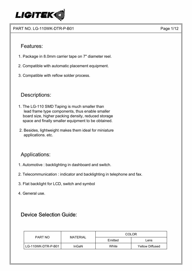
Device Selection Guide:
Device Selection Guide:
Features: 1. Package in 8.0mm carrier tape on 7" diameter reel.
2. Compatible with automatic placement equipment.
3. Compatible with reflow solder process.
Descriptions:
1. The LG-110 SMD Taping is much smaller than lead frame type components, thus enable smaller board size, higher packing density, reduced storage space and finally smaller equipment to be obtained.
2. Besides, lightweight makes them ideal for miniature applications. etc.
Applications: 1. Automotive : backlighting in dashboard and switch.
2. Telecommunication : indicator and backlighting in telephone and fax.
3. Flat backlight for LCD, switch and symbol
4. General use.
PART NO. LG-110WK-DTR-P-B01 Page 1/12

Package Dimensions
Note : The tolerances unless mentioned is ±0.1mm,Angle ±0.5. Unit=mm.
LIGITEK ELECTRONICS CO.,LTD.Property of Ligitek Only
Page 2/12 PART NO. LG-110WK-DTR-P-B01
Note : 1.All dimension are in millimeter tolerance is ±0.1mm unless otherwise noted. 2.Specifications are subject to change without notice.
Recommended Soldering Pad Dimensions
Package Dimensions
PCBR1.0
1.0
LED DICE
3.2
1.5
0.65
Soldering Terminal 0.8
0.65
Resin
0.5 Cathode Mark
0.9 1.0
5.0
1.0
1.5 1.5
1.0
0.5
1
2
3
1
2
1 23
1
2
3 NC
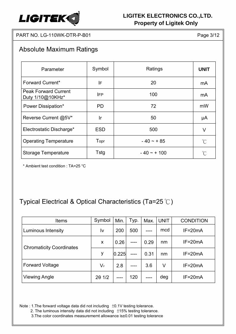
y 0.225 0.31---- nm IF=20mA Chromaticity Coordinates
x 0.26 nm0.29---- IF=20mA
Typical Electrical & Optical Characteristics (Ta=25℃)
UNIT CONDITIONSymbolItems Typ.Min. Max.
----
3.6
---- Viewing Angle
Forward Voltage
Luminous Intensity
VF
2θ 1/2
----2.8
---- 120
Iv 500200
V
deg
IF=20mA
IF=20mA
mcd IF=20mA
LIGITEK ELECTRONICS CO.,LTD.Property of Ligitek Only
Page 3/12 PART NO. LG-110WK-DTR-P-B01
Absolute Maximum Ratings
Power Dissipation*
Forward Current*
Electrostatic Discharge*
Operating Temperature
Reverse Current @5V*
Peak Forward Current Duty 1/10@10KHz*
Storage Temperature
- 40 ~ + 85Topr
Tstg - 40 ~ + 100
Symbol
PD
IFP
ESD
Ir
IF
Parameter
50
500
20
72
100
Ratings
℃
℃
mA
μA
V
UNIT
mW
mA
* Ambient test condition : TA=25 °C
Note : 1.The forward voltage data did not including ±0.1V testing tolerance. 2. The luminous intensity data did not including ±15% testing tolerance.
3.The color coordinates measurememt allowance is±0.01 testing tolerance
LIGITEK ELECTRONICS CO.,LTD.Property of Ligitek Only
Page 4/12
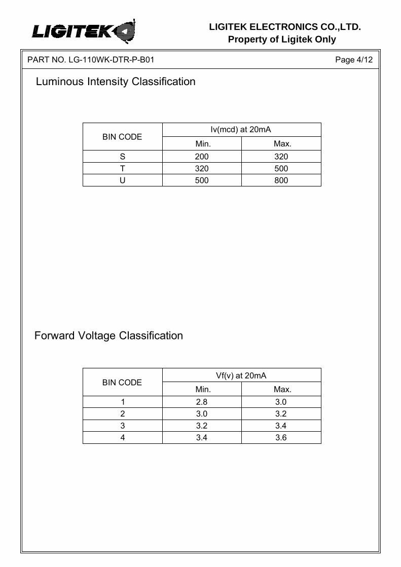
Luminous Intensity Classification
Forward Voltage Classification
Vf(v) at 20mA
Min.
4
23
1
3.43.2
2.83.0
BIN CODEMax.
3.2
3.63.4
3.0
Iv(mcd) at 20mABIN CODE
Min. Max.
500320
UT
800500
200S 320
PART NO. LG-110WK-DTR-P-B01

Page 5/12
LIGITEK ELECTRONICS CO.,LTD.Property of Ligitek Only
PART NO. LG-110WK-DTR-P-B01
. CIE Chromaticity Diagram
. Chromaticity Coordinates Specifications for Bin Grading
Color Coordiante at20mA
x yBIN CODE
1 32 4
0.14
0.16
0.18
0.20
0.22
0.24
0.26
0.28
0.30
0.32
0.34
0.36
0.38
0.40
0.42
0.20 0.22 0.24 0.26 0.28 0.30 0.32 0.34 0.36
B1
B2
B3
0.26B1 0.26 0.265 0.270.225 0.24 0.27 0.28
0.27B2 0.27 0.28 0.280.24 0.225 0.28 0.295
0.28B3 0.28 0.295 0.290.255 0.27 0.29 0.31
x y x y x y

Typical Electro-Optical Characteristics Curve
LIGITEK ELECTRONICS CO.,LTD.Property of Ligitek Only
WK CHIP
PART NO. LG-110WK-DTR-P-B01 Page 6/12
Fig.5 Luminous Spectrum(Ta=25 ℃)
Inte
nsity
Wavelength (nm)
0.5
Rel
ativ
e In
tens
ity@
20m
AN
orm
aliz
e @
25℃
20
Ambient Temperature( ℃)
0-40 -20
0.0
60 1008040
Fig.4 Relative Intensity vs. Temperature
2.5
1.5
1.0
2.0
3.0
Rel
ativ
e In
tens
ityN
orm
aliz
e @
20m
A
Forward Current(mA)
1 10
0.0
0.5
1.0
1.5
2.0
100 1000
Fig.2 Relative Intensity vs. Forward Current
2.5
3.0
SPECTRAL RADIANCE
80
400 500 600
40
20
60
100
700 800 0
Fig.6 Directive Radiation
For
war
d C
urre
nt(m
A)
Forward Voltage(V)
Fig.1 Forward current vs. Forward Voltage
2.0
100
1.0
0.1
10
1.0
1000
3.0 4.0 5.0
0
10
20
30
40
0 20 40 60 80 100
Forw
ard
Cur
rent
(mA
)
Ambient Temperature (Ta°C)
Fig.3 Forward Current vs. Temperature

8.0mm tape,7"reel
Part No.
LG-110WK-DTR-P-B01
Quantity/ReelDescription
3000 devices
Note : The tolerances unless mentioned is ±0.1mm,Angle± 0.5. Unit=mm.
Packing Specifications‧
Carrier Tape Dimensions
PART NO. LG-110WK-DTR-P-B01
LIGITEK ELECTRONICS CO.,LTD.Property of Ligitek Only
Page 7/12
0.25
1.25
8.0±0.3
1.874.0±0.2
3.5±0.2
Polarity
1.75
4.0±0.2 1.52.0
5.3 3.4
LabelLabel Aluminum Moist-Proof bag

Label Explanation
Reel Dimensions
0.6
0.8
ψ13.5±1.0
178±1.5
12.0±1.09.0±1.0
2.0±0.5
0.2
0.4
0.6
0.2
0.4 0.8
6.0±1.0
Page 8/12 PART NO. LG-110WK-DTR-P-B01
LIGITEK ELECTRONICS CO., LTD.
VF:3.0-3.2 BIN/HUE : S/B2
QTY(PCS):
LOT :
PART :
Pb LG-110WK-DTR-P-B01
GS11730168
3000
VF : Forward Voltage
(CIE_x , CIE_y) HUE : Chromaticity Coordinates
BIN : Luminous Intensity
LIGITEK ELECTRONICS CO.,LTD.Property of Ligitek Only

LIGITEK ELECTRONICS CO.,LTD.Property of Ligitek Only
Page 9/12 PART NO. LG-110WK-DTR-P-B01
W
L
H
Box Explanation 1. 5 BAG / INNER BOX
2. INNER BOX SIZE : L X W X H 23cm X 8.5cm x 26cm
3. 10 INNER BOXES / CARTON
4. CARTON SIZE : L X W X H 58cm X 34cm x 35cm
LW
H

LIGITEK ELECTRONICS CO.,LTD.Property of Ligitek Only
Page 10/12 PART NO. LG-110WK-DTR-P-B01
Recommended Soldering Conditions
1. Hand Solder Basic spec is 280 3 sec one time only. ≦ ℃
3.After soldering,do not warp the circuit board.
Note:1.Reflow soldering should not be done more than two times.2.When soldering,do not put stress on the LEDs during heating.
120 sec.Max.
Preheat180~200°C
2 PB-Free Reflow Solder
1~5°C/sec
260°C MaX. 10sec.Max
Above 220°C 60 sec.Max.
1~5°C/sec
6°C/sec
LIGITEK ELECTRONICS CO.,LTD.Property of Ligitek Only
Page 11/12 PART NO. LG-110WK-DTR-P-B01
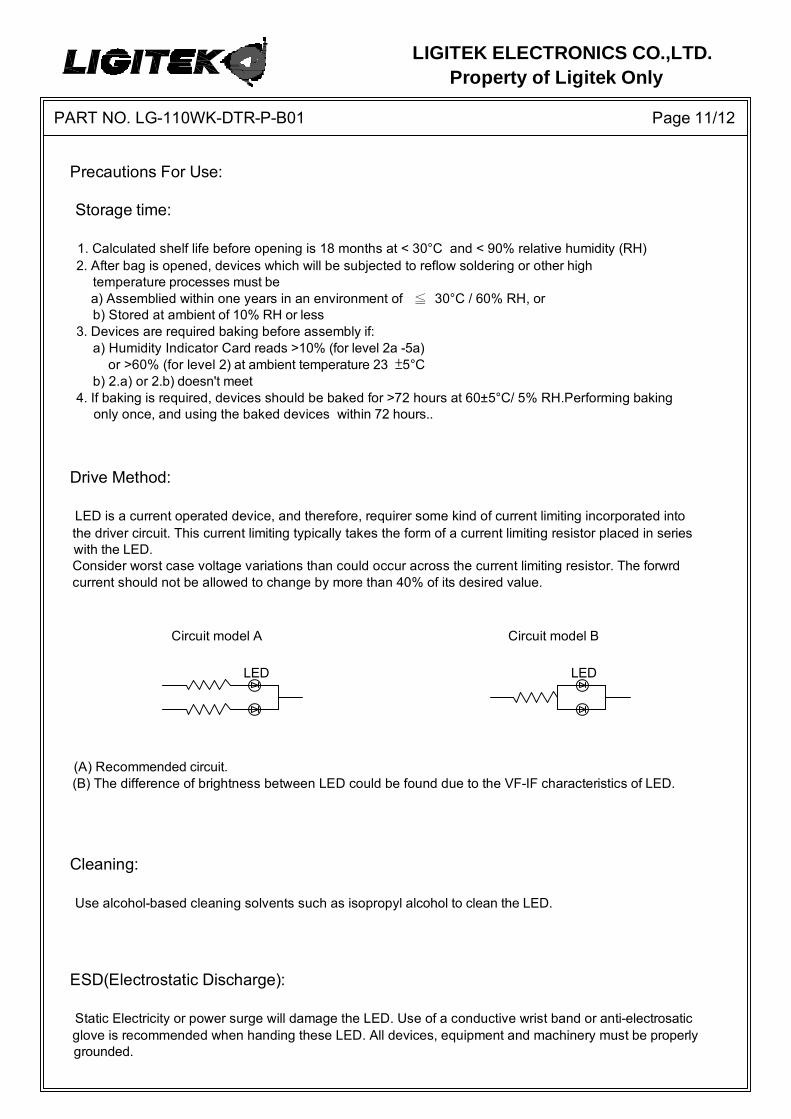
ESD(Electrostatic Discharge):
Static Electricity or power surge will damage the LED. Use of a conductive wrist band or anti-electrosatic glove is recommended when handing these LED. All devices, equipment and machinery must be properly grounded.
Cleaning:
Use alcohol-based cleaning solvents such as isopropyl alcohol to clean the LED.
(A) Recommended circuit. (B) The difference of brightness between LED could be found due to the VF-IF characteristics of LED.
Drive Method: LED is a current operated device, and therefore, requirer some kind of current limiting incorporated into the driver circuit. This current limiting typically takes the form of a current limiting resistor placed in series with the LED. Consider worst case voltage variations than could occur across the current limiting resistor. The forwrd current should not be allowed to change by more than 40% of its desired value.
Circuit model A
LED
Circuit model B
LED
Precautions For Use:
Storage time:
1. Calculated shelf life before opening is 18 months at < 30°C and < 90% relative humidity (RH) 2. After bag is opened, devices which will be subjected to reflow soldering or other high temperature processes must be a) Assemblied within one years in an environment of ≦ 30°C / 60% RH, or b) Stored at ambient of 10% RH or less 3. Devices are required baking before assembly if: a) Humidity Indicator Card reads >10% (for level 2a -5a) or >60% (for level 2) at ambient temperature 23 ±5°C b) 2.a) or 2.b) doesn't meet 4. If baking is required, devices should be baked for >72 hours at 60±5°C/ 5% RH.Performing baking
only once, and using the baked devices within 72 hours..

LIGITEK ELECTRONICS CO.,LTD.Property of Ligitek Only
Page 12/12 PART NO. LG-110WK-DTR-P-B01
Reliability Test:
EnvironmentalTest
1.T=260°C Max. 10sec.Max. 2. 6 Min
IR Reflow
1.100°C±5°C ~ -40°C±5°C 30mins / 5mins / 30mins 2.100 Cyeles
TemperatureCycling
EnduranceTest
Classification
1.Ta=85°C 2.RH=85% 3.t=1000hrs(-24hrs,+72hrs)
1.Ta=-40°C±5°C 2.t=1000 hrs (-24hrs,+72hrs)
1.Ta=100°C±5°C ~ -40°C±5°C 20min/ 10sec / 20min 2.total 100 cycles
High Temperature High Humidity Storage Test
Thermal Shock Test
Low Temperature Storage Test
1.Ta=100°C±5°C 2.t=1000 hrs (-24hrs,+72hrs)
1.Ta=25°C 2.If=20mA 3.t=1000 hrs (-24hrs,+72hrs)
High Temperature Storage Test
Test Item
Operating Life Test
Test Condition SampleSize
22
22
22
22
22
22
22