datasheet search site | transmitter...digital fm transmitter, is designed to process high-fidelity...
TRANSCRIPT

KT0803K
Monolithic Digital Stereo FM Transmitter Radio-Station-on-a-Chip™
Features Hardware compatible with KT0803 Additional features to KT0803
Increased transmission Power Input signal detection Bass boost control 32.768 KHz clock support
Professional Grade Performance: SNR ≥ 60 dB Stereo Separation > 40 dB International compatible 70MHz ~ 108MHz
Ultra-Low Power Consumption: < 17 mA operation current < 3 µA standby current
Small Form factor: 16-pin SOP
Simple Interface: Single power supply Industry standard 2-wire I2C MCU interface compatible
Advanced Digital Audio Signal Processing: On-chip 20-bit ΔΣ Audio ADC On-chip DSP core On-chip 24dB PGA with optional 1dB stepAutomatic calibration against process and temperature
On-Chip LDO (low-drop-out) regulator: Accommodates 1.6V ~ 3.6V supply
Programmable transmit level Programmable pre-emphasis (50/75 µs) Pb-free and RoHS Compliant
Applications MP3 Player Cellular Phone PDA Portable Personal Media player Laptop Computer Wireless Speaker
Rev. 1.1 Information furnished by KT Micro is believed to be accurate and reliable. However, no responsibility is assumed by KT Micro for its use, nor for any infringements of patents or other rights of third parties which may result from its use. No license is granted by implication or otherwise under any patent or patent rights of KT Micro, Inc..
Figure 1: KT0803K System Diagram
General Description KT0803K, our new generation of low cost Monolithic Digital FM Transmitter, is designed to process high-fidelity stereo audio signal and transmit modulated FM signal over a short range. It’s based on the architecture of award-winning KT0801 and it’s also an upgrade of KT0803. The additional features added to KT0803K are increased transmission power up to 113 dBuV, auto level detection and bass boost and support of 32.768K Hz clock or crystal. The KT0803K features dual 20-bit ΔΣ audio ADCs, a high-fidelity digital stereo audio processor and a fully integrated radio frequency (RF) transmitter. An on-chip low-drop-out regulator (LDO) allows the chip to be integrated in a wide range of low-voltage battery-operated systems with power supply ranging from 1.6V to 3.6V. The KT0803K is configured as an I2C slave and programmed through the industry standard 2-wire MCU interface. Thanks to its high integration level, the KT0803K is mounted in a generic 16-pin SOP package. It only requires a single low-voltage supply. No external tuning is required that makes design-in effort minimum. KT Micro Inc., 22391 Gilberto, Suite D Rancho Santa Margarita, CA 92688 Tel: 949.713.4000 http://www.ktmicro.com Fax: 949.713.4004 Copyright ©2009, KT Micro, Inc..

Copyright ©2009, KT Micro, Inc. 2
KT0803K
Operation Condition Table 1: Operation Condition
Parameter Symbol Operating Condition Min Typ Max Units 1.8V Analog Supply1 VDD Relative to GND 1.6 1.8 2.0 V IO/Regulator Supply IOVDD Relative to GND 1.6 3.6 V Operating Temp TA Ambient Temperature 0 25 70 °C Note: 1. No external voltage should be applied to this supply. Decoupling cap should be used instead
Specifications and Features Table 2: FM Transmitter Functional Parameters (Unless otherwise noted TA = 0-70 oC,
IOVDD=1.6~3.6 V, Fin = 1 kHz) Parameter Symbol Test/Operating
Condition Min Nom Max Units
FM Frequency Range Ftx Pin 16 76 108 MHzCurrent Consumption IVDD Pin 4 with PA (power
amp.) at default power mode (PA_bias = 0, RFGAIN[3:0]=1111)
- 17 mA
Standby Current Istand Pin 4 - 0.1 1 μA Signal to Noise Ratio SNR Vin = 0.7 Vp-p, Gin = 0 - 60 - dB Total Harmonic Distortion THD Vin = 0.7 Vp-p, Gin = 0 - 0.3 % Left/Right Channel Balance BAL Vin = 0.7 Vp-p, Gin = 0 -0.2 - 0.2 dB Stereo Separation (Left<->Right) SEP Vin = 0.7 Vp-p, Gin = 0 40 - dB Sub Carrier Rejection Ratio SCR Vin = 0.7 Vp-p, Gin = 0 - - 60 dB Input Swing1 Vin Single-ended input - 0.35 1.4 VRMS
PGA Range for Audio Input Gin -12 0 12 dB PGA Gain Step for Audio Input Gstep 1 4 dB Required Input Common-Mode Voltage when DC-coupled
Vcm Pin 5,7 0 0.8 1.8 V
Power Supply Rejection2 PSRR IOVDD = 1.9 ~ 3.6 V 40 - - dB Ground Bounce Rejection2 GSRR IOVDD = 1.9 ~ 3.6 V 40 - - dB Input Resistance (Audio Input) Rin Pin 5, 7 120 150 180 kΩ Input Capacitance (Audio Input) Cin Pin 5, 7 0.5 0.8 1.2 pF Audio Input Frequency Band Fin Pin 5, 7 20 - 15k Hz Transmit Level Vout 96 103 113 dBµVChannel Step STEP - 50 kHz Pilot Deviation 7.5 15 kHz Audio Deviation 75 150 kHz Frequency Response Mono,-3dB, ΔF=60kHz,
50/75μs pre-emphasis 30 15k Hz
SIG_PROC<1> = 1 - 50 - µs Pre-emphasis Time Constant Tpre SIG_PROC<0> = 0 - 75 - µs
Crystal/External Clock CLK Input clock 32.768 KHz2-wire I2C Clock SCL Pin 14 0 100 400 kHz High Level Input Voltage VIH Pin 4, 8, 12, 14, 16 0.75 x
IOVDD - IOVDD + 0.25 V
Low Level Input Voltage VIL Pin 4, 8, 12, 14, 16 - 0.25 - 0.25 x IOVDD V

Copyright ©2009, KT Micro, Inc. 3
KT0803K
Notes: 1. Maximum is given on the condition of PGA gain = -12dB. 2. Fin = 20 ~ 15k Hz.
Package and Pin List
Table 3: KT0803K Pin Definition Pin Index Name I/O Type Function 2 XI Analog I/O Crystal input. 3 XO Analog I/O Crystal input 4 IOVDD Power 1.6~3.3V external logic IOVDD 1, 5,11,15 GND Ground Can be shorted together and connected to ground 6 INL Analog Input Left channel audio input. 7 INR Analog Input Right channel audio input. 8 SW Digital Input Control bit. Chip enable, supply mode 9, 12 GND Ground Ground 10 RSTB Digital Input Reset (active low). 13 SDA Digital I/O Serial data I/O. 14 SCL Digital I/O Serial clock input. 16 PA_OUT Analog Output FM RF output.
1
2
3
4
5
6
16
15
14
13
12
11
GNDXI
XOIOVDD
GNDINLINRSW
PA_OUT GND SCL SDA GND GND RSTB GND
KT
0803
K
7
8
10
9
Figure 2: KT0803K Pin-out

Copyright ©2009, KT Micro, Inc. 4
KT0803K
I2C Compatible 2-Wire Serial Interface
General Descriptions The serial interface consists of a serial controller and registers. An internal address decoder transfers the content of the data into appropriate registers. Please note that the I2C address is 0x 0111110 the same as in KT0803. Neither software nor hardware change is needed if KT0803K is used to replace KT0803.
Both the write and read operations are supported according to the following protocol:
Write Operations: BYTE WRITE: The write operation is accomplished via a 3-byte sequence: Serial address with write command Register address Register data A write operation requires an 8-bit register address following the device address word and acknowledgment. Upon receipt of this address, the KT0803K will again respond with a “0” and then clock in the 8-bit register data. Following receipt of the 8-bit register data, the KT0803K will output a “0” and the addressing device, such as a microcontroller, must terminate the write sequence with a stop condition (see Figure 3). Read Operations: RANDOM READ: The read operation is accomplished via a 4-byte sequence: Serial address with write command Register address Serial address with read command Register data Once the device address and register address are clocked in and acknowledged by the KT0803K, the microcontroller must generate another start condition. The microcontroller now initiates a current address read by sending a device address with the read/write select bit high. The KT0803K acknowledges the device address and serially clocks out the register data. The microcontroller does not respond with a “0” but does generate a following stop condition (see Figure 3). RANDOM REGISTER WRITE PROCEDURE S 0 1 1 1 1 1 0 W A A A P 7 bit address register address data Acknowledge Acknowledge STOP condition START condition WRITE command Acknowledge RANDOM REGISTER READ PROCEDURE S 0 1 1 1 1 1 0 W A A S 0 1 1 1 1 1 0 R A A P 7 bit address register address 7 bit address data Acknowledge Acknowledge Acknowledge START condition WRITE command READ condition NO Acknowledge STOP condition
Figure 3: Serial Interface Protocol
CURRENT ADDRESS READ: The internal data register address counter maintains the last address
Copyright ©2009, KT Micro, Inc. 5
KT0803K
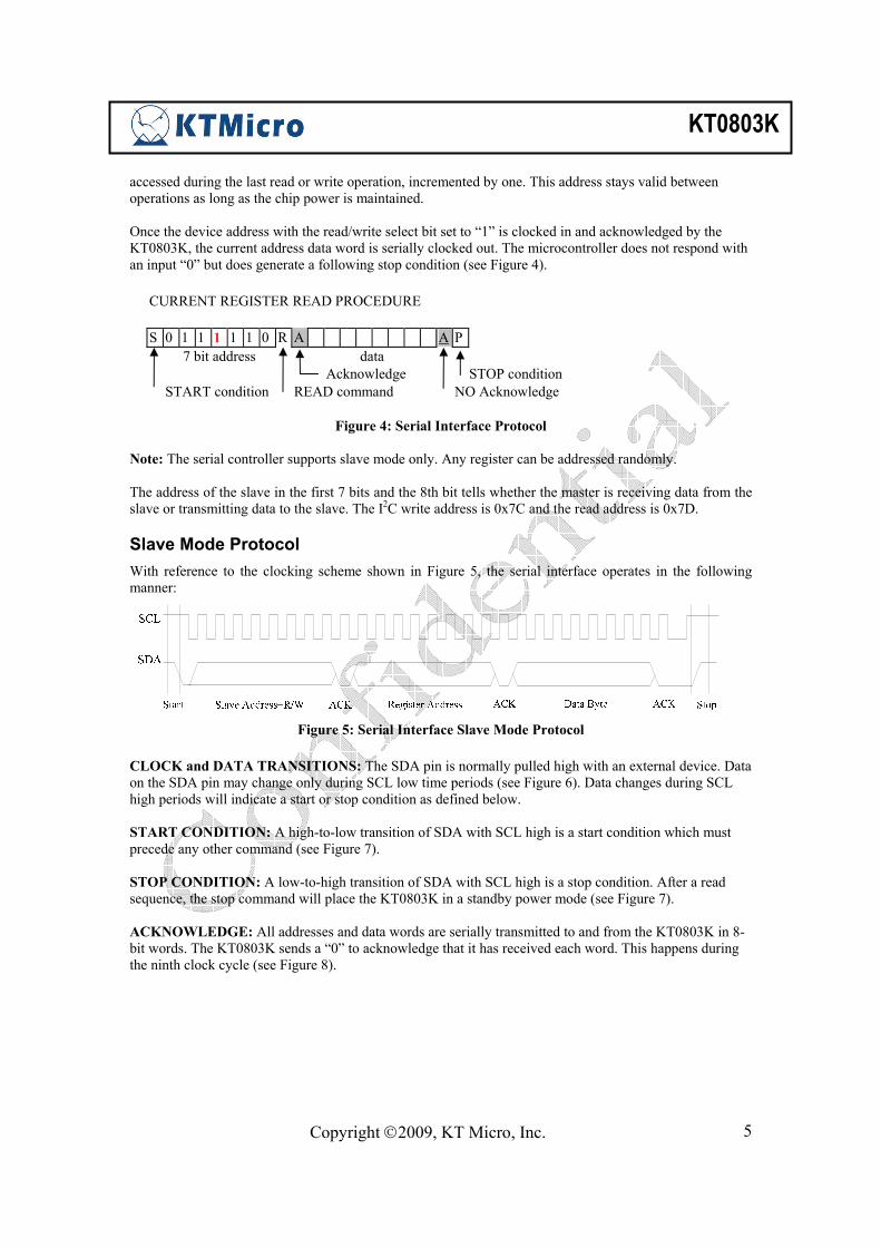
accessed during the last read or write operation, incremented by one. This address stays valid between operations as long as the chip power is maintained. Once the device address with the read/write select bit set to “1” is clocked in and acknowledged by the KT0803K, the current address data word is serially clocked out. The microcontroller does not respond with an input “0” but does generate a following stop condition (see Figure 4). CURRENT REGISTER READ PROCEDURE S 0 1 1 1 1 1 0 R A A P 7 bit address data Acknowledge STOP condition START condition READ command NO Acknowledge
Figure 4: Serial Interface Protocol
Note: The serial controller supports slave mode only. Any register can be addressed randomly. The address of the slave in the first 7 bits and the 8th bit tells whether the master is receiving data from the slave or transmitting data to the slave. The I2C write address is 0x7C and the read address is 0x7D.
Slave Mode Protocol With reference to the clocking scheme shown in Figure 5, the serial interface operates in the following manner:
Figure 5: Serial Interface Slave Mode Protocol
CLOCK and DATA TRANSITIONS: The SDA pin is normally pulled high with an external device. Data on the SDA pin may change only during SCL low time periods (see Figure 6). Data changes during SCL high periods will indicate a start or stop condition as defined below. START CONDITION: A high-to-low transition of SDA with SCL high is a start condition which must precede any other command (see Figure 7). STOP CONDITION: A low-to-high transition of SDA with SCL high is a stop condition. After a read sequence, the stop command will place the KT0803K in a standby power mode (see Figure 7). ACKNOWLEDGE: All addresses and data words are serially transmitted to and from the KT0803K in 8-bit words. The KT0803K sends a “0” to acknowledge that it has received each word. This happens during the ninth clock cycle (see Figure 8).

Copyright ©2009, KT Micro, Inc. 6
KT0803K
Figure 6: Clock and Data Transitions
Figure 7: Start and Stop Definition
Figure 8: Acknowledge

Copyright ©2009, KT Micro, Inc. 7
KT0803K
Register Bank The register bank stores channel frequency codes, calibration parameters, operation status, mode and power controls, which can be accessed by the internal digital controller, state machines and external micro controllers through the serial interface.
All registers are 8 bits wide. Control logics are active high unless specifically noted. Register 7 6 5 4 3 2 1 0
0x00 CHSEL[8:1] 0x01 RFGAIN[1:0] PGA[2:0] CHSEL[11:9] 0x02 CHSEL[0] RFGAIN[3] - - MUTE PLTADJ - PHTCNST0x04 MONO PGA_LSB[1:0] FDEV[1:0] BASS[1:0] 0x0B - - PDPA - - - - - 0x0E - - - - - - PA_BIAS - 0x0F - - - PW_OK - SLNCID - - 0x10 - - - LMTLVL[1:0] - - PGAMOD0x12 SLNCDIS SLNCTHL[2:0] SLNCTHH[2:0] SW_MOD0x13 RFGAIN[2] - - - - PA_CTRL - - 0x14 SLNCTIME[2:0] SLNCCNTHIGH[2:0] - - 0x16 - - - SLNCCNTLOW[2:0]
Note 1: ONLY read/write the defined registers.
Note 2: Shaded registers are used in KT0803.
Register 0x00 (Address: 0x00, Default value: 0x81) Bit 7 6 5 4 3 2 1 0
KT0803K CHSEL[8:1] KT0803 CHSEL[7:0]
As the minimum frequency step is changed from 100KHz in KT0803 to 50KHz in KT0803K. The 12 bits (Reg0x1[2:0]; Reg0x0[7:0]; Reg0x2[7]) are required to select the FM transmission channel instead of 11 bits in KT0803. If a 100 KHz step is wanted, set Reg0x2[7] to 0 and thus no software change is needed from KT0803 to KT0803K to set the same FM frequency.
Register 0x01 (Address: 0x01, Default value: 0xC3) Bit 7 6 5 4 3 2 1 0
KT0803K RFGAIN[1:0] PGA[2:0] CHSEL[11:9] KT0803 RFGAIN[1:0] PGA[2:0] CHSEL[10:8]
Bits Type Default Label Description 7:6 RW 11 RFGAIN[1:0] Transmission Range Adjustment with RFGAIN[3] in Reg
0x02[6] and RFGAIN[2] in Reg 0x13[7] (See Table 4 below)
5:3 RW 000 PGA[2:0] PGA Gain Control (see PGA_LSB description, Reg 0x04) 111: 12dB 110: 8dB 101: 4dB 100: 0dB 000: 0dB 001: -4dB 010: -8dB 011: -12dB
2:0 RW 011 CHSEL[11:9] FM Channel Selection[11:9]

Copyright ©2009, KT Micro, Inc. 8
KT0803K
Table 4: Transmission power setting
RFGAIN<3:0> RFOUT 0000 95.5 dBuV 0001 96.5 dBuV 0010 97.5 dBuV 0011 98.2 dBuV 0100 98.9 dBuV 0101 100 dBuV 0110 101.5 dBuV 0111 102.8 dBuV 1000 105.1 dBuV (107.2dBuV PA_BIAS=1) 1001 105.6 dBuV (108dBuV, PA_BIAS=1) 1010 106.2 dBuV (108.7dBuV, PA_BIAS=1) 1011 106.5 dBuV (109.5dBuV, PA_BIAS=1) 1100 107 dBuV (110.3dBuV, PA_BIAS=1) 1101 107.4 dBuV (111dBuV, PA_BIAS=1) 1110 107.7 dBuV (111.7dBuV, PA_BIAS=1) 1111 (default setting) 108 dBuV (112.5dBuV, PA_BIAS=1)
Register 0x02 (Address: 0x02, Default: 0x40) Bit 7 6 5 4 3 2 1 0
KT0803K CHSEL[0] RFGAIN[3] - - MUTE PLTADJ - PHTCNSTKT0803 - - - - MUTE PLTADJ - PHTCNST
Bits Type Default Label Description 7 RW 0 CHSEL[0] LSB o CHSEL, additional to KT0803 6 RW 1 RFGAIN[3] MSB of RFGAIN 5:4 RW 00 Reserved 3 RW 0 MUTE Software Mute
1: MUTE Enabled 0: MUTE Disabled
2 RW 0 PLTADJ Pilot Tone Amplitude Adjustment 1: Amplitude high 0: Amplitude low
1 RW 0 NA Reserved 0 RW 0 PHTCNST Pre-emphasis Time-Constant Set
1: 50 μs (Europe, Australia) 0: 75 μs (USA, Japan)
Register 0x04 (Address: 0x04, Default: 0x04) - New Bit 7 6 5 4 3 2 1 0
KT0803K - MONO PGA_LSB[1:0] FDEV[1:0] BASS[1:0] KT0803 - - - - -
Bits Type Default Label Description 7 RW 0 Reserved 6 RW 0 MONO Force MONO

Copyright ©2009, KT Micro, Inc. 9
KT0803K
Bits Type Default Label Description 5:4 RW 00 PGA_LSB[1:0] PGA<2:0> PGA_LSB<1:0> PGA Gain
111 11 12dB 111 10 11 111 01 10 111 00 9 110 11 8 110 10 7 110 01 6 110 00 5 101 11 4 101 10 3 101 01 2 101 00 1 100 11 0 100 10 0 100 01 0 100 00 0 000 00 0 000 01 -1 000 10 -2 000 11 -3 001 00 -4 001 01 -5 001 10 -6 001 11 -7 010 00 -8 010 01 -9 010 10 -10 010 11 -11 011 00 -12 011 01 -13 011 10 -14 011 11 -15
3:2 RW 01 FDEV[1:0] Frequency deviation adjustment 00 : 75kHz 01 : 112.5kHz 10 : 150kHz 11 : 187.5kHz
1:0 RW 00 BASS[1:0] Bass boost control 00 :Disabled 01 : 5dB 10 : 11dB 11 : 17dB
Register 0x0B (Address: 0x0B, Default: 0x00) - New Bit 7 6 5 4 3 2 1 0
KT0803K - - PDPA - - - - - KT0803 - - - - - - - -
Bits Type Default Label Description 7 RW 0 Reserved

Copyright ©2009, KT Micro, Inc. 10
KT0803K
Bits Type Default Label Description 6 RW 0 Reserved 5 RW 0 PDPA Power Amplifier Power Down 4 RW 0 Reserved 3 RW 0 Reserved 1 RW 0 Reserved 0 RW 0 Reserved
Register 0x0E (Address: 0x0E, Default: 0x02) – New Bit 7 6 5 4 3 2 1 0
KT0803K - - - - - - PA_BIAS - KT0803 - - - - - - - -
Bits Type Default Label Description 7:2 RW 0x00 Reserved 1 RW 1 PA_BIAS PA bias current enhancement. 0 RW 0 Reserved
Register 0x0F (Address: 0x0F, Read only) – New Bit 7 6 5 4 3 2 1 0
KT0803K - - - PW_OK - SLNCID - - KT0803 - - - - - - - -
Bits Type Default Label Description 7 R NA Reserved 6 R NA Reserved 5 R NA Reserved 4 R NA PW_OK Power OK indicator 3 R NA Reserved 2 R NA SLNCID 1 when Silence is detected 1 R NA Reserved 0 R NA Reserved
Register 0x10 (Address: 0x10, Default: 0x08) – New Bit 7 6 5 4 3 2 1 0
KT0803K - - - LMTLVL[1:0] - - PGAMODKT0803 - - - - - - - -
Bits Type Default Label Description 7:5 RW 000 Reserved 4:3 RW 01 LMTLVL[1:0] Internal audio limiter level control
00 = 0.6875 01 = 0.75 10 = 0.875 11 = 0.9625
2:1 RW 00 Reserved 0 RW 0 PGAMOD PGA mode selection
0 = 4dB step (compatible with KT0803) 1 = 1dB step with PGA_LSB[1:0 ] used

Copyright ©2009, KT Micro, Inc. 11
KT0803K
Register 0x12 (Address: 0x12, Default: 0x80) - New Bit 7 6 5 4 3 2 1 0
KT0803K SLNCDIS SLNCTHL[2:0] SLNCTHH[2:0] SW_MODKT0803 - - - - - - - -
Bits Type Default Label Description 7 RW 1 SLNCDIS Silence detection disable
0 : enable 1 : disable
6:4 RW 000 SLNCTHL Silence detection low threshold 000 : 0.25mv 001 : 0.5mv 010 : 1mv 011 : 2mv 100 : 4mv 101 : 8mv 110 : 16mv 111 : 32mv
3:1 RW 000 SLNCTHH Silence detection high threshold 000 : 0.5mv 001 : 1mv 010 : 2mv 011 : 4mv 100 : 8mv 101 : 16mv 110 : 32mv 111 : 64mv
0 RW 0 SW_MOD Switching channel mode selection. 0 = mute when changing channel 1 = pa off when changing channel
Register 0x13 (Address: 0x13, Default: 0x80) Bit 7 6 5 4 3 2 1 0
KT0803K RFGAIN[2] - - PA_CTRL - - KT0803 PA_HI_PW - - - - - - -
Bits Type Default Label Description 7 RW 1 RFGAIN[2] PA (Power amplifier) power (combined with Reg
0x01[7:6] and Reg 0x02[6])to set up transmission range)
6:3 RW 0000 Reserved 2 RW 0 PA_CTRL Power amplifier structure selection
0 = Internal power supply, KT0803 compatible 1 = External power supply via external inductor Note : When an external inductor is used, this bit must be set to 1 immediately after the Power OK indicator Reg 0x0F[4] is set to 1. Otherwise, the device may be destroyed!
1:0 RW 00 Reserved

Copyright ©2009, KT Micro, Inc. 12
KT0803K
Register 0x14 (Address: 0x14, default 0x00) - New Bit 7 6 5 4 3 2 1 0
KT0803K SLNCTIME<2:0> SLNCCNTHIGH<2:0> - - KT0803 - - - - - - - -
Bits Type Default Label Description 7:5 RW 000 SLNCTIME<2:0> Silence detection low level and high level duration
time 000 : 50ms 001 : 100ms 010 : 200ms 011 : 400ms 100 : 1s 101 : 2s 110 : 4s 111 : 8s
4:2 RW 000 SLNCCNTHIGH<2:0>
Silence detection high level counter threshold 000 : 15 001 : 31 010 : 63 011 : 127 100 : 255 101 : 511 110 : 1023 111 : 2047
1:0 RW 00 Reserved
Register 0x16 (Address 0x16, default: 0x00) - New Bit 7 6 5 4 3 2 1 0
KT0803K - - - SLNCCNTLOW[2:0] KT0803 - - - - - - - -
Bits Type Default Label Description 7:3 RW 0x0 Reserved 2:0 RW 000 SLNCCNTLOW[2:0] Silence low counter
000 : 1 001 : 2 010 : 4 011 : 8 100 : 16 101 : 32 110 : 64 111 : 128
Copyright ©2009, KT Micro, Inc. 13
KT0803K
Chip Enable and Mode Control There is one external pin SW (Pin 8) to enable the chip. The definition is shown below.
Table 5: Pin SW
Input SW Chip Mode IOVDD Clock Source
0 Power off N/A N/A 1 Power On 1.6~3.6V External crystal or clock
Mute The FM transmitter can be muted by setting Register MUTE to “1” through I2C programming.
Silence Detection Bit name Register location Description SLNCDIS Reg 0x12[7] Setting to 0 to enable the silence detection SLNCTIME[2:0] Reg 0x14[7:5] silence detection time window SLNCTHL[2:0] Reg 0x12[6:4] Low threshold voltage of input signal for silence detection SLNCTHH[2:0] Reg 0x12[3:1] High threshold voltage of input signal for silence detection SLNCCNTTHL[2:0] Reg 0x14[4:2] # of time when the input signal amplitude is lower than
SLNCTHL SLNCCNTTHH[2:0] Reg 0x16[2:1] # of time when the input signal amplitude is higher than
SLNCTHH SLNCID Reg 0x0F[2] (Read only) Set to 1 when silence is detected. The silence detection scheme is enabled by setting SLNCDIS to 0. During the time defined by SLNTIME[2:0], the chip will be muted when the number of time when the input amplitude is higher than the voltage defined by SLNCTHL[2:0] is lower than SLNCCNTTHL[2:0]. The SLNCID bit is set to 0. When the input signal amplitude is higher than the voltage defined by SLNCTHH[2:0] and the number of time when that happens is more than SLNCCNTTHH[2:0], the chip exits from the mute status and the SLNCID is cleared to 0.
Reset The global reset is issued after the RSTB pin set to “0” or automatic on-chip power-on reset. After a global reset, all registers are reset to the default value.

Copyright ©2009, KT Micro, Inc. 14
KT0803K
Typical Application Circuits The KT0803K can be integrated in a wide range of systems by requiring only a single power supply. Figure 9 shows the external diagram for the drop-in replacement of KT0803.
Figure 9: Typical configuration for a drop-in replacement
As shown in the red block above, Pin 1, 5, 11 and 15 are VDD pins in KT0803 that are required to be connected to a decoupling capacitor. These four pins are GND pins in KT0803K. Customers can replace the decoupling capacitor of a 0-ohm resister without PCB board change.
KT0803K
SDA SCL
INL
INR
Stereo Audio Line Input
Pin 1,5,11,15 GND
RSTB SW
PA_OUT
Antenna
32.768 KHz XTAL
33nF
33nF
XI XO
3.3V
IOVDD
Optional
MCU (3.3 V CMOS Logic)
I2C POR On/Off
HF
0ΩKT0803K
3 3VKT0803
Pin 1,5,11,15

Copyright ©2009, KT Micro, Inc. 15
KT0803K
Figure 10: Application that requires higher transmission power (>5dBm)
KT0803K
SDA SCL
INL
INR
Stereo Audio Line Input
Pin 1,5,11,15 GND
RSTB SW
PA_OUT
Antenna
32.768 KHz
33nF
33nF
XI XO
3.3V
IOVDD
Optional
MCU (3.3 V CMOS Logic)
I2C POR On/Off

Copyright ©2009, KT Micro, Inc. 16
KT0803K
Package Outline
(MILLIMETERS) (MILLIMETERS) Symbols MIN NOM MAX Symbols MIN NOM MAX A 1.75 D 9.70 9.90 10.10 A1 0.10 0.25 E 5.80 6.00 6.20 A2 1.30 1.40 1.50 E1 3.70 3.90 4.10 A3 0.60 0.65 0.70 e 1.27BSC b 0.39 0.48 h 0.25 0.50
b1 0.38 0.41 0.43 L 0.50 0.80 c 0.21 0.26 L1 1.05BSC
C1 0.19 0.20 0.21 θ 0 8°

Copyright ©2009, KT Micro, Inc. 17
KT0803K
Revision History V1.0 Official Release V1.1 I2C addresses in text

Copyright ©2009, KT Micro, Inc. 18
KT0803K
Contact Information KT Micro Inc. 22391 Gilberto, Suite D Rancho Santa Margarita, CA 92688 USA Tel: 949-713-4000 Fax: 949-713-4004 Email: [email protected] 北京昆腾微电子有限公司 北京市海淀区蓝靛厂东路 2 号金源时代商务中心 2 号楼 B 座 8 层 (100089) 电话:8610-88891945 传真:8610-88891977 电子邮件:[email protected] 网站:http://www.ktmicro.com.cn