datasheet - renesas electronics · datasheet the tw6865 is a highly integrated solution that...
TRANSCRIPT

FN8304Rev.1.00
Feb 15, 2016
TW68654-in-1 Video Decoders with PCI Express Media Bridge
DATASHEET
The TW6865 is a highly integrated solution that supports multi-channel video and audio capture via PCIe x1 interface for PC DVR system and video analytic application. It contains high quality four-channel NTSC/PAL/SECAM video decoders that convert analog composite video signal to digital component YCbCr data and utilize adaptive 4H comb filter for separating luminance and chrominance to reduce cross noise artifacts.
The TW6865 contains a high performance proprietary DMA controller that fully optimizes the utilization of PCIe x1 bandwidth and enables it to transfer video and audio data at a high throughput rate that closely approaches the theoretical limit of PCIe x1 interface. The TW6865 is able to simultaneously decode and transfer 4 real time D1 video, or up to 16-channel non-real time D1, plus 8-channel audio.
The TW6865 decreases the complexity and workload of client-side software development, and significantly reduces the strains on PC hardware and resources. TW6865 also includes a Software Development Kit (SDK) with Windows and Linux compliant drivers and reference application software.
Applications• PC-based DVR system
• Video analytic system
FeaturesVideo Decoders• Accepts all NTSC(M/N/4.43)/
PAL(B/D/G/H/I/K/L/M/N/60) standards with auto detection
• Integrated eight video analog anti-alias filters and 10-bit CMOS ADCs
• IF compensation filter for improvement of color demodulation
• Color Transient Improvement (CTI)
• White peak AGC control
• Programmable hue, saturation, contrast, brightness and sharpness
• High quality proprietary fast video locking system for non real time application
• High performance adaptive 4H comb filters for all NTSC and PAL standards
• Audio Codecs
• Integrated eight audio ADCs
• 8/16 bit audio word length
• Sample audio with 8/16/32/44.1/48kHz
DMA Controller• Highly-efficient DMA design can support up to 4 real time
D1 video and 8 real time audio channels, or up to 16 non-real time video with optimization of full PCIe x1 bandwidth
• Multiple video format output support: UYVY/Y422, YUYV/YUY2, IYU1/Y411, Y41P, YUV420, RGB555 and RGB565
• Integrated internal video and audio generator simplifies system test and development
• Built-in motion detection engine for each video channel
• Hardware-friendly design enables smooth data transfer and virtually eliminates unwanted big-block data jamming among PC devices, resulting in optimized PC internal bandwidth consumption
• PCIe configurations
• PCI Express Base Specification 1.1 Compliant
• Flexible PCIe packet size configuration: 128 byte, 256 byte and 512 byte options
TABLE 1. KEY DIFFERENCES BETWEEN FAMILY OF PARTS
PART NUMBERVIDEO
INPUTSAUDIO INPUTS
AMBIENT OPERATING
TEMPERATURE(°C)
TW6865-TA1-CR 4 8 0 to +70
TW6865-TA1-CRH 4 8 -40 to +85
TW6869-TA1-CR 8 8 0 to +70
TW6869-TA1-CRH 8 8 -40 to +85
FN8304 Rev.1.00 Page 1 of 77Feb 15, 2016

TW6865
Table of ContentsBlock Diagram . . . . . . . . . . . . . . . . . . . . . . . . . . . . . . . . . . . . . . . . . . . . . . . . . . . . . . . . . . . . . . . . . . . . . . . . . . . . . . . . . . . . . . . . . . . . . . 3
Pin Configuration. . . . . . . . . . . . . . . . . . . . . . . . . . . . . . . . . . . . . . . . . . . . . . . . . . . . . . . . . . . . . . . . . . . . . . . . . . . . . . . . . . . . . . . . . . . . 4
Pin Descriptions. . . . . . . . . . . . . . . . . . . . . . . . . . . . . . . . . . . . . . . . . . . . . . . . . . . . . . . . . . . . . . . . . . . . . . . . . . . . . . . . . . . . . . . . . . . . . 5
Ordering Information . . . . . . . . . . . . . . . . . . . . . . . . . . . . . . . . . . . . . . . . . . . . . . . . . . . . . . . . . . . . . . . . . . . . . . . . . . . . . . . . . . . . . . . . 6
Absolute Maximum Ratings . . . . . . . . . . . . . . . . . . . . . . . . . . . . . . . . . . . . . . . . . . . . . . . . . . . . . . . . . . . . . . . . . . . . . . . . . . . . . . . . . . . 7
Thermal Information . . . . . . . . . . . . . . . . . . . . . . . . . . . . . . . . . . . . . . . . . . . . . . . . . . . . . . . . . . . . . . . . . . . . . . . . . . . . . . . . . . . . . . . . . 7
Recommended Operating Conditions . . . . . . . . . . . . . . . . . . . . . . . . . . . . . . . . . . . . . . . . . . . . . . . . . . . . . . . . . . . . . . . . . . . . . . . . . . 7
Electrical Specifications . . . . . . . . . . . . . . . . . . . . . . . . . . . . . . . . . . . . . . . . . . . . . . . . . . . . . . . . . . . . . . . . . . . . . . . . . . . . . . . . . . . . . 7
Functional Description . . . . . . . . . . . . . . . . . . . . . . . . . . . . . . . . . . . . . . . . . . . . . . . . . . . . . . . . . . . . . . . . . . . . . . . . . . . . . . . . . . . . . . 10Video Decoder . . . . . . . . . . . . . . . . . . . . . . . . . . . . . . . . . . . . . . . . . . . . . . . . . . . . . . . . . . . . . . . . . . . . . . . . . . . . . . . . . . . . . . . . . . . . . . . . . . 10Color Decoding. . . . . . . . . . . . . . . . . . . . . . . . . . . . . . . . . . . . . . . . . . . . . . . . . . . . . . . . . . . . . . . . . . . . . . . . . . . . . . . . . . . . . . . . . . . . . . . . . . 14Chrominance Processing . . . . . . . . . . . . . . . . . . . . . . . . . . . . . . . . . . . . . . . . . . . . . . . . . . . . . . . . . . . . . . . . . . . . . . . . . . . . . . . . . . . . . . . . . 15Video Cropping . . . . . . . . . . . . . . . . . . . . . . . . . . . . . . . . . . . . . . . . . . . . . . . . . . . . . . . . . . . . . . . . . . . . . . . . . . . . . . . . . . . . . . . . . . . . . . . . . . 16Video Scaler . . . . . . . . . . . . . . . . . . . . . . . . . . . . . . . . . . . . . . . . . . . . . . . . . . . . . . . . . . . . . . . . . . . . . . . . . . . . . . . . . . . . . . . . . . . . . . . . . . . . 16Motion Detection . . . . . . . . . . . . . . . . . . . . . . . . . . . . . . . . . . . . . . . . . . . . . . . . . . . . . . . . . . . . . . . . . . . . . . . . . . . . . . . . . . . . . . . . . . . . . . . . 18Audio Codec . . . . . . . . . . . . . . . . . . . . . . . . . . . . . . . . . . . . . . . . . . . . . . . . . . . . . . . . . . . . . . . . . . . . . . . . . . . . . . . . . . . . . . . . . . . . . . . . . . . . 18Audio Detection . . . . . . . . . . . . . . . . . . . . . . . . . . . . . . . . . . . . . . . . . . . . . . . . . . . . . . . . . . . . . . . . . . . . . . . . . . . . . . . . . . . . . . . . . . . . . . . . . 18DMA Controller . . . . . . . . . . . . . . . . . . . . . . . . . . . . . . . . . . . . . . . . . . . . . . . . . . . . . . . . . . . . . . . . . . . . . . . . . . . . . . . . . . . . . . . . . . . . . . . . . . 18Internal Video And Audio Generator . . . . . . . . . . . . . . . . . . . . . . . . . . . . . . . . . . . . . . . . . . . . . . . . . . . . . . . . . . . . . . . . . . . . . . . . . . . . . . . . 18Control Unit. . . . . . . . . . . . . . . . . . . . . . . . . . . . . . . . . . . . . . . . . . . . . . . . . . . . . . . . . . . . . . . . . . . . . . . . . . . . . . . . . . . . . . . . . . . . . . . . . . . . . 18GPIO And External Controller . . . . . . . . . . . . . . . . . . . . . . . . . . . . . . . . . . . . . . . . . . . . . . . . . . . . . . . . . . . . . . . . . . . . . . . . . . . . . . . . . . . . . . 18PCI Express End Point Controller . . . . . . . . . . . . . . . . . . . . . . . . . . . . . . . . . . . . . . . . . . . . . . . . . . . . . . . . . . . . . . . . . . . . . . . . . . . . . . . . . . . 18PCI Express PHY. . . . . . . . . . . . . . . . . . . . . . . . . . . . . . . . . . . . . . . . . . . . . . . . . . . . . . . . . . . . . . . . . . . . . . . . . . . . . . . . . . . . . . . . . . . . . . . . . 18Host Interface. . . . . . . . . . . . . . . . . . . . . . . . . . . . . . . . . . . . . . . . . . . . . . . . . . . . . . . . . . . . . . . . . . . . . . . . . . . . . . . . . . . . . . . . . . . . . . . . . . . 19Register Description . . . . . . . . . . . . . . . . . . . . . . . . . . . . . . . . . . . . . . . . . . . . . . . . . . . . . . . . . . . . . . . . . . . . . . . . . . . . . . . . . . . . . . . . . . . . . 19(Starting from 0x100) . . . . . . . . . . . . . . . . . . . . . . . . . . . . . . . . . . . . . . . . . . . . . . . . . . . . . . . . . . . . . . . . . . . . . . . . . . . . . . . . . . . . . . . . . . . 46PCIe Endpoint Controller. . . . . . . . . . . . . . . . . . . . . . . . . . . . . . . . . . . . . . . . . . . . . . . . . . . . . . . . . . . . . . . . . . . . . . . . . . . . . . . . . . . . . . . . . . 63
Audio Decimation Filter Response . . . . . . . . . . . . . . . . . . . . . . . . . . . . . . . . . . . . . . . . . . . . . . . . . . . . . . . . . . . . . . . . . . . . . . . . . . . . 74
Application Schematic . . . . . . . . . . . . . . . . . . . . . . . . . . . . . . . . . . . . . . . . . . . . . . . . . . . . . . . . . . . . . . . . . . . . . . . . . . . . . . . . . . . . . . 75
Revision History. . . . . . . . . . . . . . . . . . . . . . . . . . . . . . . . . . . . . . . . . . . . . . . . . . . . . . . . . . . . . . . . . . . . . . . . . . . . . . . . . . . . . . . . . . . . 76
About Intersil . . . . . . . . . . . . . . . . . . . . . . . . . . . . . . . . . . . . . . . . . . . . . . . . . . . . . . . . . . . . . . . . . . . . . . . . . . . . . . . . . . . . . . . . . . . . . . 76
Package Outline Drawing . . . . . . . . . . . . . . . . . . . . . . . . . . . . . . . . . . . . . . . . . . . . . . . . . . . . . . . . . . . . . . . . . . . . . . . . . . . . . . . . . . . . 77
FN8304 Rev.1.00 Page 2 of 77Feb 15, 2016
TW6865
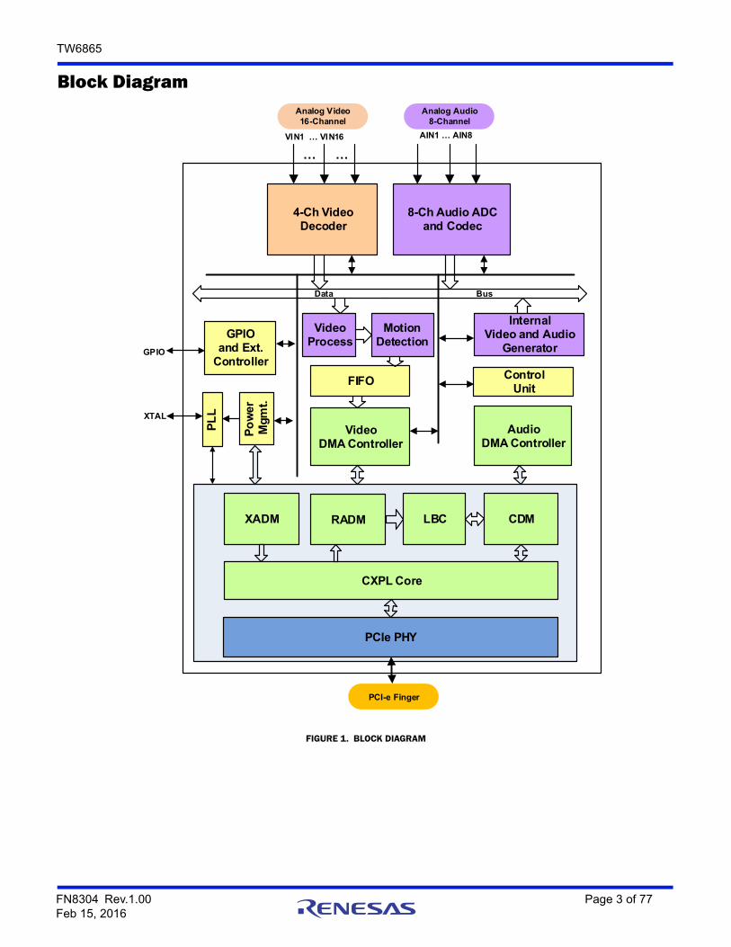
Block Diagram
FIGURE 1. BLOCK DIAGRAM
8-Ch Audio ADCand Codec
4-Ch Video Decoder
Video DMA Controller
ControlUnit
Internal Video and Audio
Generator
Analog Video16-Channel
Analog Audio8-Channel
GPIO and Ext.
Controller
PLL
Bus Data
Pow
er M
gmt.
GPIO
XTAL
VIN1 … VIN16 AIN1 … AIN8
… …
Video Process
XADM RADM LBC CDM
CXPL Core
PCIe PHY
AudioDMA Controller
PCI-e Finger
FIFO
MotionDetection
FN8304 Rev.1.00 Page 3 of 77Feb 15, 2016
TW6865
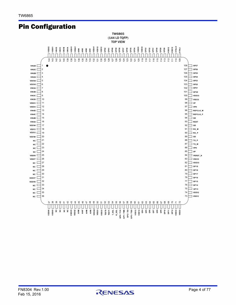
Pin ConfigurationTW6865
(144 LD TQFP)TOP VIEW
GP
42
GP
41
GP
40
GP
39
PERST _N
TW6865
37 38 39 40 41 42 43 44 45 46 47 48 49 50 51 52 53 54 55 56 57 58 59 60 61 62 63 64 65 66 67 68
144
143
142
141
140
139
138
137
136
135
134
133
132
131
130
129
128
127
126
125
124
123
122
121
120
119
118
117
116
115
114
113
1
2
3
4
5
6
7
8
9
10
11
12
13
14
15
16
17
18
19
20
21
22
23
24
25
26
27
28
29
30
31
32
104
103
102
101
100
99
98
97
96
95
94
93
92
91
90
89
88
87
86
85
84
83
82
81
80
79
78
77
76
75
74
73
GP
38
GP
37
GP
36
GP
35
GP
34
VS
S3
3
VD
D33
VSS12
VPH
TX_M
TX_P
RX_P
GD
RX_M
GD
REXT
REFCLK_M
REFCLK_P
VDD12
GP16
GP17
GP26
GP18
VD
DA
1
VD
D12
XTA
LO
VSS33
GP13
VPH
VP
GP15
GD
VP
33
34
35
36
69 70 71 72
GP
33
GP
32
GP
31
GP
30
108
107
106
105
112
111
110
109
XTA
LI
VS
S1
2
VD
D12
VS
S1
2
GP19
GP20
VDD33
GP21
VSS33
GP22
GP23
AIN
1
GP24
GP25
GP27
AIN
2
AIN
3
VS
SA
1
VD
DV
5
NC
NC
NC
AIN
4
VS
SV
5
NC
GP
29
GP
28
VDD33
GP14
VIN2D
VIN2B
VIN2C
VDDV2
VIN2A
VIN3A
VDDV3
VIN3C
VIN3B
VSSV3
VIN3D
VIN4D
VIN4B
VIN4C
VDDV4
VIN4A
VSSV4
VSS12
VDD12
VS
SV
6
VD
DV
1
VIN
1A
VIN
1B
VIN
1C
VS
SV
1
VIN
1D
TQFP-144L 20x20
NC
NC
NC
VSSV8
NC
NC
VSSV7
NC
NC
VDDV7
NC
NC
NC
NC
VDDV8
NC
VDDV6
VS
SV
2
VD
DA
2
AIN
5
AIN
6
AIN
7
VS
SA
2
AIN
8
TES
T1
TES
T0
VD
D3
3
VS
S3
3
VD
D1
2
VS
S1
2
R_
SE
L
T_S
EL
VS
S3
3
GP
1 /
TM
S
GP
2 /
TD
I
GP
0 /
TC
K
GP
3 /
TD
O
GP
4
GP
12
VD
D3
3
GP
5
GP
6
GP
7
GP
8
GP
9
GP
10
GP
11
FN8304 Rev.1.00 Page 4 of 77Feb 15, 2016

TW6865
Pin DescriptionsNAME NUMBER TYPE DESCRIPTION
ANALOG INTERFACE PINS (24)
VIN1A 139 A Composite video inputs
VIN1B 140 A Composite video inputs
VIN1C 141 A Composite video inputs
VIN1D 142 A Composite video inputs
VIN2A 4 A Composite video inputs
VIN2B 3 A Composite video inputs
VIN2C 2 A Composite video inputs
VIN2D 1 A Composite video inputs
VIN3A 7 A Composite video inputs
VIN3B 8 A Composite video inputs
VIN3C 9 A Composite video inputs
VIN3D 10 A Composite video inputs
VIN4A 16 A Composite video inputs
VIN4B 15 A Composite video inputs
VIN4C 14 A Composite video inputs
VIN4D 13 A Composite video inputs
AIN1 133 A Analog audio inputs
AIN2 134 A Analog audio inputs
AIN3 135 A Analog audio inputs
AIN4 136 A Analog audio inputs
AIN5 48 A Analog audio inputs
AIN6 47 A Analog audio inputs
AIN7 46 A Analog audio inputs
AIN8 45 A Analog audio inputs
PCI EXPRESS INTERFACE (7)
TX_M 87 O High-Speed Differential Transmit Pair
TX_P 88 O
RX_P 90 I High-Speed Differential Receive Pair
RX_M 91 I
REXT 93 IO Reference Resistor Connection. 190Ω 1% precision resistor to ground
REFCLK_P 95 I Differential Reference Clock Input
REFCLK_M 96 I
FN8304 Rev.1.00 Page 5 of 77Feb 15, 2016

TW6865
SYSTEM CONTROL PINS (50)
XTALI 109 IO System reference clock crystal input (27MHz)
XTALO 110 IO System reference clock crystal output
PERST_N 84 I System reset.
TEST[1:0] 53, 52 I Test mode selection, tie to ground
GP[42:0] 129, 128, 127, 126, 125, 124, 123, 122, 121, 118, 117, 116, 115, 114, 113, 108, 107, 106, 105, 104,
103, 102, 101, 81, 80, 79, 78, 77, 76, 75, 70, 69, 68, 67, 66, 65, 64, 63, 62, 59,
58, 57, 56
IO GPIO control ports
T_SEL 54 I NC
R_SEL 55 I NC
POWER/GROUND PINS (47)
VP 85, 98 P Low-Voltage Supply (1.2V)
VPH 86, 97 P High-Voltage I/O Supply (3.3V)
GD 89, 92, 94 G Digital Ground
VDD33 51, 71, 82, 100, 119 P Digital I/O Power, 3.3V
VSS33 50, 72, 83, 99, 120 G Digital Ground
VDD12 19, 61, 74, 111, 131 P Digital Core Power, 1.2V
VSS12 18, 60, 73, 112, 130 G Digital Core Ground
VDDAx 132, 49 P Analog Power for Audio ADC, 3.3V
VSSAx 137, 44 G Analog Ground for Audio ADC
VDDVx 138, 5, 6, 17, 20, 31, 32, 43
P Analog Power for Video ADC, 3.3V
VSSVx 143, 144, 11, 12, 25, 26, 37, 38
G Analog Ground for Video ADC
NC PINS (16)
NC 21, 22, 23, 24, 27, 28, 29, 30, 33, 34, 35, 36, 39, 40,
41, 42
No Connection
Pin Descriptions (Continued)
NAME NUMBER TYPE DESCRIPTION
Ordering InformationPART NUMBER
(Notes 1, 2) PART MARKINGTEMP RANGE
(°C)PACKAGE
(RoHS Compliant)PKG.
DWG. #
TW6865-TA1-CR TW6865 TA1-CR 0 to +70 144 Ld TQFP (20mmx20mm Q144.20x20C
TW6865-TA1-CRH (Note 3) TW6865 TA1-CRH -40 to +85 144 Ld TQFP (20mmx20mm Q144.20x20C
NOTES:
1. These Intersil Pb-free plastic packaged products employ special Pb-free material sets, molding compounds/die attach materials, and 100% matte tin plate plus anneal (e3 termination finish, which is RoHS compliant and compatible with both SnPb and Pb-free soldering operations). Intersil Pb-free products are MSL classified at Pb-free peak reflow temperatures that meet or exceed the Pb-free requirements of IPC/JEDEC J STD-020.
2. For Moisture Sensitivity Level (MSL), please see product information page for TW6865. For more information on MSL, please see tech brief TB363.
3. “H” version supports Industrial Temperature operation. See “SUPPLY CURRENT AND POWER DISSIPATION” on page 8.
FN8304 Rev.1.00 Page 6 of 77Feb 15, 2016

TW6865
Absolute Maximum Ratings Thermal InformationSupply Pins
VDDAVM, VDDA (Measured to VSSA) . . . . . . . . . . . . . . . . . . . .-0.5 to 4.5VVDDVAM, VDDV (Measured to VSSV). . . . . . . . . . . . . . . . . . . . .-0.5 to 4.5VVDD12M, VDD12 (Measured to VSS12). . . . . . . . . . . . . . . . . .-0.5 to 2.3VVDD33M, VDD33 (Measured to VSS33). . . . . . . . . . . . . . . . . .-0.5 to 4.5V
ESD RatingsHuman Body Model (JS-001-2010) . . . . . . . . . . . . . . . . . . . . . . . . . . . 2kVCharged Device Model (JESD22-C101E) . . . . . . . . . . . . . . . . . . . . . . 750V
Thermal Resistance (Typical) JA (°C/W) JC (°C/W)144 Ld TQFP Package (Notes 4, 5) . . . . . . 41 7
Power Dissipation. . . . . . . . . . . . . . . . .See Electrical Specifications page 8Maximum Die Temperature . . . . . . . . . . . . . . . . . . . . . . . . . . . . . . . .+125°CStorage Temperature . . . . . . . . . . . . . . . . . . . . . . . . . . . . . .-65°C to +150°CPb-Free Reflow Profile . . . . . . . . . . . . . . . . . . . . . . . . . . . . . . . . . . see TB493
Recommended Operating ConditionsAmbient Operating Temperature
CR . . . . . . . . . . . . . . . . . . . . . . . . . . . . . . . . . . . . . . . . . . . . . . 0°C to +70°CCRH . . . . . . . . . . . . . . . . . . . . . . . . . . . . . . . . . . . . . . . . . . . -40°C to +85°C
VDDA (Measured to VSSA), VDDAVM . . . . . . . . . . . . . . . . . . . . . 3.0V to 3.6VVDDV (Measured to VSSV), VDDVAM. . . . . . . . . . . . . . . . . . . . . . 3.0V to 3.6VVDD12 (Measured to VSS12), VDD12M. . . . . . . . . . . . . . . . .1.08V to 1.32VVDD33 (Measured to VSS33), VDD33M. . . . . . . . . . . . . . . . . . . . 3.0 to 3.6V
CAUTION: Do not operate at or near the maximum ratings listed for extended periods of time. Exposure to such conditions may adversely impact productreliability and result in failures not covered by warranty.
NOTES:
4. JA is measured with the component mounted on a high effective thermal conductivity test board in free air. See Tech Brief TB379 for details.
5. For JC, the “case temp” location is taken at the package top center.
Electrical Specifications Boldface limits apply across the operating temperature range, -0°C to +70°C or -40°C to 85°C.
PARAMETER SYMBOLMIN
(Note 8) TYPMAX
(Note 8) UNIT
DIGITAL INPUTS
Input High Voltage (TTL) VIH 2.0 3.6 V
Input Low Voltage (TTL) VIL -0.3 0.8 V
Input Leakage Current (At VI = 2.5V or 0V) IL ±10 µA
Input Capacitance CIN 6 pF
DIGITAL OUTPUTS
Output High Voltage VOH 2.4 V
Output Low Voltage VOL 0.4 V
High Level Output Current (At VOH = 2.4V) IOH 9.3 18.2 29.2 mA
Low Level Output Current (At VOL = 0.4V)
IOL 7.4 11.8 16.5 mA
Tri-State Output Leakage Current (At VO = 2.5V or 0V) IOZ ±10 µA
Output Capacitance CO 6 pF
Analog Pin Input Capacitance CA 6 pF
FN8304 Rev.1.00 Page 7 of 77Feb 15, 2016

TW6865
SUPPLY CURRENT AND POWER DISSIPATION
Analog Video Supply Current (VDDV, 3.3V) IDDV 110 mA
Analog Audio Supply Current (VDDA, 3.3V) IDDA 37 mA
Digital Internal Supply Current (VDD12, 1.2V) IDDI 190 mA
Digital I/O Supply Current (VDDV, 3.3V) IDDS 4 mA
PCIe Core Current (VP, 1.2V) IVP 21 mA
PCIe IO Current (VPH, 3.3V) IVPH 21 mA
Ambient Operating Temperature 0 +70 °C
Ambient Operating Temperature (H version only) -40 +85 °C
Total Power Dissipation P 820.7 mW
VIDEO DECODER PARAMETER 1
ADCs
ADC Resolution ADCR 10 Bits
ADC Integral Nonlinearity AINL ±1 LSB
ADC Differential Nonlinearity ADNL ±1 LSB
ADC Clock Rate fADC 24 27 30 MHz
Video Bandwidth (-3dB) BW 10 MHz
Horizontal PLL
Line Frequency (50Hz) fLN 15.625 kHz
Line Frequency (60Hz) fLN 15.734 kHz
Static Deviation fH 6.2 %
Subcarrier PLL
Subcarrier Frequency (NTSC-M) fSC 3.579545 MHz
Subcarrier Frequency (PAL-BDGHI) fSC 4.433619 MHz
Subcarrier Frequency (PAL-M) fSC 3.575612 MHz
Subcarrier Frequency (PAL-N) fSC 3.582056 MHz
Lock-In Range fH Hz
Oscillator Input
Nominal Frequency 27 MHz
Deviation ±50 ppm
Duty cycle 55 %
Electrical Specifications Boldface limits apply across the operating temperature range, -0°C to +70°C or -40°C to 85°C. (Continued)
PARAMETER SYMBOLMIN
(Note 8) TYPMAX
(Note 8) UNIT
FN8304 Rev.1.00 Page 8 of 77Feb 15, 2016

TW6865
VIDEO DECODER PARAMETER 2
Lock Specification
Sync Amplitude Range 1 200 %
Color Burst Range 5 200 %
Horizontal Lock Range -5 5 %
Vertical Lock Range 45 65 Hz
fsc Lock Range ±450 Hz
Color Burst Position Range ±2.2 µs
Color Burst Width Range 1 cycle
Video Bandwidth
B/W 6 MHz
Noise Specification
SNR (Luma Flat Field) 57 dB
Non-linear Specification
Y Non-Linearity 0.5 0.7 %
Differential Phase DP 0.4 0.6 °
Differential Gain DG 0.6 0.8 %
Chroma Specification
Hue Accuracy 1 °
Chroma ACC Range 400 %
Chroma Amplitude Error 1 %
Chroma Phase Error 0.3 %
Chroma Luma Intermodulation 0.2 %
K-Factor
K2T 0.5 %
Kpulse/Bar 0.5 %
ANALOG AUDIO INPUT CHARACTERISTICS
AIN1-4 Input Impedance RINX 10 kΩ
Interchannel Gain Mismatch 0.2 dB
Input Voltage Range 2 VP-P
Full Scale Input Voltage (Note 6) ViFULL 1 VP-P
Interchannel Isolation (Note 7) 90 dB
NOTES:
6. Tested at input gain of 0 dB, FIN = 1kHz.
7. Tested at input gain of 0 dB, FS = 8kHz and 16kHz.
8. Parameters with MIN and/or MAX limits are tested at +25°C, unless otherwise specified. Temperature limits established by characterization and are not production tested.
Electrical Specifications Boldface limits apply across the operating temperature range, -0°C to +70°C or -40°C to 85°C. (Continued)
PARAMETER SYMBOLMIN
(Note 8) TYPMAX
(Note 8) UNIT
FN8304 Rev.1.00 Page 9 of 77Feb 15, 2016

TW6865
Functional DescriptionVideo Decoder
VIDEO INPUT FORMATSThe TW6865 has built-in automatic standard discrimination circuitry. The circuit uses burst-phase, burst-frequency and frame rate to identify NTSC, PAL or SECAM color signals. The standards that can be identified are NTSC (M), NTSC (4.43), PAL (B, D, G, H, I), PAL (M), PAL (N), PAL (60) and SECAM (M). Each standard can be included or excluded in the standard recognition process by software control. The exceptions are the base standard NTSC and PAL, which are always enabled. The identified standard is indicated by the Standard Selection (SDT) register. Automatic standard detection can be overridden by software controlled standard selection.
TW6865 supports all common video formats as shown in Table 2.
ANALOG FRONTENDThe TW6865 contains four 10-bit ADC (Analog to Digital Converters) to digitize the analog video inputs. The ADC can be put into power-down mode by the V_ADC_PWDN register. The TW6865 also contains an anti-aliasing filter to prevent out-of-band frequency in analog video input signal. Therefore, there is no need for external components in the analog input pin except for an AC coupling capacitor and a termination resistor. Figure 2 shows the frequency response of the anti-aliasing filter.
TABLE 2. VIDEO INPUT FORMATS SUPPORTED BYTW6865
FORMAT LINES FIELDSfSC
(MHz) COUNTRY
NTSC-M 525 60 3.579545 U.S., many others
NTSC-Japan (Note 9)
525 60 3.579545 Japan
PAL-B, G, N 625 50 4.433619 Many
PAL-D 625 50 4.433619 China
PAL-H 625 50 4.433619 Belgium
PAL-I 625 50 4.433619 Great Britain, others
PAL-M 525 60 3.575612 Brazil
PAL-CN 625 50 3.582056 Argentina
SECAM 625 50 4.406, 4.250 France, Eastern Europe, Middle East, Russia
PAL-60 525 60 4.433619 China
NTSC (4.43) 525 60 4.433619 Transcoding
NOTE:9. NTSC-Japan has 0 IRE setup.
0 0.2 0.4 0.6 0.8 1 1.2 1.4 1.6 1.8 2
x 107
-40
-35
-30
-25
-20
-15
-10
-5
0
Frequency (Hertz)
Gai
n (d
B)
FIGURE 2. THE FREQUENCY RESPONSE OF ANTI-ALIASING FILTER
0
-5
-10
-15
-20
-25
-30
-35
-400 0.2 0.4 0.6 0.8 1.0 1.2 1.4 1.6 1.8 2.0
FREQUENCY (Hz) x107
GA
IN (
dB
)
FN8304 Rev.1.00 Page 10 of 77Feb 15, 2016
TW6865
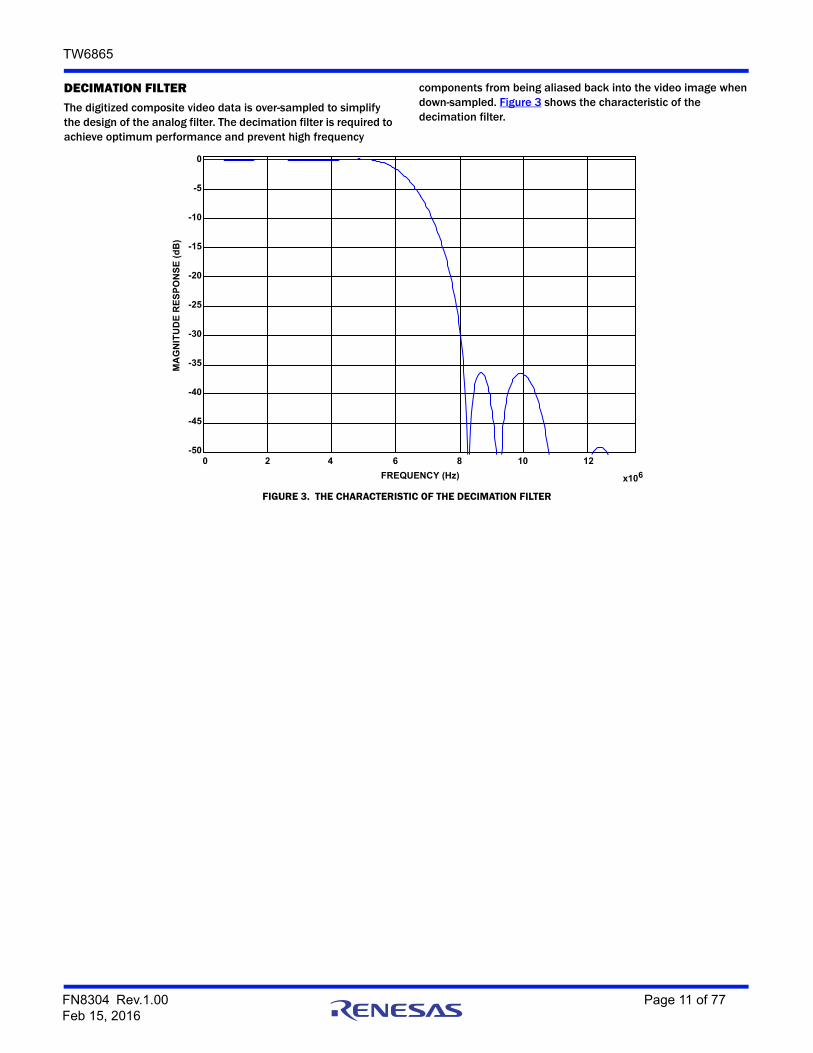
DECIMATION FILTERThe digitized composite video data is over-sampled to simplify the design of the analog filter. The decimation filter is required to achieve optimum performance and prevent high frequency
components from being aliased back into the video image when down-sampled. Figure 3 shows the characteristic of the decimation filter.
0 2 4 6 8 10 12
x 106
-50
-45
-40
-35
-30
-25
-20
-15
-10
-5
0
Frequency (Hertz)
Mag
nitu
de R
espo
nse
(dB
)
FIGURE 3. THE CHARACTERISTIC OF THE DECIMATION FILTER
0
-5
-10
-15
-20
-25
-30
-35
-40
FREQUENCY (Hz) x106
MA
GN
ITU
DE
RE
SP
ON
SE
(d
B)
-45
-500 2 4 6 8 10 12
FN8304 Rev.1.00 Page 11 of 77Feb 15, 2016

TW6865
AUTOMATIC GAIN CONTROL AND CLAMPINGAll four analog channels have built-in clamping circuits that restore the signal DC level. The Y channel restores the back porch of the digitized video to a level of 60. This operation is automatic through internal feedback loop. The Automatic Gain Control (AGC) of the Y channel adjusts input gain so that the sync tip is at a desired level. Programmable white peak protection logic is included to prevent saturation in the case of abnormal signal proportion between sync and white peak level.
SYNC PROCESSINGThe sync processor of TW6865 detects horizontal synchronization and vertical synchronization signals in the composite video or in the Y signal of an S-video or component signal. The processor contains a digital phase-locked-loop and decision logic to achieve reliable sync detection in stable signal as well as in unstable signals, such as those from VCR fast forward or backward.
The vertical sync separator detects the vertical synchronization pattern in the input video signals. In addition, the actual sync determination is controlled by a detection window to provide more reliable synchronization. An option is available to provide faster responses for certain applications. The field status is determined at vertical synchronization time. The field logic can also be controlled to toggle automatically while tracking the input.
Y/C SEPARATIONThe color decoding block contains the luma/chroma separation for the composite video signal and multistandard color demodulation. For NTSC and PAL standard signals, the luma/chroma separation can be done either by comb filter or notch/band-pass filter combination. For SECAM standard signals, adaptive notch/band-pass filter is used. The default selection for NTSC/PAL is comb filter.
In the case of comb filter, the TW6865 separates luma (Y) and chroma (C) of a NTSC/PAL composite video signal using a proprietary 4H adaptive comb filter. The filter uses a four-line buffer. Adaptive logic combines the upper comb and the lower comb results based on the signal changes among the previous, current and next lines. This technique leads to excellent Y/C separation with small cross luma and cross color at both horizontal and vertical edges
Due to the line buffer used in the comb filter, there are always two lines processing delay at the output except for the component input mode, which has only one line delay.
If notch/band-pass filter is selected, the characteristics of the filters are shown in the filter curve section.
Figures 4 shows the frequency response of the notch filter for each system NTSC and PAL. Figure 5 on page 13 shows the frequency response of Chroma Band Pass Filter Curves.
0 1 2 3 4 5 6 7 8
x 106
-45
-40
-35
-30
-25
-20
-15
-10
-5
0
5
Frequency (Hertz)
Gai
n (d
B)
FIGURE 4. THE CHARACTERISTICS OF LUMINANCE NOTCH FILTER
0 1 2 3 4 5 6 7 8
FREQUENCY (Hz) x106
GA
IN (
dB
)
5
0
-5
-10
-15
-20
-25
-30
-35
-40
-45
NTSC PAL
FN8304 Rev.1.00 Page 12 of 77Feb 15, 2016

TW6865
0 1 2 3 4 5 6 7 8 9
x 106
-50
-45
-40
-35
-30
-25
-20
-15
-10
-5
0
Frequency (Hertz)
Mag
nitu
de R
espo
nse
(dB
)
FIGURE 5. FREQUENCY RESPONSE OF CHROMA BAND PASS FILTER CURVES
0
-5
-10
-15
-20
-25
-30
-35
-40
FREQUENCY (Hz) x106
MA
GN
ITU
DE
RE
SP
ON
SE
(d
B)
-45
-500 2 3 4 5 7 81 6 9
NTSC PAL/SEAM
FN8304 Rev.1.00 Page 13 of 77Feb 15, 2016
TW6865
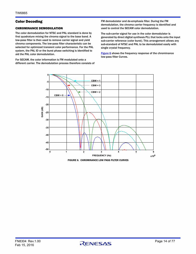
Color Decoding
CHROMINANCE DEMODULATIONThe color demodulation for NTSC and PAL standard is done by first quadrature mixing the chroma signal to the base band. A low-pass filter is then used to remove carrier signal and yield chroma components. The low-pass filter characteristic can be selected for optimized transient color performance. For the PAL system, the PAL ID or the burst phase switching is identified to aid the PAL color demodulation.
For SECAM, the color information is FM modulated onto a different carrier. The demodulation process therefore consists of
FM demodulator and de-emphasis filter. During the FM demodulation, the chroma carrier frequency is identified and used to control the SECAM color demodulation.
The sub-carrier signal for use in the color demodulator is generated by direct digital synthesis PLL that locks onto the input sub-carrier reference (color burst). This arrangement allows any sub-standard of NTSC and PAL to be demodulated easily with single crystal frequency.
Figure 6 shows the frequency response of the chrominance low-pass filter Curves.
0 1 2 3 4 5 6
x 106
-50
-45
-40
-35
-30
-25
-20
-15
-10
-5
0
Frequency (Hertz)
Gai
n (d
B)
FIGURE 6. CHROMINANCE LOW PASS FILTER CURVES
0 1 2 3 4 5 6
FREQUENCY (Hz) x106
GA
IN (
dB
)
0
-5
-10
-15
-20
-25
-30
-35
-40
-45
-50
CBW = 0
CBW = 3
CBW = 1
CBW = 2
FN8304 Rev.1.00 Page 14 of 77Feb 15, 2016

TW6865
ACC (AUTOMATIC COLOR GAIN CONTROL)The Automatic Chroma Gain Control (ACC) compensates for reduced amplitudes caused by high-frequency loss in video signal. In the NTSC/PAL standard, the color reference signal is the burst on the back porch. It is measured to control the chroma output gain. The range of ACC control is –6dB to +24dB.
Chrominance Processing
CHROMINANCE GAIN, OFFSET AND HUE ADJUSTMENTWhen decoding NTSC signals, TW6865 can adjust the hue of the chroma signal. The hue is defined as a phase shift of the subcarrier with respect to the burst. This phase shift of NTSC decoding can be programmed through a control register. For the PAL standard, the PAL delay line is provided to compensate any hue error; therefore, there is no hue adjustment available. The color saturation can be adjusted by changing the gain of Cb and Cr signals for all NTSC, PAL and SECAM formats. The Cb and Cr gain can be adjusted independently for flexibility.
CTI (COLOR TRANSIENT IMPROVEMENT)The TW6865 provides the Color Transient Improvement function to further enhance the image quality. The CTI enhance the color edge transient without any overshoot or undershoot.
LUMINANCE PROCESSINGThe TW6865 adjusts brightness by adding a programmable value (in register BRIGHTNESS) to the Y signal. It adjusts the picture contrast by changing the gain (in register CONTRAST) of the Y signal.
The TW6865 also provide programmable peaking function to further enhance the video sharpness. The peaking control has built-in coring function to prevent enhancement of noise.
Figure 7 shows the characteristics of the peaking filter for four different gain modes and different center frequencies.
0 1 2 3 4 5 6 7
x 106
0
2
4
6
8
10
12
14
16
Frequency (Hertz)
Mag
nitu
de R
espo
nse
(dB
)
FIGURE 7. CHARACTERISTICS OF THE PEAKING FILTER
16
14
12
10
8
6
4
2
FREQUENCY (Hz) x106
MA
GN
ITU
DE
RE
SP
ON
SE
(d
B)
0 2 3 4 5 71 6
0
FN8304 Rev.1.00 Page 15 of 77Feb 15, 2016

TW6865
Video CroppingCropping allows only subsection of a video image to be output. The active video region is determined by HDELAY, HACTIVE, VDELAY and VACTIVE register as illustrated in Figure 8. The VACTIVE signal can be programmed to indicate the number of active lines to be displayed in a video field, and the HACTIVE signal can be programmed to indicate the number of active pixels to be displayed in a video line. The start of the field or frame in the vertical direction is indicated by the leading edge of VSYNC. The start of the line in the horizontal direction is indicated by the leading edge of the HSYNC. The start of the active lines from vertical sync edge is indicated by the VDELAY register. The start of the active pixels from the horizontal edge is indicated by the HDELAY register. The sizes and location of the active video are determined by HDELAY, HACTIVE, VDELAY and VACTIVE registers. These registers are 8-bit wide, the lower 8 bits is, respectively, in HDELAY_LO, HACTIVE_LO, VDELAY_LO and VACTIVE_LO. Their upper 2-bit shares the same register CROP_HI.
The Horizontal Delay register (HDELAY) determines the number of pixels delay between the leading edge of HSYNC and the leading edge of the HACTIVE. Note that this value is referenced to the unscaled pixel number. The Horizontal active register (HACTIVE) determines the number of active pixels to be output or scaled after the delay from the sync edge is met. This value is also referenced to the unscaled pixel number. Therefore, if the scaling ratio is changed, the active video region used for scaling remain unchanged as set by the HACTIVE register, but the valid pixels output are equal or reduced due to down scaling. In order for the cropping to work properly, the following equation should be satisfied.
HDELAY + HACTIVE < Total number of pixels per line
For NTSC output at 13.5MHz pixel rate, the total number of pixels is 858. For PAL output at 13.5MHz rate, the total number of pixels is 864. HACTIVE should be set to 720.
The Vertical Delay register (VDELAY) determines the number of lines delay between the leading edge of the VSYNC and the start of the active video lines. It indicates number of lines to skip at the start of a frame before asserting the VACTIVE signal. This value is referenced to the incoming scan lines before the vertical scaling. The number of scan lines is 525 for the 60Hz systems and 625 for the 50Hz systems. The Vertical Active register
(VACTIVE) determines the number of lines to be used in the vertical scaling. Therefore, the number of scan lines output is equal or less than the value set in this register depending on the vertical scaling ratio. In order for the vertical cropping to work properly, the following equation should be observed.
VDELAY + VACTIVE < Total number of lines per field
Video ScalerThe TW6865 can independently reduce the output video image size in both horizontal and vertical directions using arbitrary scaling ratios up to 1/16 in each direction. The horizontal scaling employs a dynamic 6-tap 32-phase interpolation filter for luma and a 2-tap 8-phase interpolation filter for chroma because of the limited bandwidth of the chroma data. The vertical scaling uses simple line dropping algorithm. Therefore, the use of non-integer vertical scaling ration is not recommended.
Downscaling is achieved by programming the Horizontal Scaling ratio register (HSCALE) and Vertical Scaling ratio register (VSCALE). When outputting unscaled video, the TW6865 will output CCIR601 compatible 720 pixels per line or any number of pixels per line as specified by the HACTIVE register. The standard output for square pixel mode is 640 pixels for 60Hz system and 768 pixels for 50Hz systems. If the number of output pixels required is smaller than 720 in CCIR601 compatible mode or the number specified by the HACTIVE register, the 12-bit HSCALE register, which is the concatenation of two 8-bit registers SCALE_HI and HSCALE_LO, is used to reduce the output pixels to the desired number.
Following is an example using pixel ratio to determine the horizontal scaling ratio. Equations 1 and 2 should be used to determine the scaling ratio to be written into the 12-bit HSCALE register assuming HACTIVE is programmed with 720 active pixels per line:
Where: Npixel_desired is the nominal number of pixel per line.
For example, to output a CCIR601 compatible NTSC stream at SIF resolution, the HSCALE value can be found as shown by Equation 3:
However, to output a SQ compatible NTSC stream at SIF resolution, the HSCALE value should be found as shown by Equation 4:
In this case, with total resolution of 768 per line, the HACTIVE should have a value of 640.
VD
EL
AY
VA
CT
IVE
HDELAY HACTIVE
V reference
H reference
FIGURE 8. THE EFFECT OF CROPPING REGISTERS
NTSC: HSCALE 720 Npixel_desired 256= (EQ. 1)
PAL: HSCALE 720 Npixel_desired 256= (EQ. 2)
HSCALE 720 320 256 576 0x0240= = = (EQ. 3)
HSCALE 640 320 256 512 0x200= = = (EQ. 4)
FN8304 Rev.1.00 Page 16 of 77Feb 15, 2016

TW6865
The vertical scaling determines the number of vertical lines output by the TW6865. The Vertical Scaling register (VSCALE) is a 12-bit register, which is the concatenation of a 4-bit register SCALE_HI and an 8-bit register VSCALE_LO. The maximum scaling ratio is 16:1. Equations 5 and 6 should be used to determine the scaling ratio to be written into the 12-bit VSCALE register assuming VACTIVE is programmed with 240 or 288 active lines per field.
Where: Nline_desired is the number of active lines output per field.
The scaling ratios for some popular formats are listed in Table 3. Figure 9 shows the Horizontal Scaler Prefilter Curve.
60Hz system: VSCALE 240 Nline_desired 256= (EQ. 5)
50Hz system: VSCALE 288 Nline_desired 256= (EQ. 6)
TABLE 3. HSCALE and VSCALE VALUES FOR SOME POPULAR VIDEO FORMATS
SCALING RATIO FORMAT TOTAL RESOLUTION OUTPUT RESOLUTION HSCALE VALUES VSCALE (FRAME)
1:1 NTSC SQNTSC CCIR601PAL SQPAL CCIR601
780x525858x525944x625864x625
640x480720x480768x576720x576
0x01000x01000x01000x0100
0x01000x01000x01000x0100
2:1 (CIF) NTSC SQNTSC CCIR601PAL SQPAL CCIR601
390x262429x262472x312432x312
320x240360x240384x288360x288
0x02000x02000x02000x0200
0x02000x02000x02000x0200
4:1 (QCIF) NTSC SQNTSC CCIR601PAL SQPAL CCIR601
195x131214x131236x156216x156
160x120180x120192x144180x144
0x04000x04000x04000x0400
0x04000x04000x04000x0400
HFLT[1:0]=3
HFLT[1:0]=2HELT[1:0] = 3
0 0.05 0.1 0.15 0.2 0.25 0.3 0.35 0.4 0.45 0.5-40
-35
-30
-25
-20
-15
-10
-5
0
Fsig/Fsample
Mag
nitu
de R
espo
nse
(dB
)
FIGURE 9. HORIZONTAL SCALER PREFILTER CURVE
0
-5
-10
-15
-20
-25
-30
-35
FSIG/FSAMPLE
MA
GN
ITU
DE
RE
SP
ON
SE
(d
B)
-40
HELT[1:0] = 1
0 0.05 0.10 0.15 0.20 0.25 0.30 0.35 0.40 0.45 0.50
HELT[1:0] = 2
HELT[1:0] = 3
FN8304 Rev.1.00 Page 17 of 77Feb 15, 2016
TW6865
Motion DetectionThe TW6865 supports a motion detector for each of the 8 video decoders. The built-in motion detection algorithm uses the difference of luminance level between current and the reference field. To detect motion properly according to situation needed, the TW6865 provides several sensitivity and velocity control parameters for each motion detector. The TW6865 supports manual strobe function to update motion detection so that it is more appropriate for user-defined motion sensitivity control. When motion is detected in any video inputs, the TW6865 updates its motion status registers. Through which the host processor can read the motion information.
Audio CodecThe audio codec in the TW6865 is composed of 8 audio analog-to-digital converters, audio mixer and audio detector. The TW6865 can accept 8 analog audio signals, and produce 8-channel digital audio data.
The level of analog audio input signal AIN1 ~ AIN8 can be adjusted respectively by internal programmable gain amplifiers that are defined via the AIGAIN1, AIGAIN2, AIGAIN3 and AIGAIN4 registers and then sampled by each analog-to-digital converter.
The TW6865 can mix all of analog audio inputs according to the predefined mixing ratio for each audio via the MIX_RATIO1 ~ MIX_RATIO4 registers. This mixing audio output can also be transferred through PCIe interface.
Audio DetectionThe TW6865 has an audio detector for individual 8 channels. There are 2 kinds of audio detection method defined by the AAMPMD. One is the detection of absolute amplitude and the other is of differential amplitude. For both detection methods, the accumulating period is defined by the ADET_FILT register and the detecting threshold value is defined by the ADET_TH1 ~ ADET_TH4 registers.
DMA ControllerThis module mainly packs the received video and audio data to the defined maximum payload size and manages the target address of each transaction layer package. It uses round-robin arbitration among DMA channels to choose current on-duty one. The Legacy PCI INT_A compatible interrupt emulation is supported to interrupt PC.
Internal Video And Audio GeneratorTo assist video debugging, this generator outputs 8 different colorbar patterns for each video DMA channel. Each colorbar pattern includes 7 vertical color bars and 1 horizontal black/grey color whose position and width are adjustable.
To assist audio debugging, this generator outputs 8 different single tones with adjustable sampling rate. The 9th audio pattern is a mixing mode whose tone is chosen from one of others with register setting.
Control UnitThis module handles configuration and control through PCIe to all internal blocks and registers such as DMA controller and PCIe endpoint controller.
GPIO And External ControllerThis module controls all GPIO pins, configures external TW2864 through serial control pins (SCLK and SDAT) and resets external TW2864 through RST_TO_2864 pin.
PCI Express End Point ControllerThis controller contains three main PCI Express protocol layers: Transaction later, Data Link Layer, and Physical Layer. It complies with PCI Express Base Specification, Revision 1.1, and PCI Express 2.0 Base Specification, Revision 2.0. It works with external x1 PHY through the standard PHY Interface for PCI Express (PIPE).
PCI Express PHYThis module is the PCI express physical layer.
FN8304 Rev.1.00 Page 18 of 77Feb 15, 2016
TW6865
Host InterfaceThe TW6865 provides with PCI Express interface for programming and controlling.
Register Description
DMA CONTROLLER
INDEX
INT_STATUS
DEFAULT[7] [6] [5] [4] [3] [2] [1] [0]
0x00 B3 RSV RSV RSV RSV BAD_FMT_3
BAD_FMT_2
BAD_FMT_1
BAD_FMT_0
0x00
B2 0 0 0 0 0 0 DMA_TOUT 0 0x00
B1 INTSTA_DMA15
INTSTA_DMA14
INTSTA_DMA13
INTSTA_DMA12
INTSTA_DMA11
INTSTA_DMA10
INTSTA_DMA9
INTSTA_DMA8
0x00
B0 RSV RSV RSV RSV INTSTA_DMA3
INTSTA_DMA2
INTSTA_DMA1
INTSTA_DMA0
0x00
BAD_FMT_3 B[27] Bad incoming data format flag of video input -30 = No error detected 1 = Wrong format detected from the incoming data * This bit status is controlled by DMA_CONFIG[27:24]** BAD_FMT = P_BAD | P_OVSee register VIDEO_PARSER_STATUS
BAD_FMT_2 B[26] Bad incoming data format flag of video input -2BAD_FMT_1 B[25] Bad incoming data format flag of video input -1BAD_FMT_0 B[24] Bad incoming data format flag of video input -0
DMA_TOUT B[17] Time out flag of DMA channels
INTSTA_DMA[15:8] B[15:8] Interrupt request from DMA Channel-15 to Channel-80 = No interrupt1 = Interrupt
INTSTA_DMA[3:0] B[3:0] Interrupt request from DMA Channel-3 to Channel-00 = No interrupt1 = Interrupt
FN8304 Rev.1.00 Page 19 of 77Feb 15, 2016

TW6865
INDEX
PB_STATUS
DEFAULT[7] [6] [5] [4] [3] [2] [1] [0]
0x01 B3 RSV RSV RSV RSV FFLAG_DMA3
FFLAG_DMA2
FFLAG_DMA1
FFLAG_DMA0
0x00
B2 0 0 0 0 0 0 0 0 0x00
B1 PBFLAG_DMA15
PBFLAG_DMA14
PBFLAG_DMA13
PBFLAG_DMA12
PBFLAG_DMA11
PBFLAG_DMA10
PBFLAG_DMA9
PBFLAG_DMA8
0xFF
B0 RSV RSV RSV RSV PBFLAG_DMA3
PBFLAG_DMA2
PBFLAG_DMA1
PBFLAG_DMA0
0xFF
FFLAG_DMA3 B[27] Field flag of DMA Channel-30 = Field 11 = Field 2* It is valid only under block DMA mode. See PHASE_REF
FFLAG_DMA2 B[26] Field flag of DMA Channel-2FFLAG_DMA1 B[25] Field flag of DMA Channel-1FFLAG_DMA0 B[24] Field flag of DMA Channel-0
PBFLAG_DMA15 B[15] PB flag of DMA Channel-150 = P1 = B
PBFLAG_DMA14 B[14] PB flag of DMA Channel-14PBFLAG_DMA13 B[13] PB flag of DMA Channel-13PBFLAG_DMA12 B[12] PB flag of DMA Channel-12PBFLAG_DMA11 B[11] PB flag of DMA Channel-11PBFLAG_DMA10 B[10] PB flag of DMA Channel-10PBFLAG_DMA9 B[9] PB flag of DMA Channel-9PBFLAG_DMA8 B[8] PB flag of DMA Channel-8PBFLAG_DMA3 B[3] PB flag of DMA Channel-3PBFLAG_DMA2 B[2] PB flag of DMA Channel-2PBFLAG_DMA1 B[1] PB flag of DMA Channel-1PBFLAG_DMA0 B[0] PB flag of DMA Channel-0
INDEX
DMA_CMD
DEFAULT[7] [6] [5] [4] [3] [2] [1] [0]
0x02 B3 DMA_ENABLE
0 0 0 0 0 0 0 0x00
B2 0 0 0 0 0 0 0 0 0x00
B1 RESET_DMA15
RESET_DMA14
RESET_DMA13
RESET_DMA12
RESET_DMA11
RESET_DMA10
RESET_DMA9
RESET_DMA8
0xFF
B0 RSV RSV RSV RSV RESET_DMA3
RESET_DMA2
RESET_DMA1
RESET_DMA0
0xFF
DMA_ENABLE B[31] General DMA enable bit0 = Stop1 = Start
RESET_DMA15 B[15] Reset for DMA Channel-150 = Reset1 = Normal
RESET_DMA14 B[14] Reset for DMA Channel-14RESET_DMA13 B[13] Reset for DMA Channel-13RESET_DMA12 B[12] Reset for DMA Channel-12RESET_DMA11 B[11] Reset for DMA Channel-11RESET_DMA10 B[10] Reset for DMA Channel-10RESET_DMA9 B[9] Reset for DMA Channel-9RESET_DMA8 B[8] Reset for DMA Channel-8RESET_DMA3 B[3] Reset for DMA Channel-3RESET_DMA2 B[2] Reset for DMA Channel-2RESET_DMA1 B[1] Reset for DMA Channel-1RESET_DMA0 B[0] Reset for DMA Channel-0
FN8304 Rev.1.00 Page 20 of 77Feb 15, 2016
TW6865
INDEX
FIFO_STATUS
DEFAULT[7] [6] [5] [4] [3] [2] [1] [0]
0x03 B3 RSV RSV RSV RSV OV3 OV2 OV1 OV0 0x00
B2 RSV RSV RSV RSV BAD_PTR_3
BAD_PTR_2
BAD_PTR_1
BAD_PTR_0
0x00
B1 0 0 0 0 0 0 0 0 0x00
B0 RSV RSV RSV RSV VDLOSS3 VDLOSS2 VDLOSS1 VDLOSS0 0x00
BAD_FMT_3 B[27] DMA FIFO overflow flag of DMA Channel-30 = No overflow1 = Overflow
BAD_FMT_2 B[26] DMA FIFO overflow flag of DMA Channel-2BAD_FMT_1 B[25] DMA FIFO overflow flag of DMA Channel-1BAD_FMT_0 B[24] DMA FIFO overflow flag of DMA Channel-0
BAD_PTR_3 B[19] DMA FIFO pointer error in DMA Channel-30 = No error1 = Has error
BAD_PTR_2 B[18] DMA FIFO pointer error in DMA Channel-2BAD_PTR_1 B[17] DMA FIFO pointer error in DMA Channel-1BAD_PTR_0 B[16] DMA FIFO pointer error in DMA Channel-0
VDLOSS_3 B[3] Video signal lost for Channel-30 = No error1 = Has error
VDLOSS _2 B[2] Video signal lost for Channel-2VDLOSS _1 B[1] Video signal lost for Channel-1VDLOSS _0 B[0] Video signal lost for Channel-0
INDEX
VIDEO_CHANNEL_ID
DEFAULT[7] [6] [5] [4] [3] [2] [1] [0]
0x04 B3 0 0 0 0 0 0 0 0 0x00
B2 7 6 5 0x92
B1 4 3 0x46
B0 2 1 0 0x88
INDEX
VIDEO_PARSER_STATUS
DEFAULT[7] [6] [5] [4] [3] [2] [1] [0]
0x05 B3 0 0 0 0 0 0 0 0 0x00
B2 0 0 0 0 0 0 0 0 0x00
B1 RSV RSV RSV RSV P_OV3 P_OV2 P_OV1 P_OV0 0x00
B0 RSV RSV RSV RSV P_BAD3 P_BAD2 P_BAD1 P_BAD0 0x00
P_OV3 B[11] Parser FIFO overflow flag for video input-3P_OV2 B[10] Parser FIFO overflow flag for video input-2P_OV1 B[9] Parser FIFO overflow flag for video input-1P_OV0 B[8] Parser FIFO overflow flag for video input-0
* These status bits are kept asserted until been read
P_BAD 3 B[3] Parser found bad format at incoming video input-3P_BAD 2 B[2] Parser found bad format at incoming video input-2P_BAD 1 B[1] Parser found bad format at incoming video input-1P_BAD 0 B[0] Parser found bad format at incoming video input-0
* The status bits are kept asserted until been read
FN8304 Rev.1.00 Page 21 of 77Feb 15, 2016

TW6865
INDEX
SYS_SOFT_RST
DEFAULT[7] [6] [5] [4] [3] [2] [1] [0]
0x06 B3 0 0 0 0 0 0 0 0 0x00
B2 0 0 0 0 0 0 0 0 0x00
B1 0 0 0 0 0 0 0 0 0x00
B0 0 0 0 0 RESET_AV_REG
RESET_DMA_CTRL
RESET_DEC_INTF
RESET_EXT_PHY
0x07
RESET_AV_REG B[3] Reset for registers of internal AV decoder.RESET_DMA_CTRL B[2] Reset for DMA controller.RESET_DEC_INTF B[1] Reset for decode interface.RESET_EXT_PHY B[0] Reset for external PHY. It is a software reset, active low and self clear.
INDEX
DMA_PAGE_TABLE_ADDR
DEFAULT[7] [6] [5] [4] [3] [2] [1] [0]
0x08 B3 PAGE_TABLE0_ADDR (Channel 0) 0x00
B2 0x00
B1 0x00
B0 0x00
0x09 B3 PAGE_TABLE1_ADDR (Channel 0) 0x00
B2 0x00
B1 0x00
B0 0x00
0xD0 B3 PAGE_TABLE0_ADDR (Channel 1) 0x00
B2 0x00
B1 0x00
B0 0x00
0xD1 B3 PAGE_TABLE1_ADDR (Channel 1) 0x00
B2 0x00
B1 0x00
B0 0x00
0xD2 B3 PAGE_TABLE0_ADDR (Channel 2) 0x00
B2 0x00
B1 0x00
B0 0x00
0xD3 B3 PAGE_TABLE1_ADDR (Channel 2) 0x00
B2 0x00
B1 0x00
B0 0x00
0xD4 B3 PAGE_TABLE0_ADDR (Channel 3) 0x00
B2 0x00
B1 0x00
B0 0x00
FN8304 Rev.1.00 Page 22 of 77Feb 15, 2016
TW6865
0xD5 B3 PAGE_TABLE1_ADDR (Channel 3) 0x00
B2 0x00
B1 0x00
B0 0x00
B2 0x00
B1 0x00
B0 0x00
PAGE_TABLE0_ADDR B[31:0] The address of page0 tablePAGE_TABLE1_ADDR B[31:0] The address of page1 table
Driver needs to allocate 2 pages of non-pageable memory, and saves allocated addresses to these 2 registers for each video DMA channel.
Each page is 4096-bytes continuously buffer.Every 8-bytes (2 DWord) is called one descriptor. Each page has 4096/8 = 512 video descriptors.
The following is the video descriptor’s data structure (little endian format)B[63:32] = target address of DMAB[31:30] = descriptor status 0 = Host buffer unavailable 1 = Host buffer available 2 = This buffer has been filled by DMA successfully 3 = This buffer has been filled by DMA with errorB[29] = New frame flagB[28:21] = Do not careB[20:14] = Do not care B[13] = Do not careB[12:0] = Total byte length requirement
INDEX
DMA_PAGE_TABLE_ADDR (Continued)
DEFAULT[7] [6] [5] [4] [3] [2] [1] [0]
INDEX
DMA_CHANNEL_ENABLE
DEFAULT[7] [6] [5] [4] [3] [2] [1] [0]
0x0A B3 0 0 0 0 0 0 0 0 0x00
B2 0 0 0 0 0 0 0 0 0x00
B1 ENA_DMA15
ENA_DMA14
ENA_DMA13
ENA_DMA12
ENA_DMA11
ENA_DMA10
ENA_DMA9
ENA_DMA8
0x00
B0 RSV RSV RSV RSV ENA_DMA3
ENA_DMA2
ENA_DMA1
ENA_DMA0
0x00
ENA_DMA15 B[15] Enable DMA Channel-15ENA_DMA14 B[14] Enable DMA Channel-14ENA_DMA13 B[13] Enable DMA Channel-13ENA_DMA12 B[12] Enable DMA Channel-12ENA_DMA11 B[11] Enable DMA Channel-11ENA_DMA10 B[10] Enable DMA Channel-10ENA_DMA9 B[9] Enable DMA Channel-9ENA_DMA8 B[8] Enable DMA Channel-8ENA_DMA3 B[3] Enable DMA Channel-3ENA_DMA2 B[2] Enable DMA Channel-2ENA_DMA1 B[1] Enable DMA Channel-1ENA_DMA0 B[0] Enable DMA Channel-0
FN8304 Rev.1.00 Page 23 of 77Feb 15, 2016

TW6865
INDEX
DMA_CONFIG
DEFAULT[7] [6] [5] [4] [3] [2] [1] [0]
0B B3 RSV RSV RSV RSV MASK_BAD_FMT3
MASK_BAD_FMT2
MASK_BAD_FMT1
MASK_BAD_FMT0
0x00
B2 RSV RSV RSV RSV MASK_BAD_PTR3
MASK_BAD_PTR2
MASK_BAD_PTR1
MASK_BAD_PTR0
0x00
B1 RSV RSV RSV RSV MASK_OV_3
MASK_OV_2
MASK_OV_1
MASK_OV_0
0x00
B0 0 0 0 0 ENA_CPL_WAIT
ENA_INTX 0 BIG_ENDIAN 0x04
MASK_BAD_FMT B[27:24] Mask bad format error of incoming data of DMA Channel0 = Mask off, no report1 = ON
MASK_BAD_PTR B[19:16] Enable DMA FIFO pointer check of DMA Channel0 = Mask off, no report1 = ON
MASK_OVF B[11:8] Enable DMA FIFO overflow check of DMA Channel0 = Mask off, no report1 = ON
ENA_CPL_WAIT B[3] Wait for CPL done during initialization stage0 = Disable1 = Enable
ENA_INTX B[2] INTx enable, should be set to 1 by driverBIG_ENDIAN B[0] Big endian enable
0 = Little endian 1 = Big endian
INDEX
DMA_TIMER_INTERVAL
DEFAULT[7] [6] [5] [4] [3] [2] [1] [0]
0x0C B3 0 0 0 0 0 0 0 0 0x00
B2 0 0 DMA_INT_TIMER[21:16] 0x09
B1 DMA_INT_TIMER[15:0] 0x89
B0 0x68
DMA_INT_TIMER B[21:0] Minimum time span for DMA interrupting host.
INDEX
DMA_CHANNEL_TIMEOUT
DEFAULT[7] [6] [5] [4] [3] [2] [1] [0]
0x0D B3 0 0 PRE_TIMEOUT_OFST 0x14
B2 DMA_DAT_CH_TIMEOUT[11:4] 0x0C
B1 DMA_DAT_CH_TIMEOUT[3:0] DMA_VDO_CH_TIMEOUT[11:8] 0x85
B0 DMA_VDO_CH_TIMEOUT[7:0] 0x84
PRE_TIMEOUT_OFST B[29:24] Offset from pre timeout to final timeoutDMA_DAT_CH_TIMEOUT B[23:12] Service timeout of each DMA data channel
Note: It should be set a big value to avoid time out.DMA_VDO_CH_TIMEOUT B[11:0] Service timeout of each DMA video channel
FN8304 Rev.1.00 Page 24 of 77Feb 15, 2016

TW6865
INDEX
DMA_CHANNEL_CONFIG
DEFAULT[7] [6] [5] [4] [3] [2] [1] [0]
0x10 B3 VIN_MUX_SEL0 FIELD_OUT0 ENA_FIELD_DROP0
ENA_MASTER0
MASTER_CHID0 ENA_VDECI0
0x00
B2 ENA_HDECI0
VIDEO_OUT_FORMAT0 END_IDX_DMA0[9:6] 0x00
B1 END_IDX_DMA0[5:0] START_IDX_DMA0[9:8] 0x00
B0 START_IDX_DMA0[7:0] 0x00
0x11 B3 VIN_MUX_SEL1 FIELD_OUT1 ENA_FIELD_DROP1
ENA_MASTER1
MASTER_CHID1 ENA_VDECI1
0x00
B2 ENA_HDECI1
VIDEO_OUT_FORMAT1 END_IDX_DMA1[9:6] 0x00
B1 END_IDX_DMA1[5:0] START_IDX_DMA1[9:8] 0x00
B0 START_IDX_DMA1[7:0] 0x00
0x12 B3 VIN_MUX_SEL2 FIELD_OUT2 ENA_FIELD_DROP2
ENA_MASTER2
MASTER_CHID2 ENA_VDECI2
0x00
B2 ENA_HDECI2
VIDEO_OUT_FORMAT2 END_IDX_DMA2[9:6] 0x00
B1 END_IDX_DMA2[5:0] START_IDX_DMA2[9:8] 0x00
B0 START_IDX_DMA2[7:0] 0x00
0x13 B3 VIN_MUX_SEL3 FIELD_OUT3 ENA_FIELD_DROP3
ENA_MASTER3
MASTER_CHID3 ENA_VDECI3
0x00
B2 ENA_HDECI3
VIDEO_OUT_FORMAT3 END_IDX_DMA3[9:6] 0x00
B1 END_IDX_DMA3[5:0] START_IDX_DMA3[9:8] 0x00
B0 START_IDX_DMA3[7:0] 0x00
VIN_MUX_SEL B[31:30] Analog Mux input selection for build-in video decoder 1~4respectively0 = Select input 01 = Select input 12 = Select input 23 = Select input 3
FIELD_OUT B[29] Which field dropped (applicable for master only)0 = Field1 dropped1 = Field2 dropped
ENA_FIELD_DROP B[28] Drop off field 0 = No drop1 = Drop
ENA_MASTER B[27] Master or slave0 = Slave1 = Master
MASTER_CHID B[26:25] Master channel # of the current one. For master channel, it is itself
ENA_VDECI B[24] Vertical (line) decimation 0 = No decimation1 = 2:1 Decimation
ENA_HDECI B[23] Horizontal (pixel) decimation 0 = No decimation1 = 2:1 Decimation
VIDEO_OUT_FORMAT B[22:20] Set output video format000b = UYVY / Y422 001b = Y420010b = IYU1 / Y411011b = Y41P100b = RGB 555101b = RGB 565110b = YUYV / YUY2111b = Reserved
FN8304 Rev.1.00 Page 25 of 77Feb 15, 2016

TW6865
END_IDX_DMA B[19:10] end_idx of DMASTART_IDX_DMA B[9:0] start_idx of DMA
NOTES:
10. B[29:25] are used for field dropping purpose.
11. DMA0-3 and DMA4-7 are 2 big groups.
12. Master means this DMA channel has higher priority to drop preferred field (odd/even), and slave means this channel is affected by master. Whenever master channel is sending data, it must drop the received.
INDEX
DMA_CHANNEL_CONFIG (Continued)
DEFAULT[7] [6] [5] [4] [3] [2] [1] [0]
Cb0
Y0 Cr0 Y1Cb2
Y2 Cr2 Y3Cb4
Y4 Cr4 Y5Cb6
Y6 Cr6 Y7Byte Ordering(lowest byte )
UYVY / Y422
Cb0
Y0 Y1 Cr0 Y2 Y3Cb4
Y4 Y5 Cr4 Y6 Y7
IYU1 / Y411
Byte Ordering(lowest byte )
Cb0
Y0 Cr0 Y1Cb4
Y2 Cr4 Y3 Y4 Y5 Y6 Y7
Y41P
Byte Ordering(lowest byte )
Cb0
Y0 Cr0 Y1Cb2
Y2 Cr2 Y3Cb4
Y4 Cr4 Y5Cb6
Y6 Cr6 Y7Byte Ordering(lowest byte )
Y420
Active Line 2n
Y0' Y1' Y2' Y3' Y4' Y5' Y6' Y7' Active Line (2n+1)
BByte Ordering(lowest byte )
G R 0
Bit: 0 4 5 9 10 14 15 RGB 555
BByte Ordering(lowest byte )
G R
Bit: 0 4 5 10 11 15RGB 565
Y0Cb0
Y1 Cr0 Y2Cb2
Y3 Cr2 Y4Cb4
Y5 Cr4 Y6Cb6
Y7 Cr6Byte Ordering(lowest byte )
YUYV / YUY2
FN8304 Rev.1.00 Page 26 of 77Feb 15, 2016
TW6865
INDEX
DMA_PB_CONFIG
DEFAULT[7] [6] [5] [4] [3] [2] [1] [0]
0x18 DMA8_P_ADDR 0x0000_0000
0x19 DMA8_B_ADDR 0x0000_0000
0x1A DMA9_P_ADDR 0x0000_0000
0x1B DMA9_B_ADDR 0x0000_0000
0x1C DMAA_P_ADDR 0x0000_0000
0x1D DMAA_B_ADDR 0x0000_0000
0x1E DMAB_P_ADDR 0x0000_0000
0x1F DMAB_B_ADDR 0x0000_0000
0x20 DMAC_P_ADDR 0x0000_0000
0x21 DMAC_B_ADDR 0x0000_0000
0x22 DMAD_P_ADDR 0x0000_0000
0x23 DMAD_B_ADDR 0x0000_0000
0x24 DMAE_P_ADDR 0x0000_0000
0x25 DMAE_B_ADDR 0x0000_0000
0x26 DMAF_P_ADDR 0x0000_0000
0x27 DMAF_B_ADDR 0x0000_0000
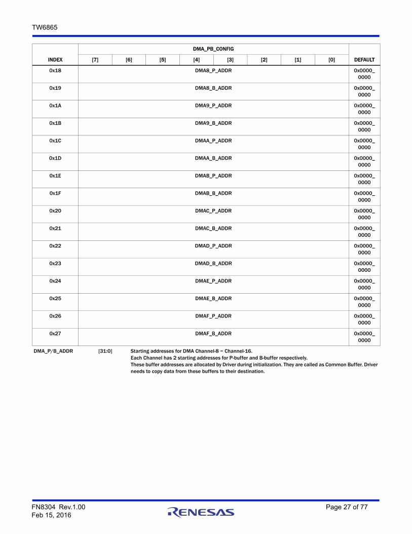
DMA_P/B_ADDR [31:0] Starting addresses for DMA Channel-8 ~ Channel-16. Each Channel has 2 starting addresses for P-buffer and B-buffer respectively.These buffer addresses are allocated by Driver during initialization. They are called as Common Buffer. Driver needs to copy data from these buffers to their destination.
FN8304 Rev.1.00 Page 27 of 77Feb 15, 2016

TW6865
INDEX
VIDEO_CONTROL1
DEFAULT[7] [6] [5] [4] [3] [2] [1] [0]
0x2A B3 0 0 0 0 0 0 0 0 0x00
B2 0 0 0 0 0 0 0 SYS_MODE_DMA3
0x00
B1 SYS_MODE_DMA2
SYS_MODE_DMA1
SYS_MODE_DMA0
0 0 VSCL_ENA_1
0 0 0x00
B0 HSCL_ENA_0
VSCL_ENA_0
0 0 0 0 0 0 0x01
SYS_MODE_DMA3 B[16] System mode for DMA Channel-30 = 525 Lines 1 = 625 Lines
SYS_MODE_DMA2 B[15] System mode for DMA Channel-2SYS_MODE_DMA1 B[14] System mode for DMA Channel-1SYS_MODE_DMA0 B[13] System mode for DMA Channel-0
B[10] set the input format of DMA Channel-4 ~ Channel-7.VSCL_ENA_1 B[10] Vertical scaler
0 = Disabled1 = Enabled (360x240)
B[7:6] set the input format of DMA Channel-0~Channel-3.HSCL_ENA_0 B[7] Horizontal scaler
0 = Disabled (full D1)1 = Enable – 360x480(B[6] = 0) or 360x240(B[6] = 1)
VSCL_ENA_0 B[6] Vertical scaler 0 = Disabled1 = Enabled (360x240) -- B[7] must be “1”
FN8304 Rev.1.00 Page 28 of 77Feb 15, 2016
TW6865
INDEX
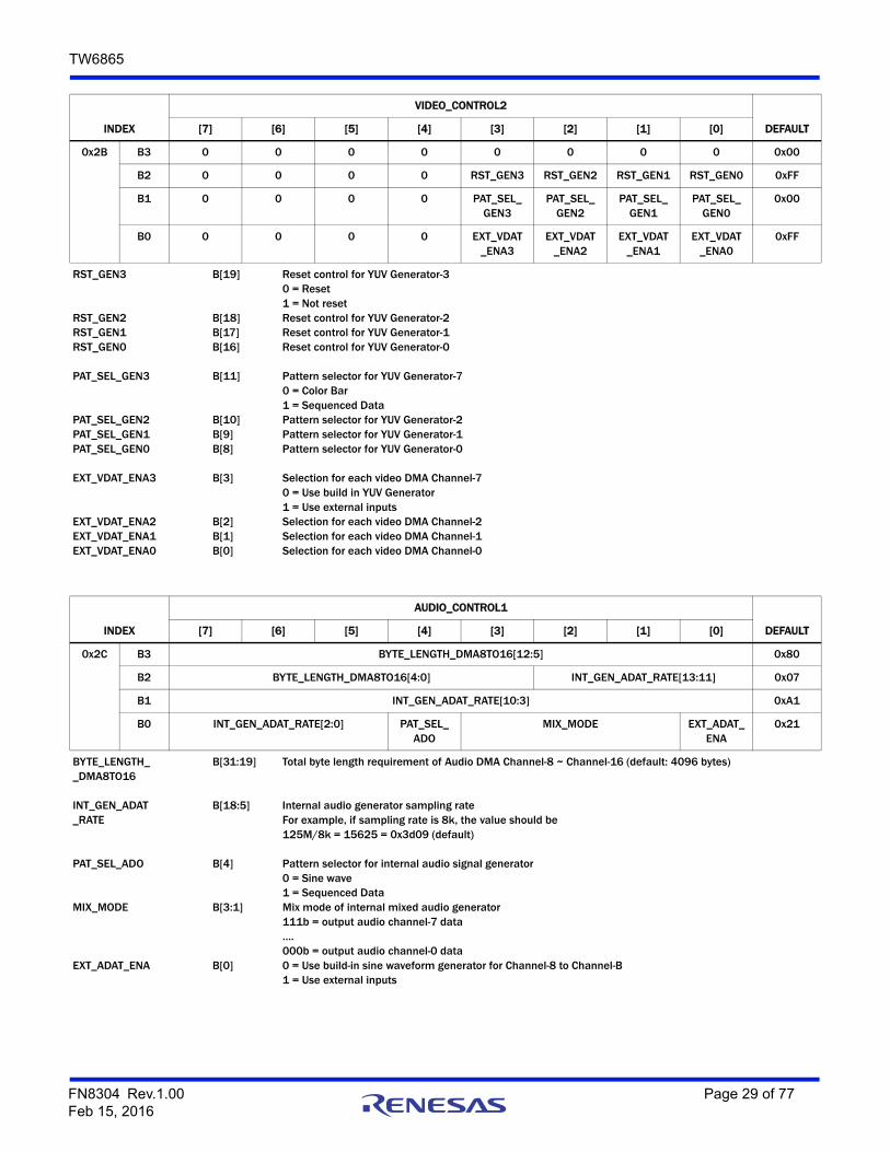
VIDEO_CONTROL2
DEFAULT[7] [6] [5] [4] [3] [2] [1] [0]
0x2B B3 0 0 0 0 0 0 0 0 0x00
B2 0 0 0 0 RST_GEN3 RST_GEN2 RST_GEN1 RST_GEN0 0xFF
B1 0 0 0 0 PAT_SEL_GEN3
PAT_SEL_GEN2
PAT_SEL_GEN1
PAT_SEL_GEN0
0x00
B0 0 0 0 0 EXT_VDAT_ENA3
EXT_VDAT_ENA2
EXT_VDAT_ENA1
EXT_VDAT_ENA0
0xFF
RST_GEN3 B[19] Reset control for YUV Generator-30 = Reset1 = Not reset
RST_GEN2 B[18] Reset control for YUV Generator-2RST_GEN1 B[17] Reset control for YUV Generator-1RST_GEN0 B[16] Reset control for YUV Generator-0
PAT_SEL_GEN3 B[11] Pattern selector for YUV Generator-70 = Color Bar1 = Sequenced Data
PAT_SEL_GEN2 B[10] Pattern selector for YUV Generator-2PAT_SEL_GEN1 B[9] Pattern selector for YUV Generator-1PAT_SEL_GEN0 B[8] Pattern selector for YUV Generator-0
EXT_VDAT_ENA3 B[3] Selection for each video DMA Channel-70 = Use build in YUV Generator1 = Use external inputs
EXT_VDAT_ENA2 B[2] Selection for each video DMA Channel-2EXT_VDAT_ENA1 B[1] Selection for each video DMA Channel-1EXT_VDAT_ENA0 B[0] Selection for each video DMA Channel-0
INDEX
AUDIO_CONTROL1
DEFAULT[7] [6] [5] [4] [3] [2] [1] [0]
0x2C B3 BYTE_LENGTH_DMA8TO16[12:5] 0x80
B2 BYTE_LENGTH_DMA8TO16[4:0] INT_GEN_ADAT_RATE[13:11] 0x07
B1 INT_GEN_ADAT_RATE[10:3] 0xA1
B0 INT_GEN_ADAT_RATE[2:0] PAT_SEL_ADO
MIX_MODE EXT_ADAT_ENA
0x21
BYTE_LENGTH_ B[31:19] Total byte length requirement of Audio DMA Channel-8 ~ Channel-16 (default: 4096 bytes)_DMA8TO16
INT_GEN_ADAT B[18:5] Internal audio generator sampling rate _RATE For example, if sampling rate is 8k, the value should be
125M/8k = 15625 = 0x3d09 (default)
PAT_SEL_ADO B[4] Pattern selector for internal audio signal generator0 = Sine wave1 = Sequenced Data
MIX_MODE B[3:1] Mix mode of internal mixed audio generator111b = output audio channel-7 data….000b = output audio channel-0 data
EXT_ADAT_ENA B[0] 0 = Use build-in sine waveform generator for Channel-8 to Channel-B1 = Use external inputs
FN8304 Rev.1.00 Page 29 of 77Feb 15, 2016

TW6865
INDEX
AUDIO_CONTROL2
DEFAULT[7] [6] [5] [4] [3] [2] [1] [0]
0x2D B3 0 0 AUDIO_CLK_REF[29:24] 0x3D
B2 AUDIO_CLK_REF[23:0] 0x09
B1 0x00
B0 0x00
AUDIO_CLK_REF B[29:0] Audio sampling frequency referenceA_ref = (224)*125MHz/(256*Fs)
---------------------------------------------------------Sampling Rate Value (kHz) (HEX)---------------------------------------------------------8 0x3D09_000016 0x1E84_800032 0x0F42_400044.1 0x0B12_779548 0x0A2C_2AAA---------------------------------------------------------
INDEX
PHASE_REF
DEFAULT[7] [6] [5] [4] [3] [2] [1] [0]
0x2E B3 0 0 0 0 0x00
B2 DMA_MODE3 DMA_MODE2 DMA_MODE1 DMA_MODE0 0x00
B1 0 0 PHASE_REF[13:8] 0x14
B0 PHASE_REF[7:0] 0x4D
DMA_MODE3 B[23:22] DMA mode configuration of DMA Channel-300b = S and G mode01b = Reserved10b = Frame mode11b = Field mode
DMA_MODE2 B[21:20] DMA mode configuration of DMA Channel-2DMA_MODE1 B[19:18] DMA mode configuration of DMA Channel-1DMA_MODE0 B[17:16] DMA mode configuration of DMA Channel-0
PHASE_REF B[13:0] Phase reference for rate conversion at each video DMA channel. Valid range is [4800:5400]
FN8304 Rev.1.00 Page 30 of 77Feb 15, 2016
TW6865
INDEX
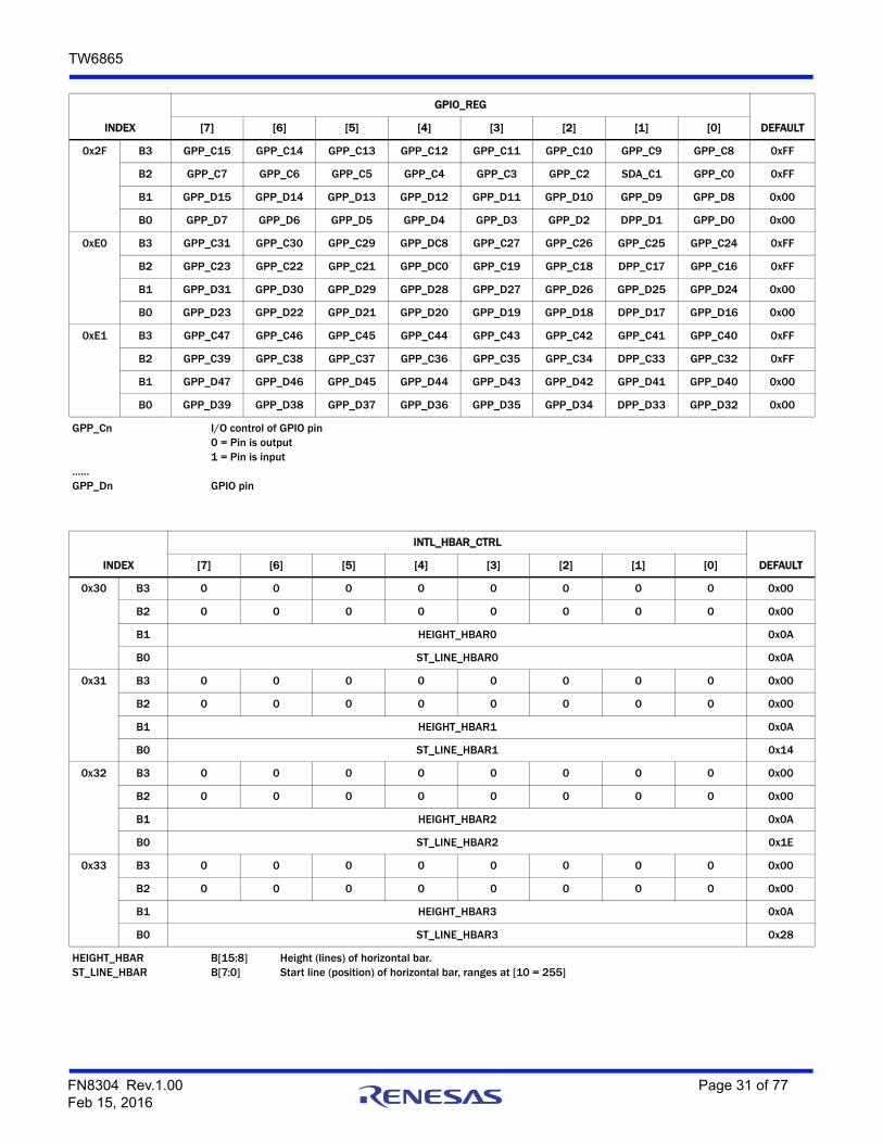
GPIO_REG
DEFAULT[7] [6] [5] [4] [3] [2] [1] [0]
0x2F B3 GPP_C15 GPP_C14 GPP_C13 GPP_C12 GPP_C11 GPP_C10 GPP_C9 GPP_C8 0xFF
B2 GPP_C7 GPP_C6 GPP_C5 GPP_C4 GPP_C3 GPP_C2 SDA_C1 GPP_C0 0xFF
B1 GPP_D15 GPP_D14 GPP_D13 GPP_D12 GPP_D11 GPP_D10 GPP_D9 GPP_D8 0x00
B0 GPP_D7 GPP_D6 GPP_D5 GPP_D4 GPP_D3 GPP_D2 DPP_D1 GPP_D0 0x00
0xE0 B3 GPP_C31 GPP_C30 GPP_C29 GPP_DC8 GPP_C27 GPP_C26 GPP_C25 GPP_C24 0xFF
B2 GPP_C23 GPP_C22 GPP_C21 GPP_DC0 GPP_C19 GPP_C18 DPP_C17 GPP_C16 0xFF
B1 GPP_D31 GPP_D30 GPP_D29 GPP_D28 GPP_D27 GPP_D26 GPP_D25 GPP_D24 0x00
B0 GPP_D23 GPP_D22 GPP_D21 GPP_D20 GPP_D19 GPP_D18 DPP_D17 GPP_D16 0x00
0xE1 B3 GPP_C47 GPP_C46 GPP_C45 GPP_C44 GPP_C43 GPP_C42 GPP_C41 GPP_C40 0xFF
B2 GPP_C39 GPP_C38 GPP_C37 GPP_C36 GPP_C35 GPP_C34 DPP_C33 GPP_C32 0xFF
B1 GPP_D47 GPP_D46 GPP_D45 GPP_D44 GPP_D43 GPP_D42 GPP_D41 GPP_D40 0x00
B0 GPP_D39 GPP_D38 GPP_D37 GPP_D36 GPP_D35 GPP_D34 DPP_D33 GPP_D32 0x00
GPP_Cn I/O control of GPIO pin0 = Pin is output1 = Pin is input
……GPP_Dn GPIO pin
INDEX
INTL_HBAR_CTRL
DEFAULT[7] [6] [5] [4] [3] [2] [1] [0]
0x30 B3 0 0 0 0 0 0 0 0 0x00
B2 0 0 0 0 0 0 0 0 0x00
B1 HEIGHT_HBAR0 0x0A
B0 ST_LINE_HBAR0 0x0A
0x31 B3 0 0 0 0 0 0 0 0 0x00
B2 0 0 0 0 0 0 0 0 0x00
B1 HEIGHT_HBAR1 0x0A
B0 ST_LINE_HBAR1 0x14
0x32 B3 0 0 0 0 0 0 0 0 0x00
B2 0 0 0 0 0 0 0 0 0x00
B1 HEIGHT_HBAR2 0x0A
B0 ST_LINE_HBAR2 0x1E
0x33 B3 0 0 0 0 0 0 0 0 0x00
B2 0 0 0 0 0 0 0 0 0x00
B1 HEIGHT_HBAR3 0x0A
B0 ST_LINE_HBAR3 0x28
HEIGHT_HBAR B[15:8] Height (lines) of horizontal bar.ST_LINE_HBAR B[7:0] Start line (position) of horizontal bar, ranges at [10 = 255]
FN8304 Rev.1.00 Page 31 of 77Feb 15, 2016

TW6865
INDEX
AUDIO_CONTROL3
DEFAULT[7] [6] [5] [4] [3] [2] [1] [0]
0x38 B3 0 0 0 0 0 0 0 0 0x00
B2 0 0 0 0 0 0 0 0 0x00
B1 0 0 0 0 0 0 0 OUT_BITWIDTH
0x00
B0 0 0 0 0 0 0 0 0 0x40
OUT_BITWIDTH B[8] Audio DMA output bit width0 = 16 bits1 = 8 bits
INDEX
VIDEO_FIELD_CTRL
DEFAULT[7] [6] [5] [4] [3] [2] [1] [0]
0x39 B3 FLD_CTRL_ENA0
START_FLD0
FLD_OUT_OPT0[29:24] 0x00
B2 FLD_OUT_OPT0[23:0] 0x00
B1 0x00
B0 0x00
0x3A B3 FLD_CTRL_ENA1
START_FLD1
FLD_OUT_OPT1[29:24] 0x00
B2 FLD_OUT_OPT1[23:0] 0x00
B1 0x00
B0 0x00
0x3B B3 FLD_CTRL_ENA2
START_FLD2
FLD_OUT_OPT2[29:24] 0x00
B2 FLD_OUT_OPT2[23:0] 0x00
B1 0x00
B0 0x00
0x3C B3 FLD_CTRL_ENA3
START_FLD3
FLD_OUT_OPT3[29:24] 0x00
B2 FLD_OUT_OPT3[23:0] 0x00
B1 0x00
B0 0x00
FLD_CTRL_ENA B[31] Enable bit for each field control register0 = Output both odd and even field1 = Output according to B20~B0
START_FLD B[30] Starting field control bit0 = Starting from field 21 = Starting from field 1
FLD_OUT_OPT B[29:0] Output flag of consecutive 30(NTSC)/25(PAL) fields 0 = Not output1 = Output
FN8304 Rev.1.00 Page 32 of 77Feb 15, 2016

TW6865
INDEX
HSCALER_CTRL
DEFAULT[7] [6] [5] [4] [3] [2] [1] [0]
0x42 B3 HSCALER_ENA0
PHASE_REF0[15:9] 0x7C
B2 PHASE_REF0[8:1] 0x71
B1 PHASE_REF0[0]
END_POS0[9:3] 0xD8
B0 END_POS0[2:0] START_POS0 0xCA
0x43 B3 HSCALER_ENA1
PHASE_REF1[15:9] 0x7C
B2 PHASE_REF1[8:1] 0x71
B1 PHASE_REF1[0]
END_POS1[9:3] 0xD8
B0 END_POS1[2:0] START_POS1 0xCA
0x44 B3 HSCALER_ENA2
PHASE_REF2[15:9] 0x7C
B2 PHASE_REF2[8:1] 0x71
B1 PHASE_REF2[0]
END_POS2[9:3] 0xD8
B0 END_POS2[2:0] START_POS2 0xCA
0x45 B3 HSCALER_ENA3
PHASE_REF3[15:9] 0x7C
B2 PHASE_REF3[8:1] 0x71
B1 PHASE_REF3[0]
END_POS3[9:3] 0xD8
B0 END_POS3[2:0] START_POS3 0xCA
HSCALER_ENA B[31] Customize horizontal scaler enable bit0 = Disable1 = Enable
PHASE_REF B[30:15] Scaler phase reference. Its calculation is as follows: Phase_ref = (END_POS–START_POS)*(216)/Total_Active_Pixel_Per_Line
For example, START_POS = 10, END_POS = 710Total_Active_Pixel_Per_Line = 720Phase_ref = (710 - 10)*216/720 = 0xF8E3
END_POS B[14:5] End pixel position of each line. This pixel will NOT be shown and the setting must be an even number.
START_POS B[4:0] Start pixel position of each line. This pixel will be shown and the setting must be an even number.
FN8304 Rev.1.00 Page 33 of 77Feb 15, 2016

TW6865
INDEX
VIDEO_SIZE
DEFAULT[7] [6] [5] [4] [3] [2] [1] [0]
0x4A B3 VS_EN0 VS_F2_EN0 0 0 0 0 0 V_SIZE0[8] 0x00
B2 V_SIZE0[7:0] 0xF0
B1 0 0 0 0 0 H_SIZE0[10:8] 0x02
B0 H_SIZE0[7:0] 0xD0
0x4B B3 VS_EN1 VS_F2_EN1 0 0 0 0 0 V_SIZE1[8] 0x00
B2 V_SIZE1[7:0] 0xF0
B1 0 0 0 0 0 H_SIZE1[10:8] 0x02
B0 H_SIZE1[7:0] 0xD0
0x4C B3 VS_EN2 VS_F2_EN2 0 0 0 0 0 V_SIZE2[8] 0x00
B2 V_SIZE2[7:0] 0xF0
B1 0 0 0 0 0 H_SIZE2[10:8] 0x02
B0 H_SIZE2[7:0] 0xD0
0x4D B3 VS_EN3 VS_F2_EN3 0 0 0 0 0 V_SIZE3[8] 0x00
B2 V_SIZE3[7:0] 0xF0
B1 0 0 0 0 0 H_SIZE3[10:8] 0x02
B0 H_SIZE3[7:0] 0xD0
VS_EN B[31] Customize video size enable bit0 = Disable1 = Enable
VS_F2_EN B[30] Enable to field 2 video size control registers 0 = Field 2 video size controlled byVIDEO_SIZEx 1 = Field 2 video size controlled byVIDEO_SIZEx_F2 Note: “x” means DMA channel number (0 ~ 7)
V_SIZE B[24:16] Height of fieldH_SIZE B[10:0] Width of field
FN8304 Rev.1.00 Page 34 of 77Feb 15, 2016

TW6865
INDEX
VIDEO_SIZE_F2
DEFAULT[7] [6] [5] [4] [3] [2] [1] [0]
0x52 B3 0 0 0 0 0 0 0 V_SIZE0_F2[8]
0x00
B2 V_SIZE0_F2[7:0] 0xF0
B1 0 0 0 0 0 H_SIZE0_F2[10:8] 0x02
B0 H_SIZE0_F2[7:0] 0xD0
0x53 B3 0 0 0 0 0 0 0 V_SIZE1_F2[8]
0x00
B2 V_SIZE1_F2[7:0] 0xF0
B1 0 0 0 0 0 H_SIZE1_F2[10:8] 0x02
B0 H_SIZE1_F2[7:0] 0xD0
0x54 B3 0 0 0 0 0 0 0 V_SIZE2_F2[8]
0x00
B2 V_SIZE2_F2[7:0] 0xF0
B1 0 0 0 0 0 H_SIZE2_F2[10:8] 0x02
B0 H_SIZE2_F2[7:0] 0xD0
0x55 B3 0 0 0 0 0 0 0 V_SIZE3_F2[8]
0x00
B2 V_SIZE3_F2[7:0] 0xF0
B1 0 0 0 0 0 H_SIZE3_F2[10:8] 0x02
B0 H_SIZE3_F2[7:0] 0xD0
V_SIZE_F2 B[24:16] Height of field 2H_SIZE_F2 B[10:0] Width of field 2
FN8304 Rev.1.00 Page 35 of 77Feb 15, 2016

TW6865
INDEX
MD_CONF
DEFAULT[7] [6] [5] [4] [3] [2] [1] [0]
0x60 B3 0 0 0 0 0 0 0 0 0x00
B2 MD0_TSCALE MD0_ENABLE
MD0_ACT_FLD
MD0_MODE MD0_THRESHOLD[17:16] 0x05
B1 MD0_THRESHOLD[15:8] 0x04
B0 MD0_THRESHOLD[7:0] 0x10
0x61 B3 0 0 0 0 0 0 0 0 0x00
B2 MD1_TSCALE MD1_ENABLE
MD1_ACT_FLD
MD1_MODE MD1_THRESHOLD[17:16] 0x05
B1 MD1_THRESHOLD[15:8] 0x04
B0 MD1_THRESHOLD[7:0] 0x10
0x62 B3 0 0 0 0 0 0 0 0 0x00
B2 MD2_TSCALE MD2_ENABLE
MD2_ACT_FLD
MD2_MODE MD2_THRESHOLD[17:16] 0x05
B1 MD2_THRESHOLD[15:8] 0x04
B0 MD2_THRESHOLD[7:0] 0x10
0x63 B3 0 0 0 0 0 0 0 0 0x00
B2 MD3_TSCALE MD3_ENABLE
MD3_ACT_FLD
MD3_MODE MD3_THRESHOLD[17:16] 0x05
B1 MD3_THRESHOLD[15:8] 0x04
B0 MD3_THRESHOLD[7:0] 0x10
MD_TSCALE B[23:21] Scale amount of threshold (T<<TSCALE)MD_ENABLE B[20] Enable Motion Detection
0 = Disable1 = Enable
MD_ACT_FLD B [19] Motion Detection Active Field0 = Field 01 = Field 1
MD_MODE B [18] Motion Detection Block Size0 = Block size is 16x161 = Block size is 32x32
MD_TRESHOLD B[17:0] Threshold for Motion or Static
FN8304 Rev.1.00 Page 36 of 77Feb 15, 2016

TW6865
INDEX
MD_INIT
DEFAULT[7] [6] [5] [4] [3] [2] [1] [0]
0x68 B3 0 0 0 0 0 0 0 0 0x00
B2 0 0 0 0 0 0 0 0 0x00
B1 0 0 0 0 0 0 0 0 0x00
B0 0 0 0 0 0 0 0 MD0_INIT 0x00
0x69 B3 0 0 0 0 0 0 0 0 0x00
B2 0 0 0 0 0 0 0 0 0x00
B1 0 0 0 0 0 0 0 0 0x00
B0 0 0 0 0 0 0 0 MD1_INIT 0x00
0x6A B3 0 0 0 0 0 0 0 0 0x00
B2 0 0 0 0 0 0 0 0 0x00
B1 0 0 0 0 0 0 0 0 0x00
B0 0 0 0 0 0 0 0 MD2_INIT 0x00
0x6B B3 0 0 0 0 0 0 0 0 0x00
B2 0 0 0 0 0 0 0 0 0x00
B1 0 0 0 0 0 0 0 0 0x00
B0 0 0 0 0 0 0 0 MD3_INIT 0x00
MD_INIT B[0] Motion Detection Read Pointer Initialization. By writing any value to it, the read pointer will be reset.
INDEX
MD_MAPO
DEFAULT[7] [6] [5] [4] [3] [2] [1] [0]
0x70 B3 0 0 0 0 0 0 0 0 0x00
B2 MD0_MAPO[23:16] 0x00
B1 MD0_MAPO[15:8] 0x00
B0 MD0_MAPO[7:0] 0x00
0x71 B3 0 0 0 0 0 0 0 0 0x00
B2 MD1_MAPO[23:16] 0x00
B1 MD1_MAPO[15:8] 0x00
B0 MD1_MAPO[7:0] 0x00
0x72 B3 0 0 0 0 0 0 0 0 0x00
B2 MD2_MAPO[23:16] 0x00
B1 MD2_MAPO[15:8] 0x00
B0 MD2_MAPO[7:0] 0x00
0x73 B3 0 0 0 0 0 0 0 0 0x00
B2 MD3_MAPO[23:16] 0x00
B1 MD3_MAPO[15:8] 0x00
B0 MD3_MAPO[7:0] 0x00
MD_MAPO B[23:0] Map of motion detection output for blocks of current slice.Note: Video frame is partitioned into multiple slices (number of vertical blocks). After MD_INIT, the output of first slice will be read through one register read operation and read pointer will be moved to the next slice. Host can issue read command until all the slices have been read. MD_MAPO[0] maps to the first block in current slice.
FN8304 Rev.1.00 Page 37 of 77Feb 15, 2016

TW6865
INDEX
ADDR_P_DMA
DEFAULT[7] [6] [5] [4] [3] [2] [1] [0]
0x80 B3 ADDR_P_DMA0 0x00
B2 0x00
B1 0x00
B0 0x00
0x88 B3 ADDR_P_DMA1 0x00
B2 0x00
B1 0x00
B0 0x00
0x90 B3 ADDR_P_DMA2 0x00
B2 0x00
B1 0x00
B0 0x00
0x98 B3 ADDR_P_DMA3 0x00
B2 0x00
B1 0x00
B0 0x00
ADDR_P_DMA B[31:0] Start address of P-buffer for DMA Channel-0 ~ Channel-3.
INDEX
WHP_DMA
DEFAULT[7] [6] [5] [4] [3] [2] [1] [0]
0x81 B3 HEIGHT0[9:2] 0x3C
B2 HEIGHT0[1:0] LINE_WIDTH0[10:5] 0x2E
B1 LINE_WIDTH0 [4:0] ACTIVE_WIDTH0[10:8] 0xA5
B0 ACTIVE_WIDTH0[7:0] 0xA0
0x89 B3 HEIGHT1[9:2] 0x3C
B2 HEIGHT1[1:0] LINE_WIDTH1[10:5] 0x2E
B1 LINE_WIDTH1[4:0] ACTIVE_WIDTH1[10:8] 0xA5
B0 ACTIVE_WIDTH1[7:0] 0xA0
0x91 B3 HEIGHT2[9:2] 0x3C
B2 HEIGHT2[1:0] LINE_WIDTH2[10:5] 0x2E
B1 LINE_WIDTH2[4:0] ACTIVE_WIDTH2[10:8] 0xA5
B0 ACTIVE_WIDTH2[7:0] 0xA0
0x99 B3 HEIGHT3[9:2] 0x3C
B2 HEIGHT3[1:0] LINE_WIDTH3[10:5] 0x2E
B1 LINE_WIDTH3[4:0] ACTIVE_WIDTH3[10:8] 0xA5
B0 ACTIVE_WIDTH3[7:0] 0xA0
For DMA Channel-0~Channel-3:HEIGHT B[31:22] Total active lines LINE_WIDTH B[21:11] Total bytes per line ACTIVE_WIDTH B[10:0] Total active bytes per line
FN8304 Rev.1.00 Page 38 of 77Feb 15, 2016

TW6865
INDEX
ADDR_B_DMA
DEFAULT[7] [6] [5] [4] [3] [2] [1] [0]
0x82 B3 ADDR_B_DMA0 0x00
B2 0x00
B1 0x00
B0 0x00
0x8A B3 ADDR_B_DMA1 0x00
B2 0x00
B1 0x00
B0 0x00
0x92 B3 ADDR_B_DMA2 0x00
B2 0x00
B1 0x00
B0 0x00
ADDR_B_DMA B[31:0] Start address of B-buffer for DMA Channel-0 ~ Channel-3
INDEX
F2_ADDR_P_DMA
DEFAULT[7] [6] [5] [4] [3] [2] [1] [0]
0x84 B3 F2_ADDR_P_DMA0 0x00
B2 0x00
B1 0x00
B0 0x00
0x8C B3 F2_ADDR_P_DMA1 0x00
B2 0x00
B1 0x00
B0 0x00
0x94 B3 F2_ADDR_P_DMA2 0x00
B2 0x00
B1 0x00
B0 0x00
0x9C B3 F2_ADDR_P_DMA3 0x00
B2 0x00
B1 0x00
B0 0x00
F2_ADDR_P_DMA B[31:0] Start address of Field 2 P-buffer for DMA Channel-0 ~ Channel-3
FN8304 Rev.1.00 Page 39 of 77Feb 15, 2016

TW6865
INDEX
F2_WHP_DMA
DEFAULT[7] [6] [5] [4] [3] [2] [1] [0]
0x85 B3 F2_HEIGHT0[9:2] 0x3C
B2 F2_HEIGHT0[1:0] F2_LINE_WIDTH0[10:5] 0x2E
B1 F2_LINE_WIDTH0 [4:0] F2_ACTIVE_WIDTH0[10:8] 0xA5
B0 F2_ACTIVE_WIDTH0[7:0] 0xA0
0x8D B3 F2_HEIGHT1[9:2] 0x3C
B2 F2_HEIGHT1[1:0] F2_LINE_WIDTH1[10:5] 0x2E
B1 F2_LINE_WIDTH1[4:0] F2_ACTIVE_WIDTH1[10:8] 0xA5
B0 F2_ACTIVE_WIDTH1[7:0] 0xA0
0x95 B3 F2_HEIGHT2[9:2] 0x3C
B2 F2_HEIGHT2[1:0] F2_LINE_WIDTH2[10:5] 0x2E
B1 F2_LINE_WIDTH2[4:0] F2_ACTIVE_WIDTH2[10:8] 0xA5
B0 F2_ACTIVE_WIDTH2[7:0] 0xA0
0x9D B3 F2_HEIGHT3[9:2] 0x3C
B2 F2_HEIGHT3[1:0] F2_LINE_WIDTH3[10:5] 0x2E
B1 F2_LINE_WIDTH3[4:0] F2_ACTIVE_WIDTH3[10:8] 0xA5
B0 F2_ACTIVE_WIDTH3[7:0] 0xA0
For DMA Channel-0~Channel-3:F2_HEIGHT B[31:22] Total active lines in field 2F2_LINE_WIDTH B[21:11] Total bytes per line in field 2F2_ACTIVE_WIDTH B[10:0] Total active bytes per line in field 2
INDEX
F2_ADDR_B_DMA
DEFAULT[7] [6] [5] [4] [3] [2] [1] [0]
0x86 B3 F2_ADDR_B_DMA0 0x00
B2 0x00
B1 0x00
B0 0x00
0x8E B3 F2_ADDR_B_DMA1 0x00
B2 0x00
B1 0x00
B0 0x00
0x96 B3 F2_ADDR_B_DMA2 0x00
B2 0x00
B1 0x00
B0 0x00
0x9E B3 F2_ADDR_B_DMA3 0x00
B2 0x00
B1 0x00
B0 0x00
F2_ADDR_P_DMA B[31:0] Start address of Field 2 B-buffer for DMA Channel-0 ~ Channel-3.
FN8304 Rev.1.00 Page 40 of 77Feb 15, 2016
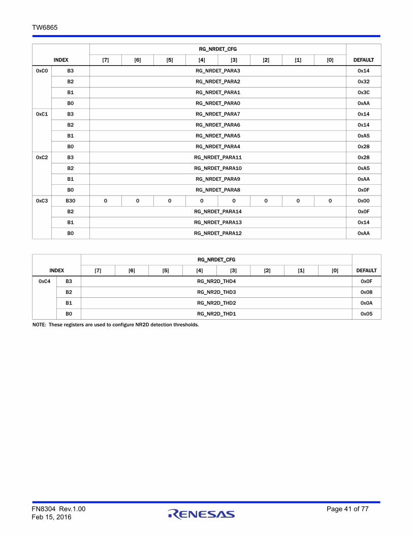
TW6865
INDEX
RG_NRDET_CFG
DEFAULT[7] [6] [5] [4] [3] [2] [1] [0]
0xC0 B3 RG_NRDET_PARA3 0x14
B2 RG_NRDET_PARA2 0x32
B1 RG_NRDET_PARA1 0x3C
B0 RG_NRDET_PARA0 0xAA
0xC1 B3 RG_NRDET_PARA7 0x14
B2 RG_NRDET_PARA6 0x14
B1 RG_NRDET_PARA5 0xA5
B0 RG_NRDET_PARA4 0x28
0xC2 B3 RG_NRDET_PARA11 0x28
B2 RG_NRDET_PARA10 0xA5
B1 RG_NRDET_PARA9 0xAA
B0 RG_NRDET_PARA8 0x0F
0xC3 B30 0 0 0 0 0 0 0 0 0x00
B2 RG_NRDET_PARA14 0x0F
B1 RG_NRDET_PARA13 0x14
B0 RG_NRDET_PARA12 0xAA
INDEX
RG_NRDET_CFG
DEFAULT[7] [6] [5] [4] [3] [2] [1] [0]
0xC4 B3 RG_NR2D_THD4 0x0F
B2 RG_NR2D_THD3 0x08
B1 RG_NR2D_THD2 0x0A
B0 RG_NR2D_THD1 0x05
NOTE: These registers are used to configure NR2D detection thresholds.
FN8304 Rev.1.00 Page 41 of 77Feb 15, 2016

TW6865
INDEX
RG_NR_CTRL
DEFAULT[7] [6] [5] [4] [3] [2] [1] [0]
0xC8 B3 0 0 0 0 0 0 0 0 0x00
B2 NR2D_ENA0 SKIP_CNT1 SKIP_CNT0 RGA_RST_NRDET0
RG_NRDET_CTL0 0x00
B1 RG_FRONT_GEN_CTL0 0x00
B0 RG_FRONT_CTL0 0x00
0xC9 B3 0 0 0 0 0 0 0 0 0x00
B2 NR2D_ENA1 0 0 RGA_RST_NRDET1
RG_NRDET_CTL1 0x00
B1 RG_FRONT_GEN_CTL1 0x00
B0 RG_FRONT_CTL1 0x00
0xCA B3 0 0 0 0 0 0 0 0 0x00
B2 NR2D_ENA2 0 0 RGA_RST_NRDET2
RG_NRDET_CTL2 0x00
B1 RG_FRONT_GEN_CTL2 0x00
B0 RG_FRONT_CTL2 0x00
0xCB B3 0 0 0 0 0 0 0 0 0x00
B2 NR2D_ENA3 0 0 RGA_RST_NRDET3
RG_NRDET_CTL3 0x00
B1 RG_FRONT_GEN_CTL3 0x00
B0 RG_FRONT_CTL3 0x00
NR2D_ENA B[23] Enable 2D noise reduction0 = Disable1 = Enable
SKIP_CNT[1:0] B[22:21] Define how many fields to be skipped before processing.RGA_RST_NRDET B [20] Reset noise detectionRG_NRDET_CTL B [19:16] Noise detection controlRG_FRONT_GEN_CTL B [15:8] Front controlRG_FRONT_CTL B [7:0] Front gen control
FN8304 Rev.1.00 Page 42 of 77Feb 15, 2016
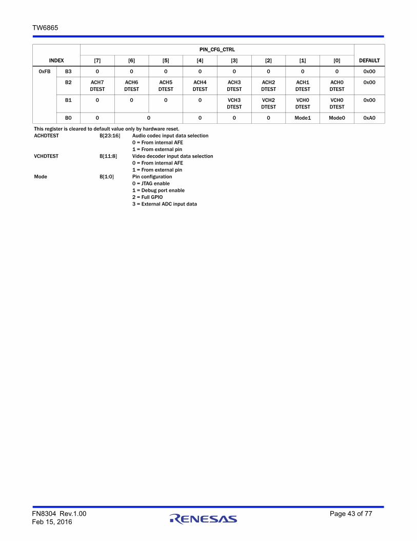
TW6865
INDEX
PIN_CFG_CTRL
DEFAULT[7] [6] [5] [4] [3] [2] [1] [0]
0xFB B3 0 0 0 0 0 0 0 0 0x00
B2 ACH7DTEST
ACH6DTEST
ACH5DTEST
ACH4DTEST
ACH3DTEST
ACH2DTEST
ACH1DTEST
ACH0DTEST
0x00
B1 0 0 0 0 VCH3DTEST
VCH2DTEST
VCH0DTEST
VCH0DTEST
0x00
B0 0 0 0 0 0 Mode1 Mode0 0xA0
This register is cleared to default value only by hardware reset.ACHDTEST B[23:16] Audio codec input data selection
0 = From internal AFE1 = From external pin
VCHDTEST B[11:8] Video decoder input data selection0 = From internal AFE1 = From external pin
Mode B[1:0] Pin configuration0 = JTAG enable1 = Debug port enable2 = Full GPIO 3 = External ADC input data
FN8304 Rev.1.00 Page 43 of 77Feb 15, 2016

TW6865
INDEX
DBGPORT_CTRL
DEFAULT[7] [6] [5] [4] [3] [2] [1] [0]
0xFC B3 0 0 0 0 0 0 0 0 0x00
B2 0 0 0 0 0 0 0 0 0x00
B1 MSB16_EN BLOCK_SEL 0x00
B0 SUBMODULE_SEL 0x00
MSB16_EN B[15] Enable MSB 16 bits of debug signal at output ports0 = Disable (so that LSB 16 bits are wired to ports)1 = Enable
BLOCK_SEL B[14:8] Block selection for debug port outputSUBMODULE_SEL B[7:0] Sub-module of block selection
BLOCK_SEL SUBMODULE_SEL DEBUG PORTS
0 0x0 PIPE Interface
0x1 PCIE EndPoint
0x2 PCIE EndPoint
0x3 Status of DMA Parser
0x4 I2S Receiver
1 0x0 DMA_CH0
0x1 DMA_CH1
0x2 DMA_CH2
0x3 DMA_CH3
0x4 Reserved
0x5 Reserved
0x6 Reserved
0x7 Reserved
0x8 DMA_CH8
0x9 DMA_CH9
0xA DMA_CH10
0xB DMA_CH11
0xC DMA_CH12
0xD DMA_CH13
0xE DMA_CH14
0xF DMA_CH15
0x10 Schedule
0x11 MSI
0x12 Client
0x13 Cpl
0x14 DMA_CH16
2 0x0 Parser1
0x1 Parser2
0x2 Parser3
0x3 Parser4
0x4 Parser5
0x5 Parser6
0x6 Parser7
0x7 Parser8
FN8304 Rev.1.00 Page 44 of 77Feb 15, 2016
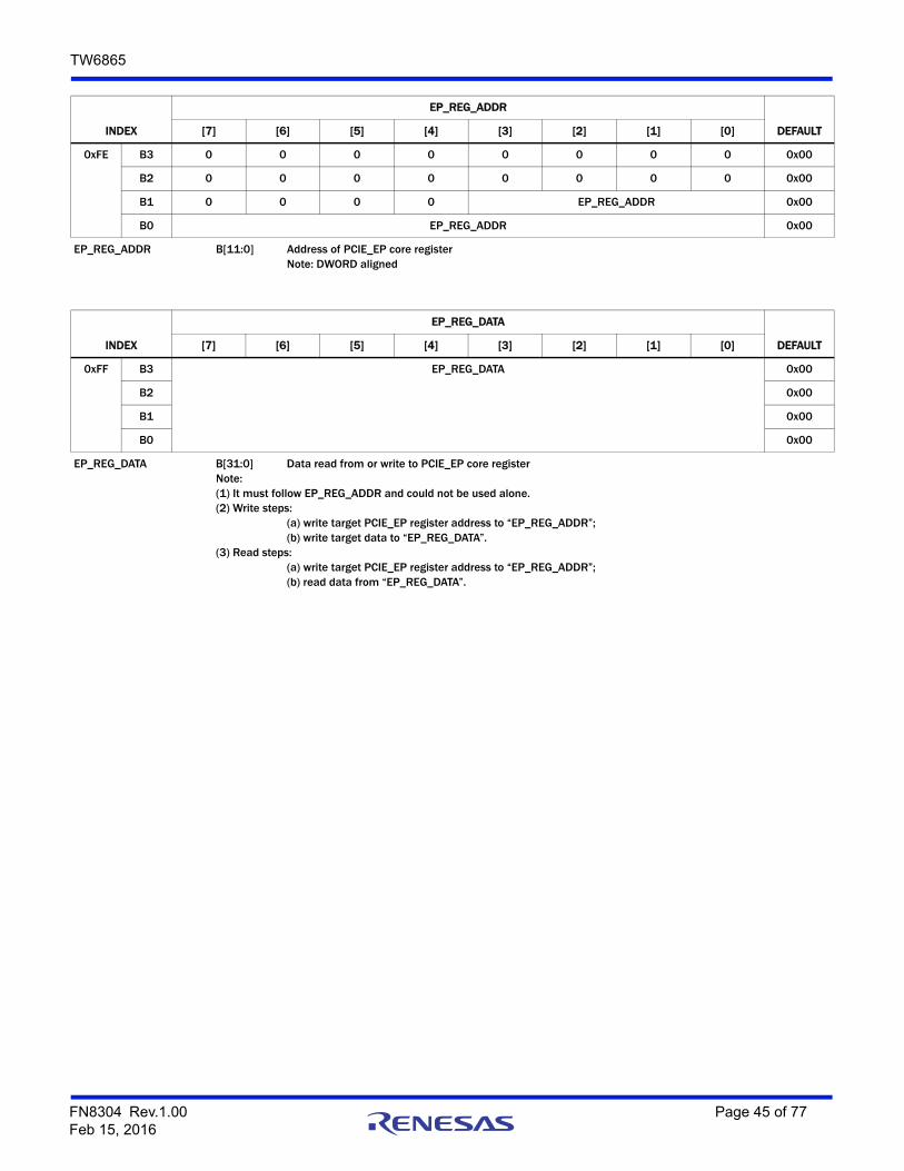
TW6865
INDEX
EP_REG_ADDR
DEFAULT[7] [6] [5] [4] [3] [2] [1] [0]
0xFE B3 0 0 0 0 0 0 0 0 0x00
B2 0 0 0 0 0 0 0 0 0x00
B1 0 0 0 0 EP_REG_ADDR 0x00
B0 EP_REG_ADDR 0x00
EP_REG_ADDR B[11:0] Address of PCIE_EP core register Note: DWORD aligned
INDEX
EP_REG_DATA
DEFAULT[7] [6] [5] [4] [3] [2] [1] [0]
0xFF B3 EP_REG_DATA 0x00
B2 0x00
B1 0x00
B0 0x00
EP_REG_DATA B[31:0] Data read from or write to PCIE_EP core registerNote: (1) It must follow EP_REG_ADDR and could not be used alone.(2) Write steps:
(a) write target PCIE_EP register address to “EP_REG_ADDR”;(b) write target data to “EP_REG_DATA”.
(3) Read steps: (a) write target PCIE_EP register address to “EP_REG_ADDR”;(b) read data from “EP_REG_DATA”.
FN8304 Rev.1.00 Page 45 of 77Feb 15, 2016

TW6865
Video Decoder AND Audio Codec (CH0 ~ CH3)(Starting from 0x100) (B[31:8] are hardwired to 0 in all registers)
INDEX VIDEO STATUS REGISTER
DEFAULTCH1 CH2 CH3 CH4 [7] [6] [5] [4] [3] [2] [1] [0]
0x100 0x110 0x120 0x130 VDLOSS HLOCK SLOCK FIELD VLOCK 0 MONO DET50 0x00
VDLOSS B[7] 1 = Video not present. (sync is not detected in number of consecutive line periods specified by MISSCNT register)0 = Video detected
HLOCK B[6] 1 = Horizontal sync PLL is locked to the incoming video source0 = Horizontal sync PLL is not locked
SLOCK B[5] 1 = Subcarrier PLL is locked to the incoming video source0 = Subcarrier PLL is not locked
FIELD B[4] 0 = Odd field is being decoded1 = Even field is being decoded
VLOCK B[3] 1 = Vertical logic is locked to the incoming video source0 = Vertical logic is not locked
MONO B[1] 1 = No color burst signal detected0 = Color burst signal detected
DET50 B[0] 0 = 60Hz source detected1 = 50Hz source detectedThe actual vertical scanning frequency depends on the current standard invoked.
INDEX BRIGHTNESS CONTROL REGISTER
DEFAULTCH1 CH2 CH3 CH4 [7] [6] [5] [4] [3] [2] [1] [0]
0x101 0x111 0x121 0x131 BRIGHT 0x00
BRIGHT B[7:0] These bits control the brightness. They have value of –128 to 127in 2's complement form. Positive value increases brightness. Avalue 0 has no effect on the data.
INDEX CONTRAST CONTROL REGISTER
DEFAULTCH1 CH2 CH3 CH4 [7] [6] [5] [4] [3] [2] [1] [0]
0x102 0x112 0x122 0x132 CNTRST 0x64
CNTRST B[7:0] These bits control the contrast. They have value of 0 to 3.98 (FFh)A value of 1 (“100_0000”) has not effect on the video data.
INDEX SHARPNESS CONTROL REGISTER
DEFAULTCH1 CH2 CH3 CH4 [7] [6] [5] [4] [3] [2] [1] [0]
0x103 0x113 0x123 0x133 SCURVE VSF CT SHARP 0x11
SCURVE B[7] This bit controls the center frequency of the peaking filter. The corresponding gain adjustment is HFLT.0 = Low1 = Center
VSF B[6] This bit is for internal used.CTI B[5:4] CTI level selection.
0 = None3 = Highest.
SHARP B[3:0] These bits control the amount of sharpness enhancement on the luminance signals. There are 16 levels of control with '0' having no effect on the output image. 1 through 15 provides sharpness enhancement with 'F' being the strongest.
FN8304 Rev.1.00 Page 46 of 77Feb 15, 2016

TW6865
INDEX CHROMA (U) CONTROL REGISTER
DEFAULTCH1 CH2 CH3 CH4 [7] [6] [5] [4] [3] [2] [1] [0]
0x104 0x114 0x124 0x134 SAT_U 0x80
SAT_U B[7:0] These bits control the digital gain adjustment to the U (or Cb)component of the digital video signal. The color saturation can be adjusted by adjusting the U and V color gain components by the same amount in the normal situation. The U and V can also be adjusted independently to provide greater flexibility. The range of adjustment is 0 to 200%.
INDEX CHROMA (V) CONTROL REGISTER
DEFAULTCH1 CH2 CH3 CH4 [7] [6] [5] [4] [3] [2] [1] [0]
0x105 0x115 0x125 0x135 SAT_V 0x80
SAT_V B[7:0] These bits control the digital gain adjustment to the V (or Cr)component of the digital video signal. The color saturation can be adjusted by adjusting the U and V color gain components by the same amount in the normal situation. The U and V can also be adjusted independently to provide greater flexibility. The range of adjustment is 0 to 200%.
INDEX HUE CONTROL REGISTER
DEFAULTCH1 CH2 CH3 CH4 [7] [6] [5] [4] [3] [2] [1] [0]
0x106 0x116 0x126 0x136 HUE 0x00
HUE B[7:0] These bits control the color hue as 2's complement number. They have value from +36° (7Fh) to -36° (80h) with an increment of 0.28°. The positive value gives greenish tone and negative value gives purplish tone. The default value is 0° (00h). This is effective only on NTSC system.
INDEX CROPPING CONTROL REGISTER
DEFAULTCH1 CH2 CH3 CH4 [7] [6] [5] [4] [3] [2] [1] [0]
0x107 0x117 0x127 0x137 VDELAY_HI VACTIVE_HI HDELAY_HI HACTIVE_HI 0x02
VDELAY_HI B[7:6] These bits are Bit 9 to 8 of the 10-bit Vertical Delay register.VACTIVE_HI B[5:4] These bits are Bit 9 to 8 of the 10-bit VACTIVE register. Refer to
description on Reg0x109 for its shadow register.HDELAY_HI B[3:2] These bits are Bit 9 to 8 of the 10-bit Horizontal Delay register.HACTIVE_HI B[1:0] These bits are Bit 9 to 8 of the 10-bit HACTIVE register.
INDEX VERTICAL DELAY REGISTER LOW
DEFAULTCH1 CH2 CH3 CH4 [7] [6] [5] [4] [3] [2] [1] [0]
0x108 0x118 0x128 0x138 VDELAY_LO 0x12
VDELAY_LO B[7:0] These bits are Bit 7 to 0 of the 10-bit Vertical Delay register. The two MSBs are in the CROP_HI register. It defines the number of lines between the leading edge of VSYNC and the start of the active video.
INDEX VERTICAL ACTIVE REGISTER LOW
DEFAULTCH1 CH2 CH3 CH4 [7] [6] [5] [4] [3] [2] [1] [0]
0x109 0x119 0x129 0x139 VACTIVE_LO 0xF0
VACTIVE_LO B[7:0] These bits are Bit 7 to 0 of the 10-bit Vertical Active register. The two MSBs are in the CROP_HI register.It defines the number of active video lines per frame output. The VACTIVE register has a shadow register for use with 50Hz source when ATREG of Reg0x10E/11E/12E/13E is not set. This register can be accessed through the same index address by firstchanging the format standard to any 50Hz standard.
FN8304 Rev.1.00 Page 47 of 77Feb 15, 2016
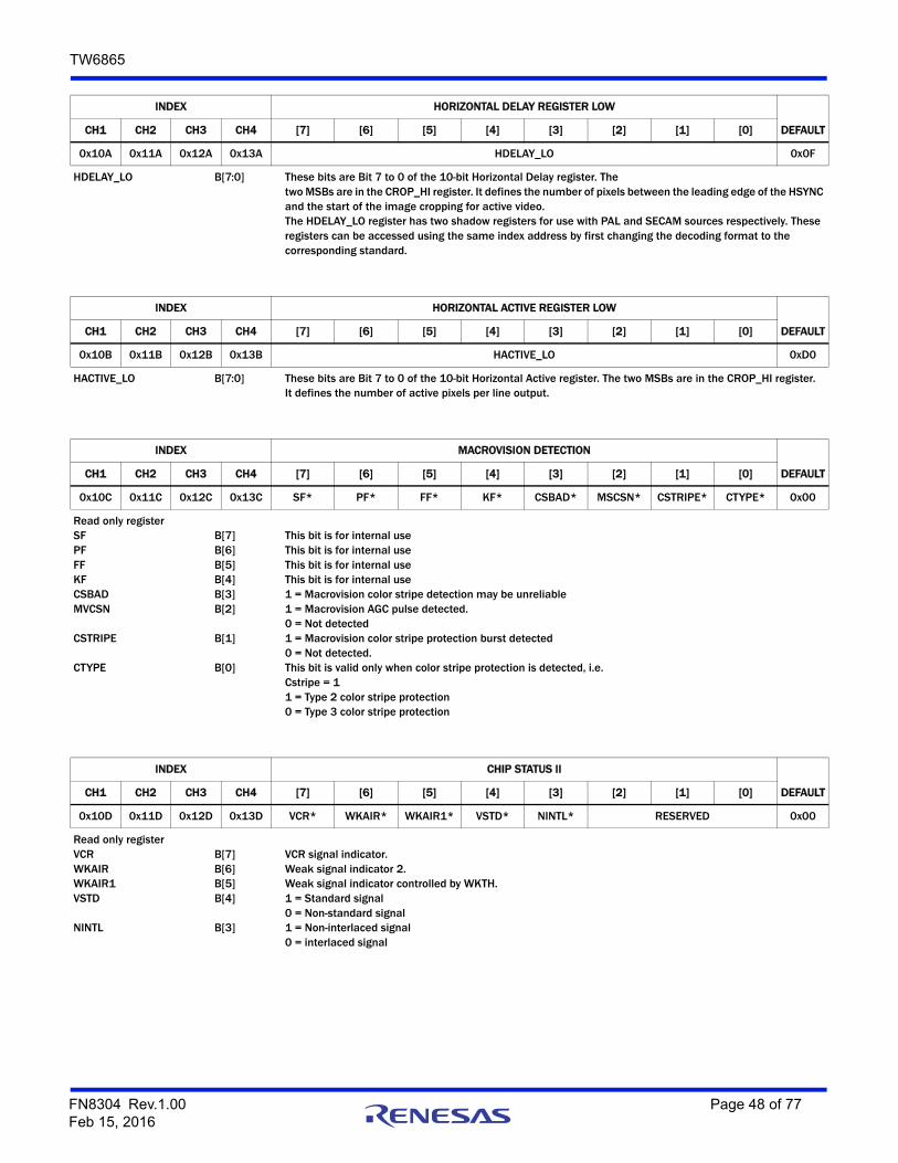
TW6865
INDEX HORIZONTAL DELAY REGISTER LOW
DEFAULTCH1 CH2 CH3 CH4 [7] [6] [5] [4] [3] [2] [1] [0]
0x10A 0x11A 0x12A 0x13A HDELAY_LO 0x0F
HDELAY_LO B[7:0] These bits are Bit 7 to 0 of the 10-bit Horizontal Delay register. The two MSBs are in the CROP_HI register. It defines the number of pixels between the leading edge of the HSYNC and the start of the image cropping for active video.The HDELAY_LO register has two shadow registers for use with PAL and SECAM sources respectively. Theseregisters can be accessed using the same index address by first changing the decoding format to thecorresponding standard.
INDEX HORIZONTAL ACTIVE REGISTER LOW
DEFAULTCH1 CH2 CH3 CH4 [7] [6] [5] [4] [3] [2] [1] [0]
0x10B 0x11B 0x12B 0x13B HACTIVE_LO 0xD0
HACTIVE_LO B[7:0] These bits are Bit 7 to 0 of the 10-bit Horizontal Active register. The two MSBs are in the CROP_HI register.It defines the number of active pixels per line output.
INDEX MACROVISION DETECTION
DEFAULTCH1 CH2 CH3 CH4 [7] [6] [5] [4] [3] [2] [1] [0]
0x10C 0x11C 0x12C 0x13C SF* PF* FF* KF* CSBAD* MSCSN* CSTRIPE* CTYPE* 0x00
Read only registerSF B[7] This bit is for internal usePF B[6] This bit is for internal useFF B[5] This bit is for internal useKF B[4] This bit is for internal useCSBAD B[3] 1 = Macrovision color stripe detection may be unreliableMVCSN B[2] 1 = Macrovision AGC pulse detected.
0 = Not detectedCSTRIPE B[1] 1 = Macrovision color stripe protection burst detected
0 = Not detected.CTYPE B[0] This bit is valid only when color stripe protection is detected, i.e.
Cstripe = 11 = Type 2 color stripe protection0 = Type 3 color stripe protection
INDEX CHIP STATUS II
DEFAULTCH1 CH2 CH3 CH4 [7] [6] [5] [4] [3] [2] [1] [0]
0x10D 0x11D 0x12D 0x13D VCR* WKAIR* WKAIR1* VSTD* NINTL* RESERVED 0x00
Read only registerVCR B[7] VCR signal indicator.WKAIR B[6] Weak signal indicator 2. WKAIR1 B[5] Weak signal indicator controlled by WKTH.VSTD B[4] 1 = Standard signal
0 = Non-standard signalNINTL B[3] 1 = Non-interlaced signal
0 = interlaced signal
FN8304 Rev.1.00 Page 48 of 77Feb 15, 2016

TW6865
INDEX STANDARD SELECTION
DEFAULTCH1 CH2 CH3 CH4 [7] [6] [5] [4] [3] [2] [1] [0]
0x10E 0x11E 0x12E 0x13E DETSTUS* STDNOW* ATREG* STD 0x07
DETSTUS B[7] 0 = Idle1 = detection in progress
STDNOW B[6:4] Current standard invoked0 = NTSC(M)1 = PAL (B, D, G, H, I)2 = SECAM3 = NTSC4.434 = PAL (M)5 = PAL (CN)6 = PAL 607 = Not valid
ATREG B[3] 1 = Disable the shadow registers.0 = Enable VACTIVE and HDELAY shadow registers value depending on standard
STD B[2:0] Standard selection0 = NTSC(M)1 = PAL (B, D, G, H, I)2 = SECAM3 = NTSC4.434 = PAL (M)5 = PAL (CN)6 = PAL 607 = Auto detection
INDEX STANDARD RECOGNITION
DEFAULTCH1 CH2 CH3 CH4 [7] [6] [5] [4] [3] [2] [1] [0]
0x10F 0x11F 0x12F 0x13F ATSTART PAL6_EN* PALN_EN PALM_EN NT44_EN SEC_EN PALB_EN NTSC_EN 0x7F
ATSTART B[7] Writing 1 to this bit will manually initiate the auto format detection process. This bit is a self-resetting bit.PAL6_EN B[6] 1 = Enable recognition of PAL60
0 = Disable recognitionPALN_EN B[5] 1 = Enable recognition of PAL (CN)
0 = Disable recognitionPALM_EN B[4] 1 = Enable recognition of PAL (M)
0 = Disable recognitionNT44_EN B[3] 1 = Enable recognition of NTSC 4.43
0 = Disable recognitionSEC_EN B[2] 1 = Enable recognition of SECAM
0 = Disable recognitionPALB_EN B[1] 1 = Enable recognition of PAL (B, D, G, H, I)
0 = Disable recognitionNTSC_EN B[0] 1 = Enable recognition of NTSC (M)
0 = Disable recognition
INDEX VERTICAL SCALING REGISTER, LOW
DEFAULTCH1 CH2 CH3 CH4 [7] [6] [5] [4] [3] [2] [1] [0]
0x144 0x154 0x164 0x174 VSCALE_LO 0x00
VSCALE_LO B[7:0] These bits are Bit 7 to 0 of the 12-bit vertical scaling ratio register
INDEX SCALING REGISTER, HIGH
DEFAULTCH1 CH2 CH3 CH4 [7] [6] [5] [4] [3] [2] [1] [0]
0x145 0x155 0x165 0x175 VSCALE_HI HSCALE_HI 0x11
VSCALE_HI B[7:4] These bits are Bit 11 to 8 of the 12-bit vertical scaling ratio register.HSCALE_HI B[3:0] These bits are Bit 11 to 8 of the 12-bit horizontal scaling ratio register.
FN8304 Rev.1.00 Page 49 of 77Feb 15, 2016

TW6865
INDEX HORIZONTAL SCALING REGISTER, LOW
DEFAULTCH1 CH2 CH3 CH4 [7] [6] [5] [4] [3] [2] [1] [0]
0x146 0x156 0x166 0x176 HSCALE_LO 0x00
HSCALE_LO B[7:0] These bits are bit 7 to 0 of the 12-bit horizontal scaling ratio register.
INDEX CROPPING CONTROL REGISTER FIELD 2
DEFAULTCH1 CH2 CH3 CH4 [7] [6] [5] [4] [3] [2] [1] [0]
0x147 0x157 0x167 0x177 V2DELAY_HI V2ACTIVE_HI H2DELAY_HI H2ACTIVE_HI 0x02
This register is for field 2 setting:V2DELAY_HI B[7:6] These bits are bit 9 to 8 of the 10-bit Vertical Delay register.V2ACTIVE_HI B[5:4] These bits are bit 9 to 8 of the 10-bit VACTIVE register.H2DELAY_HI B[3:2] These bits are bit 9 to 8 of the 10-bit Horizontal Delay register.H2ACTIVE_HI B[1:0] These bits are bit 9 to 8 of the 10-bit HACTIVE register.
INDEX VERTICAL DELAY REGISTER LOW FIELD 2
DEFAULTCH1 CH2 CH3 CH4 [7] [6] [5] [4] [3] [2] [1] [0]
0x148 0x158 0x168 0x178 V2DELAY_LO 0x12
This register is for field 2 setting:V2DELAY_LO B[7:0] These bits are bit 7 to 0 of the 10-bit Vertical Delay register. The
two MSBs are in the CROP_HI register. It defines the number of lines between the leading edge of VSYNC and the start of the active video.
INDEX VERTICAL ACTIVE REGISTER LOW FIELD 2
DEFAULTCH1 CH2 CH3 CH4 [7] [6] [5] [4] [3] [2] [1] [0]
0x149 0x159 0x169 0x179 V2ACTIVE_LO 0xF0
This register is for field 2 setting:V2ACTIVE_LO B[7:0] These bits are bit 7 to 0 of the 10-bit Vertical Active register. The two MSBs are in the CROP_HI register.
It defines the number of active video lines per frame output.
INDEX HORIZONTAL DELAY REGISTER LOW FIELD 2
DEFAULTCH1 CH2 CH3 CH4 [7] [6] [5] [4] [3] [2] [1] [0]
0x14A 0x15A 0x16A 0x17A H2DELAY_LO 0x0F
This register is for field 2 setting:H2DELAY_LO B[7:0] These bits are bit 7 to 0 of the 10-bit Horizontal Delay register. The
two MSBs are in the CROP_HI register. It defines the number of pixels between the leading edge of the HSYNC and the start of the image cropping for active video.
INDEX HORIZONTAL ACTIVE REGISTER LOW FIELD 2
DEFAULTCH1 CH2 CH3 CH4 [7] [6] [5] [4] [3] [2] [1] [0]
0x14B 0x15B 0x16B 0x17B H2ACTIVE_LO 0xD0
This register is for field 2 setting:H2ACTIVE_LO B[7:0] These bits are bit 7 to 0 of the 10-bit Horizontal Active register. The
two MSBs are in the CROP_HI register. It defines the number of active pixels per line output.
FN8304 Rev.1.00 Page 50 of 77Feb 15, 2016

TW6865
INDEX VERTICAL SCALING REGISTER LOW FIELD 2
DEFAULTCH1 CH2 CH3 CH4 [7] [6] [5] [4] [3] [2] [1] [0]
0x14C 0x15C 0x16C 0x17C V2SCALE_LO 0x00
This register is for field 2 setting:V2SCALE_LO B[7:0] These bits are bit 7 to 0 of the 12-bit vertical scaling ratio register
INDEX SCALING REGISTER HIGH FIELD 2
DEFAULTCH1 CH2 CH3 CH4 [7] [6] [5] [4] [3] [2] [1] [0]
0x14D 0x15D 0x16D 0x17D V2SCALE_HI H2SCALE_HI 0x11
This register is for field 2 setting:V2SCALE_HI B[7:4] These bits are bit 11 to 8 of the 12-bit vertical scaling ratio register.H2SCALE_HI B[3:0] These bits are bit 11 to 8 of the 12-bit horizontal scaling ratio register.
INDEX HORIZONTAL SCALING REGISTER LOW FIELD 2
DEFAULTCH1 CH2 CH3 CH4 [7] [6] [5] [4] [3] [2] [1] [0]
0x14E 0x15E 0x16E 0x17E H2SCALE_LO 0x00
This register is for field 2 setting:H2SCALE_LO B[7:0] These bits are bit 7 to 0 of the 12-bit horizontal scaling ratio register.
INDEX F2CNT
DEFAULTCH1 CH2 CH3 CH4 [7] [6] [5] [4] [3] [2] [1] [0]
0x14F 0x15F 0x16F 0x17F 0 0 0 0 0 0 0 F2CNT 0x00
F2CNT B[0] Field 2 configuration registers 0 = Field2 Video Capture Controlled by VDELAY, VACTIVE, HDELAY, HACTIVE, VSCALE, HSCALE registers.1 = Field2 Video Capture Controlled by V2DELAY, V2ACTIVE, H2DELAY and H2ACTIVE, V2SCALE, H2SCALE field2 registers
INDEX RESERVED
DEFAULTCH1 CH2 CH3 CH4 [7] [6] [5] [4] [3] [2] [1] [0]
0x1A0 0x1A1 0x1A2 0x1A3 0 RESERVED RESERVED 0x08
INDEX ID DETECTION CONTROL
DEFAULTCH1 CH2 CH3 CH4 [7] [6] [5] [4] [3] [2] [1] [0]
0x1A4 0x1A5 0x1A6 0x1A7 IDX NSEN 0x1A
SSEN 0x20
PSEN 0x1C
WKTH 0x11
IDX B[7:6] These two bits indicate which of the four lower 6-bit registers is currently being controlled. The write sequence is a two steps process unless the same register is written. Awrite of {ID,000000} selects one of the four registers to be written. A subsequent write will actually write into the register.
B[5:0]NSEN IDX = 0 controls the NTSC color carrier detection sensitivity (NSEN)SSEN IDX = 1 controls the SECAM ID detection sensitivity (SSEN)PSEN IDX = 2 controls the PAL ID detection sensitivity (PSEN)WKTH IDX = 3 controls the weak signal detection sensitivity (WKTH)
FN8304 Rev.1.00 Page 51 of 77Feb 15, 2016
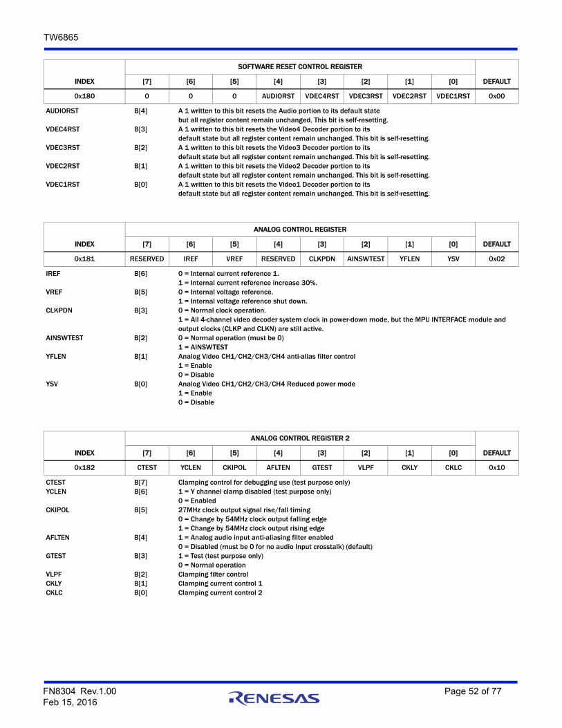
TW6865
INDEX
SOFTWARE RESET CONTROL REGISTER
DEFAULT[7] [6] [5] [4] [3] [2] [1] [0]
0x180 0 0 0 AUDIORST VDEC4RST VDEC3RST VDEC2RST VDEC1RST 0x00
AUDIORST B[4] A 1 written to this bit resets the Audio portion to its default state but all register content remain unchanged. This bit is self-resetting.
VDEC4RST B[3] A 1 written to this bit resets the Video4 Decoder portion to its default state but all register content remain unchanged. This bit is self-resetting.
VDEC3RST B[2] A 1 written to this bit resets the Video3 Decoder portion to itsdefault state but all register content remain unchanged. This bit is self-resetting.
VDEC2RST B[1] A 1 written to this bit resets the Video2 Decoder portion to its default state but all register content remain unchanged. This bit is self-resetting.
VDEC1RST B[0] A 1 written to this bit resets the Video1 Decoder portion to its default state but all register content remain unchanged. This bit is self-resetting.
INDEX
ANALOG CONTROL REGISTER
DEFAULT[7] [6] [5] [4] [3] [2] [1] [0]
0x181 RESERVED IREF VREF RESERVED CLKPDN AINSWTEST YFLEN YSV 0x02
IREF B[6] 0 = Internal current reference 1.1 = Internal current reference increase 30%.
VREF B[5] 0 = Internal voltage reference.1 = Internal voltage reference shut down.
CLKPDN B[3] 0 = Normal clock operation.1 = All 4-channel video decoder system clock in power-down mode, but the MPU INTERFACE module andoutput clocks (CLKP and CLKN) are still active.
AINSWTEST B[2] 0 = Normal operation (must be 0)1 = AINSWTEST
YFLEN B[1] Analog Video CH1/CH2/CH3/CH4 anti-alias filter control1 = Enable0 = Disable
YSV B[0] Analog Video CH1/CH2/CH3/CH4 Reduced power mode1 = Enable0 = Disable
INDEX
ANALOG CONTROL REGISTER 2
DEFAULT[7] [6] [5] [4] [3] [2] [1] [0]
0x182 CTEST YCLEN CKIPOL AFLTEN GTEST VLPF CKLY CKLC 0x10
CTEST B[7] Clamping control for debugging use (test purpose only)YCLEN B[6] 1 = Y channel clamp disabled (test purpose only)
0 = EnabledCKIPOL B[5] 27MHz clock output signal rise/fall timing
0 = Change by 54MHz clock output falling edge1 = Change by 54MHz clock output rising edge
AFLTEN B[4] 1 = Analog audio input anti-aliasing filter enabled0 = Disabled (must be 0 for no audio Input crosstalk) (default)
GTEST B[3] 1 = Test (test purpose only)0 = Normal operation
VLPF B[2] Clamping filter controlCKLY B[1] Clamping current control 1CKLC B[0] Clamping current control 2
FN8304 Rev.1.00 Page 52 of 77Feb 15, 2016

TW6865
INDEX
CONTROL REGISTER I
DEFAULT[7] [6] [5] [4] [3] [2] [1] [0]
0x183 PBW DEM PALSW SET7 COMB HCOMP YCOMB PDLY 0xCC
PBW B[7] 1 = Wide Chroma BPF BW0 = Normal Chroma BPF BW
DEM B[6] ReservedPALSW B[5] 1 = PAL switch sensitivity low.
0 = PAL switch sensitivity normal.SET7 B[4] 1 = The black level is 7.5 IRE above the blank level.
0 = The black level is the same as the blank level.COMB B[3] 1 = Adaptive comb filter for NTSC and PAL (recommended). Not for SECAM.
0 = Notch filter. For SECAMHCOMP B[2] 1 = Adaptive comb filter for NTSC and PAL (recommended). Not for SECAM.
0 = Notch filter. For SECAM.YCOMB B[1] 1 = Bypass Comb filter when no burst presence
0 = No bypassPDLY B[0] PAL delay line.
0 = Enabled1 = Disabled
INDEX
COLOR KILLER HYSTERESIS CONTROL REGISTER
DEFAULT[7] [6] [5] [4] [3] [2] [1] [0]
0x184 GMEN CKHY HSDLY 0x00
GMEN B[7] ReservedCKHY B[6:5] Color killer hysteresis
00b - fastest01b - fast10b - medium11b - slow
HSDLY B[4:0] Reserved for test
INDEX
VERTICAL SHARPNESS
DEFAULT[7] [6] [5] [4] [3] [2] [1] [0]
0x185 SHCOR RESERVED 0x80
SHCOR B[7:4] These bits provide coring function for the sharpness control.
INDEX
CORING CONTROL REGISTER
DEFAULT[7] [6] [5] [4] [3] [2] [1] [0]
0x186 CTCOR CCOR VCOR CIF 0x44
CTCOR B[7:6] These bits control the coring for CTI.CCOR B[5:4] These bits control the low level coring function for the Cb/Cr output. VCOR B[3:2] These bits control the coring function of vertical peaking.CIF B[1:0] These bits control the IF compensation level.
00b = None01b = 1.5dB10b = 3dB11b = 6dB
FN8304 Rev.1.00 Page 53 of 77Feb 15, 2016

TW6865
INDEX
CLAMPING GAIN
DEFAULT[7] [6] [5] [4] [3] [2] [1] [0]
0x187 CLPEND CLPST 0x50
CLPEND B[7:4] These 4 bits set the end time of the clamping pulse. Its valueshould be larger than the value of CLPST.
CLPST B[3:0] These 4 bits set the start time of the clamping. It is referenced to PCLAMP position.
INDEX
INDIVIDUAL AGC GAIN
DEFAULT[7] [6] [5] [4] [3] [2] [1] [0]
0x188 NMGAIN WPGAIN RESERVED 0x22
NMGAIN B[7:4] These bits control the normal AGC loop maximum correction value.WPGAIN B[3:0] Peak AGC loop gain control
INDEX
INDIVIDUAL AGC GAIN
DEFAULT[7] [6] [5] [4] [3] [2] [1] [0]
0x189 RESERVED FC27 VYCOMB VCCOMB WBILINE 0x40
FC27 B[6] 1 = Normal ITU-R656 operation 0 = Squared pixel mode
VYCOMB B[5] Independent VSCALER control VCCOMB B[4] Independent VSCALER controlVVBLINE B[3:0] VBI line enable
INDEX
WHITE PEAK THRESHOLD
DEFAULT[7] [6] [5] [4] [3] [2] [1] [0]
0x18A PEAKWT 0xD8
PEAKWT B[7:0] These bits control the white peak detection threshold. Setting ‘FF’ can disable this function.
INDEX
CLAMP LEVEL
DEFAULT[7] [6] [5] [4] [3] [2] [1] [0]
0x18B CLMPLD CLMPL 0xBC
CLMPLD B[7] 0 = Clamping level is set by CLMPL1 = Clamping level preset at 60d
CLMPL B[6:0] These bits determine the clamping level of the Y channel.
INDEX
SYNC AMPLITUDE
DEFAULT[7] [6] [5] [4] [3] [2] [1] [0]
0x18C SYNCTD SYNCT 0xB8
SYNCTD B[7] 0 = Reference sync amplitude is set by SYNCT1 = Reference sync amplitude is preset to 38h
SYNCT B[6:0] These bits determine the standard sync pulse amplitude for AGC reference.
INDEX
SYNC MISS COUNT REGISTER
DEFAULT[7] [6] [5] [4] [3] [2] [1] [0]
0x18D MISSCNT HSWIN 0x44
MISSCNT B[7:4] These bits set the threshold for horizontal sync miss count threshold.HSWIN B[3:0] These bits determine the VCR mode detection threshold.
FN8304 Rev.1.00 Page 54 of 77Feb 15, 2016

TW6865
INDEX
CLAMP POSITION REGISTER
DEFAULT[7] [6] [5] [4] [3] [2] [1] [0]
0x18E PCLAMP 0x38
PCLAMP B[7:0] These bits set the clamping position from the PLL sync edge
INDEX
VERTICAL CONTROL I
DEFAULT[7] [6] [5] [4] [3] [2] [1] [0]
0x18F VLCK VLCKO VMODE DETV AFLD VINT 0x00
VLCKI B[7:6] Vertical lock in time0 = Fastest3 = Slowest
VLCKO B[5:4] Vertical lock out time0 = Fastest3 = Slowest
VMODE B[3] This bit controls the vertical detection window1 = Search mode0 = Vertical count down mode
DETV B[2] 1 = Recommended for special application only0 = Normal Vsync logic
AFLD B[1] Auto field generation control0 = Off1 = On
VINT B[0] Vertical integration time control1 = Short0 = Normal
INDEX
VERTICAL CONTROL II
DEFAULT[7] [6] [5] [4] [3] [2] [1] [0]
0x190 BSHT VSHT 0x00
BSHT B[7:4] Burst PLL center frequency control.VSHT B[3:0] VSYNC output delay control in the increment of half line length.
INDEX
COLOR KILLER LEVEL CONTROL
DEFAULT[7] [6] [5] [4] [3] [2] [1] [0]
0x191 CKILMAX CKILMIN 0x78
CKILMAX B[7:5] These bits control the amount of color killer hysteresis. The hysteresis amount is proportional to the value.
CKILMIN B[4:0] These bits control the color killer threshold. Larger value gives lower killer level.
INDEX
COMB FILTER CONTROL
DEFAULT[7] [6] [5] [4] [3] [2] [1] [0]
0x192 HTL_MD HTL VTL 0x44
HTL_MD B[7] 0 = Adaptive mode1 = Fixed comb
HTL B[6:4] Adaptive comb filter threshold control 1VTL B[3:0] Adaptive comb filter threshold control 2
FN8304 Rev.1.00 Page 55 of 77Feb 15, 2016
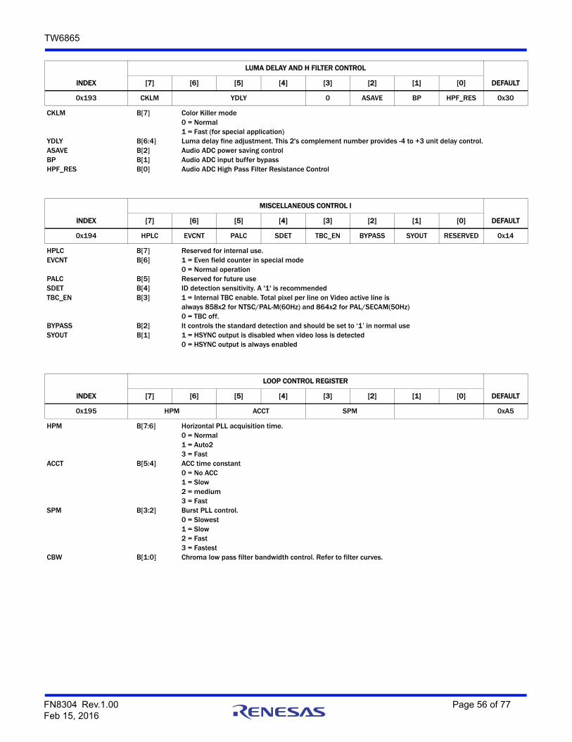
TW6865
INDEX
LUMA DELAY AND H FILTER CONTROL
DEFAULT[7] [6] [5] [4] [3] [2] [1] [0]
0x193 CKLM YDLY 0 ASAVE BP HPF_RES 0x30
CKLM B[7] Color Killer mode 0 = Normal1 = Fast (for special application)
YDLY B[6:4] Luma delay fine adjustment. This 2's complement number provides -4 to +3 unit delay control.ASAVE B[2] Audio ADC power saving controlBP B[1] Audio ADC input buffer bypassHPF_RES B[0] Audio ADC High Pass Filter Resistance Control
INDEX
MISCELLANEOUS CONTROL I
DEFAULT[7] [6] [5] [4] [3] [2] [1] [0]
0x194 HPLC EVCNT PALC SDET TBC_EN BYPASS SYOUT RESERVED 0x14
HPLC B[7] Reserved for internal use.EVCNT B[6] 1 = Even field counter in special mode
0 = Normal operationPALC B[5] Reserved for future useSDET B[4] ID detection sensitivity. A '1' is recommendedTBC_EN B[3] 1 = Internal TBC enable. Total pixel per line on Video active line is
always 858x2 for NTSC/PAL-M(60Hz) and 864x2 for PAL/SECAM(50Hz)0 = TBC off.
BYPASS B[2] It controls the standard detection and should be set to ‘1’ in normal useSYOUT B[1] 1 = HSYNC output is disabled when video loss is detected
0 = HSYNC output is always enabled
INDEX
LOOP CONTROL REGISTER
DEFAULT[7] [6] [5] [4] [3] [2] [1] [0]
0x195 HPM ACCT SPM 0xA5
HPM B[7:6] Horizontal PLL acquisition time.0 = Normal1 = Auto2 3 = Fast
ACCT B[5:4] ACC time constant0 = No ACC1 = Slow2 = medium 3 = Fast
SPM B[3:2] Burst PLL control.0 = Slowest1 = Slow2 = Fast 3 = Fastest
CBW B[1:0] Chroma low pass filter bandwidth control. Refer to filter curves.
FN8304 Rev.1.00 Page 56 of 77Feb 15, 2016

TW6865
INDEX
MISCELLANEOUS CONTROL II
DEFAULT[7] [6] [5] [4] [3] [2] [1] [0]
0x196 NKILL PKILL SKILL CBAL FCS LCS CCS BST 0xE0
NKILL B[7] 1 = Enable noisy signal color killer function in NTSC mode0 = Disabled
PKILL B[6] 1 = Enable automatic noisy color killer function in PAL mode0 = Disabled
SKILL B[5] 1 = Enable automatic noisy color killer function in SECAM mode0 = Disabled
CBAL B[4] 0 = Normal output1 = special output mode
FCS B[3] 1 = Force decoder output value determined by CCS0 = Disabled
LCS B[2] 1 = Enable pre-determined output value indicated by CCS when video loss is detected0 = Disabled.
CCS B[1] When FCS is set high or video loss condition is detected when LCS is set high, one of two colors display can be selected.1 = Blue color.0 = Black.
BST B[0] 1 = Enable blue stretch.0 = Disabled.
INDEX
MISCELLANEOUS CONTROL II
DEFAULT[7] [6] [5] [4] [3] [2] [1] [0]
0x197 FRM YNR CLMD PSP 0x05
FRM B[7:6] Free run mode control0 = Auto2 = Default to 60Hz3 = Default to 50Hz
YNR B[5:4] Y HF noise reduction0 = None1 = Smallest2 = Small3 = Medium
CLMD B[3:2] Clamping mode control0 = Sync top1 = Auto2 = Pedestal3 = N/A
PSP B[1:0 Slice level control0 = Low1 = Medium2 = High
INDEX
HORIZONTAL SCALER PRE-FILTER CONTROL
DEFAULT[7] [6] [5] [4] [3] [2] [1] [0]
0x1A8 HFLT2 HFLT1 0x00
0x1A9 HFLT4 HFLT3 0x00
HFLT Pre-filter selection for Video CH1/CH2/CH3/CH4 horizontal scalerIf HSCALE [11-8] = 1, HFLT [3:0] controls the peaking function.If HSCALE [11-8] > 1, HFLT [2:0] function is below. 1** = Bypass000 = Auto selection based on Horizontal scaling ratio. (default)001 = Recommended for CIF size image010 = Recommended for QCIF size image011 = Recommended for ICON size image
FN8304 Rev.1.00 Page 57 of 77Feb 15, 2016
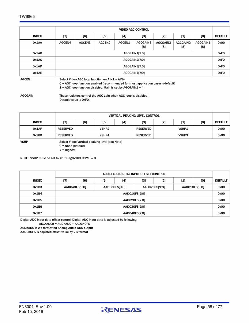
TW6865
INDEX
VIDEO AGC CONTROL
DEFAULT[7] [6] [5] [4] [3] [2] [1] [0]
0x1AA AGCEN4 AGCEN3 AGCEN2 AGCEN1 AGCGAIN4[8]
AGCGAIN3[8]
AGCGAIN2[8]
AGCGAIN1[8]
0x00
0x1AB AGCGAIN1[7:0] 0xF0
0x1AC AGCGAIN2[7:0] 0xF0
0x1AD AGCGAIN3[7:0] 0xF0
0x1AE AGCGAIN4[7:0] 0xF0
AGCEN Select Video AGC loop function on AIN1 ~ AIN4 0 = AGC loop function enabled (recommended for most application cases) (default)1 = AGC loop function disabled. Gain is set by AGCGAIN1 ~ 4
AGCGAIN These registers control the AGC gain when AGC loop is disabled.Default value is 0xF0.
INDEX
VERTICAL PEAKING LEVEL CONTROL
DEFAULT[7] [6] [5] [4] [3] [2] [1] [0]
0x1AF RESERVED VSHP2 RESERVED VSHP1 0x00
0x1B0 RESERVED VSHP4 RESERVED VSHP3 0x00
VSHP Select Video Vertical peaking level (see Note)0 = None (default)7 = Highest
NOTE: VSHP must be set to ‘0’ if Reg0x183 COMB = 0.
INDEX
AUDIO ADC DIGITAL INPUT OFFSET CONTROL
DEFAULT[7] [6] [5] [4] [3] [2] [1] [0]
0x1B3 AADC4OFS[9:8] AADC3OFS[9:8] AADC2OFS[9:8] AADC1OFS[9:8] 0x00
0x1B4 AADC1OFS[7:0] 0x00
0x1B5 AADC2OFS[7:0] 0x00
0x1B6 AADC3OFS[7:0] 0x00
0x1B7 AADC4OFS[7:0] 0x00
Digital ADC input data offset control. Digital ADC input data is adjusted by following: ADJAADCn = AUDnADC + AADCnOFSAUDnADC is 2’s formatted Analog Audio ADC outputAADCnOFS is adjusted offset value by 2’s format
FN8304 Rev.1.00 Page 58 of 77Feb 15, 2016
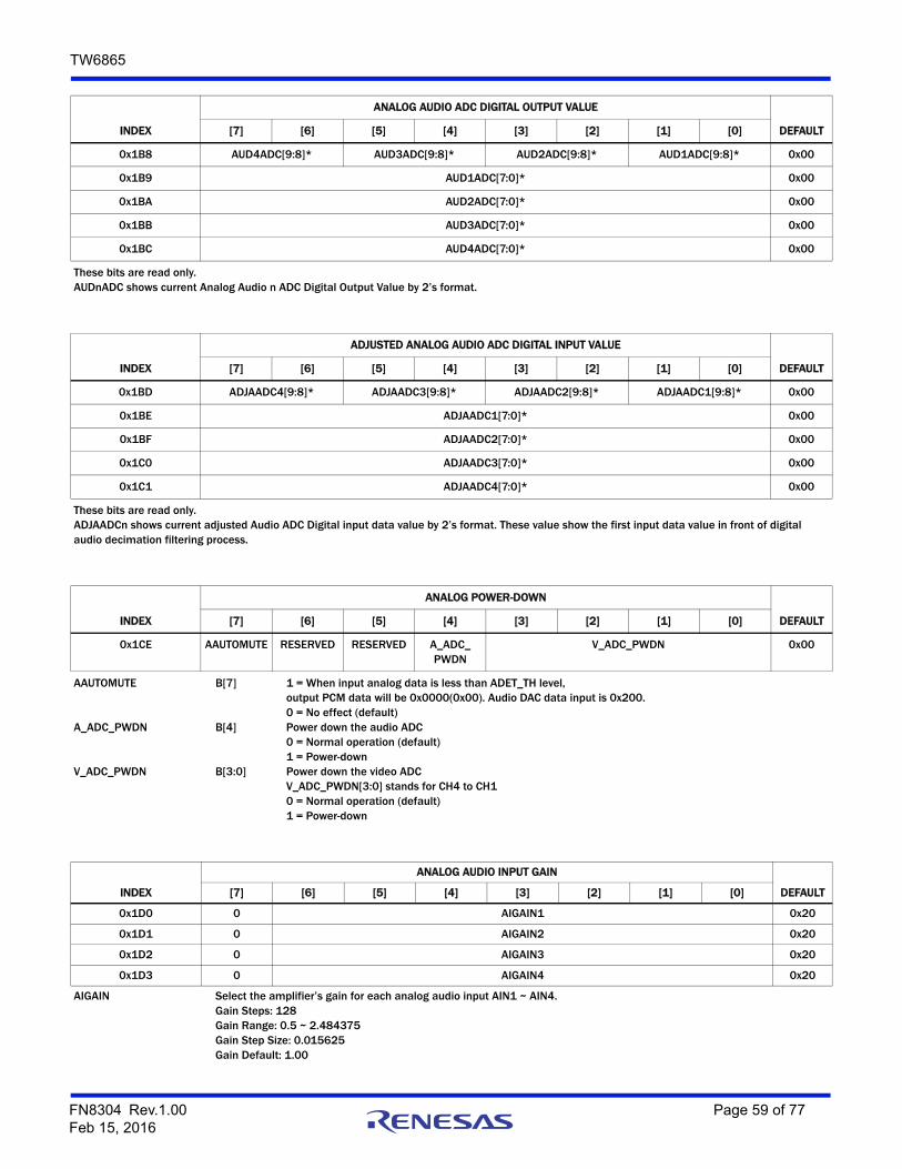
TW6865
INDEX
ANALOG AUDIO ADC DIGITAL OUTPUT VALUE
DEFAULT[7] [6] [5] [4] [3] [2] [1] [0]
0x1B8 AUD4ADC[9:8]* AUD3ADC[9:8]* AUD2ADC[9:8]* AUD1ADC[9:8]* 0x00
0x1B9 AUD1ADC[7:0]* 0x00
0x1BA AUD2ADC[7:0]* 0x00
0x1BB AUD3ADC[7:0]* 0x00
0x1BC AUD4ADC[7:0]* 0x00
These bits are read only.AUDnADC shows current Analog Audio n ADC Digital Output Value by 2’s format.
INDEX
ADJUSTED ANALOG AUDIO ADC DIGITAL INPUT VALUE
DEFAULT[7] [6] [5] [4] [3] [2] [1] [0]
0x1BD ADJAADC4[9:8]* ADJAADC3[9:8]* ADJAADC2[9:8]* ADJAADC1[9:8]* 0x00
0x1BE ADJAADC1[7:0]* 0x00
0x1BF ADJAADC2[7:0]* 0x00
0x1C0 ADJAADC3[7:0]* 0x00
0x1C1 ADJAADC4[7:0]* 0x00
These bits are read only.ADJAADCn shows current adjusted Audio ADC Digital input data value by 2’s format. These value show the first input data value in front of digitalaudio decimation filtering process.
INDEX
ANALOG POWER-DOWN
DEFAULT[7] [6] [5] [4] [3] [2] [1] [0]
0x1CE AAUTOMUTE RESERVED RESERVED A_ADC_PWDN
V_ADC_PWDN 0x00
AAUTOMUTE B[7] 1 = When input analog data is less than ADET_TH level, output PCM data will be 0x0000(0x00). Audio DAC data input is 0x200.0 = No effect (default)
A_ADC_PWDN B[4] Power down the audio ADC0 = Normal operation (default)1 = Power-down
V_ADC_PWDN B[3:0] Power down the video ADCV_ADC_PWDN[3:0] stands for CH4 to CH10 = Normal operation (default)1 = Power-down
INDEX
ANALOG AUDIO INPUT GAIN
DEFAULT[7] [6] [5] [4] [3] [2] [1] [0]
0x1D0 0 AIGAIN1 0x20
0x1D1 0 AIGAIN2 0x20
0x1D2 0 AIGAIN3 0x20
0x1D3 0 AIGAIN4 0x20
AIGAIN Select the amplifier’s gain for each analog audio input AIN1 ~ AIN4. Gain Steps: 128Gain Range: 0.5 ~ 2.484375Gain Step Size: 0.015625Gain Default: 1.00
FN8304 Rev.1.00 Page 59 of 77Feb 15, 2016

TW6865
INDEX
MIX MUTE CONTROL
DEFAULT[7] [6] [5] [4] [3] [2] [1] [0]
0x1DC LAWMD MIX_DERATIO
MIX_MUTE 0x00
LAWMD B[7:6] Select u-Law/A-Law/PCM/SB data output format on ADATR and ADATM pin.0 = PCM output (default)1 = SB (signed MSB bit in PCM data is inverted) output2 = u-Law output3 = A-Law output
MIX_DERATIO B[5] Disable the mixing ratio value for all audio.0 = Apply individual mixing ratio value for each audio (default)1 = Apply nominal value for all audio commonly
MIX_MUTE B[3:0] Enable the mute function for each audio. It effects only for mixing.MIX_MUTE[0]: Audio input AIN1MIX_MUTE[1]: Audio input AIN2MIX_MUTE[2]: Audio input AIN3MIX_MUTE[3]: Audio input AIN4MIX_MUTE[4]: Playback audio inputIt effects only for single chip or the last stage chip0 = Normal (default)1 = Muted
INDEX
MIX RATIO VALUE
DEFAULT[7] [6] [5] [4] [3] [2] [1] [0]
0x1DD MIX_RATIO2 MIX_RATIO1 0x00
0x1DE MIX_RATIO4 MIX_RATIO3 0x00
MIX_RATIO Define the ratio values for audio mixing. MIX_RATIO1: Audio input AIN1MIX_RATIO2: Audio input AIN2MIX_RATIO3: Audio input AIN3MIX_RATIO4: Audio input AIN4It effects only for single chip or the last stage chip.0 0.25 (Recommended for more than 4x AIN1/AIN2/AIN3/AIN4) (default)1 0.312 0.383 0.444 0.505 0.636 0.757 0.888 1.009 1.2510 1.5011 1.7512 2.0013 2.2514 2.5015 2.75
FN8304 Rev.1.00 Page 60 of 77Feb 15, 2016

TW6865
INDEX
MIX OUTPUT SELECTION
DEFAULT[7] [6] [5] [4] [3] [2] [1] [0]
0x1E0 VADCCKPOL
AADCCKPOL
ADACCKPOL
MIX_OUTSEL 0x14
VADCCKPOL B[7] Test purpose only 0 (default)
AADCCKPOL B[6] Test purpose only 0 (default)
ADACCKPOL B[5] Test purpose only 0 (default)
MIX_OUTSEL B[4:0] Define the final audio output for analog and digital mixing out.0 Select record audio of Channel-1 1 Select record audio of Channel-22 Select record audio of Channel-33 Select record audio of Channel-44 Select record audio of Channel-55 Select record audio of Channel-66 Select record audio of Channel-77 Select record audio of Channel-88 Select record audio of Channel-99 Select record audio of Channel-1010 Select record audio of Channel-1111 Select record audio of Channel-1212 Select record audio of Channel-1313 Select record audio of Channel-1414 Select record audio of Channel-1515 Select record audio of Channel-1616 Select playback audio of the first stage chip17 Select playback audio of the second stage chip18 Select playback audio of the third stage chip19 Select playback audio of the last stage chip20 Select mixed audio (default)
INDEX
AUDIO DETECTION PERIOD
DEFAULT[7] [6] [5] [4] [3] [2] [1] [0]
0x1E1 AAMPMD ADET_FILT ADET_TH4[4] ADET_TH3[4] ADET_TH2[4] ADET_TH1[4] 0xC0
AAMPMD B[7] Define the audio detection method.0 = Detect audio if absolute amplitude is greater than threshold (default)1 = Detect audio if differential amplitude is greater than threshold
ADET_FILT B[6:5] Select the filter for audio detection0 = Wide LPF (default)…..7 = Narrow LPF
FN8304 Rev.1.00 Page 61 of 77Feb 15, 2016

TW6865
INDEX
AUDIO DETECTION THRESHOLD
DEFAULT[7] [6] [5] [4] [3] [2] [1] [0]
0x1E1 AAMPMD ADET_FILT ADET_TH4[4] ADET_TH3[4] ADET_TH2[4] ADET_TH1[4] 0xC0
0x1E2 ADET_TH2[3:0] ADET_TH1[3:0] 0xAA
0x1E3 ADET_TH4[3:0] ADET_TH3[3:0] 0xAA
ADET_TH Define the threshold value for audio detection.ADET_TH1: Audio input AIN1ADET_TH2: Audio input AIN2ADET_TH3: Audio input AIN3ADET_TH4: Audio input AIN40 Low value (default)31 High value
If fs = 8kHz Audio Clock setting mode:Reg0x1E1 = 0xC0, Reg0x1E2 = 0xAA, Reg0x1E3 = 0xAA are typical setting value.If fs = 16kHz/32kHz/44.1kHz/48kHz Audio Clock setting mode:Reg0x1E1=0xE0, Reg0x1E2 = 0xBB, Reg0x1E3 = 0xBB are typical setting value.
INDEX
AADC_TEST
DEFAULT[7] [6] [5] [4] [3] [2] [1] [0]
0x1FC 0 ASYNSERIAL AADC_PFTEST
AINSWFIX AINSWNUM 0x00
Audio ADC test controls These bits are not for normal usage.
INDEX
VADC_TEST
DEFAULT[7] [6] [5] [4] [3] [2] [1] [0]
0x1FD 0 0 0 0 0 VADC_PFTEST
VADC_PFSEL 0x00
Video ADC test controls These bits are not for normal usage.
INDEX
DEVICE ID
DEFAULT[7] [6] [5] [4] [3] [2] [1] [0]
0x1FE DEV_ID[5:4]*: 0h 0 0 0 0 0 0 0x00
0x1FF DEV_ID[3:0]*: 7h 0 0 0 1 0x71
DEV_ID Device ID (0x07)
FN8304 Rev.1.00 Page 62 of 77Feb 15, 2016
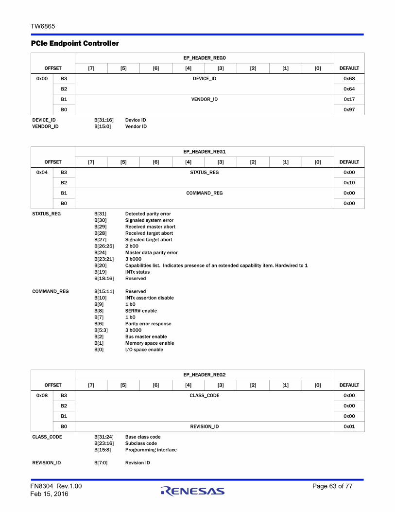
TW6865
PCIe Endpoint Controller
OFFSET
EP_HEADER_REG0
DEFAULT[7] [5] [6] [4] [3] [2] [1] [0]
0x00 B3 DEVICE_ID 0x68
B2 0x64
B1 VENDOR_ID 0x17
B0 0x97
DEVICE_ID B[31:16] Device IDVENDOR_ID B[15:0] Vendor ID
OFFSET
EP_HEADER_REG1
DEFAULT[7] [5] [6] [4] [3] [2] [1] [0]
0x04 B3 STATUS_REG 0x00
B2 0x10
B1 COMMAND_REG 0x00
B0 0x00
STATUS_REG B[31] Detected parity errorB[30] Signaled system errorB[29] Received master abortB[28] Received target abortB[27] Signaled target abortB[26:25] 2’b00B[24] Master data parity errorB[23:21] 3’b000B[20] Capabilities list. Indicates presence of an extended capability item. Hardwired to 1B[19] INTx statusB[18:16] Reserved
COMMAND_REG B[15:11] ReservedB[10] INTx assertion disableB[9] 1’b0B[8] SERR# enableB[7] 1’b0B[6] Parity error responseB[5:3] 3’b000B[2] Bus master enableB[1] Memory space enableB[0] I/O space enable
OFFSET
EP_HEADER_REG2
DEFAULT[7] [5] [6] [4] [3] [2] [1] [0]
0x08 B3 CLASS_CODE 0x00
B2 0x00
B1 0x00
B0 REVISION_ID 0x01
CLASS_CODE B[31:24] Base class codeB[23:16] Subclass codeB[15:8] Programming interface
REVISION_ID B[7:0] Revision ID
FN8304 Rev.1.00 Page 63 of 77Feb 15, 2016

TW6865
OFFSET
EP_HEADER_REG3
DEFAULT[7] [5] [6] [4] [3] [2] [1] [0]
0x0C B3 BIST 0x00
B2 HEADER_TYPE 0x00
B1 LATENCY_TIMER 0x00
B0 CACHE_LINE_SIZE 0x00
BIST B[31:24] 8’h00
HEADER_TYPE B[23] 1’b0B[22:16] Configuration header format (hardwired to 0 for type 0.)
LATENCY_TIMER B[15:8] 8’h00
CACHE_LINE_SIZE B[7:0] 8’h00
OFFSET
EP_HEADER_REG4 ~ EP_HEADER_REG9
DEFAULT[7] [5] [6] [4] [3] [2] [1] [0]
0x10 B3 BASE_ADDRESS_REG0 0x00
B2 0x00
B1 0x00
B0 0x08
0x14 B3 BASE_ADDRESS_REG1 0x00
B2 0x00
B1 0x00
B0 0x00
0x18 B3 BASE_ADDRESS_REG2 0x00
B2 0x00
B1 0x00
B0 0x00
0x1C B3 BASE_ADDRESS_REG3 0x00
B2 0x00
B1 0x00
B0 0x00
0x20 B3 BASE_ADDRESS_REG4 0x00
B2 0x00
B1 0x00
B0 0x00
0x24 B3 BASE_ADDRESS_REG5 0x00
B2 0x00
B1 0x00
B0 0x00
BASE_ADDRESS B[31:4] BAR base address bitsB[3] If BAR is a memory BAR, bit 3 indicates if the memory region is prefetchable:
0 = Non-prefetchable1 = PrefetchableIf BAR is an I/O BAR, bit 3 is the second least significant bit of the base address.
B[2:1] 2’b00B[0] 0 = BAR is a memory BAR
1 = BAR is an I/O BAR
FN8304 Rev.1.00 Page 64 of 77Feb 15, 2016

TW6865
OFFSET
EP_HEADER_REGA
DEFAULT[7] [5] [6] [4] [3] [2] [1] [0]
0x28 B3 CARDBUS_CIS_POINTER 0x00
B2 0x00
B1 0x00
B0 0x00
CARDBUS_CIS_POINTER B[31:0] CardBus CIS pointer
OFFSET
EP_HEADER_REGB
DEFAULT[7] [5] [6] [4] [3] [2] [1] [0]
0x2C B3 SUBSYSYEM_ID 0x00
B2 0x00
B1 SUBSYSYEM_VENDOR_ID 0x00
B0 0x00
SUBSYSYEM_ID B[31:16] Subsystem IDSUBSYSYEM_VENDOR_ID B[15:0] Subsystem Vendor ID
OFFSET
EP_HEADER_REGC
DEFAULT[7] [5] [6] [4] [3] [2] [1] [0]
0x30 B3 EXPANSION_ROM_BASE_ADDR 0x00
B2 0x00
B1 0x00
B0 0x00
EXPANSION_ROM_BASE_ADDRB[31:11] Expansion ROM AddressB[10:1] ReservedB[0] Expansion ROM Enable
OFFSET
EP_HEADER_REGD
DEFAULT[7] [5] [6] [4] [3] [2] [1] [0]
0x34 B3 0x00
B2 0x00
B1 0x00
B0 CAP_PTR 0x40
CAP_PTR B[7:0] First capability pointer. Points to power management capability structure by default.
FN8304 Rev.1.00 Page 65 of 77Feb 15, 2016
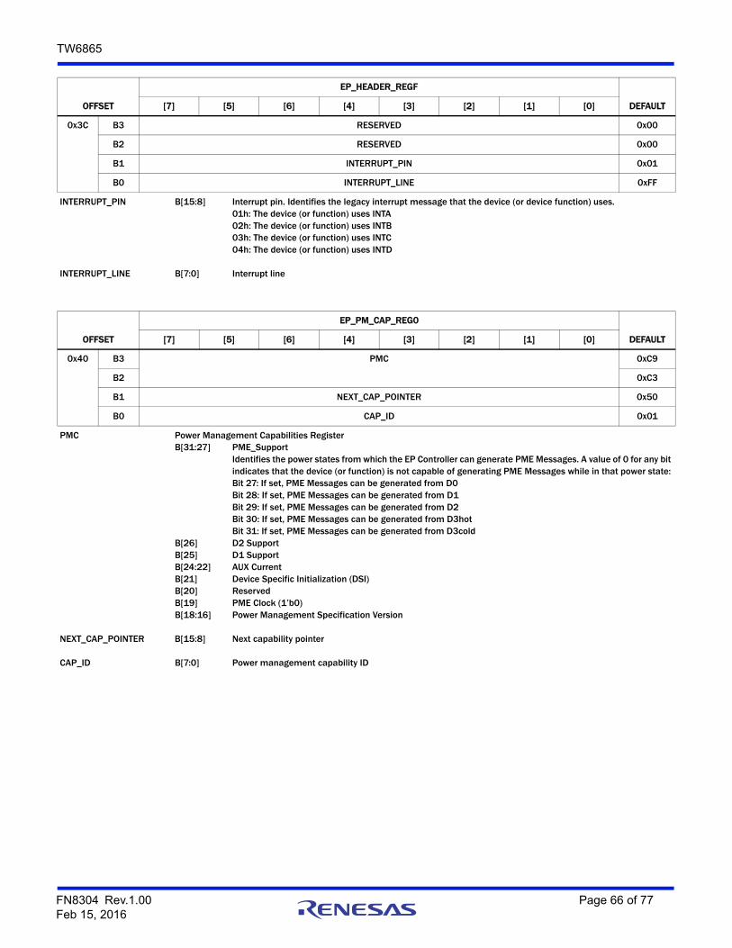
TW6865
OFFSET
EP_HEADER_REGF
DEFAULT[7] [5] [6] [4] [3] [2] [1] [0]
0x3C B3 RESERVED 0x00
B2 RESERVED 0x00
B1 INTERRUPT_PIN 0x01
B0 INTERRUPT_LINE 0xFF
INTERRUPT_PIN B[15:8] Interrupt pin. Identifies the legacy interrupt message that the device (or device function) uses. 01h: The device (or function) uses INTA02h: The device (or function) uses INTB03h: The device (or function) uses INTC04h: The device (or function) uses INTD
INTERRUPT_LINE B[7:0] Interrupt line
OFFSET
EP_PM_CAP_REG0
DEFAULT[7] [5] [6] [4] [3] [2] [1] [0]
0x40 B3 PMC 0xC9
B2 0xC3
B1 NEXT_CAP_POINTER 0x50
B0 CAP_ID 0x01
PMC Power Management Capabilities RegisterB[31:27] PME_Support
Identifies the power states from which the EP Controller can generate PME Messages. A value of 0 for any bit indicates that the device (or function) is not capable of generating PME Messages while in that power state:Bit 27: If set, PME Messages can be generated from D0Bit 28: If set, PME Messages can be generated from D1Bit 29: If set, PME Messages can be generated from D2Bit 30: If set, PME Messages can be generated from D3hotBit 31: If set, PME Messages can be generated from D3cold
B[26] D2 SupportB[25] D1 SupportB[24:22] AUX CurrentB[21] Device Specific Initialization (DSI)B[20] ReservedB[19] PME Clock (1’b0)B[18:16] Power Management Specification Version
NEXT_CAP_POINTER B[15:8] Next capability pointer
CAP_ID B[7:0] Power management capability ID
FN8304 Rev.1.00 Page 66 of 77Feb 15, 2016

TW6865
OFFSET
EP_PM_CAP_REG1
DEFAULT[7] [5] [6] [4] [3] [2] [1] [0]
0x44 B3 DATA 0x00
B2 PMCSR_BSE_EXT 0x00
B1 PMCSR 0x00
B0 0x00
DATA B[31:24] 8’h00
PMCSR_BSE_EXT B[23] Bus power/clock control enable (hardwired to 0)B[22] B2/B3 support (hardwired to 0)B[21:16] Reserved
PMCSR B[15] PME statusB[14:13] Data scale (not supported)B[12:9] Data select (not supported)B[8] PME enable. A value of 1 indicates that the device is enabled to generate PMEB[7:4] ReservedB[3] No soft resetB[2] ReservedB[1:0] Power state
Controls the device power state:00b: D001b: D110b: D211b: D3
OFFSET
EP_PCIE_CAP_REG0
DEFAULT[7] [5] [6] [4] [3] [2] [1] [0]
0x70 B3 PCIE_CAP_REG 0x00
B2 0x12
B1 NEXT_CAP_POINTER 0x00
B0 CAP_ID 0x10
PCIE_CAP_REG B[31:30] ReservedB[29:25] Interrupt message numberB[24] Slot implemented (it must 0 for an EP device)B[23:20] Device port typeB[19:16] PCI Express capability version
NEXT_CAP_POINTER B[15:8] Next capability pointer
CAP_ID B[7:0] PCI Express capability ID
FN8304 Rev.1.00 Page 67 of 77Feb 15, 2016

TW6865
OFFSET
EP_PCIE_CAP_REG1
DEFAULT[7] [5] [6] [4] [3] [2] [1] [0]
0x74 B3 DEVICE_CAP 0x00
B2 0x00
B1 0x87
B0 0x22
DEVICE_CAP B[31:28] ReservedB[27:26] Captured slot power limit scale. From message from RC, upstream port only.B[25:18] Captured slot power limit value. From message from RC, upstream port only.B[17:16] ReservedB[15] Role-based error reportingB[14:12] 3’b000B[11:9] Endpoint L1 acceptable latencyB[8:6] Endpoint L0s acceptable latencyB[5] Extended tag field supportedB[4:3] Phantom function supported (must be 0)B[2:0] Max_Payload_Size supported
OFFSET
EP_PCIE_CAP_REG2
DEFAULT[7] [5] [6] [4] [3] [2] [1] [0]
0x78 B3 DEVICE_STATUS 0x00
B2 0x10
B1 DEVICE_CONTROL 0x20
B0 0x10
DEVICE_STATUS B[31:22] ReservedB[21] Transaction pending
Set to 1 when non-posted requests are not yet completed and clear when they are completed.B[20] Aux power detected
Set to 1 if Aux power detectedB[19] Unsupported request detected
Errors are logged in this register regardless of whether error reporting is enabled in the device control register.B[18] Fatal error detected
Errors are logged in this register regardless of whether error reporting is enabled in the device control register.B[17] Non-fatal error detected
Errors are logged in this register regardless of whether error reporting is enabled in the device control register.B[16] Correctable error detected
Errors are logged in this register regardless of whether error reporting is enabled in the device control register.
DEVICE_CONTROL B[15] ReservedB[14:12] Max_Read_Request_SizeB[11] Enable no snoopB[10] AUX power PM enableB[9] Phantom function enableB[8] Extended tag field enableB[7:5] Max_Payload_SizeB[4] Enable relaxed orderingB[3] Unsupported request reporting enableB[2] Fatal error reporting enableB[1] Non-Fatal error reporting enableB[0] Correctable error reporting enable
FN8304 Rev.1.00 Page 68 of 77Feb 15, 2016

TW6865
OFFSET
EP_PCIE_CAP_REG3
DEFAULT[7] [5] [6] [4] [3] [2] [1] [0]
0x7C B3 LINK_CAP 0x00
B2 0x07
B1 0x3C
B0 0x11
LINK_CAP B[31:24] Port numberB[23:22] ReservedB[21] Link bandwidth notification capability
Set to 1 for endpoint devicesB[20] Data link layer active reporting capable
Set to 1 for endpoint devicesB[19] Surprise down error reporting capable
Not supported, hardwired to 0x0B[18] Clock power managementB[17:15] L1 exit latencyB[14:12] L0s exit latencyB[11:10] Active state link PM supportB[9:4] Maximum link widthB[3:0] Maximum link speed
OFFSET
EP_PCIE_CAP_REG4
DEFAULT[7] [5] [6] [4] [3] [2] [1] [0]
0x80 B3 LINK_STATUS 0x10
B2 0x11
B1 LINK_CONTROL 0x00
B0 0x00
LINK_STATUS B[31] Link autonomous bandwidth statusB[30] Link bandwidth management statusB[29] Data link layer active (hardwired to 0)B[28] Slot clock configurationB[27] Link training (hardwired to 0)B[26] ReservedB[25:20] Negotiated link width
Set automatically by hardware after link initialization.B[19:16] Link speed
The negotiated link speed: 2.5 Gbps
LINK_CONTROL B[15:12] ReservedB[11] Link autonomous bandwidth interrupt enable (reserved for endpoints)B[10] Link bandwidth management interrupt enable (reserved for endpoints)B[9] Hardware autonomous width disable (not supported)B[8] Enable clock power management
Hardwired to 0 if Clock power management Jis disabled in the Link capabilities register.
B[7] Extended synchB[6] Common clock configurationB[5] Retrain link (hardwired to 0)B[4] Link disable (hardwired to 0)B[3] Read completion boundary (RCB)B[2] ReservedB[1:0] Active state link PM control
FN8304 Rev.1.00 Page 69 of 77Feb 15, 2016

TW6865
OFFSET
EP_ERR_CAP_REG0
DEFAULT[7] [5] [6] [4] [3] [2] [1] [0]
0x100 B3 ENHANCE_CAP_HEADER 0x14
B2 0x01
B1 0x00
B0 0x01
ENHANCE_CAP_HEADERB[31:20] Next capability offsetB[19:16] Capability versionB[15:0] PCI Express extended capability ID
Default value is 0x1 for advanced error reporting
OFFSET
EP_ERR_CAP_REG1
DEFAULT[7] [5] [6] [4] [3] [2] [1] [0]
0x104 B3 UNCORRECTABLE_ERROR_STATUS 0x00
B2 0x00
B1 0x00
B0 0x00
UNCORRECTABLE_ERROR_STATUSB[31:21] ReservedB[20] Unsupported request error statusB[19] ECRC error statusB[18] Malformed TLP statusB[17] Receiver overflow statusB[16] Unexpected completion statusB[15] Completer abort statusB[14] Completion timeout statusB[13] Flow control protocol error statusB[12] Poisoned TLP statusB[11:6] ReservedB[5] Surprise down error status (not supported)B[4] Data link protocol error statusB[3:0] Reserved
FN8304 Rev.1.00 Page 70 of 77Feb 15, 2016

TW6865
OFFSET
EP_ERR_CAP_REG2
DEFAULT[7] [5] [6] [4] [3] [2] [1] [0]
0x108 B3 UNCORRECTABLE_ERROR_MASK 0x00
B2 0x00
B1 0x00
B0 0x00
UNCORRECTABLE_ERROR_MASKB[31:21] ReservedB[20] Unsupported request error maskB[19] ECRC error maskB[18] Malformed TLP maskB[17] Receiver overflow maskB[16] Unexpected completion maskB[15] Completer abort maskB[14] Completion timeout maskB[13] Flow control protocol error maskB[12] Poisoned TLP maskB[11:6] ReservedB[5] Surprise down error mask (not supported)B[4] Data link protocol error maskB[3:0] Reserved
OFFSET
EP_ERR_CAP_REG3
DEFAULT[7] [5] [6] [4] [3] [2] [1] [0]
0x10C B3 UNCORRECTABLE_ERROR_SEVERITY 0x00
B2 0x06
B1 0x20
B0 0x30
UNCORRECTABLE_ERROR_SEVERITYB[31:21] ReservedB[20] Unsupported request error severityB[19] ECRC error severityB[18] Malformed TLP severityB[17] Receiver overflow severityB[16] Unexpected completion severityB[15] Completer abort severityB[14] Completion timeout severityB[13] Flow control protocol error severityB[12] Poisoned TLP severityB[11:6] ReservedB[5] Surprise down error severity (not supported)B[4] Data link protocol error severityB[3:0] Reserved
FN8304 Rev.1.00 Page 71 of 77Feb 15, 2016
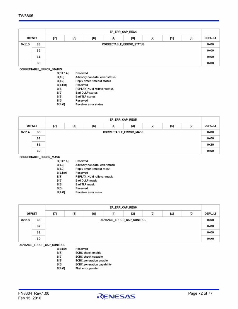
TW6865
OFFSET
EP_ERR_CAP_REG4
DEFAULT[7] [5] [6] [4] [3] [2] [1] [0]
0x110 B3 CORRECTABLE_ERROR_STATUS 0x00
B2 0x00
B1 0x00
B0 0x00
CORRECTABLE_ERROR_STATUSB[31:14] ReservedB[13] Advisory non-fatal error statusB[12] Reply timer timeout statusB[11:9] ReservedB[8] REPLAY_NUM rollover statusB[7] Bad DLLP statusB[6] Bad TLP statusB[5] ReservedB[4:0] Receiver error status
OFFSET
EP_ERR_CAP_REG5
DEFAULT[7] [5] [6] [4] [3] [2] [1] [0]
0x114 B3 CORRECTABLE_ERROR_MASK 0x00
B2 0x00
B1 0x20
B0 0x00
CORRECTABLE_ERROR_MASKB[31:14] ReservedB[13] Advisory non-fatal error maskB[12] Reply timer timeout maskB[11:9] ReservedB[8] REPLAY_NUM rollover maskB[7] Bad DLLP maskB[6] Bad TLP maskB[5] ReservedB[4:0] Receiver error mask
OFFSET
EP_ERR_CAP_REG6
DEFAULT[7] [5] [6] [4] [3] [2] [1] [0]
0x118 B3 ADVANCE_ERROR_CAP_CONTROL 0x00
B2 0x00
B1 0x00
B0 0xA0
ADVANCE_ERROR_CAP_CONTROLB[31:9] ReservedB[8] ECRC check enableB[7] ECRC check capableB[6] ECRC generation enableB[5] ECRC generation capabilityB[4:0] First error pointer
FN8304 Rev.1.00 Page 72 of 77Feb 15, 2016

TW6865
OFFSET
EP_ERR_CAP_REG7~ EP_ERR_CAP_REGA
DEFAULT[7] [5] [6] [4] [3] [2] [1] [0]
0x11C B3 HEADER_LOG_1ST_DW 0x00
B2 0x00
B1 0x00
B0 0x00
0x120 B3 HEADER_LOG_2RD_DW 0x00
B2 0x00
B1 0x00
B0 0x00
0x124 B3 HEADER_LOG_3RD_DW 0x00
B2 0x00
B1 0x00
B0 0x00
0x128 B3 HEADER_LOG_4TH_DW 0x00
B2 0x00
B1 0x00
B0 0x00
These 4 header registers collect the header for the TLP corresponding to a detected error.
FN8304 Rev.1.00 Page 73 of 77Feb 15, 2016

TW6865
Audio Decimation Filter Response
FIGURE 10. AUDIO DECIMATION FILTER: (*) 0.016 LINE = 0.016x64xFS
0
-5
-10
-15
-20
-25
-30
-35
-40
0 0.002 0.004 0.006 0.008 0.010 0.012 0.014 0.016
FREQUENCY (NORMALIZED TO 64 x FS)
GA
IN (
dB
)
-45
-50
FN8304 Rev.1.00 Page 74 of 77Feb 15, 2016
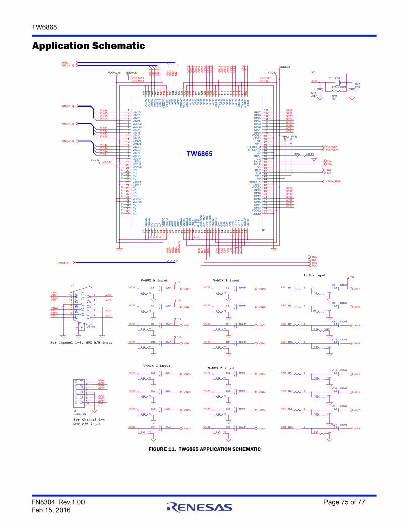
TW6865
Application Schematic
AIN[8..5]
AIN
7A
IN6
AIN
8
AIN
5A
IN1
AIN
2
VDD12VDD12
VDDE33
VDDE33
VDD12
GP
4
GP
9G
P8
GP
7G
P6
GP
5
GP
12G
P11
VIN1[4..1]
VIN2[4..1]
VIN3[4..1]
VIN4[4..1]
GP
10
GP17GP16GP15GP14GP13
VDD12
GP22GP21GP20
GP19GP18
GP27GP26GP25GP24GP23
GP
33G
P32
GP
31G
P30
GP
29G
P28
GP
38G
P37
GP
36G
P35
GP
34
GP
42G
P41
GP
40G
P39
AIN[4..1]
TW6865
U1
VDDV820 VDD1219 VSS1218 VDDV417
VIN4B15
VIN4A16
VIN4C14
VSSV412
VIN4D13
VSSV311
GP
664
GP
765
VIN3A7 VDDV36 VDDV25 VIN2A4 VIN2B3
VD
D33
71
VS
S3
372
VSS1273VDD1274GP1375GP1476GP1577GP1678GP1779GP1880GP1981VDD3382VSS3383PERST_N84VP85VPH86TX_M87TX_P88GD89RX_P90RX_M91GD92REXT93GD94REFCLK_P95REFCLK_M96VPH97VP98VSS3399VDD33100GP20101
GP22103GP23104
GP21102
GP24105GP25106GP26107GP27108
XT
ALI
109
XT
ALO
110
VD
D12
111
VS
S12
112
GP
2811
3G
P29
114
GP
3011
5G
P31
116
GP
3211
7G
P33
118
VD
D33
119
VS
S33
120
GP
3412
1G
P35
122
GP
3612
3G
P37
124
GP
3812
5G
P39
126
GP
4012
7G
P41
128
GP
4212
9V
SS
1213
0V
DD
1213
1V
DD
A1
132
AIN
113
3A
IN2
134
AIN
313
5A
IN4
136
VS
SA
113
7V
DD
V1
138
VIN
1A
139
VIN
1B
140
VIN
1C14
1V
IN1D
142
VS
SV
114
3V
SS
V2
144
GP
1270
VIN2D1
VIN2C2
GP
1169
GP
1068
GP
967
GP
866
VIN3C9
VIN3D10
GP
563
GP
462
GP
3/T
DO
59G
P2/
TD
I58
GP
1/T
MS
57G
P0/
TC
K56
R_S
EL
55T
ES
T1
53T
ES
T0
52V
DD
3351
VS
S3
350
VD
DA
249
VSSV825
VSSV726
AIN
746
AIN
845
VS
SA
244
VD
DV
543
NC
42N
C41
NC
40N
C39
VS
SV
637
VS
SV
538
VD
D12
61V
SS
12
60
VIN3B8
T_S
EL
54
NC21
NC22
NC23
NC24
AIN
548
AIN
647
NC28 NC27
NC29
NC30
VDDV731
VDDV632
NC33
NC34
NC35
NC36
VDDAV33
XT
OX
TI
XTI
REFCLK+REFCLK-
R50 190 1%
VDDAV33
AIN
4A
IN3
VIN
14V
IN13
VIN
12V
IN11
TXpTXn
RXpRXn
/PCIe_RST
VP12 VP33
VDDAA33
XTOVDDAA33
VIN22VIN21
VIN24VIN23
VIN34VIN33VIN32VIN31
VIN44
VIN41VIN42VIN43
VD
DA
A33
TDO
TCKTMSTDI
C4222pF
C4122pF
Y1 27Mhz
XTAL\HC49
TM
ST
CK
TD
IT
DO
R491M
AID3
AID4
R15 75
R28 10K
TP4
R2 75
R14 75
R17 0
TP9
C1 100nF
R20 10K
C910uF
C1206
C10 100nF
TP3
R5 0
R6 75
R4 10K
C1210uF
C1206
C1810uF
C1206
R11 75
R21 0
R16 10K
C310uF
C1206
C4 100nF
R32 10K
TP1
C8 100nF
C2110uF
C1206
R9 0
R8 10K
R10 75
R1 0
TP2
R7 75
R24 10K
R25 0
C2410uF
C1206
C7 100nF
C610uF
C1206C5 100nF
J1
DB-15B
11
22
33
44
5510
10
99
88
77
66
1111
1212
1313
1414
1515
G1
6
G1
7
R13 0
C1510uF
C1206
R3 75
C11 100nF
R12 10K
C2 100nF
R29 0
VIN21
VIN11
VIN41
VIN31
VIN22
VIN12 AIN1
VIN42
VIN32
AIN4
AIN3
AIN2
AIN7
AIN6
AIN5
AIN8
JP1Header 5X2
12345678910
VID23VID24
VID33VID34VID43VID44
For Channel 1~4MUX C/D input
VID13VID14
R37 75
C29 100nF
R39 75
C31 100nF
R33 75
C25 100nF
R35 75
C27 100nF VIN23
VIN13
VIN43
VIN33VID33
VID43
VID13
VID23
For Channel 1~4, MUX A/B input
R34 75
V-MUX A input
C28 100nF
C26 100nF
V-MUX B input
R40 75
C32 100nF
C30 100nF
R38 75
R36 75
VIN34
VIN24
VIN14
VIN44
VID24
VID14
VID44
VID34
Audio input
V-MUX D inputV-MUX C input
AID1
VID42
AID2
AID3
AID4
AID5
AID6
AID7
AID8
VID32
VID11
VID22
VID12
VID31
VID21
VID41
VID42
VID31
VID21VID12
VID22
VID32
AID1
AID2
VID41
VID11
FIGURE 11. TW6865 APPLICATION SCHEMATIC
FN8304 Rev.1.00 Page 75 of 77Feb 15, 2016
TW6865
Intersil products are manufactured, assembled and tested utilizing ISO9001 quality systems as notedin the quality certifications found at www.intersil.com/en/support/qualandreliability.html
Intersil products are sold by description only. Intersil may modify the circuit design and/or specifications of products at any time without notice, provided that such modification does not, in Intersil's sole judgment, affect the form, fit or function of the product. Accordingly, the reader is cautioned to verify that datasheets are current before placing orders. Information furnished by Intersil is believed to be accurate and reliable. However, no responsibility is assumed by Intersil or its subsidiaries for its use; nor for any infringements of patents or other rights of third parties which may result from its use. No license is granted by implication or otherwise under any patent or patent rights of Intersil or its subsidiaries.
For information regarding Intersil Corporation and its products, see www.intersil.com
For additional products, see www.intersil.com/en/products.html
© Copyright Intersil Americas LLC 2012-2016. All Rights Reserved.All trademarks and registered trademarks are the property of their respective owners.
About IntersilIntersil Corporation is a leading provider of innovative power management and precision analog solutions. The company's products address some of the largest markets within the industrial and infrastructure, mobile computing and high-end consumer markets.
For the most updated datasheet, application notes, related documentation and related parts, please see the respective product information page found at www.intersil.com.
You may report errors or suggestions for improving this datasheet by visiting www.intersil.com/ask.
Reliability reports are also available from our website at www.intersil.com/support.
Revision HistoryThe revision history provided is for informational purposes only and is believed to be accurate, but not warranted. Please go to the web to make sure that you have the latest revision.
DATE REVISION CHANGE
February 15, 2016 FN8304.1 Updated datasheet to Intersil standard Frame format.Added About Intersil verbiage.Updated “Ordering Information” on page 6 by adding “H” part.
April 12, 2012 FN8304.0 Initial release.
FN8304 Rev.1.00 Page 76 of 77Feb 15, 2016

TW6865
FN8304 Rev.1.00 Page 77 of 77Feb 15, 2016
Package Outline DrawingQ144.20x20C144 LEAD THIN QUAD FLATPACK PACKAGE (TQFP)
Rev 0, 2/12
SIDE VIEW
TOP VIEW
SYMBOL
MILLIMETERS MILLIMETERS
MIN NOM MAX MIN NOM MAX
A 1.00 1.10 1.20 0.039 0.043 0.047
A1 0.05 0.10 0.15 0.002 0.004 0.006
A2 0.95 1.00 1.05 0.037 0.039 0.041
D 22.00 BSC 0.866 BSC
D1 20.00 BSC 0.787 BSC
E 22.00 BSC 0.866 BSC
E1 20.00 BSC 0.787 BSC
R2 0.08 - 0.20 0.003 - 0.008
R1 0.08 - - 0.003 - -
0° 3.5° 7° 0° 3.5° 7°
1 0° - - 0° - -
2 11° 12° 13° 11° 12° 13°
3 11° 12° 13° 11° 12° 13°
c 0.09 - 0.20 0.004 - 0.008
L 0.45 0.60 0.75 0.018 0.024 0.030
L1 1.00 REF 0.039 REF
S 0.20 - - 0.008 - -
SYMBOL
144L
MILLIMETERS MILLIMETERS
MIN NOM MAX MIN NOM MAX
b 0.17 0.20 0.27 0.007 0.008 0.011
e 0.50 BSC 0.020 BSC
D2 17.50 0.689
E2 17.50 0.689
TOLERANCES OF FORM AND POSITION
aaa 0.20 0.008
bbb 0.20 0.008
ccc 0.08 0.003
ddd 0.08 0.003
NOTES:
1. Dimensions D1 and E1 do not include mold protrusion. Allowable protrusion is 0.25mm per side. D1 and E1 are maximum plastic body size dimensions including mold mismatch.
2. Dimension b does not include dambar protrusion. Allowable dambar protrusion shall not cause the lead width to exceed the maximum b dimension by more than 0.08mm. Dambar cannot be located on the lower radius or the foot. Minimum space between protrusion and an adjacent lead is 0.07mm for 0.4mm and 0.5mm pitch packages.
3. Control dimensions are in millimeters.
DETAIL "X"
SEE DETAIL "X"
D
D1
D2
-D-
E2
E1E
-A-
e b
4X
4X
-B-
L1
A2
A
A1
ccc C -C- SEATING PLANE
1
S3
R2R1
0.25mm
GAUGE
2
-H-
L
C
aaa C A-B D
bbb H A-B D
ddd M C A-B s D s
PLANE
0.0
5 S
-