datasheet - renesas.com · pclk 2 o peripheral clock: pclk is a peripheral clock signal whose...
TRANSCRIPT

FN2974Rev 4.00
Sep 9, 2015
82C84ACMOS Clock Generator Driver
DATASHEET
The Intersil 82C84A is a high performance CMOS Clock Generator-driver which is designed to service the requirements of both CMOS and NMOS microprocessors such as the 80C86, 80C88, 8086 and the 8088. The chip contains a crystal controlled oscillator, a divide-by-three counter and complete “Ready” synchronization and reset logic.
Static CMOS circuit design permits operation with an external frequency source from DC to 25MHz. Crystal controlled operation to 25MHz is guaranteed with the use of a parallel, fundamental mode crystal and two small load capacitors.
All inputs (except X1 and RES) are TTL compatible over temperature and voltage ranges.
Power consumption is a fraction of that of the equivalent bipolar circuits. This speed-power characteristic of CMOS permits the designer to custom tailor his system design with respect to power and/or speed requirements.
Features
• Generates the System Clock For CMOS or NMOS Microprocessors
• Up to 25MHz Operation
• Uses a Parallel Mode Crystal Circuit or ExternalFrequency Source
• Provides Ready Synchronization
• Generates System Reset Output From Schmitt Trigger Input
• TTL Compatible Inputs/Outputs
• Very Low Power Consumption
• Single 5V Power Supply
• Operating Temperature Ranges
- C82C84A . . . . . . . . . . . . . . . . . . . . . . . . . 0°C to +70°C
- I82C84A . . . . . . . . . . . . . . . . . . . . . . . . . -40°C to +85°C
- M82C84A . . . . . . . . . . . . . . . . . . . . . . . -55°C to +125°C
• Pb-Free Plus Anneal Available (RoHS Compliant)
Pinouts82C84A
(PDIP, CERDIP)TOP VIEW
82C84A (PLCC, CLCC)TOP VIEW
10
11
12
13
14
15
16
17
18
9
8
7
6
5
4
3
2
1 VCC
X2
EFI
F/C
OSC
RES
X1
GND
ASYNC
RESET
CSYNC
PCLK
RDY1
READY
RDY2
CLK
AEN1
AEN2
4
5
6
7
8
9 10 11 12 13
3 2 1 20 19
15
14
18
17
16
RDY1
AEN2
NC
READY
RDY2
NC
F/C
EFI
X2
CL
K
RE
SE
T
GN
D
OS
C
RE
SV
CC
CS
YN
C
PC
LK
X1
AE
N1
ASYNC
NO LONGER A
VAILABLE O
R SUPPORTED
FN2974 Rev 4.00 Page 1 of 13Sep 9, 2015
82C84A
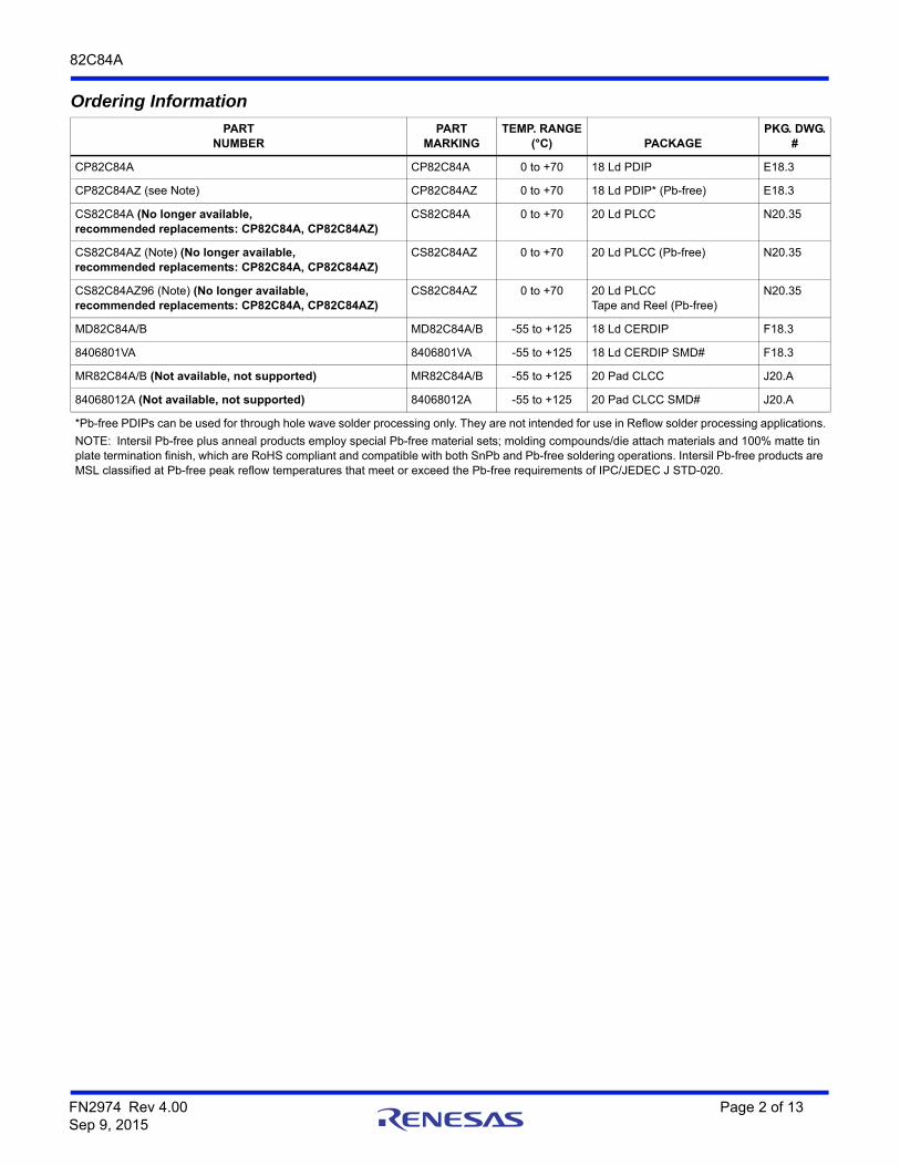
Ordering Information
PARTNUMBER
PARTMARKING
TEMP. RANGE(°C) PACKAGE
PKG. DWG.#
CP82C84A CP82C84A 0 to +70 18 Ld PDIP E18.3
CP82C84AZ (see Note) CP82C84AZ 0 to +70 18 Ld PDIP* (Pb-free) E18.3
CS82C84A (No longer available, recommended replacements: CP82C84A, CP82C84AZ)
CS82C84A 0 to +70 20 Ld PLCC N20.35
CS82C84AZ (Note) (No longer available, recommended replacements: CP82C84A, CP82C84AZ)
CS82C84AZ 0 to +70 20 Ld PLCC (Pb-free) N20.35
CS82C84AZ96 (Note) (No longer available, recommended replacements: CP82C84A, CP82C84AZ)
CS82C84AZ 0 to +70 20 Ld PLCCTape and Reel (Pb-free)
N20.35
MD82C84A/B MD82C84A/B -55 to +125 18 Ld CERDIP F18.3
8406801VA 8406801VA -55 to +125 18 Ld CERDIP SMD# F18.3
MR82C84A/B (Not available, not supported) MR82C84A/B -55 to +125 20 Pad CLCC J20.A
84068012A (Not available, not supported) 84068012A -55 to +125 20 Pad CLCC SMD# J20.A
*Pb-free PDIPs can be used for through hole wave solder processing only. They are not intended for use in Reflow solder processing applications.
NOTE: Intersil Pb-free plus anneal products employ special Pb-free material sets; molding compounds/die attach materials and 100% matte tin plate termination finish, which are RoHS compliant and compatible with both SnPb and Pb-free soldering operations. Intersil Pb-free products are MSL classified at Pb-free peak reflow temperatures that meet or exceed the Pb-free requirements of IPC/JEDEC J STD-020.
FN2974 Rev 4.00 Page 2 of 13Sep 9, 2015

82C84A
Functional Diagram
CONTROL PIN LOGICAL 1 LOGICAL 0
F/C External Clock Crystal Drive
RES Normal Reset
RDY1, RDY2 Bus Ready Bus Not Ready
AEN1, AEN2 Address Disabled Address Enable
ASYNC 1 Stage Ready Synchronization
2 Stage Ready Synchronization
X1
X2
EF1
CSYNC
RDY1
RDY2
11
17
16
13
14
1
4
3
6
7
15
RESET
OSC
PCLK
CLK
READY
XTALOSCILLATOR
CKD Q
FF1
CK
D
CKD Q
FF2
Q
12
2
8
5
10RES
F/C
AEN1
AEN2
ASYNC
SYNC 2
SYNC 3
FN2974 Rev 4.00 Page 3 of 13Sep 9, 2015

82C84A
Pin Description
SYMBOL NUMBER TYPE DESCRIPTION
AEN1, AEN2
3, 7 I ADDRESS ENABLE: AEN is an active LOW signal. AEN serves to qualify its respective Bus Ready Signal (RDY1 or RDY2). AEN1 validates RDY1 while AEN2 validates RDY2. Two AEN signal inputs are useful in system configurations which permit the processor to access two Multi-Master System Busses. In non-Multi-Master configurations, the AEN signal inputs are tied true (LOW).
RDY1, RDY2
4, 6 I BUS READY (Transfer Complete). RDY is an active HIGH signal which is an indication from a device located on the system data bus that data has been received, or is available RDY1 is qualified by AEN1 while RDY2 is qualified by AEN2.
ASYNC 15 I READY SYNCHRONIZATION SELECT: ASYNC is an input which defines the synchronization mode of the READY logic. When ASYNC is low, two stages of READY synchronization are provided. When ASYNC is left open or HIGH, a single stage of READY synchronization is provided.
READY 5 O READY: READY is an active HIGH signal which is the synchronized RDY signal input. READY is cleared after the guaranteed hold time to the processor has been met.
X1, X2 17, 16 I O CRYSTAL IN: X1 and X2 are the pins to which a crystal is attached. The crystal frequency is 3 times the desired processor clock frequency, (Note 1).
F/C 13 I FREQUENCY/CRYSTAL SELECT: F/C is a strapping option. When strapped LOW. F/C permits the processor’s clock to be generated by the crystal. When F/C is strapped HIGH, CLK is generated for the EFI input, (Note 1).
EFI 14 I EXTERNAL FREQUENCY IN: When F/C is strapped HIGH, CLK is generated from the input frequency appearing on this pin. The input signal is a square wave 3 times the frequency of the desired CLK output.
CLK 8 O PROCESSOR CLOCK: CLK is the clock output used by the processor and all devices which directly connect to the processor’s local bus. CLK has an output frequency which is 1/3 of the crystal or EFI input frequency and a 1/3 duty cycle.
PCLK 2 O PERIPHERAL CLOCK: PCLK is a peripheral clock signal whose output frequency is 1/2 that of CLK and has a 50% duty cycle.
OSC 12 O OSCILLATOR OUTPUT: OSC is the output of the internal oscillator circuitry. Its frequency is equal to that of the crystal.
RES 11 I RESET IN: RES is an active LOW signal which is used to generate RESET. The 82C84A provides a Schmitt trigger input so that an RC connection can be used to establish the power-up reset of proper duration.
RESET 10 O RESET: RESET is an active HIGH signal which is used to reset the 80C86 family processors. Its timing characteristics are determined by RES.
CSYNC 1 I CLOCK SYNCHRONIZATION: CSYNC is an active HIGH signal which allows multiple 82C84As to be synchronized to provide clocks that are in phase. When CSYNC is HIGH the internal counters are reset. When CSYNC goes LOW the internal counters are allowed to resume counting. CSYNC needs to be externally synchronized to EFI. When using the internal oscillator CSYNC should be hardwired to ground.
GND 9 Ground
VCC 18 VCC: The +5V power supply pin. A 0.1F capacitor between VCC and GND is recommended for decoupling.
NOTE:
1. If the crystal inputs are not used X1 must be tied to VCC or GND and X2 should be left open.
FN2974 Rev 4.00 Page 4 of 13Sep 9, 2015

82C84A
Functional Description
Oscillator
The oscillator circuit of the 82C84A is designed primarily for use with an external parallel resonant, fundamental mode crystal from which the basic operating frequency is derived.
The crystal frequency should be selected at three times the required CPU clock. X1 and X2 are the two crystal input crystal connections. For the most stable operation of the oscillator (OSC) output circuit, two capacitors (C1 = C2) as shown in the waveform figures are recommended. The output of the oscillator is buffered and brought out on OSC so that other system timing signals can be derived from this stable, crystal-controlled source.
Capacitors C1, C2 are chosen such that their combined capacitance
matches the load capacitance as specified by the crystal manufacturer. This ensures operation within the frequency tolerance specified by the crystal manufacturer.
Clock Generator
The clock generator consists of a synchronous divide-by- three counter with a special clear input that inhibits the counting. This clear input (CSYNC) allows the output clock to be synchronized with an external event (such as another 82C84A clock). It is necessary to synchronize the CSYNC input to the EFI clock external to the 82C84A. This is accomplished with two flip-flops. (See Figure 1). The counter output is a 33% duty cycle clock at one-third the input frequency.
NOTE: The F/C input is a strapping pin that selects either the crystaloscillator or the EFI input as the clock for the 3 counter. Ifthe EFI input is selected as the clock source, the oscillatorsection can be used independently for another clock source.Output is taken from OSC.
Clock Outputs
The CLK output is a 33% duty cycle clock driver designed to drive the 80C86, 80C88 processors directly. PCLK is a peripheral clock signal whose output frequency is 1/2 that of CLK. PCLK has a 50% duty cycle.
Reset Logic
The reset logic provides a Schmitt trigger input (RES) and a synchronizing flip-flop to generate the reset timing. The reset signal is synchronized to the falling edge of CLK. A simple RC network can be used to provide power-on reset by utilizing this function of the 82C84A.
READY Synchronization
Two READY input (RDY1, RDY2) are provided to accommodate two system busses. Each input has a qualifier (AEN1 and AEN2, respectively). The AEN signals validate their respective RDY signals. If a Multi-Master system is not being used the AEN pin should be tied LOW.
Synchronization is required for all asynchronous active-going edges of either RDY input to guarantee that the RDY setup and hold times are met. Inactive-going edges of RDY in normally ready systems do not require synchronization but must satisfy RDY setup and hold as a matter of proper system design.
The ASYNC input defines two modes of READY synchronization operation.
When ASYNC is LOW, two stages of synchronization are provided for active READY input signals. Positive-going asynchronous READY inputs will first be synchronized to flip-flop one of the rising edge of CLK (requiring a setup time tR1VCH) and the synchronized to flip-flop two at the next falling edge of CLK, after which time the READY output will go active (HIGH). Negative-going asynchronous READY inputs will be synchronized directly to flip-flop two at the falling edge of CLK, after which the READY output will go inactive. This mode of operation is intended for use by asynchronous (normally not ready) devices in the system which cannot be guaranteed by design to meet the required RDY setup timing, TR1VCL, on each bus cycle.
When ASYNC is high or left open, the first READY flip-flop is bypassed in the READY synchronization logic. READY inputs are synchronized by flip-flop two on the falling edge of CLK before they are presented to the processor. This mode is available for synchronous devices that can be guaranteed to meet the required RDY setup time.
ASYNC can be changed on every bus cycle to select the appropriate mode of synchronization for each device in the system.
TABLE 1. CRYSTAL SPECIFICATIONS
PARAMETER TYPICAL CRYSTAL SPEC
Frequency 2.4 - 25MHz, Fundamental, “AT” cut
Type of Operation Parallel
Unwanted Modes 6dB (Minimum)
Load Capacitance 18 - 32pF
CT = C1 x C2C1 + C2---------------------- (Including stray capacitance)
FN2974 Rev 4.00 Page 5 of 13Sep 9, 2015

82C84A
EFI
EFI
82C84A
CSYNC
(TO OTHER 82C84As)
CLOCKSYNCHRONIZE
D Q
>
D
Q>
FIGURE 1. CSYNC SYNCHRONIZATION
NOTE: If EFI input is used, then crystal input X1 must be tied to VCC or GND and X2 should be left open. If the crystal inputs are used,then EFI should be tied to VCC or GND.
FN2974 Rev 4.00 Page 6 of 13Sep 9, 2015

82C84A
Absolute Maximum Ratings Thermal Information
Supply Voltage . . . . . . . . . . . . . . . . . . . . . . . . . . . . . . . . . . . . . +8.0VInput, Output or I/O Voltage . . . . . . . . . . . . GND -0.5V to VCC +0.5VESD Classification . . . . . . . . . . . . . . . . . . . . . . . . . . . . . . . . . Class 1
Operating ConditionsOperating Voltage Range. . . . . . . . . . . . . . . . . . . . . . +4.5V to +5.5VOperating Temperature Range
C82C84A . . . . . . . . . . . . . . . . . . . . . . . . . . . . . . . . . 0oC to +70oCI82C84A . . . . . . . . . . . . . . . . . . . . . . . . . . . . . . . . -40oC to +85oCM82C84A . . . . . . . . . . . . . . . . . . . . . . . . . . . . . . -55oC to +125oC
Thermal Resistance. . . . . . . . . . . . . . . . . JA (oC/W) JC (oC/W)
CERDIP Package. . . . . . . . . . . . . . . . . 80 20CLCC Package . . . . . . . . . . . . . . . . . . 95 28PDIP Package* . . . . . . . . . . . . . . . . . . 85 N/APLCC Package. . . . . . . . . . . . . . . . . . . 85 N/A
Storage Temperature Range . . . . . . . . . . . . . . . . . -65oC to +150oCMax Junction Temperature . . . . . . . . . . . . . . . . . . . . . . . . . .+175oCLead Temperature (Soldering 10s) . . . . . . . . . . . . . . . . . . . .+300oC
(PLCC - Lead Tips Only)*Pb-free PDIPs can be used for through hole wave solder processing only. They are not intended for use in Reflow solder processing applications.
Die CharacteristicsGate Count . . . . . . . . . . . . . . . . . . . . . . . . . . . . . . . . . . . . .50 Gates
CAUTION: Stresses above those listed in “Absolute Maximum Ratings” may cause permanent damage to the device. This is a stress only rating and operation of thedevice at these or any other conditions above those indicated in the operational sections of this specification is not implied.
DC Electrical Specifications VCC = +5.0V10%,
TA = 0oC to +70oC (C82C84A),
TA = -40oC to +85oC (I82C84A),
TA = -55oC to +125oC (M82C84A)
SYMBOL PARAMETER MIN MAX UNITS TEST CONDITIONS
VIH Logical One Input Voltage 2.02.2
- VV
C82C84A, I82C84M82C84A, Notes 1, 2
VIL Logical Zero Input Voltage - 0.8 V Notes 1, 2, 3
VIHR Reset Input High Voltage VCC -0.8 - V
VILR Reset Input Low Voltage - 0.5 V
VT+ - VT- Reset Input Hysteresis 0.2 VCC - -
VOH Logical One Output Current VCC -0.4 - V IOH = -4.0mA for CLK OutputIOH = -2.5mA for All Others
VOL Logical Zero Output Voltage - 0.4 V IOL = +4.0mA for CLK OutputIOL = +2.5mA for All Others
II Input Leakage Current -1.0 1.0 A VIN = VCC or GND except ASYNC, X1: (Note 4)
ICCOP Operating Power Supply Current - 40 mA Crystal Frequency = 25MHzOutputs Open, Note 5
NOTES:
1. F/C is a strap option and should be held either 0.8V or 2.2V. Does not apply to X1 or X2 pins.
2. Due to test equipment limitations related to noise, the actual tested value may differ from that specified, but the specified limit isguaranteed.
3. CSYNC pin is tested with VIL 0.8V.
4. ASYNC pin includes an internal 17.5k nominal pull-up resistor. For ASYNC input at GND, ASYNC input leakage current = 300Anominal, X1 - crystal feedback input.
5. f = 25MHz may be tested using the extrapolated value based on measurements taken at f = 2MHz and f = 10MHz.
Capacitance TA = +25oC
SYMBOL PARAMETER TYPICAL UNITS TEST CONDITIONS
CIN Input Capacitance 10 pF FREQ = 1MHz, all measurements arereferenced to device GND
COUT Output Capacitance 15 pF
FN2974 Rev 4.00 Page 7 of 13Sep 9, 2015

82C84A
AC Electrical Specifications VCC = +5V 10%,
TA = 0oC to +70oC (C82C84A),
TA = -40oC to +85oC (I82C84A),
TA = -55oC to +125oC (M82C84A)
SYMBOL PARAMETER
LIMITS
UNITS
(NOTE 1)TEST
CONDITIONS MIN MAX
TIMING REQUIREMENTS
(1) TEHEL External Frequency HIGH Time 13 - ns 90%-90% VIN
(2) TELEH External Frequency LOW Time 13 - ns 10%-10% VIN
(3) TELEL EFI Period 36 - ns
XTAL Frequency 2.4 25 MHz Note 2
(4) TR2VCL RDY1, RDY2 Active Setup to CLK 35 - ns ASYNC = HIGH
(5) TR1VCH RDY1, RDY2 Active Setup to CLK 35 - ns ASYNC = LOW
(6) TR1VCL RDY1, RDY2 Inactive Setup to CLK 35 - ns
(7) TCLR1X RDY1, RDY2 Hold to CLK 0 - ns
(8) TAYVCL ASYNC Setup to CLK 50 - ns
(9) TCLAYX ASYNC Hold to CLK 0 - ns
(10) TA1VR1V AEN1, AEN2 Setup to RDY1, RDY2 15 - ns
(11) TCLA1X AEN1, AEN2 Hold to CLK 0 - ns
(12) TYHEH CSYNC Setup to EFI 20 - ns
(13) TEHYL CSYNC Hold to EFI 20 - ns
(14) TYHYL CSYNC Width 2 TELEL - ns
(15) TI1HCL RES Setup to CLK 65 - ns Note 3
(16) TCLI1H RES Hold to CLK 20 - ns Note 3
TIMING RESPONSES
(17) TCLCL CLK Cycle Period 125 - ns Note 6
(18) TCHCL CLK HIGH Time (1/3 TCLCL) +2.0 - ns Note 6
(19) TCLCH CLK LOW Time (2/3 TCLCL) -15.0 - ns Note 6
(20)(21)
TCH1CH2TCL2CL1
CLK Rise or Fall Time - 10 ns 1.0V to 3.0V
(22) TPHPL PCLK HIGH Time TCLCL-20 - ns Note 6
(23) TPLPH PCLK LOW Time TCLCL-20 - ns Note 6
(24) TRYLCL Ready Inactive to CLK (See Note 4) -8 - ns Note 4
(25) TRYHCH Ready Active to CLK (See Note 3) (2/3 TCLCL) -15.0 - ns Note 5
(26) TCLIL CLK to Reset Delay - 40 ns
(27) TCLPH CLK to PCLK HIGH Delay - 22 ns
(28) TCLPL CLK to PCLK LOW Delay - 22 ns
(29) TOLCH OSC to CLK HIGH Delay -5 22 ns
(30) TOLCL OSC to CLK LOW Delay 2 35 ns
NOTES:
1. Tested as follows: f = 2.4MHz, VIH = 2.6V, VIL = 0.4V, CL = 50pF, VOH 1.5V, VOL 1.5V, unless otherwise specified. RES and F/C must switch between 0.4V and VCC -0.4V. Input rise and fall times driven at 1ns/V. VIL VIL (max) - 0.4V for CSYNC pin. VCC = 4.5V and 5.5V.
2. Tested using EFI or X1 input pin.
3. Setup and hold necessary only to guarantee recognition at next clock.
4. Applies only to T2 states.
5. Applies only to T3 TW states.
6. Tested with EFI input frequency = 4.2MHz.
FN2974 Rev 4.00 Page 8 of 13Sep 9, 2015

82C84A
Timing Waveforms
NOTE: All timing measurements are made at 1.5V, unless otherwise noted.
FIGURE 2. WAVEFORMS FOR CLOCKS AND RESETS SIGNALS
FIGURE 3. WAVEFORMS FOR READY SIGNALS (FOR ASYNCHRONOUS DEVICES)
FIGURE 4. WAVEFORMS FOR READY SIGNALS (FOR SYNCHRONOUS DEVICES)
tEHYL(13)
NAME
EFI
OSC
CLK
PCLK
CSYNC
RES
RESET
I/O
I
O
O
O
O
I
I
tYHYL(14)
(12)tYHEH
(20)tCH1CH2
(29)tOLCH
tELEL(3)
(30)tOLCL
(21)tCL2CL1
(27)tCLPH
(23)tPLPH
tCLI1H(16)
tCLCH(19)
(17) tCLCL
tCLIL(26)
(28)tCLPL
(18)tCHCL
(1) tEHEL(2)tELEH
tPHPL(22)
tI1HCL(15)
tCLR1XtR1VCH
(5)
tA1VR1V
(7)
(10)
tAYVCL(8)
tCLAYX (9)
(25)tRYHCH
(11)
(24) tRYLCL
tCLA1X
(7)tCLR1X
tR1VCL(6)
CLK
RDY1, 2
AEN1, 2
ASYNC
READY
CLK
RDY 1, 2
READY
ASYNC
AEN1, 2
(25)tRYHCH
(24)tRYLCL
tCLR1X
(8)
(4)(7)
(9)
(11)
(7)
(6)
(10)
tR1VCL
tCLR1X
tCLA1X
tR1VCL
tAYVCL
tCLAYX
tA1VRIV
FN2974 Rev 4.00 Page 9 of 13Sep 9, 2015
82C84A
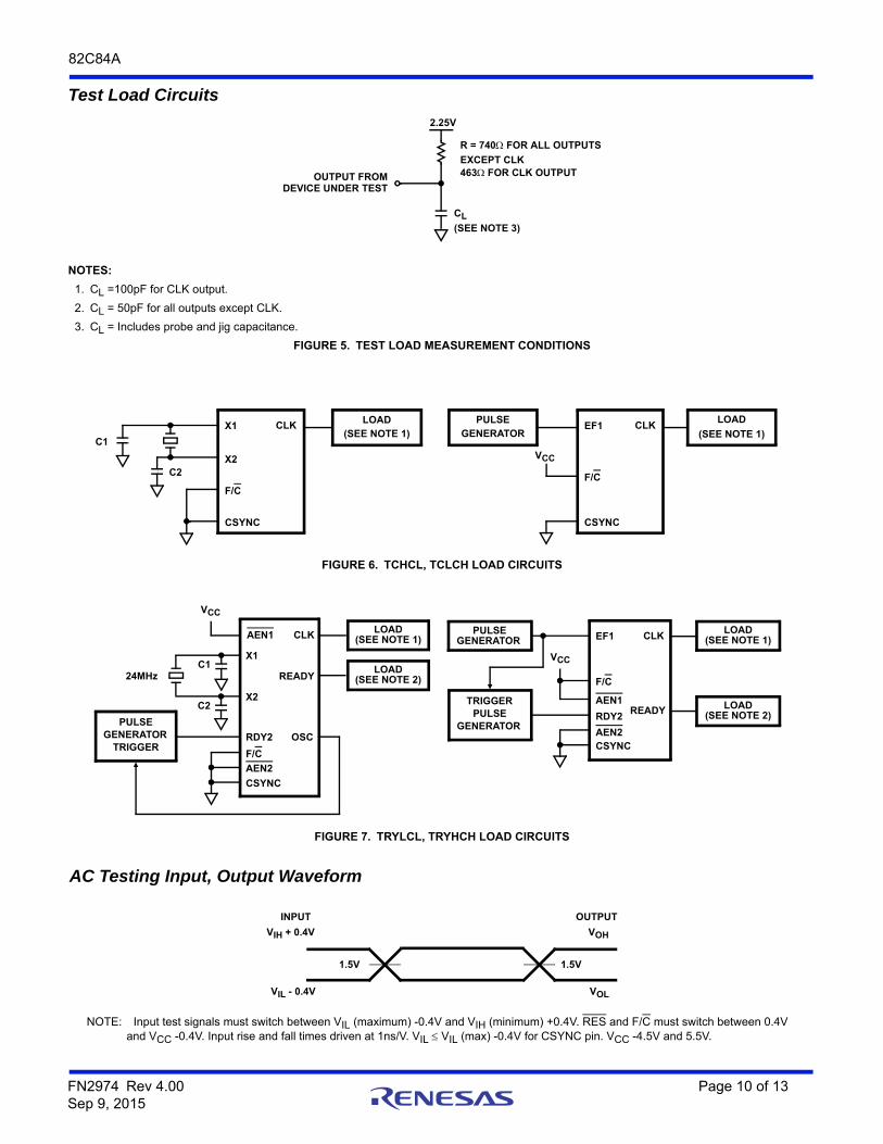
AC Testing Input, Output Waveform
Test Load Circuits
NOTES:
1. CL =100pF for CLK output.
2. CL = 50pF for all outputs except CLK.
3. CL = Includes probe and jig capacitance.
FIGURE 5. TEST LOAD MEASUREMENT CONDITIONS
FIGURE 6. TCHCL, TCLCH LOAD CIRCUITS
FIGURE 7. TRYLCL, TRYHCH LOAD CIRCUITS
CL
OUTPUT FROMDEVICE UNDER TEST
(SEE NOTE 3)
R = 740 FOR ALL OUTPUTS
EXCEPT CLK463 FOR CLK OUTPUT
2.25V
C1
C2
X1
X2
CSYNC
CLK LOAD(SEE NOTE 1)
F/C
EF1
CSYNC
CLKLOAD
(SEE NOTE 1)
F/C
VCC
PULSEGENERATOR
C1
C2
X1
X2
CLKLOAD
(SEE NOTE 1)
LOAD(SEE NOTE 2)
CSYNC
F/C
AEN2
PULSEGENERATOR
TRIGGER
VCC
24MHz READY
OSC
AEN1
RDY2
EF1 CLKLOAD
(SEE NOTE 1)
F/C
VCC
PULSEGENERATOR
CSYNC
RDY2
AEN2
LOAD(SEE NOTE 2)
AEN1READY
TRIGGERPULSE
GENERATOR
1.5V 1.5V
VOLVIL - 0.4V
INPUT
VIH + 0.4V
OUTPUT
VOH
NOTE: Input test signals must switch between VIL (maximum) -0.4V and VIH (minimum) +0.4V. RES and F/C must switch between 0.4V and VCC -0.4V. Input rise and fall times driven at 1ns/V. VIL VIL (max) -0.4V for CSYNC pin. VCC -4.5V and 5.5V.
FN2974 Rev 4.00 Page 10 of 13Sep 9, 2015
82C84A
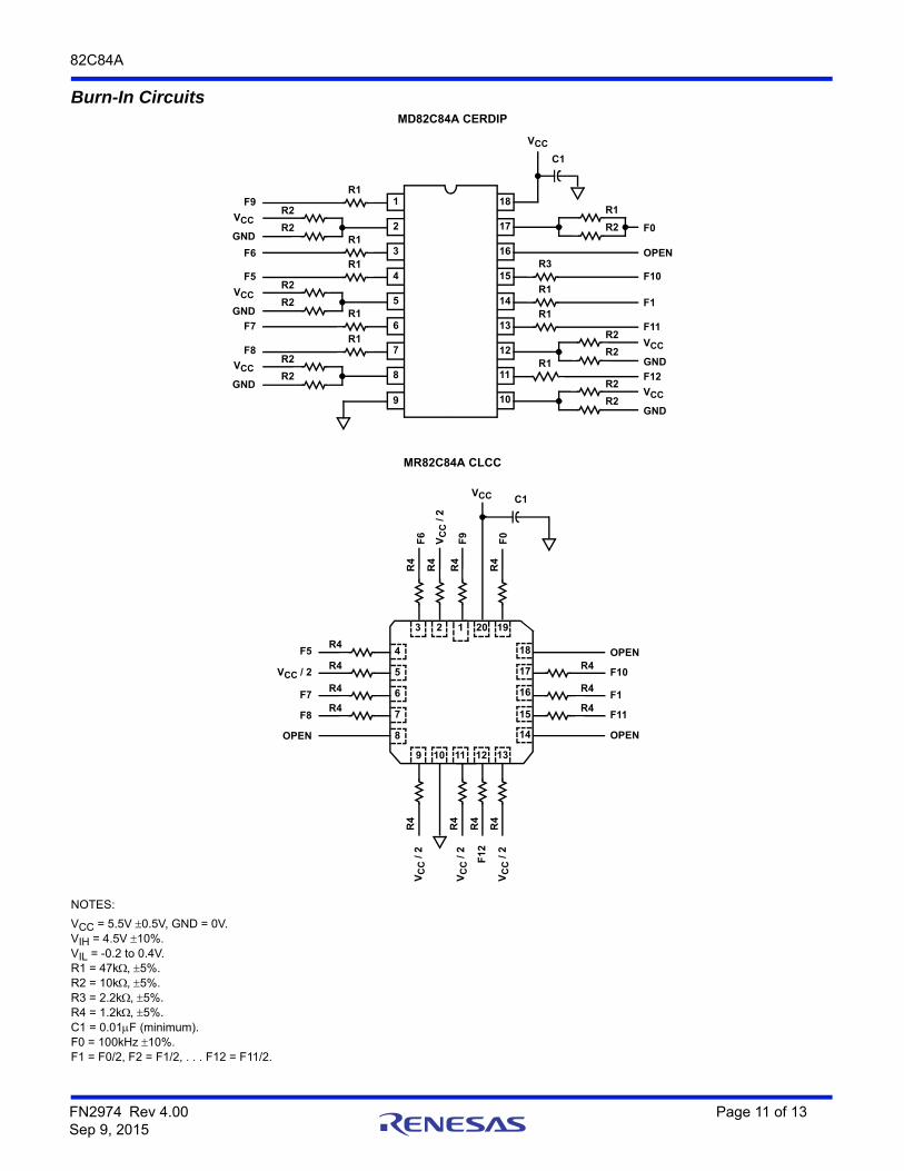
Burn-In CircuitsMD82C84A CERDIP
MR82C84A CLCC
NOTES:
VCC = 5.5V 0.5V, GND = 0V.VIH = 4.5V 10%.VIL = -0.2 to 0.4V.R1 = 47k, 5%.R2 = 10k, 5%.R3 = 2.2k, 5%.R4 = 1.2k, 5%.C1 = 0.01F (minimum).F0 = 100kHz 10%.F1 = F0/2, F2 = F1/2, . . . F12 = F11/2.
10
11
12
13
14
15
16
17
18
9
8
7
6
5
4
3
2
1
R2
R2
R1
R1
R1
R1
R1
R2
R2
R2
R2
R1
R2
R2
R2
R2
R2
R1
R1
R1
R3
VCC
C1
VCC
GND
VCC
GND
F11
F1
F10
OPEN
F0
F12VCC
GND
VCC
GND
VCC
GND
F9
F6
F5
F7
F8
4
5
6
7
8
9 10 11 12 13
3 2 1 20 19
15
14
18
17
16
VCC C1
R4
R4
R4
R4
R4
R4
R4
OPEN
F8
F7
VCC / 2
F5
R4
R4
R4
R4
VC
C /
2
F1
2
VC
C /
2
VC
C /
2
OPEN
F11
F1
F10
OPEN
R4
F0
R4
R4
R4
F9
VC
C /
2
F6
FN2974 Rev 4.00 Page 11 of 13Sep 9, 2015

82C84A
Die Characteristics
DIE DIMENSIONS:66.1 x 70.5 x 191mils
METALLIZATION:Type: Si - AIThickness: 11kÅ 1kÅ
GLASSIVATION:Type: SiO2Thickness: 8kÅ 1kÅ
WORST CASE CURRENT DENSITY:1.42 x 10⁵ A/cm2
Metallization Mask Layout
82C84A
AEN1 PCLK CSYNC VCC X1
RDY1
READY
RDY2
AEN2
CLK
GND RESET RES OSC
X2
ASYNC
EFI
F/C
FN2974 Rev 4.00 Page 12 of 13Sep 9, 2015
82C84A
Intersil products are manufactured, assembled and tested utilizing ISO9001 quality systems as notedin the quality certifications found at www.intersil.com/en/support/qualandreliability.html
Intersil products are sold by description only. Intersil may modify the circuit design and/or specifications of products at any time without notice, provided that such modification does not, in Intersil's sole judgment, affect the form, fit or function of the product. Accordingly, the reader is cautioned to verify that datasheets are current before placing orders. Information furnished by Intersil is believed to be accurate and reliable. However, no responsibility is assumed by Intersil or its subsidiaries for its use; nor for any infringements of patents or other rights of third parties which may result from its use. No license is granted by implication or otherwise under any patent or patent rights of Intersil or its subsidiaries.
For information regarding Intersil Corporation and its products, see www.intersil.com
For additional products, see www.intersil.com/en/products.html
© Copyright Intersil Americas LLC 1997-2015. All Rights Reserved.All trademarks and registered trademarks are the property of their respective owners.
About IntersilIntersil Corporation is a leading provider of innovative power management and precision analog solutions. The company's products address some of the largest markets within the industrial and infrastructure, mobile computing and high-end consumer markets.
For the most updated datasheet, application notes, related documentation and related parts, please see the respective product information page found at www.intersil.com.
You may report errors or suggestions for improving this datasheet by visiting www.intersil.com/ask.
Reliability reports are also available from our website at www.intersil.com/support
Revision HistoryThe revision history provided is for informational purposes only and is believed to be accurate, but not warranted. Please go to the web to make sure that you have the latest revision.
DATE REVISION CHANGE
September 9, 2015 FN2974.4 Updated Ordering Information Table and moved from page 1 to page 2.Added Revision History and About Intersil sections.
FN2974 Rev 4.00 Page 13 of 13Sep 9, 2015