datasheet - l7983 - 60 v, 300 ma synchronous step-down
TRANSCRIPT

Features• 3.5 V to 60 V operating input voltage• Fixed output voltage (3.3 V and 5 V) or adjustable from 0.85 V to VIN
• 300 mA DC output current• Dynamic low consumption mode to low noise mode selection• 10 µA operating quiescent current (L7983PU33R, VIN > 24 V, LCM)• 2.3 µA shutdown current• 200 kHz to 2.2 MHz programmable switching frequency• Optional spread spectrum (dithering)• Internal soft-start• Enable / adjustable UVLO threshold• Synchronization to external clock• Internal compensation network• Internal current limiting• Overvoltage protection• Output voltage sequencing• Thermal shutdown
Applications• Designed for 12 V, 24 V and 48 V buses• Battery powered applications• Decentralized intelligent nodes• Fail safe system• Sensors and low noise applications (LNM)
DescriptionThe L7983 device is a step-down monolithic switching regulator able to deliver up to300 mA DC based on peak current mode architecture.
The output voltage adjustability ranges from 0.85 V to VIN. The wide input voltagerange and adjustable UVLO threshold meet the specification for the 12 V, 24 V and48 V industrial bus standards.
The “Low Consumption Mode” (LCM) is designed for applications active during idlemode, so it maximizes the efficiency at light load with controlled output voltage ripple.The “Low Noise Mode” (LNM) makes the switching frequency constant overloadcurrent range, meeting the low noise application specification. The L7983 supportsdynamic LCM to LNM transition.
The soft-start time is internally fixed and the output voltage supervisor manages thereset phase for any digital load (microcontroller, FPGA, etc.).
The internal compensation network features high noise immunity, simple design andsaves on the component cost.
The RST open collector output can also implement output voltage sequencing duringthe power-up phase.
Maturity status link
L7983
60 V, 300 mA synchronous step-down switching regulator with 10 µA quiescent current
L7983
Datasheet
DS13354 - Rev 1 - October 2020For further information contact your local STMicroelectronics sales office.
www.st.com

The synchronous rectification, designed for high efficiency at medium - heavy load,and the high switching frequency capability make the size of the application compact.
Pulse-by-pulse current sensing on both power elements implements an effectiveconstant current protection.
L7983
DS13354 - Rev 1 page 2/43

1 Application schematic and block diagram
1.1 Application circuit
Figure 1. Typical application circuit
VIN
EN/UVLO
FSW
VCC
LX
VOUT(FB)
VBIAS
RST
LNM/LCM GNDEP
VIN
GNDGND
VOUT
RESETL7983
Figure 2. Block diagram
VIN
EN/UVLO
FSW
VCC
LNM/LCM
RST
LX
VOUT(FB)
VBIAS
GND
LOGICand
CONTROLDRIVER
andANTI XC
VIN MONITOR UVLO
+
-LDO
+
-
+
-
+
-gm
BIASand
REFERENCE
VREF
SOFT-STARTCONTROL
VMAX
VMIN
+
-
+
- SENSESENSE
SLOPE
IPK
VIN
LX
LX
FSW SET
HS MOS
LS MOS
OTPMONITOR
PWM
ENABLE
ENABLE
END SS
END SS
CLOCK
CLOCK
COMP
+-OVP
SYNCH
+
-
IVYLX
VCC
VCC
+
-ZCDLX
++
CLOCK
L7983Application schematic and block diagram
DS13354 - Rev 1 page 3/43

2 Pin settings
Figure 3. Pin connection (top view)
1VOUT/FB
2
3
4
5
EXPOSEDPAD TO
GND
10
9
8
7
6
VBIAS
VCC
FSW
LNM/LCM
GND
LX
VIN
EN/UVLO
RST
Table 1. Pin description
N° Pin Description
1 VOUT/FB
Output voltage sensing. This pin operates as VOUT or FB accordingly withselected part number:• VOUT is output voltage sensing with selected internal voltage divider.• FB is output voltage sensing with external resistor divider.
2 VBIAS
Input supply of the integrated LDO. Typically connected to the regulated outputvoltage or an auxiliary rail to increase the efficiency at light load. Connect to GNDif not used or bypass with a 100 nF ceramic capacitor if supplied by the outputvoltage or by an auxiliary rail.
3 VCCOutput of the integrated LDO that supplies the embedded analog circuitry.
Connect a ceramic capacitor (470 nF typ.) to filter internal voltage reference.
4 FSW Switching frequency programming pin. Connect an external resistor to VCC orGND.
5 LNM/LCMDynamic pin selection between Low Consumption Mode (LCM, active low) andLow Noise Mode operation (LNM, active high). This pin can also be used forsynchronization with an external clock (clock-in function).
6 RSTActive low open collector output for output monitoring and power-up resetsequencing. RST is driven in low impedance when the output voltage is out ofregulation and released once the output voltage becomes valid.
7 EN/UVLO Active high enable pin, VIN compatible. It can be exploited with an externalresistor divider to adjust the input undervoltage lockout (UVLO).
8 VIN DC input voltage
9 LX Switching node
10 GND Ground
-- E.P. Exposed pad must be connected to GND
L7983Pin settings
DS13354 - Rev 1 page 4/43

3 Absolute maximum ratings
Stressing the device above the ratings listed in Table 2 may cause permanent damage to the device. These arestress ratings only and operation of the device at these or any other conditions above those indicated in theoperating sections of this specification is not implied. Exposure to absolute maximum rating conditions may affectdevice reliability.
Table 2. Absolute maximum ratings
Symbol Description Min. Max. Unit
VIN See Table 1 -0.3 63 V
VCC -0.3 VIN + 0.3 ormax. 3.6 V
EN/UVLO-0.3 VIN + 0.3
V
RST V
LX -0.3 VIN + 0.3 V
VBIAS -0.3 VIN + 0.3 ormax. 14 V
VOUT/FB-0.3 5.5
V
LNM/LCM V
FSW -0.3 VCC + 0.3 V
IHS, ILS High-side / low-side RMS switch current 0.3 A
TJ Operating temperature range -40 150
°CTSTG Storage temperature range -65 150
TLEAD Lead temperature (soldering 10 sec.) 260
3.1 Thermal characteristics
Table 3. Thermal data
Symbol Parameter Value Unit
RthJAThermal resistance junction to ambient (device soldered on a
standard demonstration board) 50 °C/W
3.2 ESD protection
Table 4. ESD performance
Symbol Test conditions Value Unit
ESDHBM 2 kV
CDM 500 V
L7983Absolute maximum ratings
DS13354 - Rev 1 page 5/43

3.3 Operating conditions
Table 5. Recommended operating conditions
Symbol ParameterValue
UnitMin. Typ. Max.
VIN Power supply voltage 3.5 60 V
VBIAS 0 14 V
L7983Operating conditions
DS13354 - Rev 1 page 6/43

4 Electrical characteristics
TJ = 25 °C, VIN = 24 V, VEN/UVLO = VIN, LNM selected, fSW = 1 MHz unless otherwise specified.
Table 6. Electrical characteristics
Symbol Parameter Test Condition Min. Typ. Max. Unit
Turn on and power section characteristics
VINH VIN turn-on VIN rising 2.6 2.8 3.0
VVINL VIN turn-off
VIN falling 2.5 2.7 2.9
Hysteresis 0.1
VWAKEUPH Wake-up ON threshold VEN rising 0.7
V
VWAKEUPL Wake-up OFF threshold VEN falling 0.2
VENH Enable ON threshold VEN rising 1.1 1.2 1.3
VENL Enable OFF thresholdVEN falling 0.9 1.0 1.1
Hysteresis 0.2
IPK Peak current limitDuty cycle < 20% (1) 0.42 0.47 0.52
A
Duty cycle = 100%, closed loop operation (1) 0.35 0.39 0.43
IVY Valley current limit (1) 0.43 0.52 0.61
ISKIP Skip current limit (1) 0.08
INEG Reverse current limit LNM selected, VFB = 0.9 V (1) - 0.15
HS RDSON HS MOS ON resistance ILX = 0.2 A 1.9 2.5Ω
LS RDSON LS MOS ON resistance ILX = 0.2 A 0.85 1.2
fSW Selected switching frequency
RFSW = 5.6 kΩ 450 500 550
kHzRFSW = 0 Ω 900 1000 1100
RFSW = 56 kΩ 1980 2200 2420
D Duty cycle 0 100 %
tON MIN Minimum HS MOS on-time 60 ns
tSS Internal soft-start time 1.3 2 2.7 ms
VCC and VBIAS
VCC LDO output voltageVBIAS = GND 2.9 3.3 3.6
VVBIAS = 5 V 2.9 3.3 3.6
SWO Switchover threshold VBIAS increasing 3.2 V
Hysteresis 0.075 V
Power consumption
ISHTDWN Shutdown current from VIN VEN/UVLO = GND 2.3 3.2
µAIQVIN
Quiescent current from VIN, LCM(refer to Section 5.5 VCC andswitchover)
VBIAS = 5 V, VOUT = 1.05 * VREF(2) 3 6
VBIAS = GND, VOUT = 1.05 * VREF(2) 35 50
Quiescent current from VIN, LNMVBIAS = 5 V, VOUT = 1.05 * VREF 170 205
VBIAS = GND, VOUT = 1.05 * VREF 1300 1500
L7983Electrical characteristics
DS13354 - Rev 1 page 7/43

Symbol Parameter Test Condition Min. Typ. Max. Unit
IQVBIAS Quiescent current from VBIASLCM, VBIAS = 5 V, VOUT = 1.05 * VREF(2)
µA37 50
LNM, VBIAS = 5 V, VOUT = 1.05 * VREF 1200 1400
Voltage reference and OVP
VREF
Voltage feedback, L7983PURTJ = 25 °C 0.844 0.850 0.856
V
-40 °C ≤ TJ ≤ 125 °C (3) 0.840 0.850 0.860
Voltage feedback, L7983PU33RTJ = 25 °C 3.267 3.300 3.333
-40 °C ≤ TJ ≤ 125 °C (3) 3.250 3.300 3.350
Voltage feedback, L7983PU50RTJ = 25 °C 4.950 5.000 5.050
-40 °C ≤ TJ ≤ 125 °C (3) 4.925 5.000 5.075
VOVP Overvoltage trip (VOUT/VREF) 115 120 125 %
VOVP,HYST Overvoltage hysteresis 2 %
Synchronization (clock-in) and LNM/LCM
fCLKIN Synchronization range 180 2400 kHz
VCLKINH CLKIN allowed high level 2 5 V
VCLKINL CLKIN allowed low level 0 1.3 V
VLNM LNM selection level 2 5 V
VLCM LCM selection level 0 1.3 V
TLNM/LCMMinimum allowed delay betweenLNM to LCM or LCM to LNMdynamic selection
14 µs
Reset
VRSTTHRRST release threshold
(VOUT/VREF)
TJ = 25 °C 90 92 94
%-40 °C ≤ TJ ≤ 125 °C (3) 88 96
VRSTHYST RST hysteresis 2
TRSTDLYDelay from VRSTTHR thresholddetection and RST pin release 2.0 ms
VRSTLOW RST open collector outputVOUT/VREF = 80%, 4 mA sinking current 0.3 0.4
V2 < VIN < VINH, 4 mA sinking current 0.5 0.8
IRSTLKG RST leakage current VIN = 60 V, VOUT/VREF = 110% 0.2 µA
Thermal shutdown
TSHDWN Thermal shutdown threshold (4) 165°C
THYS Thermal shutdown hysteresis (4) 30
1. Parameter tested in static condition during testing phase. Parameter value may change over dynamicapplication condition.
2. LCM enables SLEEP mode at light load.3. Specifications in the -40 to +125 °C temperature range are assured by characterization and statistical
correlation.4. Not tested in production.
L7983Electrical characteristics
DS13354 - Rev 1 page 8/43

5 Functional description
The L7983 device is a monolithic step-down (“buck”) DC-DC voltage regulator based on a peak current mode,constant frequency architecture, with integrated control loop compensation network.The main internal blocks are shown in Figure 2 and can be summarized as follows:• Power section, including high-side and low-side power MOSFETs, gate driver and current sensing• Control loop blocks, including the trans-conductor (gm), the PWM comparator and the slope generator• The control logic for low noise mode (LNM) or low consumption mode (LCM) operation selection and
synchronization to external clock• The frequency programming circuitry for device configuration• Input voltage monitor and enable circuit with soft-start management and RST output signal for sequencing
programming• The low drop-out linear regulator (LDO) and switchover block to improve the power conversion efficiency.
The fault management, including the overcurrent (OCP), the overvoltage (OVP) and overtemperature (OTP)protection
5.1 Power section
The L7983 integrates both power MOSFETs for synchronous operation; one P-channel (high-side, HS) and oneN-channel (low-side, LS), optimized for fast switching transition and high efficiency over the entire load range. Thepower stage is designed to deliver a continuous output current up to 0.3 A.The HS MOSFET source is connected to the VIN pin, the LS MOSFET source is connected to the GND pin(power ground). The HS MOSFET drain and LS MOSFET drain are connected together and to the LX pin (seeFigure 2).The L7983 embodies an anti-shoot-through and adaptive deadtime control to minimize low-side body diodeconduction time and consequently reduce power losses. This feature is implemented by comparing LX with HSand LS gate driving voltage.• Following the HS turn-off, the LS MOSFET is suddenly switched on as soon as the voltage at the LX pin
drops• Following the LS turn-off, the HS MOSFET is suddenly switched on as soon as the gate driving voltage of
LS drops
If the current flowing in the inductor is negative (i.e. from VOUT to VIN), the voltage on the LX pin can’t drop afterHS MOS turn-off. A watchdog controller is implemented to allow the LS MOSFET to turn on even in this case,allowing the negative current of the inductor to flow to ground. This mechanism allows the system to regulateeven if the current is negative (if LNM mode is enabled).
5.2 Control loop and voltage programming
The L7983 is based on a constant frequency peak current mode architecture.Thanks to integrated compensation network and slope generation, no additional external components arenecessary for loop stabilization.
L7983Functional description
DS13354 - Rev 1 page 9/43

Figure 4. Control loop block diagram
Res
o
RoRu
Rd
VREF
L
Rc
Cc
Vin
Slopecompensation
Currentsense
PWMComparator
PowerSwitches
FB
Cp
Cu
Vout
Co
HS
LS++ gcs
E/A
Integratedcompensation
Refer to Section 5.7 for further details on power components design.For the adjustable version (L7983PUR), the output voltage can be programmed through an external resistordivider, from 0.85 V up to VIN.The design equation is:
VOUT = 0.85 ∙ 1 + RURD (1)
For the fixed version (L7983PU33R or L7983PU50R), the output voltage programming is achieved by simplyshorting the VOUT(FB) pin to the output capacitor.
L7983Control loop and voltage programming
DS13354 - Rev 1 page 10/43

Figure 5. Output voltage programming - adjustable version
VIN
EN/UVLO
FSW
VCC
LX
VOUT(FB)
VBIAS
RST
LNM/LCM GNDEPRD
RU
Figure 6. Output voltage programming - fixed version
VIN
EN/UVLO
FSW
VCC
LX
VOUT(FB)
VBIAS
RST
LNM/LCM GNDEP
L7983Control loop and voltage programming
DS13354 - Rev 1 page 11/43

5.2.1 LNM/LCM selection and synchronizationDepending on the low-side power MOSFET management, the inductor current can be allowed to reverse or not.The choice can be performed during device operation by acting on the LNM/LCM pin.When the low-noise mode (LNM) operation is selected, by forcing high pin LNM/LCM, the inductor current canreverse. In this way a constant switching frequency is achieved, so limiting the output voltage ripple and providinga prompt transient response.
Figure 7. LNM selected, no load
If the LNM/LCM pin is forced low, the low-consumption mode (LCM) is activated, with the aim of maximizing thelight load efficiency. When LCM is selected, the high-side MOSFET is turned on as soon as the FB pin is sensedlower than VREFLCM, i.e. VREF reference voltage increased by 2% typ.:VREFLCM = VREF ∙ 1,02 typ. (2)
In LCM mode the HS MOS is turned on until ISKIP current is reached, then it is turned-off. The low-side MOSFETis then turned on until one of the following conditions occurs:• The sensed inductor current drops to zero• The switching period (programmed through the FSW pin) has expired and the FB pin is still lower than the
voltage reference. In this case a new switching cycle is performed.
In LCM working mode the regulator switching frequency is load-dependent (i.e. LX pulses can be skipped) withgreater advantage to power conversion efficiency at light load.The following waveforms are showing the switching activity in LCM working mode and different load.
L7983Control loop and voltage programming
DS13354 - Rev 1 page 12/43

Figure 8. LCM selected, no load
Figure 9. LCM selected, 10 mA load
L7983Control loop and voltage programming
DS13354 - Rev 1 page 13/43

Figure 10. LCM selected, 50 mA load
If an external clock is applied on the LNM/LCM pin, the L7983 switching activity is synchronized to the appliedclock and the LNM operation is enabled. The external clock must meet the electrical requirements summarized inTable 7. In case no external clock is detected on LNM/LCM for TLNM/LCM (14 µs typ.), the free running clockprogrammed on pin FSW through RFSW resistor is restored as switching frequency. Refer toSection 5.3 Switching frequency programming and dithering.TLNM/LCM is also the typical delay between LNM to LCM and the opposite transition.
Figure 11. LCM to LNM transition, no load
L7983Control loop and voltage programming
DS13354 - Rev 1 page 14/43

5.3 Switching frequency programming and dithering
The L7983 has one programming pin, FSW (pin 4), which is used to set the regulator free running switchingfrequency.The switching frequency programming feature is performed by selecting the proper 1% accuracy resistor, to bemounted between pin 4 and ground or VCC, as summarized in the following table. The pinstrapping is active onlybefore the soft-start phase to minimize the IC consumption.Refer also to Figure 1 for reference schematic.
Table 7. FSW pin programming resistor
Dithering enabled Dithering disabled
# RVCC [kΩ] RGND [kΩ] Fsw [kHz] (1) # RVCC [kΩ] RGND [kΩ] Fsw [kHz] (1)
1 0 -- 1000 1 -- 0 1000
2 1,8 -- 200 2 -- 1,8 200
3 3,3 -- 400 3 -- 3,3 400
4 5,6 -- 500 4 -- 5,6 500
5 10 -- 700 5 -- 10 700
6 18 -- 1500 6 -- 18 1500
7 33 -- 2000 7 -- 33 2000
8 56 -- 2200 8 -- 56 2200
1. Typical value. Refer to Table 6 for details.
L7983Switching frequency programming and dithering
DS13354 - Rev 1 page 15/43

The dithering function, enabled by connecting the proper RFSW resistor to VCC, is intended to reduce the DC-DCelectromagnetic emissions, with small impact on output voltage ripple.
Figure 12. RVCC = 0 Ω, dithering enabled, no load
Figure 13. RVCC = 0 Ω, dithering enabled, no load. Detail
The internal dithering circuitry changes the switching frequency in the range of ± 5% of the nominal value. Thedevice updates the frequency every clock period by fixed steps:• Ramps up in 63 steps from minimum to maximum switching frequency• Ramps down in 63 steps from maximum to minimum switching frequency
The resulting frequency modulation is almost triangular, with a frequency of:
FDitℎ = FSW126 (3)
L7983Switching frequency programming and dithering
DS13354 - Rev 1 page 16/43

5.4 Enable and Reset
In order to maximize both the EN threshold accuracy and the current consumption, the device implements twodifferent enable thresholds:• The wake-up threshold, VWAKEUPH = 0.5 V typ.• The start-up threshold, VENH = 1.2 V typ.
As soon as the EN pin is detected above VWAKEUPH and VIN voltage is higher than VINH, the regulator turns onthe internal circuitry and waits for the VENH before starting the switching activity. When this occurs, the internalvoltage reference is increased by about 2 ms (typ.) in order to limit the inrush current and perform a smoothoutput capacitor charge.
Figure 14. Turn-on example
L7983Enable and Reset
DS13354 - Rev 1 page 17/43

If the EN pin is forced lower than VENL the switching activity is stopped. The L7983 can further reduce the inputcurrent as soon as EN is forced lower than the VWAKEUPL threshold. When this occurs the input current is reducedto ISHTDWN = 2.3 µA (typ.).
Figure 15. Turn-off example
A divider from VIN can be used to program the input voltage threshold for controlled power-up, as shown inFigure 16.The EN pin is VIN compatible.
Figure 16. Input voltage turn-on threshold programming
VIN
EN/UVLO
FSW
VCC
LX
VOUT(FB)
VBIAS
RST
LNM/LCM GNDEP
During the soft-start, the L7983 is not allowed to sink current from the output, also if LNM operation is selected.This feature is intended to guarantee the proper power-up also in case of output voltage pre-bias condition.Following the L7983 turn-on, if the output voltage (sensed through the VOUT(FB) pin) is detected higher than theVRSTTHR threshold, the RST pin is left floating.During the operation, the RST pin is asserted low if the output voltage is found lower than the VRSTTHR -VRSTHYST threshold, i.e. a typical 2% hysteresis is implemented.
L7983Enable and Reset
DS13354 - Rev 1 page 18/43

In case of overvoltage detection (OVP), the RST pin is asserted low. A 2% hysteresis (typ.) is required beforereleasing RST.
Figure 17. Output voltage and RST behavior
VTHRVTHR-HYST
VOUT
RST
Td
A built-in 2 ms typ. delay is always implemented before releasing RST.
5.5 VCC and switchover
The internal LDO (low drop-out) linear regulator is turned on when VIN is higher than the VINH threshold and ENpin is detected above VWAKEUPH. The output voltage is available on pin VCC, which must be properly bypassed toGND by 470 nF ceramic capacitor. No external load is expected on VCC pin.The switchover function is enabled in case VBIAS is detected higher than the SWO threshold (refer to Table 7).When this occurs, the internal LDO power supply is switched from VIN to VBIAS, so increasing the powerconversion efficiency. This is the typical case when VBIAS is connected to the regulator output.If the programmed output voltage is lower than the SWO threshold and no auxiliary rail lower than VIN isavailable, VBIAS must be connected to GND (refer to Figure 29, Figure 35 and Figure 41 for no load input currentin typical application conditions).
5.6 Fault management
The L7983 fault management is continuously monitoring the inductor current, the output voltage and the devicejunction temperature.Furthermore, thanks to the input UVLO (undervoltage lock-out) circuitry, the switching activity is guaranteed onlywith the proper VIN level. All the protections are auto-recovery.
L7983VCC and switchover
DS13354 - Rev 1 page 19/43

5.6.1 Overcurrent protection (OCP)In normal operation the HS MOS is turned off when the sensed current is equal to programmed current (refer toFigure 2). The maximum available current is limited by the internal OCP (overcurrent protection) comparator,cycle by cycle. The IPK threshold is gradually reduced during the switching period by slope contribution, as shownin Figure 18.
Figure 18. Peak current limit
IPK
ILXTON_min
The inductor current is also monitored during LS MOS on-time. This feature, also known as “valley currentlimitation”, is effective in case of current runaway due to HS MOS minimum on-time limitation and very lowVOUT / VIN ratio. This protection can avoid the HS MOS turn-on if the inductor current, sensed during LS MOSon-time, is higher than the IVY threshold (Figure 19).
Figure 19. Valley current limit
IPK
IVY
TON_min
ILX
L7983Fault management
DS13354 - Rev 1 page 20/43

In LNM mode, the L7983 can sink current from the output. However, to protect the power components, a negativecurrent limit is implemented. If the sensed current is found lower than the INEG threshold, the low-side MOS ispromptly turned off and the high-side one is turned on until the inductor is discharged. When this occurs, the LSMOS is allowed to turn on again.
Figure 20. Negative current limit example
L7983Fault management
DS13354 - Rev 1 page 21/43

5.6.2 Overvoltage protection (OVP)In case the VOUT(FB) pin is detected above the VOVP threshold, the output overvoltage protection is triggered.When this occurs, the RST pin is forced low and the L7983 actively discharges the output voltage by sinkingcurrent (refer to Section 5.6.1 Overcurrent protection (OCP)).
Figure 21. Overvoltage protection
VOVP
VOVP-HYST
VOUT
RST
ILXINEG
As soon as the OVP cause is removed, the proper switching activity is restored and RST output is released, withthe delay and threshold described in Section 5.4 .
5.6.3 Overtemperature protection (OTP)If the device junction temperature increases above TSHDWN (165 °C typ.) the switching activity is inhibited until atemperature drop of THYS (30 °C typ.) is detected.When the switching activity is resumed, a soft-start is implemented. The OTP protection is always active.
L7983Fault management
DS13354 - Rev 1 page 22/43

5.7 Application design guidelines
5.7.1 Input capacitor selectionThe input capacitor must be rated for the maximum input operating voltage and the maximum expected RMSinput current.Since the step-down converters' input current is a sequence of pulses from 0A to IOUT, the input capacitor mustabsorb the equivalent RMS current which can be up to the load current divided by two (worst case, with duty cycleof 50%). For this reason, the quality of these capacitors must be very high to minimize the power dissipationgenerated by the internal ESR, thereby improving system reliability and efficiency.The RMS input current (flowing through the input capacitor) is roughly estimated by:ICIN,RMS ≅ IOUT ⋅ D ⋅ 1− D (4)
Considering D = VOUT / VIN the theoretical DC-DC conversion ratio, the above equation provides a maximumvalue equal to IOUT / 2 when D = 0.5.The amount of the input voltage ripple can be roughly estimated by Eq. (5).
VIN,PP = D ⋅ 1− D ⋅ IOUTCIN ⋅ FSW + RES, IN ⋅ IOUT (5)
In case of MLCC ceramic input capacitors, the equivalent series resistance (RES,IN) is almost negligible.The suggested component is a ceramic MLCC capacitor with value 1 µF or higher, with adequate voltage rating(100 V typ.), placed as close as possible to the VIN and GND pins.Very fast VIN transitions must be avoided to guarantee the proper operation. Additional input voltage filtering mustbe implemented in case of expected VIN transitions faster than 0.1 V/μs.
5.7.2 Inductor selectionIn low consumption mode (LCM) the light load operation is implemented with constant current pulses (ISKIP = 80mA typ., as described in Section 5.2.1 ). In LCM, to achieve a smooth transition from discontinuous tocontinuous operation, i.e. from pulse skipping to constant frequency working mode, the inductor should beselected assuming a target current ripple close to ISKIP.
L = VOUT ⋅ 1− VOUTVINISKIP ⋅ FSW (6)
In low noise mode (LNM) the inductance value is typically selected in order to keep the current ripple in the range20% - 40% of the maximum DC output current. However, in order to prevent the sub-harmonic instability in thepeak current mode control loop, a fixed slope compensation mechanism is implemented in L7983 by adding acurrent ramp to the sensed current (see Figure 4). This approach is effective if the inductor current ripple, in theexpected input voltage range, is comparable with the above-mentioned added slope.In conclusion, Eq. (6) is the reference design equation for inductor selection, independent of selected workingmode (LNM or LCM).
5.7.3 Output capacitor selectionIn LNM working mode, the current in the output capacitor has a triangular waveform which generates a voltageripple across it. This ripple is due to the capacitive component (charge and discharge of the output capacitor) andthe resistive component (due to the voltage drop across its ESR). The output capacitor must be selected in orderto have a voltage ripple compliant with the application requirements.The amount of the voltage ripple can be estimated starting from the current ripple obtained by the inductorselection. Assuming ∆IL is the inductor current ripple, the output voltage ripple is roughly estimated by Eq. (7).
ΔVOUT,PP, LNM ≈ ΔIL ⋅ RES,OUT+ ΔIL8 ⋅ FSW ⋅ COUT (7)
The ESR contribution is usually negligible in case of multi-layer ceramic capacitor (MLCC), which is the mostcommon choice for the L7983 typical solution. Neglecting the ESR contribution, the minimum value of the outputcapacitor to guarantee the target output voltage ripple specification in LNM is estimated by:
L7983Application design guidelines
DS13354 - Rev 1 page 23/43

COUT, LNM ≥ ΔIL8 ⋅ FSW ⋅ ΔVOUT,PP, LNM (8)
In case of light load and LCM working mode, the theoretical output voltage ripple is estimated by:
ΔVOUT,PP, LCM = L ∙ ISKIP22 ⋅ COUT ∙ VINVOUT ∙ VIN − VOUT (9)
The output capacitor selection is important also to guarantee the control loop stability.A minimum capacitance value is necessary to limit the system bandwidth, FBW. A reasonable limit for FBW is theminimum between FSW/8 and 150 kHz, which provides the following design equation:COUT,BW ≥ 0.8 AFBW,MAX ⋅ VOUT (10)
In the peak current mode architecture, working in LNM, there is a close relationship between the programmedinductor peak current and the error amplifier input error (i.e. the difference between the output voltage sensed onthe FB pin and the internal reference voltage, VREF).During a load transient, ΔIOUT, the theoretical loop response depends on output capacitor and designed systembandwidth:
∆VOUT, LTR ≈ ∆ IOUT2π ∙ FBW ⋅ COUT (11)
The L7983 implements a fixed integrated compensation network so the output capacitor selection, as highlightedby Eq. (10), directly impacts the system bandwidth and, at the end, also the expected load transient performanceas described by Eq. (11).The above listed design suggestions are summarized in Table 8 below which considers the most common voltageconversions.
Table 8. Reference applications – VIN = 24 V, CIN = 1 µF, CVCC = 470 nF
VOUT [V] FSW [kHz] L [µH] COUT [µF] RFSW [kΩ] RU [kΩ] RD [kΩ] Note
1.5
200 100 22 1.8
43 56 VBIAS = GND500 33 10 5.6
1000 22 4.7 0
3.3
200 220 10 1.8
180 62L7983PU33R to avoid RU andRD. VBIAS = VOUT
500 68 4.7 5.6
1000 47 2.2 0
1500 22 2.2 18
5
200 330 6.8 1.8
300 62L7983PU50R to avoid RU andRD. VBIAS = VOUT
500 100 3.3 5.6
1000 47 2.2 0
2200 22 2.2 56
12
200 330 3.3 1.8
510 39 VBIAS = VOUT500 150 2.2 5.6
1000 68 1 0
2200 33 1 56
5.7.4 Layout considerationsThe PCB layout of the switching DC-DC regulators minimizes the noise injected in high impedance nodes andinterference generated by the high current switching loops.
L7983Application design guidelines
DS13354 - Rev 1 page 24/43

In a step-down converter, the input loop (including the input capacitor, the DC-DC regulator and groundconnection) is the most critical one due to high value pulsed currents flowing through it. In order to minimize theEMI, this loop must be as short as possible with an adequate input capacitor placed very close to L7983 VIN andGND (pin 8 and 10 respectively).The feedback pin (FB) connection to the external resistor divider is a high impedance node, so the interferencecan be minimized by placing the routing of the feedback node as far as possible from the high current paths. Toreduce the pick-up noise, the resistor divider must be placed very close to the device.Thanks to the exposed pad of the device, the ground plane helps to reduce the junction to ambient thermalresistance, so a wide ground plane enhances the thermal performance of the converter, allowing the high-powerconversion.Refer to Section 6 Evaluation board for an example of the PCB layout.
5.7.5 Thermal considerationsThe thermal design prevents the thermal shutdown of the device if junction temperature goes above 165 °C (typ.).The three different sources of losses within the device are:• Conduction losses due to the non-negligible RDS(on) of the integrated power switches; these are equal toPCOND = RHS,ON ∙ D ∙ IOUT2 + RLS,ON ∙ 1− D ∙ IOUT2 (12)
where D is the duty cycle of the application and RHS,ON and RLS,ON are the maximum resistance overtemperatureof the power switches. Note that the duty cycle is theoretically given by the ratio between VOUT and VIN butactually it is higher in order to compensate the losses of the regulator, so the conduction losses increasecompared with the ideal case;• Switching losses due to power MOSFETs turn-ON and OFF; these can be calculated as:
PSW = VIN ∙ IOUT ∙ TRISE+ TFALL2 ∙ FSW = VIN ∙ IOUT ∙ TTR ∙ FSW (13)
where TRISE and TFALL are the overlap times of the voltage across the high-side power switch (VDS) and thecurrent flowing into it during turn-ON and turn-OFF phases. TTR is the equivalent switching time. For this devicethe typical value for the equivalent switching time is 10 ns.• Quiescent current losses, calculated as follows:PQ = VIN ∙ IQVIN+ VBIAS ∙ IQVBIAS (14)
where IQVIN and IQVBIAS are the L7983 quiescent currents in case of separate bias supply.If VBIAS = VOUT the L7983 power conversion efficiency ηL7983 must be included in the previous equation:
PQ VBIAS = VOUT = VIN ∙ IQVIN,VBIAS = 3.3V+ 1ηL7983 ∙ VBIASVIN∙ IQVBIAS, VBIAS = 3.3V(15)
If the switch-over feature is not used the total quiescent current losses are represented by:PQ VBIAS = GND = VIN ∙ IQVIN,VBIAS = GND (16)
The L7983 total power losses are given by:PLOSS = PCOND+ PSW+ PQ (17)
The junction temperature TJ can be estimated with the following equation:TJ = TA+ PLOSS ∙ RTH, JA (18)
where TA is the ambient temperature. RTH,JA is the equivalent thermal resistance junction to ambient of thedevice; it can be calculated as the parallel of many paths of heat conduction from the junctions to the ambient. Forthis device the path through the exposed pad is the one conducting the largest amount of heat. The RTH.JAmeasured on the demonstration board described in the following section is about 50 °C/W.
L7983Application design guidelines
DS13354 - Rev 1 page 25/43

6 Evaluation board
6.1 Schematic and PCB layout
Figure 22. Evaluation board schematic
TP2VIN
1
C4
TP5LX
1
TP9RESET
1R6100k
TP11VCC
1
R4
TP6ENABLE
1
R7
N.M.
TP3VOUT
1
C6
100nF
TP4GND
1
TP7LNM-LCM
1
R10
R8100k
R5100k
L1
+ C10
R9
C11uF
TP8GND
1
TP12VBIAS
1
R3C3470nF
C5NM
R1
TP1GND
1
U1 L7983
GND10
VCC3
VOUT/FB1
EN/UVLO7
RESET6
LNM/LCM5
VIN8
VBIAS2
LX9
FSW4
EP
11
C2
R2
VIN
VOUT
VOUT
VCC
LNM-LCM
ENABLE
VIN
LNM-LCMRESET
ENABLE
VIN
FSW
VBIAS
VCC VBIAS
VIN
L7983Evaluation board
DS13354 - Rev 1 page 26/43

Figure 23. PCB layout (Top) Figure 24. PCB layout (Bottom)
L7983Schematic and PCB layout
DS13354 - Rev 1 page 27/43

6.2 L7983PUR - Evaluation board
In this section the L7983PUR (adjustable VOUT) evaluation board is described.The board schematic is shown in Figure 22 and the PCB layout is depicted in Figure 23 and Figure 24.The main features are:• Programmed VOUT = 12 V• Max. IOUT = 300 mA• Selected FSW = 1 MHz• VBIAS = VOUT (switch-over enabled)
Table 9. L7983PUR evaluation board component list (BOM)
Reference Part Package Details Manufacturer P/N
C1 1 μF 1206 X7R/100V/10% TDK C3216X7R2A105K
C2 1 μF 1206 X7R/100V/10% TDK C3216X7R2A105K
C3 470 nF 0603 X7R/16V/10%
C4, C5, C10 N.M.
C6 100 nF 0603 X7R/16V/10%
L1 68 μH 4x4 mm 0.46 A sat/ 950 mΩ COILCRAFT LPS4018-683M
R1 510 kΩ 0603 1% tolerance
R2 39 kΩ 0603 1% tolerance
R3, R7 N.M.
R4, R9, R10 0 0603
R5, R6, R8 100 kΩ 0603 1% tolerance
U1 L7983 DFN10_3x3 STM L7983PUR
Figure 25. 12 V efficiency (LCM)
0102030405060708090
100
0.0001 0.01 0.1
Effic
ienc
y %
Output current [A]
18V
24V
36V
48V
60V
0.001
Figure 26. 12 V load regulation (LCM)
11.85
11.9
11.95
12
12.05
12.1
0 0.05 0.1 0.15 0.2 0.25 0.3
Out
put v
olta
ge [V
]
Output current [A]
18V
24V
36V
48V
60V
L7983L7983PUR - Evaluation board
DS13354 - Rev 1 page 28/43
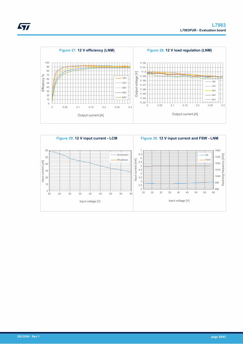
Figure 27. 12 V efficiency (LNM)
0102030405060708090
100
0 0.05 0.1 0.15 0.2 0.25 0.3
Effic
ienc
y %
Output current [A]
18V
24V
36V
48V
60V
Figure 28. 12 V load regulation (LNM)
11.83
11.84
11.85
11.86
11.87
11.88
11.89
11.9
11.91
11.92
0 0.05 0.1 0.15 0.2 0.25 0.3
Out
put v
olta
ge [V
]
Output current [A]
18V
24V
36V
48V
60V
Figure 29. 12 V input current - LCM
0
10
20
30
40
50
60
20 25 30 35 40 45 50 55 60
Inpu
t cur
rent
[uA]
Input voltage [V]
Quiescent
Shutdown
Figure 30. 12 V input current and FSW - LNM
980
990
1000
1010
1020
1030
1040
22.5
33.5
44.5
55.5
66.5
7
20 25 30 35 40 45 50 55 60
Switc
hing
freq
uenc
y [k
Hz]
Inpu
t cur
rent
[mA]
Input voltage [V]
IIN
FSW
L7983L7983PUR - Evaluation board
DS13354 - Rev 1 page 29/43

6.3 L7983PU33R - Evaluation board
In this section the L7983PU33R (VOUT=3.3 V fixed) evaluation board is described.The board schematic is shown in Figure 22 and the PCB layout is depicted in Figure 23 and Figure 24.The main features are:• Programmed VOUT = 3.3 V (fixed)• Max. IOUT = 300 mA• Selected FSW = 1 MHz• VBIAS = VOUT (switch-over enabled)
Table 10. L7983PU33R evaluation board component list (BOM)
Reference Part Package Details Manufacturer P/N
C1 1 μF 1206 X7R/100V/10% TDK C3216X7R2A105K
C2 2.2 μF 0805 X7R/16V/10% TDK C2012X7R1C225K
C3 470 nF 0603 X7R/16V/10%
C4, C5, C10 N.M.
C6 100 nF 0603 X7R/16V/10%
L1 47 μH 4x4 mm 0.56 A sat/ 650 mΩ COILCRAFT LPS4018-473M
R1, R4, R9 0 Ω 0603
R2, R3, R7, R10 N.M.
R5, R6, R8 100 kΩ 0603 1% tolerance
U1 L7983 DFN10_3x3 STM L7983PU33R
Figure 31. 3.3 V fix efficiency (LCM)
0
10
20
30
40
50
60
70
80
90
100
0.0001 0.001 0.01 0.1
Effic
ienc
y %
Output current [A]
12 V
24 V
36 V
48 V
60 V
Figure 32. 3.3 V fix load regulation (LCM)
3.29
3.3
3.31
3.32
3.33
3.34
3.35
3.36
3.37
0 0.05 0.1 0.15 0.2 0.25 0.3
Out
put v
olta
ge [V
]
Output current [A]
12V24V36V48V60V
L7983L7983PU33R - Evaluation board
DS13354 - Rev 1 page 30/43

Figure 33. 3.3 V fix efficiency (LNM)
0102030405060708090
100
0 0.05 0.1 0.15 0.2 0.25 0.3
Effic
ienc
y %
Output current [A]
12V
24V
36V
48V
60V
Figure 34. 3.3 V fix load regulation (LNM)
3.29
3.3
3.31
3.32
3.33
3.34
3.35
0 0.05 0.1 0.15 0.2 0.25 0.3
Out
put v
olta
ge [V
]
Output current [A]
12V
24V
36V
48V
60V
Figure 35. 3.3 V fix input current, no load (LCM)
02468
101214161820
10 15 20 25 30 35 40 45 50 55 60
Inpu
t cur
rent
[µA]
Input voltage [V]
Quiescent
Shutdown
Figure 36. 3.3 V fix input current, no load (LNM)
0
200
400
600
800
1000
1200
1
1.5
2
2.5
3
3.5
4
10 15 20 25 30 35 40 45 50 55 60
Switc
hing
freq
uenc
y [k
Hz]
Inpu
t cur
rent
[mA]
Input voltage [V]
IIN
FSW
L7983L7983PU33R - Evaluation board
DS13354 - Rev 1 page 31/43

6.4 L7983PU50R - Evaluation board
In this section the L7983PU50R (VOUT = 5 V fixed) evaluation board is described.The board schematic is shown in Figure 22 and the PCB layout is depicted in Figure 23 and Figure 24.The main features are:• Programmed VOUT = 5 V (fixed)• Max. IOUT = 300 mA• Selected FSW = 1 MHz• VBIAS = VOUT (switch-over enabled)
Table 11. L7983PU50R evaluation board component list (BOM)
Reference Part Package Details Manufacturer P/N
C1 1 μF 1206 X7R/100V/10% TDK C3216X7R2A105K
C2 2.2 μF 0805 X7R/16V/10% TDK C2012X7R1C225K
C3 470 nF 0603 X7R/16V/10%
C4, C5, C10 N.M.
C6 100 nF 0603 X7R/16V/10%
L1 47 μH 4x4 mm 0.56 A sat/ 650 mΩ COILCRAFT LPS4018-473M
R1, R4, R9 0 Ω 0603
R2, R3, R7, R10 N.M.
R5, R6, R8 100 kΩ 0603 1% tolerance
U1 L7983 DFN10_3x3 STM L7983PU50R
Figure 37. 5 V fix efficiency (LCM)
0
10
20
30
40
50
60
70
80
90
100
0.0001 0.001 0.01 0.1
Effic
ienc
y %
Output current [A]
12 V
24 V
36 V
48 V
60 V
Figure 38. 5 V fix load regulation (LCM)
4.98
5
5.02
5.04
5.06
5.08
5.1
0 0.05 0.1 0.15 0.2 0.25 0.3
Out
put v
olta
ge [V
]
Output current [A]
12V
24V
36V
48V
60V
L7983L7983PU50R - Evaluation board
DS13354 - Rev 1 page 32/43

Figure 39. 5 V fix efficiency (LNM)
0102030405060708090
100
0 0.05 0.1 0.15 0.2 0.25 0.3
Effic
ienc
y %
Output current [A]
12V24V36V48V60V
Figure 40. 5 V fix load regulation (LNM)
4.98
4.99
5
5.01
5.02
5.03
5.04
5.05
5.06
5.07
0 0.05 0.1 0.15 0.2 0.25 0.3
Out
put v
olta
ge [V
]
Output current [A]
12V24V36V48V60V
Figure 41. 5 V fix input current, no load (LCM)
0
5
10
15
20
25
30
35
10 15 20 25 30 35 40 45 50 55 60
Inpu
t cur
rent
[µA]
Input voltage [V]
Quiescent
Shutdown
Figure 42. 5 V fix input current, no load (LNM)
0
200
400
600
800
1000
1200
1
1.5
2
2.5
3
3.5
4
10 15 20 25 30 35 40 45 50 55 60
Switc
hing
freq
uenc
y [k
Hz]
Inpu
t cur
rent
[mA]
Input voltage [V]
IIN
FSW
L7983L7983PU50R - Evaluation board
DS13354 - Rev 1 page 33/43

7 Package information
In order to meet environmental requirements, ST offers these devices in different grades of ECOPACK packages,depending on their level of environmental compliance. ECOPACK specifications, grade definitions and productstatus are available at: www.st.com. ECOPACK is an ST trademark.
L7983Package information
DS13354 - Rev 1 page 34/43

7.1 DFN10 (3 x 3 x 0.8 mm) package information
Figure 43. DFN10 (3 x 3 x 0.8 mm) package outline
BOTTOM VIEW
SIDE VIEW
TOP VIEW
L7983DFN10 (3 x 3 x 0.8 mm) package information
DS13354 - Rev 1 page 35/43

Table 12. DFN10 (3 x 3 x 0.8 mm) mechanical data
SYMBOLDimensions (mm)
Min. Typ. Max.
A 0.70 0.75 0.80
A1 0.0 0.02 0.05
A3 0.20 Ref.
b 0.16 0.23 0.28
D 3.00 BSC
D2 0.27 0.42 0.52
e 0.50 BSC
E 3.0 BSC
E2 0.63 0.78 0.88
L 0.30 0.40 0.50
K 0.20
N 10
NE 5
Figure 44. DFN10 (3 x 3 x 0.8 mm) recommended footprint
L7983DFN10 (3 x 3 x 0.8 mm) package information
DS13354 - Rev 1 page 36/43

8 Ordering information
Table 13. Order codes
Part numbers Output voltage Package Packaging
L7983PUR Adjustable
DFN10 Tape and reelL7983PU33R Fixed 3.3 V
L7983PU50R Fixed 5.0 V
L7983Ordering information
DS13354 - Rev 1 page 37/43

Revision history
Table 14. Document revision history
Date Revision Changes
01-Oct-2020 1 Initial release.
L7983
DS13354 - Rev 1 page 38/43

Contents
1 Application schematic and block diagram. . . . . . . . . . . . . . . . . . . . . . . . . . . . . . . . . . . . . . . . . .3
1.1 Application circuit . . . . . . . . . . . . . . . . . . . . . . . . . . . . . . . . . . . . . . . . . . . . . . . . . . . . . . . . . . . . . . 3
2 Pin settings. . . . . . . . . . . . . . . . . . . . . . . . . . . . . . . . . . . . . . . . . . . . . . . . . . . . . . . . . . . . . . . . . . . . . . . .4
3 Absolute maximum ratings . . . . . . . . . . . . . . . . . . . . . . . . . . . . . . . . . . . . . . . . . . . . . . . . . . . . . . . .5
3.1 Thermal characteristics . . . . . . . . . . . . . . . . . . . . . . . . . . . . . . . . . . . . . . . . . . . . . . . . . . . . . . . . . 5
3.2 ESD protection . . . . . . . . . . . . . . . . . . . . . . . . . . . . . . . . . . . . . . . . . . . . . . . . . . . . . . . . . . . . . . . . 5
3.3 Operating conditions. . . . . . . . . . . . . . . . . . . . . . . . . . . . . . . . . . . . . . . . . . . . . . . . . . . . . . . . . . . . 6
4 Electrical characteristics. . . . . . . . . . . . . . . . . . . . . . . . . . . . . . . . . . . . . . . . . . . . . . . . . . . . . . . . . . .7
5 Functional description . . . . . . . . . . . . . . . . . . . . . . . . . . . . . . . . . . . . . . . . . . . . . . . . . . . . . . . . . . . . .9
5.1 Power section . . . . . . . . . . . . . . . . . . . . . . . . . . . . . . . . . . . . . . . . . . . . . . . . . . . . . . . . . . . . . . . . . 9
5.2 Control loop and voltage programming . . . . . . . . . . . . . . . . . . . . . . . . . . . . . . . . . . . . . . . . . . . . 9
5.2.1 LNM/LCM selection and synchronization . . . . . . . . . . . . . . . . . . . . . . . . . . . . . . . . . . . . . 12
5.3 Switching frequency programming and dithering . . . . . . . . . . . . . . . . . . . . . . . . . . . . . . . . . . . 15
5.4 Enable and Reset . . . . . . . . . . . . . . . . . . . . . . . . . . . . . . . . . . . . . . . . . . . . . . . . . . . . . . . . . . . . . 17
5.5 VCC and switchover . . . . . . . . . . . . . . . . . . . . . . . . . . . . . . . . . . . . . . . . . . . . . . . . . . . . . . . . . . . 19
5.6 Fault management . . . . . . . . . . . . . . . . . . . . . . . . . . . . . . . . . . . . . . . . . . . . . . . . . . . . . . . . . . . . 19
5.6.1 Overcurrent protection (OCP) . . . . . . . . . . . . . . . . . . . . . . . . . . . . . . . . . . . . . . . . . . . . . . 20
5.6.2 Overvoltage protection (OVP) . . . . . . . . . . . . . . . . . . . . . . . . . . . . . . . . . . . . . . . . . . . . . . 22
5.6.3 Overtemperature protection (OTP) . . . . . . . . . . . . . . . . . . . . . . . . . . . . . . . . . . . . . . . . . . 22
5.7 Application design guidelines . . . . . . . . . . . . . . . . . . . . . . . . . . . . . . . . . . . . . . . . . . . . . . . . . . . 23
5.7.1 Input capacitor selection . . . . . . . . . . . . . . . . . . . . . . . . . . . . . . . . . . . . . . . . . . . . . . . . . . 23
5.7.2 Inductor selection . . . . . . . . . . . . . . . . . . . . . . . . . . . . . . . . . . . . . . . . . . . . . . . . . . . . . . . 23
5.7.3 Output capacitor selection. . . . . . . . . . . . . . . . . . . . . . . . . . . . . . . . . . . . . . . . . . . . . . . . . 23
5.7.4 Layout considerations . . . . . . . . . . . . . . . . . . . . . . . . . . . . . . . . . . . . . . . . . . . . . . . . . . . . 24
5.7.5 Thermal considerations. . . . . . . . . . . . . . . . . . . . . . . . . . . . . . . . . . . . . . . . . . . . . . . . . . . 25
6 Evaluation board . . . . . . . . . . . . . . . . . . . . . . . . . . . . . . . . . . . . . . . . . . . . . . . . . . . . . . . . . . . . . . . . .26
6.1 Schematic and PCB layout . . . . . . . . . . . . . . . . . . . . . . . . . . . . . . . . . . . . . . . . . . . . . . . . . . . . . 26
6.2 L7983PUR - Evaluation board . . . . . . . . . . . . . . . . . . . . . . . . . . . . . . . . . . . . . . . . . . . . . . . . . . . 28
6.3 L7983PU33R - Evaluation board. . . . . . . . . . . . . . . . . . . . . . . . . . . . . . . . . . . . . . . . . . . . . . . . . 30
L7983Contents
DS13354 - Rev 1 page 39/43

6.4 L7983PU50R - Evaluation board. . . . . . . . . . . . . . . . . . . . . . . . . . . . . . . . . . . . . . . . . . . . . . . . . 32
7 Package information. . . . . . . . . . . . . . . . . . . . . . . . . . . . . . . . . . . . . . . . . . . . . . . . . . . . . . . . . . . . . .34
7.1 DFN10 (3x3) package information . . . . . . . . . . . . . . . . . . . . . . . . . . . . . . . . . . . . . . . . . . . . . . . 35
8 Ordering information . . . . . . . . . . . . . . . . . . . . . . . . . . . . . . . . . . . . . . . . . . . . . . . . . . . . . . . . . . . . .37
Revision history . . . . . . . . . . . . . . . . . . . . . . . . . . . . . . . . . . . . . . . . . . . . . . . . . . . . . . . . . . . . . . . . . . . . . . .38
L7983Contents
DS13354 - Rev 1 page 40/43
List of tablesTable 1. Pin description. . . . . . . . . . . . . . . . . . . . . . . . . . . . . . . . . . . . . . . . . . . . . . . . . . . . . . . . . . . . . . . . . . . . . . 4Table 2. Absolute maximum ratings . . . . . . . . . . . . . . . . . . . . . . . . . . . . . . . . . . . . . . . . . . . . . . . . . . . . . . . . . . . . . 5Table 3. Thermal data. . . . . . . . . . . . . . . . . . . . . . . . . . . . . . . . . . . . . . . . . . . . . . . . . . . . . . . . . . . . . . . . . . . . . . . 5Table 4. ESD performance . . . . . . . . . . . . . . . . . . . . . . . . . . . . . . . . . . . . . . . . . . . . . . . . . . . . . . . . . . . . . . . . . . . 5Table 5. Recommended operating conditions. . . . . . . . . . . . . . . . . . . . . . . . . . . . . . . . . . . . . . . . . . . . . . . . . . . . . . . 6Table 6. Electrical characteristics . . . . . . . . . . . . . . . . . . . . . . . . . . . . . . . . . . . . . . . . . . . . . . . . . . . . . . . . . . . . . . . 7Table 7. FSW pin programming resistor . . . . . . . . . . . . . . . . . . . . . . . . . . . . . . . . . . . . . . . . . . . . . . . . . . . . . . . . . 15Table 8. Reference applications – VIN = 24 V, CIN = 1 µF, CVCC = 470 nF. . . . . . . . . . . . . . . . . . . . . . . . . . . . . . . . . . 24Table 9. L7983PUR evaluation board component list (BOM) . . . . . . . . . . . . . . . . . . . . . . . . . . . . . . . . . . . . . . . . . . . 28Table 10. L7983PU33R evaluation board component list (BOM) . . . . . . . . . . . . . . . . . . . . . . . . . . . . . . . . . . . . . . . . . 30Table 11. L7983PU50R evaluation board component list (BOM) . . . . . . . . . . . . . . . . . . . . . . . . . . . . . . . . . . . . . . . . . 32Table 12. DFN10 (3 x 3 x 0.8 mm) mechanical data . . . . . . . . . . . . . . . . . . . . . . . . . . . . . . . . . . . . . . . . . . . . . . . . . . 36Table 13. Order codes . . . . . . . . . . . . . . . . . . . . . . . . . . . . . . . . . . . . . . . . . . . . . . . . . . . . . . . . . . . . . . . . . . . . . . 37Table 14. Document revision history . . . . . . . . . . . . . . . . . . . . . . . . . . . . . . . . . . . . . . . . . . . . . . . . . . . . . . . . . . . . . 38
L7983List of tables
DS13354 - Rev 1 page 41/43
List of figuresFigure 1. Typical application circuit . . . . . . . . . . . . . . . . . . . . . . . . . . . . . . . . . . . . . . . . . . . . . . . . . . . . . . . . . . . . . 3Figure 2. Block diagram . . . . . . . . . . . . . . . . . . . . . . . . . . . . . . . . . . . . . . . . . . . . . . . . . . . . . . . . . . . . . . . . . . . . 3Figure 3. Pin connection (top view) . . . . . . . . . . . . . . . . . . . . . . . . . . . . . . . . . . . . . . . . . . . . . . . . . . . . . . . . . . . . . 4Figure 4. Control loop block diagram. . . . . . . . . . . . . . . . . . . . . . . . . . . . . . . . . . . . . . . . . . . . . . . . . . . . . . . . . . . 10Figure 5. Output voltage programming - adjustable version . . . . . . . . . . . . . . . . . . . . . . . . . . . . . . . . . . . . . . . . . . . 11Figure 6. Output voltage programming - fixed version . . . . . . . . . . . . . . . . . . . . . . . . . . . . . . . . . . . . . . . . . . . . . . . 11Figure 7. LNM selected, no load . . . . . . . . . . . . . . . . . . . . . . . . . . . . . . . . . . . . . . . . . . . . . . . . . . . . . . . . . . . . . . 12Figure 8. LCM selected, no load . . . . . . . . . . . . . . . . . . . . . . . . . . . . . . . . . . . . . . . . . . . . . . . . . . . . . . . . . . . . . . 13Figure 9. LCM selected, 10 mA load . . . . . . . . . . . . . . . . . . . . . . . . . . . . . . . . . . . . . . . . . . . . . . . . . . . . . . . . . . . 13Figure 10. LCM selected, 50 mA load . . . . . . . . . . . . . . . . . . . . . . . . . . . . . . . . . . . . . . . . . . . . . . . . . . . . . . . . . . . 14Figure 11. LCM to LNM transition, no load. . . . . . . . . . . . . . . . . . . . . . . . . . . . . . . . . . . . . . . . . . . . . . . . . . . . . . . . 14Figure 12. RVCC = 0 Ω, dithering enabled, no load. . . . . . . . . . . . . . . . . . . . . . . . . . . . . . . . . . . . . . . . . . . . . . . . . . 16Figure 13. RVCC = 0 Ω, dithering enabled, no load. Detail. . . . . . . . . . . . . . . . . . . . . . . . . . . . . . . . . . . . . . . . . . . . . 16Figure 14. Turn-on example. . . . . . . . . . . . . . . . . . . . . . . . . . . . . . . . . . . . . . . . . . . . . . . . . . . . . . . . . . . . . . . . . . 17Figure 15. Turn-off example. . . . . . . . . . . . . . . . . . . . . . . . . . . . . . . . . . . . . . . . . . . . . . . . . . . . . . . . . . . . . . . . . . 18Figure 16. Input voltage turn-on threshold programming . . . . . . . . . . . . . . . . . . . . . . . . . . . . . . . . . . . . . . . . . . . . . . 18Figure 17. Output voltage and RST behavior . . . . . . . . . . . . . . . . . . . . . . . . . . . . . . . . . . . . . . . . . . . . . . . . . . . . . . 19Figure 18. Peak current limit . . . . . . . . . . . . . . . . . . . . . . . . . . . . . . . . . . . . . . . . . . . . . . . . . . . . . . . . . . . . . . . . . 20Figure 19. Valley current limit . . . . . . . . . . . . . . . . . . . . . . . . . . . . . . . . . . . . . . . . . . . . . . . . . . . . . . . . . . . . . . . . . 20Figure 20. Negative current limit example . . . . . . . . . . . . . . . . . . . . . . . . . . . . . . . . . . . . . . . . . . . . . . . . . . . . . . . . 21Figure 21. Overvoltage protection. . . . . . . . . . . . . . . . . . . . . . . . . . . . . . . . . . . . . . . . . . . . . . . . . . . . . . . . . . . . . . 22Figure 22. Evaluation board schematic . . . . . . . . . . . . . . . . . . . . . . . . . . . . . . . . . . . . . . . . . . . . . . . . . . . . . . . . . . 26Figure 23. PCB layout (Top). . . . . . . . . . . . . . . . . . . . . . . . . . . . . . . . . . . . . . . . . . . . . . . . . . . . . . . . . . . . . . . . . . 27Figure 24. PCB layout (Bottom) . . . . . . . . . . . . . . . . . . . . . . . . . . . . . . . . . . . . . . . . . . . . . . . . . . . . . . . . . . . . . . . 27Figure 25. 12 V efficiency (LCM) . . . . . . . . . . . . . . . . . . . . . . . . . . . . . . . . . . . . . . . . . . . . . . . . . . . . . . . . . . . . . . 28Figure 26. 12 V load regulation (LCM). . . . . . . . . . . . . . . . . . . . . . . . . . . . . . . . . . . . . . . . . . . . . . . . . . . . . . . . . . . 28Figure 27. 12 V efficiency (LNM) . . . . . . . . . . . . . . . . . . . . . . . . . . . . . . . . . . . . . . . . . . . . . . . . . . . . . . . . . . . . . . 29Figure 28. 12 V load regulation (LNM). . . . . . . . . . . . . . . . . . . . . . . . . . . . . . . . . . . . . . . . . . . . . . . . . . . . . . . . . . . 29Figure 29. 12 V input current - LCM . . . . . . . . . . . . . . . . . . . . . . . . . . . . . . . . . . . . . . . . . . . . . . . . . . . . . . . . . . . . 29Figure 30. 12 V input current and FSW - LNM . . . . . . . . . . . . . . . . . . . . . . . . . . . . . . . . . . . . . . . . . . . . . . . . . . . . . 29Figure 31. 3.3 V fix efficiency (LCM) . . . . . . . . . . . . . . . . . . . . . . . . . . . . . . . . . . . . . . . . . . . . . . . . . . . . . . . . . . . . 30Figure 32. 3.3 V fix load regulation (LCM) . . . . . . . . . . . . . . . . . . . . . . . . . . . . . . . . . . . . . . . . . . . . . . . . . . . . . . . . 30Figure 33. 3.3 V fix efficiency (LNM) . . . . . . . . . . . . . . . . . . . . . . . . . . . . . . . . . . . . . . . . . . . . . . . . . . . . . . . . . . . . 31Figure 34. 3.3 V fix load regulation (LNM) . . . . . . . . . . . . . . . . . . . . . . . . . . . . . . . . . . . . . . . . . . . . . . . . . . . . . . . . 31Figure 35. 3.3 V fix input current, no load (LCM). . . . . . . . . . . . . . . . . . . . . . . . . . . . . . . . . . . . . . . . . . . . . . . . . . . . 31Figure 36. 3.3 V fix input current, no load (LNM). . . . . . . . . . . . . . . . . . . . . . . . . . . . . . . . . . . . . . . . . . . . . . . . . . . . 31Figure 37. 5 V fix efficiency (LCM) . . . . . . . . . . . . . . . . . . . . . . . . . . . . . . . . . . . . . . . . . . . . . . . . . . . . . . . . . . . . . 32Figure 38. 5 V fix load regulation (LCM) . . . . . . . . . . . . . . . . . . . . . . . . . . . . . . . . . . . . . . . . . . . . . . . . . . . . . . . . . 32Figure 39. 5 V fix efficiency (LNM) . . . . . . . . . . . . . . . . . . . . . . . . . . . . . . . . . . . . . . . . . . . . . . . . . . . . . . . . . . . . . 33Figure 40. 5 V fix load regulation (LNM) . . . . . . . . . . . . . . . . . . . . . . . . . . . . . . . . . . . . . . . . . . . . . . . . . . . . . . . . . 33Figure 41. 5 V fix input current, no load (LCM) . . . . . . . . . . . . . . . . . . . . . . . . . . . . . . . . . . . . . . . . . . . . . . . . . . . . . 33Figure 42. 5 V fix input current, no load (LNM) . . . . . . . . . . . . . . . . . . . . . . . . . . . . . . . . . . . . . . . . . . . . . . . . . . . . . 33Figure 43. DFN10 (3 x 3 x 0.8 mm) package outline . . . . . . . . . . . . . . . . . . . . . . . . . . . . . . . . . . . . . . . . . . . . . . . . . 35Figure 44. DFN10 (3 x 3 x 0.8 mm) recommended footprint . . . . . . . . . . . . . . . . . . . . . . . . . . . . . . . . . . . . . . . . . . . . 36
L7983List of figures
DS13354 - Rev 1 page 42/43

IMPORTANT NOTICE – PLEASE READ CAREFULLY
STMicroelectronics NV and its subsidiaries (“ST”) reserve the right to make changes, corrections, enhancements, modifications, and improvements to STproducts and/or to this document at any time without notice. Purchasers should obtain the latest relevant information on ST products before placing orders. STproducts are sold pursuant to ST’s terms and conditions of sale in place at the time of order acknowledgement.
Purchasers are solely responsible for the choice, selection, and use of ST products and ST assumes no liability for application assistance or the design ofPurchasers’ products.
No license, express or implied, to any intellectual property right is granted by ST herein.
Resale of ST products with provisions different from the information set forth herein shall void any warranty granted by ST for such product.
ST and the ST logo are trademarks of ST. For additional information about ST trademarks, please refer to www.st.com/trademarks. All other product or servicenames are the property of their respective owners.
Information in this document supersedes and replaces information previously supplied in any prior versions of this document.
© 2020 STMicroelectronics – All rights reserved
L7983
DS13354 - Rev 1 page 43/43