datasheet - international rectifier
TRANSCRIPT

www.irf.com 1
HIGH RELIABILITYRADIATION HARDENEDLOW POWERDC-DC CONVERTER
ML1000605D
Description
Total Dose > 100 krad(Si)
SEE > 82 MeV.cm2/mg Low Weight < 50 grams 97V to 103V DC Input Range O/P 1: +6.0V (up to 500mA) O/P 2: -5.0V (up to 100mA) Output Ripple: < 1mVrms (100Hz - 50MHz) CS Rejection Input to Outputs: > 90dB (50Hz - 1.0MHz) 10MΩ @ 100VDC Isolation Input Under-Voltage Protection Meets Conducted Emission Requirements of Major Power Buses: 100Hz - 100kHz: 80dBuArms 100kHz - 10MHz: -20dB/decade 10MHz - 50MHz: 40dBuArms Short Circuit and Overload Protection Meets Derating Requirements of EEE-INST 002 and ECSS-Q-30-11A Isolated On/Off Control via High Level Pulse Command (Latching Relay) Status Telemetry (Relay Contact Type) Workmanship Per IPC-A610 Class 3 Board is Coated with ARATHANE-5750
Features
100V Input, Dual Output
Applications
The ML-Series of isolated DC-DC converters for spaceapplications are low power radiation hardened highreliability devices designed for hostile radiationenvironments such as those encountered by geostationaryearth orbit satellites, deep space probes and communicationsystems. Features include small size, high efficiency,low weight, and a good tolerance to total ionizing dose,single event effects, and environmental stresses suchas temperature extremes, mechanical shock, andvibration. All components are fully derated to meet therequirements of EEE-INST-002 (NASA) and ECSS-Q-30-11A (ESA). Extensive documentation including worstcase analysis, radiation susceptibility, thermal analysis,stress analysis, and reliability analysis are available.
The ML-Series converter has two outputs – one positiveand one negative - each is independently regulated vialinear post regulators. The outputs are sequencedduring turn-on and turn-off such that negative outputcomes up first at turn-on and stays up at turn-off until thepositive output has decreased. The ML-series convertersincorporate a fixed frequency flyback power converterand internal EMI filter that meets the requirements formost major satellite power buses. The converter includesisolated On/Off telecommand with associated statustelemetry. The converter also includes input undervoltage shut-down functionality.
Due to the linear post regulation of the outputs, the ML-Series is well suited for use in RF-applications wherelow noise, high output voltage accuracy, and high CSattenuation is required.
Each converter is provided as a complete boardassembly for installation into the host equipment chassis.The board is conformal coated (except for matingsurfaces) and is mounted in the host chassis usingscrews. The board outline is L x W x H: 70mm x 50mm x18mm. The weight is less than 50 grams.
Low Power RF Systems (like LNA) on-boardSatellites
Non-flight versions of the ML-Series convertersare available for system development purposes.Variations in electrical specifications andscreening to meet custom requirements can beaccommodated.
PD-97806
2 www.irf.com
ML1000605D(100V Input, Dual Output)
Circuit Description
An under-voltage protection circuit prohibits theconverter from operating when the line voltage istoo low for safe operation. In case of an undervoltage event the converter will not start when theinput voltage returns to its nominal level before anOff-command followed by an On-command has beenissued.
The isolated On/Off telecommand is made with alatching relay and is intended for use with a 26Vpulse command. A status telemetry derived from aspare set of contacts in the relay is used for statustelemetry.
Design MethodologyThe ML-Series is developed using a provenconservative design methodology, which includesselecting radiation tolerant, and establishedreliability components and full derating to the
requirements of EEE-INST-002 and ECSS-ST-11A.
The ML-Series converters utilize two-stage regulationwith a flyback topology with a switching frequency of140kHz for primary regulation and linear postregulation for each of the outputs.
The Output power is limited under any load faultcondition to approximately 120% of rated output.An overload condition on the positive output causesthe converter output to behave like a constant currentsource with the output voltage dropping belownominal. An overload condition at the negative outputcauses the positive output to shut-down in order toprotect RF-transistors in the load. The converter willresume normal operation when the load current isreduced below the current limit point.
For further information please refer to the ML-Seriesgeneric description available at www.irf.com.

www.irf.com 3
ML1000605D (100V Input, Dual Output)
Electrical Performance Characteristics
For Notes to Specifications, refer to page 5
Specifications
* Meets full derating
Input voltage range -0.5Vdc to +120Vdc Input voltage range (Note 9) +97Vdc to +103Vdc
Output power Internally limited Output power 0 to Max. Rated
Operating mounting point -55°C to +100°C Operating mounting point -40°C to +75°C *
temperature (Note 10) temperature (Note 9)
Storage temperature -55°C to +125°C Cold start temperature -55°C
Recommended Operating Conditions Absolute Maximum Ratings
Limits
Parameter Condition
Conditions
-40°C ≤ Tc ≤ +75°C
VIN = 100V DC ± 0.5%, CL = 0µF
unless otherwise specified
Min Nom Max Unit
Primary Input Voltage 97 100 103 V
Output voltage ( VOUT )
(O/P 1, O/P 2)
+6.0V
-5.0V
+6.0V
-5.0V
+6.0V
-5.0V
1
1
2
2
3
3
Note 1
0% ≤ IOUT ≤ 100% of rated load
0% ≤ IOUT ≤ 100% of rated load
0% ≤ IOUT ≤ 100% of rated load
+5.970
-4.975
+5.940
-4.950
+5.880
-4.900
+6.00
-5.00
+6.030
-5.025
+6.060
-5.050
6.120
5.100
V
V
V
Output power ( POUT )
(O/P 1, O/P 2)
+6.0V
-5.0V
1,2,3
VIN = 97, 100, 103V
3.0
0.5
W
Output current ( IOUT )
(O/P 1, O/P 2)
+6.0V
-5.0V
1,2,3
VIN = 97, 100, 103V
0
0
500
100
mA
Line regulation ( VRLINE )
Each output
1,2,3 VIN = 97, 100, 103V
IOUT = 10%, 50%, 100% rated
-1.0
1.0
mV
Load regulation ( VRLOAD )
Each output
1,2,3 IOUT = 10%, 50%, 100% rated
VIN = 97, 100, 103V
-1.0
1.0
mV
Cross regulation ( VRCROSS )
1,2,3
VIN = 97, 100, 103V, Note 1
1.0
mV
Input current
1,2,3 IOUT = 0, commanded On
Commanded Off
10 15
2.0
mA
Switching frequency ( FS ) 1,2,3 Notes 1, 7 126 140 154 kHz
Input under voltage
Trig level
1,2,3
0% ≤ IOUT ≤ 100% of rated load
85
95
V
Output Sequencing
Turn-on delay O/P 2 to O/P 1
Turn-off delay O/P1 to O/P 2
1,2,3
IOUT ≥ 20% for Output 1
2.0
1.0
12
8.0
ms
4 www.irf.com
ML1000605D(100V Input, Dual Output)
Electrical Performance Characteristics (continued)
For Notes to Specifications, refer to page 5
Limits
Parameter Condition
Conditions
-40°C ≤ Tc ≤ +75°C
VIN = 100V DC ± 0.5%, CL = 0µF
unless otherwise specified Min Nom Max
Unit
Output ripple ( VRIP )
Each output
+6.0V
-5.0V
+6.0V
-5.0V
1
1,2
VIN = 97, 100, 103V
IOUT = 100% rated load
Frequency domain 100Hz – 50MHz
Note 1
Time domain 100Hz – 50MHz
Notes 1, 2
1.0
1.0
30
30
mVrms
mVpp
Efficiency ( EFF )
For combined output power
of
0.70W
1.75W
3.50W
1,2,3
IOUT = 20% rated load
IOUT = 50% rated load
IOUT = 100% rated load
37
52
60
38
54
62
%
Telecommand I/F
Pulse Voltage high
Pulse Voltage low
Pulse duration
1,2,3
Note 1
+22
-40
10
+30
0.5
1000
V
V
ms
Telemetry
Converter On
Converter Off
1,2,3
400
1.0
422
450
ohm
Mohm
Current Limit Point
Each output
+6.0V
-5.0V
1,2,3
VOUT = 100mV below Nominal
550
110
700
150
mA
Output response to step load changes ( VTLD )
+6.0V
-5.0V
1,2,3
20% to / from 100% Load, Note 3
-70
-50
70
50
mV pk
Recovery time,
step load changes ( TTLD )
+6.0
-5.0
1,2,3
20% to / from 100% Load , Notes 3, 4
2.5
2.5
ms
Turn-on Response
Overshoot ( VOS )
+6.0V
-5.0V
Turn-on Delay
1,2,3
10% Load, Full Load
Note 5
2.0
60
50
10
mV
ms
Capacitive Load ( CL )
+6.0V
-5.0V
1
IOUT = 100% rated load
No effect on DC performance
Notes 1, 6
Each output
100
100
µF
www.irf.com 5
ML1000605D (100V Input, Dual Output)
Electrical Performance Characteristics (continued)
Notes: Specification and Electrical Performance Characteristics Tables
1. Parameter is tested as part of design characterization or after design changes. Thereafter, parameter shallbe guaranteed to the limits specified.
2. Guaranteed for a D.C. to 50MHz bandwidth. Tested using a 10.7MHz bandwidth.3. Load current step transition time ≥ 10 µs.4. Recovery time is measured from the initiation of the transient to where VOUT has returned to within ±1% of
its steady state value.5. Turn-on delay time from application of telecommand pulse to the point where Output 2 = 98% of nominal
output voltage.6. Capacitive load may be any value from 0 to the maximum limit without compromising the output sequencing
performance. A capacitive load in excess of the maximum limit may influence the output sequencingperformance and start-up time, converter operation and dc performance will remain intact.
7. The switching frequency and 1st and 2nd harmonic of the input ripple is tested on every unit.8. MIL-HDBK-217F2 stress-dependent method is used with 2 exceptions: For soldering a fixed failure rate at
0.035FIT is used and for power MOSFETs the dissipated power (instead of rated power) is used for the Prparameter. 1 FIT is 1 failure in 109 hours.
9. The converter meets full derating per EEE-INST-002 and ECSS-Q-30-11A with the following exception: ForSchottky diode JANS1N5819 a maximum derated junction temperature of +110°C. For EEE-INST-002 it isrequired that ceramic capacitors with a voltage stress below 10V shall be rated for minimum 100V - in theproduct such capacitors is rated for 50V minimum.
10. Although operation temperatures between -55°C to +100°C and -40°C to+75°C is guaranteed, no parameter limits are specified.
Electrical Performance Characteristics - Definition of Conditions
Condition Definition Comment1 BOL @ +25°C interface temperature Initial setting
2 BOL @ -40°C to +75°C interface temperature Initial setting and worst case temperature variation
3 EOL @ -40°C to +75°C interface temperature Worst case performance including initial setting, temperature variation, aging and radiation degradation
Limits
Parameter Condition
Conditions -40°C ≤ Tc ≤ +75°C
VIN = 100V DC ± 0.5%, CL = 0µF unless otherwise specified
Min Nom Max Unit
EMC conducted
susceptibility
(Line rejection)
1 IOUT = 100% rated load
Primary power sine wave injection of 2Vp-p, 100Hz to 1MHz, Note 1
96
110
dB
Electromagnetic Interference (EMI), conducted emission (CE)
1 IOUT = 100% rated load, Notes 1, 7
Limits per Figures 4 and 5
Isolation 1 Input to Output, any potential to telecommand input and any potential to
telemetry output, test @ 100VDC
10
MΩ
Device Weight 50 g
Failure Rate MIL-HDBK-217F2, SF, 35°C, Note 8 60 FITs

6 www.irf.com
ML1000605D(100V Input, Dual Output)
Model Definition and Test Plans
Model Description Build Standard
EBB The EBB is an electrical representative model.
The EBB is intended to be used by customers in their proto type at equipment level.
EBB models are built at IR’s Danish Design Center.
The PCB will be hand soldered by the engineering group. No staking and conformal coating is foreseen
Preferably same type of EEE parts as intended for flight, but lower grade will be used for convenience. For resistors and capacitors different types with same basic characteristics may be used
EQM The EQM is an electrical and mechanical representative model.
The EQM is intended to be used by customer in their EQM at equipment level.
Flight standard for processes.
Same type of EEE parts as intended for flight, but lower grade may be used for convenience.
FM Flight standard models. Full flight standard
Model Definition
Test Plan - A
The EBB must pass the following tests:
Test No. Type of Test Location* Remarks
1 Electrical performance test, room temperature incl. Limited EMC test (CE 50kHz-1MHz)
IRD
Acceptance Test Procedure
2 Electrical performance test in temperature (Q-level)
IRD Acceptance Test Procedure
3 Electrical performance test, room temperature incl. Limited EMC test (CE 50kHz-1MHz)
IRD Acceptance Test Procedure
4 Final Inspection IRD General inspection Procedure
www.irf.com 7
ML1000605D (100V Input, Dual Output)
Test Plan - B
Test Plan - C
Note:Location* - IRD: IR’s Danish Design Center, Skovlunde, Denmark - IRSJ: IR’s Site in San Jose, California, USA
The EQM must pass the following tests:
Test No. Type of Test Location* Remarks
1 Electrical performance test, room temperature incl. Limited EMC test (CE 50kHz-1MHz)
IRSJ Acceptance Test Procedure
2 Thermal cycling with electrical monitoring of input and outputs (Q-level)
IRSJ Acceptance Test Procedure
10 cycles
3 Electrical performance test in temperature (Q-level)
IRSJ Acceptance Test Procedure
4 Random Vibration test in (Q-level)
External test house
Vibration Test Procedure
5 Electrical performance test, room temperature incl. Limited EMC test (CE 50kHz-1MHz)
IRSJ Acceptance Test Procedure
6 Mechanical Measurements IRSJ Acceptance Test Procedure
7 Final Inspection IRSJ General inspection Procedure
The FM must pass the following tests:
Test No. Type of Test Location* Remarks
1 Electrical performance test, room temperature incl. Limited EMC test (CE 50kHz-1MHz)
IRSJ Acceptance test procedure
2 Electrical performance test in temperature (A-levels)
IRSJ Acceptance test procedure
3 Electrical performance test, room temperature incl. Limited EMC test (CE 50kHz-1MHz)
IRSJ Acceptance test procedure
4 Electrical performance test, room temperature
IRSJ Acceptance Test Procedure
5 Mechanical Measurements IRSJ Acceptance test procedure
6 Final Inspection IRSJ General inspection procedure
8 www.irf.com
ML1000605D(100V Input, Dual Output)
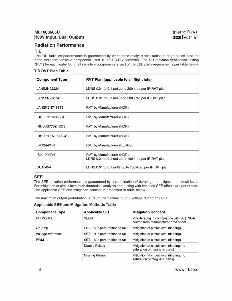
Radiation PerformanceTIDThe TID radiation performance is guaranteed by worst case analysis with radiation degradation data foreach radiation sensitive component used in the DC-DC converter. For TID radiation verification testing(RVT) for each wafer lot for all sensitive components is part of the EEE parts requirements per table below.
Component Type RVT Plan (applicable to all flight lots)
JANS2N2222A LDRS 0.01 to 0.1 rad up to 200 krad per IR RVT plan
JANS2N2907A LDRS 0.01 to 0.1 rad up to 200 krad per IR RVT plan
JANSR2N7492T2 RVT by Manufacturer (HDR)
IRHF57214SESCS RVT by Manufacturer (HDR)
IRHLUB770Z4SCS RVT by Manufacturer (HDR)
IRHLUB7970Z4SCS RVT by Manufacturer (HDR)
LM124AWR RVT by Manufacturer (ELDRS)
IS2-1009RH RVT by Manufacturer (HDR) LDRS 0.01 to 0.1 rad up to 100 krad per IR RVT plan
UC1845A LDRS 0.01 to 0.1 rad/s up to 100kRad per IR RVT plan
TID RVT Plan Table
SEEThe SEE radiation performance is guaranteed by a combination of derating and mitigation at circuit level.For mitigation at circuit level both theoretical analysis and testing with imposed SEE effects are performed.The applicable SEE and mitigation concept is presented in table below.
The maximum output perturbation is 5% of the nominal output voltage during any SEE.
Component Type Applicable SEE Mitigation Concept
RH MOSFET SEGR Vds derating in combination with SEE SOA curves from manufacturer data sheet
Op-Amp SET, 15us perturbation to rail Mitigation at circuit level (filtering)
Voltage reference SET, 10us perturbation to rail Mitigation at circuit level (filtering)
SET, 15us perturbation to rail Mitigation at circuit level (filtering)
Double Pulses Mitigation at circuit level (filtering, no saturation of magnetic parts)
PWM
Missing Pulses Mitigation at circuit level (filtering, no saturation of magnetic parts)
Applicable SEE and Mitigation Methods Table

www.irf.com 9
ML1000605D (100V Input, Dual Output)
EEE Parts Technical StandardFor component screening and DPA rules, refer to the generic ML-Series data sheet at www.irf.com.
Random Vibration
Fig 1- Block Diagram
Grounding and Isolation Scheme
Axis Frequency Range (Hz) Level PSD Level (grms) Duration (S)
20-100 +6 dB/oct
100-1600 0.5 SQR(g)/Hz X, Y, Z
1600-2000 -12 dB/oct
29.9 180
Parameter Grounding & Isolation Performance
Isolation:
Primary to Secondary:
Telecommand:
Status TM:
> 10 MOhm // < 50nF
Floating
Floating
Grounding: Secondary return bound to chassis via multiple screw connections
Input Filter
Fly-BackTrans-former
Rectifier & Filter
Rectifier&
Filter
Linear Regulator
Rectifier&
Filter
Fly-BackPower Switch
PWM Controller
UVP Monitor &
Latch
Latching Relay
Current Shunt
Start-UpResistor
Negative Linear
Regulator
Primary Power Bus
TC ON
TC OFF
on/off TM
Disable
Int.SupplyV1: +6V 500mA
V2: -5V 100mA
Rectifier&
FilterInternalaux
Output Sequencing
10 www.irf.com
ML1000605D(100V Input, Dual Output)
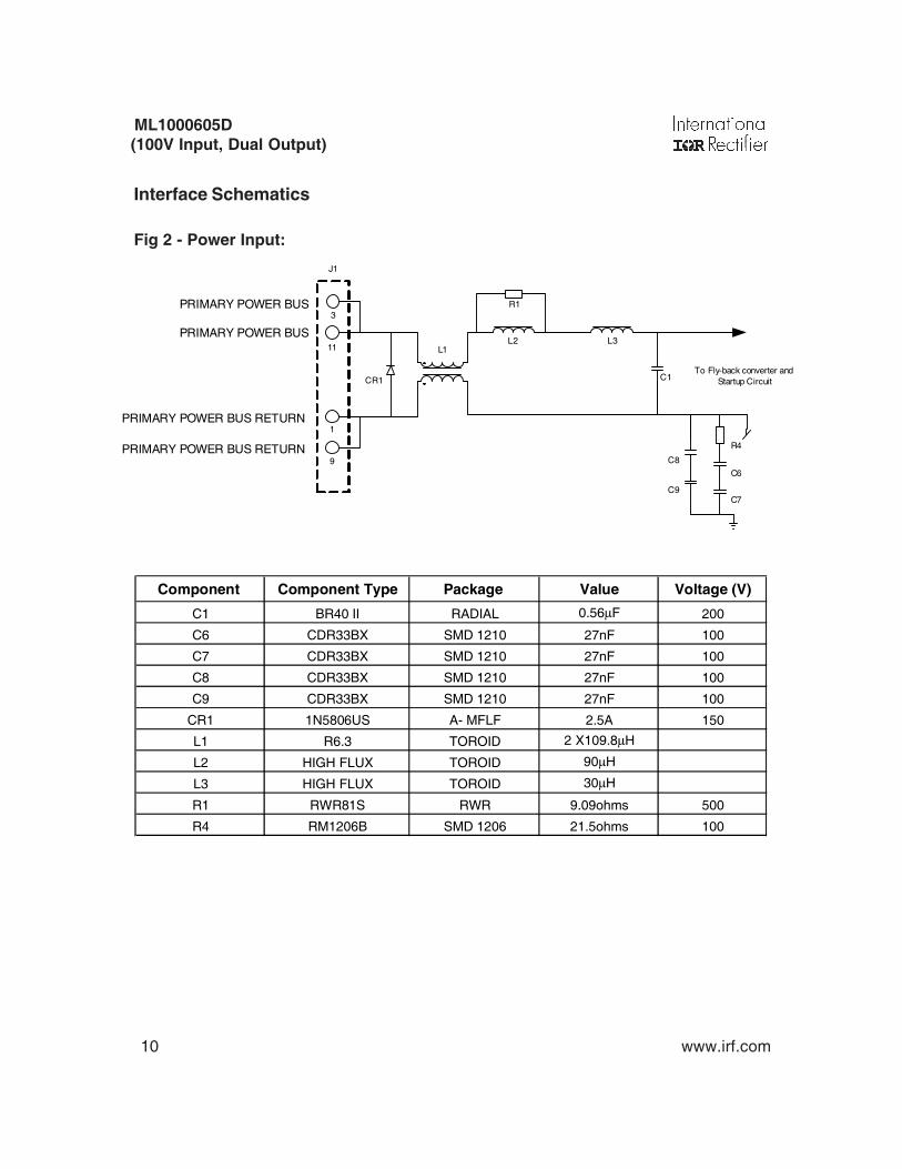
Interface Schematics
Fig 2 - Power Input:
L1L3L2
R1
C1
C8
C6
R4
PRIMARY POWER BUS
J1
3
1
C9C7
11
9
PRIMARY POWER BUS RETURN
To Fly-back converter and Startup CircuitCR1
PRIMARY POWER BUS
PRIMARY POWER BUS RETURN
Component Component Type Package Value Voltage (V)
C1 BR40 II RADIAL 0.56µF 200
C6 CDR33BX SMD 1210 27nF 100
C7 CDR33BX SMD 1210 27nF 100
C8 CDR33BX SMD 1210 27nF 100
C9 CDR33BX SMD 1210 27nF 100
CR1 1N5806US A- MFLF 2.5A 150
L1 R6.3 TOROID 2 X109.8µH
L2 HIGH FLUX TOROID 90µH
L3 HIGH FLUX TOROID 30µH
R1 RWR81S RWR 9.09ohms 500
R4 RM1206B SMD 1206 21.5ohms 100

www.irf.com 11
ML1000605D (100V Input, Dual Output)
Fig 3 - TM / TC Interface:
CR201 CR202
CR203 CR204
CR207
CR208
R201
R202
ON
OFF
4
10
95
K1
8
3
7
6
1
2
J1
CR206
CR205
TC On
TC On return
TC Off return
TC Off
13
6
7
14
8
15
Status TM
Status TM Return
CR214CR213
R218
R223
R219
R220
From Input Filter
VR101C103From Primary
AUX.
U101PWMVC
Relay is shown ON
R203
Component Component Type Package Value Voltage (V)
CR201 1N6640US D-5D 0.3A 75
CR202 1N6640US D-5D 0.3A 75
CR203 1N6640US D-5D 0.3A 75
CR204 1N6640US D-5D 0.3A 75
CR205 1N6640US D-5D 0.3A 75
CR206 1N6640US D-5D 0.3A 75
CR207 1N6640US D-5D 0.3A 75
CR208 1N6640US D-5D 0.3A 75
CR213 1N6640US D-5D 0.3A 75
CR204 1N6640US D-5D 0.3A 75
C103 CWR29 SMD H 33µF 25
K201 J422-26M SHOC TO-5 26.5
R118 RM1206B SMD 1206 21.5kohms 100
R119 RM1206B SMD 1206 21.5kohms 100
R120 RM1206B SMD 1206 21.5kohms 100
R123 RM1206B SMD 1206 21.5kohms 100
R201 RM1206B SMD 1206 215ohms 100
R202 RM1206B SMD 1206 215ohms 100
VR101 1N4109UR-1 DO-213AA 15

12 www.irf.com
ML1000605D(100V Input, Dual Output)
EMI Performance
Fig 4 - Typical Conducted Emission Performance at Power Input:
Fig 5 - Typical Conducted Emission Performance at Output 1:
www.irf.com 13
ML1000605D (100V Input, Dual Output)
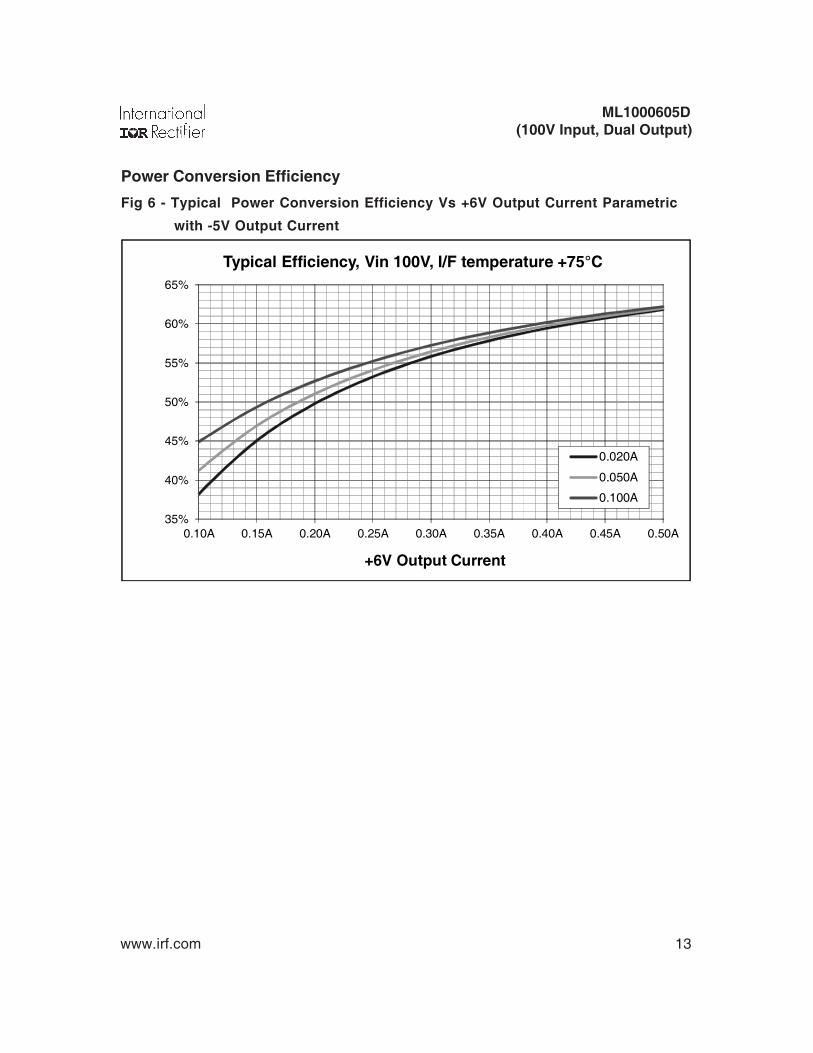
Fig 6 - Typical Power Conversion Efficiency Vs +6V Output Current Parametric
Power Conversion Efficiency
35%
40%
45%
50%
55%
60%
65%
0.10A 0.15A 0.20A 0.25A 0.30A 0.35A 0.40A 0.45A 0.50A
+6V Output Current
Typical Efficiency, Vin 100V, I/F temperature +75°C
0.020A
0.050A
0.100A
with -5V Output Current

14 www.irf.com
ML1000605D(100V Input, Dual Output)
Recommended Mounting Stud DesignIt is foreseen with a mounting stud design with circular mounting studs made out of aluminum with adiameter of 4.0mm and a treaded hole support mounting with M2 screws.
5pcs M2 screws are used for mounting the board. Mounting torque shall be 30Ncm ± 5.0Ncm.
www.irf.com 15
ML1000605D (100V Input, Dual Output)
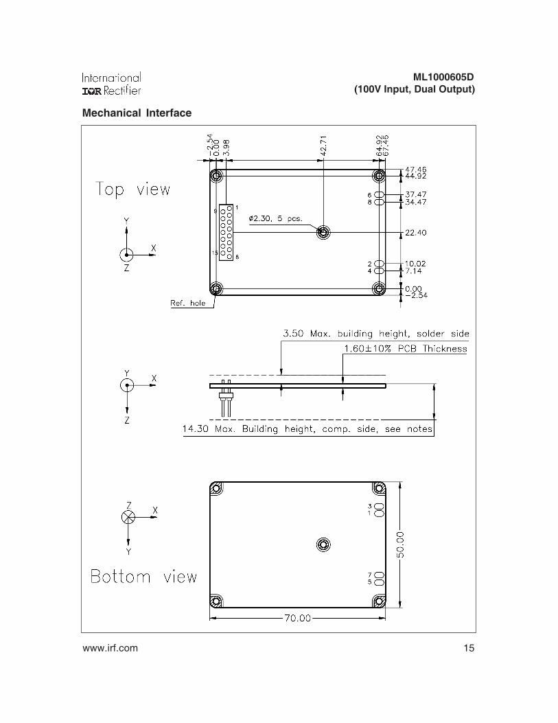
Mechanical Interface
16 www.irf.com
ML1000605D(100V Input, Dual Output)
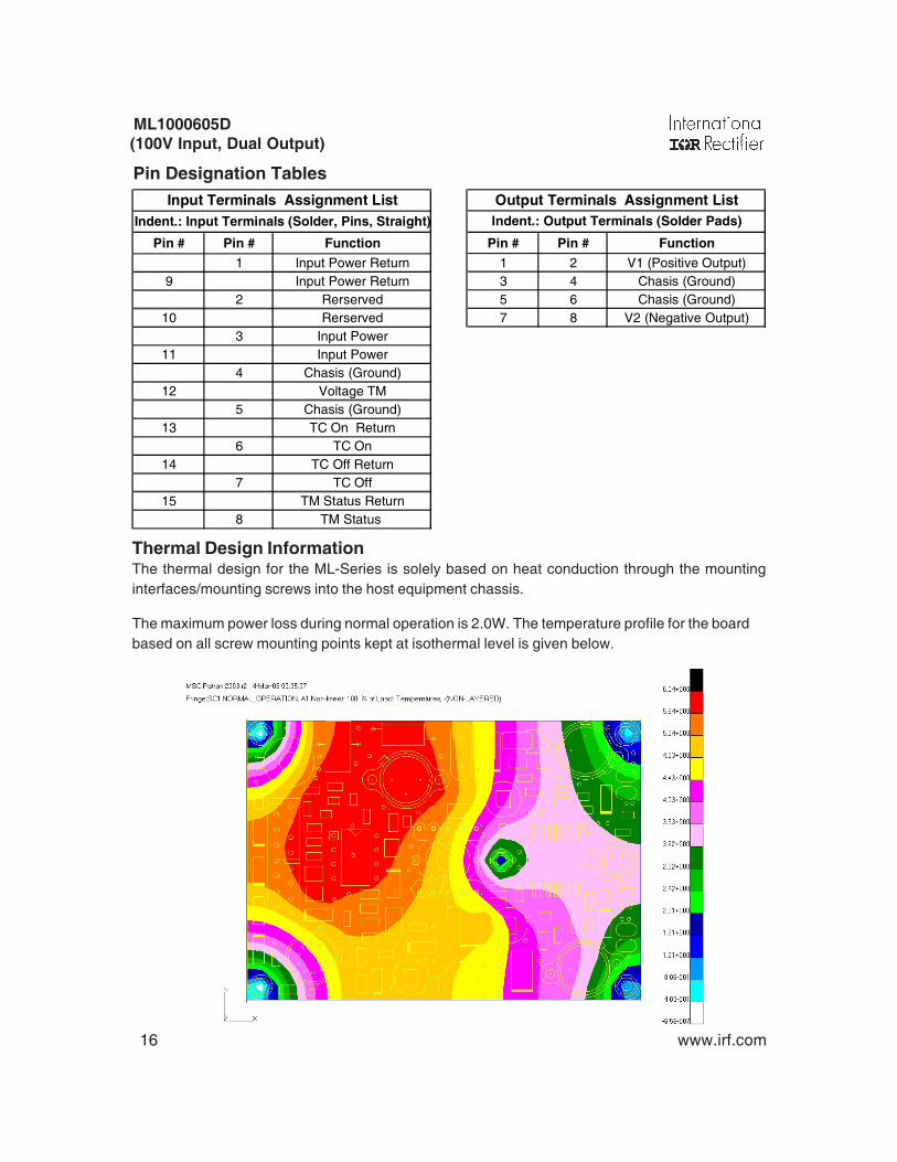
Pin Designation Tables
Thermal Design InformationThe thermal design for the ML-Series is solely based on heat conduction through the mountinginterfaces/mounting screws into the host equipment chassis.
The maximum power loss during normal operation is 2.0W. The temperature profile for the boardbased on all screw mounting points kept at isothermal level is given below.
Pin # Pin # Function
1 Input Power Return9 Input Power Return
2 Rerserved10 Rerserved
3 Input Power11 Input Power
4 Chasis (Ground)12 Voltage TM
5 Chasis (Ground)13 TC On Return
6 TC On14 TC Off Return
7 TC Off15 TM Status Return
8 TM Status
Indent.: Input Terminals (Solder, Pins, Straight)
Input Terminals Assignment List
Pin # Pin # Function
1 2 V1 (Positive Output)3 4 Chasis (Ground)5 6 Chasis (Ground)7 8 V2 (Negative Output)
Output Terminals Assignment ListIndent.: Output Terminals (Solder Pads)
www.irf.com 17
ML1000605D (100V Input, Dual Output)
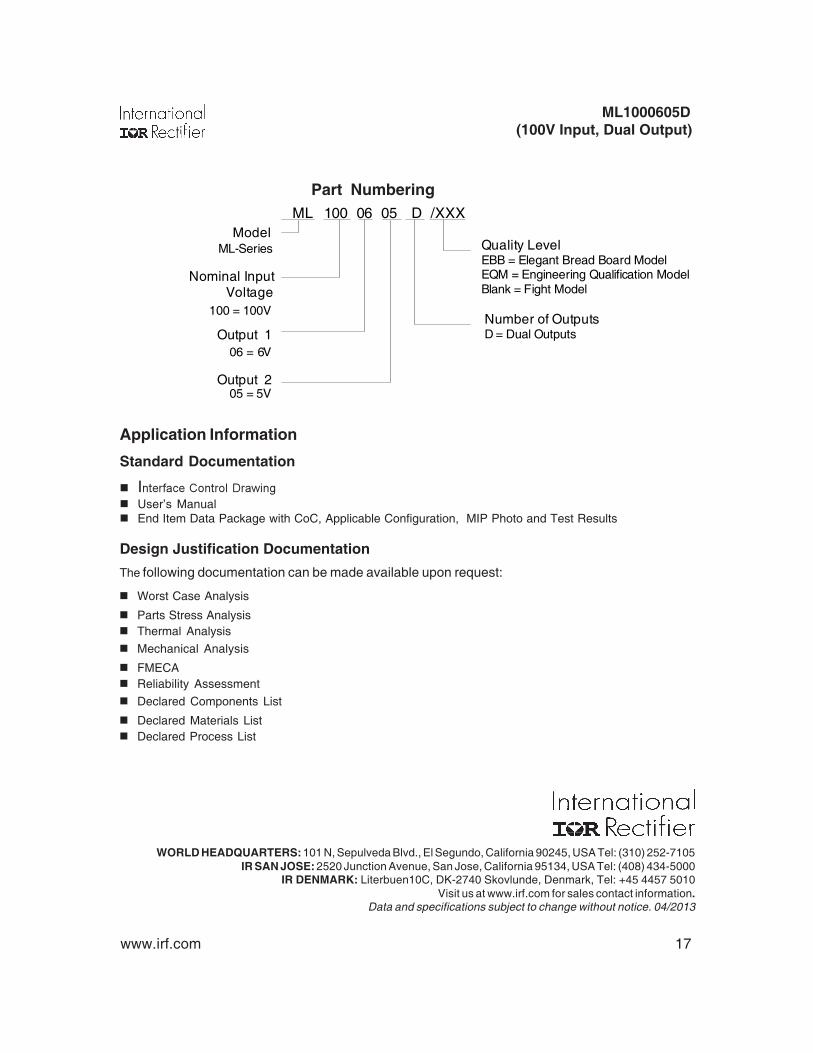
Part Numbering
WORLD HEADQUARTERS: 101 N, Sepulveda Blvd., El Segundo, California 90245, USA Tel: (310) 252-7105IR SAN JOSE: 2520 Junction Avenue, San Jose, California 95134, USA Tel: (408) 434-5000
IR DENMARK: Literbuen10C, DK-2740 Skovlunde, Denmark, Tel: +45 4457 5010Visit us at www.irf.com for sales contact information.
Data and specifications subject to change without notice. 04/2013
Application Information
Standard Documentation
User’s Manual End Item Data Package with CoC, Applicable Configuration, MIP Photo and Test Results
Design Justification Documentation
The following documentation can be made available upon request:
Worst Case Analysis
Parts Stress Analysis Thermal Analysis
Mechanical Analysis
FMECA Reliability Assessment
Declared Components List
Declared Materials List Declared Process List
Output 1
Model
Nominal Input Voltage
100 = 100V
06 = 6V
Number of OutputsD = Dual Outputs
Quality LevelEBB = Elegant Bread Board ModelEQM = Engineering Qualification ModelBlank = Fight Model
ML-Series
Output 205 = 5V
ML 100 06 05 D /XXX