data sheet, rev. 1 - reactivedata.com · rev. 1.2 mdoc h3 efd featuring embedded trueffs data sheet...
TRANSCRIPT

© 2007 SanDisk® Corporation 1 92-DS-1205-10
mDOC H3 Embedded Flash Drive (EFD) featuring Embedded TrueFFS®
Flash Management Software Data Sheet, November 2007
HIGHLIGHTS mDOC H3 is an Embedded Flash Drive (EFD) designed for mobile handsets and consumer electronics devices. mDOC H3 is the new generation of SanDisk’s successful mDOC product family, enabling tens of millions of handsets and other mobile devices since the year 2000.
mDOC H3 is a hybrid device combining an embedded thin flash controller and standard flash memory.
In addition to the high reliability and high system performance offered by the current mDOC family of products, mDOC H3 offers plug-and-play integration, support for multiple NAND technologies and more features such as advanced power management schemes.
mDOC H3 uses advanced Multi-Level Cell (MLC) and binary (SLC) NAND flash technologies, enhanced by SanDisk’s proprietary TrueFFS embedded flash management software running as firmware on the flash controller.
The breakthrough in performance, size, cost and design makes mDOC H3 the ideal solution for mobile handsets and consumer electronics manufacturers who require easy integration, fast time to market, high-capacity, small form factor, high-performance and most importantly, highly reliable storage.
mDOC H3 enables multimedia driven applications such as music, photo, video, TV, GPS, games, email, office and other applications.
EMBEDDED TRUEFFS SanDisk’s proprietary TrueFFS flash management software is now embedded within the mDOC H3 device and runs as firmware from the flash controller.
Legacy mDOCArchitecture
HostFlash
Controller Flash + + +
mDOCH3 Architecture
HostFlash
Controller Flash + + +
Legacy mDOCArchitecture
HostFlash
Controller Flash + + +HostFlash
Controller Flash + + +
mDOCH3 Architecture
HostFlash
Controller Flash + + +HostFlash
Controller Flash + + +
Figure 1: TrueFFS - Legacy mDOC vs. mDOC H3 Architecture
Embedded TrueFFS enables mDOC H3 to fully emulate a hard disk to the host processor,

Rev. 1.2 mDOC H3 EFD Featuring Embedded TrueFFS Data Sheet
2 92-DS-1205-10
enabling read/write operations that are identical to a standard, sector-based hard drive. In addition, Embedded TrueFFS employs patented methods, such as virtual mapping, dynamic and static wear-leveling, and automatic block management to ensure high data reliability and maximize flash life expectancy.
Furthermore, it provides performance enhancements such as multi-plane operations, DMA support, Burst operation and Dual Data RAM buffering.
mDOC H3 extended features are enabled by a small driver that runs on the host side, called DOC Driver. DOC Driver provides the host OS with a standard Block Device interface. The combination of Embedded TrueFFS and DOC Driver enables a practically Plug & Play integration in the system.
PLUG-AND-PLAY INTEGRATION mDOC H3 optimized architecture with Embedded TrueFFS eliminates the need for complicated software integration and testing processes and enables a practically plug-and-play integration in the system.
The replacement of one mDOC H3 device with another, of a newer generation, requires virtually no changes to the host. This makes mDOC H3 the perfect solution for platforms and reference designs, as it allows for the utilization of more advanced NAND Flash technology with minimal integration or qualification efforts.
Embedded TrueFFS running from mDOC H3 means there is no need to modify and re-qualify the flash management software on the host system, or update mass production tools.
MULTIPLE FLASH SUPPORT
mDOC H3 with Embedded TrueFFS enables access to advanced binary SLC NAND and MLC NAND flash technology, making mDOC H3 the only multi-sourced and multi-technology EFD.
Embedded TrueFFS overcomes SLC and MLC NAND-related error patterns by using a robust error detection and correction (EDC/ECC) mechanism.
mDOC H3 optimized architecture with Embedded TrueFFS offers high reliability and high system performance for whatever flash technology or density utilized.
MDOC H3 PROVIDES: Flash disk for both code and data storage Code and data storage protection Low voltage:
1.8V Core and I/O 3.3V Core and 3.3V/1.8V I/O (auto-detect)
Typical Current Consumption Turbo mode: 30mA Power Save mode: 20mA Standby mode: 5mA Deep Power-Down mode: 60uA-
110uA 1Gb (128MB) – 64Gb (8GB) data storage
capacity, with device cascading options for up to 128Gb (16GB).
Enhanced Programmable Boot Block (32KB) enabling eXecute In Place (XIP) functionality using 16-bit access.
Small form factors: mDOC H3 1Gb/2Gb - 115-ball
Fine-Pitch Ball Grid Array (FBGA) 9x12mm.
mDOC H3 4Gb/8Gb - 115-ball Fine-Pitch Ball Grid Array (FBGA) 10x14mm.

Rev. 1.2 mDOC H3 EFD Featuring Embedded TrueFFS Data Sheet
3 92-DS-1205-10
mDOC H3 8Gb/16Gb/32Gb/64Gb - 115-ball Fine-Pitch Ball Grid Array (FBGA) 12x18mm
Ball to ball compatible with mDOC G3/G4/H1 families.
Enhanced performance by implementation of:
Multi-plane operations DMA support Burst operation Dual Data RAM buffering Read/Write Cache Fast partition configuration
Powerful data integrity with a robust Error Detection Code/Error Correction Code (EDC/ECC) specifically tailored for the most advanced flash technology.
Strong flash endurance with TrueFFS
advanced flash management software. Reduced complexity for the host system by
moving flash management functionality to the device.
Plug & Play integration with the host system, due to embedding TrueFFS within the device itself.
Support for major mobile operating systems (OSs), including Symbian OS, Windows Mobile, Windows CE, Linux and more.
Compatibility with major mobile CPUs Performance:
Sustained write: 4-8 MB/sec. Sustained read: 15-25 MB/sec
PROTECTION & SECURITY-ENABLING
16-byte Unique Identification (UID) number.
14 configurable protected partitions for data and code:
Write protected Read and Write protected One Time Programmable (OTP)
Protection key and LOCK# signal Sticky Lock (SLOCK) to lock boot
partition Protected Bad Block Table.
RELIABILITY AND DATA INTEGRITY Hardware on-the-fly Error Detection
Code/Error Correction Code (EDC/ECC), based on a BCH algorithm, tailored for the most advanced flash technology.
Data integrity after power failure. Transparent bad-block management. Dynamic and static wear-leveling.
BOOT CAPABILITY 32KB Programmable Boot Block with XIP
capability to replace boot ROM or NOR. 254KB Paged RAM IPL Boot Agent for automatic download of
boot code to the Programmable Boot Block.
Asynchronous Boot mode to enable ARM-based CPUs, e.g. TI OMAP, Intel PXAxxx, to boot without the need for external glue logic.
Exceptional boot performance with Burst operation and DMA support enhanced by external clock.
HARDWARE COMPATIBILITY Configurable interface: simple SRAM-like
or multiplexed address/data interface. CPU compatibility, including:
ARM-based CPUs Texas Instruments OMAP, DBB Marvell PXAxxx family Infineon xGold family Analog Devices (ADI) digital
Baseband devices Freescale i.MXxx Application
processors and i.xx digital Baseband devices

Rev. 1.2 mDOC H3 EFD Featuring Embedded TrueFFS Data Sheet
4 92-DS-1205-10
Zoran ER4525 Renesas SH mobile EMP platforms Qualcomm MSMxxxx Hitachi SuperH™ SH-x
Supports 16 and 32-bit architectures
EMBEDDED TRUEFFS SOFTWARE TrueFFS (True Flash File System) is SanDisk’s field proven patented flash management software. TrueFFS is embedded within the mDOC H3 device, providing full Block Device functionality to the Operating System (OS) file system via either TrueFFS 7.1 (for supporting both earlier mDOC products and mDOC H3) or the DOC Driver. TrueFFS allows for mDOC H3 to appear to the OS as a regular hard drive, while at the same time transparently providing robust flash media management.
DOC Driver provides full block device emulation for transparent file system management
Disk-like interface Dynamic virtual mapping Automatic bad block management Dynamic and static wear-leveling Programming, duplicating and testing tools
available in source code
CAPACITY AND PACKAGING 1Gb (128MB) – 64Gb (8GB) capacity,
with device cascading option for up to two devices (128Gb).
FBGA package: 115 balls, 9x12x1.2 mm (width x length x height)
FBGA package: 115 balls, 10x14x1.2 mm (width x length x height)
FBGA package: 115 balls, 12x18x1.4 mm and 12x18x1.2 mm (width x length x height)
Ball-out compatible with mDOC G3, G4 and H1 products: Refer to Migration Guide mDOC G3-P3 G3P3-LP G4 H1 to mDOC H3 for further details.
OPERATING ENVIRONMENT Wide OS support, including:
Symbian OS Windows Mobile Windows CE Linux Nucleus OSE PalmOS
DOC Driver Software Development Kit (SDK) for quick and easy support of proprietary OSs or OS-less environments.

Rev. 1.2 mDOC H3 EFD Featuring Embedded TrueFFS Data Sheet
5 92-DS-1205-10
REVISION HISTORY
Doc. No Revision Date Description Reference 0.1 January 2006 Preliminary version
RSRVD balls left floating changed from a recommendation to a requirement
Section 2
Demux (Standard) I/F Ball H9 changed from RSRVD to VSS
Section 2.2
Ballout change – Some NC balls removed, resulting in 115 balls for all products
Section 2.2
Ball H2 changed from DPD to A0 Sections 2.2 and 2.3
Details on internal pull up and pull down resistors added
Sections 2.2.2 and 2.3.2
DPD signal removed (replaced with A0, which should be connected to CPU A0 or to VSS)
Sections 2, 2.2.2 and 2.3.2
Balls G1,H1,J1,K1 marked as reserved
Ball G4 changed from RSRVD to VCCQ
Sections 2.2.2 and 2.3.2
Ball D9 changed from NC to RSRVD
Section 2.3.2
Modes of operation diagram updated
Section 5
“Normal mode” name changed to “Turbo mode”
Section 5
8KB address space settings added Section 6.5
Added register addresses for 8KB address space
Section 7
Burst mode can only be used in conjunction with mDOC H3 DMA functionality
Section 9.8.2
Operating Conditions updated Section 10.3
Asynchronous boot mode timing diagram added
Section 10.3.1
Multiplexed timing updated Section 10.3.4
Section 10.3.5
Power up timing updated Section 10.3.11
92-DS-1205-10
0.2 June 2006
Mechanical drawing updated (removed balls from 12x18mm drawing)
Section 10.4.3

Rev. 1.2 mDOC H3 EFD Featuring Embedded TrueFFS Data Sheet
6 92-DS-1205-10
Doc. No Revision Date Description Reference Ordering information modified Section 11
Refer to Standard Interface as Demux
Entire Document
Current/Power consumption numbers modified
Highlights and Section 10.2.3
Number of partitions available changed from 10 to 14
Highlights and Section 2.1
Note that CLK should be half-frequency at Power-Save mode
Section 10.3
Added clarifications about capacitor requirements for different voltage configurations
Section 9.5
Marking section added Section 0
BUSY#, DMARQ# and IRQ#: changed from CMOS 3-STATE to CMOS output and added clarification about pull ups
Table 1 and Table 2
Key size modified Section 4
Modes of operation section enhanced
Section 5
mDOC H3 registers section updated
Section 7
GPIO_TIMER and WARM_RST# description updated
Entire Document
Synchronous Burst Operation description modified
Section 9.8.2
Storage temperature modified and section enhanced
Section 10.2.1
Demux asynchronous read access time modified; Tdh max added; Tah, Tw(oeh) and Tw(oel) added
Section 10.3.2
Demux asynchronous write timing – Tw(wel) and Tw(weh) added
Section 10.3.2
Demux burst read minimal clock cycle time modified
Section 10.3.6
Mechanical dimensions tolerance corrected
Section 10.4
Power up timing section updated Section 10.3.12
Max input fall and rise time info added
Section 10.3.1
1.0 February 2007
Figure modified Figure 9

Rev. 1.2 mDOC H3 EFD Featuring Embedded TrueFFS Data Sheet
7 92-DS-1205-10
Doc. No Revision Date Description Reference Add 10x14 package size Sections 2.2, 2.3
Paragraph revisited Section 3.5
Change requirement for capacitor on VCC
Section 9.5
Modified comment 14
Add comment 17 Section 9.5
Added drawings to depict power connectivity
Section 9.5
Added temperature range for new products
Section 10.1.1
DC characteristics: added disclaimer for Icc / Iccs parameters for new products
Section 10.2.3
Updated parameter Tcesu Sections 10.3.6, 10.3.8
Add 10x14 package mechanical description
Section 10.4.2
Added note on ball size change of new products
Sections 10.4.1, 10.4.3
Ordering info section updated Section 11
Added new SanDisk top marking Section 12
128KB window updated Section 6.4
1.1 April/May 2007
Updated DMA transfer timing diagram
Section 10.3.9
Remove internal pull up of #AVD signal
Section 2.3.2
Updated Icc max values for new products
Table 9
Multiplexed Synchronous write timing updated
Section 10.3.4
Mechanical dimension updated: ball size reduced for 9x12 package
Section 10.4.1
Marking section revised Section 12
92-DS-1205-10 1.2 November 2007
Burst mode section revised Section 9.8.2
mDOC 8GB product added Entire document

Rev. 1.2 mDOC H3 EFD Featuring Embedded TrueFFS Data Sheet
8 92-DS-1205-10
TABLE OF CONTENTS 1. Introduction..............................................................................................................................12 2. Product Overview ....................................................................................................................13
2.1 Product Description ..........................................................................................................13
2.2 Demux (Standard) Interface .............................................................................................14 2.2.1 9x12/10x14/12x18 FBGA Ball Diagrams ............................................................................14 2.2.2 9x12/10x14/12x18 FBGA Signal Description......................................................................16 2.2.3 System Interface .................................................................................................................19
2.3 Multiplexed Interface.........................................................................................................19 2.3.1 9x12/10x14/12x18 FBGA Ball Diagram ..............................................................................19 2.3.2 9x12/10x14/12x18 FBGA Signal Description......................................................................21 2.3.3 System Interface .................................................................................................................23
3. Theory of Operation ................................................................................................................25 3.1 Overview...........................................................................................................................25
3.2 Host Interface ...................................................................................................................26 3.2.1 Demux (NOR-Like) Interface...............................................................................................26 3.2.2 Multiplexed Interface ...........................................................................................................26 3.2.3 Serial Interface ....................................................................................................................27
3.3 Host Agent ........................................................................................................................27 3.3.1 Host Protocol.......................................................................................................................27 3.3.2 Boot Block (XIP)..................................................................................................................27
3.4 Boot Agent ........................................................................................................................27
3.5 Error Detection Code/Error Correction Code (EDC/ECC) ................................................28
3.6 Block Device Management ...............................................................................................28
4. Data Protection and Security-Enabling features ..................................................................29 4.1.1 Read/Write-Protected partitions..........................................................................................29 4.1.2 LOCK# signal ......................................................................................................................29 4.1.3 Sticky Lock (SLOCK) ..........................................................................................................29 4.1.4 Unique Identification (UID) Number ....................................................................................30 4.1.5 One-Time Programmable (OTP) Partitions.........................................................................30
5. mDOC H3 Modes of Operation ...............................................................................................31 5.1 Reset State.......................................................................................................................32
5.2 Turbo Mode ......................................................................................................................32
5.3 Power Save Mode ............................................................................................................32
5.4 Standby Mode...................................................................................................................32
5.5 Deep Power-Down Mode..................................................................................................33

Rev. 1.2 mDOC H3 EFD Featuring Embedded TrueFFS Data Sheet
9 92-DS-1205-10
6. Embedded TrueFFS Technology............................................................................................34 6.1 General Description..........................................................................................................34
6.2 Operating System Support ...............................................................................................34
6.3 DOC Driver Software Development Kit (SDK)..................................................................35 6.3.1 File Management ................................................................................................................35 6.3.2 Bad-Block Management......................................................................................................35 6.3.3 Wear-Leveling .....................................................................................................................35 6.3.4 Power Failure Management ................................................................................................36 6.3.5 Error Detection/Correction ..................................................................................................36 6.3.6 Special Features through I/O Control (IOCTL) Mechanism................................................36 6.3.7 Compatibility........................................................................................................................37
6.4 128KB Memory Window ...................................................................................................37
6.5 8KB Memory Window .......................................................................................................39
7. mDOC H3 Registers ................................................................................................................40 7.1 Definition of Terms............................................................................................................40
7.2 Reset Values ....................................................................................................................40
7.3 Registers Description........................................................................................................41 7.3.1 Paged RAM Command Register.........................................................................................41 7.3.2 Paged RAM Select Register ...............................................................................................41 7.3.3 Paged RAM Unique ID Download Register ........................................................................42 7.3.4 Chip Identification (ID) Register [0:1] ..................................................................................42 7.3.5 Burst Mode Control Registers (Read & Write) ....................................................................42 7.3.6 Burst Write Mode Exit Register ...........................................................................................43 7.3.7 DPD Wakeup Trigger Register............................................................................................43 7.3.8 DPD Activation Register......................................................................................................44 7.3.9 DMA Control Register .........................................................................................................44 7.3.10 DMA Negation Register ......................................................................................................45 7.3.11 Software Lock Register .......................................................................................................45 7.3.12 Endian Control Register ......................................................................................................46
8. Booting from mDOC H3 ..........................................................................................................47 8.1 Introduction.......................................................................................................................47
8.1.1 Asynchronous Boot Mode...................................................................................................48 8.1.2 Paged RAM Boot ................................................................................................................48
9. Design Considerations ...........................................................................................................49 9.1 General Guidelines...........................................................................................................49
9.2 Configuration ....................................................................................................................49
9.3 Demux (Standard) Interface .............................................................................................49
9.4 Multiplexed Interface.........................................................................................................50

Rev. 1.2 mDOC H3 EFD Featuring Embedded TrueFFS Data Sheet
10 92-DS-1205-10
9.5 mDOC H3 Power Supply Connectivity .............................................................................51
9.6 Connecting Control Signals ..............................................................................................55 9.6.1 Demux Interface..................................................................................................................55 9.6.2 Multiplexed Interface ...........................................................................................................55
9.7 Implementing the Interrupt Mechanism ............................................................................56 9.7.1 Hardware Configuration ......................................................................................................56 9.7.2 Software Configuration........................................................................................................56
9.8 DMA and Burst Operation.................................................................................................56 9.8.1 DMA Operation ...................................................................................................................56 9.8.2 Synchronous Burst Operation.............................................................................................57
9.9 Device Cascading.............................................................................................................60
9.10 Platform-Specific Issues ...................................................................................................61 9.10.1 Wait State............................................................................................................................61 9.10.2 Big and Little Endian Systems ............................................................................................61 9.10.3 Busy Signal .........................................................................................................................61 9.10.4 Working with 16/32-Bit Systems .........................................................................................61
9.11 Design Environment .........................................................................................................63
10. Product Specifications............................................................................................................64 10.1 Environmental Specifications............................................................................................64
10.1.1 Operating Temperature.......................................................................................................64 10.1.2 Thermal Characteristics ......................................................................................................64 10.1.3 Humidity ..............................................................................................................................64
10.2 Electrical Specifications....................................................................................................64 10.2.1 Absolute Maximum Ratings ................................................................................................64 10.2.2 Capacitance ........................................................................................................................65 10.2.3 DC Characteristics ..............................................................................................................65
10.3 Timing Specifications........................................................................................................68 10.3.1 Operating Conditions ..........................................................................................................68 10.3.2 Demux Asynchronous Read Timing ...................................................................................69 10.3.3 Demux Asynchronous Write Timing....................................................................................70 10.3.4 Multiplexed Asynchronous Read Timing.............................................................................70 10.3.5 Multiplexed Asynchronous Write Timing.............................................................................71 10.3.6 Demux Burst Read Timing ..................................................................................................72 10.3.7 Demux Burst Write Timing ..................................................................................................73 10.3.8 Multiplexed Burst Read Timing ...........................................................................................74 10.3.9 DMA Request Timing Diagram ...........................................................................................75 10.3.10 SPI Timing...........................................................................................................................76 10.3.11 Power Supply Sequence.....................................................................................................77 10.3.12 Power-Up Timing ................................................................................................................77

Rev. 1.2 mDOC H3 EFD Featuring Embedded TrueFFS Data Sheet
11 92-DS-1205-10
10.4 Mechanical Dimensions....................................................................................................79 10.4.1 mDOC H3 1Gb (128MB)/2Gb (256MB) ..............................................................................79 10.4.2 mDOC H3 4Gb (512MB)/8Gb (1GB) ..................................................................................80 10.4.3 mDOC H3 8Gb (1GB)/ 16Gb (2GB)/ 32Gb (4GB) / 64Gb (8GB)........................................81
11. Ordering Information...............................................................................................................82 12. Markings...................................................................................................................................83
12.1 mDOC H3 1Gb (128MB)/2Gb (256MB) ............................................................................83
12.2 mDOC H3 8Gb (1GB)/16Gb (2GB) ..................................................................................84
12.3 mDOC H3 2Gb (256MB)/ 4Gb (512MB)/ 8Gb (1GB)/ 16Gb (2GB)/ 32Gb (4GB) / 64Gb (8GB)...............................................................................................................................85
Disclaimer of Liability ...................................................................................................................86

Rev. 1.2 Introduction
mDOC H3 EFD Featuring Embedded TrueFFS Data Sheet
© 2007 SanDisk® Corporation 12 92-DS-1205-10
1. INTRODUCTION This data sheet includes the following sections:
Section 1: Introduction and overview of data sheet contents
Section 2: Product overview, including a brief product description, ball diagrams and signal descriptions
Section 3: Theory of operation for the major building blocks
Section 4: Data protection and security enabling features overview
Section 5: Detailed description of modes of operation
Section 6: Embedded TrueFFS Technology overview, including power failure management and 8KB/128KByte memory window
Section 7: mDOC H3 register descriptions
Section 8: Overview of how to boot from mDOC H3
Section 9: Hardware and software design considerations
Section 10: Environmental, electrical, timing and product specifications
Section 11: Information on ordering mDOC H3
Section 12: Marking information
For additional information on SanDisk’s flash disk products, please contact one of the offices listed on the back page.

Rev. 1.2 Product Overview
mDOC H3 EFD Featuring Embedded TrueFFS Data Sheet
13 92-DS-1205-10
2. PRODUCT OVERVIEW
2.1 Product Description mDOC H3 is the latest addition to SanDisk’s mDOC product family. mDOC H3, packaged in a small FBGA package and offering densities ranging from 1Gb (128MB) to 16Gb (2GB), is a hybrid device with an embedded flash controller and high capacity flash memory. It uses advanced Flash technologies, enhanced by SanDisk’s proprietary TrueFFS embedded flash management software.
All mDOC H3 devices are ball to ball compatible. The replacement of one mDOC H3 device with another of a newer generation requires virtually no changes to the host. This makes mDOC H3 the perfect solution for platforms and reference designs, as it allows for the utilization of more advanced NAND Flash technology and new mDOC functionality with minimal integration efforts.
mDOC H3 has a 32KB Programmable Boot Block. This block provides eXecute In Place (XIP) functionality, enabling mDOC H3 to replace the boot device and to function as the only non-volatile memory device on-board. Eliminating the need for an additional boot device reduces hardware expenditures, board real estate, programming time, and logistics. The Paged RAM IPL feature separates the Boot Block into sections: The first section provides constant data, while the other sections (up to 254KB) can be loaded with data that is automatically downloaded from the flash. One application of this feature is to support processors’ secure boot requirements.
Sandisk’s proprietary TrueFFS flash management software overcomes NAND-related error patterns by using a robust error detection and correction (EDC/ECC) mechanism. Furthermore, it provides performance enhancements such as multi-plane operations, DMA support, Burst operation and Dual Data RAM buffering.
The new generation of patented flash management software, Embedded TrueFFS, is run on the embedded thin controller of the mDOC H3 device, instead of on the host. This results in improvements in performance, ease of integration and overall utilization of latest NAND technologies. Embedded TrueFFS guarantees high reliability and isolates all the complexity of flash management from the host SW.
Embedded TrueFFS enables mDOC H3 to fully emulate a hard disk to the host processor, enabling read/write operations that are identical to a standard, sector-based hard drive. In addition, Embedded TrueFFS employs patented methods, such as virtual mapping, dynamic and static wear-leveling, and automatic bad block management to ensure high data reliability and maximize flash life expectancy. mDOC H3 extended features are enabled by a small driver that runs on the host side, called DOC Driver. DOC Driver provides the host O/S with a standard Block Device interface, together with APIs for mDOC H3’s extended features. The combination of Embedded TrueFFS and DOC Driver practically enables Plug and Play integration.
mDOC H3 offers extended content protection and security-enabling features. Up to 14 write protected, read-and-write protected, or One Time Programmable (OTP) partitions can be configured independently for maximum design flexibility. A 16-byte Unique ID (UID) identifies each device, eliminating the need for a separate ID device on the motherboard. The combination

Rev. 1.2 Product Overview
mDOC H3 EFD Featuring Embedded TrueFFS Data Sheet
14 92-DS-1205-10
of these features enables mDOC H3 to implement better security schemes to protect the code and data it stores.
mDOC H3 can be configured to work with either demux (standard) interface or multiplexed (MUX) interface. Using a multiplexed interface where data and address lines are multiplexed on the same lines, reduces the number of signals required to connect mDOC H3 to the CPU.
The combination of unique H3 design, latest NAND technology and Embedded TrueFFS results in a low-cost, minimal-sized flash disk that achieves unsurpassed reliability levels, enhanced performance and ease of integration.
This breakthrough in performance, size, cost and design makes mDOC H3 the ideal solution for mobile handsets and consumer electronics manufacturers who require easy integration, fast time to market, high-capacity, small size, high-performance and, above all, high-reliability storage to enable multimedia driven applications such as music, photo, video, TV, GPS, games, email, office and other applications.
mDOC H3 offers advanced power consumption management throughout the selection of different operating modes. The operating modes of the mDOC H3 device are designed to be easily controlled by the chipset and DOC Driver to ensure optimal battery life in mobile devices.
mDOC H3 can be placed in any of the following four operating modes: • Turbo mode - While in Turbo mode, device internal clocks are optimized for maximal
performance. • Power Save mode – While in Power Save mode, device internal clocks are optimized to
balance between device performance and power consumption. • Standby mode – While in Standby mode, the clock of most internal cores is either
disconnected or reduced to a minimum. There is no wake-up time penalty. • Deep Power Down (DPD) mode - While in Deep Power-Down mode, device quiescent
power dissipation is reduced by disabling internal high current consumers (e.g. flash, voltage regulators, input buffers, oscillator etc.)
The power management flexibility of mDOC H3 allows for the system designers to substantially reduce the power consumption of the mDOC device, based on the requirements of the mobile device, to effectively and considerably prolong battery life.
2.2 Demux (Standard) Interface
2.2.1 9x12/10x14/12x18 FBGA Ball Diagrams
Figure 2 shows the mDOC H3 115 ball demux interface ball diagram.
To ensure proper device functionality, balls marked RSRVD are reserved for future use and should be connected as described in Table 1, Section 2.2.2.
Note: mDOC H3 is designed as a ball to ball compatible with mDOC G3, G4 and H1 products, assuming that the latter were integrated according to the guidelines in the migration guide. Refer to Migration Guide mDOC G3-P3 G3P3-LP G4 H1 to mDOC H3, for further information.

Rev. 1.2 Product Overview
mDOC H3 EFD Featuring Embedded TrueFFS Data Sheet
15 92-DS-1205-10
9x12/10x14/12x18 FBGA Package
Figure 2: Demux Interface Ball Diagram for 9x12, 10x14 and 12x18 FBGA – Top View
D5D2D 8 D11 D14
A9A13 C- LOCK#A 2 BUSY# RSRVD A 5
WARM_ RST # D4 D15D3CE # D9 D13
VCCQD 0 SCLKRSRVD D10 VCC D12
RSRVDRSRVD RSRVDRSRVD RSRVD RSRVD RSRVDRSRVD RSRVD RSRVD
NCNC RSRVD NC
A8VSS VCC2 WE# A11A 7
A 6 C+ A12VCC1RSTIN#A14 A 15A3
SCS#A 1 IRQ # ID0A 4 VCCQ A10NCNCRSRVD
VSS D1RSRVD D6NCNC SO
NC NC NCRSRVD
NC NC NCNC
NC NC NCNC
RSRVD RSRVD RSRVD RSRVDRSRVD RSRVD RSRVD RSRVD RSRVD
RSRVD RSRVD
RSRVD
A 16
SI
VSS RSRVD
RSRVD
RSRVD RSRVD RSRVD RSRVD
RSRVD
GPIO _ TIMER
CLK
DMARQ#A0
RSRVD
VSS
OE #
D7
RSRVD
9 101 2 3 4 5 6 7 8
A
B
C
D
E
F
G
H
J
K
L
M
N
P

Rev. 1.2 Product Overview
mDOC H3 EFD Featuring Embedded TrueFFS Data Sheet
16 92-DS-1205-10
2.2.2 9x12/10x14/12x18 FBGA Signal Description
mDOC H3 (115 ball) package ball designations are listed in the signal descriptions, presented in logic groups, in Table 1.
Table 1: Demux Interface Signal Description
Signal Ball No. Signal Type1 Description Signal Direction
System Interface
A[16:15] A[14:13] A[12:11] A[10:8] A[7:4] A[3:0]
F10, E10 E4, F4 E8, D8
G7, F7, D7 D3, E3, F3, G3 E2, F2, G2, H2
A[12:0] ST A[16:13]IN/PD Address bus.
Input
D[7:6] D[5:3] D[2:0]
K8, H7 L7, J6, J5 L4, H4, K3
ST Data bus, low byte.
Input/output
D[15:14] D[13:12] D[11:8]
J8, L8 J7, K7
L5, K4, J4, L3
ST
Data bus, high byte.
Input/output
CE# J2 ST Chip Enable, active low. Input OE# J3 ST Output Enable, active low. Input WE# D6 ST Write Enable, active low Input
Configuration
GPIO_TIMER E1 ST/PU RSRVD. This signal may be left floating or pulled up.
Input/output
ID0 G8 PD
Identification. Configuration control to support up to two chips cascaded in the same memory window. Chip 1: ID0 = VSS Chip 2: ID0 = VCCQ
Input
LOCK# F8 ST Lock, active low. When active, provides full hardware data protection of selected partitions.
Input
Control
WARM_RST# J9 ST/PU RSRVD. This signal may be left floating or pulled up.
Input
BUSY# F5 CMOS output Busy. Active low. Indicates that mDOC is initializing and should not be accessed5
Output
RSTIN# E5 ST/PU Reset, active low. input

Rev. 1.2 Product Overview
mDOC H3 EFD Featuring Embedded TrueFFS Data Sheet
17 92-DS-1205-10
Signal Ball No. Signal Type1 Description Signal Direction
CLK L6 ST External clock input used for burst mode data transfers. If not used may be left floating.
Input
DMARQ# H8 CMOS output DMA request. If not used may be left floating5.
Output
IRQ# G9 CMOS output Interrupt Request. Active low. If not used may be left floating. 5
Output
Serial Interface
SCS# G10 ST/PU/CMOS 3-STATE
Serial Interface chip select. Active low. If not used may be left floating.
Input/Output
SO H10 ST/PU/CMOS 3-STATE
Serial Interface data out (In Serial slave mode) 2. If not used may be left floating.
Output/Input
SI J10 ST/PU/CMOS 3-STATE
Serial Interface data in (In serial slave mode)
2. If not used may be left floating. Input/Output
SCLK K10 ST/PU/CMOS 3-STATE
Serial Interface clock. If not used may be left floating.
Input/Output
Power VCC2 D5 - Internal supply. Supply VCC1 E7 - Internal supply. Supply
VCCQ K6, G4 - I/O power supply.
Supply
VCC K5 - Device supply. Supply
VSS D4, H3, H9, K9
- Ground. All VSS balls must be connected. Supply
C+ E6 - C1 capacitor positive terminal3. Supply C- F6 - C1 capacitor negative terminal3. Supply

Rev. 1.2 Product Overview
mDOC H3 EFD Featuring Embedded TrueFFS Data Sheet
18 92-DS-1205-10
Signal Ball No. Signal Type1 Description Signal Direction
Reserved C2, C3, C4, C5, C6, C7, C8, C9, C10, D1, D2, D9, D10, E9, F1, F9, G1, H1,
J1, K1, K2, L2, L9,
L10, M2, M3, M4,
M5, M6,M7, M8, M9,
M10
-
All reserved signals are not connected internally, and if not identified in this document then it is recommended to leave them floating to guarantee forward compatibility with future products. They should not be connected to arbitrary signals, and must not be connected to GND
P1 ST/PU Test Data In (JTAG). Used for dedicated developer product only4.
Input
M1 CMOS output Test Data Out (JTAG). Used for dedicated developer product only4.
Output
L1 ST/PU Test Mode Select (JTAG) Used for dedicated developer product only4.
Input
RSRVD
N1 ST/PU Test Clock (JTAG). Used for dedicated developer product only4.
Input
Mechanical
NC
A1, A2, A9, A10, B1, B2,
B9, B10, G5, G6, H5, H6, N2, N9, N10, P2, P9, P10
-
Not Connected.
1. The following abbreviations are used: ST - Schmitt Trigger input. IN/PD – CMOS input with internal pull down resistor (77KΩ to 312KΩ;
135KΩ typical), which is enabled only when 8KB memory window is in use, ST/PU - Schmitt Trigger input with internal pull up resistor (95KΩ to 261 KΩ; 149 KΩ typical).
2. When mDOC H3 is used as a Master device, SO is used for Serial Interface Data In, and SI is used for Serial Interface Data Out. 3. The capacitor is required only for 1.8V Core and 1.8V I/O configuration. Please see section 9.5 for further details. 4. The RSRVD JTAG balls will only be enabled on special versions of the mDOC H3 devices that will be used for debugging severe system
problems. In order to support this feature, the JTAG balls should be brought out to a separate header or test points. The JTAG RSRVD balls must not be connected to the JTAG scan chain that is used for the rest of the PCB. If not used they should be left floating.
5. BUSY#, DMARQ# and IRQ# should not be pulled up to any voltage higher than VCCQ. A pull-up resistor is required if this pin will be connected to an input. A 10K ohm resistor to Vccq is recommended, however the exact value depends on system power, timing and signal integrity requirements.

Rev. 1.2 Product Overview
mDOC H3 EFD Featuring Embedded TrueFFS Data Sheet
19 92-DS-1205-10
2.2.3 System Interface
See Figure 3 for a simplified I/O diagram of a Demux interface to mDOC H3. The power connections and capacitors in this diagram are for illustration only. For detailed recommendations regarding power connections and required capacitors, please refer to section 9.5.
For power connectivity please refer to mDOC H3 power supply connectivity in section 9.5.
Figure 3: Demux Interface Simplified I/O Diagram
2.3 Multiplexed Interface
2.3.1 9x12/10x14/12x18 FBGA Ball Diagram
Figure 4 shows the mDOC H3 115 ball multiplexed interface ball diagram. To ensure proper device functionality, balls marked RSRVD are reserved for future use and should be connected as described in Table 2, Section 2.3.2. Note: mDOC H3 designed as a ball to ball compatible with mDOC G3, G4 and H1 products, assuming that the
latter were integrated according to the guidelines in the migration guide. Refer to mDOC G3-P3 G3P3-LP G4 and H1 to mDOC H3 Migration Guide, for further information.

Rev. 1.2 Product Overview
mDOC H3 EFD Featuring Embedded TrueFFS Data Sheet
20 92-DS-1205-10
9x12/10x14/12x18 FBGA Package
Figure 4 : Multiplexed Interface Ball Diagram for 9x12/10x14/12x18 FBGA – Top View
AD5AD2AD 8 AD11 AD14
VSSVSS C- LOCK#VSS BUSY# RSRVD VSS
WARM _ RST # AD4 AD15AD3CE # AD9 AD13
VCCQAD 0 SCLKRSRVD AD10 VCC AD12
RSRVDRSRVD RSRVDRSRVD RSRVD RSRVD RSRVDRSRVD RSRVD RSRVD
NCNC RSRVD NC
VSSVSS VCC2 WE# VSSVSS
VSS C+ VSSVCC1RSTIN#VSS VSSVSS
SCS#VSS IRQ # ID0VSS VCCQ VSSNCNCRSRVD
AVD # AD1RSRVD AD6NCNC SO
NC NC NCRSRVD
NC NC NCNC
NC NC NCNC
RSRVD RSRVD RSRVD RSRVDRSRVD RSRVD RSRVD RSRVD RSRVD
RSRVD RSRVD
RSRVD
VSS
SI
VSS RSRVD
RSRVD
RSRVD RSRVD RSRVD RSRVD
RSRVD
GPIO _ TIMER
CLK
DMARQ#VSS VSS
OE #
AD7
RSRVD RSRVD
A
B
C
D
E
F
G
H
J
K
L
M
N
P
9 101 2 3 4 5 6 7 8

Rev. 1.2 Product Overview
mDOC H3 EFD Featuring Embedded TrueFFS Data Sheet
21 92-DS-1205-10
2.3.2 9x12/10x14/12x18 FBGA Signal Description
mDOC H3 FBGA related ball designations are listed in the signal descriptions, presented in logic groups, in Table 2.
Table 2: Signal Descriptions for Multiplexed Interface
Signal Ball No. Signal Type1 Description Signal Direction
System Interface
AD[15:12] AD[11:8] AD[7:4] AD[3:0]
J8, L8, J7, K7
L5, K4, J4, L3
K8, H7, L7,J6 J5,
L4, H4, K3
ST
Multiplexed bus. Address and data signals.
Input
CE# J2 ST Chip Enable, active low. Input OE# J3 ST Output Enable, active low. Input WE# D6 ST Write Enable, active low Input
Configuration
GPIO_TIMER E1 ST/PU RSRVD. This signal may be left floating or pulled up.
Input/output
AVD# H9 ST Address Valid strobe. Set multiplexed interface.
Input
ID0 G8
PD Identification. Configuration control to support up to two chips cascaded in the same memory window. Chip 1: ID0 = VSS Chip 2: ID0 = VCCQ
Input
LOCK# F8 ST Lock. Active low. When active, provides full
hardware data protection of selected partitions.
Input
Control
WARM_RST# J9 ST/PU RSRVD. This signal may be left floating or pulled up.
Input
BUSY# F5 CMOS output
Busy. Active low. Indicates that mDOC is initializing and should not be accessed. 5
Output
RSTIN# E5 ST/PU Reset, active low. Input
CLK L6 ST External clock input used for burst mode data transfers. If not used may be left floating.
Input
DMARQ# H8 CMOS output
DMA request. If not used may be left floating. 5 Output
IRQ# G9 CMOS output Interrupt Request. Active low. If not used may be left floating. 5
Output

Rev. 1.2 Product Overview
mDOC H3 EFD Featuring Embedded TrueFFS Data Sheet
22 92-DS-1205-10
Signal Ball No. Signal Type1 Description Signal Direction
Serial Interface
SCS# G10 ST/PU/CMOS 3-STATE
Serial Interface chip select. Active low. If not used may be left floating.
Input/Output
SO H10 ST/PU/CMOS 3-STATE
Serial Interface data out (In Serial slave mode)2. If not used may be left floating.
Output/Input
SI J10 ST/PU/CMOS 3-STATE
Serial Interface data in (In Serial slave mode)2. If not used may be left floating.
Input/Output
SCLK K10 ST/PU/CMOS 3-STATE
Serial Interface clock. If not used may be left floating.
Input/Output
Power VCC2 D5 - Internal supply. Supply
VCC1 E7 - Internal supply. Supply
VCCQ K6, G4 - I/O power supply. Supply
VCC K5 - Device supply. Supply
VSS D3, D4, D7, D8, E2, E3, E4 E8, E10, F2, F3, F4,
F7, F10, G2, G3, G7, H2,
H3, K9,
- Ground. All VSS balls must be connected. Supply
C+ E6 - C1 capacitor positive terminal3. Supply
C- F6 - C1 capacitor negative terminal3. Supply

Rev. 1.2 Product Overview
mDOC H3 EFD Featuring Embedded TrueFFS Data Sheet
23 92-DS-1205-10
Signal Ball No. Signal Type1 Description Signal Direction
Reserved C2, C3, C4, C5, C6, C7,
C8, C9, C10, D1, D2, D9,
D10, E9, F1, F9, G1, H1, J1, K1, K2, L2, L9, L10, M2, M3, M4, M5, M6,M7,
M8, M9, M10
-
All reserved signals are not connected internally, and if not identified in this document then it is recommended to leave them floating to guarantee forward compatibility with future products. They should not be connected to arbitrary signals.
P1 ST/PU Test Data In (JTAG).
Used for dedicated developer product only4. Input
M1 CMOS output Test Data Out (JTAG).
Used for dedicated developer product only4. Output
L1 ST/PU Test Mode Select (JTAG)
Used for dedicated developer product only4. Input
RSRVD
N1 ST/PU Test Clock (JTAG).
Used for dedicated developer product only4. Input
Mechanical
NC
A1, A2, A9, A10, B1, B2,
B9, B10, G5, G6, H5, H6, N2, N9,
N10, P2, P9, P10
-
Not Connected.
1. The following abbreviations are used: ST - Schmidt Trigger input. IN/PD – CMOS input with internal pull down resistor (77KΩ to 312KΩ; 135KΩ typical), which is enabled only when the 8KB memory window is in use, ST/PU - Schmitt Trigger input with internal pull up resistor (95KΩ to 261 KΩ; 149 KΩ typical).
2. When mDOC H3 is used as a Master device, SO is used for Serial Interface Data In, and SI used for Serial Interface Data Out. 3. The capacitor is required only for 1.8V Core and 1.8V I/O configuration. Please see section 9.5 for further details. 4. The RSRVD JTAG balls will only be enabled on special versions of the mDOC H3 devices that will be used for debugging severe system
problems. In order to support this feature, the JTAG balls should be brought out to a separate header or test points. The JTAG RSRVD balls must not be connected to the JTAG scan chain that is used for the rest of the PCB. If not used they should be left floating.
5. BUSY#, DMARQ# and IRQ# should not be pulled up to any voltage higher than VCCQ. A pull-up resistor is required if this pin will be connected to an input. A 10K ohm resistor to Vccq is recommended, however the exact value depends on system power, timing and signal integrity requirements.
2.3.3 System Interface
See Figure 5 for a simplified I/O diagram of multiplexed interface mDOC H3. The power connections and capacitors in this diagram are for illustration only. For detailed recommendations regarding power connections and required capacitors, please refer to section 9.5.

Rev. 1.2 Product Overview
mDOC H3 EFD Featuring Embedded TrueFFS Data Sheet
24 92-DS-1205-10
For power connectivity please refer to mDOC H3 power supply connectivity in section 9.5.
Figure 5: Multiplexed Interface Simplified I/O Diagram

Rev. 1.2 Theory of Operation
mDOC H3 EFD Featuring Embedded TrueFFS Data Sheet
25 92-DS-1205-10
3. THEORY OF OPERATION
3.1 Overview mDOC H3 consists of the following major functional blocks, as shown in Figure 6.
Figure 6: Simplified Block Diagram
These components are described briefly below and in more detail in the following sections. • Host IF – Host physical interface block. Includes the following interfaces: Demux
(Standard), Multiplexed, and Serial. • Host Agent – Logical host interface supporting the host protocol and Programmable
Boot Block with XIP functionality. • Flash Partition Management – High level management of the Flash media,
managing flash logical partitions, and their attributes. • Flash BD Management – Management of the Flash media at a Block Device level,
primarily performing logical to physical address translation. • Boot Agent – Management of host boot sequence – Loading of Boot code from flash
media upon power up. • ECC / EDC - Error Detection and Error Correction Codes (EDC/ECC) - On-the-fly
Flash error handling. • Data Buffer – 4KB Dual-Port RAM memory, used as a pipeline buffer, for enhanced
data transfer rate. • Flash Agent – Provides High level Flash management functions and sequences for
Flash control and error condition handling.

Rev. 1.2 Theory of Operation
mDOC H3 EFD Featuring Embedded TrueFFS Data Sheet
26 92-DS-1205-10
• Flash IF – Physical interface to the Flash Media. • Power and Timing – Analog and clock circuits to provide power and timing for the
H3 controller and flash. • Embedded CPU – Runs Embedded TrueFFS SW and mDOC H3 controller
firmware.
3.2 Host Interface
3.2.1 Demux (NOR-Like) Interface
The host interface block provides an easy-to-integrate NOR-like (also SRAM and EEPROM-like) interface to mDOC H3, enabling various CPU interfaces, such as a local bus, ISA bus, NOR interface, SRAM interface, EEPROM interface or any other compatible interface. In addition, the NOR-like interface enables direct access to the Programmable Boot Block to permit XIP (Execute-In-Place) functionality during system initialization.
A1-A16 address lines enable access to the mDOC H3 128KB memory window. When migrating from mDOC G3/G4/H1 without changing the PCB, thus using only A1-A12 address lines, mDOC H3 exports 8KB memory window, like in mDOC G3/G4 and H1.
The Chip Enable (CE#), Write Enable (WE#) and Output Enable (OE#) signals trigger read and write cycles. A write cycle occurs while both the CE# and the WE# inputs are asserted. Similarly, a read cycle occurs while both the CE# and OE# inputs are asserted. Note that mDOC H3 does not require a clock signal. The CE#, WE# and OE# signals trigger the controller (e.g., system interface block, bus control and data pipeline) and flash access.
The Reset-In (RSTIN#) and Busy (BUSY#) control signals are used in the reset phase.
The Interrupt Request (IRQ#) signal is used to indicate completion of assorted operations. Using this signal frees the CPU to run other tasks, continuing read/write operations with mDOC H3 only after the IRQ# signal has been asserted and an interrupt handling routine (implemented in the OS) has been called to return control to the DOC Driver.
The DMARQ# output is used to control DMA operations, and the CLK input is used to support Burst operation when reading flash data. See Section 10.3 for further information.
3.2.2 Multiplexed Interface
In this configuration, the address and data signals are multiplexed. The AVD# input is driven by the host AVD# signal, and the D[15:0] signals, used for both address inputs and data, are connected to the host AD[15:0] bus. While AVD# is asserted, the host drives AD[15:0] with bits [16:1] of the address.
This interface is automatically used when a falling edge is detected on AVD#. This edge must occur after RSTIN# is de-asserted and before the first read or write cycle to the controller.

Rev. 1.2 Theory of Operation
mDOC H3 EFD Featuring Embedded TrueFFS Data Sheet
27 92-DS-1205-10
3.2.3 Serial Interface
The Serial interface (SPI) provides mDOC H3 a secondary interface with debug and programming capabilities. mDOC H3 SPI Interface is configured as Slave. All four combinations of clock phase (CPHA) and clock polarity (CPOL) which are defined by the SPI specification are supported.
The Serial interface supports two usage scenarios:
1. Debug port: Allowing the host with an SPI interface to read debug messages.
2. Format and Program port: Allowing a programmer to use this port in order to format and program the device.
The serial protocol debug port provides a means for the serial interface (SPI Slave) to queue and transmit debug messages to a host equipped with an SPI interface.
All transfers are performed in multiples of 8 bits, with the MSB of each byte transmitted first.
3.3 Host Agent
3.3.1 Host Protocol
Block of registers and logic required for implementing block device operations over the host interface. This block implements a set of complex transactions required for operating the mDOC H3 device. These transactions include data storage operations as well as device configuration and management.
3.3.2 Boot Block (XIP)
The Programmable Boot Block with XIP functionality enables mDOC H3 to act as a boot device (in addition to performing flash disk data storage functions). This eliminates the need for expensive, legacy NOR flash or any other boot device on the motherboard.
The Programmable Boot Block is 32KB in size. The Boot Agent, described in the next section, is responsible for copying the boot code/data from the flash into the boot block.
3.4 Boot Agent Upon power-up or when the RSTIN# signal is de-asserted, the Boot Agent automatically downloads the Initial Program Loader (IPL) to the Programmable Boot Block. The IPL contains the code for starting the Host boot process. The download process is quick, and is designed so that when the CPU accesses mDOC H3 for code execution, the IPL code is already located in the Programmable Boot Block. During the download process, mDOC H3 does not respond to read or write accesses. Host systems must therefore observe the requirements described in Section 10.3.12.
During the download process, mDOC H3 asserts the BUSY# signal to indicate to the system that it is not yet ready to be accessed. Once BUSY# is de-asserted, the system can access mDOC H3.
Note that after IPL is loaded and BUSY# is de-asserted, the Boot Agent continues to download the embedded TrueFFS from Flash to the mDOC H3 internal RAM, and then executes it. Downloading the embedded TrueFFS is done in parallel to the host system accessing the IPL

Rev. 1.2 Theory of Operation
mDOC H3 EFD Featuring Embedded TrueFFS Data Sheet
28 92-DS-1205-10
code. During the time between BUSY# signal de-assertion and completing the download of Embedded TrueFFS, mDOC H3 will respond only to accesses to the XIP Boot Block (including Paged RAM accesses) in order to facilitate completion of the IPL execution.
Once Embedded TrueFFS is loaded, executed and has completed its media mount process, mDOC H3 is ready to be used as a fully functional storage device.
3.5 Error Detection Code/Error Correction Code (EDC/ECC) Since NAND-based flash is prone to errors, it requires unique error-handling capabilities to ensure required reliability. SanDisk’s TrueFFS technology, embedded within mDOC H3, includes a powerful Error Detection Code / Error Correction Code (EDC/ECC), based on the Bose, Chaudhuri and Hocquenghem (BCH) algorithm. Both EDC and ECC are implemented in hardware to optimize performance.
Each time a 512-byte sector is written, additional parity bits are calculated and written to the flash. Each time data is read from the flash, the parity bits are read and used for calculating error locations.
It ensures that the minimal amount of code is used for detection and correction to deliver the required reliability without degrading performance.
3.6 Block Device Management Block device management is performed by an embedded SW module, responsible for execution of all Block Device operations, such as address calculation, erase, read and writes operations etc. This module translates these operations from virtual media terms (i.e. sector addresses) to flash media terms (i.e. flash planes, blocks and pages).
These Block Device operations are typically initiated by the host File System, translated by the DOC Driver and sent to the device over the host interface. The Host Agent (above) is responsible for capture and transfer to the Block Device management.

Rev. 1.2 Data Protection and Security-Enabling features
mDOC H3 EFD Featuring Embedded TrueFFS Data Sheet
29 92-DS-1205-10
4. DATA PROTECTION AND SECURITY-ENABLING FEATURES
4.1.1 Read/Write-Protected partitions
Data and code protection is implemented on a per-partition basis. The user can configure each partition as read protected, write protected, or read and write protected.
A protected partition may be protected by either/both of these mechanisms: • Up to 64 bit protection key • Hard-wired LOCK# signal • Sticky lock (SLOCK)
In order to set or remove read/write protection, the protection key must be used as follows: • Insert the protection key to remove read/write protection • Remove the protection key to set read/write protection
The only way to read or write from/to a partition that is protected against read or write, is to insert the key. This is also true for modifying its attributes (protection key, read, write and lock). Read/write access is disabled (the key is automatically removed) in each of the following events:
• Power-down • Removal of the protection key
For further information on protection, please refer to the DOC Driver 1.0 Block Device (BD) Software Development Kit (SDK) developer guide.
4.1.2 LOCK# signal
mDOC H3 has an additional hardware safety measure. If the Lock option is enabled for a specific partition, and the LOCK# signal is asserted, the protected partition has an additional hardware lock that prevents read/write access to the partition, even with the use of the correct protection key.
4.1.3 Sticky Lock (SLOCK)
It is possible to set the Lock protection for one session only; that is, until the next power-up or reset. This Sticky Lock feature can be useful when the boot code in the boot partition must be read/write protected. Upon power-up, the boot code must be unprotected so the CPU can run it directly from mDOC H3. At the end of the boot process, protection can be set until the next power-up or reset. This is done by setting the Sticky Lock (SLOCK) bit in the Software Lock register, or using a dedicated S/W API, and has the same effect as asserting the LOCK# signal. Once set, SLOCK can only be cleared by asserting the RSTIN# input. Like the LOCK# input, assertion of this bit prevents the protection key from disabling the protection for a given partition. There is no need to mount the partition prior to this operation.

Rev. 1.2 Data Protection and Security-Enabling features
mDOC H3 EFD Featuring Embedded TrueFFS Data Sheet
30 92-DS-1205-10
4.1.4 Unique Identification (UID) Number
Each mDOC H3 is assigned a 16-byte UID number. Burned onto the flash during production, the UID cannot be altered and is worldwide unique. The UID is essential for security-related applications, and can be used to identify end-user products in order to fight fraudulent duplication by imitators.
4.1.5 One-Time Programmable (OTP) Partitions
OTP feature is implemented on a per-partition basis, for full flexibility. Once a partition has been defined as OTP (upon initial media-formatting), it can be written only once, after which it is automatically and permanently locked. After it is locked, the OTP partition becomes read only, just like a ROM device.
Regardless of the state of any of the LOCK options, OTP partitions cannot be erased.
Typically, the OTP partition is used to store customer and product information such as: product ID, software version, production data, customer ID, PKI keys, service provider information and tracking information.

Rev. 1.2 mDOC H3 Modes of Operation
mDOC H3 EFD Featuring Embedded TrueFFS Data Sheet
31 92-DS-1205-10
5. MDOC H3 MODES OF OPERATION Figure 7 shows the different modes of mDOC H3 device operation and the interchange between optional modes.
mDOC H3 can operate in any one of five basic power modes/states: • Reset state • Turbo mode • Power save mode • Standby mode • Deep Power-Down mode
Figure 7: Operation Modes State Machine

Rev. 1.2 mDOC H3 Modes of Operation
mDOC H3 EFD Featuring Embedded TrueFFS Data Sheet
32 92-DS-1205-10
The above power modes are separated into two main groups: • Work mode group – in which the device is active and performs various transactions. • Idle mode group – in which the device is not active.
The power mode is determined as follows: • Assertion of the RSTIN# signal sets the device in Reset state. • Upon power up the device enters its pre-configured work mode. • Default work mode is Turbo mode. The default can be changed to PowerSave mode
and vice-versa using S/W API. • Once in any idle mode the device will move to work mode upon any transaction. It
may return to idle mode upon inactivity, if so configured. • Entry and exit to/from Deep Power-Down mode is described below.
5.1 Reset State While in Reset State, mDOC H3 ignores all write transactions and returns undefined values in response to any read access.
5.2 Turbo Mode This mode is defined as a "work mode" and is optimized for performance. All internal clocks are set to maximal work frequency.
In this mode all standard operations involving the flash memory can be performed.
5.3 Power Save Mode This mode is defined as a "work mode" and is optimized for balance between power consumption and performance. Balance is achieved by setting internal clocks to predefined optimal settings.
In this mode all standard operations involving the flash memory can be performed.
5.4 Standby Mode mDOC H3 enters standby mode upon device inactivity. In Standby mode the clock of most internal cores is either disconnected or reduced to a minimum. There is no wake-up time penalty when switching back to working mode.

Rev. 1.2 mDOC H3 Modes of Operation
mDOC H3 EFD Featuring Embedded TrueFFS Data Sheet
33 92-DS-1205-10
5.5 Deep Power-Down Mode While in Deep Power-Down (DPD) mode, the quiescent power dissipation of the mDOC H3 device is further reduced by disabling internal high current consumers (e.g. voltage regulators, input buffers, oscillator etc.)
Entering Deep Power-Down mode is done by either of the following: • Writing to POWER_DN bit in the Power Mode Register. • Activating a SW API to put the device immediately in DPD. • Setting Auto DPD mode by SW. Depending on Auto DPD mode chosen the device
will either enter DPD upon device inactivity, or enter Standby mode upon device inactivity and switch to DPD after a configurable period of inactivity.
Entering Deep Power-Down mode and then returning to the previous mode does not affect the value of any register.
Exiting Deep Power-Down mode is done using one of the following methods: • Performing a read/write access from/to mDOC H3. • RSTIN# assertion.

Rev. 1.2 Embedded TrueFFS Technology
mDOC H3 EFD Featuring Embedded TrueFFS Data Sheet
34 92-DS-1205-10
6. EMBEDDED TRUEFFS TECHNOLOGY
6.1 General Description SanDisk’s patented TrueFFS technology was designed to maximize the benefits of flash memory while overcoming inherent flash limitations that would otherwise reduce its performance, reliability and lifetime. TrueFFS emulates a hard disk making flash transactions completely transparent to the OS. In addition, since DOC Driver operates under the OS file system layer, and exports standard Block Device API, it is completely transparent to the application.
TrueFFS is now embedded within the mDOC H3 device, eliminating the need for complicated software integrations and enabling a practically Plug & Play integration with the system. mDOC H3 with Embedded TrueFFS handles all the complexity of flash management for the host SW. This dramatically simplifies software integration and test. It also allows for cost reductions to be achieved in projects using mDOC by upgrading to newer generations of mDOC devices based on newer and more cost effective NAND technologies. The embedded flash management offered by TrueFFS assures that software on the host system or mass production tools need not to be changed or re-qualified when flash technology is changed.
mDOC SW support includes: • Drivers support for all major OSs • DOC Driver Software Development Kit (DOC Driver SDK) • TrueFFS 7.1 Software Development Kit (TrueFFS 7.1 SDK) – One SW package to
support both earlier mDOC technologies (such as G3, G4 and H1) and mDOC H3. • Support for all major CPUs, including 16 and 32-bit bus architectures
Embedded TrueFFS technology features: • Flash management • Bad-block management • Dynamic virtual mapping • Dynamic and static wear-leveling • Power failure management • Implementation of EDC/ECC • Performance optimization
6.2 Operating System Support The DOC Driver is integrated into all major OSs, including Symbian, Microsoft Windows Mobile, Windows CE, Linux and others. For a complete listing of all available drivers, please contact your local SanDisk sales office or distributor.

Rev. 1.2 Embedded TrueFFS Technology
mDOC H3 EFD Featuring Embedded TrueFFS Data Sheet
35 92-DS-1205-10
6.3 DOC Driver Software Development Kit (SDK) DOC Driver Software Development Kit (SDK) provides the source code for the DOC Driver. It can be used in an OS-less environment or when special customization of the driver is required for proprietary OSs. The DOC Driver SDK is used also for utilizing mDOC H3 as the boot device. TrueFFS 7.1 Software Development Kit (TrueFFS 7.1 SDK) provides the DOC Driver code, bundled with the TrueFFS code needed to support earlier mDOC technologies (such as G3, G4 and H1) as well.
6.3.1 File Management
DOC Driver accesses the flash memory within mDOC H3 through either 8KB or 128KB window in the CPU memory space, depending on the mDOC H3 configuration. DOC Driver provides block device API by using standard file system calls, identical to those used for a hard disk, to enable reading from and writing to mDOC H3. This makes mDOC H3 compatible with any file system and file system utilities, such as diagnostic tools and applications.
Note: mDOC H3 is shipped unformatted and contains virgin media.
6.3.2 Bad-Block Management
Since NAND flash is an imperfect storage media, it can contain bad blocks that cannot be used for storage because of their high error rates. Embedded TrueFFS automatically detects and maps out bad blocks upon system initialization, ensuring that they are not used for storage. During run-time, if additional bad blocks are detected they are automatically retired and replaced by blocks that are located in a pool of spares. This management process is completely transparent to the user, who is unaware of the existence and location of bad blocks, while remaining confident of the integrity of data stored.
6.3.3 Wear-Leveling
Flash memory can be erased a limited number of times. This number is called the erase cycle limit, or write endurance limit, and is defined by the flash device vendor. The erase cycle limit applies to each individual erase block in the flash device.
In a typical application, and especially if a file system is used, specific pages are constantly updated (e.g., the pages that contain the FAT, registry, etc.). Without any special handling, these pages would wear out more rapidly than other pages, reducing the lifetime of the entire flash.
To overcome this inherent deficiency, Embedded TrueFFS uses SanDisk’s patented wear-leveling algorithm. This wear-leveling algorithm ensures that consecutive writes of a specific sector are not written physically to the same page in the flash. This spreads flash media usage evenly across all pages, thereby maximizing flash lifetime.
Dynamic Wear-Leveling
Embedded TrueFFS uses statistical allocation to perform dynamic wear-leveling on newly written data. This means that new data will be written to flash units which are less worn out.

Rev. 1.2 Embedded TrueFFS Technology
mDOC H3 EFD Featuring Embedded TrueFFS Data Sheet
36 92-DS-1205-10
Static Wear-Leveling
Areas on the flash media may contain static files, characterized by blocks of data that remain unchanged for very long periods of time, or even for the whole device lifetime. If wear-leveling were only applied on newly written pages, static areas would never be cycled. This limited application of wear-leveling would lower life expectancy significantly in cases where flash memory contains large static areas. To overcome this problem, Embedded TrueFFS forces data transfer in static areas as well as in dynamic areas, thereby applying wear-leveling to the entire media.
6.3.4 Power Failure Management
Embedded TrueFFS uses algorithms based on “erase after write” instead of "erase before write" to ensure data integrity during normal operation and in the event of a power failure. Used areas are reclaimed for erasing and writing the flash management information into them only after an operation is complete. This procedure serves as a check on data integrity.
The “erase after write” algorithm is also used to update and store mapping information on the flash memory. This keeps the mapping information coherent even during power failures. The only mapping information held in RAM is a table pointing to the location of the actual mapping information. This table is reconstructed during power-up or after reset from the information stored in the flash memory.
To prevent data from being lost or corrupted, Embedded TrueFFS uses the following mechanisms:
• When writing, copying, or erasing the flash device, the data format remains valid at all intermediate stages. Previous data is never erased until the operation has been completed and the new data has been verified.
• A data sector cannot exist in a partially written state. The operation is either successfully completed, in which case the new sector contents are valid, or the operation has not yet been completed or has failed, in which case the old sector contents remain valid.
6.3.5 Error Detection/Correction
Embedded TrueFFS implements a unique Error Correction Code (ECC) algorithm to ensure data reliability. Refer to Section 3.5 for further information on the EDC/ECC mechanism.
6.3.6 Special Features through I/O Control (IOCTL) Mechanism
In addition to standard storage device functionality, the DOC Driver provides extended functionality. This functionality goes beyond simple data storage capabilities to include features such as: formatting the media, read/write protection, boot partition(s) access and other options. This unique functionality is available in all DOC Drivers through the standard I/O control command of the native file system.

Rev. 1.2 Embedded TrueFFS Technology
mDOC H3 EFD Featuring Embedded TrueFFS Data Sheet
37 92-DS-1205-10
6.3.7 Compatibility
Migrating from mDOC G3/G4/H1 and mDOC G3/G4 -based MCP to mDOC H3 and mDOC H3 -based MCP can be done by TrueFFS 7.1.
TrueFFS 7.1 supports all mDOC product line including mDOC G3/G4/H1 and mDOC H3.
DOC Driver 1.0 and higher provides stand alone SW support for mDOC H3 only. It does not support mDOC G3/G4 and H1.
When using different software modules (e.g. Block Device DOC Driver, Boot application, formatting utilities, etc.) to access mDOC H3 it is crucial to verify that all software modules are based on the same code base version. It is also important to use only tools (e.g. DFORMAT, DINFO, DIMAGE, etc.) from the same version as the DOC Drivers used by the application. Failure to do so may lead to unexpected results, such as lost or corrupted data. The driver version can be verified by the sign-on messages displayed, or by the version information presented by the driver or tool.
6.4 128KB Memory Window mDOC H3 utilizes a 128KB memory window in the CPU address space, consisting of four 32KB sections as depicted in Figure 8. The addresses described here are relative to the absolute starting address of the 128KB memory window.
The 32KB Programmable Boot Block (XIP) is aliased to section 0, 2 and 3. The sections are aligned to addresses 00000H, 10000H and 18000H additionally the second half of section 1 contains the second half of the IPL. This is done in order to enable additional flexibility in the IPL addressing schemes. For compatibility with next generation mDOC H3 devices, it is recommended to use only 8KB of the 32KB Programmable Boot Block.
Address 8000H + offset is the base address for the mDOC H3 registers used for communication with the mDOC H3 device (excluding the Paged RAM Registers).

Rev. 1.2 Embedded TrueFFS Technology
mDOC H3 EFD Featuring Embedded TrueFFS Data Sheet
38 92-DS-1205-10
IPL RAM(Host XIP)
00000h
32K /4 X 8K
128K window
IPL RAM – Upper Area(Host XIP)
IPL RAM Alias(Host XIP)
IPL RAM Alias(Host XIP)
10000h
18000h
32K /4 X 8K
32K /4 X 8K
0C000h
16KH3 Registers
16K
08000h
1FFFFh
Section 0
Section 1
Section 2
Section 3
Figure 8: mDOC H3 128KB Memory Map
Note: In future mDOC H3, IPL RAM size is 8KB. For backward compatibility with the memory map, each 32K window is composed of 8K IPL and 3 additional aliases.

Rev. 1.2 Embedded TrueFFS Technology
mDOC H3 EFD Featuring Embedded TrueFFS Data Sheet
39 92-DS-1205-10
6.5 8KB Memory Window For the purposes of backward compatibility, mDOC H3 can present an 8KB memory window in the CPU address space, depicted in Figure 9. The addresses described here are relative to the absolute starting address of the 8KB memory window.
The 2KB Programmable Boot Block (XIP) in section 0 is aligned to address 0000H.
Address 0800H + Offset is the base address for the H3 registers used for communication with the mDOC H3 device (excluding the Paged RAM registers).
IPL RAM(Host XIP)
0000h
2K
8K window
RSRVD
1800h
4K
2K
H3 Registers
0800h
1FFFh
Section 0
S ection 1S
ection 2
Figure 9: mDOC H3 8KB Memory Map

Rev. 1.2 mDOC H3 Registers
mDOC H3 EFD Featuring Embedded TrueFFS Data Sheet
40 92-DS-1205-10
7. MDOC H3 REGISTERS This section describes various mDOC H3 registers and their functions. Table 3: Various mDOC H3 Registers
Address (Hex) 128KB Window
Address (Hex) 8KB Window
Width (Bits)
Register Name
0030 8 Paged RAM command 0070 8 Paged RAM Select 0080 8 Paged RAM Unique ID Download
9400/9422 1400/1422 16 Chip Identification [0:1] 9402/9424 1402/1424 16 Burst Write/Read Mode Control
9404 1404 16 Burst Write Mode Exit 940C 140C 16 DPD Wakeup Trigger Register 9416 1416 16 DPD Activation Register 940E 140e 16 DMA Control 9418 1418 16 DMA Negation 9410 1410 16 Software Lock 9412 1412 16 Endian Control
7.1 Definition of Terms The following abbreviations and terms are used within this section:
RFU Reserved for future use. This bit is undefined during a read cycle and “don’t care” during a write cycle.
RFU_0 Reserved for future use; when read, this bit always returns the value 0; when written, software should ensure that this bit is always cleared to 0.
RFU_1 Reserved for future use; when read, this bit always returns the value 1; when written, software should ensure that this bit is always set to 1.
Reset Value Refers to the value immediately present after moving from Reset State to one of the work modes.
7.2 Reset Values The Reset value written in the register description is the register value after mDOC H3 moves out from Reset state and enters one of the Work modes. Registers for which a value is not defined after moving from Reset State to one of the work modes, are marked by an N/A reset value.

Rev. 1.2 mDOC H3 Registers
mDOC H3 EFD Featuring Embedded TrueFFS Data Sheet
41 92-DS-1205-10
7.3 Registers Description This section describes various mDOC H3 registers and their functions.
7.3.1 Paged RAM Command Register
Description: This 8-bit register is used to enable Write to other Paged RAM registers.
Address (hex): 0030 (both 8KB window and 128KB Window)
Type: Write D7 D6 D5 D4 D3 D2 D1 D0 Read/Write W W W W W W W W Bit Name COMMAND Reset Value N/A
Bit No. Description COMMAND COMMAND The value 71H must be written to enable a subsequent write cycle to the
Paged RAM Page Select register. All other values: Reserved.
7.3.2 Paged RAM Select Register
Description: This 8-bit register is used to initiate a download operation of the specified 1KB page. If the value 71H is not written to the Paged RAM Command register immediately before writing this register, the write cycle will be ignored.
Address (hex): 0070 (both 8KB window and 128KB Window)
Type: Write
D7 D6 D5 D4 D3 D2 D1 D0 Read/Write W W W W W W W W Description SEQ PAGE Reset Value N/A 00H
Bit No. Description SEQ Sequential indication. Setting this bit initiates a download from the NEXT_PAGE pointer
of the previously downloaded page. The value written to the PAGE field is ignored.
PAGE Only significant when writing a 0 to the SEQ field. Only value 00H is supported. PAGE value of 00H loads the same data as in hardware or software reset.

Rev. 1.2 mDOC H3 Registers
mDOC H3 EFD Featuring Embedded TrueFFS Data Sheet
42 92-DS-1205-10
7.3.3 Paged RAM Unique ID Download Register
Description: Writing to this 8 bit register initiates a download of the 16-byte Unique Identification (UID) number to offset 0 of the downloadable section of the IPL RAM. After polling for ready status, the requested data may be read from the IPL RAM.
Writes to this register will be ignored if the prior bus cycle was not a write cycle to the Paged RAM Command Register with data 71H (intervening RAM read cycles are allowed).
Address (hex): 0080 (both 8KB window and 128KB Window)
Type: Write D7-D0 Read/Write W Bit Name RFU_0 Reset Value N/A
7.3.4 Chip Identification (ID) Register [0:1]
Description: These two 16-bit registers are used to identify the mDOC device residing on the host platform. They always return the same value.
Chip Identification Register [1] holds the bit inverse of Chip Identification Register [0].
Address (hex): 128KB window: 9400 / 9422 8KB window 1400 / 1422
Type: Read only
D15-D0 Read/Write R Bit Name ChipID / ChipID inverse
Reset Value Chip Identification Register[0]: 4833H Chip Identification Register[1] – bit inverse: B7CCH
7.3.5 Burst Mode Control Registers (Read & Write)
Description: These 16 bit registers contain the parameters for the burst transactions.
There is one register for burst write and one for burst read. The structure of both registers is the same.
Address (hex): 128KB window: 9424 (Burst Read) / 9402 (Burst Write) 8KB window: 1424 (Burst Read) / 1402 (Burst Write)
Type: Read / Write

Rev. 1.2 mDOC H3 Registers
mDOC H3 EFD Featuring Embedded TrueFFS Data Sheet
43 92-DS-1205-10
D15-D14 D13 D12-D11 D10-D8 D7-D6 D5-D4 D3-D2 D1 D0
Read/Write R R/W R/W R/W R R R R/W R
Bit name RFU HOLD LENGTH LATENCY RFU WAIT_STATE RFU BST_EN RFU
Reset value 0 0 0 0 0 0 0 0 0
HOLD See section 9.8.2.
LENGTH See section 9.8.2.
LATENCY See section 9.8.2.
WAIT_STATE See section 9.8.2.
BURST_EN Enables burst mode cycles. 0: Burst mode is disabled. 1: Burst mode is enabled.
Note: Burst mode can only be used in conjunction with mDOC H3 DMA functionality.
7.3.6 Burst Write Mode Exit Register
Description: Write to this 16-bit register takes the device out of Burst Write mode
Address (hex): 9404 (128KB window) / 1404 (8KB window)
Type: Write
D15-D0 Read/Write W Bit Name RFU Reset Value N/A
Note: Burst mode can only be used in conjunction with mDOC H3 DMA functionality.
7.3.7 DPD Wakeup Trigger Register
Description: This 16-bit register selects the device wake up trigger from DPD mode.
Address (hex): 940C (128KB window) / 140C (8KB window)
Type: Read / Write
Bit number D15-D9 D8 D7-D0
Read/Write R R/W R
Bit name RFU WAKE_UP_SEL_BIT RFU
Reset value 0 0 0

Rev. 1.2 mDOC H3 Registers
mDOC H3 EFD Featuring Embedded TrueFFS Data Sheet
44 92-DS-1205-10
WAKE_UP_SEL_BIT Selects the device wake up trigger 0: mDOC H3 CE# is the wakeup trigger. 1: Read access (CE# & OE# assertion) or write access (CE# and WE# assertion) is the wakeup trigger.
7.3.8 DPD Activation Register
Description: This 16-bit register is used to put mDOC H3 into Deep Power Down mode.
Address (hex): 9416 (128KB window) / 1416 (8KB window)
Type: Read / Write
Bit number D15-D1 D0
Read/Write R W
Bit name RFU POWER_DN
Reset value 0 0
POWER_DN Setting this bit to ‘1’ will put the device to Deep Power Down mode.
7.3.9 DMA Control Register
Description: This 16-bit register controls the DMA_REQ signal to the host.
Address (hex): 940E (128KB window) / 140E (8KB window)
Type: Read / Write
Bit number D15-D9 D8-D4 D3 D2 D1 D0
Read/Write R R/W R R/W R/W R/W
Bit name RFU PULSE_WIDTH RFU EDGE DMA_POL DMA_EN
Reset value 0 4 0 0 1 0
PULSE_WIDTH The width of the DMARQ# signal will be: PULSE_WIDTH * ICMU_CLK (cycle). Maximum 32 ICMU clocks. Note: If the value is zero then DMARQ# signal will not be asserted.
EDGE Level or Edge: 0: Level – DMARQ# will be asserted when data is ready and will be de-asserted before the end of the data according to DMA_PROG_NEG (DMA Negation). 1: Edge – DMARQ# will be generated for the number of clock specified in the PULSE_WIDTH field.
DMA_POL DMARQ# polarity: 0: active high

Rev. 1.2 mDOC H3 Registers
mDOC H3 EFD Featuring Embedded TrueFFS Data Sheet
45 92-DS-1205-10
1: active low
DMA_EN DMA enable bit: 0: DMARQ# is disabled 1: DMARQ# is enabled
7.3.10 DMA Negation Register
Description: This 16-bit register controls the negation of DMARQ# signal to the host.
Address (hex): 9418 (128KB window) / 1418 (8KB window)
Type: Read / Write
Bit number D15-D10 D9-D0
Read/Write R R/W
Bit name RFU DMA_PROG_NEG
Reset value 0 4
DMA_PROG_NEG DMA programmable negation:
0-1023: Number of words in DRQ block before end of data transfer that DMARQ# signal will be negated. Note: DMA negation must be smaller than transfer size in words (16bit).
7.3.11 Software Lock Register
Description: This 16-bit register implements the Sticky Lock functionality. After setting it, protected-partitions can no longer be accessed, until the device is reset.
Address (hex): 9410 (128KB window) / 1410 (8KB window)
Type: Read / Write
Bit number D15-D1 D0
Read/Write R R/W
Bit name RFU SLOCK
Reset value 0 0
SLOCK Sticky Lock bit.
0: Sticky Lock is not active 1: Sticky Lock is activated This bit can only be set once by the host until device is reset.

Rev. 1.2 mDOC H3 Registers
mDOC H3 EFD Featuring Embedded TrueFFS Data Sheet
46 92-DS-1205-10
7.3.12 Endian Control Register
Description: This 16-bit register is used to control the swapping of the low and high data bytes when reading or writing with a 16-bit host. This provides an Endian-independent method of enabling/disabling the byte swap feature.
Address (hex): 9412 (128KB window) / 1412 (8KB window)
Type: Read / Write
Bit number D15-D9 D8 D7-D1 D0
Read/Write R R/W R R/W
Bit name RFU SWAP RFU SWAP
Reset value 0 0 0 0 SWAP Swap enable per byte. (This bit can be set by setting bit-0 OR bit-8). To clear
the bit both bits 0 & 8 need to be cleared to ‘0’; 0: Data from host is unchanged. 1: Data from host is swapped.

Rev. 1.2 Booting from mDOC H3
mDOC H3 EFD Featuring Embedded TrueFFS Data Sheet
47 92-DS-1205-10
8. BOOTING FROM MDOC H3
8.1 Introduction mDOC H3 can function both as a flash disk and as the system boot device.
If mDOC H3 is used both as a flash disk and as the system boot device, it contains the boot loader, an OS image and a file system. In such a configuration, mDOC H3 can serve as the only non-volatile device on board.
When using mDOC H3 as the system boot device, the CPU fetches the first instructions from the mDOC H3 Programmable Boot Block, which contains the IPL. The IPL handles the required platform initializations, and then loads the required image or OS Boot loader from its dedicated partition.
SanDisk’s DOC Driver, SDK and utilities enable the construction of a proper mDOC H3 layout in order to support the boot sequence. For a complete description of these tools, refer to the DOC Driver 1.0 Block Device (BD) Software Development Kit (SDK) developer guide and the DOC Driver 1.0 Software Utilities developer guide. These tools enable the following operations:
• Formatting mDOC H3 • Creating multiple partitions for different storage needs (IPL, Boot loader, OS images
files, and FAT partitions) • Programming the OS image file
Figure 10 illustrates an example of a boot sequence.
Boot Loader
OS Image
Flash Disk Partition (OS
Image Storage)
Flash Disk Partition
(File Storage)
Power-Up
RAM
Basic System Initialization
Boot Loader Copies OS Image to RAM
OS Start-Up Code
mDOC H3
Copy Image to RAM
Take Image from mDOC
Figure 10: System Boot Sequence with mDOC H3

Rev. 1.2 Booting from mDOC H3
mDOC H3 EFD Featuring Embedded TrueFFS Data Sheet
48 92-DS-1205-10
8.1.1 Asynchronous Boot Mode
Host platforms should use Asynchronous Boot mode when using mDOC H3 as the system boot device.
During platform initialization, certain CPUs wake up in 32-bit mode and issue instruction fetch cycles continuously. An Intel PXAxxx CPU, for example, initiates a 16-bit read cycle, but after the first word is read, it continues to hold CE# and OE# asserted while it increments the address and reads additional data as a burst.
Once in Asynchronous Boot mode, the CPU can fetch its instruction from the mDOC H3 Programmable Boot Block. After reading from this block and completing the boot, mDOC H3 returns to derive its internal clock signal from the CE#, OE#, and WE# inputs. Please refer to Section 10 for read timing specifications for Asynchronous Boot mode.
8.1.2 Paged RAM Boot
The Paged RAM Boot feature uses the IPL SRAM as two 1KB sections. The first section provides constant data, while the other section can be downloaded sequentially with flash data. One application of this feature is to support Secure Boot requirements. The Paged RAM Boot feature does not require support of the BUSY# output.
After a hardware or software reset, mDOC H3 initializes the first 2KB of XIP RAM with data stored in the first 2KB of the pre-programmed IPL. The Paged RAM Boot feature permits 1KB virtual pages (up to 254KB total) to be downloaded sequentially to the XIP RAM, upon receiving the proper command sequence. Since the mDOC H3 BUSY# output is not asserted by a page-load operation, a polling procedure is required to determine when the download is complete. An XIP operation from the mDOC H3 RAM is not supported during this polling operation, so it must be executed from system RAM or ROM instead.
When two mDOC H3 devices are cascaded, Paged RAM downloads occur only on the first mDOC H3 device in the cascaded configuration (device-0).
For more information on booting from mDOC H3 in Paged RAM Boot mode, please contact your local SanDisk sales office.

Rev. 1.2 Design Considerations
mDOC H3 EFD Featuring Embedded TrueFFS Data Sheet
49 92-DS-1205-10
9. DESIGN CONSIDERATIONS
9.1 General Guidelines • A typical RISC processor memory architecture may include the following devices:
• mDOC H3: Contains the OS image, applications, registry entries, back-up data, user files and data, etc. It can also be used to perform boot operation, thereby replacing the need for a separate boot device.
• CPU: mDOC H3 is compatible with all major CPUs in the mobile phone, Digital TV (DTV), Digital Still Camera (DSC), MP3, GPS and other Portable Consumer Electronics Applications markets, including:
• ARM-based CPUs • Texas Instruments OMAP, DBB • Intel PXAxxx family • Infineon xGold family • Analog Devices (ADI) digital Baseband devices • Freescale i.MXxx Application processors and i.xx digital Baseband devices • Zoran ER4525 • Renesas SH mobile • EMP platforms • Qualcomm MSMxxxx • Boot Device: In case mDOC H3 is not used as a boot device, ROM or NOR flash that
contains the boot code is required for system initialization, kernel relocation, loading the operating systems and/or other applications and files into the RAM and executing them.
• RAM/DRAM Memory: This memory is used for code execution. • Other Devices: A DSP processor, for example, may be used in a RISC architecture
for enhanced multimedia support.
9.2 Configuration The Configuration Interface enables the designer to configure mDOC H3 to operate in different modes.
• The ID0 signal is used in a cascaded configuration.
• The LOCK# signal is used for hardware write/read protection
9.3 Demux (Standard) Interface mDOC H3 uses a NOR-like interface that can easily be connected to any microprocessor bus. With a demux interface, it requires 16 address lines, 16 data lines and basic memory control signals (CE#, OE#, WE#), as shown in Figure 11 below. Typically, mDOC H3 can be mapped to any free 128KB memory space (8KB address space requires less address lines).

Rev. 1.2 Design Considerations
mDOC H3 EFD Featuring Embedded TrueFFS Data Sheet
50 92-DS-1205-10
For power connectivity please refer to mDOC H3 power supply connectivity in section 9.5.
Figure 11: Demux System Interface
Notes: 1. mDOC H3 is an edge-sensitive device and care should be taken to prevent excessive ringing on the CE#, OE# and WE# signals. If required, these signals should be properly terminated (according to board layout; serial/parallel or both terminations) to avoid ringing
2. Address line A0 should either be connected to the host CPU A0 or to GND.
9.4 Multiplexed Interface With multiplexed interface, mDOC H3 requires the signals shown in Figure 12 below.
For power connectivity please refer to mDOC H3 power supply connectivity in section 9.5.
Figure 12: Multiplexed System Interface

Rev. 1.2 Design Considerations
mDOC H3 EFD Featuring Embedded TrueFFS Data Sheet
51 92-DS-1205-10
Note: mDOC H3 is an edge-sensitive device and care should be taken to prevent excessive ringing on the CE#, OE# and WE# signals. If required, these signals should be properly terminated (according to board layout; serial/parallel or both terminations) to avoid ringing.
9.5 mDOC H3 Power Supply Connectivity mDOC H3 can be configured to support different combinations of Core (VCC) and IO (VCCQ) voltages.
Table 4 lists the connectivity required to support the different available combinations. Table 4: Power Connectivity and Capacitors
Power Supply VCC VCCQ VCC1 VCC2 C+, C-
Core: 3.3V IO: 3.3V
3.3V Recommended: 0.1uF and 10nF capacitors8
3.3V Recommended: 0.1uF and 10nF capacitors
Required:1uF capacitor Recommended: Additional 0.1uF capacitor9
3.3V8 No Capacitor10
Core: 3.3V
IO: 1.8V
3.3V Recommended: 0.1uF and 10nF capacitors8
1.8V Recommend: 0.1uF and 10nF capacitors
Required: 1uF capacitor Recommended: Additional 0.1uF capacitor9
3.3V8 No Capacitor10
Core: 1.8V
IO: 1.8V
1.8V Required: 0.1 uF or 0.33 uF14 Recommended: additional 10nF capacitor
1.8V Recommended: 0.1uF and 10nF capacitors
1.8V No Capacitor11
Required: 1uF or 1.5uF capacitor Recommended: Additional 0.1uF capacitor12
Required: 33nF or 47nF capacitor13
Notes: 1. Voltages listed above are nominal voltages.
2. Capacitors that are listed as required must be installed. Failure to install these capacitors will cause the device to fail.
3. The values of capacitors listed as required are critical for proper operation of the device. The values listed are the minimum required values and may be increased. However any major deviations from the values specified above should be verified with SanDisk.
4. The values of capacitors listed as recommended may be modified based upon the specific behavior of the system power supply and board layout. These are bypass capacitors and they are required to minimize ripples on the power supply inputs. Failure to provide adequate bypass capacitors may cause intermittent problems. Designs that have been validated with different capacitor configurations do not need to follow these recommendations.
5. All capacitors are assumed to have a worst case tolerance of +/- 20%.
6. We recommend using an X7R type capacitor for all capacitors listed above.

Rev. 1.2 Design Considerations
mDOC H3 EFD Featuring Embedded TrueFFS Data Sheet
52 92-DS-1205-10
7. The series inductance of the capacitors marked as required should be less than 15nH.
8. For this configuration, we recommend that the 0.1uF capacitor will be located close to the VCC ball and the 10nF capacitor will be located close to the VCC2 ball. If this placement is not possible then both capacitors should be located as close as possible to the VCC ball. The 10nF capacitor is only recommended in order to reduce high frequency noise.
9. For compatibility with next generation mDOC H3 devices we recommend adding an additional 0.1uF capacitor in parallel with the required 1uF capacitor. For designs that will only use the current mDOC H3 device only the 1uF capacitor is required.
10. In this configuration the internal charge pump is disabled. Installing a 33nF or 47nF capacitor will have no impact on the device.
11. In this configuration the voltage regulator is disabled and no capacitors are required on this ball. Installing a capacitor on this ball will have no impact on the device.
12. In this configuration the internal charge pump is enabled. The current mDOC H3 device requires at least a 1uF capacitor on VCC2 but it can also be operated with 1.5uF capacitor. However, for SDED5-AAAB-CCC devices, a 1.5uF will be required. The 0.1uF capacitor is only recommended in order to reduce high frequency noise.
13. This capacitor is critical for the operation of the internal charge pump. For the current mDOC H3 device a 33nF capacitor is required but it can also be operated with a 47nF capacitor. However, for for SDED5-AAAB-CCC devices, a 47nF capacitor will be required.
14. For the current mDOC H3 device a 0.1uF capacitor is required but it can also be operated with a 0.33uF capacitor. However, f for SDED5-AAAB-CCC devices, a 0.33uF capacitor will be required. This applies only to 1.8V Core and I/O configuration.
15. In case there are multiple balls available for a power supply then the recommended capacitors do not need to be duplicated for all balls but can be placed near one or more balls.
16. For systems that use a cascaded configuration, each mDOC H3 device must have its own set of required capacitors. Required capacitors cannot be shared between devices. Capacitors that are recommended can be shared between devices, however their effectiveness may be reduced. Careful analysis of the potential noise on the power supply pins should be conducted before deciding to share capacitors and reduce the total number of recommended capacitors.
17. The capacitors must be placed as close as possible to the package leads. Below are some drawings that depict the various power connectivity options. All options are valid for both MUX and DEMUX configurations.
18. BUSY#, DMARQ# and IRQ# should not be pulled up to any voltage higher than VCCQ.

Rev. 1.2 Design Considerations
mDOC H3 EFD Featuring Embedded TrueFFS Data Sheet
53 92-DS-1205-10
Host
Host
control
Figure 13: mDOC H3 power connection for 3.3v core/3.3v I/O
Figure 14: mDOC H3 power connection for 3.3v core/1.8v I/O

Rev. 1.2 Design Considerations
mDOC H3 EFD Featuring Embedded TrueFFS Data Sheet
54 92-DS-1205-10
Host
Host
control
Figure 15: mDOC H3 power connection for 1.8v core/1.8v I/O
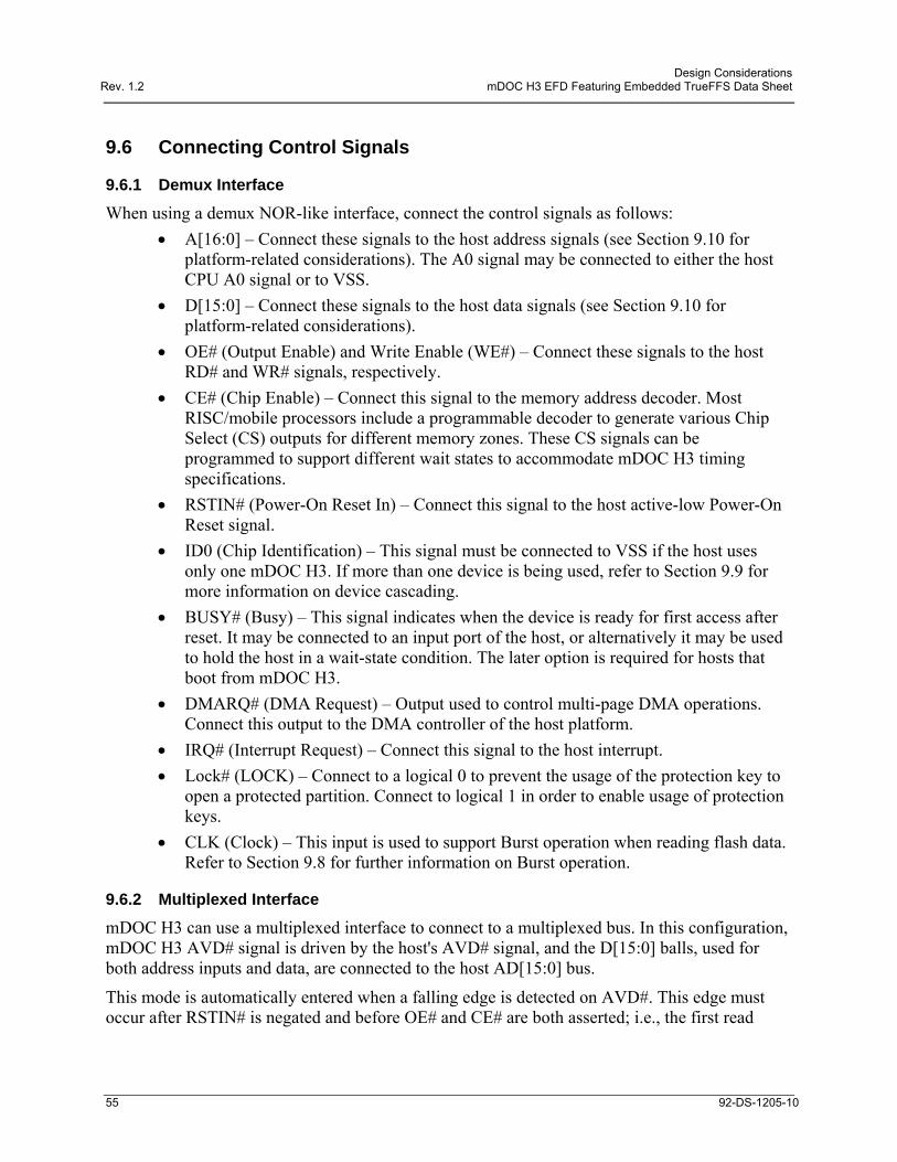
Rev. 1.2 Design Considerations
mDOC H3 EFD Featuring Embedded TrueFFS Data Sheet
55 92-DS-1205-10
9.6 Connecting Control Signals
9.6.1 Demux Interface
When using a demux NOR-like interface, connect the control signals as follows: • A[16:0] – Connect these signals to the host address signals (see Section 9.10 for
platform-related considerations). The A0 signal may be connected to either the host CPU A0 signal or to VSS.
• D[15:0] – Connect these signals to the host data signals (see Section 9.10 for platform-related considerations).
• OE# (Output Enable) and Write Enable (WE#) – Connect these signals to the host RD# and WR# signals, respectively.
• CE# (Chip Enable) – Connect this signal to the memory address decoder. Most RISC/mobile processors include a programmable decoder to generate various Chip Select (CS) outputs for different memory zones. These CS signals can be programmed to support different wait states to accommodate mDOC H3 timing specifications.
• RSTIN# (Power-On Reset In) – Connect this signal to the host active-low Power-On Reset signal.
• ID0 (Chip Identification) – This signal must be connected to VSS if the host uses only one mDOC H3. If more than one device is being used, refer to Section 9.9 for more information on device cascading.
• BUSY# (Busy) – This signal indicates when the device is ready for first access after reset. It may be connected to an input port of the host, or alternatively it may be used to hold the host in a wait-state condition. The later option is required for hosts that boot from mDOC H3.
• DMARQ# (DMA Request) – Output used to control multi-page DMA operations. Connect this output to the DMA controller of the host platform.
• IRQ# (Interrupt Request) – Connect this signal to the host interrupt. • Lock# (LOCK) – Connect to a logical 0 to prevent the usage of the protection key to
open a protected partition. Connect to logical 1 in order to enable usage of protection keys.
• CLK (Clock) – This input is used to support Burst operation when reading flash data. Refer to Section 9.8 for further information on Burst operation.
9.6.2 Multiplexed Interface
mDOC H3 can use a multiplexed interface to connect to a multiplexed bus. In this configuration, mDOC H3 AVD# signal is driven by the host's AVD# signal, and the D[15:0] balls, used for both address inputs and data, are connected to the host AD[15:0] bus.
This mode is automatically entered when a falling edge is detected on AVD#. This edge must occur after RSTIN# is negated and before OE# and CE# are both asserted; i.e., the first read

Rev. 1.2 Design Considerations
mDOC H3 EFD Featuring Embedded TrueFFS Data Sheet
56 92-DS-1205-10
cycle made to mDOC must observe the multiplexed mode protocol. See Section 10 for more information about the related timing requirements.
Please refer to Section 2.3 for ballout and signal descriptions, and to Section 10 for timing specifications for a multiplexed interface.
9.7 Implementing the Interrupt Mechanism
9.7.1 Hardware Configuration
To configure the hardware for working with the interrupt mechanism, the IRQ# ball should be connected to a host interrupt input.
9.7.2 Software Configuration
IRQ# signal may be used by mDOC H3 to interrupt the host system, provided that device interrupts are enabled. Interrupts can be enabled or disabled using the flHwConfig DOC Driver API. For more information see the DOC Driver 1.0 Block Device (BD) Software Developer Kit (SDK) Developer Guide. When asserted, the IRQ# signal will remain asserted until cleaned (level only). This cleaning is performed automatically by the DOC Driver as part of the API (read or write) completion.
mDOC H3 will interrupt the host system in the following cases: • Device is ready to receive a data block (excluding the first) during write operation. • When using DMA transfers: • On completion of block device operation to mDOC H3. • Device is ready to send a data block during a read operation.
9.8 DMA and Burst Operation mDOC H3 enhances performance using various proprietary techniques among them are
• Burst operation to read or write large chunks of data, providing a Burst speed. • DMA operation to release the CPU for other tasks in coordination with the platform’s
DMA controller. This is especially useful during the boot stage. Up to 128KB of data can be transferred during a DMA operation.
9.8.1 DMA Operation
mDOC H3 provides a DMARQ# output that enables data transfer using the host DMA controller. During DMA operation, the DMARQ# output is used to notify the host DMA controller that data is ready to be read or written. mDOC H3 protocol enables such data transfer up to the maximal size of 128KB per read or write operation.
The DMARQ# output sensitivity is selected by setting the EDGE bit in the DMA Control register:
1. Edge DMARQ# output pulses to indicate to the DMA controller that a data is ready to be transferred. The EDGE bit is set to 1 for this mode. The amount of data that will be transferred corresponds to data block size.

Rev. 1.2 Design Considerations
mDOC H3 EFD Featuring Embedded TrueFFS Data Sheet
57 92-DS-1205-10
2. Level DMARQ# output is asserted while the data is available for read, or data can be accepted for write. The EDGE bit is set to 0 for this mode.
The following steps are required in order to initiate a DMA operation:
1. If the DMA controller supports an edge-sensitive DMARQ# signal, then initialize the DMA controller to transfer 512 bytes (or your chosen data block size) upon each DMA request. If the DMA controller supports a level-sensitive DMARQ# signal, then initialize the DMA controller to transfer data continuously while DMARQ# is asserted.
2. Set in the DMA Control register values of EDGE bit, PULSE_WIDTH and DMA polarity corresponding to settings of the host DMA controller. This can be done only once after system power-up.
3. Enable DMA transfer with DMA_EN bit in the DMA control register.
4. If host DMA controller detects the de-assertion of the DMARQ# signal too late (and attempts to transfer additional words as a result), then DMARQ# can be configured to be de-asserted earlier by using the DMA Negation Register.
5. Program host DMA controller to transfer the same number of sectors as will be given in following logical command.
6. Issue the DMA data-transfer read/write command with same number of sectors to transfer as given in the previous step (prior to this, the device should be instructed to perform transfers in DMA-mode).
Upon command completion IRQ# will be asserted (it is recommended to use IRQ# when working with DMA). In case of a failure, less than expected amount of data could be transferred.
In commands that use DMA transfer, IRQ# is activated only at the completion of the whole command; while in commands that do not use DMA transfer IRQ# is typically activated with every data transfer.
Default setting of DMARQ# is level and active-low. It can be modified using the flHwConfig DOC Driver API. For more information see the DOC Driver 1.0 Block Device (BD) Software Developer Kit (SDK) Developer Guide..
9.8.2 Synchronous Burst Operation
In this mode the host reads full sections of 16-bit words synchronized to the CLK input.
Burst operation is controlled by 5 bit fields in each Burst Mode Control register (one for Burst read and one for Burst write): BURST_EN, WAIT_STATE, LATENCY, HOLD and LENGTH. For full details on this register, please refer to Section 7.
Burst Read / Write mode is enabled by setting the BURST_EN bit in each Burst Mode Control register.

Rev. 1.2 Design Considerations
mDOC H3 EFD Featuring Embedded TrueFFS Data Sheet
58 92-DS-1205-10
9.8.2.1 Read Mode
The LATENCY field controls the number of clock cycles between mDOC H3 sampling CE# being asserted and when the first word of data is available to be latched by the host. This number of clock cycles is equal to 3 + LATENCY.
WAIT_STATE allows setting the number of CLK after the host has read the last word until the release of the CE#.
• 1: One CLK clock before CE# release • 2: Two CLK clocks before CE# release • 3: Three CLK clocks before CE# release
The HOLD bit in the Burst Mode Control register can be set to hold each data word valid for two clock cycles rather than one.
Note: If HOLD = 1, then the data is available to be latched on this clock and on the subsequent clock.
The LENGTH field must be programmed with the length of the burst to be performed (0 corresponds to 4 cycles; 1 to 8 cycles, 2 to 16 and 3 corresponds to 32 cycles). Each burst cycle must read exactly this number of words.
The CLK input can be toggled continuously or can be halted. When halting the CLK input, the following guidelines must be observed:
• The host must provide a clock signal for the full sequence defined by the LATENCY, WAIT STATE, HOLD and LENGTH bit fields. The clock can only be stopped after the release of CE#.
• The clock can be halted momentarily during a burst sequence but the host must provide rising clock edges for the completion of the burst sequence.
Note: For full information regarding the Synchronous Burst Mode see the DOC Driver 1.0 Block Device (BD) Software Developer Kit (SDK) Developer Guide.
Figure 16: Demux Read Burst Mode

Rev. 1.2 Design Considerations
mDOC H3 EFD Featuring Embedded TrueFFS Data Sheet
59 92-DS-1205-10
Valid address D0 D1 D2 D3 D4 D5 D6 D7
Burst CLK
CE
OE
AVD
Data
Latency=1
Figure 17: Multiplexed Read Busrt Mode
Notes: 1. Note: AVD must be asserted on the following clock after the assertion of CE.
2. No collision should be allowed between the AVD and OE signal.
9.8.2.2 Write Mode The Write mode is similar to the Read mode with the following exceptions:
• WAIT_STATE = 0: 1 clock added. • WAIT_STATE = 1: 2 clocks added. • WAIT_STATE = 2: 3 clocks added. • WAIT_STATE = 3: 4 clocks added.
Figure 1818: Demux Write Burst Mode
Note: WE is sampled on the 1st clock after CE assertion. It must be active (low) for at least one clock cycle, after that the status of the WE signal is not important (Ø).

Rev. 1.2 Design Considerations
mDOC H3 EFD Featuring Embedded TrueFFS Data Sheet
60 92-DS-1205-10
Figure 19: Multiplexed Write Burst Mode
9.9 Device Cascading Up to two devices can be cascaded with no external decoding circuitry. Figure 19 illustrates the configuration required to cascade two devices on the host bus (only the relevant cascading signals are included in this figure, although all other signals must also be connected). All balls of the cascaded devices must be wired in common, except for ID0. The ID ball values determine the identity of each device – the first device is identified by connecting the ID ball as 0, and the second device by connecting the ID ball as 1. Systems that use only one mDOC H3 should connect ID0 to GND.
Figure 19: mDOC H3 Cascaded Configuration
ID0
CE#OE#WE#
CE#
WE# OE#
V SS
ID0
CE#OE#WE#
VCCQ
2nd1st

Rev. 1.2 Design Considerations
mDOC H3 EFD Featuring Embedded TrueFFS Data Sheet
61 92-DS-1205-10
9.10 Platform-Specific Issues This section discusses hardware design issues for major embedded RISC processor families.
9.10.1 Wait State
Wait states can be implemented only when mDOC H3 is designed in a bus that supports a Wait state insertion, and supplies a WAIT signal.
9.10.2 Big and Little Endian Systems
mDOC H3 is a Little Endian device. Therefore, byte lane 0 (D[7:0]) is its Least Significant Byte (LSB) and byte lane 1 (D[15:8]) is its Most Significant Byte (MSB). Within the byte lanes, bit D0 and bit D8 are the least significant bits of their respective byte lanes. mDOC H3 can be connected to a Big Endian device in one of two ways:
1. Make sure to identify byte lane 0 and byte lane 1 of your processor. Then, connect the data bus so that the byte lanes of the CPU match the byte lanes of mDOC H3. Pay special attention to processors that also change the bit ordering within the bytes (for example, PowerPC). Failing to follow these rules results in improper connection of mDOC H3, and prevents the DOC Driver from identifying it.
2. If needed, set the SWAP bits in the Endian Control register. This enables byte swapping when used with big endian 16-bit hosts.
9.10.3 Busy Signal
The Busy signal (BUSY#) indicates that mDOC H3 has not yet completed internal initialization. After reset, BUSY# is asserted while the IPL is downloaded into the internal boot block. Once the download process is completed, BUSY# is de-asserted. It can be used to delay the first access to mDOC H3 until it is ready to accept valid cycles.
Note: mDOC H3 does NOT use this signal to indicate that the flash is in busy state (e.g. program, read, or erase).
9.10.4 Working with 16/32-Bit Systems
mDOC H3 uses a 16-bit data bus and supports 16-bit data access by default. However, it can be configured to support 32-bit data access mode. This section describes the connections required for each mode.
The default of the DOC Driver for mDOC H3 is set to work in 16-bit mode. It must be specially configured to support 32-bit mode. Please see DOC Driver or TrueFFS 7.1 documentation for further details.
Note: The mDOC H3 data bus must be connected to the Least Significant Bits (LSB) of the system.
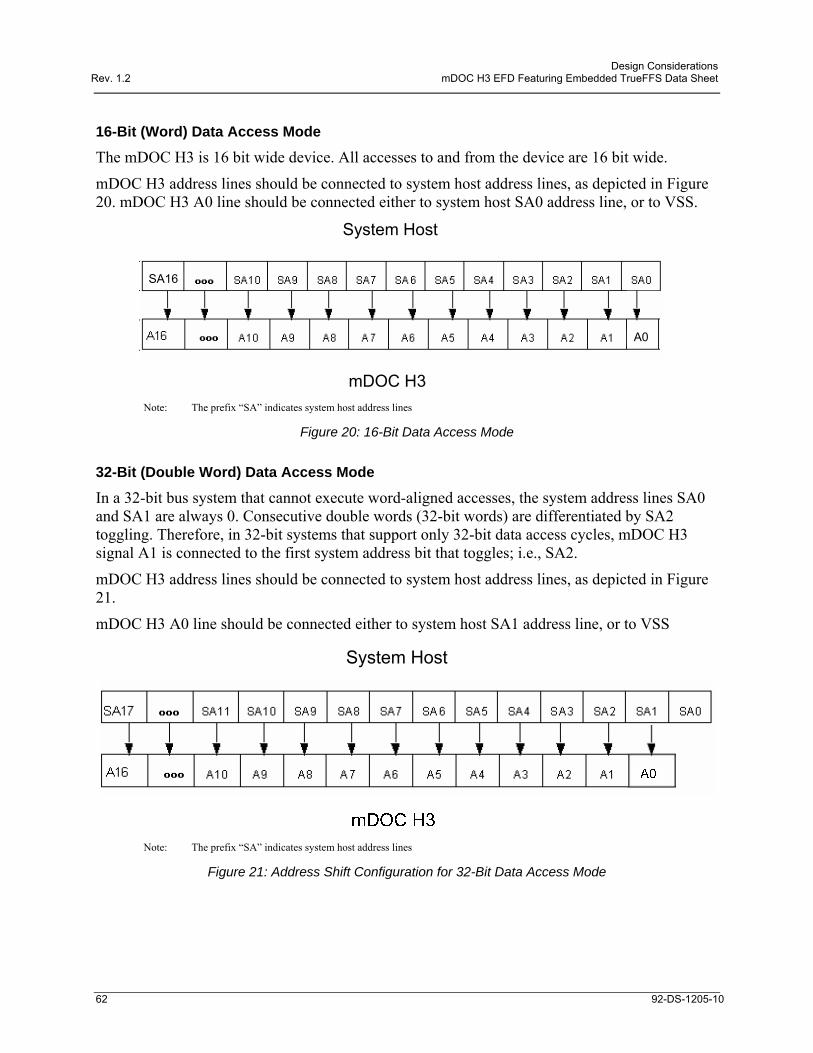
Rev. 1.2 Design Considerations
mDOC H3 EFD Featuring Embedded TrueFFS Data Sheet
62 92-DS-1205-10
16-Bit (Word) Data Access Mode
The mDOC H3 is 16 bit wide device. All accesses to and from the device are 16 bit wide.
mDOC H3 address lines should be connected to system host address lines, as depicted in Figure 20. mDOC H3 A0 line should be connected either to system host SA0 address line, or to VSS.
System Host
mDOC H3
SA16
A0
Note: The prefix “SA” indicates system host address lines
Figure 20: 16-Bit Data Access Mode
32-Bit (Double Word) Data Access Mode
In a 32-bit bus system that cannot execute word-aligned accesses, the system address lines SA0 and SA1 are always 0. Consecutive double words (32-bit words) are differentiated by SA2 toggling. Therefore, in 32-bit systems that support only 32-bit data access cycles, mDOC H3 signal A1 is connected to the first system address bit that toggles; i.e., SA2.
mDOC H3 address lines should be connected to system host address lines, as depicted in Figure 21.
mDOC H3 A0 line should be connected either to system host SA1 address line, or to VSS
System Host
Note: The prefix “SA” indicates system host address lines
Figure 21: Address Shift Configuration for 32-Bit Data Access Mode

Rev. 1.2 Design Considerations
mDOC H3 EFD Featuring Embedded TrueFFS Data Sheet
63 92-DS-1205-10
9.11 Design Environment mDOC H3 provides a complete design environment consisting of:
• Evaluation boards (EVBs) for enabling software integration and development with mDOC H3, even before the target platform is available.
• Programming solutions: • Programmer
o Programming house
o On-board programming
o DOC Driver Software Development Kit (SDK) • TrueFFs 7.1 Software Development Kit (SDK) • XP utilities:
o DFormat
o DImage
o DInfo • Documentation:
o Data sheet
o Application notes
o Technical notes
o Articles
o White papers
Please visit the SanDisk website (www.sandisk.com) for the most updated documentation.

Rev. 1.2 Product Specifications
mDOC H3 EFD Featuring Embedded TrueFFS Data Sheet
64 92-DS-1205-10
10. PRODUCT SPECIFICATIONS
10.1 Environmental Specifications
10.1.1 Operating Temperature Table 5: Operating Temperature
Product Ordering Info Temperature Range MD2534-XXX-YY -40°C to +85°C SDE-ZZ-XXXY-BBB -25°C to +85°C
10.1.2 Thermal Characteristics Table 6: Thermal Characteristics
Thermal Resistance (°C/W) Junction to Case (θJC): 40 Junction to Ambient (θJA): 90
10.1.3 Humidity
10% to 90% relative, non-condensing.
10.2 Electrical Specifications
10.2.1 Absolute Maximum Ratings Table 7: Absolute Maximum Ratings
Parameter Symbol Rating Units 1.8V DC supply voltage VCC1 -0.3 to 2 V 3.3V DC supply voltage VCC2 -0.3 to 4 V 1.8/3.3V DC supply voltage VCCQ -0.3 to 4 V 1.8/3.3V DC supply voltage VCC -0.3 to 4 V Maximum duration of applying only part of the power supplies (some of the power supply ON and the other OFF)
T1supply 500 msec
Input pin voltage Vin -0.3 to 3.6 V Ambient Temperature OTR -25* to 85 °C Storage temperature Tstg -55 to +125 °C
* For MD2534-XXX-YY products the value is -40oC
Notes: 1. Permanent device damage may occur if absolute maximum ratings are exceeded. Exposure to absolute maximum rating conditions for extended periods may affect device reliability.

Rev. 1.2 Product Specifications
mDOC H3 EFD Featuring Embedded TrueFFS Data Sheet
65 92-DS-1205-10
2. When operating mDOC H3 with separate power supplies for VCCQ/VCC/VCC1/VCC2, it is recommended to turn the supplies on and off simultaneously. Providing power separately (either at power-on or power-off) can cause excessive power dissipation. Damage to the device may result if this condition persists for more than 500 msec.
10.2.2 Capacitance Table 8: Capacitance
Symbol Parameter Conditions Min Typ Max Unit C
IN Input capacitance V
IN = 0V 10 pF
COUT
Output capacitance VO = 0V 10 pF
10.2.3 DC Characteristics
10.2.3.1 1.8V Core, 1.8V I/O
Table 9: 1.8V Core, 1.8V I/O
Symbol Parameter Conditions Min Typ Max Unit VCCQ I/O power supply 1.65 1.8 1.95 V VCC2 Internal supply NC NC NC - VCC Device supply 1.65 1.8 1.95 V VCC1 Internal supply 1.65 1.8 1.95 V VIH Input High-level Voltage 0.65*
VCCQ 0.3+
VCCQ V
VIL Input Low-level Voltage -0.3 0.35* VCCQ
V
II Input Leakage Current 0≤VIN≤VCCQ -10 10 uA IOZ Tri-State output leakage current 0≤VIN≤VCCQ -10 10 uA
Vhys Hysteresis Schmidt trigger inputs
400 mV
VOH High-level Output Voltage IOH=4mA-12mA
VCCQ-0.45
V
VOL Low-level Output Voltage IOH=4mA-12mA
0.45 V
PU Pull up resistance 95 149 261 kΩ PD Pull down resistance 77 135 312 kΩ
Turbo mode 30 75
Icc Active supply current1
Power Save mode
20 65
mA
Standby mode 5 10 mA ICCS
Standby supply current1
DPD mode 75 130 uA
Note: Sum of all current on VCC, VCCQ and VCC1 balls. CL = 0 pF. T=25C.

Rev. 1.2 Product Specifications
mDOC H3 EFD Featuring Embedded TrueFFS Data Sheet
66 92-DS-1205-10
10.2.3.2 3.3V Core, 1.8V I/O
Table 10: 3.3V Core, 1.8V I/O
Symbol Parameter Conditions Min Typ Max Unit VCCQ I/O power supply 1.65 1.8 1.95 V VCC2 Internal supply 2.7 3.3 3.6 V VCC Device supply 2.7 3.3 3.6 V
VCC1 Internal supply NC NC NC -
VIH Input High-level Voltage 0.65* VCCQ
0.3+ VCCQ
V
VIL Input Low-level Voltage -0.3 0.35* VCCQ
V
II Input Leakage Current 0≤VIN≤VCCQ -10 10 uA IOZ Tri-State output leakage current 0≤VIN≤VCCQ -10 10 uA
Vhys Hysteresis Schmidt trigger inputs
400 mV
VOH High-level Output Voltage IOH=4mA-12mA
VCCQ-0.45
V
VOL Low-level Output Voltage IOH=4mA-12mA
0.45 V
PU Pull up resistance 95 149 261 kΩ PD Pull down resistance 77 135 312 kΩ
Turbo mode 30 60 Icc3
Active supply current1 Power Save
mode
20 40
mA
Standby mode 5 10 mA
ICCS3
Standby supply current1
DPD mode 60 130 uA
Notes: 1. Sum of all current on VCC, VCCQ and VCC2 balls. CL = 0 pF. T=25C.
2. For all products with ordering info SDE-ZZ-XXXY-BBB, Icc and Iccs parameters are estimations.

Rev. 1.2 Product Specifications
mDOC H3 EFD Featuring Embedded TrueFFS Data Sheet
67 92-DS-1205-10
10.2.3.3 3.3V Core, 3.3V I/O
Table 11: 3.3V Core, 3.3V I/O
Symbol Parameter Conditions Min Typ Max Unit VCCQ I/O power supply 2.7 3.3 3.6 V VCC2 Internal supply 2.7 3.3 3.6 V VCC Device supply 2.7 3.3 3.6 V
VCC1 Internal supply NC NC NC - VIH Input High-level Voltage 2.0 3.6 V VIL Input Low-level Voltage -0.3 0.8 V II Input Leakage Current 0≤VIN≤VCCQ -10 10 uA
IOZ Tri-State output leakage current 0≤VIN≤VCCQ -10 10 uA Vhys Hysteresis Schmidt
trigger inputs 520 mV
VOH High-level Output Voltage IOH=4mA-12mA
2.4 V
VOL Low-level Output Voltage IOH=4mA-12mA
0.4 V
PU Pull up resistance 50 65 100 kΩ PD Pull down resistance 40 56 107 kΩ
Turbo mode 30 60 Icc
Active supply current1 (cycle time = 60 ns) Power Save
mode
20 402
mA
Standby mode 5 10 mA ICCS
Standby supply current1
DPD mode
110
150
uA
Note: Sum of all current on VCC, VCCQ and VCC2 balls. CL = 0 pF. T=25C.

Rev. 1.2 Product Specifications
mDOC H3 EFD Featuring Embedded TrueFFS Data Sheet
68 92-DS-1205-10
10.3 Timing Specifications
10.3.1 Operating Conditions
Timing specifications are based on the conditions defined in Table 12. Table 12: Operating Conditions
Parameter 1.8V 3.3V Ambient temperature (TA) -40°C to +85°C -40°C to +85°C Supply Voltage (VCCQ) 1.65V – 1.95V 2.7V – 3.6V
CLK, SCS#, SI, SO, SCLK 3ns 3ns
Input fall and rise time (10%-90% VCCQ)
All other inputs 5ns 5ns
Input timing level VCCQ/2 VCCQ/2 Output timing level VCCQ/2 VCCQ/2 Output Load Push/Pull outputs
30pF 30pF
Note: Max input fall and rise is 100ns.

Rev. 1.2 Product Specifications
mDOC H3 EFD Featuring Embedded TrueFFS Data Sheet
69 92-DS-1205-10
10.3.2 Demux Asynchronous Read Timing
Figure 22: Demux Asynchronous Read Timing
A0 A1
D0 D1 Tacc (ipl_ram)
Tacc (ipl_ram) Tdh
Tsua
CE OE
Address
Data
Figure 23: Demux Read Timing – Asynchronous Boot Mode
Table 13: Demux Asynchronous Read Timing Parameters
Symbol 1.8V 3.3V Description Min Max Min Max
Units
Tsua Address setup time (Figure 22) 1 1 ns
Tsua Address setup time (Figure 23) – Asynchronous boot mode -2 -2 ns
Tacc(async) Asynchronous access time (Registers) 18 15 ns
Tacc(ipl_ram) RAM access time 25 22 ns Tdh Data hold time 1.5 10 1.5 10 ns Tah Address hold time 0 0 ns Tw(ceh) CE# high pulse width 10 10 ns Tw(cel) CE# low pulse width 20 15 ns Tw(oeh) OE# high pulse width 10 10 ns Tw(oel) OE# low pulse width 20 15 ns
Note: Tw(cel) must be greater than or equal to Tw(oel).CE# falling edge should together with or before OE# falling edge, not after.

Rev. 1.2 Product Specifications
mDOC H3 EFD Featuring Embedded TrueFFS Data Sheet
70 92-DS-1205-10
10.3.3 Demux Asynchronous Write Timing
Figure 24: Demux Asynchronous Write Timing
Table 14: Demux Asynchronous Write Timing Parameters
1.8V 3.3V Symbol Description Min Max Min Max
Units
Tasu Address setup 1 1.2 ns Tah Address hold time 3 3 ns Tdsu Data setup 11 11 ns Tdh Data hold 0 0 ns Tw(ceh) CE# high pulse width 10 10 ns Tw(cel) CE# low pulse width 15 15 ns Tw(weh) WE# high pulse width 10 10 ns Tw(wel) WE# low pulse width 15 15 ns
Note: Tw(cel) must be greater than or equal to Tw(wel).
10.3.4 Multiplexed Asynchronous Read Timing
Address valid D0Tacc Tdh
TahTasu
TavdoeTavdTavd
Tw (oeh)Tw (oeh)Tw (oel)Tw (oel)
CE
OE
AVD
Data Figure 25: Multiplexed Asynchronous Read Timing Diagram

Rev. 1.2 Product Specifications
mDOC H3 EFD Featuring Embedded TrueFFS Data Sheet
71 92-DS-1205-10
A0 D0Tdh Tdsu
Tah Tasu
TavdweTavd Tavd
Tw(weh)Tw(wel) Tw(weh)Tw(wel)
CE
WE
AVD
Data
Table 15: Multiplexed Asynchronous Read Timing Parameters
1.8V 3.3V Symbol Description Min Max Min Max
Units
Tasu Address setup 3 2 ns Tah Address hold 5 5 ns Taccs Access time 15 13 ns Tdh Data hold 1.5 1.4 ns Tavd AVD# pulse width 6 6 ns Tw(oel) OE# low pulse width 15 15 ns Tw(oeh) OE# high pulse width 10 10 ns Tavdoe AVD rising to OE falling 6 6 ns
10.3.5 Multiplexed Asynchronous Write Timing
Figure 26: Multiplexed Asynchronous Write Timing Diagram
Table 16:
Multiplexed
Asynchronous Write Timing Parameters
1.8V 3.3V Symbol Description Min Max Min Max
Units
Tasu Address setup 3 2 ns Tah Address hold 5 5 ns Tdsu Data setup time 12 11 ns Tdh Data hold 0 0 ns Tavd AVD# pulse width 6 6 ns
Tw(wel)
WE# low pulse width WE# should be negated before or together with CE#
15 15
ns
Tw(weh) WE# high pulse width 5 5 ns Tavdwe AVD rising to WE falling 1 1 ns

Rev. 1.2 Product Specifications
mDOC H3 EFD Featuring Embedded TrueFFS Data Sheet
72 92-DS-1205-10
10.3.6 Demux Burst Read Timing
Figure 27: Demux Burst Read Timing Diagram
Table 17: Demux Burst Read Timing Parameters
1.8V 3.3V
Symbol Description Min Max Min Max Units
Tasu Address setup 4 4 ns Tah Address hold 2.5 2.5 ns Tcesu CE# setup 9 9 ns Tacc Access time 11.2 8.1 ns Tcyc Burst clock cycle time 14 11 ns Tdh Data hold time 2 2 ns
Notes: 1. All timing specifications are with reference to the rising edge of the Burst clock (CLK signal).
2. Shown with the following Burst Mode Control Register (Read) parameters:
• HOLD = 0 • LENGTH = 8 • LATENCY = 0 • WAIT_STATE = 0 3. This diagram is applicable only if working with continuous clock.
4. Burst clock cycle time (Tcyc) values are specified for Turbo mode. While in Power-Save mode, clock cycle time should be doubled.

Rev. 1.2 Product Specifications
mDOC H3 EFD Featuring Embedded TrueFFS Data Sheet
73 92-DS-1205-10
10.3.7 Demux Burst Write Timing
A0
D0 D1 D2 D3
TdhTdsu
TwehTwesu
TahTasu
Tcesu
TcycTcycBurst CLK
CE
Address
WE
Data Figure 28: Demux Burst Write Timing Diagram
Table 18: Demux Burst Write Timing Parameters
1.8V 3.3V Symbol Description Min Max Min Max
Units
Tasu Address setup 4 4 ns Tah Address hold 2.5 2.5 ns Tcesu CE# setup 7 7 ns Twesu WE# setup time 4 4 ns Tweh WE# hold time 5 5 ns Tcyc Burst clock cycle time 12.5 12.5 ns Tdsu Data setup time 4 4 ns Tdh Data hold time 2.5 2.5 ns
Notes: 1. All timing specifications are with reference to the rising edge of the Burst clock (CLK signal).
2. Shown with the following Burst Mode Control Register (Read) parameters:
• HOLD = 0 • LENGTH = 8 • LATENCY = 0 • WAIT_STATE = 0 3. This diagram is applicable only if working with continuous clock.
4. Burst clock cycle time (Tcyc) values are specified for Turbo mode. While in Power-Save mode, clock cycle time should be doubled.

Rev. 1.2 Product Specifications
mDOC H3 EFD Featuring Embedded TrueFFS Data Sheet
74 92-DS-1205-10
10.3.8 Multiplexed Burst Read Timing
Valid address D0 D1 D2 D3 D4 D5 D6 D7
TaccTdhTah
Tasu
TavdhTavdsu
Tcesu
TcycTcycBurst CLK
CE
OE
AVD
Data
Figure 29: Multiplexed Burst Read Timing Diagram
Table 19: Multiplexed Burst Read Timing Parameters
1.8V 3.3V
Symbol Description Min Max Min Max Units
Tasu Address setup 4 4 ns Tah Address hold 2.5 2.5 ns Tcesu CE setup 9 9 ns Tacc Access time 11 8 ns Tcyc Burst clock cycle time 12.5 12.5 ns Tdh Data hold time 2 2 ns Tavdsu AVD setup time 7 7 ns Tavdh AVD hold time 1 1 ns
Notes: 1. All timing specifications are with reference to the rising edge of the Burst clock (CLK signal).
2. Shown with the following Burst Mode Control Register (Read) parameters:
• HOLD = 0 • LENGTH = 8 • LATENCY = 1 • WAIT_STATE = 0 3. Burst clock cycle time (Tcyc) values are specified for Turbo mode. While in Power-
Save mode, clock cycle time should be double.

Rev. 1.2 Product Specifications
mDOC H3 EFD Featuring Embedded TrueFFS Data Sheet
75 92-DS-1205-10
10.3.9 DMA Request Timing Diagram
10.3.9.1 Asynchronous Data Transfer
Table 20 lists DMA request timing parameters and Figure 30 shows the DMA request timing diagram in Asynchronous data transfer.
Tp(ce/oe)Tw(dmarq)Tw(dmarq)
CE/OE
DMARQ#
Figure 30: DMA Request Timing Diagram (Asynchronous Data Transfer)
Table 20: DMA Request Timing Parameters (Asynchronous Data Transfer)
1.8V 3.3V Symbol Description Min Max Min Max
Units
Tw(dmarq) DMARQ# pulse width1 20 20 ns
Tp(ce/oe) CE/OE to DMARQ# negation2 19 16 ns
Notes: 1. Applies to EDGE mode only. The DMARQ# pulse width can be configured by SW.
2. Applies to LEVEL mode only. Values refer to rising of CE or OE signal, which ever negated first.
10.3.9.2 Synchronous Data Transfer
Table 21 lists DMA request timing parameters and Figure 31 shows the DMA request timing diagram in Synchronous data transfer.
Tp (b c lk)Tw ( d mar q )Tw ( d mar q )
B CL K
DMA RQ #
CLK
Figure 31: DMA request Timing Diagram (Synchronous Data Transfer)
Table 21: DMA Request Timing Parameters (Synchronous Data Transfer)
1.8V 3.3V Symbol Description Min Max Min Max
Units
Tw(dmarq) DMARQ# pulse width1 20 20 ns Tp(bclk) CLK to DMARQ# negation2 17 13 ns
Notes: 1. Applies to EDGE mode only. The DMARQ# pulse width can be configured by SW. Timing is relative to the rising edge of CLK which samples CE# asserted.
2. Applies to LEVEL mode only.

Rev. 1.2 Product Specifications
mDOC H3 EFD Featuring Embedded TrueFFS Data Sheet
76 92-DS-1205-10
10.3.10 SPI Timing
Table 22 lists SPI slave timing parameters. Figure 32 and Figure 33 show the SPI slave timing diagram.
Table 22: Slave SPI Timing Parameters
Symbol 1.8V 3.3V
Description Min Max Min Max
Units Notes
tw(SCLK1) SCLK high pulse width 15 15 ns tw(SCLK0) SCLK low pulse width 15 15 ns tcyc(SCLK) SCLK period 40 40 ns tsu(SI) SI to SCLK setup 8 8 ns tho(SI) SCLK to SI hold 8 8 ns tsu(SCS#) SCS# to SCLK setup 8 8 ns tho(SCS#) SCLK to SCS# hold 16 16 ns tw(SCS#1) SCS# high pulse width 16 16 ns tp(SO1) SCLK to SO delay 22 17 ns tp(SO0) SCLK to SO delay 22 16 ns thiz(SO) SCS# to SO Hi-Z 12 10 ns
tHIZ(SO)tp(SI0)tp(SI1)
tHO(SI)
tSU(SI)
tw(SCS#1)tw(SCS#1)
tw(SCLK1)tw(SCLK1)tw(SCLK0)tw(SCLK0)
tw(SCLK0)
tcyc(SCLK)
tw(SCLK0)tw(SCLK1)tw(SCLK1)
tcyc(SCLK)
SCLK (mode 0,3)
SCLK (mode 1,2)
SCS#
SI
SO Figure 32: Slave SPI Data Timing

Rev. 1.2 Product Specifications
mDOC H3 EFD Featuring Embedded TrueFFS Data Sheet
77 92-DS-1205-10
Figure 33: Slave SPI Control Timing
10.3.11 Power Supply Sequence
When operating mDOC H3 with separate power supplies powering the VCCQ, VCC, VCC1 or VCC2 rails, it is desirable to turn the supplies on and off simultaneously. Providing power to one supply rail and not the other (either at power-on or power-off) can cause excessive power dissipation. Damage to the device may result if this condition persists for more than 500 msec.
10.3.12 Power-Up Timing
mDOC H3 is reset by assertion of the RSTIN# input. When this signal is negated, mDOC H3 initiates a download procedure from the flash memory into the internal Programmable Boot Block. During this procedure, mDOC H3 does not respond to read or write access.
Host systems must therefore observe the requirements described below for initial access to mDOC H3. Any of the following methods may be employed to guarantee first-access timing requirements:
• Use a software loop to wait at least Tp (BUSY1) before accessing the device after the reset signal is negated.
• Poll the state of the BUSY# output.
• Use the BUSY# output to hold the host CPU in wait state before initiating the first access which will be a RAM read cycle. At least one of the signals CE# and OE# must be kept negated (high) until BUSY# is negated.
Hosts that use mDOC H3 to boot the system must employ the latter option or use another method to guarantee the required timing of initial access.

Rev. 1.2 Product Specifications
mDOC H3 EFD Featuring Embedded TrueFFS Data Sheet
78 92-DS-1205-10
Table 23: Power-Up Timing Parameters
Symbol Description Min Max Units TREC (VCC-RSTIN) VCC/VCCQ stable to RSTIN# 1 500 μs
TW (RSTIN) RSTIN# asserted pulse width 50 ns
TP (BUSY0) RSTIN# to BUSY# 50 ns
TP (BUSY1) RSTIN# to BUSY# 3 75 ms
TP (VCC-BUSY0) VCC/VCCQ stable to BUSY# 500 μs
Tsu (RSTIN-AVD) RSTIN# to AVD# 2 3 μs
Tsu (BUSY-CE) BUSY# to CE# 0 μs
Trise (RSTIN) RSTIN# rise time 20 ns
Notes: 1. Specified from the final positive crossing of VCC/VCC1/VCC2/VCCQ minimum voltages.
2. Applies to multiplexed interface only.
3. TP (BUSY1) depends on IPL mode (Normal / Paged ) and device capacity. For unformatted devices this time may be up to one second.
Figure 34: Reset Timing

Rev. 1.2 Product Specifications
mDOC H3 EFD Featuring Embedded TrueFFS Data Sheet
79 92-DS-1205-10
10.4 Mechanical Dimensions
10.4.1 mDOC H3 1Gb (128MB)/2Gb (256MB)
FBGA 128MB (1Gb) dimensions: 9.0 ±0.1 mm x 12.0 ±0.1 mm x 1.1 ±0.1 mm
Ball pitch: 0.8 mm
9.0
12.0
1.1±0.1
0.26±0.04 0.80.4
0.4
0.9
0.8
1 2 3 4 5 6 7 8 9 10
0.46
±0.0
5
Top Side Bottom
A
B
C
D
E
F
G
H
J
K
L
M
N
P
0.8
0.20 S A
0.20
S B
0.10
S
0.10
S
Ø0.
06 M
S A
B
0.154X
INDEX
b
Figure 35: Mechanical Dimensions 9x12 FBGA Package
Dimensions in mm Symbol Ordering info
Min Nom Max
b MD2534-d2G-X-P 0.41 0.46 0.51
b SDED7-256M-N9 0.30 0.35 0.40

Rev. 1.2 Product Specifications
mDOC H3 EFD Featuring Embedded TrueFFS Data Sheet
80 92-DS-1205-10
10.4.2 mDOC H3 4Gb (512MB)/8Gb (1GB)
FBGA dimensions: 10.0 ±0.1 mm x 14.0 ±0.1 mm x 1.1 ±0.1 mm
Ball pitch: 0.8 mm
10±0.1
14±0
.1
1.1±0.1
0.23±0.050.4
0.4
0.8
1.4
1.8
1 2 3 4 5 6 7 8 9 10
0.35
±0.0
5
Top Side Bottom
INDEX
A
B
C
D
E
F
G
H
J
K
L
M
N
P
0.8
Figure 36: Mechanical Dimensions 10x14 FBGA Package

Rev. 1.2 Product Specifications
mDOC H3 EFD Featuring Embedded TrueFFS Data Sheet
81 92-DS-1205-10
10.4.3 mDOC H3 8Gb (1GB)/ 16Gb (2GB)/ 32Gb (4GB) / 64Gb (8GB)
FBGA dimensions: 12.0 ±0.1 mm x 18.0 ±0.1 mm x 1.3 ±0.1 mm
Ball pitch: 0.8 mm
Symbol Ordering Info Max Height(mm)
h SDED7-001G-NT 1.4
h SDED7-002G-NT 1.4
h SDED5-002G-NC 1.2
h SDED5-004G-NC 1.2
h SDED5-008G-NC 1.4
Figure 37: Mechanical Dimensions 12x18 FBGA Package

Rev. 1.2 Ordering Information
mDOC H3 EFD Featuring Embedded TrueFFS Data Sheet
82 92-DS-1205-10
11. ORDERING INFORMATION See Table 24 for mDOC H3 devices available and the associated order information. Table 24: mDOC H3 Ordering Information
Capacity Ordering Code MB Mb
Package Temperature Range
MD2534-d1G-X-P MD2534-d1G-X-P/Y
128 1024 (1Gbit)
9x12x1.2 BGA 115
balls
-40°C to +85°C
MD2534-d2G-X-P MD2534-d2G-X-P/Y
256 2048 (2Gbit)
9x12x1.2 BGA 115
balls
-40°C to +85°C
SDED7-256M-N9T SDED7-256M-N9Y
256 2048 (2Gbit)
9x12x1.2 BGA 115
balls
-25°C to +85°C
SDED7-512M-NAT SDED7-512M-NAY
512 4096 (4Gbit)
10x14x1.2 BGA 115
balls
-25°C to +85°C
MD2533-d8G-X-P MD2533-d8G-X-P/Y
1024 (1GB)
8192 (8Gbit)
12x18x1.4 BGA 115
balls
-40°C to +85°C
SDED5-001G-NAT SDED5-001G-NAY
1024 (1GB)
8192 (8Gbit)
10x14x1.2 BGA 115
balls
-25°C to +85°C
MD2533-d16G-X-P MD2533-d16G-X-P/Y
2048 (2GB)
16384 (16Gbit)
12x18x1.4 BGA 115
balls
-40°C to +85°C
SDED5-002G-NCT SDED5-002G-NCY
2048 (2GB)
16384 (16Gbit)
12x18x1.2 BGA 115
balls
-25°C to +85°C
SDED5-004G-NCT SDED5-004G-NCY
4096 (4GB)
32768 (32Gbit)
12x18x1.2 BGA 115
balls
-25°C to +85°C
SDED5-008G-NCT SDED5-008G-NCY
8192 (8GB)
65536 (64Gbit)
12x18x1.4 BGA 115
balls
-25°C to +85°C
Notes: 1. SDE Product Codes: T suffix specifies shipment in Tape & Reel; Y suffix specifies shipment in trays.
2. MD Product Codes:: Y suffix specifies shipment in trays; if not specified, shipment is in Tape & Reel

Rev. 1.2 Markings
mDOC H3 EFD Featuring Embedded TrueFFS Data Sheet
83 92-DS-1205-10
12. MARKINGS
12.1 mDOC H3 1Gb (128MB)/2Gb (256MB) Markings for MD2533-d1G XXX and MD2533-d26G XXX products:
First row: Logo
Second row: Product name
Third row: Ordering information
Fourth row: Production information:
yyww - Year and week
xx - Product status: Engineering samples “-ES”, Customer samples “-CS”
Forth row: ddddddd - Internal marking
Figure 38: MD2534-d1G-X-P Product Marking

Rev. 1.2 Markings
mDOC H3 EFD Featuring Embedded TrueFFS Data Sheet
84 92-DS-1205-10
12.2 mDOC H3 8Gb (1GB)/16Gb (2GB) Markings for MD2533-d8G XXX and MD2533-d16G XXX products:
First row: Product name
Second row: Logo
Third row: Ordering information
Fourth row: Production information:
yyww - Year and week
xxx - Product status: Engineering samples “-ES”, Customer samples “-CS”
Forth row: ddddddd - Internal marking
Figure 39: MD2533-d8G-X-P Product Marking

Rev. 1.2 Markings
mDOC H3 EFD Featuring Embedded TrueFFS Data Sheet
85 92-DS-1205-10
12.3 mDOC H3 2Gb (256MB)/ 4Gb (512MB)/ 8Gb (1GB)/ 16Gb (2GB)/ 32Gb (4GB) / 64Gb (8GB)
All products with ordering info of SDE-ZZ-XXXY-BBB will have following marking:
First row: Logo
Second row: VYWWXXXXN
V-Internal use
Y-year
WW-work week
XXXX – Internal use
N-Internal use
Third row: Ordering information
Fourth row: Internal use
Fifth row: country of origin i.e ‘TAIWAN’ or ‘CHINA’
XX is ‘ES’ or ‘CS’. There will be no XX marking for products in mass production.
Figure 40: Example of SDED7-512M-NA Product Marking

Rev. 1.2 Disclaimer of Liability
mDOC H3 EFD Featuring Embedded TrueFFS Data Sheet
86 92-DS-1205-10
DISCLAIMER OF LIABILITY SanDisk IL Ltd.’s general policy does not recommend the use of its products in life support applications wherein a failure or malfunction of the product may directly threaten life or injury. Accordingly, in any use of products in life support systems or other applications where failure could cause damage, injury or loss of life, the products should only be incorporated in systems designed with appropriate redundancy, fault tolerant or back-up features.
SanDisk IL shall not be liable for any loss, injury or damage caused by use of the Products in any of the following applications:
Special applications such as military related equipment, nuclear reactor control, and aerospace
Control devices for automotive vehicles, train, ship and traffic equipment
Safety system for disaster prevention and crime prevention
Medical-related equipment including medical measurement device.

Rev. 1.2 mDOC H3 EFD Featuring Embedded TrueFFS Data Sheet
87 92-DS-1205-10
HOW TO CONTACT US USA SanDisk Corporation, Corporate Headquarters. 601 McCarthy Blvd Milpitas, CA 95035 Phone: +1-408-801-1000 Fax: +1-408-801-8657
China SanDisk China Ltd. Room 121-122 Bldg. 2, International Commerce & Exhibition Ctr. Hong Hua Rd. Futian Free Trade Zone Shenzhen, China Phone: +86-755-8348-5218 Fax: +86-755-8348-5418
Europe SanDisk IL Ltd. 7 Atir Yeda St. Kfar Saba 44425, Israel Tel: +972-9-764-5000 Fax: +972-3-548-8666
Internet Sandisk.com/oem
General Information [email protected]
Japan SanDisk Japan Inc. Asahi Seimei Gotanda Bldg., 3F 5-25-16 Higashi-Gotanda Shinagawa-ku Tokyo, 141-0022 Phone: +81-3-5423-8101 Fax: +81-3-5423-8102
Taiwan SanDisk Asia Ltd. 14 F, No. 6, Sec. 3 Minquan East Road Taipei, Taiwan, 104 Tel: +886-2-2515-2522 Fax: +886-2-2515-2295 Sales and Technical Information
This document is for information use only and is subject to change without prior notice.
SanDisk IL Ltd assumes no responsibility for any errors that may appear in this document, nor for incidental or consequential damages resulting from the furnishing, performance or use of this material.
SanDisk IL’s products are not warranted to operate without failure. SanDisk IL’s general policy does not recommend the use of its products in life support applications where a failure or malfunction of the product could cause injury or loss of life. Per SanDisk IL’s Terms and Conditions of Sale, the user of SanDisk IL’s products in life support applications assumes all risk of such use and indemnifies SanDisk IL against all damages. See “Disclaimer of Liability". Accordingly, in any use of the Product in life support systems or other applications where failure could cause injury or loss of life, the Product should only be incorporated in systems designed with appropriate and sufficient redundancy or backup features.
All parts of the SanDisk IL’s documentation are protected by copyright law and all rights reserved.
Contact your local SanDisk sales office or distributor, or visit our website at www.sandisk.com to obtain the latest specifications before placing your order.
© 2007 SanDisk IL Ltd. All rights reserved.
TrueFFS, SanDisk and SanDisk logo are registered trademarks of SanDisk IL Ltd. and SanDisk Corporation, respectively. Other product names or service marks mentioned herein may be trademarks or registered trademarks of their respective owners and are hereby acknowledged.