data sheet - reedholm...
TRANSCRIPT
DS10056 03/01/2017 Page 1 of 14 Tel: 1.512.876.2268 e-mail: [email protected]
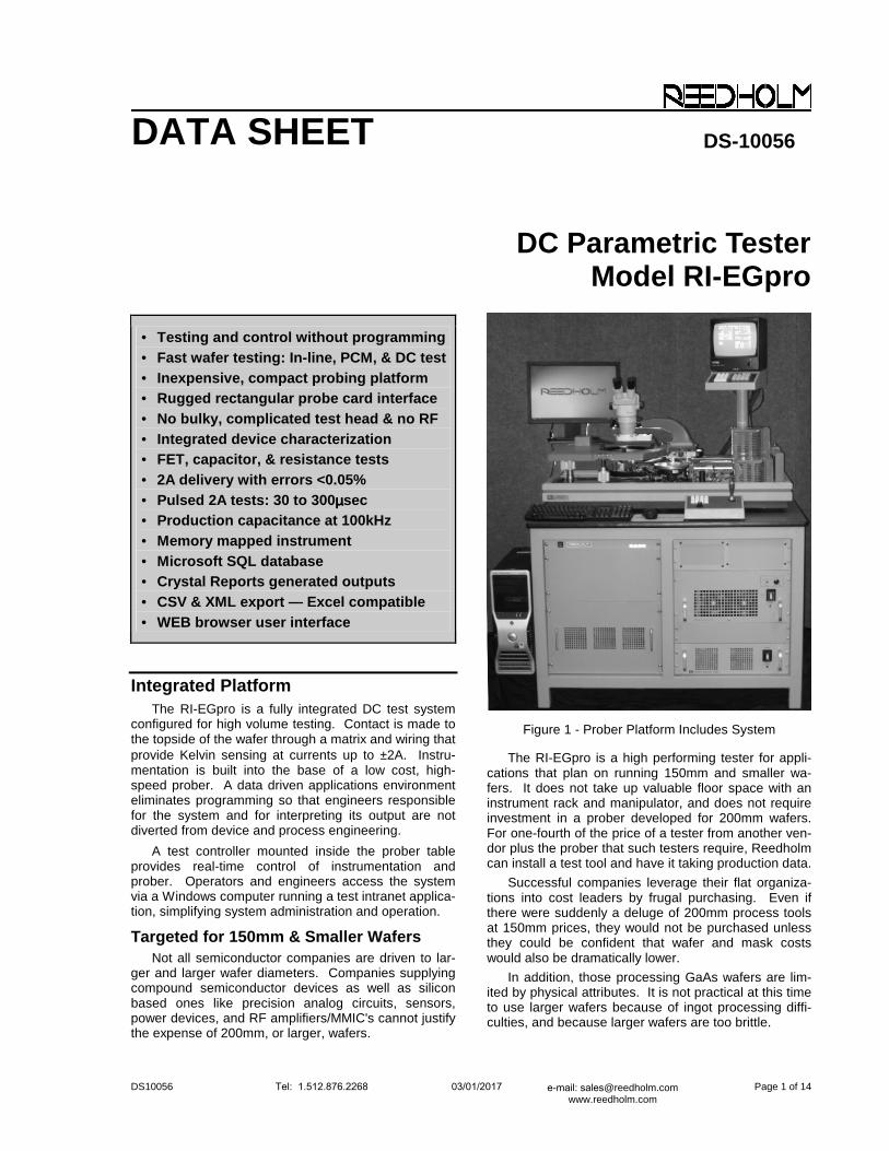
Integrated Platform The RI-EGpro is a fully integrated DC test system
configured for high volume testing. Contact is made to the topside of the wafer through a matrix and wiring that provide Kelvin sensing at currents up to ±2A. Instru-mentation is built into the base of a low cost, high-speed prober. A data driven applications environment eliminates programming so that engineers responsible for the system and for interpreting its output are not diverted from device and process engineering.
A test controller mounted inside the prober table provides real-time control of instrumentation and prober. Operators and engineers access the system via a Windows computer running a test intranet applica-tion, simplifying system administration and operation.
Targeted for 150mm & Smaller Wafers Not all semiconductor companies are driven to lar-
ger and larger wafer diameters. Companies supplying compound semiconductor devices as well as silicon based ones like precision analog circuits, sensors, power devices, and RF amplifiers/MMIC's cannot justify the expense of 200mm, or larger, wafers.
Figure 1 - Prober Platform Includes System
The RI-EGpro is a high performing tester for appli-cations that plan on running 150mm and smaller wa-fers. It does not take up valuable floor space with an instrument rack and manipulator, and does not require investment in a prober developed for 200mm wafers. For one-fourth of the price of a tester from another ven-dor plus the prober that such testers require, Reedholm can install a test tool and have it taking production data.
Successful companies leverage their flat organiza-tions into cost leaders by frugal purchasing. Even if there were suddenly a deluge of 200mm process tools at 150mm prices, they would not be purchased unless they could be confident that wafer and mask costs would also be dramatically lower.
In addition, those processing GaAs wafers are lim-ited by physical attributes. It is not practical at this time to use larger wafers because of ingot processing diffi-culties, and because larger wafers are too brittle.
DATA SHEET DS-10056
DC Parametric TesterModel RI-EGpro
• Testing and control without programming• Fast wafer testing: In-line, PCM, & DC test• Inexpensive, compact probing platform• Rugged rectangular probe card interface• No bulky, complicated test head & no RF• Integrated device characterization• FET, capacitor, & resistance tests• 2A delivery with errors <0.05%• Pulsed 2A tests: 30 to 300 µµµµsec• Production capacitance at 100kHz• Memory mapped instrument• Microsoft SQL database• Crystal Reports generated outputs• CSV & XML export — Excel compatible• WEB browser user interface

DS10056 03/01/2017 Page 2 of 14 Tel: 1.512.876.2268 email: [email protected] www.reedholm.com
No Instrumentation Footprint Clean room space, whether in the fab or on the test
floor, is extremely expensive. Layout dimensions in figure 2 illustrate floor space needs of the RI-EGpro. Some Reedholm customers move the monitor and key-board to the prober table to save even more floor space. Competitive systems require a footprint almost as large as the prober just for the instrumentation.
Figure 2 - Layout with Table for Monitor & Keyboard
Uncontrolled 200mm Tester Costs Companies that process wafers <150mm in diame-
ter are not well served when test system vendors focus on 200mm and larger wafers:
• Since it costs so much for process tools in a200mm or larger fab, selling prices for testers,test head manipulators, and probers have risenwith little constraint.
• Since 200mm and larger fabs are huge com-pared to fabs running smaller wafers, floorspace is not as jealously guarded, and it doesnot matter how many testers it takes for processcontrol. As a result, neither tester/prober foot-print nor testing speed is important. If the testtool is not fast enough, more are purchasedwithout much impact on overall cost or space.
Savings by Eliminating the Test Head Test heads with competitive systems are so heavy
that an expensive prober is needed just to carry the weight. Instead of a low cost prober that Reedholm can supply, one of those systems results in spending two or three times as much for a prober that is probably much slower and more expensive to maintain.
In addition, operators usually cannot handle heavy test heads, so an expensive manipulator is needed.
Lastly, those heavy, bulky test heads require five to ten minutes for probe card change outs. The diagram in figure 3 is roughly to scale for a rack system with test head and manipulator that takes as much floor space as the RI-EGpro. In addition, a prober capable of carry-ing the weight of the test head takes half again as much space as the RI-EG prober.
Figure 3 - Floor Space Savings with RI-EGpro
In-Process, PCM, and DC Test Reedholm systems can be used for the gamut of
DC testing in any semiconductor fab.
In-Line Process Testing Compound semiconductor fabs gather in-process
data such as ohmic contacts, transmission line length, resistivity of active areas, plus gate, mesa, and resistor patterning for process tweaking or gate keeping. Some silicon fabs use a parametric tester for similar purposes.
With Reedholm software, one test list can be used with a myriad of processes. To accomplish that, indi-vidual tests in a list can be designated to execute:
• During and after a particular process step• Regardless of the process step• With process specific pass/fail limits
Thus, data from in-line process testing is identifiable and accessible by lot ID and paired process step.
DS10056 03/01/2017 Page 3 of 14 Tel: 1.512.876.2268 email: [email protected] www.reedholm.com
Process Control Monitoring End-of-line process control measurements of tran-
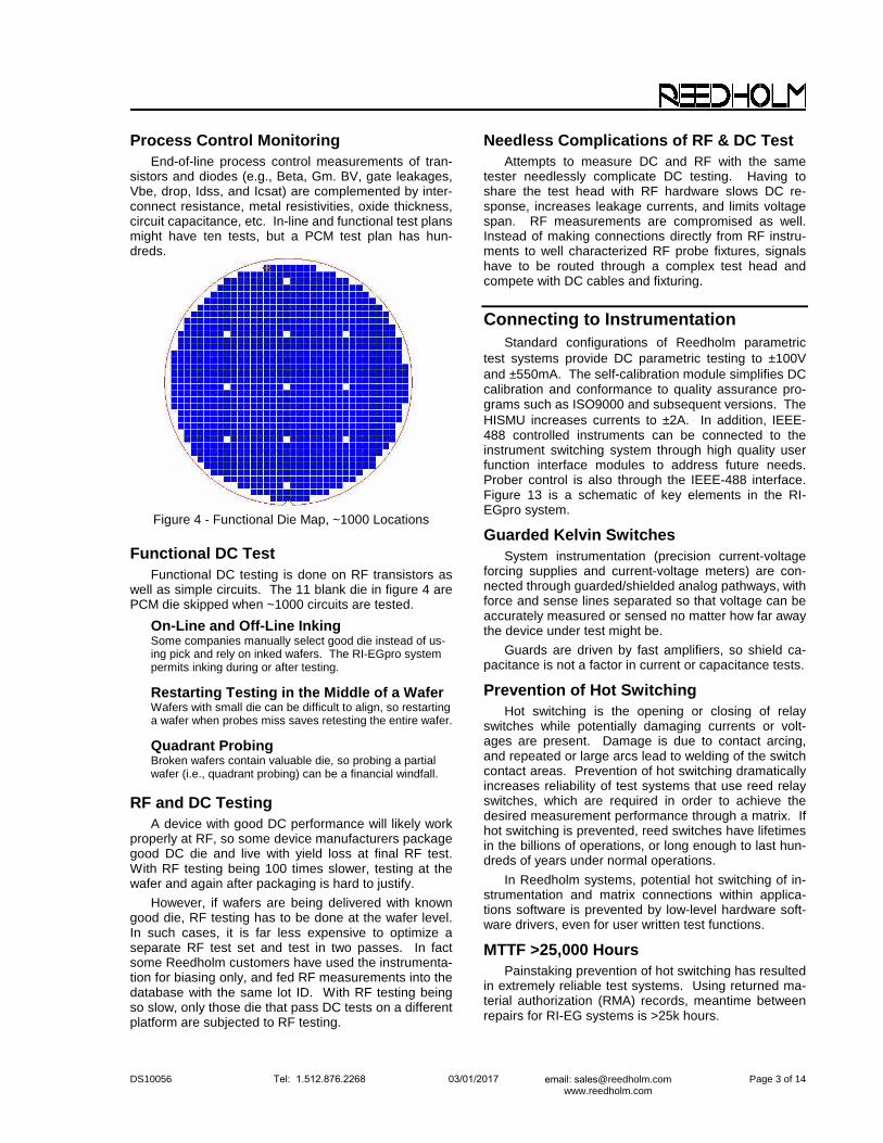
sistors and diodes (e.g., Beta, Gm. BV, gate leakages, Vbe, drop, Idss, and Icsat) are complemented by inter-connect resistance, metal resistivities, oxide thickness, circuit capacitance, etc. In-line and functional test plans might have ten tests, but a PCM test plan has hun-dreds.
Figure 4 - Functional Die Map, ~1000 Locations
Functional DC Test Functional DC testing is done on RF transistors as
well as simple circuits. The 11 blank die in figure 4 are PCM die skipped when ~1000 circuits are tested.
On-Line and Off-Line Inking Some companies manually select good die instead of us-ing pick and rely on inked wafers. The RI-EGpro system permits inking during or after testing.
Restarting Testing in the Middle of a Wafer Wafers with small die can be difficult to align, so restarting a wafer when probes miss saves retesting the entire wafer.
Quadrant Probing Broken wafers contain valuable die, so probing a partial wafer (i.e., quadrant probing) can be a financial windfall.
RF and DC Testing A device with good DC performance will likely work
properly at RF, so some device manufacturers package good DC die and live with yield loss at final RF test. With RF testing being 100 times slower, testing at the wafer and again after packaging is hard to justify.
However, if wafers are being delivered with known good die, RF testing has to be done at the wafer level. In such cases, it is far less expensive to optimize a separate RF test set and test in two passes. In fact some Reedholm customers have used the instrumenta-tion for biasing only, and fed RF measurements into the database with the same lot ID. With RF testing being so slow, only those die that pass DC tests on a different platform are subjected to RF testing.
Needless Complications of RF & DC Test Attempts to measure DC and RF with the same
tester needlessly complicate DC testing. Having to share the test head with RF hardware slows DC re-sponse, increases leakage currents, and limits voltage span. RF measurements are compromised as well. Instead of making connections directly from RF instru-ments to well characterized RF probe fixtures, signals have to be routed through a complex test head and compete with DC cables and fixturing.
Connecting to Instrumentation Standard configurations of Reedholm parametric
test systems provide DC parametric testing to ±100V and ±550mA. The self-calibration module simplifies DC calibration and conformance to quality assurance pro-grams such as ISO9000 and subsequent versions. The HISMU increases currents to ±2A. In addition, IEEE-488 controlled instruments can be connected to the instrument switching system through high quality user function interface modules to address future needs. Prober control is also through the IEEE-488 interface. Figure 13 is a schematic of key elements in the RI-EGpro system.
Guarded Kelvin Switches System instrumentation (precision current-voltage
forcing supplies and current-voltage meters) are con-nected through guarded/shielded analog pathways, with force and sense lines separated so that voltage can be accurately measured or sensed no matter how far away the device under test might be.
Guards are driven by fast amplifiers, so shield ca-pacitance is not a factor in current or capacitance tests.
Prevention of Hot Switching Hot switching is the opening or closing of relay
switches while potentially damaging currents or volt-ages are present. Damage is due to contact arcing, and repeated or large arcs lead to welding of the switch contact areas. Prevention of hot switching dramatically increases reliability of test systems that use reed relay switches, which are required in order to achieve the desired measurement performance through a matrix. If hot switching is prevented, reed switches have lifetimes in the billions of operations, or long enough to last hun-dreds of years under normal operations.
In Reedholm systems, potential hot switching of in-strumentation and matrix connections within applica-tions software is prevented by low-level hardware soft-ware drivers, even for user written test functions.
MTTF >25,000 Hours Painstaking prevention of hot switching has resulted
in extremely reliable test systems. Using returned ma-terial authorization (RMA) records, meantime between repairs for RI-EG systems is >25k hours.

DS10056 03/01/2017 Page 4 of 14 Tel: 1.512.876.2268 email: [email protected] www.reedholm.com
Memory Mapped Instrument Control The RI-EGpro is controlled by a single board com-
puter (SBC) operating under a version of MS-DOS that provides real-time control and does not have latency issues associated with a multi-tasking operating sys-tem. As a result, timing measurements are accurate and repeatable down to microseconds without using an external timer counter that complicates control without addressing latency issues.
Other system architectures have processors and memories buried inside instrumentation boxes. That approach results in slower communications and lack of control of the overall system state.
With memory mapping, complex commands are transmitted at speeds much faster than achieved with IEEE-488 instrumentation buses or other serial proto-cols. For example, a range command is transmitted from a test plan running on the SBC to an instrument in <2µsec. As a result, the RI-EGpro is inherently faster than systems that depend on older UNIX® or Linux computers as well as newer multi-tasking ones.
In addition to providing higher speed and tighter tim-ing control, memory mapping means that the CPU can read and respond to the entire system state in less time than it takes for a reed relay to change state. This flat control architecture is vitally important in coping with noise generated by device breakdown.
By continuously monitoring the memory map, an un-intended change in any register is a flag that destructive breakdown has occurred. Because communications are so fast, all registers, and especially those controlling relays, can be put back to their proper state before damage from hot switching can occur.
The memory map in figure 5 is generated by a soft-ware maintenance utility that enables bit level examina-tion and control of every instrument register using the same routines that provide uncompromised control over state of the system.
Figure 5 - Memory Map of 256, 8-bit Registers
Currents to ±2A The HISMU is a bipolar output voltage source capa-
ble of supplying load currents up to 5A. Its output is programmable between -10V and +10V over voltage ranges 2.5V, 5V, and 10V at full scale. Separate ampli-fiers drive high and low outputs so Kelvin connections assure accurate voltage delivery and measurement. Maximum current is derived from low voltage system supplies so a separate set of supplies is not required.
As shown in figure 6, the HISMU output is con-nected to the DUT via backplane nodes and matrix pins, or via an auxiliary 8-pin cable. The latter is used when backside connections are made to the wafer.
Figure 6 - HISMU Connections
Pulsing duty cycle shown in figure 7 is controlled at the driver level to make sure that pulses up to ±5A are delivered reliably. Pulse width is settable to 30µs, 100µs, 200µs, or 300µs. Because the higher current output pins are not used for this system, current is lim-ited to ±2A, the maximum amount that can be carried by the matrix modules.
Figure 7 - Duty Cycle for HISMU

DS10056 03/01/2017 Page 5 of 14 Tel: 1.512.876.2268 email: [email protected] www.reedholm.com
Production Capacitance Testing While C-V measurements during development are
done at many frequencies, that is not the case once volume testing begins. Unless there is a severe proc-essing problem in the insulator to semiconductor inter-face, circuit capacitors, oxide thickness monitors, varac-tors, etc. have the same capacitance at 100kHz as at 10kHz, 1MHz, 10MHz, or any frequency in between. In fact, capacitance does not measurably increase until well above 100MHz. The Vishay® plot in figure 8 is for silicon dioxide capacitors, but the same frequency inde-pendence is exhibited by compound semiconductor capacitors, varactors, etc.
Figure 8 - Silicon Oxide Capacitance vs. Frequency
Measurements and Self-Inductance Capacitance measurement is analogous to measur-
ing resistance. That is, voltage can be forced and cur-rent measured, or vice-versa, but with a synchronous detector converting the AC signal to capacitance. A band-pass filter around the measurement frequency removes beat frequency components that show up as low frequency capacitance noise.
A block diagram of a force voltage, measure current capacitance converter is shown in figure 9. The input to the meter in this case is a virtual ground by action of an operational amplifier. Thus, the current through the unknown capacitance Cx is solely due to its reactance and the excitation voltage Vx. The voltage developed across precision capacitor C1 is then converted to DC and digitized. Analysis would be similar if an L-C series circuit that resonates at the measurement frequency replaced the amplifier since input impedance would be zero ohms at resonance.
Figure 9 - Voltage to Current Capacitance
Figure 10 illustrates connections of the meter with a few meters of cabling between the capacitance meter and the device under test.
Figure 10 - Cabling Self-Inductance
With total inductance from HI to LO being 2LL, ap-parent capacitance measured by the meter is:
C = CX/(1 – ω22LLCX); where ω = 2πf
Apparent capacitance, therefore, tends to be larger than actual because of wiring inductance. The following table shows errors for 2LL = 4µH. Note that at 1MHz, the apparent value of a 10nF becomes inductive.
Capacitance 100kHz 1MHz
1pF +0.00016% +0.016%
10pF +0.0016% +0.16%
100pF +0.016% +1.60%
1nF +0.16% +18.8%
10nF +1.6% -173%
Table 1 - Effects of Self-Inductance
Historical Ties to 1MHz Historically, a lot of semiconductor capacitance
measurements have been made at 1MHz. Further-more, many process control measurements are still made at 1MHz despite clear benefits of making them at 100kHz in a production setting.
• Unlike a lab setting with closed Faraday shieldsout to the device under test, trying to do thesame in a DC tester compromises DC testing.
• Noise due to fab equipment is more likely tohave components at 1MHz than at 100kHz, so1MHz measurements are often noisy.
• Cabling of a few meters is self-resonant at a fewMHz, so noise amplification at 1MHz is >100times higher than at 100kHz.
• Errors due to self and mutual inductance pro-duces errors at 1MHz that can be completely ig-nored at 100kHz.
DS10056 03/01/2017 Page 6 of 14 Tel: 1.512.876.2268 e-mail: [email protected]
Process Dependent Differences at 100kHz Any differences between 100kHz measurements
and those at 1MHz, or 10kHz, or frequencies in be-tween are almost always due to incorrect data at one or more of the frequencies. The only known reason is when a poor interface between an oxide and a semi-conductor layer interferes with accumulation.
Correlating 100kHz and 1MHz Data That is not to say that correlating with past, bad
measurements is unusual. In 2008, Reedholm installed a system with a 100kHz meter that was off by 16% compared to 1MHz measurements made on a previous obsolete system. Until the customer test engineer dug through the obsolete source code, he did not know that a previous engineer had plugged in a 16% fudge factor to make data agree with thickness calculations.
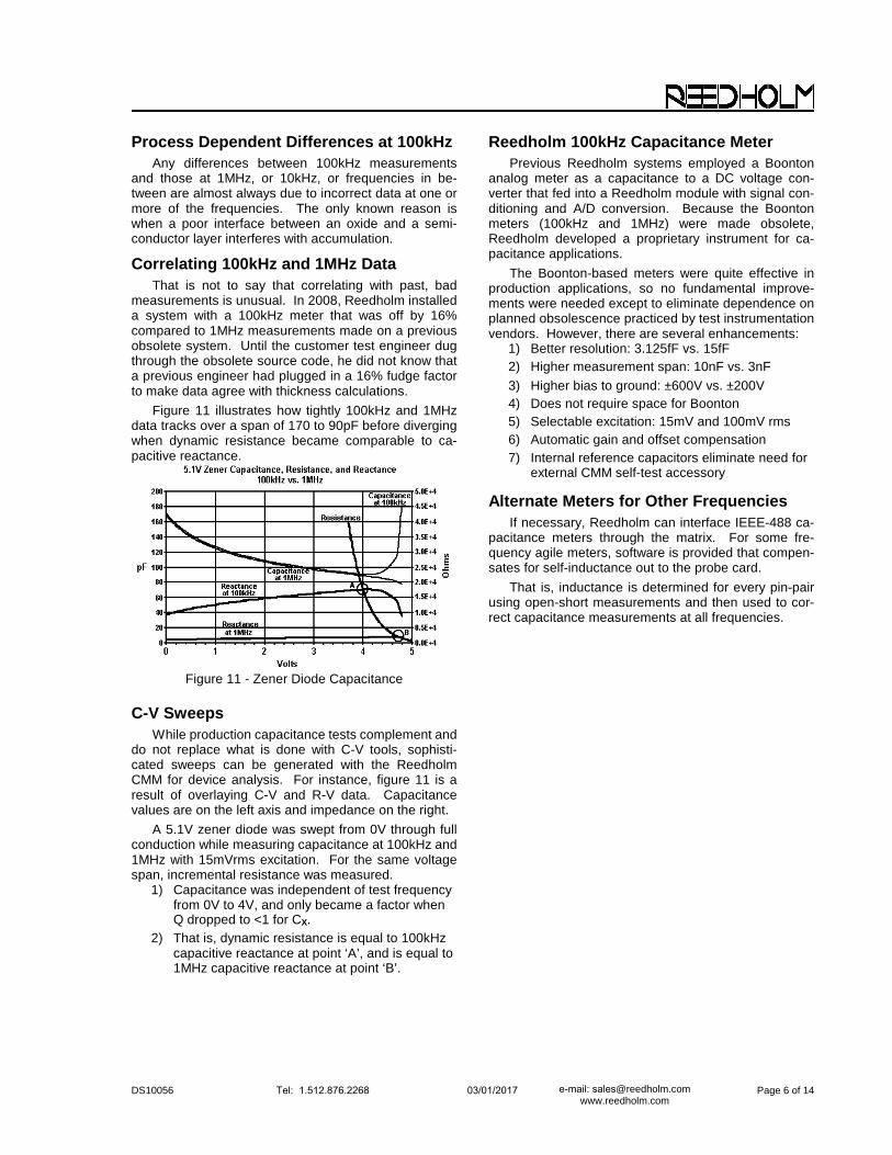
Figure 11 illustrates how tightly 100kHz and 1MHz data tracks over a span of 170 to 90pF before diverging when dynamic resistance became comparable to ca-pacitive reactance.
Figure 11 - Zener Diode Capacitance
C-V SweepsWhile production capacitance tests complement and
do not replace what is done with C-V tools, sophisti-cated sweeps can be generated with the Reedholm CMM for device analysis. For instance, figure 11 is a result of overlaying C-V and R-V data. Capacitance values are on the left axis and impedance on the right.
A 5.1V zener diode was swept from 0V through full conduction while measuring capacitance at 100kHz and 1MHz with 15mVrms excitation. For the same voltage span, incremental resistance was measured.
1) Capacitance was independent of test frequencyfrom 0V to 4V, and only became a factor whenQ dropped to <1 for CX.
2) That is, dynamic resistance is equal to 100kHzcapacitive reactance at point ‘A’, and is equal to1MHz capacitive reactance at point ‘B’.
Reedholm 100kHz Capacitance Meter Previous Reedholm systems employed a Boonton
analog meter as a capacitance to a DC voltage con-verter that fed into a Reedholm module with signal con-ditioning and A/D conversion. Because the Boonton meters (100kHz and 1MHz) were made obsolete, Reedholm developed a proprietary instrument for ca-pacitance applications.
The Boonton-based meters were quite effective in production applications, so no fundamental improve-ments were needed except to eliminate dependence on planned obsolescence practiced by test instrumentation vendors. However, there are several enhancements:
1) Better resolution: 3.125fF vs. 15fF2) Higher measurement span: 10nF vs. 3nF
3) Higher bias to ground: ±600V vs. ±200V4) Does not require space for Boonton5) Selectable excitation: 15mV and 100mV rms6) Automatic gain and offset compensation7) Internal reference capacitors eliminate need for
external CMM self-test accessory
Alternate Meters for Other Frequencies If necessary, Reedholm can interface IEEE-488 ca-
pacitance meters through the matrix. For some fre-quency agile meters, software is provided that compen-sates for self-inductance out to the probe card.
That is, inductance is determined for every pin-pair using open-short measurements and then used to cor-rect capacitance measurements at all frequencies.
DS10056 03/01/2017 Page 7 of 14 Tel: 1.512.876.2268 e-mail: [email protected]
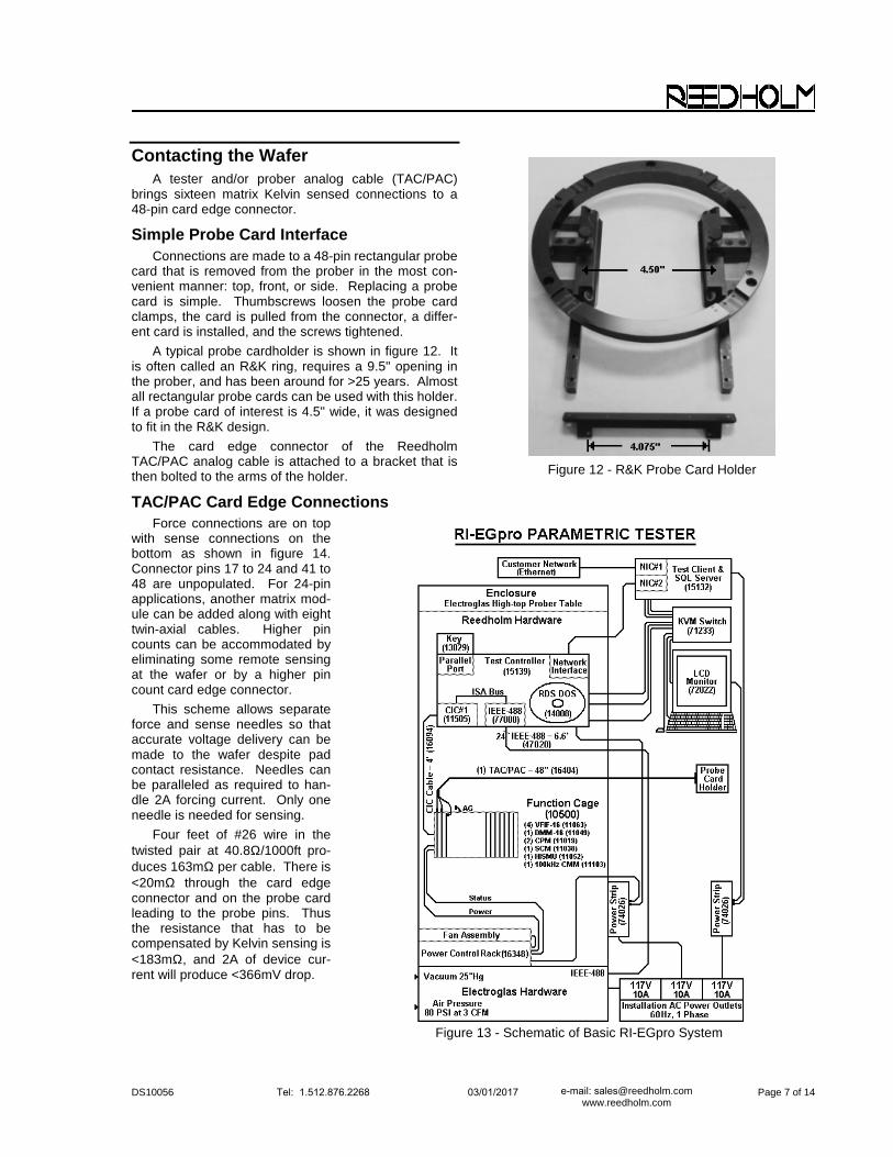
Contacting the Wafer A tester and/or prober analog cable (TAC/PAC)
brings sixteen matrix Kelvin sensed connections to a 48-pin card edge connector.
Simple Probe Card Interface Connections are made to a 48-pin rectangular probe
card that is removed from the prober in the most con-venient manner: top, front, or side. Replacing a probe card is simple. Thumbscrews loosen the probe card clamps, the card is pulled from the connector, a differ-ent card is installed, and the screws tightened.
A typical probe cardholder is shown in figure 12. It is often called an R&K ring, requires a 9.5" opening in the prober, and has been around for >25 years. Almost all rectangular probe cards can be used with this holder. If a probe card of interest is 4.5" wide, it was designed to fit in the R&K design.
The card edge connector of the Reedholm TAC/PAC analog cable is attached to a bracket that is then bolted to the arms of the holder.
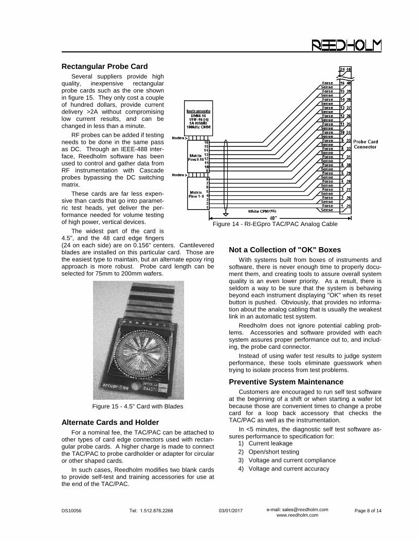
TAC/PAC Card Edge Connections Force connections are on top
with sense connections on the bottom as shown in figure 14. Connector pins 17 to 24 and 41 to 48 are unpopulated. For 24-pin applications, another matrix mod-ule can be added along with eight twin-axial cables. Higher pin counts can be accommodated by eliminating some remote sensing at the wafer or by a higher pin count card edge connector.
This scheme allows separate force and sense needles so that accurate voltage delivery can be made to the wafer despite pad contact resistance. Needles can be paralleled as required to han-dle 2A forcing current. Only one needle is needed for sensing.
Four feet of #26 wire in the twisted pair at 40.8Ω/1000ft pro-duces 163mΩ per cable. There is <20mΩ through the card edge connector and on the probe card leading to the probe pins. Thus the resistance that has to be compensated by Kelvin sensing is <183mΩ, and 2A of device cur-rent will produce <366mV drop.
Figure 12 - R&K Probe Card Holder
Figure 13 - Schematic of Basic RI-EGpro System
DS10056 03/01/2017 Page 8 of 14 Tel: 1.512.876.2268 e-mail: [email protected]
Rectangular Probe Card Several suppliers provide high
quality, inexpensive rectangular probe cards such as the one shown in figure 15. They only cost a couple of hundred dollars, provide current delivery >2A without compromising low current results, and can be changed in less than a minute.
RF probes can be added if testing needs to be done in the same pass as DC. Through an IEEE-488 inter-face, Reedholm software has been used to control and gather data from RF instrumentation with Cascade probes bypassing the DC switching matrix.
These cards are far less expen-sive than cards that go into paramet-ric test heads, yet deliver the per-formance needed for volume testing of high power, vertical devices.
The widest part of the card is 4.5", and the 48 card edge fingers (24 on each side) are on 0.156" centers. Cantilevered blades are installed on this particular card. Those are the easiest type to maintain, but an alternate epoxy ring approach is more robust. Probe card length can be selected for 75mm to 200mm wafers.
Figure 15 - 4.5" Card with Blades
Alternate Cards and Holder For a nominal fee, the TAC/PAC can be attached to
other types of card edge connectors used with rectan-gular probe cards. A higher charge is made to connect the TAC/PAC to probe cardholder or adapter for circular or other shaped cards.
In such cases, Reedholm modifies two blank cards to provide self-test and training accessories for use at the end of the TAC/PAC.
Not a Collection of "OK" Boxes With systems built from boxes of instruments and
software, there is never enough time to properly docu-ment them, and creating tools to assure overall system quality is an even lower priority. As a result, there is seldom a way to be sure that the system is behaving beyond each instrument displaying "OK" when its reset button is pushed. Obviously, that provides no informa-tion about the analog cabling that is usually the weakest link in an automatic test system.
Reedholm does not ignore potential cabling prob-lems. Accessories and software provided with each system assures proper performance out to, and includ-ing, the probe card connector.
Instead of using wafer test results to judge system performance, these tools eliminate guesswork when trying to isolate process from test problems.
Preventive System Maintenance Customers are encouraged to run self test software
at the beginning of a shift or when starting a wafer lot because those are convenient times to change a probe card for a loop back accessory that checks the TAC/PAC as well as the instrumentation.
In <5 minutes, the diagnostic self test software as-sures performance to specification for:
1) Current leakage2) Open/short testing3) Voltage and current compliance4) Voltage and current accuracy
Figure 14 - RI-EGpro TAC/PAC Analog Cable

DS10056 03/01/2017 Page 9 of 14 Tel: 1.512.876.2268 e-mail: [email protected]
Software Test Suite The RI-EGpro software suite removes the
roadblocks that prevent non-programmers and test system engineers from getting test plans devel-oped, reports generated, and data analyzed. This suite fulfills all requirements of gathering develop-ment and production data:
• Test creation for PCM or characterization• Centralized distribution of test plans• Test documentation and version control• Storage and exportation of results• Reports and graphical analysis of results• Control of prober and probing patterns• System integrity assurance & calibration
Test Creation without Spawning Code As shown in figure 17, RDS Intranet allows
tests to be created by simply filling in cells for pins, voltages, currents, delays, etc. However, RDS Intranet does not spew out test code in C or some other language that the test engineer then tweaks and maintains forever.
Data Driven Testing Instead of generating code, RDS Intranet
populates fields in a database record that is downloaded to the test controller and executed in real-time without any delays for interpreting or compiling.
The engineer does not have to learn a programming language, document changes to software, track soft-ware, and myriad other tasks needed for proper soft-ware control.
Setting up and controlling test plans is not unlike creating spreadsheet files to manipulate data. Flexibil-ity is more than adequate, yet no one ever asks what language was used to write the spreadsheet program. All that matters is getting results that make sense and that are easily checked when there are yield problems.
Figure 17 - Input and Edit Test Grid
Figure 16 - Schematic Generator

DS10056 03/01/2017 Page 10 of 14 Tel: 1.512.876.2268 e-mail: [email protected]
Feature Rich, Flexible, and no Compiling No compiling is done, yet very sophisticated soft-
ware representing man-years of development performs complex calculations in an interactive mode.
RDS Intranet software provides capability well be-yond what a test engineer could accomplish starting with source code.
In addition to being used to input a rich set of test parameters, integrated prober control and test stor-age/manipulation features are also data driven.
Not a Limited Set of "Canned" Routines "Canned” source code routines frequently lack the
ability to test many device permutations, and that is why source code has to be customized. However, the RDS Intranet test engine supports:
• Multiple pins per DUT leg (drain, gate, etc.)• Biasing and grounding extra DUT pins• Forcing voltage or current on extra pins• Executing user input equations• Using prior test results for test conditions
After a test is created and found effective, being a record makes it easy to copy and use as the starting point of setting up a new test.
More Than Windows The Intranet user interface is a WEB application, not
just a Windows program. That makes it straightforward to permit database access by all who might need it while still providing security. Thus, a device engineer could answer his or her test questions without having to call a meeting or requesting information from the person with testing responsibility.
No Test Engine Ambiguity Suspect test data can sometimes be traced to im-
proper test conditions or algorithms. With Reedholm software, algorithms are not subject to uncontrolled tweaking, so valuable time is not spent trying to work backwards through code changes.
Since data used to control testing is in a centralized and controlled database, retrieving it eliminates ambigu-ity over what test conditions were used for suspect data. Engineers unfamiliar with Reedholm software, but who have critical knowledge about the issue, can be brought into the discussion by using automatically gen-erated test schematics shown in figure 16.
No Compromise on Test Speed The flat, memory mapped architecture is inherently
faster than possible with multiple instruments, each having processors for control. Test code execution speed is as fast as the most optimized version of com-piled code. Data driven testing is sometimes misinter-preted as having an interpreter level. But that could not be further from the truth. Data is not moved or modified during software execution, so speed is the same as if data were compiled with the code.
Delays and result averaging to reduce noise are the major reasons for slow testing. Those creep into com-piled routines, and programming engineers never seem to have time to take them out. With Reedholm soft-ware, delays and averaging are selected with as much flexibility as needed to match what is found with re-sponse versus time plots that are unique to Reedholm.
After a test plan is set up for volume testing, reports like that in figure 18 can be generated to identify test speed bottlenecks to review for further speed increases. Inclusive of prober movement, test time per site was 600msec for this SIC wafer tested at 2kV.
Figure 18 - Test Time Report from Acquire

DS10056 03/01/2017 Page 11 of 14 Tel: 1.512.876.2268 e-mail: [email protected]
One to Many Linking Using a test in more than one list is simple because
each test is a database record that can be linked and used in any number of test lists. Maintaining test lists across multiple processes and products is simplified when a test only has to be changed once for the new version to be applied every place it is used.
This attribute of linking one to many is extended to test lists, probe patterns, report options, pass-fail set-tings, etc.
Data Storage and Extraction During training, the engineer tasked with bringing
the RI-EGpro tester on-line is shown how to input test data, investigate and optimize results, and control the prober. What he or she does not have to do is figure out what to do with test data. That is, decide:
• Where to store?• What format to use?• How to provide access?
These questions are moot because all data is in anSQL Server database accessed directly or with Reed-holm reporting and analysis tools, one of which is the wafer map shown in figure 19.
Figure 19 - Examine Wafer Map
Exporting Data In addition, data can be automatically exported in
CSV (flat ASCII) and XML file formats compatible with most spreadsheets, databases, and analysis packages.
Many Reedholm customers use Excel® to augment the Crystal Reports package provided with each system and that Reedholm used to generate standard lot and wafer reports.
Integrated Device Characterization The WEB user interface provides full control over
the tester, yet allows it to perform as a curve tracer. It is not necessary to take a wafer to another station to generate characteristic curves like the bipolar transistor curve in figure 20 and the MOSFET curve in figure 21.
Properly used, this capability eliminates uncertainty about device behavior and what test conditions to use to assure the highest quality data. A curve, or set of curves, can be created for almost every test type listed in table 2.
Figure 20 – Bipolar Collector Characteristics
Figure 21 – Depletion MOSFET Drain Characteristics
DS10056 03/01/2017 Page 12 of 14 Tel: 1.512.876.2268 e-mail: [email protected]
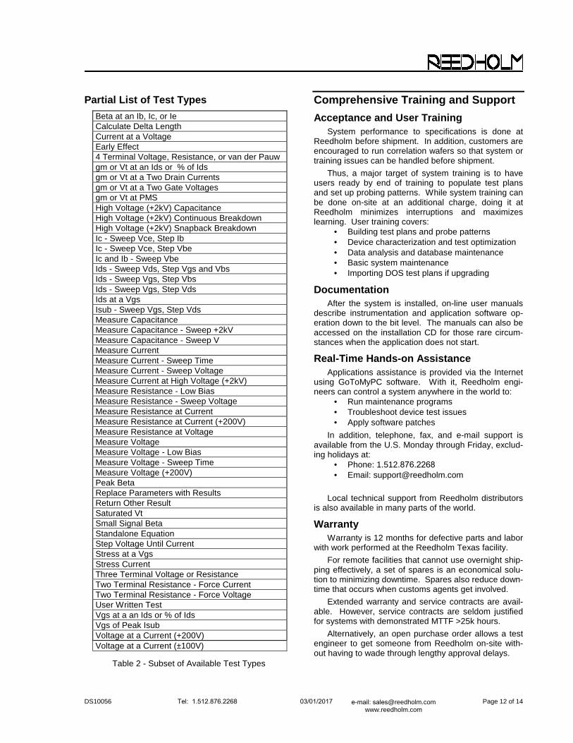
Partial List of Test Types
Beta at an Ib, Ic, or Ie Calculate Delta Length Current at a Voltage Early Effect 4 Terminal Voltage, Resistance, or van der Pauw gm or Vt at an Ids or % of Ids gm or Vt at a Two Drain Currents gm or Vt at a Two Gate Voltages gm or Vt at PMS High Voltage (+2kV) Capacitance High Voltage (+2kV) Continuous Breakdown High Voltage (+2kV) Snapback Breakdown Ic - Sweep Vce, Step Ib Ic - Sweep Vce, Step Vbe Ic and Ib - Sweep Vbe Ids - Sweep Vds, Step Vgs and Vbs Ids - Sweep Vgs, Step Vbs Ids - Sweep Vgs, Step Vds Ids at a Vgs Isub - Sweep Vgs, Step Vds Measure Capacitance Measure Capacitance - Sweep +2kV Measure Capacitance - Sweep V Measure Current Measure Current - Sweep Time Measure Current - Sweep Voltage Measure Current at High Voltage (+2kV) Measure Resistance - Low Bias Measure Resistance - Sweep Voltage Measure Resistance at Current Measure Resistance at Current (+200V) Measure Resistance at Voltage Measure Voltage Measure Voltage - Low Bias Measure Voltage - Sweep Time Measure Voltage (+200V) Peak Beta Replace Parameters with Results Return Other Result Saturated Vt Small Signal Beta Standalone Equation Step Voltage Until Current Stress at a Vgs Stress Current Three Terminal Voltage or Resistance Two Terminal Resistance - Force Current Two Terminal Resistance - Force Voltage User Written Test Vgs at a an Ids or % of Ids Vgs of Peak Isub Voltage at a Current (+200V) Voltage at a Current (±100V)
Table 2 - Subset of Available Test Types
Comprehensive Training and Support
Acceptance and User Training System performance to specifications is done at
Reedholm before shipment. In addition, customers are encouraged to run correlation wafers so that system or training issues can be handled before shipment.
Thus, a major target of system training is to have users ready by end of training to populate test plans and set up probing patterns. While system training can be done on-site at an additional charge, doing it at Reedholm minimizes interruptions and maximizes learning. User training covers:
• Building test plans and probe patterns• Device characterization and test optimization• Data analysis and database maintenance• Basic system maintenance• Importing DOS test plans if upgrading
Documentation After the system is installed, on-line user manuals
describe instrumentation and application software op-eration down to the bit level. The manuals can also be accessed on the installation CD for those rare circum-stances when the application does not start.
Real-Time Hands-on Assistance Applications assistance is provided via the Internet
using GoToMyPC software. With it, Reedholm engi-neers can control a system anywhere in the world to:
• Run maintenance programs• Troubleshoot device test issues• Apply software patches
In addition, telephone, fax, and e-mail support is available from the U.S. Monday through Friday, exclud-ing holidays at:
• Phone: 1.512.876.2268• Email: [email protected]
Local technical support from Reedholm distributors is also available in many parts of the world.
Warranty Warranty is 12 months for defective parts and labor
with work performed at the Reedholm Texas facility.
For remote facilities that cannot use overnight ship-ping effectively, a set of spares is an economical solu-tion to minimizing downtime. Spares also reduce down-time that occurs when customs agents get involved.
Extended warranty and service contracts are avail-able. However, service contracts are seldom justified for systems with demonstrated MTTF >25k hours.
Alternatively, an open purchase order allows a test engineer to get someone from Reedholm on-site with-out having to wade through lengthy approval delays.
DS10056 03/01/2017 Page 13 of 14 Tel: 1.512.876.2268 e-mail: [email protected]
Specifications Instrument specifications apply at the end of the
TAC/PAC analog cable without a probe card attached. Some commonly used wafer test accessories (espe-cially probe cards) reduce parametric testing accuracy at low currents. Care is needed in designing the test environment to achieve maximum performance.
Use Conditions Temperature: 18°–28°C
Humidity: 30%–50% R.H. Non-Condensing
Nominal Power: 117V, 50 or 60Hz Regulated supplies isolate instrumentation from
power line variations of more than ±10%. Voltages different than nominal are addressed with step up or step down transformers.
Basic Switching System Specifications for low noise, high performance ma-
trix switching apply to user function interface modules as well as the CPM and node switches of instruments.
1) Maximum Stand-off Voltage: ±600V2) Maximum Carrying Current: ±2A3) Leakage Resistance: 1 x 10¹²Ω/System Pin Count4) Pin-to-Pin Thermal EMF: <±100µV Max5) Pin-to-Pin Resistance (shorted): <400mΩ6) Switching Speed (including software delay): 1ms
Automated DC Calibration Unlike instrument boxes with internal self-
calibration, a separate Self Calibration Module (SCM) provides independent confirmation that instrument modules are calibrated. It should be run once per quar-ter.
The SCM has an accurate, stable voltage reference coupled with an instrument grade high voltage amplifier provides precision currents and voltages for all of the DC instruments. In operation, the SCM is used to gen-erate offset and gain error correction factors for DC instruments, after which the factors are used to prevent source errors and to compensate for measurement er-rors. As long as the self-calibration software can cor-rect module accuracy, the module meets its accuracy specifications.
SCM Transfer Accuracy (24 Hr, ±2C°)Voltage
Range (V) Error
(% of Value) Current
Range (A) Error
(% of Value) 0.25 0.05 100n 0.04 0.50 0.03 1µ 0.02 1.00 0.02 10µ 0.02 2.50 0.01 100µ 0.02 5.00 0.01 1m 0.02 10.0 0.01 10m 0.02 25.0 0.01 100m N/A 50.0 0.01 1 N/A 100 0.01
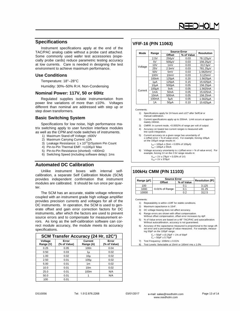
VFIF-16 (P/N 11063)
Source Error Mode Range Offset % of Value
Resolution
2.5V 250µV 0.03 78.125µV 5V 500µV 0.03 156.25µV 10V 1mV 0.03 312.5µV 25V 2.5mV 0.03 781.25µV 50V 5mV 0.03 1.5625mV
Voltage
100V 10mV 0.03 3.125mV 100nA 125pA 0.20 1.5625pA 1µA 125pA 0.15 15.625pA 10µA 500pA 0.05 156.25pA 100µA 5nA 0.05 1.5625nA 1mA 50nA 0.05 15.625nA 10mA 500nA 0.05 156.25nA 100mA 5µA 0.05 1.5625µA
Current
1A 50µA 0.10 15.625µA
Comments:
1) Specifications apply for 24 hours and ±1Cº after SelfCal ormanual calibration.
2) Current specifications apply up to 200mA. Limit occurs at approxi-mately 240mA.
3) CMRR: In current mode, <0.0002% of range per volt of output
4) Accuracy on lowest two current ranges is measured withline cycle integration.
5) Current accuracy on a given range has uncertainty of ± (offset error + % of value error). For example, forcing 100µA on the 100µA range results in:
Iout = 100µA ± (5nA + 0.05% of 100µA) Iout = 100µA ± 55nA
6) Voltage accuracy uncertainty is ± (offset error + % of value error). Forexample, forcing 1V on the 2.5V range results in:
Vout = 1V ± (78µV + 0.03% of 1V) Vout = 1V ± 378µV
100kHz CMM (P/N 11103)
Sourc e Error Range (pF) Offset % of Value
Resolution (fF)
100 0.1 3.125 1000 0.1 31.25 10000
0.01% of Range 0.2 312.5
Comments:
1) Repeatability is within ±10fF for stable conditions.
2) Maximum capacitance is 10nF.
3) DC voltage biasing does not affect accuracy.
4) Range errors are shown with offset compensation. Without offset compensation, offset error increases by 4pF.
5) % of Value errors are based on a 48" TAC/PAC and autocalibration.Without autocalibration, accuracy is not guaranteed.
6) Accuracy of the capacitance measured is proportional to the range off-set error and a percentage of value measured. For example, measur-ing 50pF on the 100pF range:
Cx = 50pF ± (0.25pF + 1% of 50pF Cx = 50pF ± 0.75pF
7) Test Frequency: 100kHz ± 0.01%
8) Test Levels: Selectable at 15mV or 100mV rms ± 1.0%

DS10056 03/01/2017 Page 14 of 14 Tel: 1.512.876.2268 email; [email protected] www.reedholm.com
Digital Multimeter (P/N 11049)
Source Error Mode Range Offset % of Value
Resolution
250mV 250µV (50µV) 0.03 7.8125µV 500mV 250µV (50µV) 0.03 15.625µV
1V 300µV (75µV) 0.03 31.25µV 2.5V 500µV (100µV) 0.03 78.125µV 5V 1mV (200µV) 0.03 156.25µV 10V 2mV (400µV) 0.03 312.5µV 25V 5mV (1mV) 0.03 781.25µV 50V 10mV (2mV) 0.03 1.5625mV
Voltage
100V 20mV (4mV) 0.03 3.125mV 100nA 100pA 0.20 3.125pA 1µA 300pA 0.15 31.25pA 10µA 2nA 0.05 312.5pA 100µA 20nA 0.05 3.125nA 1mA 200nA 0.05 31.25nA 10mA 2µA 0.05 312.5nA 100mA 20µA 0.05 3.125µA
Current
1A 200µA 0.10 31.25µA
Comments:
1) Specifications apply for 24 hours and ±1Cº after SelfCal ormanual calibration.
2) Maximum output current on 1A range is ±350mA.On other ranges, maximum is 125% of range.
3) Settling time to 0.01%:
4.0ms, 100nA Range 2.3ms, 1µA Range 1.7ms, 10µA-1A Ranges 1.6ms, 250mV-100V Ranges
4) CMRR Voltage:
5µV/V (106dB)
5) CMRR Current::
1 ppm of range per volt, 10µA -1A 2 ppm of range per volt, 1µA 6 ppm of range per volt, 100nA
6) Accuracy of the lowest three current ranges is determined with digitalaveraging approximating line cycle integration.
7) Accuracy of current measured on a given range is proportional to range and a percentage of current being measured. For example,measuring 50µA on the 100µA range would have uncertainty of:
50µA ± (20nA + 0.05% of 50µA) = 50µA ± 45nA
8) Range offset errors shown in parentheses () apply for an eight-hourperiod after auto zero and for ±1C°.
9) When measuring currents from sources with non-zero output conduc-tance, the following is added to the error specifications:
±(830 ppm of value +151µA)/mho
HISMU (P/N 11052)
Source Error Mode Range Offset % of Value
Resolution
Current 10A 2.5mA 0.10 2.5mA 2.5V 2.5mV 0.05 1.25mV 5V 5mV 0.05 2.5mV Voltage 10V 10mV 0.05 5mV
Comments:
1) Analog settling time is <5µs to within 0.1%.
2) Pulse width uncertainty is <1µs.
3) Accuracy of voltage forced on a given range is a function of the range offset error and the value forced, for example, forcing 1.25V on the 2.5V range results in:
Vout = 1.25V ± (2.5mV + 0.05% of 1.25V) Vout = 1.25V ± 3.125mV
4) Accuracy of current measured is a function of the range offset errorand the value measured, for example, measuring 1A on the 10A range results in:
Iout = 1A ± (2.5mA + 0.1% of 1A) Iout = 1A ± 3.5mA
Acquire, Build, ChargeScope, EMAGE, EMPAC, EMREL, Examine, GrafPAC, RDS DOS, and RDS Intranet are trademarks of Reedholm Systems. All other company and/or product names are trademarks of their respective companies. Copyright © 2017 Reedholm Systems Co.