data sheet - mxchipen.mxchip.com/download/getfiles/57391c8444837.pdf/datasheet.pdf · data sheet...
TRANSCRIPT

1
Overview
EMW3162 is a low-power embedded Wi-Fi module integrates a wireless LAN MAC/baseband /radio,
and a Cortex-M3 microcontroller STM32F205 that runs a unique "self-hosted" Wi-Fi networking
library and software application stack. EMW3162 has 1M bytes flash, 128k RAM and rich peripherals
for your embedded Wi-Fi applications.
EMW3162 is also an mxchipWNetTM compatible platform; users can build their own embedded Wi-Fi
applications based on mxchipWNetTM library which manage all of the Wi-Fi MAC and TCP/IP stack
processing. We also provide several mxchipWNetTM firmwares to meet typical applications: wireless
UART, wireless audio, wireless sensor etc.
When using mxchipWNetTM -DTU firmware, you can establish Wi-Fi networking for any device with a
micro-controller and a UART interface. Quick development cycles enable fast time to market.
EMW3162 and EMW3280 are pin compatible.
Applications
Building Automation / Access
Control
Smart home appliances
Medical/Health Care
Industrial Automation Systems
Point Of Sale system (POS)
Auto electronics
Product list
Module Antenna Note
EMW3162-P On-board PCB antenna Default
EMW3162-E IPEX connector optional
Firmware/Library
Firmware/Library Function
mxchipWNetTM
-DTU
Prede fined firmware
UART/Wi-Fi conversion
mxchipWNetTM
Library
Software library used to
develop custom firmware
mxchipWNetTM
Library Plus Software library based on RTOS
WICEDTM
Firmware
development kit
WICEDTM source codes with
TCP/IP, Wi-Fi MAC RTOS and
GCC tool chain
Data Sheet
EMW3162
Embedded Wi-Fi module
V2.5 Date:2016-03-14 NO:DS0006E

2
Contents
1 INTRODUCTION ................................................................................................................................................... 5
Product is introduced ........................................................................................................................................... 5 1.1
Product appearance .............................................................................................................................................. 5 1.2
Hardware block diagram ..................................................................................................................................... 5 1.3
Features ..................................................................................................................................................................... 6 1.4
LED ............................................................................................................................................................................... 7 1.5
2 PINS .......................................................................................................................................................................... 8
Pin Designation ....................................................................................................................................................... 8 2.1
Recommended packages .................................................................................................................................... 8 2.2
Pin Arrangement .................................................................................................................................................... 9 2.3
3 ELECTRICAL PARAMETERS ............................................................................................................................. 12
Absolute maximum ratings: .............................................................................................................................. 12 3.1
3.1.1 Voltage & Current ................................................................................................................................ 12
Operating conditions .......................................................................................................................................... 12 3.2
3.2.1 WLAN Subsystem ................................................................................................................................. 13
3.2.2 Microcontroller Subsystem ............................................................................................................... 14
Digital I/O port characteristics......................................................................................................................... 16 3.3
3.3.1 Output voltage levels .......................................................................................................................... 16
3.3.2 Output voltage levels .......................................................................................................................... 16
3.3.3 nRESET pin characteristics ................................................................................................................. 17
Other MCU electrical parameters ................................................................................................................... 17 3.4
Temperature and Humidity ............................................................................................................................... 17 3.5
ESD ............................................................................................................................................................................ 18 3.6
Static latch-up ........................................................................................................................................................ 18 3.7
RF characteristics .................................................................................................................................................. 18 3.8
3.8.1 Basic RF characteristics ....................................................................................................................... 18
3.8.2 IEEE802.11b mode ............................................................................................................................... 19
3.8.3 IEEE802.11g mode ............................................................................................................................... 19
3.8.4 IEEE802.11n 20MHz bandwidth mode .......................................................................................... 21
4 ANTENNA INFORMATION ............................................................................................................................. 23
Minimizing radio interference ......................................................................................................................... 23 4.1
U.F.L RF Connector ............................................................................................................................................... 24 4.2
5 MECHANICAL DIMENSIONS ......................................................................................................................... 25
EMW3162 Mechanical Dimensions ................................................................................................................ 25 5.1
Use guidelines (Please read carefully) ........................................................................................................... 26 5.2
The matters needing attention ........................................................................................................................ 28 5.3

3
MSL/Storage Condition ...................................................................................................................................... 29 5.4
Recommended Reflow Profile .......................................................................................................................... 30 5.5
6 REFERENCE CIRCUIT ........................................................................................................................................ 31
7 5 V UART UART - 3.3V UART CONVERSION REFERENCE CIRCUIT .................................................. 33
8 SALES INFORMATION AND TECHNICAL SUPPORT .............................................................................. 34
9 VERSION UPDATE INSTRUCTIONS ............................................................................................................. 35
List of Tables
Table 1. LED functions ................................................................................................................................................. 7
Table 2. EMW3162 pin arrangement ..................................................................................................................... 9
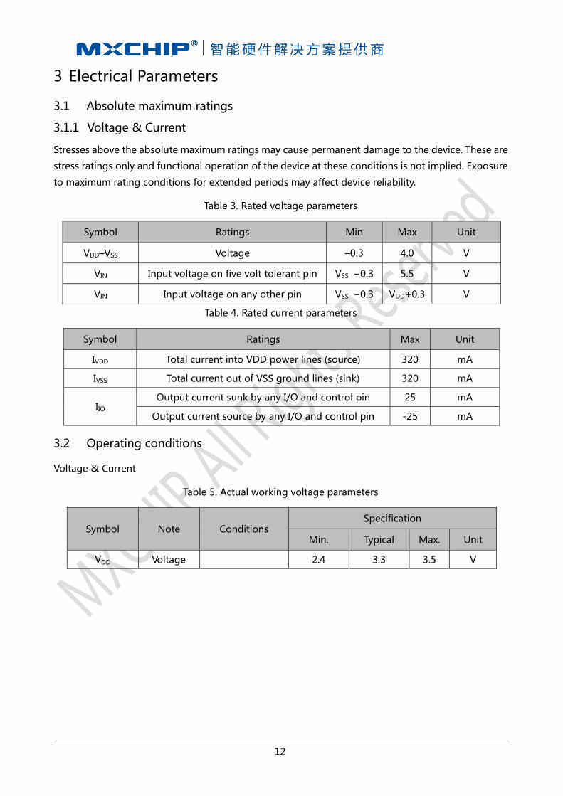
Table 3. Rated voltage parameters ....................................................................................................................... 12
Table 4. Rated current parameters........................................................................................................................ 12
Table 5. Actual working voltage parameters ..................................................................................................... 12
Table 6. Actual working current parameters ..................................................................................................... 13
Table 7. "Run Mode" general maximum current power consumption .................................................... 14
Table 8. "Stop Mode" general maximum current power consumption ................................................... 15
Table 9. "Stop Mode" general maximum current power consumption ................................................... 15
Table 10. "Ordinary operation mode" power consumption ........................................................................ 16
Table 11. I/O port output voltage ......................................................................................................................... 16
Table 12. I/O port input voltage ............................................................................................................................ 16
Table 13. nRESET Pin parameters .......................................................................................................................... 17
Table 14. Temperature and Humidity .................................................................................................................. 17
Table 15. ESD parameters ........................................................................................................................................ 18
Table 16. Static latch - up parameters ................................................................................................................. 18
Table 17. RF basic attributes ................................................................................................................................... 18
Table 18. EEE802.11bRF Basic attributes............................................................................................................. 19
Table 19. IEEE802.11b RF Send properties ......................................................................................................... 19
Table 20. IEEE802.11b RF Receive properties .................................................................................................... 19
Table 21. IEEE802.11g RF Basic attributes .......................................................................................................... 19
Table 22. IEEE802.11g RF Send properties ......................................................................................................... 20

4
Table 23. IEEE802.11g RF Receive properties .................................................................................................... 20
Table 24. IEEE802.11n RF Basic attributes .......................................................................................................... 21
Table 25. IEEE802.11n RF Send properties ......................................................................................................... 21
Table 26. IEEE802.11n RF Receive properties .................................................................................................... 22
List of Figures
Figure 1. EMW3162-P ................................................................................................................................................. 5
Figure 2. EMW3162-E .................................................................................................................................................. 5
Figure 3. EMW3162 Hardware block diagram .................................................................................................... 6
Figure 4. LED ................................................................................................................................................................... 7
Figure 5. EMW3162: appearance and pinout ..................................................................................................... 8
Figure 6. EMW3162 Recommend DIP package diagram ................................................................................ 8
Figure 7. EMW3162 Recommend LGA package diagram ............................................................................... 9
Figure 8. ......................................................................................................................................................................... 23
Figure 9. Temperature and humidity indicator CARDS ................................................................................. 27
Figure 10. Storage Condition.................................................................................................................................. 29
Figure 11 . Temperature Curve............................................................................................................................... 30
Figure 12. Power reference circuit ........................................................................................................................ 31
Figure 13 . USB to serial reference circuit .......................................................................................................... 31
Figure 14. Module refer to the external interface circuit .............................................................................. 32
Figure 15. UART UART 5 V - 3.3 V conversion circuit.................................................................................. 33

5
1 Introduction
Product is introduced 1.1
EMW3162 is a low-power embedded Wi-Fi module integrates a wireless LAN MAC/baseband /radio,
and a Cortex-M3 microcontroller STM32F205 that runs a unique "self-hosted" Wi-Fi networking
library and software application stack. EMW3162 has 1M bytes flash, 128k RAM and rich peripherals
for your embedded Wi-Fi applications.
EMW3162 is also an mxchipWNetTM compatible platform; users can build their own embedded Wi-Fi
applications based on mxchipWNetTM library which manage all of the Wi-Fi MAC and TCP/IP stack
processing. We also provide several mxchipWNetTM firmwares to meet typical applications: wireless
UART, wireless audio, wireless sensor etc.
When using mxchipWNetTM-DTU firmware, you can establish Wi-Fi networking for any device with a
micro-controller and a serial interface. Quick development cycles enable fast time to market.
EMW3162 and EMW3280 are pin compatible.
Product appearance 1.2
Figure 1. EMW3162-P
Figure 2. EMW3162-E
Hardware block diagram 1.3
As shown in figure 3, module consists of three parts:
(1) Cortex-M3 MCU
(2) Wi-Fi RF IC
(3) Power management

6
Figure 3. EMW3162 Hardware block diagram
Features 1.4
Single operation voltage:3.3V
Power consumption:
Only ~7mA while module is connected to access point and no data is transmitting,
Only ~24mA while sending data under 20kbps,
Only 8μA under standby mode.
STM32F2 MCU frequency: 120MHz,flash size: 1M bytes,RAM size: 128k bytes.
On-chip functionality Single-chip: MAC/BB/RF
Peripherals:
32 x GPIOs
2 x UARTs,includes hardware flow control
1 x SPI/I2S
8 x ADC input channels,2 DAC output channel
1 x USB OTG, 2 x CAN
1 x I2C
PWM/Timer input/output available on every GPIO pin
SWD debug interface
Wi-Fi connectivity
802.11b, 802.11g, 802.11n (single stream) on channel [email protected]

7
WEP, WPA/WPA2 PSK/Enterprise
Transmit power:18.5dBm@11b,15.5dBm@11g,14.5dBm@11n
MIN Receiver Sensitivity: -96 dBm
Max Data rate:11Mbps@11b,54Mbps@11g,72Mbps@11n HT20
Wi-Fi modes:Station, Soft AP and Wi-Fi direct
Advanced 1x1 802.11n features
Full/Half Guard Interval
Frame Aggregation
Space Time Block Coding (STBC)
Low Density Parity Check (LDPC) Encoding
Hardware Encryption: WEP, WPA/WPA2
WPS 2.0, EasyLink
Multiple power save modes
On-board chip antenna,IPEX connector for external antenna
CE,FCC compliant
Operating Temperature: -40 to 85
MSL level 3
LED 1.5
Figure 4. LED
Name Color GPIO
D1 Green PB0
D2 Red PB1
Table 1. LED functions

8
2 Pins
Pin Designation 2.1
EMW3162 has two kinds of packaging form: The first kind of DIP Package and has two groups of pins
(1x15+1x15x2mm),the lead pitch is 2mm. The second kind of packaging for LAG and has 44 pins(As
shown in Figure 5-red marking),PIN39-PIN44 connect to GND, Suggested that as far as possible
welding.
Pinout is shown in the Figure 5, Red logo PIN are welding plate of the BOTTOM layer.
Figure 5. EMW3162: appearance and pinout
Recommended packages 2.2
Solder window and the same size of the pad. SMT Recommended steel thickness is 0.12mm-0.14mm.
(Unit:mm)
Figure 6. EMW3162 Recommend DIP package diagram

9
Figure 7. EMW3162 Recommend LGA package diagram
Pin Arrangement 2.3
Table 2. EMW3162 pin arrangement
Pins Name Type IO level Main function
(after reset) Alternate functions Other functions
1 PB6 I/O FT PB6 I2C1_SCL/ USART1_TX /
TIM4_CH1 / CAN2_TX
2 PB7 I/O FT PB7 I2C1_SDA / USART1_RX/
TIM4_CH2
3 PA13 I/O FT SWDIO
4 PC7 I/O FT PC7 I2S3_MCK / TIM8_CH2/
TIM3_CH2 / USART6_RX
5 PA3 I/O FT PA3 TIM5_CH4 / TIM9_CH2 /
TIM2_CH4 / ADC123_IN3
6 PA4 I/O TT PA4 SPI1_NSS / SPI3_NSS /
I2S3_WS
ADC12_IN4 /
DAC1_OUT
7 PB3 I/O FT JTDO/
TRACESWO
JTDO/TRACESWO/ I2S3_SCK
/ TIM2_CH2 / SPI1_SCK /
SPI3_SCK/
8 PB4 I/O FT NJTRST NJTRST/ SPI3_MISO /
TIM3_CH1 / SPI1_MISO/

10
Pins Name Type IO level Main function
(after reset) Alternate functions Other functions
9 PB5 I/O FT PB5
I2C1_SMBA / TIM3_CH2 /
SPI1_MOSI/ SPI3_MOSI /
CAN2_RX
10 PB8 I/O FT PB8 TIM4_CH3 / TIM10_CH1 /
I2C1_SCL / CAN1_RX
11 PA1 I/O FT PA1 TIM5_CH2 / TIM2_CH2 ADC123_IN1
12 PC2 I/O FT PC2 ADC123_ IN12
13 PB14 I/O FT PB14 TIM1_CH2N / TIM12_CH1 /
TIM8_CH2N/
14 PC6 I/O FT PC6 TIM8_CH1 / TIM3_CH1 /
USART6_TX
15 GND
16 PB1 I/O PB1 TIM3_CH4 / TIM8_CH3N/
TIM1_CH3N/ ADC12_IN9
17 nRESET
18 PA15 I/O FT JTDI JTDI/ SPI3_NSS/ I2S3_WS/
TIM2_CH1_ETR / SPI1_NSS
19 PB11 I/O FT PB11 TIM2_CH4
20 PA12 I/O FT PA12 USART1_RTS / CAN1_TX/
TIM1_ETR/ OTG_FS_DP
21 PA11 I/O FT PA11 USART1_CTS/CAN1_RX/
TIM1_CH4 / OTG_FS_DM
22 PA9 I/O FT PA9 USART1_TX/ TIM1_CH2 OTG_FS_VBUS
23 PA10 I/O FT PA10 USART1_RX/ TIM1_CH3/
OTG_FS_ID
24 VCC
25 GND
26 NC
27 BOOT0 I BOOT0
28 PA14 I/O JTCK- SWCLK JTCK-SWCLK

11
Pins Name Type IO level Main function
(after reset) Alternate functions Other functions
29 PA0-
WKUP I/O PA0-WKUP
TIM2_CH1_ETR/
TIM5_CH1 / TIM8_ETR
ADC123_IN0/
WKUP
30 PB9 I/O PB9 TIM4_CH4/ TIM11_CH1 /
I2C1_SDA / CAN1_TX
31 PA5 I/O TT PA5 SPI1_SCK / TIM2_CH1_ETR/
TIM8_CHIN
ADC12_IN5
/DAC2_OUT
32 PA6 I/O FT PA6
SPI1_MISO /
TIM8_BKIN/TIM13_CH1 /
TIM3_CH1 / TIM1_BKIN
ADC12_IN6
33 PA7 I/O FT PA7
SPI1_MOSI/ TIM8_CH1N /
TIM14_CH1 TIM3_CH2/ /
TIM1_CH1N
ADC12_IN7
34 PB15 I/O FT PB15 TIM1_CH3N / TIM8_CH3N /
TIM12_CH2 /RTC_50Hz
35 PC3 I/O FT PC3 ADC123_ IN13
36 PC4 I/O FT PC4 ADC12_IN14
37 NC
38 NC
39 GND
40 GND
41 GND
42 GND
43 GND
44
1. FT = 5 V tolerant; TT = 3.6 V tolerant.
2. FT = 5 V tolerant except when in analog mode or oscillator mode (for PC14, PC15, PH0 and
PH1).
3. I = input, O = output, S = supply.
4. STM32 peripherals are not listed if they cannot be presented on current pins.
12
3 Electrical Parameters
Absolute maximum ratings 3.1
3.1.1 Voltage & Current
Stresses above the absolute maximum ratings may cause permanent damage to the device. These are
stress ratings only and functional operation of the device at these conditions is not implied. Exposure
to maximum rating conditions for extended periods may affect device reliability.
Table 3. Rated voltage parameters
Symbol Ratings Min Max Unit
VDD–VSS Voltage –0.3 4.0 V
VIN Input voltage on five volt tolerant pin VSS −0.3 5.5 V
VIN Input voltage on any other pin VSS −0.3 VDD+0.3 V
Table 4. Rated current parameters
Symbol Ratings Max Unit
IVDD Total current into VDD power lines (source) 320 mA
IVSS Total current out of VSS ground lines (sink) 320 mA
IIO Output current sunk by any I/O and control pin 25 mA
Output current source by any I/O and control pin -25 mA
Operating conditions 3.2
Voltage & Current
Table 5. Actual working voltage parameters
Symbol Note Conditions Specification
Min. Typical Max. Unit
VDD Voltage 2.4 3.3 3.5 V

13
3.2.1 WLAN Subsystem
Table 6. Actual working current parameters
Symbol Note Conditions Typical Unit
IRF OFF1 2 μA
IRF SLEEP4 200 μA
IRF Rx(Listen)2 52 mA
IRF Rx(Active)3 59 mA
IRF Power Save5 6 1.9 mA
IRF Tx CCK7 10 11 Mbps at 18.5 dBm 320 mA
IRF Tx OFDM8 10 54 Mbps at 15.5 dBm 270 mA
IRF Tx OFDM9 10 65 Mbps at 14.5 dBm 260 mA
Note 1: Power is off.
Note 2: Carrier Sense (CCA) when no carrier present
Note 3: Carrier Sense (CS) detect/Packet Rx
Note 4: Intra-beacon Sleep
Note 5: Beacon Interval = 102.4ms, DTIM = 1, Beacon duration = 1 ms @1 Mbps.
Integrated Sleep + wakeup + Beacon Rx current over 1 DTIM interval.
Note 6: In WLAN power-saving mode, the following blocks are powered down: Crystal oscillator,
Baseband PLL, AFE, RF PLL, Radio
Note 7: CCK power at chip port. Duty cycle is 100%. Includes PA contribution.
Note 8: OFDM power at chip port. Duty cycle is 100%. Includes PA contribution.
Note 9: OFDM power at chip port is 16 dBm, duty cycle is 100%, includes PA contribution.
Note 10: Absolute junction temperature limits maintained through active thermal monitoring and
dynamic Tx duty cycle limiting.

14
3.2.2 Microcontroller Subsystem
Typical and maximum current consumption in Run mode, code with data processing running from
Flash memory (ART accelerator enabled) or RAM
Table 7. "Run Mode" general maximum current power consumption
Symbol Conditions fHCLK Running Mode Sleep Mode
Unit TA=25°C TA=25°C
IMCU
External clock, all
peripherals enabled
120MHz 49 38
mA
90MHz 38 30
60MHz 26 20
30MHz 14 11
25MHz 11 8
16MHz 8 6
8MHz 5 3.6
4MHz 3 2.4
2MHz 2 1.9
External clock, all
peripherals disabled
120MHz 21 8
90MHz 17 7
60MHz 12 5
30MHz 7 3.5
25MHz 5 2.5
16MHz 4 2.1
8MHz 2.5 1.7
4MHz 2 1.5
2MHz 1.6 1.4

15
Typical and maximum current consumptions in Stop mode
Table 8. "Stop Mode" general maximum current power consumption
Symbol Parameter Conditions Typ Max
Unit TA=25°C TA=25°C
IMCU
Supply current in
Stop mode with
main regulator in
Run mode
Flash in Stop mode, low-speed and
high-speed internal RC oscillators
and high-speed oscillator OFF (no
independent watchdog).
0.55 1.2
mA
Flash in Deep power down mode,
low-speed and high-speed internal
RC oscillators and high-speed
oscillator OFF (no independent
watchdog).
0.5 1.2
Supply current in
Stop mode with
main regulator in
Low Power mode
Flash in Stop mode, low-speed and
high-speed internal RC oscillators
and high-speed oscillator OFF (no
independent watchdog).
0.35 1.1
Flash in Deep power down mode,
low-speed and high-speed internal
RC oscillators and high-speed
oscillator OFF (no independent
watchdog).
0.3 1.1
Typical and maximum current consumptions in Standby mode
Table 9. "Stop Mode" general maximum current power consumption
Symbol Parameter Conditions Typ
Unit TA=25°C
IMCU Supply current in
Standby mode
Backup SRAM ON, low-speed oscillator and RTC ON 4.0
μA Backup SRAM OFF, low-speed oscillator and RTC ON 3.3
Backup SRAM ON, RTC OFF 3.0
Backup SRAM OFF, RTC OFF 2.2
Power consumption in typical operation modes3

16
Table 10. "Ordinary operation mode" power consumption
Symbol Parameter Conditions Min Average Max
Unit TA=25°C TA=25°C TA=25°C
Imodule
Total power
consumption on
EMW3162 module
No Wi-Fi data is transmitting1 2.8 7.2 73.5 mA
Receive data in UDP mode, 20k bps1 2.8 12 262 mA
Send data in UDP mode, 20k bps1 3 24 280 mA
RF off, MCU enter standby mode2 4 6 8 μA
Connecting to AP 52 74 320 mA
Note1: TA=25°C, MCU frequency=120MHz, with data processing running from Flash memory (ART
accelerator enabled). Firmware process TCP/IP stack and IEEE 802.11 MAC every 250 milliseconds,
enter stop mode when no task is pending.
RF subsystem is connected to an access point and run under power save mode in IEEE [email protected]
dBm Tx power. AP Beacon Interval = 102.4ms, DTIM = 1.
Note2: Wi-Fi connection is disconnected.
Note3: These data may not be the same depend on different firmware functions.
Digital I/O port characteristics 3.3
3.3.1 Output voltage levels
Table 11. I/O port output voltage
Symbol Note Parameter Conditions Min. Max. Unit
VOL
UART& IO
output voltage
Output low level voltage IIO= +8 mA
2.7 V < VDD < 3.6 V
0.4 V
VOH Output high level voltage VDD-0.4 V
VOL Output low level voltage IIO= +20 mA
2.7 V < VDD < 3.6 V
1.3 V
VOH Output high level voltage VDD-1.3 V
3.3.2 Output voltage levels
Table 12. I/O port input voltage
Symbol Note
Parameter Conditions Min. Max. Unit
VIL
UART& IO
input voltage
Input low level voltage
TTL level
-0.5 0.8 V
VIH
Input high level voltage 2 VDD+0.5 V
Input high level voltage
(5V input tolerant)
2 5.5 V
VIL Input low level voltage CMOS level
-0.5 0.35VDD V
VIH Input high level voltage 0.65VDD VDD+0.5 V

17
3.3.3 nRESET pin characteristics
The nRESET pin input driver uses CMOS technology. EMW3162 contains RC (resistance-capacitance)
reset circuit which ensures the module reset accurately when it powers up. If you need to reset
manually, just connect the external control signals to the reset pins directly, but the control signal
should be Open Drain Mode.
Table 13. nRESET Pin parameters
Symbol Item Conditions Min. Typical Max. Unit
VIL(NRST) nRESET input low level –0.5 0.8 V
VIH(NRST) nRESET input high level 2 VDD+0.5
RPU Resistor for Pulling up VIN= VSS 7.5 8 8.3 kΩ
CPD Capacitor for charging and
Resetting 100 1000 pF
Other MCU electrical parameters 3.4
Please refer to STM32F215RGT6 data sheet.
Temperature and Humidity 3.5
Table 14. Temperature and Humidity
Symbol Ratings Max Unit
TSTG Storage temperature –55 to +125
TA Working temperature -40 to +85
Humidity Non condensing, relative humidity Max. 95%

18
ESD 3.6
Absolute maximum ratings: The Electromagnetic Environment Electrostatic discharge
Table 15. ESD parameters
Symbol Ratings Conditions Class Max Unit
VESD(HBM) Electrostatic discharge voltage
(human body model)
TA= +25 °C conforming to
JESD22-A114 2 2000
V
VESD(CDM) Electrostatic discharge voltage
(charge device model)
TA = +25 °C conforming
to JESD22-C101 II 500
Static latch-up 3.7
These tests are compliant with EIA/JESD 78A IC latch-up standard.
Table 16. Static latch - up parameters
Symbol Parameter Class Class
LU Static latch-up class TA= +105 °C conforming to JESD78A II level A
RF characteristics 3.8
3.8.1 Basic RF characteristics
Table 17. RF basic attributes
Item Specification
Operating Frequency 2.412~2.484GHz
Wi-Fi Standard 802.11b/g/n(single stream n)
Modulation Type
11b: DBPSK, DQPSK,CCK for DSSS
11g: BPSK, QPSK, 16QAM, 64QAM for OFDM
11n: MCS0~7,OFDM*
Data Rates
11b:1, 2, 5.5 and 11Mbps
11g:6, 9, 12, 18, 24, 36, 48 and 54 Mbps
11n: MCS0~7, up to 72Mbps
Antenna type One U.F.L connector for external antenna
PCB printed ANT (Reserve)

19
3.8.2 IEEE802.11b mode
Table 18. EEE802.11b RF Basic attributes
Item Specification
Modulation Type DSSS / CCK
Frequency range 2400MHz~2484MHz
Channel CH1 to CH14
Data rate 1, 2, 5.5, 11Mbps
Table 19. IEEE802.11b RF Send properties
TX Characteristics Min. Typical Max. Unit
Transmitter Output Power
11bTarget Power 18.5 dBm
Spectrum Mask @ target power
fc +/-11MHz to +/-22MHz -30 dBr
fc > +/-22MHz -50 dBr
Frequency Error -20 +20 ppm
Constellation Error( peak EVM)@ target power
1~11Mbps -17 -10
Table 20. IEEE802.11b RF Receive properties
RX Characteristics Min. Typical Max. Unit
Minimum Input Level Sensitivity
1Mbps (FER≦8%) -97 -83 dBm
2Mbps (FER≦8%) -93 -80 dBm
5.5Mbps (FER≦8%) -91 -79 dBm
11Mbps (FER≦8%) -89 -76 dBm
Maximum Input Level (FER≦8%) -10 dBm
3.8.3 IEEE802.11g mode
Table 21. IEEE802.11g RF Basic attributes
Item Specification
Modulation Type OFDM
Frequency range 2400MHz~2484MHz
Channel CH1 to CH14
Data rate 6, 9, 12, 18, 24, 36, 48, 54Mbps
20
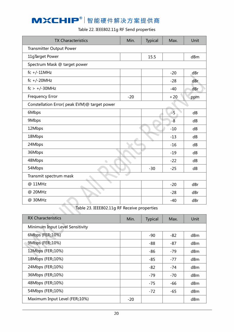
Table 22. IEEE802.11g RF Send properties
TX Characteristics Min. Typical Max. Unit
Transmitter Output Power
11gTarget Power 15.5 dBm
Spectrum Mask @ target power
fc +/-11MHz -20 dBr
fc +/-20MHz -28 dBr
fc > +/-30MHz -40 dBr
Frequency Error -20 +20 ppm
Constellation Error( peak EVM)@ target power
6Mbps -5 dB
9Mbps -8 dB
12Mbps -10 dB
18Mbps -13 dB
24Mbps -16 dB
36Mbps -19 dB
48Mbps -22 dB
54Mbps -30 -25 dB
Transmit spectrum mask
@ 11MHz -20 dBr
@ 20MHz -28 dBr
@ 30MHz -40 dBr
Table 23. IEEE802.11g RF Receive properties
RX Characteristics Min. Typical Max. Unit
Minimum Input Level Sensitivity
6Mbps (FER≦10%) -90 -82 dBm
9Mbps (FER≦10%) -88 -87 dBm
12Mbps (FER≦10%) -86 -79 dBm
18Mbps (FER≦10%) -85 -77 dBm
24Mbps (FER≦10%) -82 -74 dBm
36Mbps (FER≦10%) -79 -70 dBm
48Mbps (FER≦10%) -75 -66 dBm
54Mbps (FER≦10%) -72 -65 dBm
Maximum Input Level (FER≦10%) -20 dBm

21
3.8.4 IEEE802.11n 20MHz bandwidth mode
Table 24. IEEE802.11n RF Basic attributes
Item Specification
Modulation Type MIMO-OFDM
Channel CH1 to CH14
Data rate MCS0/1/2/3/4/5/6/7
Table 25. IEEE802.11n RF Send properties
TX Characteristics Min. Typical Max. Unit
Transmitter Output Power
11n HT20 Target Power 14.5 dBm
Spectrum Mask @ target power
fc +/-11MHz -20 dBr
fc +/-20MHz -28 dBr
fc > +/-30MHz -45 dBr
Frequency Error -25 -1.2 +25 ppm
Constellation Error( peak EVM)@ target power
MCS0 -5 dBm
MCS1 -10 dBm
MCS2 -13 dBm
MCS3 -16 dBm
MCS4 -19 dBm
MCS5 -22 dBm
MCS6 -25 dBm
MCS7 -32 -28 dBm
Transmit spectrum mask
@ 11MHz -20 dBr
@ 20MHz -28 dBr
@ 30MHz -40 dBr

22
Table 26. IEEE802.11n RF Receive properties
RX Characteristics Min. Typical Max. Unit
Minimum Input Level Sensitivity
MCS0 (FER≦10%) -89 -82 dBm
MCS1 (FER≦10%) -86 -79 dBm
MCS2 (FER≦10%) -84 -77 dBm
MCS3 (FER≦10%) -82 -74 dBm
MCS4 (FER≦10%) -78 -70 dBm
MCS5 (FER≦10%) -74 -66 dBm
MCS6 (FER≦10%) -72 -65 dBm
MCS7 (FER≦10%) -69 -64 dBm
Maximum Input Level (FER≦10%) -20 dBm

23
4 Antenna information
There is co-layout design (C35&C32) for antenna connection. Please order your module carefully.
Users can also modify the capacitor position but MXCHIP would not take any responsibility for this
behavior.
EMW3280-E load the capacitor C35 (10pF/0201), it means can use U.F.L RF connector for external
antenna. If want to use on-board PCB printed antenna, just need load the capacitor from C35 to C32
(EMW3280-P).
In order to get the maximum performance, strongly suggest customer use external antenna
connected with U.F.L RF connector.
Figure 8. Replacement antenna diagram
Minimizing radio interference 4.1
When integrating the Wi-Fi module with on board PCB printed antenna, make sure the area around
the antenna end the module protrudes at least 15mm from the mother board PCB and any metal
enclosure. If this is not possible use the on board U.FL connector to route to an external antenna.
The area (6.5mmx17.3mm) under the antenna end of the module should be keep clear of metallic
components, connectors, via, traces and other materials that can interfere with the radio signal.
15m
m
15
Figure 9. Antenna minimum clearance zone

24
U.F.L RF Connector 4.2
This module use U.F.L type RF connector for external antenna connection.
Figure 10. An external antenna connector size diagram

25
5 Mechanical Dimensions
EMW3162 Mechanical Dimensions 5.1
Figure 11. EMW3162 top view(Metric units)
Figure 12 EMW3162 side view (Metric units)
26
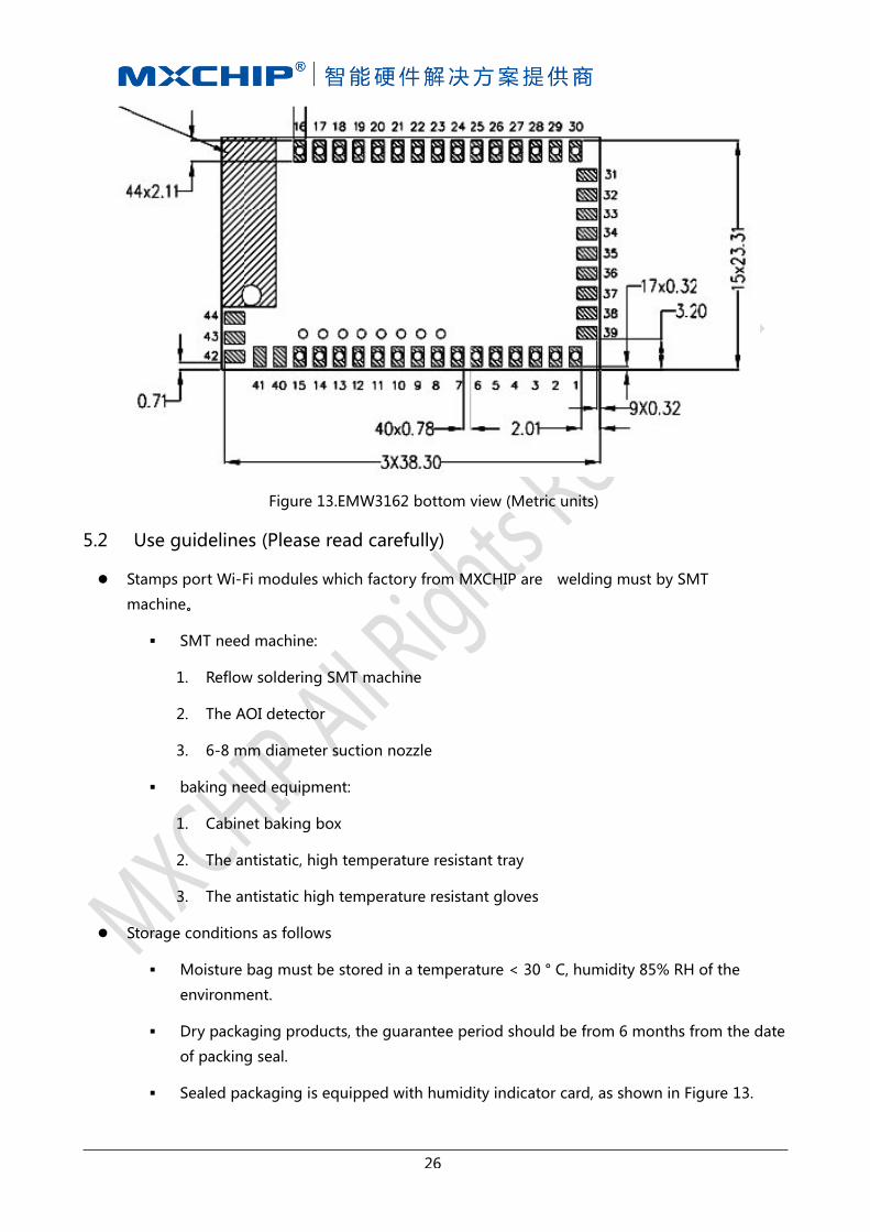
Figure 13.EMW3162 bottom view (Metric units)
Use guidelines (Please read carefully) 5.2
Stamps port Wi-Fi modules which factory from MXCHIP are welding must by SMT
machine。
SMT need machine:
1. Reflow soldering SMT machine
2. The AOI detector
3. 6-8 mm diameter suction nozzle
baking need equipment:
1. Cabinet baking box
2. The antistatic, high temperature resistant tray
3. The antistatic high temperature resistant gloves
Storage conditions as follows
Moisture bag must be stored in a temperature < 30 ° C, humidity 85% RH of the
environment.
Dry packaging products, the guarantee period should be from 6 months from the date
of packing seal.
Sealed packaging is equipped with humidity indicator card, as shown in Figure 13.

27
Humidity indicator CARDS and baking several ways as follows:
Figure 14. Temperature and humidity indicator CARDS
When opened, if the temperature and humidity indicator CARDS read 10%, 20%, 30%,40%
three color ring are blue, to continue to bake for 2 hours for module;
When opened, if the humidity indicator CARDS read 10% color ring into pink, need to
continue to bake module 4 hours;
When opened, if the humidity indicator CARDS read into 10%, 20%, color ring into pink,
need to continue to bake for 6 hours module;
When opened, if the humidity indicator CARDS read into 10%, 20%, 30% are pink color
ring, need to continue to bake for 12 hours module;
When opened, if the humidity indicator CARDS read into 10%, 20%, 30% ,40%are pink
color ring, need to continue to bake for 14 hours module;
Baking parameters are as follows:
Baking temperature: 125 + / - 5 ;
Set the alarm temperature as 130 ;
Under the condition of natural cooling < 36 , SMT placement can be made;
Dry times: 1 times;
If opened the time more than 3 months, please ban the use of SMT process welding this
batch module, zedoary because PCB process, more than 3 months bonding pad oxidation,

28
SMT is likely to cause virtual welding, welding, the resulting problems we do not assume
corresponding responsibility.
Please to ESD(static discharge,static electricity discharge) protection module before
SMT;
Please according to the SMT reflow soldering curve, peak temperature 245 , reflow
soldering temperature curve as shown in figure 14, section 7.6;
For the first time in order to ensure the qualified rate of reflow soldering, first SMT please
extraction 10% product to visual analysis, AOI inspection, to ensure that the furnace
temperature control, device adsorption method, the rationality of the put way;
Suggestions:when batch production per hour 5-10 pieces of visual analysis, AOI test;
The matters needing attention 5.3
In the entire production, Each station of the operator must wear anti-static gloves;
When baking, no more than baking time;
When roasting, it is forbidden to join explosive, flammable, corrosive substances;
When baking, high temperature module application tray in the oven, keep the air
circulation between each module, at the same time avoid direct contact with the oven
wall module;
Baking, please will bake the door is closed, the guarantee baking box sealing, prevent
leakage, temperature influence the baking effect;
Don't open the door, as far as possible when baking box running if must open, shortening
the time of can open the door as far as possible;
After baking, must be natural cooling modules to < 36 before wear anti-static gloves
out, so as not to burn.
Operation, forbidden module bottom touch water or dirt;
Temperature and humidity control level for Level3, storage and baking conditions based
on IPC/JEDEC J - STD - 020.
29
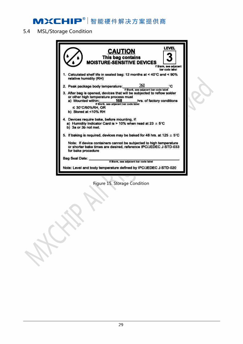
MSL/Storage Condition 5.4
Figure 15. Storage Condition

30
Recommended Reflow Profile 5.5
Reflow times<= 2times (Max.)
Figure 16 . Temperature Curve

31
6 Reference circuit
EMW3162 user reference circuit is as follows:
Figure 16-the power reference circuit, Figure 17-USB to serial reference circuit, Figure 18-module
refer to the external interface circuit.
Figure 17. Power reference circuit
Figure 18. USB to serial reference circuit

32
Figure 19. Module refer to the external interface circuit

33
7 5 V UART - 3.3V UART conversion reference circuit
EMW3162 UART is 3.3 V, if the user use UART chip is 5 V, the need to convert the voltage, can with
EMW3162 UART communication, please refer to the 5 V to 3.3 V UART conversion circuit Figure 19.
Figure 20. UART 5 V - 3.3 V conversion circuit
34
8 Sales Information and Technical Support
If you need to get the latest information on this product or our other product information, you can
visit: http://www.mxchip.com/.
If you need to get technical support, please call us during the working hours.
From Monday to Friday, morning 9:00~12:00, afternoon 13:00~18:00
Telephone: +86 (021)52655026-822
Email: [email protected]
Postcode: 200333
Contact address: Room 811, Tongpu Building, No.1220, and Tongpu Road, Shanghai, China

35
9 Version Update Instructions
Data Revision Changes
2015-08-05 V2.4
1. Update 2.2 recommended package
2. Update section 4.1 antenna type
3. Add section 5.2 production Guide
(Please read carefully)
4. increased 5.3 considerations
5. add a 6th chapter reference circuit
6. Increase chapter 7 the UART 5 V - 3.3 V
UART conversion reference circuit
2016-3-14 V2.5
Update the mechanical Dimensions