data retention in mlc nand flash memory: …yixinluo/index_files/data-retention_fms15.pdf · in mlc...
TRANSCRIPT

Data Retention in MLC NAND Flash Memory: Characterization,
Optimization, and RecoveryYixin Luo
[email protected](joint work with Yu Cai, Erich F. Haratsch, Ken Mai, Onur Mutlu)
1
Presented in the best paper session at HPCA 2015

2
Characterize
Recover
Optimize
retention loss in real NAND chip
read performance for old data
old data after failure

3
read performance degradation
old filesas slow as 30MB/s newly-written files
500 MB/s
Reference: (May 5, 2015) Per Hansson, “When SSD Performance Goes Awry” http://www.techspot.com/article/997-samsung-ssd-read-performance-degradation/

4
Why is old data slower?
Retention loss!
Image source: http://tinyurl.com/ng2gfg9

Retention loss
5
Charge leakage over time
One dominant source of flash memory errors [DATE ‘12, ICCD ‘12]
Retention error
Flash cell Flash cell Flash cell
Side effect: Longer read latency

Multi-Level Cell (MLC)threshold voltage distribution
6
Normalized Vth
Erased(11)
P1(10)
P2(00)
P3(01)
Va Vb Vc

Experimental Testing Platform
USB Jack
Virtex-II Pro
(USB controller)
Virtex-V FPGA
(NAND Controller)
HAPS-52 Mother Board
USB Daughter Board
NAND Daughter Board
3x-nm
NAND Flash
[Cai+, FCCM 2011, DATE 2012, ICCD 2012, DATE 2013, ITJ
2013, ICCD 2013, SIGMETRICS 2014, DSN 2015, HPCA 2015]
Cai et al., FPGA-based Solid-State Drive prototyping platform, FCCM 2011. 7
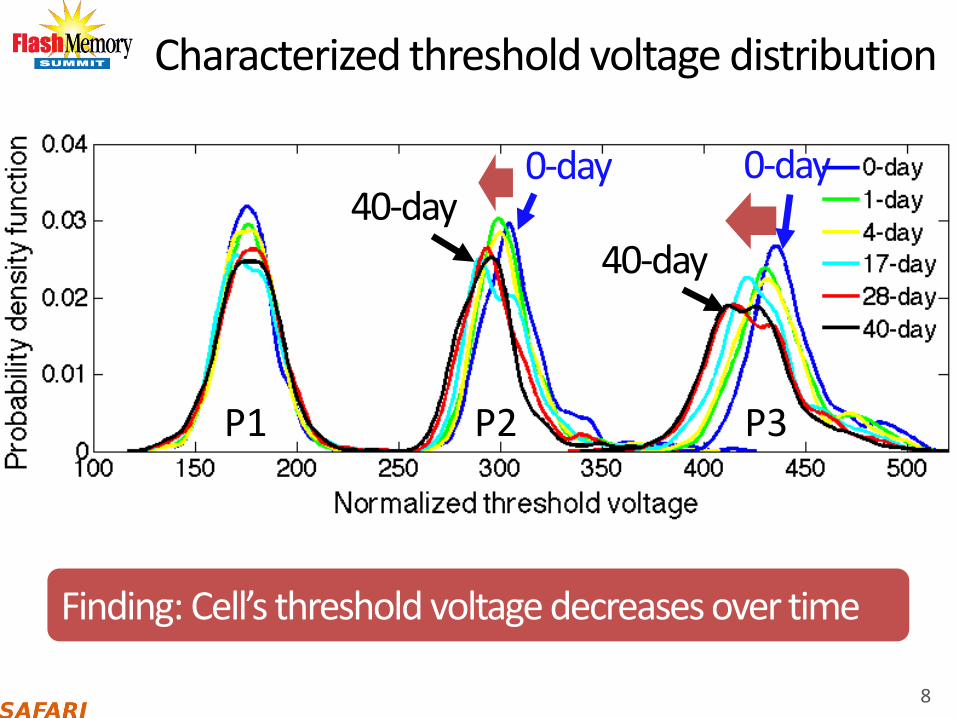
Characterized threshold voltage distribution
8
Finding: Cell’s threshold voltage decreases over time
P1 P2 P3
0-day
40-day
0-day40-day

9
Normalized Vth
P1(10)
P2(00)
P3(01)
New dataOld data
Threshold voltage reduces over time
More charge
Less charge

First read attempt fails
10
Normalized Vth
Vb Vc
Normalized Vth
Raw bit errors > ECC correctable errors
Old data
P1(10)
P2(00)
P3(01)
More charge
Less charge

Read-retry
11
Normalized Vth
Vb VcVb’ Vc’
Fewer raw bit errors
Old data
P1(10)
P2(00)
P3(01)
Increase read latency

Why is old data slower?
Retention loss
Leak charge over time
Generate retention errors
Require read-retry
Longer read latency
12

13
Characterize
Recover
Optimize
retention loss in real NAND chip
read performance for old data
old data after failure

The ideal read voltage
14
Normalized Vth
OPTb OPTc
Minimal raw bit errors
Old data
P1(10)
P2(00)
P3(01)
OPT: Optimal read reference voltageminimal read latency

In reality
•OPT changes over time due to retention loss
•Luckily, OPT change is:‐ Gradual‐ Uni-directional (decrease over time)
15

Retention Optimized Reading (ROR)
Components:
1. Online pre-optimization algorithm‐ Learns and records OPT‐ Performs in the background once every day
2. Simpler read-retry technique‐ If recorded OPT is out-of-date, read-retry with lower voltage
16

ROR result
17
Total read latency, 29%
BCH decoding latency, 90%
Read-retry count, 30%
0% 20% 40% 60% 80% 100%
Tota
l rea
dla
ten
cy
BC
Hd
eco
din
gla
ten
cyR
ead
-ret
ryco
un
tBaseline ROR

Retention optimized reading
Retention loss longer read latency
Optimal read reference voltage (OPT)
Shortest read latency
Decreases gradually over time (retention)
Learn OPT periodically
Minimize read-retry & RBER
Shorter read latency
18

19
Characterize
Recover
Optimize
retention loss in real NAND chip
read performance for old data
old data after failure

Correctable errors
Retention failure
20
Normalized Vth
PDFP1
(10)P2
(00)P3
(01)OPTb OPTc
Uncorrectable errors
Old dataVery old data

Leakage speed variation
21
Normalized Vth
S
F
low-leaking cell
ast-leaking cell
S
F
N-day retention
N-day retention

A simplified example
22
Normalized Vth
S
F
SF
S
F
SF
P2 P3

Very old data
P2 P3
F
F
F
F
Reading very old data
23
Normalized Vth
S
F
SF
S
F
SF
Fast-leaking cells have lower Vth
Slow-leaking cells have higher Vth

“Risky” cells
24
Normalized Vth
S
S
F
F
OPT OP
T+σ
OP
T–σ
Risky cells
P2
P3
+ S =
+ F =
Key Formula
Uncorrectable errors

Retention Failure Recovery (RFR)
Key idea: Guess original state of the cell from its leakage speed property
Three steps
1. Identify risky cells
2. Identify fast-/slow-leaking cells
3. Guess original states
25
Risky cells
P2
P3
+ S =
+ F =
Key Formula
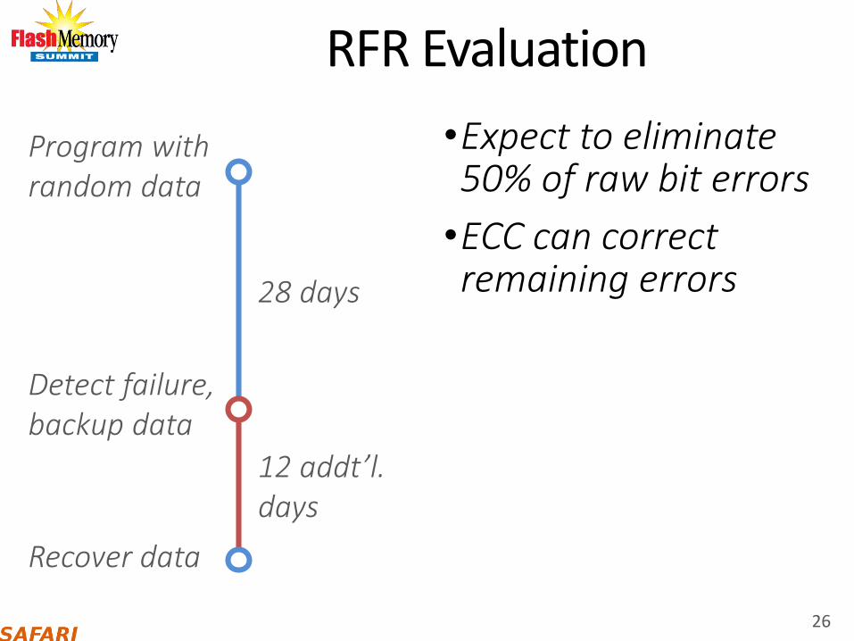
RFR Evaluation
•Expect to eliminate 50% of raw bit errors
•ECC can correct remaining errors
26
Program with random data
Detect failure, backup data
Recover data
28 days
12 addt’l. days

27
Characterize
Recover
Optimize
retention loss in real NAND chip
read performance for old data
old data after failure

Conclusion
Retention loss Longer read latency
Retention optimized reading (ROR)
Learns OPT periodically
71% shorter read latency
Retention failure recovery (RFR)
Use leakage property to guess correct state
50% error reduction before ECC correction
Recover data after failure
28

Our FMS Talks and Posters•Onur Mutlu, Error Analysis and Management for MLC
NAND Flash Memory, FMS 2014.
•Onur Mutlu, Read Disturb Errors in MLC NAND Flash Memory, FMS 2015.
• Yixin Luo, Data Retention in MLC NAND Flash Memory, FMS 2015.
• FMS 2015 posters:‐ WARM: Improving NAND Flash Memory Lifetime with Write-
hotness Aware Retention Management‐ Read Disturb Errors in MLC NAND Flash Memory‐ Data Retention in MLC NAND Flash Memory
29

Our Flash Memory Works (I)
1. Retention noise study and management1) Yu Cai, Gulay Yalcin, Onur Mutlu, Erich F. Haratsch, Adrian Cristal, Osman
Unsal, and Ken Mai, Flash Correct-and-Refresh: Retention-Aware Error Management for Increased Flash Memory Lifetime, ICCD 2012.
2) Yu Cai, Yixin Luo, Erich F. Haratsch, Ken Mai, and Onur Mutlu, Data Retention in MLC NAND Flash Memory: Characterization, Optimization and Recovery, HPCA 2015.
3) Yixin Luo, Yu Cai, Saugata Ghose, Jongmoo Choi, and Onur Mutlu, WARM: Improving NAND Flash Memory Lifetime with Write-hotness Aware Retention Management, MSST 2015.
2. Flash-based SSD prototyping and testing platform4) Yu Cai, Erich F. Haratsh, Mark McCartney, Ken Mai, FPGA-based solid-state
drive prototyping platform, FCCM 2011.
30

Our Flash Memory Works (II)
3. Overall flash error analysis5) Yu Cai, Erich F. Haratsch, Onur Mutlu, and Ken Mai, Error Patterns in MLC
NAND Flash Memory: Measurement, Characterization, and Analysis, DATE 2012.
6) Yu Cai, Gulay Yalcin, Onur Mutlu, Erich F. Haratsch, Adrian Cristal, Osman Unsal, and Ken Mai, Error Analysis and Retention-Aware Error Management for NAND Flash Memory, ITJ 2013.
4. Program and erase noise study7) Yu Cai, Erich F. Haratsch, Onur Mutlu, and Ken Mai, Threshold Voltage
Distribution in MLC NAND Flash Memory: Characterization, Analysis and Modeling, DATE 2013.
31

Our Flash Memory Works (III)5. Cell-to-cell interference characterization and tolerance
8) Yu Cai, Onur Mutlu, Erich F. Haratsch, and Ken Mai, Program Interference in MLC NAND Flash Memory: Characterization, Modeling, and Mitigation, ICCD 2013.
9) Yu Cai, Gulay Yalcin, Onur Mutlu, Erich F. Haratsch, Osman Unsal, Adrian Cristal, and Ken Mai, Neighbor-Cell Assisted Error Correction for MLC NAND Flash Memories, SIGMETRICS 2014.
6. Read disturb noise study10) Yu Cai, Yixin Luo, Saugata Ghose, Erich F. Haratsch, Ken Mai, and Onur Mutlu,
Read Disturb Errors in MLC NAND Flash Memory: Characterization and Mitigation, DSN 2015.
7. Flash errors in the field11) Justin Meza, Qiang Wu, Sanjeev Kumar, and Onur Mutlu, A Large-Scale Study
of Flash Memory Errors in the Field, SIGMETRICS 2015.
32

Referenced Papers and Talks
•All are available athttp://users.ece.cmu.edu/~omutlu/projects.htm
33

Thank you!Feel free to email me with any questions & feedback
http://www.cs.cmu.edu/~yixinluo
34

Data Retention in MLC NAND Flash Memory: Characterization,
Optimization, and RecoveryYixin Luo
[email protected](joint work with Yu Cai, Erich F. Haratsch, Ken Mai, Onur Mutlu)
35

Backup Slides
36

ROR overheads
•Power-on latency: 3, 15, and 23 seconds for flash memory with 1-day, 7-day, and 30-day equivalent retention age
•Per-day pre-optimization latency: 3 seconds
•Total storage overhead: 768 KB
37

Attempt 2
Read-Retry Latency Diagnosis
38
Attempt 1time
Read page A:
Flash Read Latency ECC Latency
= Constant ∝ Raw bit error
Attempt 3

ROR assumptions
•We model a 512 GB flash-based SSD (composed of sixteen 256 Gbit flash memory chips) with an 8 KB page size, 256-page block size, and 100 μs read latency.
•We model a flash controller with an iterative BCH decoder that can correct 40 bit errors for every 1 KB of data [11] (i.e., it can tolerate an RBER of 10-3 during the flash lifetime).
39

RFR Motivation
Data loss can happen in many ways
1. High P/E cycle
2. High temperature accelerates retention loss
3. High retention age (lost power for a long time)
40

What if there are other errors?
Key: RFR does not have to correct all errors
Example:
•ECC can correct 40 errors in a page
•Corrupted page has 20 retention errors, 25 other errors (45 total errors)
•After RFR: 10 retention errors, 30 other errors (40 total errors ECC correctable)
41

Characterization methodology
•FPGA-based flash memory testing platform
•Real 20- to 24-nm MLC NAND flash chips
•0- to 40-day worth of retention loss
•Room temperature (20⁰C)
•0 to 50k P/E Cycles
42

Firmware fix
43

Firmware fix
44

Optimal Read Reference Voltage (OPT)
45
P1 P2 P3
Finding: OPT decreases over time
0-day OPT
40-day OPT
0-day OPT
40-day OPT

Retention Optimized Reading: Summary
46
Flash Read Techniques
Lifetime(P/E Cycle)
Performance(Read Latency)
Fixed Vref
Sweeping Vref
64% ↑
ROR 64% ↑ _____Nom. Life: 2.4% ↓
Ext. Life: 70.4% ↓

1. The optimal read reference voltage gradually decreases over time
Key idea: Record the old OPT as a prediction (Vpred) of the actual OPT
Benefit: Close to actual OPT Fewer read retries
2. The amount of retention loss is similar across pages within a flash block
Key idea: Record only one Vpred for each block
Benefit: Small storage overhead (768KB out of 512GB)
Observations
47

1. Online Pre-Optimization Algorithm
•Triggered periodically (e.g., per day)
•Find and record an OPT as per-block Vpred
•Performed in background
•Small storage overhead
48
Normalized Vth
PDFNew Vpred
Old Vpred

2. Improved Read-Retry Technique
•Performed as normal read
•Vpred already close to actual OPT
•Decrease Vref if Vpred fails, and retry
49
Normalized Vth
PDF OPT Vpred
Very close

1. Identify Risky Cells
50
Normalized Vth
S
S
F
F
OP
T+σ
OP
T
OP
T–σ
Risky cells
P2
P3
+ S =
+ F =
Key Formula

2. Identifying Fast- vs. Slow-Leaking Cells
51
Normalized Vth
OP
T+σ
OP
T
OP
T–σ
Risky cells
P2
P3
+ S =
+ F =
Key Formula
?
?
?
?
?
?

2. Identifying Fast- vs. Slow-Leaking Cells
52
Normalized Vth
OP
T+σ
OP
T
OP
T–σ
Risky cells
P2
P3
+ S =
+ F =
Key Formula
?
?
?
?
S F
F S
?
?

3. Guess Original States
53
Normalized Vth
S F
F S
Risky cells
P2
P3
+ S =
+ F =
Key Formula

Actual OPT
Reading data with 7-day worth of retention loss.
3. RBER and P/E Cycle Lifetime
54
ECC-correctable RBER
Finding: Using actual OPT achieves the longest lifetime
Vref closer to actual OPT
No
min
al
Life
tim
e
Exte
nd
ed
Life
tim
e

Characterization Summary
Due to retention loss‐ Cell’s threshold voltage (Vth) decreases over time‐ Optimal read reference voltage (OPT) decreases over time
Using the actual OPT for reading‐ Achieves the longest lifetime
55

Threshold Voltage (Vth) Mean
56
Thre
sho
ld v
olt
age
me
an
P1 P2 P3
Finding: Vth shifts faster in higher voltage states
Quickly decrease
Slowly decrease
Relatively constant

Raw Bit Error Rate (RBER)
57
Actual OPT
Reading data with 7-day retention age.
Finding: The actual OPT achieves the lowest RBER
RBER gradually decreases as read reference voltage approaches the actual OPT
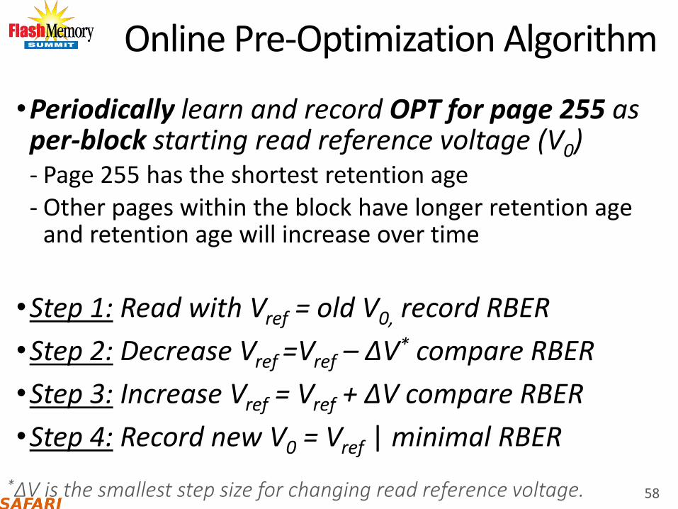
Online Pre-Optimization Algorithm
•Periodically learn and record OPT for page 255 as per-block starting read reference voltage (V0)‐ Page 255 has the shortest retention age‐ Other pages within the block have longer retention age
and retention age will increase over time
•Step 1: Read with Vref = old V0, record RBER
•Step 2: Decrease Vref =Vref – ΔV* compare RBER
•Step 3: Increase Vref = Vref + ΔV compare RBER
•Step 4: Record new V0 = Vref | minimal RBER
58*ΔV is the smallest step size for changing read reference voltage.

Arrhenius Law
59
1 year
32 hours
Room temperature (20°C)
High temperature (70°C)
High temperature accelerates retention loss

Fast- and Slow-Leaking Cells
60
Slow-leaking cells
Fast-leaking cells
(-1σ,μ)
(1σ,2σ)
(2σ,3σ)
(3σ,+∞)
(-∞,-3σ)
(-3σ,-2σ)
(-2σ,-1σ)
(μ,1σ)
Retention age (days)*Similar trends are found in P2 state, as shown in the paper.
Ave
rage
Vth
shif
t
Ends up in higher Vth
Ends up in higher Vth

Fast- and Slow-Leaking Cells
61
Normalized Vth
PDFμ 1σ 2σ 3σ-3σ -2σ -1σ
Threshold voltage marks after 28 days:

Fast- and Slow-Leaking Cells
62
Slow-leaking cells
Fast-leaking cells
(-1σ,μ)
(1σ,2σ)
(2σ,3σ)
(3σ,+∞)
(-∞,-3σ)
(-3σ,-2σ)
(-2σ,-1σ)
(μ,1σ)
Retention age (days)*Similar trends are found in P2 state, as shown in the paper.
Ave
rage
Vth
shif
t
Ends up in higher Vth
Ends up in lower Vth

63
Substrate
Floating gate (FG)
Control gate (CG)
DrainSource
Inter-poly oxide
Tunnel oxide
Substrate
FG
CG
DS