data brief - x-nucleo-iod02a1 - dual channel io-link
TRANSCRIPT
Features• Based on the L6364Q IO-Link device dual transceiver in QFN package with the
following main characteristics:– 2-channel (CQ and DIO) IO-Link PHY layer– IO-Link DLL (M-sequence handler and checksum)– Wake-up detection– Interrupt diagnostic pin– SPI and UART interfaces– 50 mA 3.3 V and 5.0 V linear regulators– 50 mA adjustable (5.0 ÷ 10.8 V) buck converter– Overload protection with adjustable intervention threshold– Overheating protection with adjustable shutdown threshold– Full reverse polarity on process side– Ground and VCC wire break protections– QFN-20L (4 x 4 x 0.9 mm) package
• 5 to 35 V operating voltage range• Red LED and green LED for status diagnostics• Radiated Emissions (EM Fields 30 MHz-1 GHz) < 40dB µV/m• Immunity to conducted disturbance (150 kHz-80 MHz) ≤ 10 V• Immunity to RF EM Fields (80 MHz-1 GHz) ≤ 10 V/m• Immunity to RF EM Fields (1 GHz-2.7 GHz) ≤ 3 V/m• Immunity to SURGE pulse (500 Ohm coupling) ≤ ± 1.2 kV• Immunity to ESD contact/air ≤ ±3 kV• Immunity to BURST noise ≤ ±1 kV• Compatible with STM32 Nucleo development boards• Equipped with Arduino UNO R3 connectors• RoHS and WEEE compliant
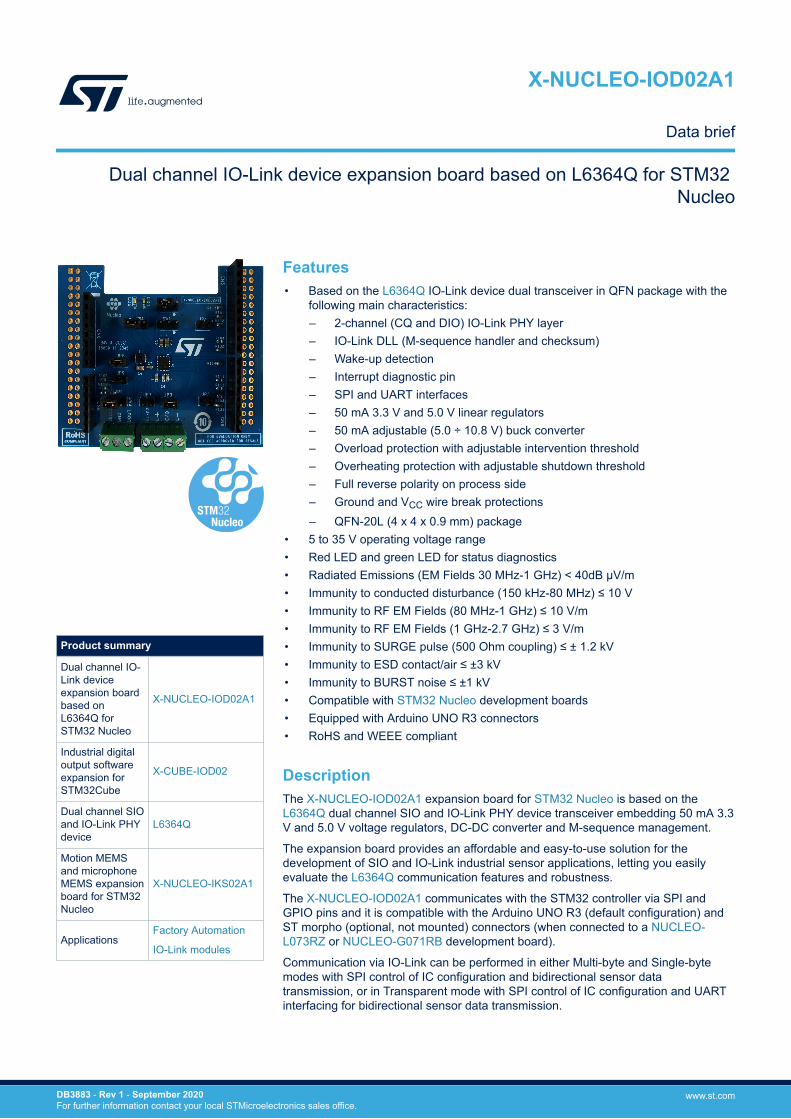
DescriptionThe X-NUCLEO-IOD02A1 expansion board for STM32 Nucleo is based on theL6364Q dual channel SIO and IO-Link PHY device transceiver embedding 50 mA 3.3V and 5.0 V voltage regulators, DC-DC converter and M-sequence management.
The expansion board provides an affordable and easy-to-use solution for thedevelopment of SIO and IO-Link industrial sensor applications, letting you easilyevaluate the L6364Q communication features and robustness.
The X-NUCLEO-IOD02A1 communicates with the STM32 controller via SPI andGPIO pins and it is compatible with the Arduino UNO R3 (default configuration) andST morpho (optional, not mounted) connectors (when connected to a NUCLEO-L073RZ or NUCLEO-G071RB development board).
Communication via IO-Link can be performed in either Multi-byte and Single-bytemodes with SPI control of IC configuration and bidirectional sensor datatransmission, or in Transparent mode with SPI control of IC configuration and UARTinterfacing for bidirectional sensor data transmission.
Product summary
Dual channel IO-Link deviceexpansion boardbased onL6364Q forSTM32 Nucleo
X-NUCLEO-IOD02A1
Industrial digitaloutput softwareexpansion forSTM32Cube
X-CUBE-IOD02
Dual channel SIOand IO-Link PHYdevice
L6364Q
Motion MEMSand microphoneMEMS expansionboard for STM32Nucleo
X-NUCLEO-IKS02A1
ApplicationsFactory Automation
IO-Link modules
Dual channel IO-Link device expansion board based on L6364Q for STM32 Nucleo
X-NUCLEO-IOD02A1
Data brief
DB3883 - Rev 1 - September 2020For further information contact your local STMicroelectronics sales office.
www.st.com

The switches on the X-NUCLEO-IOD02A1 conveniently allow you to configureL6364Q and expansion board settings such as transmission mode and DC-DCconverter enable/disable according to application requirements.
You can also perform evaluation of comprehensive industrial sensor modules byconnecting the X-NUCLEO-IOD02A1 to the X-NUCLEO-IKS02A1 sensor shield.
X-NUCLEO-IOD02A1
DB3883 - Rev 1 page 2/6

1 Schematic diagrams
Figure 1. X-NUCLEO-IOD02A1 circuit schematic (1 of 2)
INT
JP3
PB8
PA9
(Note: I2C_SCL)(Note: I2C_SDA)
PA6PA7
PA8
(Note: UART2 TX, ST-LINK)(Note: UART2 RX, ST-LINK)
100 N.M.
CN5
2022
100
28
10
VIN
SS
38
4
11
100
CN9
2121
CQ
29
DIO
1
31
13
34
8
default open
CN6
28
7
13
CTLD
IOREF
L-DI/DQ/2L+
1
SCLK
NRST
R103
2
N.M.
MISO
DEFAULTALTERNATE
DEFAULT
DEFAULT
8
R105
5
107
MISO
5
7
VIN
100 N.M.
R104
9
R117
3
3
20
GND
12
100 N.M.
UART(RX)
1
6
37
MOSI
ALTERNATE
11
SSQ-119-04-L-D
2
MOSI
2
VCC
100
JP7
38
26
100 N.M.JP4
17
5
4
33
GND
12
16
100
2
1
CN3
CN2
7
DEFAULTDEFAULT
PA4PB0
ALTERNATE
CN9(3)
PA0 ALTERNATEPA1
PC0PC1
6
SSQ-108-04-F-S
31
MISO
SS
8
ALTERNATE
CN1
INT
1
MISO
CTLD
18
37
14
9
6
SSQ-119-04-L-D
7
3332
5
L+
9
32
3
JP5VIN
13
SSQ-108-04-F-S
4
3
PA10
22
17
36
30
default openR112
3V3
16
2
24
1
UART(TX)
24
2
MOSI
3
35
30
SSSS
35
CN7
default open
R131
1
19
CN8
100
27
VDCDC
6
23
100 N.M.
100
26
INT
4
15
AVDD
SSQ-110-04-F-S
225
4
R102
MOSI
27
JP9
2
N.M.
2
36
1
100
3V3
INT
C/Q
PA3
PC7PB6
PB5
PA5
23
CN10
PB4PB10
PB3
PB9
PA2
10
6
18
default closed
R132
SCLK5
default open
R113
25
8
5V
8
SCLK
29
34
R114
3
CTLDSCLK
R115R111
DOUTR101
14
Arduino Connectors
Morpho Connectors IO-Link Device supply voltage 7 V - 36 V
5 100
UART(RX)
4
5V
19
SSQ-106-04-F-S
15
6
DB
3883 - Rev 1
page 3/6
X-NU
CLEO
-IOD
02A1
Schematic diagram
s

Figure 2. X-NUCLEO-IOD02A1 circuit schematic (2 of 2)
CQ
PGN
D
16
default CLOSE1-2
VIN
SW1
DIO
LOUT
The dc-dc of L6364 supplies the nucleo by Vin net(CN6[8])
DOUT
DIO
10nF
VDIG
SW2
SW3
CTLD_PIN
C6
GND_TAB
1
4G
ND
3
470pF
VCC
5V
CTLD
MOSI17
4.7k
V5V
CTLD_PIN
VDCDC
115
5BC
12
CQ
SCK
23V3
LD1default CLOSE1-2
INT
6LED1
VDC
DC
VIN
CTLD
21
default CLOSE1-21
C
C3
3
20
VDCDC
CSS 7
LED2
V3V3
LOUT
9DOUT
0.22uF
U1
LED GREEN
R20
default closed
C2
MISOC7
470pF
C5
RED LED
SCLK
C1
2
1
1
L636411VP
LUS
DIO
220uH
A
3
L1
2
default ALL open
3
MISO
3V3 and 5V generated on the STM32 Nucleo board from Vin
8MOSI
VDIG
2
SW4
A
4.7uF
10
JP8
VDCDC
13C
Q14
LD2
2
1
C4
2
4.7uF
DOUT
INT
2.2uF
18
SS19
V3V3
3V5
V
DB
3883 - Rev 1
page 4/6
X-NU
CLEO
-IOD
02A1
Schematic diagram
s

Revision history
Table 1. Document revision history
Date Version Changes
01-Sep-2020 1 Initial release.
X-NUCLEO-IOD02A1
DB3883 - Rev 1 page 5/6

IMPORTANT NOTICE – PLEASE READ CAREFULLY
STMicroelectronics NV and its subsidiaries (“ST”) reserve the right to make changes, corrections, enhancements, modifications, and improvements to STproducts and/or to this document at any time without notice. Purchasers should obtain the latest relevant information on ST products before placing orders. STproducts are sold pursuant to ST’s terms and conditions of sale in place at the time of order acknowledgement.
Purchasers are solely responsible for the choice, selection, and use of ST products and ST assumes no liability for application assistance or the design ofPurchasers’ products.
No license, express or implied, to any intellectual property right is granted by ST herein.
Resale of ST products with provisions different from the information set forth herein shall void any warranty granted by ST for such product.
ST and the ST logo are trademarks of ST. For additional information about ST trademarks, please refer to www.st.com/trademarks. All other product or servicenames are the property of their respective owners.
Information in this document supersedes and replaces information previously supplied in any prior versions of this document.
© 2020 STMicroelectronics – All rights reserved
X-NUCLEO-IOD02A1
DB3883 - Rev 1 page 6/6