dac8811 16-bit, serial input multiplying digital-to … · d/a converter power-on reset dac...
TRANSCRIPT

D/A
Converter
Power-OnReset
DAC
Register
Shift
Register
16
16
RFB
IOUT
GND
VDD
VREF
CS
CLK
SDI
DAC8811
Product
Folder
Sample &Buy
Technical
Documents
Tools &
Software
Support &Community
An IMPORTANT NOTICE at the end of this data sheet addresses availability, warranty, changes, use in safety-critical applications,intellectual property matters and other important disclaimers. PRODUCTION DATA.
DAC8811SLAS411D –NOVEMBER 2004–REVISED FEBRUARY 2016
DAC8811 16-Bit, Serial Input Multiplying Digital-to-Analog Converter
1
1 Features1• ±0.5 LSB DNL• 16-Bit Monotonic• ±1 LSB INL• Low Noise: 12 nV/√Hz• Low Power: IDD = 2 µA• 2.7-V to 5.5-V Analog Power Supply• 2-mA Full-Scale Current ±20%,
with VREF = 10 V• 50-MHz Serial Interface• 0.5-μs Settling Time• 4-Quadrant Multiplying Reference• Reference Bandwidth: 10 MHz• ±10-V Reference Input• Reference Dynamics: –105 THD• Tiny 8-Lead 3 × 3 mm VSON and 3 × 5 mm
VSSOP Packages• Industry-Standard Pin Configuration
2 Applications• Automatic Test Equipment• Instrumentation• Digitally Controlled Calibration• Industrial Control PLCs
3 DescriptionThe DAC8811 multiplying digital-to-analog converter(DAC) is designed to operate from a single 2.7-V to5.5-V supply.
The applied external reference input voltage VREFdetermines the full-scale output current. An internalfeedback resistor (RFB) provides temperature trackingfor the full-scale output when combined with anexternal I-to-V precision amplifier.
A serial data interface offers high-speed, three-wiremicrocontroller-compatible inputs using data-in (SDI),clock (CLK), and chip-select (CS).
On power-up, the DAC register is filled with zeroes,and the DAC output is at zero scale.
The DAC8811 is packaged in space-saving 8-leadVSON and VSSOP packages.
Device Information(1)
PART NUMBER PACKAGE BODY SIZE (NOM)
DAC8811VSSOP (8) 3.00 mm × 3.00 mmVSON (8) 3.00 mm × 3.00 mm
(1) For all available packages, see the orderable addendum atthe end of the datasheet.
Simplified Schematic

2
DAC8811SLAS411D –NOVEMBER 2004–REVISED FEBRUARY 2016 www.ti.com
Product Folder Links: DAC8811
Submit Documentation Feedback Copyright © 2004–2016, Texas Instruments Incorporated
Table of Contents1 Features .................................................................. 12 Applications ........................................................... 13 Description ............................................................. 14 Revision History..................................................... 25 Device Comparison Table ..................................... 46 Pin Configuration and Functions ......................... 47 Specifications......................................................... 5
7.1 Absolute Maximum Ratings ..................................... 57.2 ESD Ratings ............................................................ 57.3 Recommended Operating Conditions....................... 57.4 Thermal Information .................................................. 57.5 Electrical Characteristics........................................... 67.6 Timing Requirements ................................................ 77.7 Typical Characteristics: VDD = 5 V........................... 87.8 Typical Characteristics: VDD = 2.7 V...................... 10
8 Detailed Description ............................................ 118.1 Overview ................................................................ 118.2 Functional Block Diagram ....................................... 11
8.3 Feature Description................................................. 118.4 Device Functional Mode ......................................... 148.5 Programming........................................................... 15
9 Application and Implementation ........................ 169.1 Application Information............................................ 169.2 Typical Application ................................................. 16
10 Power Supply Recommendations ..................... 1711 Layout................................................................... 18
11.1 Layout Guidelines ................................................. 1811.2 Layout Example .................................................... 18
12 Device and Documentation Support ................. 1912.1 Documentation Support ........................................ 1912.2 Community Resources.......................................... 1912.3 Trademarks ........................................................... 1912.4 Electrostatic Discharge Caution............................ 1912.5 Glossary ................................................................ 19
13 Mechanical, Packaging, and OrderableInformation ........................................................... 19
4 Revision HistoryNOTE: Page numbers for previous revisions may differ from page numbers in the current version.
Changes from Revision C (October 2015) to Revision D Page
• Changed the DAC8811 Timing Diagram image to show the setup and hold time with respect to rising edge .................... 7• Changed two instances of falling to rising in the DAC8811 Input Shift Register section ..................................................... 15• Changed the SYNC Interrupt Facility image ........................................................................................................................ 15
Changes from Revision B (February 2007) to Revision C Page
• Added ESD Ratings table, Recommended Operating Conditions table, Thermal Information table, TimingRequirements table, Feature Description section, Device Functional Modes, Application and Implementation section,Power Supply Recommendations section, Layout section, Device and Documentation Support section, andMechanical, Packaging, and Orderable Information sections. .............................................................................................. 1
• Changed R3' From: 50 kΩ To: 50 Ω in Figure 23 ................................................................................................................ 14
Changes from Revision A (December 2004) to Revision B Page
• Added a new paragraph to the Description , "On power-up,..." ............................................................................................. 1• Changed the Simplified Schematic to include the Power-On Reset ...................................................................................... 1• Added VREF, RFB to GND to the Absolute Maximum Ratings ................................................................................................ 5• Changed the ESD rating of HBM From: 1500 To: 4000 in the Absolute Maximum Ratings ................................................ 5• Added table note: " All ac characteristic tests are performed.." to the Electrical Characteristics........................................... 6• Added test conditions to the Output voltage settling time of the AC characteristics section in the Timing
Requirements ........................................................................................................................................................................ 7• Added table note: " All ac characteristic tests are performed.." to the Electrical Characteristics........................................... 7• Changed Figure 9................................................................................................................................................................... 8

3
DAC8811www.ti.com SLAS411D –NOVEMBER 2004–REVISED FEBRUARY 2016
Product Folder Links: DAC8811
Submit Documentation FeedbackCopyright © 2004–2016, Texas Instruments Incorporated
Changes from Original (November 2004) to Revision A Page
• Removed the Product Preview label ...................................................................................................................................... 1• Added information to the Features ........................................................................................................................................ 1• Added Output leakage current Data = 0000h, TA = TMAX in the Electrical Characteristics .................................................... 6• Added Input high voltage for VDD = 2.7 V and 2.5 V in the Electrical Characteristics ........................................................... 6• Changed the values of the Power Requirements and the AC characteristics section in the Electrical Characteristics ....... 6

1
2
3
4
8
7
6
5
CLK
SDI
RFB
VREF
CS
VDD
GND
IOUT
CLK
SDI
RFB
VREF
CS
VDD
GND
IOUT
1
2
3
4
8
7
6
5
4
DAC8811SLAS411D –NOVEMBER 2004–REVISED FEBRUARY 2016 www.ti.com
Product Folder Links: DAC8811
Submit Documentation Feedback Copyright © 2004–2016, Texas Instruments Incorporated
5 Device Comparison Table
PART NUMBER INL (LSB) DNL (LSB)DAC8811ICDGK ±1 ±1DAC8811IBDGK ±2 ±1DAC8811ICDRB ±1 ±1DAC8811IBDRB ±2 ±1
6 Pin Configuration and Functions
DRB Package8-Pins VSON
Top View
DGK Package8-Pins VSSOP
Top View
Pin FunctionsPIN
TYPE DESCRIPTIONNAME NO.
CLK 1 I Clock input; positive edge triggered clocks data into shift register
SDI 2 I Serial register input; data loads directly into the shift register MSB first. Extra leading bits areignored.
RFB 3 O Internal matching feedback resistor. Connect to external op amp output.
VREF 4 I DAC reference input pin. Establishes DAC full-scale voltage. Constant input resistance versuscode.
IOUT 5 O DAC current output. Connects to inverting terminal of external precision I/V op amp.GND 6 G Analog and digital ground.VDD 7 I Positive power supply input. Specified operating range of 2.7 V to 5.5 V.
CS 8 I Chip-select; active low digital input. Transfers shift register data to DAC register on rising edge.See Table 1 for operation.
5
DAC8811www.ti.com SLAS411D –NOVEMBER 2004–REVISED FEBRUARY 2016
Product Folder Links: DAC8811
Submit Documentation FeedbackCopyright © 2004–2016, Texas Instruments Incorporated
(1) Stresses above those listed under absolute maximum ratings may cause permanent damage to the device. Exposure to absolutemaximum conditions for extended periods may affect device reliability.
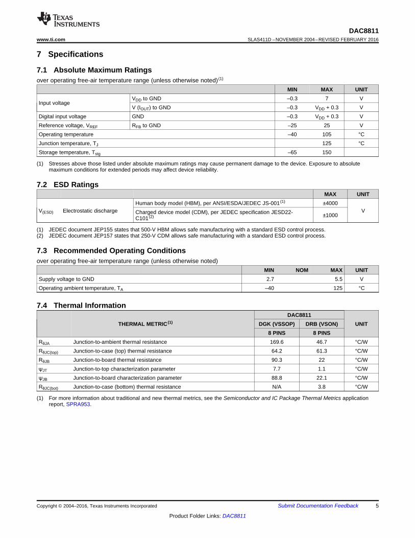
7 Specifications
7.1 Absolute Maximum Ratingsover operating free-air temperature range (unless otherwise noted) (1)
MIN MAX UNIT
Input voltageVDD to GND –0.3 7 VV (IOUT) to GND –0.3 VDD + 0.3 V
Digital input voltage GND –0.3 VDD + 0.3 VReference voltage, VREF RFB to GND –25 25 VOperating temperature –40 105 °CJunction temperature, TJ 125 °CStorage temperature, Tstg –65 150
(1) JEDEC document JEP155 states that 500-V HBM allows safe manufacturing with a standard ESD control process.(2) JEDEC document JEP157 states that 250-V CDM allows safe manufacturing with a standard ESD control process.
7.2 ESD RatingsMAX UNIT
V(ESD) Electrostatic dischargeHuman body model (HBM), per ANSI/ESDA/JEDEC JS-001 (1) ±4000
VCharged device model (CDM), per JEDEC specification JESD22-C101 (2) ±1000
7.3 Recommended Operating Conditionsover operating free-air temperature range (unless otherwise noted)
MIN NOM MAX UNITSupply voltage to GND 2.7 5.5 VOperating ambient temperature, TA –40 125 °C
(1) For more information about traditional and new thermal metrics, see the Semiconductor and IC Package Thermal Metrics applicationreport, SPRA953.
7.4 Thermal Information
THERMAL METRIC (1)DAC8811
UNITDGK (VSSOP) DRB (VSON)8 PINS 8 PINS
RθJA Junction-to-ambient thermal resistance 169.6 46.7 °C/WRθJC(top) Junction-to-case (top) thermal resistance 64.2 61.3 °C/WRθJB Junction-to-board thermal resistance 90.3 22 °C/WψJT Junction-to-top characterization parameter 7.7 1.1 °C/WψJB Junction-to-board characterization parameter 88.8 22.1 °C/WRθJC(bot) Junction-to-case (bottom) thermal resistance N/A 3.8 °C/W

6
DAC8811SLAS411D –NOVEMBER 2004–REVISED FEBRUARY 2016 www.ti.com
Product Folder Links: DAC8811
Submit Documentation Feedback Copyright © 2004–2016, Texas Instruments Incorporated
(1) Specified by design and characterization; not production tested.(2) All ac characteristic tests are performed in a closed-loop system using the THS4011 I-to-V converter amplifier.
7.5 Electrical CharacteristicsVDD = 2.7 V to 5.5 V; IOUT = Virtual GND, GND = 0 V; VREF = 10 V; TA = full operating temperature. All specifications -40°C to85°C, unless otherwise noted.
PARAMETER TEST CONDITIONS MIN TYP MAX UNITSTATIC PERFORMANCE
Resolution 16 BitsRelative accuracy DAC8811C ±1 LSBRelative accuracy DAC8811B ±2 LSBDifferential nonlinearity ±0.5 ±1 LSBOutput leakage current Data = 0000h, TA = 25°C 10 nAOutput leakage current Data = 0000h, TA = TMAX 10 nAFull-scale gain error All ones loaded to DAC register ±1 ±4 mVFull-scale tempco ±3 ppm/°C
OUTPUT CHARACTERISTICS (1)
Output current 2 mAOutput capacitance Code dependent 50 pF
REFERENCE INPUT (1)
VREF Range –15 15 VInput resistance 5 kΩInput capacitance 5 pF
LOGIC INPUTS AND OUTPUT (1)
VIL Input low voltageVDD = 2.7V 0.6 VVDD = 5V 0.8 V
VIH Input high voltageVDD = 2.7V 2.1 VVDD = 5V 2.4 V
IIL Input leakage current 10 µACIL Input capacitance 10 pFPOWER REQUIREMENTSVDD 2.7 5.5 V
IDD (normal operation) Logic inputs = 0 V 5 µAVDD = 4.5 V to 5.5 V VIH = VDD and VIL = GND 3 5 µAVDD = 2.7 V to 3.6 V VIH = VDD and VIL = GND 1 2.5 µA
AC CHARACTERISTICS (1) (2)
BW –3 dB Reference mutiplying BW VREF = 5 VPP, Data = FFFFh 10 MHzDAC glitch impulse VREF = 0 V to 10 V, Data = 7FFFh to 8000h to 7FFFh 2 nV/sFeed through error VOUT/VREF Data = 0000h, VREF = 100 mVRMS, f = 100kHz –70 dBDigital feed through CS = 1 and fCLK = 1 MHz 2 nV/sTotal harmonic distortion VREF = 5 VPP, Data = FFFFh, f = 1 kHz –105 dBOutput spot noise voltage f = 1 kHz, BW = 1 Hz 12 nV/√Hz

CLK 1 16
CS
SDI DB13
tDH
tCL
tCH
tCSH
tDS
tCSS
DB1 DB0DB15 DB14
7
DAC8811www.ti.com SLAS411D –NOVEMBER 2004–REVISED FEBRUARY 2016
Product Folder Links: DAC8811
Submit Documentation FeedbackCopyright © 2004–2016, Texas Instruments Incorporated
(1) Specified by design and characterization; not production tested.(2) All ac characteristic tests are performed in a closed-loop system using the THS4011 I-to-V converter amplifier.
7.6 Timing RequirementsMIN NOM MAX UNIT
INTERFACE TIMINGfCLK Clock input frequency 50 MHzt(CH) Clock pulse width high 10 nst(CL) Clock pulse width low 10 nst(CSS) CS to Clock setup time 0 nst(CSH) Clock to CS hold time 10 nst(DS) Data setup time 5 nst(DH) Data hold time 10 nsAC CHARACTERISTICS (1) (2)
ts Output voltage settling time
To ±0.1% of full-scale, Data = 0000h toFFFFh to 0000h 0.3 µs
To ±0.0015% of full-scale, Data = 0000hto FFFFh to 0000h 0.5 µs
Figure 1. DAC8811 Timing Diagram

1.0
0.8
0.6
0.4
0.2
0
- 0.2
- 0.4
- 0.6
- 0.8
- 1.0
INL
(LS
B)
0 8192 16384 24576 32768 40960 49512 57344 65536
Digital Input Code
1.0
0.8
0.6
0.4
0.2
0
- 0.2
- 0.4
- 0.6
- 0.8
- 1.0
DN
L(L
SB
)
0 8192 16384 24576 32768 40960 49512 57344 65536
Digital Input Code
1.0
0.8
0.6
0.4
0.2
0
- 0.2
- 0.4
- 0.6
- 0.8
- 1.0
INL
(LS
B)
0 8192 16384 24576 32768 40960 49512 57344 65536
Digital Input Code
1.0
0.8
0.6
0.4
0.2
0
- 0.2
- 0.4
- 0.6
- 0.8
- 1.0
DN
L(L
SB
)
0 8192 16384 24576 32768 40960 49512 57344 65536
Digital Input Code
1.0
0.8
0.6
0.4
0.2
0
- 0.2
- 0.4
- 0.6
- 0.8
- 1.0
0 8192 16384 24576 32768 40960 49512 57344 65536
INL
(LS
B)
Digital Input Code
1.0
0.8
0.6
0.4
0.2
0
- 0.2
- 0.4
- 0.6
- 0.8
- 1.0
DN
L(L
SB
)
0 8192 16384 24576 32768 40960 49512 57344 65536
Digital Input Code
8
DAC8811SLAS411D –NOVEMBER 2004–REVISED FEBRUARY 2016 www.ti.com
Product Folder Links: DAC8811
Submit Documentation Feedback Copyright © 2004–2016, Texas Instruments Incorporated
7.7 Typical Characteristics: VDD = 5 VAt TA = 25°C, +VDD = 5 V, unless otherwise noted.
TA = 25°C
Figure 2. Linearity Error vs Digital Input Code
TA = 25°C
Figure 3. Differential Linearity Error vs Digital Input Code
TA = –40°C
Figure 4. Linearity Error vs Digital Input Code
TA = –40°C
Figure 5. Differential Linearity Error vs Digital Input Code
TA = 85°C
Figure 6. Linearity Error vs Digital Input Code
TA = 85°C
Figure 7. Differential Linearity Error vs Digital Input Code

Time (0.2 Ps/div)
Trigger Pulse
Code: 7FFFh to 8000h
Out
put V
olta
ge (
50 m
V/d
iv)
Time (0.1 Ps/div)
Trigger Pulse
Voltage Output Setting
Out
put V
olta
ge (
5 V
/div
)
60
−6−12−18−24−30−36−42−48−54−60−66−72−78−84−90−96
−102−108−114
10 100 1k 10k 100k 1M 10M 100M
A
Dig
ital C
od
e
tte
nu
ati
on
(dB
)
Bandwidth (Hz)
0x00010x00020x00040x00080x00100x00200x00400x00800x01000x02000x04000x08000x10000x20000x4000
0x80000xFFFF
0x0000
9
DAC8811www.ti.com SLAS411D –NOVEMBER 2004–REVISED FEBRUARY 2016
Product Folder Links: DAC8811
Submit Documentation FeedbackCopyright © 2004–2016, Texas Instruments Incorporated
Typical Characteristics: VDD = 5 V (continued)At TA = 25°C, +VDD = 5 V, unless otherwise noted.
Figure 8. Supply Current vs Logic Input Voltage Figure 9. Reference Multiplying Bandwidth
Figure 10. DAC Glitch Figure 11. DAC Settling Time

1.0
0.8
0.6
0.4
0.2
0
- 0.2
- 0.4
- 0.6
- 0.8
- 1.0
INL
(LS
B)
0 8192 16384 24576 32768 40960 49512 57344 65536
Digital Input Code
1.0
0.8
0.6
0.4
0.2
0
- 0.2
- 0.4
- 0.6
- 0.8
- 1.0
DN
L(L
SB
)
0 8192 16384 24576 32768 40960 49512 57344 65536
Digital Input Code
1.0
0.8
0.6
0.4
0.2
0
- 0.2
- 0.4
- 0.6
- 0.8
- 1.0
INL
(LS
B)
0 8192 16384 24576 32768 40960 49512 57344 65536
Digital Input Code
1.0
0.8
0.6
0.4
0.2
0
- 0.2
- 0.4
- 0.6
- 0.8
- 1.0
DN
L(L
SB
)
0 8192 16384 24576 32768 40960 49512 57344 65536
Digital Input Code
1.0
0.8
0.6
0.4
0.2
0
- 0.2
- 0.4
- 0.6
- 0.8
- 1.0
INL
(LS
B)
0 8192 16384 24576 32768 40960 49512 57344 65536
Digital Input Code
1.0
0.8
0.6
0.4
0.2
0
- 0.2
- 0.4
- 0.6
- 0.8
- 1.0
DN
L(L
SB
)
0 8192 16384 24576 32768 40960 49512 57344 65536
Digital Input Code
10
DAC8811SLAS411D –NOVEMBER 2004–REVISED FEBRUARY 2016 www.ti.com
Product Folder Links: DAC8811
Submit Documentation Feedback Copyright © 2004–2016, Texas Instruments Incorporated
7.8 Typical Characteristics: VDD = 2.7 VAt TA = 25°C, +VDD = 2.7 V, unless otherwise noted.
TA = 25°C
Figure 12. Linearity Error vs Digital Input Code
TA = 25°C
Figure 13. Differential Linearity Error vs Digital Input Code
TA = –40°C
Figure 14. Linearity Error vs Digital Input Code
TA = –40°C
Figure 15. Differential Linearity Error vs Digital Input Code
TA = 85°C
Figure 16. Linearity Error vs Digital Input Code
TA = 85°C
Figure 17. Differential Linearity Error vs Digital Input Code

OUT REFCODE
V V x65536
D/A
Converter
Power-OnReset
DAC
Register
Shift
Register
16
16
RFB
IOUT
GND
VDD
VREF
CS
CLK
SDI
DAC8811
11
DAC8811www.ti.com SLAS411D –NOVEMBER 2004–REVISED FEBRUARY 2016
Product Folder Links: DAC8811
Submit Documentation FeedbackCopyright © 2004–2016, Texas Instruments Incorporated
8 Detailed Description
8.1 OverviewThe DAC8811 is a single channel current output, 16-bit digital-to-analog converter (DAC). The device includes a3-wire serial interface to communicate with most DSPs.
8.2 Functional Block Diagram
8.3 Feature DescriptionThe DAC8811 is a single channel current output, 16-bit digital-to-analog converter (DAC). The architecture,illustrated in Figure 18, is an R-2R ladder configuration with the three MSBs segmented. Each 2R leg of theladder is either switched to GND or the IOUT terminal. The IOUT terminal of the DAC is held at a virtual GNDpotential by the use of an external I/V converter op amp. The R-2R ladder is connected to an external referenceinput VREF that determines the DAC full-scale current. The R-2R ladder presents a code independent loadimpedance to the external reference of 5 kΩ ±25%. The external reference voltage can vary in a range of -15 Vto 15 V, thus providing bipolar IOUT current operation. By using an external I/V converter and the DAC8811 RFBresistor, output voltage ranges of -VREF to VREF can be generated.
Figure 18. Equivalent R-2R DAC Circuit
When using an external I/V converter and the DAC8811 RFB resistor, the DAC output voltage is given byEquation 1:
(1)

12
DAC8811SLAS411D –NOVEMBER 2004–REVISED FEBRUARY 2016 www.ti.com
Product Folder Links: DAC8811
Submit Documentation Feedback Copyright © 2004–2016, Texas Instruments Incorporated
Feature Description (continued)Each DAC code determines the 2R leg switch position to either GND or IOUT. Because the DAC outputimpedance as seen looking into the IOUT terminal changes versus code, the external I/V converter noise gain willalso change. Because of this, the external I/V converter op amp must have a sufficiently low offset voltage suchthat the amplifier offset is not modulated by the DAC IOUT terminal impedance change. External op amps withlarge offset voltages can produce INL errors in the transfer function of the DAC8811 due to offset modulationversus DAC code. For best linearity performance of the DAC8811, an operational amplifier (OPA277) isrecommended (Figure 19). This circuit allows VREF swinging from -10 V to +10 V.
Figure 19. Voltage Output Configuration
8.3.1 Stability CircuitFor a current-to-voltage design (see Figure 20), the DAC8811 current output (IOUT) and the connection with theinverting node of the op amp should be as short as possible and according to correct PCB layout design. Foreach code change, there is a step function. If the GBP of the op amp is limited and parasitic capacitance isexcessive at the inverting node then gain peaking is possible. Therefore, for circuit stability, a compensationcapacitor C1 (4 pF to 20 pF typ) can be added to the design, as shown in Figure 20.
Figure 20. Gain Peaking Prevention Circuit With Compensation Capacitor
8.3.2 Positive Voltage Output CircuitAs Figure 21 illustrates, in order to generate a positive voltage output, a negative reference is input to theDAC8811. This design is suggested instead of using an inverting amp to invert the output due to tolerance errorsof the resistor. For a negative reference, VOUT and GND of the reference are level-shifted to a virtual ground anda –2.5 V input to the DAC8811 with an op amp.

L REF
R2 R3 / R1I x V x D
R3
-2.5V VOUT +2.5V(-10sGsOUT G+10V)
10 k: 10 k:
5 k:
OUT REFD
V -1 x V32,768
§ · ¨ ¸© ¹
0 VOUT +2.5V
13
DAC8811www.ti.com SLAS411D –NOVEMBER 2004–REVISED FEBRUARY 2016
Product Folder Links: DAC8811
Submit Documentation FeedbackCopyright © 2004–2016, Texas Instruments Incorporated
Feature Description (continued)
Figure 21. Positive Voltage Output Circuit
8.3.3 Bipolar Output CircuitThe DAC8811, as a 2-quadrant multiplying DAC, can be used to generate a unipolar output. The polarity of thefull-scale output IOUT is the inverse of the input reference voltage at VREF.
Some applications require full 4-quadrant multiplying capabilities or bipolar output swing. As shown in Figure 22,external op amp U4 is added as a summing amp and has a gain of 2X that widens the output span to 5 V. A 4-quadrant multiplying circuit is implemented by using a 2.5-V offset of the reference voltage to bias U4. Accordingto the circuit transfer equation given in Equation 2, input data (D) from code 0 to full scale produces outputvoltages of VOUT = -2.5 V to VOUT = +2.5 V.
(2)
External resistance mismatching is the significant error in Figure 22.
Figure 22. Bipolar Output Circuit
8.3.4 Programmable Current Source CircuitA DAC8811 can be integrated into the circuit in Figure 23 to implement an improved Howland current pump forprecise voltage to current conversions. Bidirectional current flow and high voltage compliance are two features ofthe circuit. With a matched resistor network, the load current of the circuit is shown by Equation 3:
(3)
The value of R3 in the previous equation can be reduced to increase the output current drive of U3. U3 can drive±20 mA in both directions with voltage compliance limited up to 15 V by the U3 voltage supply. Elimination of thecircuit compensation capacitor C1 in the circuit is not suggested as a result of the change in the outputimpedance ZO, according to Equation 4:

VDD
VDD
VREFVREF
DAC8811
U1
RFB
OPA277U2
IOUT
GND
150 kW
R1’
15 kW
R2’
C1 10 pF
OPA277U2
15 kW
R2
50 W
R3’
50 W
R3
VOUT
150 kW
R1 IL
LOAD
−
+
+
−
O
R1'R3 R1 R2Z
R1(R2' R3') R1'(R2 R3)
14
DAC8811SLAS411D –NOVEMBER 2004–REVISED FEBRUARY 2016 www.ti.com
Product Folder Links: DAC8811
Submit Documentation Feedback Copyright © 2004–2016, Texas Instruments Incorporated
Feature Description (continued)
(1) ↑+ Positive logic transition; X = Don't care
(4)
As shown in Equation 4, with matched resistors, ZO is infinite and the circuit is optimum for use as a currentsource. However, if unmatched resistors are used, ZO is positive or negative with negative output impedancebeing a potential cause of oscillation. Therefore, by incorporating C1 into the circuit, possible oscillation problemsare eliminated. The value of C1 can be determined for critical applications; for most applications, however, avalue of several pF is suggested.
Figure 23. Programmable Bidirectional Current Source Circuit
8.4 Device Functional Mode
Table 1. Control Logic Truth Table (1)
CLK CS SERIAL SHIFT REGISTER DAC REGISTERX H No effect Latched↑+ L Shift register data advanced one bit LatchedX H No effect LatchedX ↑+ Shift register data transferred to DAC register New data loaded from serial register

Invalid Write Sequence:CS HIGH before 16th Rising Edge
Valid Write Sequence:Output Updates on 16th Rising Edge
CLK
CS
DIN DB15 DB0 DB15 DB0
15
DAC8811www.ti.com SLAS411D –NOVEMBER 2004–REVISED FEBRUARY 2016
Product Folder Links: DAC8811
Submit Documentation FeedbackCopyright © 2004–2016, Texas Instruments Incorporated
8.5 Programming
8.5.1 DAC8811 Input Shift RegisterThe DAC8811 has a 3-wire serial interface (CS, SCLK, and DIN) compatible with SPI, QSPI, and Microwireinterface standards, as well as most DSPs. See Figure 1 for an example of a typical write sequence.
The input shift register is 16 bits wide, as shown in Figure 25. The write sequence begins by bringing the CS linelow. Data from the DIN line are clocked into the 16-bit shift register on each rising edge of CLK. The serial clockfrequency can be as high as 50 MHz, making the DAC8811 compatible with high-speed DSPs. On the 16th risingedge of the serial clock, the last data bit is clocked in and the programmed function is executed.
At this point, the CS line may be kept low or brought high. In either case, it must be brought high for a minimumof 20 ns before the next write sequence so that a falling edge of CS can initiate the next write sequence.
Figure 24. Data Input Register
DB15 DB0D15 D15 D13 D12 D11 D10 D9 D8 D7 D6 D5 D4 D3 D2 D1 D0
LEGEND: R/W = Read/Write; R = Read only; -n = value after reset
Figure 25. CS Interrupt Facility

FB2 REF FB2
OUT REFbitsG1 G2
2 V x Code RV Code x x V
R R2
§ · § · ¨ ¸ ¨ ¸© ¹ © ¹
++
VOUT
RFB2RG2
RG1
A2
A1MDAC
VREF
IOUT
VDAC
RFBREFIN
Trans-Impedance Stage Gain and Offset Stage
16
DAC8811SLAS411D –NOVEMBER 2004–REVISED FEBRUARY 2016 www.ti.com
Product Folder Links: DAC8811
Submit Documentation Feedback Copyright © 2004–2016, Texas Instruments Incorporated
9 Application and Implementation
NOTEInformation in the following applications sections is not part of the TI componentspecification, and TI does not warrant its accuracy or completeness. TI’s customers areresponsible for determining suitability of components for their purposes. Customers shouldvalidate and test their design implementation to confirm system functionality.
9.1 Application InformationThis design features the DAC8811 followed by a four-quadrant circuit for multiplying DACs. The circuit conditionsthe current output of an MDAC into a symmetrical bipolar voltage. The design uses an operational amplifier in atransimpedance configuration to convert the MDAC current into a voltage followed by an additional amplifier in asumming configuration to apply an offset voltage.
9.2 Typical Application
Figure 26. Typical Application
9.2.1 Design RequirementsUsing a multiplying DAC requires a transimpedance stage with an amplifier with minimal input offset voltage. Thetolerance of the external resistors will vary depending on the goals of the application, but for optimal performancewith the DAC8811 the tolerance should be 0.1 % for all of the external resistors. The summing stage amplifieralso needs low input-offset voltage and enough slew rate for the output range desired.
9.2.2 Detailed Design ProcedureThe first stage of the design converts the current output of the MDAC (IOUT) to a voltage (VOUT) using an amplifierin a transimpedance configuration. A typical MDAC features an on-chip feedback resistor sized appropriately tomatch the ratio of the resistor values used in the DAC R-2R ladder. This resistor is available using the inputshown in Figure 26 called RFB on the MDAC. The MDAC reference and the output of the transimpedance stageare then connected to the inverting input of the amplifier in the summing stage to produce the output that isdefined by Equation 5.
(5)

Input Code (decimal)
Out
put V
olta
ge (
V)
0 8192 16384 24576 32768 40960 49152 57344 65536-10
-5
0
5
10
D001Input Code (decimal)
Out
put E
rror
(%
FS
R)
0 8192 16384 24576 32768 40960 49152 57344 655360
0.002
0.004
0.006
0.008
0.01
0.012
0.014
D002
17
DAC8811www.ti.com SLAS411D –NOVEMBER 2004–REVISED FEBRUARY 2016
Product Folder Links: DAC8811
Submit Documentation FeedbackCopyright © 2004–2016, Texas Instruments Incorporated
Typical Application (continued)9.2.3 Application CurvesFigure 27 shows the output voltage vs code of this design, while Figure 28 shows the output error vs code. Keepin mind that the error gets worse as the output code increases because the contribution of the gain errorincreases with code.
Figure 27. Output Voltage vs Input Code Figure 28. Output Current vs Input Code
10 Power Supply Recommendations
These devices can operate within the specified supply voltage range of 2.7 V to 5.5 V. The power applied toAVDD should be well-regulated and low-noise. In order to further minimize noise from the power supplies, astrong recommendation is to include a pair of 100 pF and 1 nF capacitors and a 0.1 μF to 1 μF bypass capacitor.The current consumption of the AVDD pin, the short-circuit current limit, and the load current for these devicesare listed in the Electrical Characteristics table. Choose the power supplies for these devices to meet theaforementioned current requirements.

18
DAC8811SLAS411D –NOVEMBER 2004–REVISED FEBRUARY 2016 www.ti.com
Product Folder Links: DAC8811
Submit Documentation Feedback Copyright © 2004–2016, Texas Instruments Incorporated
11 Layout
11.1 Layout GuidelinesA precision analog component requires careful layout, adequate bypassing, and clean, well-regulated powersupplies. The DAC8811devices offer single-supply operation, and are often used in close proximity with digitallogic, microcontrollers, microprocessors, and digital signal processors. The more digital logic present in thedesign and the higher the switching speed, the more difficult it is to keep digital noise from appearing at theoutput. As a result of the single ground pin of the DAC8811, all return currents (including digital and analogreturn currents for the DAC) must flow through a single point. Ideally, GND would be connected directly to ananalog ground plane. This plane would be separate from the ground connection for the digital components untilthey were connected at the power-entry point of the system. The power applied to AVDD should be well-regulated and low noise. Switching power supplies and dc-dc converters often have high-frequency glitches orspikes riding on the output voltage. In addition, digital components can create similar high-frequency spikes astheir internal logic switches states. This noise can easily couple into the DAC output voltage through variouspaths between the power connections and analog output. As with the GND connection, AVDD should beconnected to a power-supply plane or trace that is separate from the connection for digital logic until they areconnected at the power-entry point. In addition, a pair of 100-pF to 1-nF capacitors and a 0.1-μF to 1-μF bypasscapacitor are strongly recommended. In some situations, additional bypassing may be required, such as a 100μF electrolytic capacitor or even a pi filter made up of inductors and capacitors – all designed essentially toprovide low-pass filtering for the supply and remove the high-frequency noise.
While all the other recommendations apply to most DACs, multiplying DACs also require that the transimpedanceamplifier be placed in close proximity in order to minimize non-linearity errors introduced by any resistancebetween the IOUT pin and V- pin of the amplifier.
11.2 Layout Example
Figure 29. DAC8811 Layout Example

19
DAC8811www.ti.com SLAS411D –NOVEMBER 2004–REVISED FEBRUARY 2016
Product Folder Links: DAC8811
Submit Documentation FeedbackCopyright © 2004–2016, Texas Instruments Incorporated
12 Device and Documentation Support
12.1 Documentation Support
12.1.1 Related DocumentationFor related documentation see the following:• DAC8801/11EVM, SLAU151• Interfacing the DAC8811 to the MSP430F449, SLAA238• Topology and Noise Using Multiplying DAC, SBAA146
12.2 Community ResourcesThe following links connect to TI community resources. Linked contents are provided "AS IS" by the respectivecontributors. They do not constitute TI specifications and do not necessarily reflect TI's views; see TI's Terms ofUse.
TI E2E™ Online Community TI's Engineer-to-Engineer (E2E) Community. Created to foster collaborationamong engineers. At e2e.ti.com, you can ask questions, share knowledge, explore ideas and helpsolve problems with fellow engineers.
Design Support TI's Design Support Quickly find helpful E2E forums along with design support tools andcontact information for technical support.
12.3 TrademarksE2E is a trademark of Texas Instruments.All other trademarks are the property of their respective owners.
12.4 Electrostatic Discharge CautionThese devices have limited built-in ESD protection. The leads should be shorted together or the device placed in conductive foamduring storage or handling to prevent electrostatic damage to the MOS gates.
12.5 GlossarySLYZ022 — TI Glossary.
This glossary lists and explains terms, acronyms, and definitions.
13 Mechanical, Packaging, and Orderable InformationThe following pages include mechanical, packaging, and orderable information. This information is the mostcurrent data available for the designated devices. This data is subject to change without notice and revision ofthis document. For browser-based versions of this data sheet, refer to the left-hand navigation.

PACKAGE OPTION ADDENDUM
www.ti.com 4-Feb-2016
Addendum-Page 1
PACKAGING INFORMATION
Orderable Device Status(1)
Package Type PackageDrawing
Pins PackageQty
Eco Plan(2)
Lead/Ball Finish(6)
MSL Peak Temp(3)
Op Temp (°C) Device Marking(4/5)
Samples
DAC8811IBDGKR ACTIVE VSSOP DGK 8 2500 Green (RoHS& no Sb/Br)
CU NIPDAUAG Level-2-260C-1 YEAR -40 to 85 D11
DAC8811IBDGKT ACTIVE VSSOP DGK 8 250 Green (RoHS& no Sb/Br)
CU NIPDAUAG Level-2-260C-1 YEAR -40 to 85 D11
DAC8811IBDGKTG4 ACTIVE VSSOP DGK 8 250 Green (RoHS& no Sb/Br)
CU NIPDAUAG Level-2-260C-1 YEAR -40 to 85 D11
DAC8811IBDRBT ACTIVE SON DRB 8 250 Green (RoHS& no Sb/Br)
CU NIPDAU Level-2-260C-1 YEAR -40 to 85 D11
DAC8811IBDRBTG4 ACTIVE SON DRB 8 250 Green (RoHS& no Sb/Br)
CU NIPDAU Level-2-260C-1 YEAR -40 to 85 D11
DAC8811ICDGKR ACTIVE VSSOP DGK 8 2500 Green (RoHS& no Sb/Br)
CU NIPDAUAG Level-2-260C-1 YEAR -40 to 85 D11
DAC8811ICDGKRG4 ACTIVE VSSOP DGK 8 2500 Green (RoHS& no Sb/Br)
CU NIPDAUAG Level-2-260C-1 YEAR -40 to 85 D11
DAC8811ICDGKT ACTIVE VSSOP DGK 8 250 Green (RoHS& no Sb/Br)
CU NIPDAUAG Level-2-260C-1 YEAR -40 to 85 D11
DAC8811ICDGKTG4 ACTIVE VSSOP DGK 8 250 Green (RoHS& no Sb/Br)
CU NIPDAUAG Level-2-260C-1 YEAR -40 to 85 D11
DAC8811ICDRBT ACTIVE SON DRB 8 250 Green (RoHS& no Sb/Br)
CU NIPDAU Level-2-260C-1 YEAR -40 to 85 D11
DAC8811ICDRBTG4 ACTIVE SON DRB 8 250 Green (RoHS& no Sb/Br)
CU NIPDAU Level-2-260C-1 YEAR -40 to 85 D11
(1) The marketing status values are defined as follows:ACTIVE: Product device recommended for new designs.LIFEBUY: TI has announced that the device will be discontinued, and a lifetime-buy period is in effect.NRND: Not recommended for new designs. Device is in production to support existing customers, but TI does not recommend using this part in a new design.PREVIEW: Device has been announced but is not in production. Samples may or may not be available.OBSOLETE: TI has discontinued the production of the device.
(2) Eco Plan - The planned eco-friendly classification: Pb-Free (RoHS), Pb-Free (RoHS Exempt), or Green (RoHS & no Sb/Br) - please check http://www.ti.com/productcontent for the latest availabilityinformation and additional product content details.TBD: The Pb-Free/Green conversion plan has not been defined.Pb-Free (RoHS): TI's terms "Lead-Free" or "Pb-Free" mean semiconductor products that are compatible with the current RoHS requirements for all 6 substances, including the requirement thatlead not exceed 0.1% by weight in homogeneous materials. Where designed to be soldered at high temperatures, TI Pb-Free products are suitable for use in specified lead-free processes.

PACKAGE OPTION ADDENDUM
www.ti.com 4-Feb-2016
Addendum-Page 2
Pb-Free (RoHS Exempt): This component has a RoHS exemption for either 1) lead-based flip-chip solder bumps used between the die and package, or 2) lead-based die adhesive used betweenthe die and leadframe. The component is otherwise considered Pb-Free (RoHS compatible) as defined above.Green (RoHS & no Sb/Br): TI defines "Green" to mean Pb-Free (RoHS compatible), and free of Bromine (Br) and Antimony (Sb) based flame retardants (Br or Sb do not exceed 0.1% by weightin homogeneous material)
(3) MSL, Peak Temp. - The Moisture Sensitivity Level rating according to the JEDEC industry standard classifications, and peak solder temperature.
(4) There may be additional marking, which relates to the logo, the lot trace code information, or the environmental category on the device.
(5) Multiple Device Markings will be inside parentheses. Only one Device Marking contained in parentheses and separated by a "~" will appear on a device. If a line is indented then it is a continuationof the previous line and the two combined represent the entire Device Marking for that device.
(6) Lead/Ball Finish - Orderable Devices may have multiple material finish options. Finish options are separated by a vertical ruled line. Lead/Ball Finish values may wrap to two lines if the finishvalue exceeds the maximum column width.
Important Information and Disclaimer:The information provided on this page represents TI's knowledge and belief as of the date that it is provided. TI bases its knowledge and belief on informationprovided by third parties, and makes no representation or warranty as to the accuracy of such information. Efforts are underway to better integrate information from third parties. TI has taken andcontinues to take reasonable steps to provide representative and accurate information but may not have conducted destructive testing or chemical analysis on incoming materials and chemicals.TI and TI suppliers consider certain information to be proprietary, and thus CAS numbers and other limited information may not be available for release.
In no event shall TI's liability arising out of such information exceed the total purchase price of the TI part(s) at issue in this document sold by TI to Customer on an annual basis.

TAPE AND REEL INFORMATION
*All dimensions are nominal
Device PackageType
PackageDrawing
Pins SPQ ReelDiameter
(mm)
ReelWidth
W1 (mm)
A0(mm)
B0(mm)
K0(mm)
P1(mm)
W(mm)
Pin1Quadrant
DAC8811IBDGKR VSSOP DGK 8 2500 330.0 12.4 5.3 3.4 1.4 8.0 12.0 Q1
DAC8811IBDGKT VSSOP DGK 8 250 330.0 12.4 5.3 3.4 1.4 8.0 12.0 Q1
DAC8811IBDRBT SON DRB 8 250 180.0 12.4 3.3 3.3 1.1 8.0 12.0 Q2
DAC8811ICDGKR VSSOP DGK 8 2500 330.0 12.4 5.3 3.4 1.4 8.0 12.0 Q1
DAC8811ICDGKT VSSOP DGK 8 250 330.0 12.4 5.3 3.4 1.4 8.0 12.0 Q1
DAC8811ICDRBT SON DRB 8 250 180.0 12.4 3.3 3.3 1.1 8.0 12.0 Q2
PACKAGE MATERIALS INFORMATION
www.ti.com 30-Apr-2018
Pack Materials-Page 1

*All dimensions are nominal
Device Package Type Package Drawing Pins SPQ Length (mm) Width (mm) Height (mm)
DAC8811IBDGKR VSSOP DGK 8 2500 366.0 364.0 50.0
DAC8811IBDGKT VSSOP DGK 8 250 366.0 364.0 50.0
DAC8811IBDRBT SON DRB 8 250 210.0 185.0 35.0
DAC8811ICDGKR VSSOP DGK 8 2500 366.0 364.0 50.0
DAC8811ICDGKT VSSOP DGK 8 250 366.0 364.0 50.0
DAC8811ICDRBT SON DRB 8 250 210.0 185.0 35.0
PACKAGE MATERIALS INFORMATION
www.ti.com 30-Apr-2018
Pack Materials-Page 2


www.ti.com
PACKAGE OUTLINE
C
8X 0.370.25
1.75 0.12X
1.95
1.5 0.1
6X 0.65
1 MAX
8X 0.50.3
0.050.00
(0.65)
A 3.12.9
B
3.12.9
(DIM A) TYP4X (0.23)
VSON - 1 mm max heightDRB0008APLASTIC SMALL OUTLINE - NO LEAD
4218875/A 01/2018
DIM AOPT 1 OPT 2(0.1) (0.2)
PIN 1 INDEX AREA
SEATING PLANE
0.08 C
1
4 5
8
(OPTIONAL)PIN 1 ID 0.1 C A B
0.05 C
THERMAL PADEXPOSED
NOTES: 1. All linear dimensions are in millimeters. Any dimensions in parenthesis are for reference only. Dimensioning and tolerancing per ASME Y14.5M. 2. This drawing is subject to change without notice. 3. The package thermal pad must be soldered to the printed circuit board for thermal and mechanical performance.
SCALE 4.000

www.ti.com
EXAMPLE BOARD LAYOUT
0.07 MINALL AROUND
0.07 MAXALL AROUND
8X (0.31)
(1.75)
(2.8)
6X (0.65)
(1.5)
( 0.2) VIATYP
(0.5)
(0.625)
8X (0.6)
(R0.05) TYP
(0.825)
(0.23)
(0.65)
VSON - 1 mm max heightDRB0008APLASTIC SMALL OUTLINE - NO LEAD
4218875/A 01/2018
SYMM
1
45
8
LAND PATTERN EXAMPLEEXPOSED METAL SHOWN
SCALE:20X
NOTES: (continued) 4. This package is designed to be soldered to a thermal pad on the board. For more information, see Texas Instruments literature number SLUA271 (www.ti.com/lit/slua271).5. Vias are optional depending on application, refer to device data sheet. If any vias are implemented, refer to their locations shown on this view. It is recommended that vias under paste be filled, plugged or tented.
SYMM
SOLDER MASKOPENINGSOLDER MASK
METAL UNDER
SOLDER MASKDEFINED
EXPOSEDMETAL
METALSOLDER MASKOPENING
SOLDER MASK DETAILS
NON SOLDER MASKDEFINED
(PREFERRED)
EXPOSEDMETAL

www.ti.com
EXAMPLE STENCIL DESIGN
(R0.05) TYP
8X (0.31)
8X (0.6)
(1.34)
(1.55)
(2.8)
6X (0.65)
4X(0.725)
4X (0.23)
(2.674)
(0.65)
VSON - 1 mm max heightDRB0008APLASTIC SMALL OUTLINE - NO LEAD
4218875/A 01/2018
NOTES: (continued) 6. Laser cutting apertures with trapezoidal walls and rounded corners may offer better paste release. IPC-7525 may have alternate design recommendations.
SOLDER PASTE EXAMPLEBASED ON 0.125 mm THICK STENCIL
EXPOSED PAD
84% PRINTED SOLDER COVERAGE BY AREASCALE:25X
SYMM
1
45
8
METALTYP
SYMM


IMPORTANT NOTICE
Texas Instruments Incorporated (TI) reserves the right to make corrections, enhancements, improvements and other changes to itssemiconductor products and services per JESD46, latest issue, and to discontinue any product or service per JESD48, latest issue. Buyersshould obtain the latest relevant information before placing orders and should verify that such information is current and complete.TI’s published terms of sale for semiconductor products (http://www.ti.com/sc/docs/stdterms.htm) apply to the sale of packaged integratedcircuit products that TI has qualified and released to market. Additional terms may apply to the use or sale of other types of TI products andservices.Reproduction of significant portions of TI information in TI data sheets is permissible only if reproduction is without alteration and isaccompanied by all associated warranties, conditions, limitations, and notices. TI is not responsible or liable for such reproduceddocumentation. Information of third parties may be subject to additional restrictions. Resale of TI products or services with statementsdifferent from or beyond the parameters stated by TI for that product or service voids all express and any implied warranties for theassociated TI product or service and is an unfair and deceptive business practice. TI is not responsible or liable for any such statements.Buyers and others who are developing systems that incorporate TI products (collectively, “Designers”) understand and agree that Designersremain responsible for using their independent analysis, evaluation and judgment in designing their applications and that Designers havefull and exclusive responsibility to assure the safety of Designers' applications and compliance of their applications (and of all TI productsused in or for Designers’ applications) with all applicable regulations, laws and other applicable requirements. Designer represents that, withrespect to their applications, Designer has all the necessary expertise to create and implement safeguards that (1) anticipate dangerousconsequences of failures, (2) monitor failures and their consequences, and (3) lessen the likelihood of failures that might cause harm andtake appropriate actions. Designer agrees that prior to using or distributing any applications that include TI products, Designer willthoroughly test such applications and the functionality of such TI products as used in such applications.TI’s provision of technical, application or other design advice, quality characterization, reliability data or other services or information,including, but not limited to, reference designs and materials relating to evaluation modules, (collectively, “TI Resources”) are intended toassist designers who are developing applications that incorporate TI products; by downloading, accessing or using TI Resources in anyway, Designer (individually or, if Designer is acting on behalf of a company, Designer’s company) agrees to use any particular TI Resourcesolely for this purpose and subject to the terms of this Notice.TI’s provision of TI Resources does not expand or otherwise alter TI’s applicable published warranties or warranty disclaimers for TIproducts, and no additional obligations or liabilities arise from TI providing such TI Resources. TI reserves the right to make corrections,enhancements, improvements and other changes to its TI Resources. TI has not conducted any testing other than that specificallydescribed in the published documentation for a particular TI Resource.Designer is authorized to use, copy and modify any individual TI Resource only in connection with the development of applications thatinclude the TI product(s) identified in such TI Resource. NO OTHER LICENSE, EXPRESS OR IMPLIED, BY ESTOPPEL OR OTHERWISETO ANY OTHER TI INTELLECTUAL PROPERTY RIGHT, AND NO LICENSE TO ANY TECHNOLOGY OR INTELLECTUAL PROPERTYRIGHT OF TI OR ANY THIRD PARTY IS GRANTED HEREIN, including but not limited to any patent right, copyright, mask work right, orother intellectual property right relating to any combination, machine, or process in which TI products or services are used. Informationregarding or referencing third-party products or services does not constitute a license to use such products or services, or a warranty orendorsement thereof. Use of TI Resources may require a license from a third party under the patents or other intellectual property of thethird party, or a license from TI under the patents or other intellectual property of TI.TI RESOURCES ARE PROVIDED “AS IS” AND WITH ALL FAULTS. TI DISCLAIMS ALL OTHER WARRANTIES ORREPRESENTATIONS, EXPRESS OR IMPLIED, REGARDING RESOURCES OR USE THEREOF, INCLUDING BUT NOT LIMITED TOACCURACY OR COMPLETENESS, TITLE, ANY EPIDEMIC FAILURE WARRANTY AND ANY IMPLIED WARRANTIES OFMERCHANTABILITY, FITNESS FOR A PARTICULAR PURPOSE, AND NON-INFRINGEMENT OF ANY THIRD PARTY INTELLECTUALPROPERTY RIGHTS. TI SHALL NOT BE LIABLE FOR AND SHALL NOT DEFEND OR INDEMNIFY DESIGNER AGAINST ANY CLAIM,INCLUDING BUT NOT LIMITED TO ANY INFRINGEMENT CLAIM THAT RELATES TO OR IS BASED ON ANY COMBINATION OFPRODUCTS EVEN IF DESCRIBED IN TI RESOURCES OR OTHERWISE. IN NO EVENT SHALL TI BE LIABLE FOR ANY ACTUAL,DIRECT, SPECIAL, COLLATERAL, INDIRECT, PUNITIVE, INCIDENTAL, CONSEQUENTIAL OR EXEMPLARY DAMAGES INCONNECTION WITH OR ARISING OUT OF TI RESOURCES OR USE THEREOF, AND REGARDLESS OF WHETHER TI HAS BEENADVISED OF THE POSSIBILITY OF SUCH DAMAGES.Unless TI has explicitly designated an individual product as meeting the requirements of a particular industry standard (e.g., ISO/TS 16949and ISO 26262), TI is not responsible for any failure to meet such industry standard requirements.Where TI specifically promotes products as facilitating functional safety or as compliant with industry functional safety standards, suchproducts are intended to help enable customers to design and create their own applications that meet applicable functional safety standardsand requirements. Using products in an application does not by itself establish any safety features in the application. Designers mustensure compliance with safety-related requirements and standards applicable to their applications. Designer may not use any TI products inlife-critical medical equipment unless authorized officers of the parties have executed a special contract specifically governing such use.Life-critical medical equipment is medical equipment where failure of such equipment would cause serious bodily injury or death (e.g., lifesupport, pacemakers, defibrillators, heart pumps, neurostimulators, and implantables). Such equipment includes, without limitation, allmedical devices identified by the U.S. Food and Drug Administration as Class III devices and equivalent classifications outside the U.S.TI may expressly designate certain products as completing a particular qualification (e.g., Q100, Military Grade, or Enhanced Product).Designers agree that it has the necessary expertise to select the product with the appropriate qualification designation for their applicationsand that proper product selection is at Designers’ own risk. Designers are solely responsible for compliance with all legal and regulatoryrequirements in connection with such selection.Designer will fully indemnify TI and its representatives against any damages, costs, losses, and/or liabilities arising out of Designer’s non-compliance with the terms and provisions of this Notice.
Mailing Address: Texas Instruments, Post Office Box 655303, Dallas, Texas 75265Copyright © 2018, Texas Instruments Incorporated