dac0830/dac0832 8-bit p compatible, double-bufferedd to a ... · dac0830, dac0832 snas534b – may...
TRANSCRIPT
DAC0830, DAC0832
www.ti.com SNAS534B –MAY 1999–REVISED MARCH 2013
DAC0830/DAC0832 8-Bit μP Compatible, Double-Buffered D to A ConvertersCheck for Samples: DAC0830, DAC0832
1FEATURES KEY SPECIFICATIONS234• Double-Buffered, Single-Buffered or Flow- • Current Settling Time: 1 μs
Through Digital Data Inputs • Resolution: 8 bits• Easy Interchange and Pin-Compatible with 12- • Linearity: 8, 9, or 10 bits (Ensured Over
bit DAC1230 Series Temp.)• Direct Interface to All Popular • Gain Tempco: 0.0002% FS/°C
Microprocessors • Low Power Dissipation: 20 mW• Linearity Specified with Zero and Full Scale • Single Power Supply: 5 to 15 VDCAdjust Only—NOT BEST STRAIGHT LINE FIT.• Works with ±10V Reference-Full 4-Quadrant DESCRIPTION
Multiplication The DAC0830 is an advanced CMOS/Si-Cr 8-bit• Can Be Used in the Voltage Switching Mode multiplying DAC designed to interface directly with the
8080, 8048, 8085, Z80®, and other popular• Logic Inputs Which Meet TTL Voltage Levelmicroprocessors. A deposited silicon-chromium R-2RSpecs (1.4V Logic Threshold)resistor ladder network divides the reference current
• Operates “STAND ALONE” (without μP) if and provides the circuit with excellent temperatureDesired tracking characteristics (0.05% of Full Scale Range
maximum linearity error over temperature). The circuit• Available in 20-Pin SOIC or PLCC Packageuses CMOS current switches and control logic toachieve low power consumption and low outputleakage current errors. Special circuitry provides TTLlogic input voltage level compatibility.
Double buffering allows these DACs to output avoltage corresponding to one digital word whileholding the next digital word. This permits thesimultaneous updating of any number of DACs.
The DAC0830 series are the 8-bit members of afamily of microprocessor-compatible DACs (MICRO-DAC).
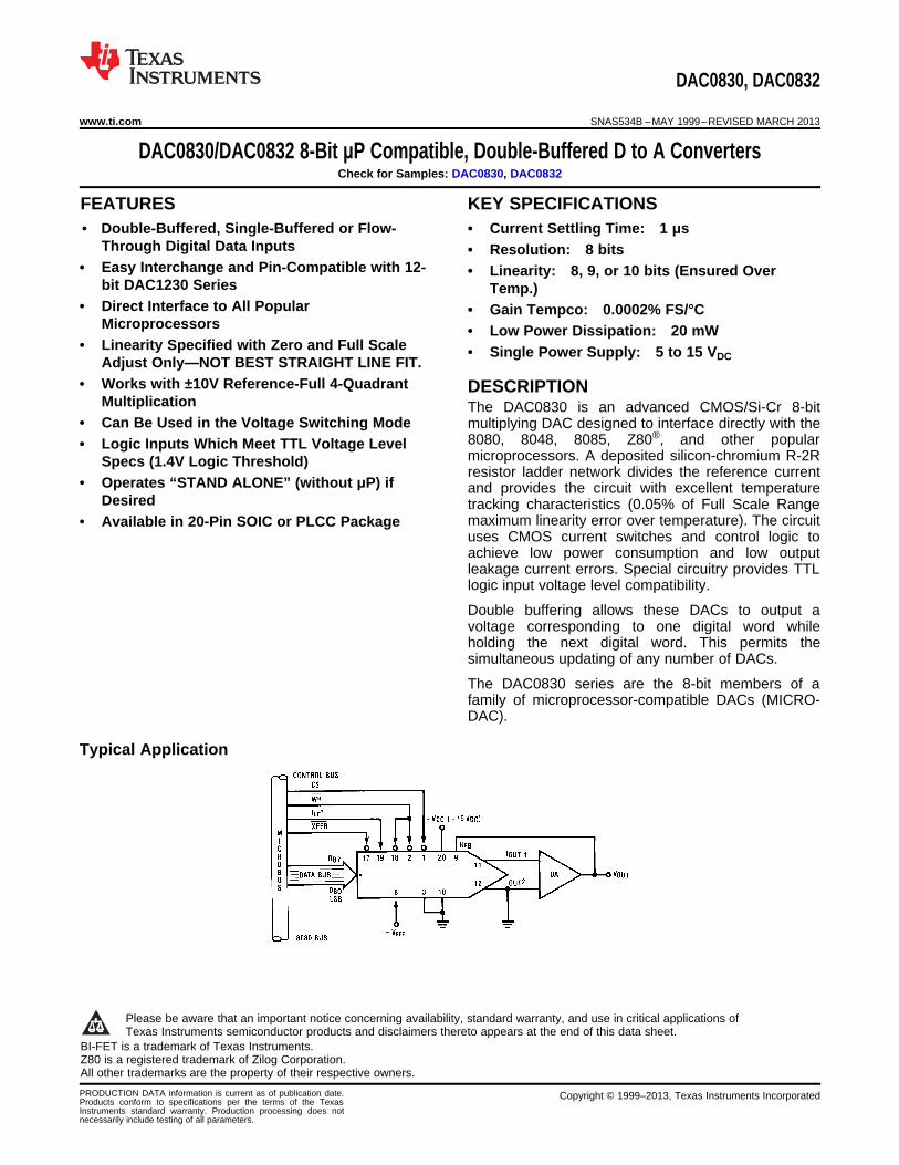
Typical Application
1
Please be aware that an important notice concerning availability, standard warranty, and use in critical applications ofTexas Instruments semiconductor products and disclaimers thereto appears at the end of this data sheet.
2BI-FET is a trademark of Texas Instruments.3Z80 is a registered trademark of Zilog Corporation.4All other trademarks are the property of their respective owners.
PRODUCTION DATA information is current as of publication date. Copyright © 1999–2013, Texas Instruments IncorporatedProducts conform to specifications per the terms of the TexasInstruments standard warranty. Production processing does notnecessarily include testing of all parameters.
DAC0830, DAC0832
SNAS534B –MAY 1999–REVISED MARCH 2013 www.ti.com
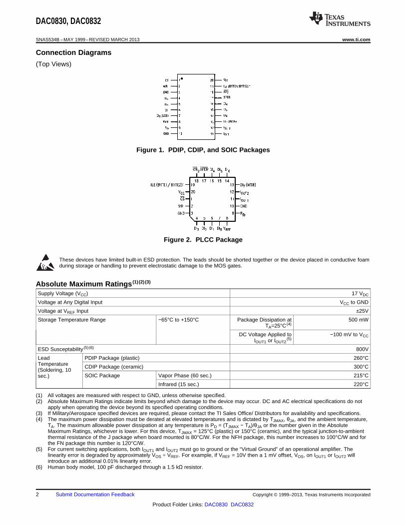
Connection Diagrams
(Top Views)
Figure 1. PDIP, CDIP, and SOIC Packages
Figure 2. PLCC Package
These devices have limited built-in ESD protection. The leads should be shorted together or the device placed in conductive foamduring storage or handling to prevent electrostatic damage to the MOS gates.
Absolute Maximum Ratings (1) (2) (3)
Supply Voltage (VCC) 17 VDC
Voltage at Any Digital Input VCC to GND
Voltage at VREF Input ±25V
Storage Temperature Range −65°C to +150°C Package Dissipation at 500 mWTA=25°C (4)
DC Voltage Applied to −100 mV to VCCIOUT1 or IOUT2
(5)
ESD Susceptability (5) (6) 800V
Lead PDIP Package (plastic) 260°CTemperature CDIP Package (ceramic) 300°C(Soldering, 10
SOIC Package Vapor Phase (60 sec.) 215°Csec.)
Infrared (15 sec.) 220°C
(1) All voltages are measured with respect to GND, unless otherwise specified.(2) Absolute Maximum Ratings indicate limits beyond which damage to the device may occur. DC and AC electrical specifications do not
apply when operating the device beyond its specified operating conditions.(3) If Military/Aerospace specified devices are required, please contact the TI Sales Office/ Distributors for availability and specifications.(4) The maximum power dissipation must be derated at elevated temperatures and is dictated by TJMAX, θJA, and the ambient temperature,
TA. The maximum allowable power dissipation at any temperature is PD = (TJMAX − TA)/θJA or the number given in the AbsoluteMaximum Ratings, whichever is lower. For this device, TJMAX = 125°C (plastic) or 150°C (ceramic), and the typical junction-to-ambientthermal resistance of the J package when board mounted is 80°C/W. For the NFH package, this number increases to 100°C/W and forthe FN package this number is 120°C/W.
(5) For current switching applications, both IOUT1 and IOUT2 must go to ground or the “Virtual Ground” of an operational amplifier. Thelinearity error is degraded by approximately VOS ÷ VREF. For example, if VREF = 10V then a 1 mV offset, VOS, on IOUT1 or IOUT2 willintroduce an additional 0.01% linearity error.
(6) Human body model, 100 pF discharged through a 1.5 kΩ resistor.
2 Submit Documentation Feedback Copyright © 1999–2013, Texas Instruments Incorporated
Product Folder Links: DAC0830 DAC0832

DAC0830, DAC0832
www.ti.com SNAS534B –MAY 1999–REVISED MARCH 2013
Operating ConditionsTemperature Range TMIN≤TA≤TMAX Part numbers with “LCN” suffix 0°C to +70°C
Part numbers with “LCWM” suffix 0°C to +70°C
Part numbers with “LCV” suffix 0°C to +70°C
Part numbers with “LCJ” suffix −40°C to +85°C
Part numbers with “LJ” suffix −55°C to +125°C
Voltage at Any Digital Input VCC to GND
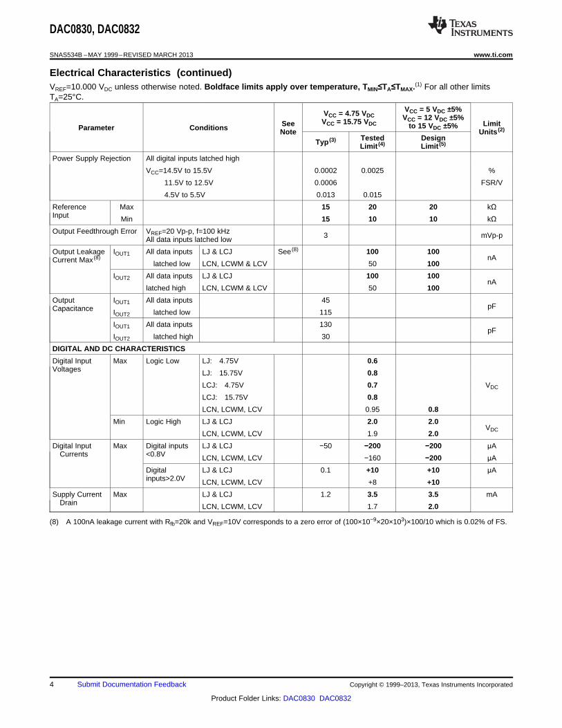
Electrical CharacteristicsVREF=10.000 VDC unless otherwise noted. Boldface limits apply over temperature, TMIN≤TA≤TMAX. (1) For all other limitsTA=25°C.
VCC = 5 VDC ±5%VCC = 4.75 VDC VCC = 12 VDC ±5%VCC = 15.75 VDCSee Limitto 15 VDC ±5%Parameter Conditions Note Units (2)
Tested DesignTyp (3)Limit (4) Limit (5)
CONVERTER CHARACTERISTICS
Resolution 8 8 8 bits
Linearity Error Max Zero and full scale adjusted See (6)
−10V≤VREF≤+10V and (2)
DAC0830LJ & LCJ 0.05 0.05 % FSR
DAC0832LJ & LCJ 0.2 0.2 % FSR
DAC0830LCN, LCWM & 0.05 0.05 % FSRLCV
DAC0831LCN 0.1 0.1 % FSR
DAC0832LCN, LCWM & 0.2 0.2 % FSRLCV
Differential Nonlinearity Zero and full scale adjusted See (6)
Max −10V≤VREF≤+10V and (2)
DAC0830LJ & LCJ 0.1 0.1 % FSR
DAC0832LJ & LCJ 0.4 0.4 % FSR
DAC0830LCN, LCWM & 0.1 0.1 % FSRLCV
DAC0831LCN 0.2 0.2 % FSR
DAC0832LCN, LCWM & 0.4 0.4 % FSRLCV
Monotonicity −10V≤VREF LJ & LCJ See (6) 8 8 bits
≤+10V LCN, LCWM & LCV 8 8 bits
Gain Error Max Using Internal Rfb See (7) ±0.2 ±1 ±1 % FS
−10V≤VREF≤+10V
%Gain Error Tempco Max Using internal Rfb 0.0002 0.0006 FS/°C
(1) Boldface tested limits apply to the LJ and LCJ suffix parts only.(2) The unit “FSR” stands for “Full Scale Range.” “Linearity Error” and “Power Supply Rejection” specs are based on this unit to eliminate
dependence on a particular VREF value and to indicate the true performance of the part. The “Linearity Error” specification of theDAC0830 is “0.05% of FSR (MAX)”. This ensures that after performing a zero and full scale adjustment (see sections Zero Adjustmentand Full-Scale Adjustment), the plot of the 256 analog voltage outputs will each be within 0.05%×VREF of a straight line which passesthrough zero and full scale.
(3) Typicals are at 25°C and represent most likely parametric norm.(4) Tested limits are ensured to TI's AOQL (Average Outgoing Quality Level).(5) Ensured, but not 100% production tested. These limits are not used to calculate outgoing quality levels.(6) For current switching applications, both IOUT1 and IOUT2 must go to ground or the “Virtual Ground” of an operational amplifier. The
linearity error is degraded by approximately VOS ÷ VREF. For example, if VREF = 10V then a 1 mV offset, VOS, on IOUT1 or IOUT2 willintroduce an additional 0.01% linearity error.
(7) Specified at VREF=±10 VDC and VREF=±1 VDC.
Copyright © 1999–2013, Texas Instruments Incorporated Submit Documentation Feedback 3
Product Folder Links: DAC0830 DAC0832
DAC0830, DAC0832
SNAS534B –MAY 1999–REVISED MARCH 2013 www.ti.com
Electrical Characteristics (continued)VREF=10.000 VDC unless otherwise noted. Boldface limits apply over temperature, TMIN≤TA≤TMAX.(1) For all other limitsTA=25°C.
VCC = 5 VDC ±5%VCC = 4.75 VDC VCC = 12 VDC ±5%VCC = 15.75 VDCSee Limitto 15 VDC ±5%Parameter Conditions Note Units (2)
Tested DesignTyp (3)Limit (4) Limit (5)
Power Supply Rejection All digital inputs latched high
VCC=14.5V to 15.5V 0.0002 0.0025 %
11.5V to 12.5V 0.0006 FSR/V
4.5V to 5.5V 0.013 0.015
Reference Max 15 20 20 kΩInput Min 15 10 10 kΩOutput Feedthrough Error VREF=20 Vp-p, f=100 kHz 3 mVp-pAll data inputs latched low
Output Leakage IOUT1 All data inputs LJ & LCJ See (8) 100 100nACurrent Max (8)
latched low LCN, LCWM & LCV 50 100
IOUT2 All data inputs LJ & LCJ 100 100nA
latched high LCN, LCWM & LCV 50 100
Output IOUT1 All data inputs 45pFCapacitance IOUT2 latched low 115
IOUT1 All data inputs 130pF
IOUT2 latched high 30
DIGITAL AND DC CHARACTERISTICS
Digital Input Max Logic Low LJ: 4.75V 0.6Voltages LJ: 15.75V 0.8
LCJ: 4.75V 0.7 VDC
LCJ: 15.75V 0.8
LCN, LCWM, LCV 0.95 0.8
Min Logic High LJ & LCJ 2.0 2.0VDC
LCN, LCWM, LCV 1.9 2.0
Digital Input Max Digital inputs LJ & LCJ −50 −200 −200 μACurrents <0.8V LCN, LCWM, LCV −160 −200 μA
Digital LJ & LCJ 0.1 +10 +10 μAinputs>2.0V LCN, LCWM, LCV +8 +10
Supply Current Max LJ & LCJ 1.2 3.5 3.5 mADrain LCN, LCWM, LCV 1.7 2.0
(8) A 100nA leakage current with Rfb=20k and VREF=10V corresponds to a zero error of (100×10−9×20×103)×100/10 which is 0.02% of FS.
4 Submit Documentation Feedback Copyright © 1999–2013, Texas Instruments Incorporated
Product Folder Links: DAC0830 DAC0832

DAC0830, DAC0832
www.ti.com SNAS534B –MAY 1999–REVISED MARCH 2013
Electrical CharacteristicsVREF=10.000 VDC unless otherwise noted. Boldface limits apply over temperature, TMIN≤TA≤TMAX. (1) For all other limitsTA=25°C.
VCC=12 VDC±5% VCC=5VCC=15.75 VDC VCC=4.75 VDCto 15 VDC ±5% VDC±5%See LimitSymbol Parameter Conditions Note UnitsTested Tested DesignTyp (2) Design Limit (4) Typ (2)Limit (3) Limit (3) Limit (4)
AC CHARACTERISTICS (5)
ts Current Setting VIL=0V, VIH=5V 1.0 1.0 μsTime
tW Write and XFER VIL=0V, VIH=5V See ( 100 250 375 6005)
Pulse Width Min See ( 320 320 900 9001)
tDS Data Setup Time VIL=0V, VIH=5V See ( 100 250 375 6001)
Min 320 320 900 900
tDH Data Hold Time VIL=0V, VIH=5V See ( 30 50 ns1)
Min 30 50
tCS Control Setup VIL=0V, VIH=5V See ( 110 250 600 900Time 1)
Min 320 320 1100 1100
tCH Control Hold Time VIL=0V, VIH=5V See ( 0 00 10 01)
Min 0 0
(1) Boldface tested limits apply to the LJ and LCJ suffix parts only.(2) Typicals are at 25°C and represent most likely parametric norm.(3) Tested limits are ensured to TI's AOQL (Average Outgoing Quality Level).(4) Ensured, but not 100% production tested. These limits are not used to calculate outgoing quality levels.(5) The entire write pulse must occur within the valid data interval for the specified tW, tDS, tDH, and tS to apply.
Switching Waveform
Definition of Package Pinouts
Control Signals
(All control signals level actuated)
CS: Chip Select (active low). The CS in combination with ILE will enable WR1.
ILE: Input Latch Enable (active high). The ILE in combination with CS enables WR1.
WR1: Write 1. The active low WR1 is used to load the digital input data bits (DI) into the input latch. The data inthe input latch is latched when WR1 is high. To update the input latch–CS and WR1 must be low while ILE
Copyright © 1999–2013, Texas Instruments Incorporated Submit Documentation Feedback 5
Product Folder Links: DAC0830 DAC0832

DAC0830, DAC0832
SNAS534B –MAY 1999–REVISED MARCH 2013 www.ti.com
is high.
WR2: Write 2 (active low). This signal, in combination with XFER, causes the 8-bit data which is available in theinput latch to transfer to the DAC register.
XFER: Transfer control signal (active low). The XFER will enable WR2.
Other Pin Functions
DI0-DI7: Digital Inputs. DI0 is the least significant bit (LSB) and DI7 is the most significant bit (MSB).
IOUT1: DAC Current Output 1. IOUT1 is a maximum for a digital code of all 1's in the DAC register, and is zero forall 0's in DAC register.
IOUT2: DAC Current Output 2. IOUT2 is a constant minus IOUT1 , or IOUT1 + IOUT2 = constant (I full scale for a fixedreference voltage).
Rfb: Feedback Resistor. The feedback resistor is provided on the IC chip for use as the shunt feedbackresistor for the external op amp which is used to provide an output voltage for the DAC. This on-chipresistor should always be used (not an external resistor) since it matches the resistors which are used inthe on-chip R-2R ladder and tracks these resistors over temperature.
VREF: Reference Voltage Input. This input connects an external precision voltage source to the internal R-2Rladder. VREF can be selected over the range of +10 to −10V. This is also the analog voltage input for a 4-quadrant multiplying DAC application.
VCC: Digital Supply Voltage. This is the power supply pin for the part. VCC can be from +5 to +15VDC.Operation is optimum for +15VDC
GND: The pin 10 voltage must be at the same ground potential as IOUT1 and IOUT2 for current switchingapplications. Any difference of potential (VOS pin 10) will result in a linearity change of :
(1)
For example, if VREF = 10V and pin 10 is 9mV offset from IOUT1 and IOUT2 the linearity change will be 0.03%.
Pin 3 can be offset ±100mV with no linearity change, but the logic input threshold will shift.
Linearity Error
Figure 3. a) End Point Test After Figure 4. b) Best Straight Line Figure 5. c) Shifting fs adj. toZero and fs adj. Pass
Best Straight Line Test
Definition of Terms
Resolution: Resolution is directly related to the number of switches or bits within the DAC. For example, theDAC0830 has 28 or 256 steps and therefore has 8-bit resolution.
Linearity Error: Linearity Error is the maximum deviation from a straight line passing through the endpoints ofthe DAC transfer characteristic. It is measured after adjusting for zero and full-scale. Linearity error is aparameter intrinsic to the device and cannot be externally adjusted.
6 Submit Documentation Feedback Copyright © 1999–2013, Texas Instruments Incorporated
Product Folder Links: DAC0830 DAC0832

DAC0830, DAC0832
www.ti.com SNAS534B –MAY 1999–REVISED MARCH 2013
TI's linearity “end point test” (a) and the “best straight line” test (b,c) used by other suppliers are illustrated above.The “end point test'' greatly simplifies the adjustment procedure by eliminating the need for multiple iterations ofchecking the linearity and then adjusting full scale until the linearity is met. The “end point test'' ensures thatlinearity is met after a single full scale adjust. (One adjustment vs. multiple iterations of the adjustment.) The “endpoint test'' uses a standard zero and F.S. adjustment procedure and is a much more stringent test for DAClinearity.
Power Supply Sensitivity: Power supply sensitivity is a measure of the effect of power supply changes on theDAC full-scale output.
Settling Time: Settling time is the time required from a code transition until the DAC output reaches within±½LSB of the final output value. Full-scale settling time requires a zero to full-scale or full-scale to zero outputchange.
Full Scale Error: Full scale error is a measure of the output error between an ideal DAC and the actual deviceoutput. Ideally, for the DAC0830 series, full scale is VREF −1LSB. For VREF = 10V and unipolar operation, VFULL-
SCALE = 10,0000V–39mV 9.961V. Full-scale error is adjustable to zero.
Differential Nonlinearity: The difference between any two consecutive codes in the transfer curve from thetheoretical 1 LSB to differential nonlinearity.
Monotonic: If the output of a DAC increases for increasing digital input code, then the DAC is monotonic. An 8-bit DAC which is monotonic to 8 bits simply means that increasing digital input codes will produce an increasinganalog output.
Figure 6. DAC0830 Functional Diagram
Copyright © 1999–2013, Texas Instruments Incorporated Submit Documentation Feedback 7
Product Folder Links: DAC0830 DAC0832

DAC0830, DAC0832
SNAS534B –MAY 1999–REVISED MARCH 2013 www.ti.com
Typical Performance Characteristics
Digital Input Threshold Digital Input Thresholdvs. vs.
Temperature VCC
Figure 7. Figure 8.
Gain and Linearity Error Variation Gain and Linearity Error Variationvs. vs.
Temperature Supply Voltage
Figure 9. Figure 10.
Write Pulse Width Data Hold Time
Figure 11. Figure 12.
8 Submit Documentation Feedback Copyright © 1999–2013, Texas Instruments Incorporated
Product Folder Links: DAC0830 DAC0832

DAC0830, DAC0832
www.ti.com SNAS534B –MAY 1999–REVISED MARCH 2013
DAC0830 SERIES APPLICATION HINTS
These DAC's are the industry's first microprocessor compatible, double-buffered 8-bit multiplying D to Aconverters. Double-buffering allows the utmost application flexibility from a digital control point of view. This 20-pin device is also pin for pin compatible (with one exception) with the DAC1230, a 12-bit MICRO-DAC. In theevent that a system's analog output resolution and accuracy must be upgraded, substituting the DAC1230 canbe easily accomplished. By tying address bit A0 to the ILE pin, a two-byte μP write instruction (double precision)which automatically increments the address for the second byte write (starting with A0=“1”) can be used. Thisallows either an 8-bit or the 12-bit part to be used with no hardware or software changes. For the simplest 8-bitapplication, this pin should be tied to VCC (also see other uses in Double-Buffered Operation).
Analog signal control versatility is provided by a precision R-2R ladder network which allows full 4-quadrantmultiplication of a wide range bipolar reference voltage by an applied digital word.
DIGITAL CONSIDERATIONS
A most unique characteristic of these DAC's is that the 8-bit digital input byte is double-buffered. This means thatthe data must transfer through two independently controlled 8-bit latching registers before being applied to the R-2R ladder network to change the analog output. The addition of a second register allows two useful controlfeatures. First, any DAC in a system can simultaneously hold the current DAC data in one register (DAC register)and the next data word in the second register (input register) to allow fast updating of the DAC output ondemand. Second, and probably more important, double-buffering allows any number of DAC's in a system to beupdated to their new analog output levels simultaneously via a common strobe signal.
The timing requirements and logic level convention of the register control signals have been designed tominimize or eliminate external interfacing logic when applied to most popular microprocessors and developmentsystems. It is easy to think of these converters as 8-bit “write-only” memory locations that provide an analogoutput quantity. All inputs to these DAC's meet TTL voltage level specs and can also be driven directly with highvoltage CMOS logic in non-microprocessor based systems. To prevent damage to the chip from static discharge,all unused digital inputs should be tied to VCC or ground. If any of the digital inputs are inadvertantly left floating,the DAC interprets the pin as a logic “1”.
Double-Buffered Operation
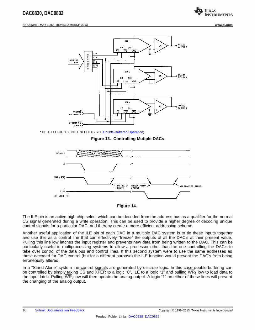
Updating the analog output of these DAC's in a double-buffered manner is basically a two step or double writeoperation. In a microprocessor system two unique system addresses must be decoded, one for the input latchcontrolled by the CS pin and a second for the DAC latch which is controlled by the XFER line. If more than oneDAC is being driven, Figure 13, the CS line of each DAC would typically be decoded individually, but all of theconverters could share a common XFER address to allow simultaneous updating of any number of DAC's. Thetiming for this operation is shown, Figure 14.
It is important to note that the analog outputs that will change after a simultaneous transfer are those from theDAC's whose input register had been modified prior to the XFER command.
Copyright © 1999–2013, Texas Instruments Incorporated Submit Documentation Feedback 9
Product Folder Links: DAC0830 DAC0832
DAC0830, DAC0832
SNAS534B –MAY 1999–REVISED MARCH 2013 www.ti.com
*TIE TO LOGIC 1 IF NOT NEEDED (SEE Double-Buffered Operation).
Figure 13. Controlling Mutiple DACs
Figure 14.
The ILE pin is an active high chip select which can be decoded from the address bus as a qualifier for the normalCS signal generated during a write operation. This can be used to provide a higher degree of decoding uniquecontrol signals for a particular DAC, and thereby create a more efficient addressing scheme.
Another useful application of the ILE pin of each DAC in a multiple DAC system is to tie these inputs togetherand use this as a control line that can effectively “freeze” the outputs of all the DAC's at their present value.Pulling this line low latches the input register and prevents new data from being written to the DAC. This can beparticularly useful in multiprocessing systems to allow a processor other than the one controlling the DAC's totake over control of the data bus and control lines. If this second system were to use the same addresses asthose decoded for DAC control (but for a different purpose) the ILE function would prevent the DAC's from beingerroneously altered.
In a “Stand-Alone” system the control signals are generated by discrete logic. In this case double-buffering canbe controlled by simply taking CS and XFER to a logic “0”, ILE to a logic “1” and pulling WR1 low to load data tothe input latch. Pulling WR2 low will then update the analog output. A logic “1” on either of these lines will preventthe changing of the analog output.
10 Submit Documentation Feedback Copyright © 1999–2013, Texas Instruments Incorporated
Product Folder Links: DAC0830 DAC0832
DAC0830, DAC0832
www.ti.com SNAS534B –MAY 1999–REVISED MARCH 2013
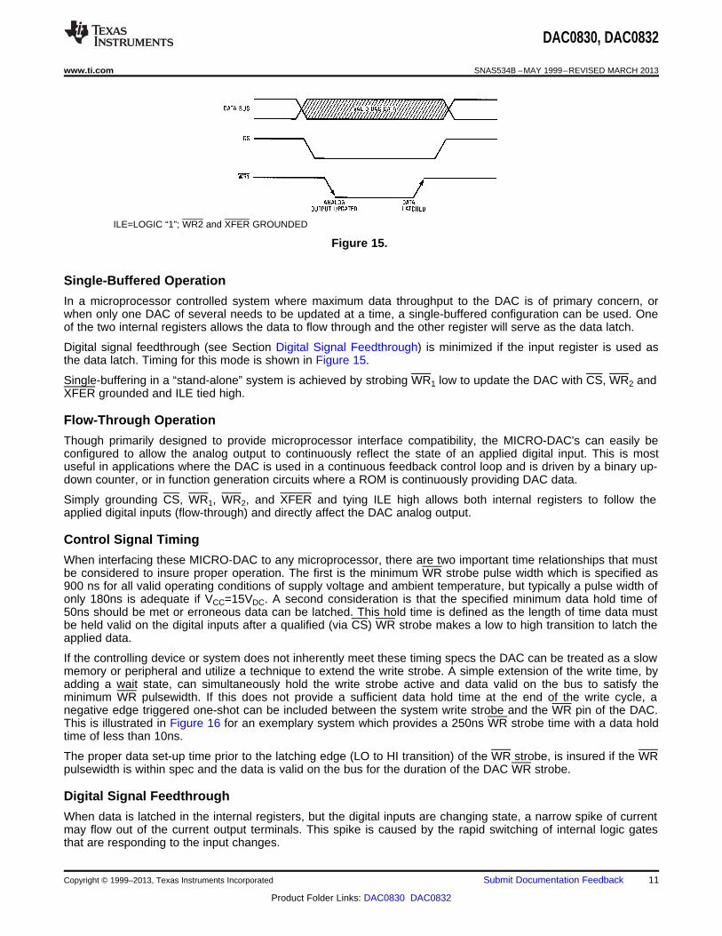
ILE=LOGIC “1”; WR2 and XFER GROUNDED
Figure 15.
Single-Buffered Operation
In a microprocessor controlled system where maximum data throughput to the DAC is of primary concern, orwhen only one DAC of several needs to be updated at a time, a single-buffered configuration can be used. Oneof the two internal registers allows the data to flow through and the other register will serve as the data latch.
Digital signal feedthrough (see Section Digital Signal Feedthrough) is minimized if the input register is used asthe data latch. Timing for this mode is shown in Figure 15.
Single-buffering in a “stand-alone” system is achieved by strobing WR1 low to update the DAC with CS, WR2 andXFER grounded and ILE tied high.
Flow-Through Operation
Though primarily designed to provide microprocessor interface compatibility, the MICRO-DAC's can easily beconfigured to allow the analog output to continuously reflect the state of an applied digital input. This is mostuseful in applications where the DAC is used in a continuous feedback control loop and is driven by a binary up-down counter, or in function generation circuits where a ROM is continuously providing DAC data.
Simply grounding CS, WR1, WR2, and XFER and tying ILE high allows both internal registers to follow theapplied digital inputs (flow-through) and directly affect the DAC analog output.
Control Signal Timing
When interfacing these MICRO-DAC to any microprocessor, there are two important time relationships that mustbe considered to insure proper operation. The first is the minimum WR strobe pulse width which is specified as900 ns for all valid operating conditions of supply voltage and ambient temperature, but typically a pulse width ofonly 180ns is adequate if VCC=15VDC. A second consideration is that the specified minimum data hold time of50ns should be met or erroneous data can be latched. This hold time is defined as the length of time data mustbe held valid on the digital inputs after a qualified (via CS) WR strobe makes a low to high transition to latch theapplied data.
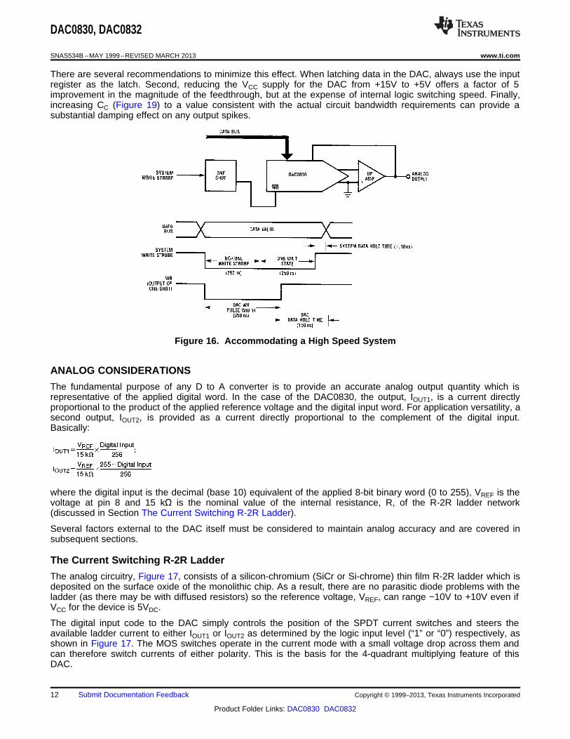
If the controlling device or system does not inherently meet these timing specs the DAC can be treated as a slowmemory or peripheral and utilize a technique to extend the write strobe. A simple extension of the write time, byadding a wait state, can simultaneously hold the write strobe active and data valid on the bus to satisfy theminimum WR pulsewidth. If this does not provide a sufficient data hold time at the end of the write cycle, anegative edge triggered one-shot can be included between the system write strobe and the WR pin of the DAC.This is illustrated in Figure 16 for an exemplary system which provides a 250ns WR strobe time with a data holdtime of less than 10ns.
The proper data set-up time prior to the latching edge (LO to HI transition) of the WR strobe, is insured if the WRpulsewidth is within spec and the data is valid on the bus for the duration of the DAC WR strobe.
Digital Signal Feedthrough
When data is latched in the internal registers, but the digital inputs are changing state, a narrow spike of currentmay flow out of the current output terminals. This spike is caused by the rapid switching of internal logic gatesthat are responding to the input changes.
Copyright © 1999–2013, Texas Instruments Incorporated Submit Documentation Feedback 11
Product Folder Links: DAC0830 DAC0832
DAC0830, DAC0832
SNAS534B –MAY 1999–REVISED MARCH 2013 www.ti.com
There are several recommendations to minimize this effect. When latching data in the DAC, always use the inputregister as the latch. Second, reducing the VCC supply for the DAC from +15V to +5V offers a factor of 5improvement in the magnitude of the feedthrough, but at the expense of internal logic switching speed. Finally,increasing CC (Figure 19) to a value consistent with the actual circuit bandwidth requirements can provide asubstantial damping effect on any output spikes.
Figure 16. Accommodating a High Speed System
ANALOG CONSIDERATIONS
The fundamental purpose of any D to A converter is to provide an accurate analog output quantity which isrepresentative of the applied digital word. In the case of the DAC0830, the output, IOUT1, is a current directlyproportional to the product of the applied reference voltage and the digital input word. For application versatility, asecond output, IOUT2, is provided as a current directly proportional to the complement of the digital input.Basically:
where the digital input is the decimal (base 10) equivalent of the applied 8-bit binary word (0 to 255), VREF is thevoltage at pin 8 and 15 kΩ is the nominal value of the internal resistance, R, of the R-2R ladder network(discussed in Section The Current Switching R-2R Ladder).
Several factors external to the DAC itself must be considered to maintain analog accuracy and are covered insubsequent sections.
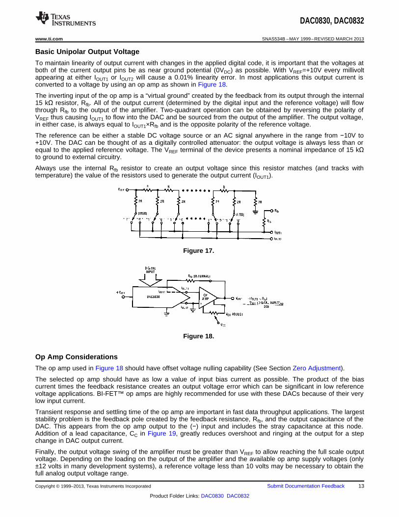
The Current Switching R-2R Ladder
The analog circuitry, Figure 17, consists of a silicon-chromium (SiCr or Si-chrome) thin film R-2R ladder which isdeposited on the surface oxide of the monolithic chip. As a result, there are no parasitic diode problems with theladder (as there may be with diffused resistors) so the reference voltage, VREF, can range −10V to +10V even ifVCC for the device is 5VDC.
The digital input code to the DAC simply controls the position of the SPDT current switches and steers theavailable ladder current to either IOUT1 or IOUT2 as determined by the logic input level (“1” or “0”) respectively, asshown in Figure 17. The MOS switches operate in the current mode with a small voltage drop across them andcan therefore switch currents of either polarity. This is the basis for the 4-quadrant multiplying feature of thisDAC.
12 Submit Documentation Feedback Copyright © 1999–2013, Texas Instruments Incorporated
Product Folder Links: DAC0830 DAC0832
DAC0830, DAC0832
www.ti.com SNAS534B –MAY 1999–REVISED MARCH 2013
Basic Unipolar Output Voltage
To maintain linearity of output current with changes in the applied digital code, it is important that the voltages atboth of the current output pins be as near ground potential (0VDC) as possible. With VREF=+10V every millivoltappearing at either IOUT1 or IOUT2 will cause a 0.01% linearity error. In most applications this output current isconverted to a voltage by using an op amp as shown in Figure 18.
The inverting input of the op amp is a “virtual ground” created by the feedback from its output through the internal15 kΩ resistor, Rfb. All of the output current (determined by the digital input and the reference voltage) will flowthrough Rfb to the output of the amplifier. Two-quadrant operation can be obtained by reversing the polarity ofVREF thus causing IOUT1 to flow into the DAC and be sourced from the output of the amplifier. The output voltage,in either case, is always equal to IOUT1×Rfb and is the opposite polarity of the reference voltage.
The reference can be either a stable DC voltage source or an AC signal anywhere in the range from −10V to+10V. The DAC can be thought of as a digitally controlled attenuator: the output voltage is always less than orequal to the applied reference voltage. The VREF terminal of the device presents a nominal impedance of 15 kΩto ground to external circuitry.
Always use the internal Rfb resistor to create an output voltage since this resistor matches (and tracks withtemperature) the value of the resistors used to generate the output current (IOUT1).
Figure 17.
Figure 18.
Op Amp Considerations
The op amp used in Figure 18 should have offset voltage nulling capability (See Section Zero Adjustment).
The selected op amp should have as low a value of input bias current as possible. The product of the biascurrent times the feedback resistance creates an output voltage error which can be significant in low referencevoltage applications. BI-FET™ op amps are highly recommended for use with these DACs because of their verylow input current.
Transient response and settling time of the op amp are important in fast data throughput applications. The largeststability problem is the feedback pole created by the feedback resistance, Rfb, and the output capacitance of theDAC. This appears from the op amp output to the (−) input and includes the stray capacitance at this node.Addition of a lead capacitance, CC in Figure 19, greatly reduces overshoot and ringing at the output for a stepchange in DAC output current.
Finally, the output voltage swing of the amplifier must be greater than VREF to allow reaching the full scale outputvoltage. Depending on the loading on the output of the amplifier and the available op amp supply voltages (only±12 volts in many development systems), a reference voltage less than 10 volts may be necessary to obtain thefull analog output voltage range.
Copyright © 1999–2013, Texas Instruments Incorporated Submit Documentation Feedback 13
Product Folder Links: DAC0830 DAC0832

DAC0830, DAC0832
SNAS534B –MAY 1999–REVISED MARCH 2013 www.ti.com
Bipolar Output Voltage with a Fixed Reference
The addition of a second op amp to the previous circuitry can be used to generate a bipolar output voltage froma fixed reference voltage. This, in effect, gives sign significance to the MSB of the digital input word and allowstwo-quadrant multiplication of the reference voltage. The polarity of the reference can also be reversed to realizefull 4-quadrant multiplication: ±VREF×±Digital Code=±VOUT. This circuit is shown in Figure 20.
This configuration features several improvements over existing circuits for bipolar outputs with other multiplyingDACs. Only the offset voltage of amplifier 1 has to be nulled to preserve linearity of the DAC. The offset voltageerror of the second op amp (although a constant output voltage error) has no effect on linearity. It should benulled only if absolute output accuracy is required. Finally, the values of the resistors around the second amplifierdo not have to match the internal DAC resistors, they need only to match and temperature track each other. Athin film 4-resistor network available from Beckman Instruments, Inc. (part no. 694-3-R10K-D) is ideally suited forthis application. These resistors are matched to 0.1% and exhibit only 5 ppm/°C resistance tracking temperaturecoefficient. Two of the four available 10 kΩ resistors can be paralleled to form R in Figure 20 and the other twocan be used independently as the resistances labeled 2R.
Zero Adjustment
For accurate conversions, the input offset voltage of the output amplifier must always be nulled. Amplifier offseterrors create an overall degradation of DAC linearity.
The fundamental purpose of zeroing is to make the voltage appearing at the DAC outputs as near 0VDC aspossible. This is accomplished for the typical DAC — op amp connection (Figure 18) by shorting out Rfb, theamplifier feedback resistor, and adjusting the VOS nulling potentiometer of the op amp until the output reads zerovolts. This is done, of course, with an applied digital code of all zeros if IOUT1 is driving the op amp (all one's forIOUT2). The short around Rfb is then removed and the converter is zero adjusted.
Figure 19.
tsOP Amp CC (O to Full Scale)
LF356 22 pF 4 μs
LF351 22 pF 5 μs
LF357 (1) 10 pF 2 μs
(1) 2.4 kΩ RESISTOR ADDED FROM−INPUT TO GROUND TOINSURE STABILITY
*THESE RESISTORS ARE AVAILABLE FROM BECKMAN INSTRUMENTS, INC. AS THEIR PART NO. 694-3-R10K-D
Figure 20.
14 Submit Documentation Feedback Copyright © 1999–2013, Texas Instruments Incorporated
Product Folder Links: DAC0830 DAC0832

DAC0830, DAC0832
www.ti.com SNAS534B –MAY 1999–REVISED MARCH 2013
Input Code IDEAL VOUT
MSB LSB +VREF −VREF
1 1 1 1 1 1 1 1
1 1 0 0 0 0 0 0
1 0 0 0 0 0 0 0
0 1 1 1 1 1 1 1
0 0 1 1 1 1 1 1
0 0 0 0 0 0 0 0
Full-Scale Adjustment
In the case where the matching of Rfb to the R value of the R-2R ladder (typically ±0.2%) is insufficient for full-scale accuracy in a particular application, the VREF voltage can be adjusted or an external resistor andpotentiometer can be added as shown in Figure 21 to provide a full-scale adjustment.
The temperature coefficients of the resistors used for this adjustment are of an important concern. To preventdegradation of the gain error temperature coefficient by the external resistors, their temperature coefficientsideally would have to match that of the internal DAC resistors, which is a highly impractical constraint. For thevalues shown in Figure 21, if the resistor and the potentiometer each had a temperature coefficient of ±100ppm/°C maximum, the overall gain error temperature coefficent would be degraded a maximum of 0.0025%/°Cfor an adjustment pot setting of less than 3% of Rfb.
Using the DAC0830 in a Voltage Switching Configuration
The R-2R ladder can also be operated as a voltage switching network. In this mode the ladder is used in aninverted manner from the standard current switching configuration. The reference voltage is connected to one ofthe current output terminals (IOUT1 for true binary digital control, IOUT2 is for complementary binary) and the outputvoltage is taken from the normal VREF pin. The converter output is now a voltage in the range from 0V to 255/256VREF as a function of the applied digital code as shown in Figure 22.
Figure 21. Adding Full-Scale Adjustment
Figure 22. Voltage Mode Switching
Copyright © 1999–2013, Texas Instruments Incorporated Submit Documentation Feedback 15
Product Folder Links: DAC0830 DAC0832
DAC0830, DAC0832
SNAS534B –MAY 1999–REVISED MARCH 2013 www.ti.com
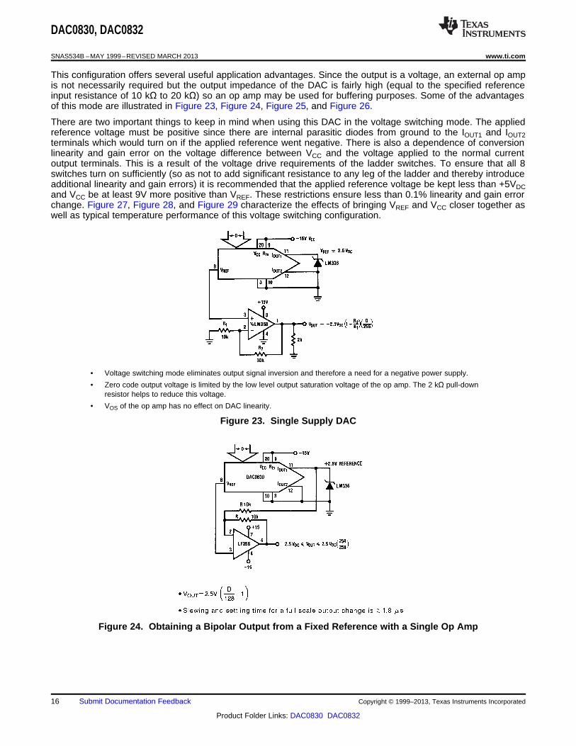
This configuration offers several useful application advantages. Since the output is a voltage, an external op ampis not necessarily required but the output impedance of the DAC is fairly high (equal to the specified referenceinput resistance of 10 kΩ to 20 kΩ) so an op amp may be used for buffering purposes. Some of the advantagesof this mode are illustrated in Figure 23, Figure 24, Figure 25, and Figure 26.
There are two important things to keep in mind when using this DAC in the voltage switching mode. The appliedreference voltage must be positive since there are internal parasitic diodes from ground to the IOUT1 and IOUT2terminals which would turn on if the applied reference went negative. There is also a dependence of conversionlinearity and gain error on the voltage difference between VCC and the voltage applied to the normal currentoutput terminals. This is a result of the voltage drive requirements of the ladder switches. To ensure that all 8switches turn on sufficiently (so as not to add significant resistance to any leg of the ladder and thereby introduceadditional linearity and gain errors) it is recommended that the applied reference voltage be kept less than +5VDCand VCC be at least 9V more positive than VREF. These restrictions ensure less than 0.1% linearity and gain errorchange. Figure 27, Figure 28, and Figure 29 characterize the effects of bringing VREF and VCC closer together aswell as typical temperature performance of this voltage switching configuration.
• Voltage switching mode eliminates output signal inversion and therefore a need for a negative power supply.
• Zero code output voltage is limited by the low level output saturation voltage of the op amp. The 2 kΩ pull-downresistor helps to reduce this voltage.
• VOS of the op amp has no effect on DAC linearity.
Figure 23. Single Supply DAC
Figure 24. Obtaining a Bipolar Output from a Fixed Reference with a Single Op Amp
16 Submit Documentation Feedback Copyright © 1999–2013, Texas Instruments Incorporated
Product Folder Links: DAC0830 DAC0832
DAC0830, DAC0832
www.ti.com SNAS534B –MAY 1999–REVISED MARCH 2013
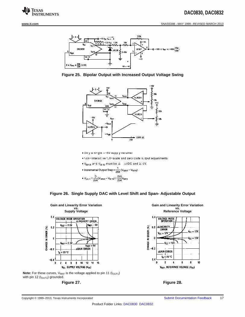
Figure 25. Bipolar Output with Increased Output Voltage Swing
Figure 26. Single Supply DAC with Level Shift and Span- Adjustable Output
Gain and Linearity Error Variation Gain and Linearity Error Variationvs. vs.
Supply Voltage Reference Voltage
Note: For these curves, VREF is the voltage applied to pin 11 (IOUT1)with pin 12 (IOUT2) grounded.
Figure 27. Figure 28.
Copyright © 1999–2013, Texas Instruments Incorporated Submit Documentation Feedback 17
Product Folder Links: DAC0830 DAC0832
DAC0830, DAC0832
SNAS534B –MAY 1999–REVISED MARCH 2013 www.ti.com
Gain and Linearity Error Variationvs.
Temperature
Figure 29.
Miscellaneous Application Hints
These converters are CMOS products and reasonable care should be exercised in handling them to preventcatastrophic failures due to static discharge.
Conversion accuracy is only as good as the applied reference voltage so providing a stable source over time andtemperature changes is an important factor to consider.
A “good” ground is most desirable. A single point ground distribution technique for analog signals and supplyreturns keeps other devices in a system from affecting the output of the DACs.
During power-up supply voltage sequencing, the −15V (or −12V) supply of the op amp may appear first. This willcause the output of the op amp to bias near the negative supply potential. No harm is done to the DAC, however,as the on-chip 15 kΩ feedback resistor sufficiently limits the current flow from IOUT1 when this lead is internallyclamped to one diode drop below ground.
Careful circuit construction with minimization of lead lengths around the analog circuitry, is a primary concern.Good high frequency supply decoupling will aid in preventing inadvertant noise from appearing on the analogoutput.
Overall noise reduction and reference stability is of particular concern when using the higher accuracy versions,the DAC0830 and DAC0831, or their advantages are wasted.
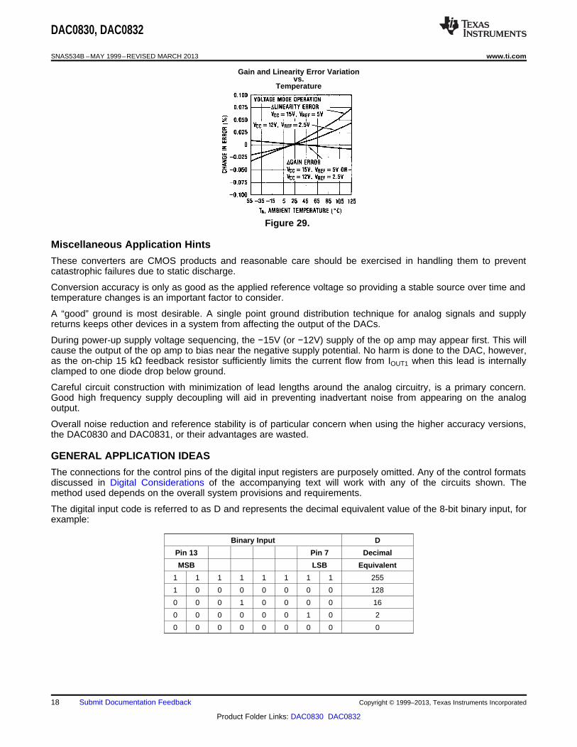
GENERAL APPLICATION IDEAS
The connections for the control pins of the digital input registers are purposely omitted. Any of the control formatsdiscussed in Digital Considerations of the accompanying text will work with any of the circuits shown. Themethod used depends on the overall system provisions and requirements.
The digital input code is referred to as D and represents the decimal equivalent value of the 8-bit binary input, forexample:
Binary Input D
Pin 13 Pin 7 Decimal
MSB LSB Equivalent
1 1 1 1 1 1 1 1 255
1 0 0 0 0 0 0 0 128
0 0 0 1 0 0 0 0 16
0 0 0 0 0 0 1 0 2
0 0 0 0 0 0 0 0 0
18 Submit Documentation Feedback Copyright © 1999–2013, Texas Instruments Incorporated
Product Folder Links: DAC0830 DAC0832
DAC0830, DAC0832
www.ti.com SNAS534B –MAY 1999–REVISED MARCH 2013
Applications
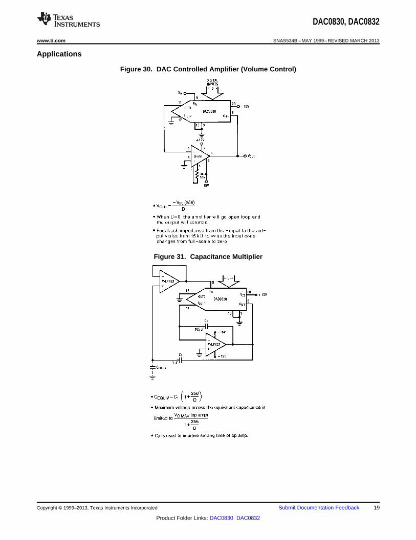
Figure 30. DAC Controlled Amplifier (Volume Control)
Figure 31. Capacitance Multiplier
Copyright © 1999–2013, Texas Instruments Incorporated Submit Documentation Feedback 19
Product Folder Links: DAC0830 DAC0832

DAC0830, DAC0832
SNAS534B –MAY 1999–REVISED MARCH 2013 www.ti.com
Figure 32. Variable fO, Variable QO, Constant BW Bandpass Filter
Figure 33. DAC Controlled Function Generator
20 Submit Documentation Feedback Copyright © 1999–2013, Texas Instruments Incorporated
Product Folder Links: DAC0830 DAC0832
DAC0830, DAC0832
www.ti.com SNAS534B –MAY 1999–REVISED MARCH 2013
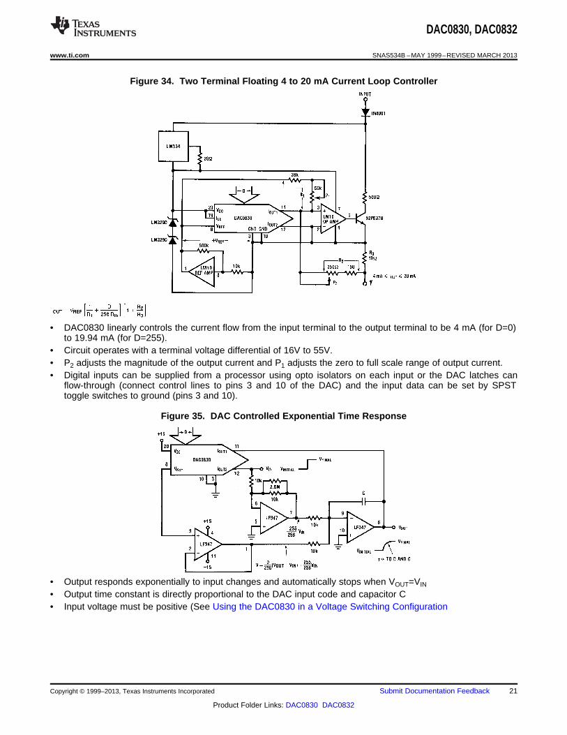
Figure 34. Two Terminal Floating 4 to 20 mA Current Loop Controller
• DAC0830 linearly controls the current flow from the input terminal to the output terminal to be 4 mA (for D=0)to 19.94 mA (for D=255).
• Circuit operates with a terminal voltage differential of 16V to 55V.• P2 adjusts the magnitude of the output current and P1 adjusts the zero to full scale range of output current.• Digital inputs can be supplied from a processor using opto isolators on each input or the DAC latches can
flow-through (connect control lines to pins 3 and 10 of the DAC) and the input data can be set by SPSTtoggle switches to ground (pins 3 and 10).
Figure 35. DAC Controlled Exponential Time Response
• Output responds exponentially to input changes and automatically stops when VOUT=VIN
• Output time constant is directly proportional to the DAC input code and capacitor C• Input voltage must be positive (See Using the DAC0830 in a Voltage Switching Configuration
Copyright © 1999–2013, Texas Instruments Incorporated Submit Documentation Feedback 21
Product Folder Links: DAC0830 DAC0832

DAC0830, DAC0832
SNAS534B –MAY 1999–REVISED MARCH 2013 www.ti.com
REVISION HISTORY
Changes from Revision A (March 2013) to Revision B Page
• Changed layout of National Data Sheet to TI format .......................................................................................................... 21
22 Submit Documentation Feedback Copyright © 1999–2013, Texas Instruments Incorporated
Product Folder Links: DAC0830 DAC0832

PACKAGE OPTION ADDENDUM
www.ti.com 22-Dec-2017
Addendum-Page 1
PACKAGING INFORMATION
Orderable Device Status(1)
Package Type PackageDrawing
Pins PackageQty
Eco Plan(2)
Lead/Ball Finish(6)
MSL Peak Temp(3)
Op Temp (°C) Device Marking(4/5)
Samples
DAC0830LCN LIFEBUY PDIP NFH 20 18 TBD Call TI Call TI 0 to 70 DAC0830LCN
DAC0830LCN/NOPB LIFEBUY PDIP NFH 20 18 Pb-Free(RoHS)
CU SN Level-1-NA-UNLIM 0 to 70 DAC0830LCN
DAC0832LCN LIFEBUY PDIP NFH 20 18 TBD Call TI Call TI 0 to 70 DAC0832LCN
DAC0832LCN/NOPB LIFEBUY PDIP NFH 20 18 Green (RoHS& no Sb/Br)
CU SN Level-1-NA-UNLIM 0 to 70 DAC0832LCN
DAC0832LCWM LIFEBUY SOIC DW 20 36 TBD Call TI Call TI 0 to 70 DAC0832LCWM
DAC0832LCWM/NOPB ACTIVE SOIC DW 20 36 Green (RoHS& no Sb/Br)
CU SN Level-3-260C-168 HR 0 to 70 DAC0832LCWM
DAC0832LCWMX LIFEBUY SOIC DW 20 1000 TBD Call TI Call TI 0 to 70 DAC0832LCWM
DAC0832LCWMX/NOPB ACTIVE SOIC DW 20 1000 Green (RoHS& no Sb/Br)
CU SN Level-3-260C-168 HR 0 to 70 DAC0832LCWM
(1) The marketing status values are defined as follows:ACTIVE: Product device recommended for new designs.LIFEBUY: TI has announced that the device will be discontinued, and a lifetime-buy period is in effect.NRND: Not recommended for new designs. Device is in production to support existing customers, but TI does not recommend using this part in a new design.PREVIEW: Device has been announced but is not in production. Samples may or may not be available.OBSOLETE: TI has discontinued the production of the device.
(2) RoHS: TI defines "RoHS" to mean semiconductor products that are compliant with the current EU RoHS requirements for all 10 RoHS substances, including the requirement that RoHS substancedo not exceed 0.1% by weight in homogeneous materials. Where designed to be soldered at high temperatures, "RoHS" products are suitable for use in specified lead-free processes. TI mayreference these types of products as "Pb-Free".RoHS Exempt: TI defines "RoHS Exempt" to mean products that contain lead but are compliant with EU RoHS pursuant to a specific EU RoHS exemption.Green: TI defines "Green" to mean the content of Chlorine (Cl) and Bromine (Br) based flame retardants meet JS709B low halogen requirements of <=1000ppm threshold. Antimony trioxide basedflame retardants must also meet the <=1000ppm threshold requirement.
(3) MSL, Peak Temp. - The Moisture Sensitivity Level rating according to the JEDEC industry standard classifications, and peak solder temperature.
(4) There may be additional marking, which relates to the logo, the lot trace code information, or the environmental category on the device.
(5) Multiple Device Markings will be inside parentheses. Only one Device Marking contained in parentheses and separated by a "~" will appear on a device. If a line is indented then it is a continuationof the previous line and the two combined represent the entire Device Marking for that device.

PACKAGE OPTION ADDENDUM
www.ti.com 22-Dec-2017
Addendum-Page 2
(6) Lead/Ball Finish - Orderable Devices may have multiple material finish options. Finish options are separated by a vertical ruled line. Lead/Ball Finish values may wrap to two lines if the finishvalue exceeds the maximum column width.
Important Information and Disclaimer:The information provided on this page represents TI's knowledge and belief as of the date that it is provided. TI bases its knowledge and belief on informationprovided by third parties, and makes no representation or warranty as to the accuracy of such information. Efforts are underway to better integrate information from third parties. TI has taken andcontinues to take reasonable steps to provide representative and accurate information but may not have conducted destructive testing or chemical analysis on incoming materials and chemicals.TI and TI suppliers consider certain information to be proprietary, and thus CAS numbers and other limited information may not be available for release.
In no event shall TI's liability arising out of such information exceed the total purchase price of the TI part(s) at issue in this document sold by TI to Customer on an annual basis.

TAPE AND REEL INFORMATION
*All dimensions are nominal
Device PackageType
PackageDrawing
Pins SPQ ReelDiameter
(mm)
ReelWidth
W1 (mm)
A0(mm)
B0(mm)
K0(mm)
P1(mm)
W(mm)
Pin1Quadrant
DAC0832LCWMX SOIC DW 20 1000 330.0 24.4 10.9 13.3 3.25 12.0 24.0 Q1
DAC0832LCWMX/NOPB SOIC DW 20 1000 330.0 24.4 10.9 13.3 3.25 12.0 24.0 Q1
PACKAGE MATERIALS INFORMATION
www.ti.com 26-Mar-2013
Pack Materials-Page 1

*All dimensions are nominal
Device Package Type Package Drawing Pins SPQ Length (mm) Width (mm) Height (mm)
DAC0832LCWMX SOIC DW 20 1000 367.0 367.0 45.0
DAC0832LCWMX/NOPB SOIC DW 20 1000 367.0 367.0 45.0
PACKAGE MATERIALS INFORMATION
www.ti.com 26-Mar-2013
Pack Materials-Page 2

MECHANICAL DATA
N0020A
www.ti.com
N20A (Rev G)
www.ti.com
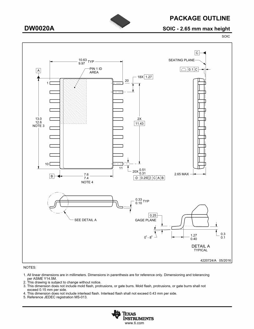
PACKAGE OUTLINE
C
TYP10.639.97
2.65 MAX
18X 1.27
20X 0.510.31
2X11.43
TYP0.330.10
0 - 80.30.1
0.25GAGE PLANE
1.270.40
A
NOTE 3
13.012.6
B 7.67.4
4220724/A 05/2016
SOIC - 2.65 mm max heightDW0020ASOIC
NOTES: 1. All linear dimensions are in millimeters. Dimensions in parenthesis are for reference only. Dimensioning and tolerancing per ASME Y14.5M. 2. This drawing is subject to change without notice. 3. This dimension does not include mold flash, protrusions, or gate burrs. Mold flash, protrusions, or gate burrs shall not exceed 0.15 mm per side. 4. This dimension does not include interlead flash. Interlead flash shall not exceed 0.43 mm per side.5. Reference JEDEC registration MS-013.
120
0.25 C A B
1110
PIN 1 IDAREA
NOTE 4
SEATING PLANE
0.1 C
SEE DETAIL A
DETAIL ATYPICAL
SCALE 1.200
www.ti.com
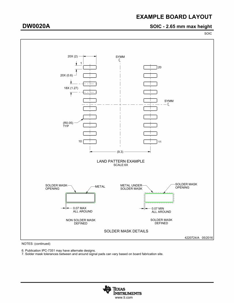
EXAMPLE BOARD LAYOUT
(9.3)
0.07 MAXALL AROUND
0.07 MINALL AROUND
20X (2)
20X (0.6)
18X (1.27)
(R )TYP
0.05
4220724/A 05/2016
SOIC - 2.65 mm max heightDW0020ASOIC
SYMM
SYMM
LAND PATTERN EXAMPLESCALE:6X
1
10 11
20
NOTES: (continued) 6. Publication IPC-7351 may have alternate designs. 7. Solder mask tolerances between and around signal pads can vary based on board fabrication site.
METALSOLDER MASKOPENING
NON SOLDER MASKDEFINED
SOLDER MASK DETAILS
SOLDER MASKOPENING
METAL UNDERSOLDER MASK
SOLDER MASKDEFINED
www.ti.com
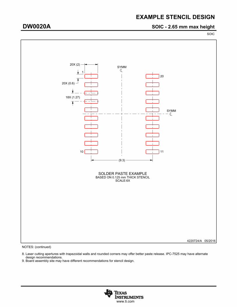
EXAMPLE STENCIL DESIGN
(9.3)
18X (1.27)
20X (0.6)
20X (2)
4220724/A 05/2016
SOIC - 2.65 mm max heightDW0020ASOIC
NOTES: (continued) 8. Laser cutting apertures with trapezoidal walls and rounded corners may offer better paste release. IPC-7525 may have alternate design recommendations. 9. Board assembly site may have different recommendations for stencil design.
SYMM
SYMM
1
10 11
20
SOLDER PASTE EXAMPLEBASED ON 0.125 mm THICK STENCIL
SCALE:6X

IMPORTANT NOTICE
Texas Instruments Incorporated (TI) reserves the right to make corrections, enhancements, improvements and other changes to itssemiconductor products and services per JESD46, latest issue, and to discontinue any product or service per JESD48, latest issue. Buyersshould obtain the latest relevant information before placing orders and should verify that such information is current and complete.TI’s published terms of sale for semiconductor products (http://www.ti.com/sc/docs/stdterms.htm) apply to the sale of packaged integratedcircuit products that TI has qualified and released to market. Additional terms may apply to the use or sale of other types of TI products andservices.Reproduction of significant portions of TI information in TI data sheets is permissible only if reproduction is without alteration and isaccompanied by all associated warranties, conditions, limitations, and notices. TI is not responsible or liable for such reproduceddocumentation. Information of third parties may be subject to additional restrictions. Resale of TI products or services with statementsdifferent from or beyond the parameters stated by TI for that product or service voids all express and any implied warranties for theassociated TI product or service and is an unfair and deceptive business practice. TI is not responsible or liable for any such statements.Buyers and others who are developing systems that incorporate TI products (collectively, “Designers”) understand and agree that Designersremain responsible for using their independent analysis, evaluation and judgment in designing their applications and that Designers havefull and exclusive responsibility to assure the safety of Designers' applications and compliance of their applications (and of all TI productsused in or for Designers’ applications) with all applicable regulations, laws and other applicable requirements. Designer represents that, withrespect to their applications, Designer has all the necessary expertise to create and implement safeguards that (1) anticipate dangerousconsequences of failures, (2) monitor failures and their consequences, and (3) lessen the likelihood of failures that might cause harm andtake appropriate actions. Designer agrees that prior to using or distributing any applications that include TI products, Designer willthoroughly test such applications and the functionality of such TI products as used in such applications.TI’s provision of technical, application or other design advice, quality characterization, reliability data or other services or information,including, but not limited to, reference designs and materials relating to evaluation modules, (collectively, “TI Resources”) are intended toassist designers who are developing applications that incorporate TI products; by downloading, accessing or using TI Resources in anyway, Designer (individually or, if Designer is acting on behalf of a company, Designer’s company) agrees to use any particular TI Resourcesolely for this purpose and subject to the terms of this Notice.TI’s provision of TI Resources does not expand or otherwise alter TI’s applicable published warranties or warranty disclaimers for TIproducts, and no additional obligations or liabilities arise from TI providing such TI Resources. TI reserves the right to make corrections,enhancements, improvements and other changes to its TI Resources. TI has not conducted any testing other than that specificallydescribed in the published documentation for a particular TI Resource.Designer is authorized to use, copy and modify any individual TI Resource only in connection with the development of applications thatinclude the TI product(s) identified in such TI Resource. NO OTHER LICENSE, EXPRESS OR IMPLIED, BY ESTOPPEL OR OTHERWISETO ANY OTHER TI INTELLECTUAL PROPERTY RIGHT, AND NO LICENSE TO ANY TECHNOLOGY OR INTELLECTUAL PROPERTYRIGHT OF TI OR ANY THIRD PARTY IS GRANTED HEREIN, including but not limited to any patent right, copyright, mask work right, orother intellectual property right relating to any combination, machine, or process in which TI products or services are used. Informationregarding or referencing third-party products or services does not constitute a license to use such products or services, or a warranty orendorsement thereof. Use of TI Resources may require a license from a third party under the patents or other intellectual property of thethird party, or a license from TI under the patents or other intellectual property of TI.TI RESOURCES ARE PROVIDED “AS IS” AND WITH ALL FAULTS. TI DISCLAIMS ALL OTHER WARRANTIES ORREPRESENTATIONS, EXPRESS OR IMPLIED, REGARDING RESOURCES OR USE THEREOF, INCLUDING BUT NOT LIMITED TOACCURACY OR COMPLETENESS, TITLE, ANY EPIDEMIC FAILURE WARRANTY AND ANY IMPLIED WARRANTIES OFMERCHANTABILITY, FITNESS FOR A PARTICULAR PURPOSE, AND NON-INFRINGEMENT OF ANY THIRD PARTY INTELLECTUALPROPERTY RIGHTS. TI SHALL NOT BE LIABLE FOR AND SHALL NOT DEFEND OR INDEMNIFY DESIGNER AGAINST ANY CLAIM,INCLUDING BUT NOT LIMITED TO ANY INFRINGEMENT CLAIM THAT RELATES TO OR IS BASED ON ANY COMBINATION OFPRODUCTS EVEN IF DESCRIBED IN TI RESOURCES OR OTHERWISE. IN NO EVENT SHALL TI BE LIABLE FOR ANY ACTUAL,DIRECT, SPECIAL, COLLATERAL, INDIRECT, PUNITIVE, INCIDENTAL, CONSEQUENTIAL OR EXEMPLARY DAMAGES INCONNECTION WITH OR ARISING OUT OF TI RESOURCES OR USE THEREOF, AND REGARDLESS OF WHETHER TI HAS BEENADVISED OF THE POSSIBILITY OF SUCH DAMAGES.Unless TI has explicitly designated an individual product as meeting the requirements of a particular industry standard (e.g., ISO/TS 16949and ISO 26262), TI is not responsible for any failure to meet such industry standard requirements.Where TI specifically promotes products as facilitating functional safety or as compliant with industry functional safety standards, suchproducts are intended to help enable customers to design and create their own applications that meet applicable functional safety standardsand requirements. Using products in an application does not by itself establish any safety features in the application. Designers mustensure compliance with safety-related requirements and standards applicable to their applications. Designer may not use any TI products inlife-critical medical equipment unless authorized officers of the parties have executed a special contract specifically governing such use.Life-critical medical equipment is medical equipment where failure of such equipment would cause serious bodily injury or death (e.g., lifesupport, pacemakers, defibrillators, heart pumps, neurostimulators, and implantables). Such equipment includes, without limitation, allmedical devices identified by the U.S. Food and Drug Administration as Class III devices and equivalent classifications outside the U.S.TI may expressly designate certain products as completing a particular qualification (e.g., Q100, Military Grade, or Enhanced Product).Designers agree that it has the necessary expertise to select the product with the appropriate qualification designation for their applicationsand that proper product selection is at Designers’ own risk. Designers are solely responsible for compliance with all legal and regulatoryrequirements in connection with such selection.Designer will fully indemnify TI and its representatives against any damages, costs, losses, and/or liabilities arising out of Designer’s non-compliance with the terms and provisions of this Notice.
Mailing Address: Texas Instruments, Post Office Box 655303, Dallas, Texas 75265Copyright © 2017, Texas Instruments Incorporated