d04.16 enhanced demonstration platforms
TRANSCRIPT

ARTEMIS Call 2013, project 621429 EMC²
D4.16_PU - Enhanced Demonstration Platforms Page 1 of 40
Embedded multi-core systems for
mixed criticality applications
in dynamic and changeable real-time environments
Project Acronym:
EMC²
Grant agreement no: 621429
Deliverable no. and title D4.16_PU – Enhanced Demonstration Platforms
Work package WP4 MultiCore Hardware Architectures and Concepts
Task / Use Case
Subtasks involved
Lead contractor Infineon Technologies AG
Dr. Werner Weber, mailto:[email protected]
Editor responsible Sundance – Mr. Flemming Christensen, [email protected]
Version number v1.0
Date 23th
November 2015
Status Converted from official D4.16 of 30.10.2015
Dissemination level Public (PU)
Copyright: EMC2 Project Consortium, 2015

ARTEMIS Call 2013, project 621429 EMC²
D4.16_PU - Enhanced Demonstration Platforms Page 2 of 40
Authors ID# Name Author name Chapter Title
04D UTIA Jiri Kadlec,
Zdenek Pohl
Chapter 1
Introduction
01V
TUBS
RUBS
TUDO
Rolf Meyer,
Jan Wagner,
Lilian Tadros
Chapter 2
EMC2 SoC-Rocket
Virtual Platform Framework
04D UTIA Jiri Kadlec,
Zdenek Pohl,
Lukas Kohout
Chapter 3
Asymmetric Multiprocessing on
Xilinx Zynq and HDMI I/O
15O SevenS Javier Diaz,
Benoit Rat,
José Luis Gutiérrez
Chapter 4
Dependable and high accuracy time transfer
for distributed control applications, using
Xilinx Zynq.
02A
01L
01A
02 F
AVL/GRZ
EB
IFAG
VIF
Eric Armengaud,
Peter Priller
Alexander Mattausch
Werner Weber
Allan Tengg
Chapter 5
Automotive domain:
Network technologies and connection to
testbed
02D
02E
TTT
TUW
Andreas Eckel
Haris Isakovic
Chapter 6
Multi-processor System-on-Chip Architecture
for Cross-domain applications on Altera SoC
02C IFAT Thomas Herndl,
Norbert Druml
Chapter 7
Automotive Time-of-Flight Demonstrator
18M ENSILICA David Wheeler Chapter 8
Fine Grain Partially Reconfigurable Array of
Processors on Xilinx Zynq with Linux support
18D Sundance Emilie Wheatley Chapter 9
HDMI-in video processing to HDMI-out
controlled by Ethernet port on Xilinx Zynq
11K POLITO Massimo Violante Chapter 10
Demonstrator platform for multicore avionic
systems on Zynq
04D UITA Jiri Kadlec Chapter 11 Conclusion
ARTEMIS Call 2013, project 621429 EMC²
D4.16_PU - Enhanced Demonstration Platforms Page 3 of 40
Document History
Version Date Author name Reason
v0.9 16/11/15 Flemming Christensen
(Sundance)
Edit of D4.16
v1.0 23/11/15 Flemming Christensen
(Sundance)
Corrections, as requested by Partners.

ARTEMIS Call 2013, project 621429 EMC²
D4.16_PU - Enhanced Demonstration Platforms Page 4 of 40
Summary
This deliverable is presenting enhanced demonstration platforms including basic innovative techniques in
form of demonstrators prepared by WP4 partners in the EMC2 project. It describes following
demonstrators:
EMC2 SoCRocket - transaction-level modelling framework for space applications
Asymmetric Multiprocessing on Zynq and HDMI I/O demonstrator
Dependable and high accuracy time transfer for distributed control applications
Automotive domain: network technologies and connection to testbed
Multi-processor system-on-chip architecture for cross-domain applications
Automotive time-of-flight demonstrator
Fine grain partially reconfigurable array of processors on Zynq with Linux support
HDMI-In video processing to HDMI-Out controlled by Ethernet port on Zynq
Demonstrator platform for multicore avionic systems on Zynq
WP4 tasks T4.2 T4.3 and T4.4 cooperating with T4.6 in the D4.16 demonstrator’s development
This enhanced demonstration platforms including basic innovative techniques milestone present the status
of developments within the WP4 package in the middle of the EMC2 project. Demonstrators form
concrete base for the collaboration and developments in the EMC2 project.
T4.2
T4.3
T4.4 T4.6

ARTEMIS Call 2013, project 621429 EMC²
D4.16_PU - Enhanced Demonstration Platforms Page 5 of 40
Table of contents
Summary ..... ............................................................................................................................................................ 4
1. Introduction .............................................................................................................................................................. 7
2. EMC2 SoC-Rocket –Virtual Platform Framework ................................................................................................... 8
2.1 Overview ......................................................................................................................................................... 8
2.2 Infrastructure ................................................................................................................................................... 9
2.3 Conditions for use, downloads ...................................................................................................................... 10
3. Asymmetric Multiprocessing on ZYNQ and HDMI I/O demonstrator .................................................................. 11
3.1 Key features of the AMP demonstrator with EdkDSP accelerators .............................................................. 11
3.2 Resources used by the designs ...................................................................................................................... 13
3.2.1 Asymmetric multiprocessing and use of external DDR3 memory ................................................... 13 3.2.2 Re-programmability of EdkDSP accelerators ................................................................................... 13 3.2.3 Debug of the AMP system with EdkDSP accelerators in the evaluation package ............................ 14
3.3 Asymmetric Multiprocessing Demo ............................................................................................................. 15
3.4 Performance of ARM A9 NEON and EdkDSP accelerator .......................................................................... 15
3.5 Asymmetric Multiprocessing Demo with single EdkDSP accelerator with In-circuit Logic Analyser ........ 16
3.5.1 ILA debug ports of the (8xSIMD) EdkDSP accelerator. .................................................................. 16
3.6 Conditions for use, downloads ...................................................................................................................... 18
3.7 Key features of the HDMI demos ................................................................................................................. 19
3.7.1 HDMIO .. .......................................................................................................................................... 19 3.7.2 IM-HDMIO ...................................................................................................................................... 19 3.7.3 IM-HDMII-HDMIO ......................................................................................................................... 19 3.7.4 IM-VITA-HDMIO ............................................................................................................................ 19
4. Dependable and high accuracy time transfer for distributed control applications ................................................. 20
4.1 WR demonstrator features & elements ......................................................................................................... 20
4.1.1 Time & Frequency Transfer Robustness .......................................................................................... 21
4.2 Conditions for use, downloads ...................................................................................................................... 22
5. Automotive domain: Network technologies and connection to testbed ................................................................. 23
5.1 Description, parameters, photos, diagrams ................................................................................................... 24
5.2 Conditions for use, downloads ...................................................................................................................... 25
6. Time-triggered Multi-processor System-on-Chip Architecture for Cross-domain applications ............................ 26
6.1 Legacy MPSoC ............................................................................................................................................. 26
6.2 EMC2 TTNoC Many-core Architecture on Altera Arria V ........................................................................... 26
6.3 Conditions for use, downloads ...................................................................................................................... 28
7. Enhanced Automotive Time-of-Flight Demonstrator ............................................................................................ 29
7.1 Introduction ................................................................................................................................................... 29
7.2 Description, parameters, photos, diagrams ................................................................................................... 29
7.3 Conditions for use, downloads ...................................................................................................................... 30
8. Fine Grain Partially Reconfigurable Array of Processors on Zynq with Linux reprogramming support............... 31
8.1 Description, parameters, photos, diagrams ................................................................................................... 31
8.2 Conditions for use, downloads ...................................................................................................................... 31
9. HDMI-in video processing to HDMI-out controlled by Ethernet port ................................................................... 32

ARTEMIS Call 2013, project 621429 EMC²
D4.16_PU - Enhanced Demonstration Platforms Page 6 of 40
9.1 Description, photos, diagrams ....................................................................................................................... 32
9.2 Conditions for use, downloads ...................................................................................................................... 34
10. Demonstrator platform for multicore avionic systems ........................................................................................... 36
10.1 Description of the architecture ...................................................................................................................... 36
10.2 Description of the demonstrator .................................................................................................................... 38
11. Conclusions ............................................................................................................................................................ 39
12. References .............................................................................................................................................................. 40
List of figures Figure 1: SoC-Rocket Models ....................................................................................................................................... 8 Figure 2: SoC-Rocket Structure ................................................................................................................................... 9 Figure 3: Model design ............................................................................................................................................. 10 Figure 4: Prototype of the EMC
2-DP Platform w. Imageon FMC board for HDMI I/O and HD video sensor. ........ 12
Figure 5: AMP design on ZYNQ, ARM A9, MicroBlaze and 1x (8xSIMD) EdkDSP, with FP division ..................... 13 Figure 6: AMP designs on ZYNQ, ARM A9, MicroBlaze and 4x (8xSIMD) EdkDSP, with FP division .................... 13 Figure 7: Simplified architecture of AMP with four EdkDSP accelerators ................................................................ 14 Figure 8: Measured performance in MFLOP/s for FIR filter computation ................................................................ 15 Figure 9: Measured performance in MFLOP/s for LMS filter computation .............................................................. 15 Figure 10: AMP design with Vivado In-Circuit Logic Analyzer on Zynq................................................................... 16 Figure 11: Vivado Lab Edition 2015.2 ILA display of the FIR filter computation ..................................................... 17 Figure 12: Vivado Lab Edition 2015.2 ILA display of adaptive LMS filter computation ........................................... 18 Figure 13: WR-Switch, WR-ZEN (Zynq architecture) and WR-LEN (node based on Artix FPGA). .......................... 21 Figure 14: Heterogeneous Time & Frequency Distribution network using White-Rabbit (PTP) and IRIG-B ........... 22 Figure 15: Overview of Blocks ................................................................................................................................... 24 Figure 16: Overview of V&V aspect of the use case .................................................................................................. 24 Figure 17: Overview of V&V aspect of the use case .................................................................................................. 25 Figure 18: Vehicle Test Bed Figure 19: Engine Test Bed ........................................................................ 25 Figure 20 Arria V SoC Development Board and Block Diagram of the Architecture ................................................ 27 Figure 21: EMC
2 TTNoC MPSoC Architecture ......................................................................................................... 28
Figure 22: Concept of the enhanced automotive Time-of-Flight demonstrator ......................................................... 29 Figure 23: Data path of the hardware accelerated Time-of-Flight processing platform ........................................... 30 Figure 24: Photo of demonstrator carrier board and module .................................................................................... 31 Figure 25: Screen-shot of control console .................................................................................................................. 33 Figure 26: Diagram describing the Sundance demonstrator ..................................................................................... 34 Figure 27: Common WP4 demonstration at the EMC
2 conference Wienna 30.9.2015 .............................................. 35
Figure 28: Sundance EMC2-DP board with the HDM-IN HDMI-OUT application demo ......................................... 35
Figure 29: Proposed Architecture .............................................................................................................................. 36 Figure 30: Messages exchanged among architecture components ............................................................................ 37

ARTEMIS Call 2013, project 621429 EMC²
D4.16_PU - Enhanced Demonstration Platforms Page 7 of 40
1. Introduction
WP4 of the EMC2 project deals with new multi-core hardware architectures and concepts.
This deliverable is presenting eight early demonstrators provided by EMC2 WP4 partners at month M8 of
the project. These contributions form concrete base for the collaboration and future developments in the
EMC2 project.
Each contribution is describing an overview of the early demonstrator and it is pointing to detailed
information and documentation provided by individual partners.
We have selected this format to motivate the bottom up cooperation of partners within WP4, with other
technical work packages, and cooperation together with the Living Labs partners of the EMC2 project.
Workpackage 4 is focusing on four technology lanes:
(1) Heterogeneous Multiprocessor SoC architectures
(2) Dynamic reconfiguration on HW accelerators and reconfigurable logic
(3) Networking
(4) Virtualization and verification technologies
This deliverable describes wp4 demonstrators for Technology Lanes (1), (2), (3) and (4).
Contributions to these technology lines are indicated in each chapter. The concrete technical topics are
also visualized on the symbolic „architecture“ by a bullet.

ARTEMIS Call 2013, project 621429 EMC²
D4.16_PU - Enhanced Demonstration Platforms Page 8 of 40
2. EMC2 SoC-Rocket –Virtual Platform Framework
Technology lanes covered:
Heterogeneous Multiprocessor SoC architectures Dynamic reconfiguration on HW accelerators and
reconfigurable logic
Networking
Virtualization and verification technologies
Increasingly large portions of electronic systems are being implemented in software and its development
cost starts dominating the overall system's cost. Software is also becoming the critical part of the
development schedule, mainly because deploying and testing it on the real target hardware is
complicated.
Transaction Level Models (TLMs) are used to describe both, timing and functionality, of system
components and their communication interfaces at a high abstraction level. Embedded in a virtual
platform, these models are sufficiently accurate to allow early software development and verification in a
realistic environment and functional verification of the modeled hardware. The capability of early design-
space exploration is therefore a vital building block of full hardware/software co-design.
To achieve these goals, we designed the SoC-Rocket Framework. Written in SystemC/TLM, it is fitted to
serve the industry's special needs. It already builds the foundation of space-domain ESL design. We tied
together the following features to enable the construction of virtual platforms for various applications:
Models - All models are designed to simulate their corresponding counterparts from the
COBHAM/Aeroflex Gaisler GRLib (also available under GPL)
Platform Generator - Easy configuration via GUI or from the command line
Automation Tools - To run big batches of design-space explorations
Infrastructure - Reusable components for building new components at ease
Build System - Extended build system for compiling models, platforms, target software, RTL co-
simulations, and regression tests
2.1 Overview
Our activities in this project aim towards
implementation and validation of an
efficient methodology allowing software to
be developed before the final hardware is
ready. We have therefore developed a
design flow for the implementation of
virtual platforms (VP) based on TLM in
SystemC.
To support the developed design flow it was
mandatory to stock it up with basic models
and a supportive foundation. This allows the
users to be faster through reuse of already
existing components. It also gives model developers a starting point to derive their models from.
The outcome of this project is now bundled as a library, which we call the SoC-Rocket – Virtual Platform
Framework.
Hence the free availability of the COBHAM/Aeroflex Gaisler GRLib Components we designed our
Models to behave alike, therefore all models found in the SoC-Rocket Framework have a corresponding
AHB2SW
AHBCTRL
MCTRL
SR
AM
SD
RA
M
IO
PR
OM
SoCWire
GPTimer
SpaceWire
IRQMP AHB2APB
AHBOUT
AHBIN
AHBMEM
APBUART AHBProf
AHB
Display
LEON ISS
mmu-cache i/d cache
mmu localrams
ARM
Cortex-A9
predictable mmu-cache
i/d cache mmu
AHB
Camera
Ethernet
Network
Interface
NoC
Figure 1: SoC-Rocket Models

ARTEMIS Call 2013, project 621429 EMC²
D4.16_PU - Enhanced Demonstration Platforms Page 9 of 40
RTL component in the GRLib. Platforms constructed and tested in our Framework can easily be migrated
to the GRLib and simulated and synthesized at RTL level.
2.2 Infrastructure
As foundation (orange) for our library we
selected a series of appropriate infrastruc-
ture components and built a layer of
abstraction upon them (red).
We contribute a modeling kit for fast TL
signal communication to the foundation.
Throughout the library the SignalKit is
used to model interrupt lines, reset and
snooping. As well as an extended logging
mechanisms, sr_report, especially useful
for simulation observation and output. It
can be configured in seven levels that can
be set globally or for a single module. A model registry (sr_registry) can be used to dynamically
instantiate models and prevent recompilation. And last but not least we extended the gs_params with meta
parameters to allow easy handling of meta information in addition to generics, registers and other non
memory mapped data.
(Pred. Het. MP)
(Ethernet)
(NoC)
(LEON4 Terma)
GreenSoCs
GreenSockets Carbon
AMBAKit Accellera CCI
GreenControl
c3e
SignalKit
Base AHBMaster AHBSlave APBSlave …
Models
IEEE
SystemC IEEE
TLM Cadence
scireg GreenSoCs
GreenReg ESA
TrapGen
(Computer Vision)
Waf
Build System
Virtual
Platforms
Deps
Mgr. (Space Domain)
Repo
Mgr.
sr_param sr_report sr_register sr_registry …
(core)
Model Libraries
Figure 2: SoC-Rocket Structure

ARTEMIS Call 2013, project 621429 EMC²
D4.16_PU - Enhanced Demonstration Platforms Page 10 of 40
One of the main purposes of the
library is to leverage the development
of new components and to test them
on system level before going to RTL.
To make this as easy as possible we
provide a set of library base classes
encapsulating the communication and
the storage part of the models. All
our models, except the AHBCTRL
are structured this way.
On the left side of the previous figure
you see a typical AHB master
component. The model is a C++ class
which inherits a register file and an APB slave socket from class APBSlave and an AHB master socket
from class AHBMaster. The user ought to fill out the behavior, which is the green part in the middle. For
access to the sockets there is a simple read/write API. The register file can be equipped with callbacks for
read and write operations to any register or bit field. In AT mode the port interface triggers a response
function in the behavior, as soon data is available at the socket.
Slaves are structured in a similar ways. Only this time the implementing module inherits from class
AHBSlave giving it an AHB TLM target socket. For any request the slave interface triggers a callback in
the behavior. All details of the state machines in the front-end are hidden.
2.3 Conditions for use, downloads
In the last 20 months TU Braunschweig (c3e) was extending, debugging and stabilizing the framework as
a preparation to publish it to the project consortium with legwork and support by TU Dortmund.
Furthermore, confidential components were removed and replaced to smooth out some legal issues.
In addition to that the following changes are made from D4.15:
Deep introspection via sr_report and USI
NoC and Network interface models (in separated repository)
Introducing ARM Cortex-A9 Processor
Introducing Predictable Caches for LEON and ARM
GREth model (in separated repository)
GreenReg replaced by sr_register
GreenControl gs_param were replaced by sr_params
LEON3 CPU Fixes for better interrupt handling
AHBCtrl speed up, APBUart improvements
And many more (see commit log)
You can find our code and documentation at http://socrocket.github.io/
Download the core platform for EMC2 partners from https://github.com/socrocket/core. The code is
available under AGPL. Additional repositories or license schemes are available. Please contact us:
Contact:
TU Braunschweig, c3e, Rolf Meyer, [email protected], +49 531 391 2378
TU Braunschweig, c3e, Jan Wagner, [email protected], +49 531 391 2387
TU Dortmund, Lilian Tadros, [email protected], +49 231 755-4670
Figure 3: Model design

ARTEMIS Call 2013, project 621429 EMC²
D4.16_PU - Enhanced Demonstration Platforms Page 11 of 40
3. Asymmetric Multiprocessing on ZYNQ and HDMI I/O demonstrator
Technology lanes covered:
Heterogeneous Multiprocessor SoC architectures
Dynamic reconfiguration on HW accelerators and reconfigurable logic
Networking
Virtualization and verification technologies
This section describes two demonstrators on the Trenz electronic TE0720-02-2I System on Module
(SOM) [2] and the TE0701-05 carrier board [3]. See Figure 4.
The asymmetric multiprocessing demonstrator design is integrating on ZYNQ one ARM Cortex A9
processor with vector floating point accelerator NEON, one MicroBlaze processor and four run-time
reprogrammable (8xSIMD) EdkDSP floating point accelerators in the programmable logic of ZYNQ [4].
The HDMI I/O describes four different designs demonstrating the HDMI output HDMI input [14] and
Vita 2000 color video sensor input [16], in full HD resolution (1920x1080p60).
All designs are precompiled in Xilinx Vivado 2015.2 [5] and aim to support the Software Defined System
on Chip tool chain SDSoC 2015.2 [20] introduced in summer 2015 by Xilinx. All designs aim to be in the
future portable to the EMC2-DP platform [15] developed by Sundance. See Chapter 9.
3.1 Key features of the AMP demonstrator with EdkDSP accelerators
This application note describes the asymmetric multiprocessing design (AMP) based on the Xilinx
application note XAPP1093 [1]. The AMP design has been ported from the ISE 14.5 design flow to the
Xilinx Vivado 2015.2 and SDK 2015.2 design flow. The ARM Cortex A9 processor [4] works together
with the MicroBlaze processor, sharing the terminal and block ram. Both processors execute program
from the same external DDR3 memory. The MicroBlaze processor is controlling 4 EdkDSP floating-point
accelerators. Each accelerator is organised as 8xSIMD reconfigurable data path, controlled by the
PicoBlaze6 controller [7].
This demonstrator and related evaluation package is provided by UTIA for the Trenz electronic TE0720-
02-2I System on Module [2] and the TE0701-05 carrier board [3]. These features are demonstrated:
Implementation of adaptive acoustic noise cancellation on 1 of 4 accelerators is computing the
recursive adaptive LMS algorithm for identification of regression filter with 2000 coefficients in
single precision floating point arithmetic with sustained performance
o 777 MFLOP/s on single 125 MHz (8xSIMD) EdkDSP accelerator
o 338 MFLOP/s on single 666 MHz ARM Cortex A9 (with the vector NEON unit)
o 160 MFLOP/s on single 666 MHz ARM Cortex A9 (with the 32bit floating point unit)
o 10 MFLOP/s on single 125 MHz MicroBlaze processor (with the 32bit floating point unit)
The EdkDSP accelerators can be reprogrammed by firmware. The programming is possible in C with
the use of the UTIA EDKDSP C compiler. Accelerators can be programmed with two firmware
programs. Designs can swap in the real time the firmware in only few clock cycles in the runtime.
The floating-point applications are scheduled inside of the 8x SIMD EdkDSP accelerator by the
Xilinx PicoBlaze6 processor [7]. Each firmware program has maximal size of 4096 (18 bit wide
words). The alternative firmware can be downloaded to the EdkDSP accelerators in parallel with the
execution of the current firmware. This is demonstrated by swap of the firmware for the FIR filter
room response to the firmware for adaptive LMS identification of the filter coefficients in the
acoustic noise cancellation demo.
The 8xSIMD EdkDSP accelerator is providing single-precision floating-point results bit-exact
identical to the reference software implementation running on MicroBlaze processor with the Xilinx
floating point unit.

ARTEMIS Call 2013, project 621429 EMC²
D4.16_PU - Enhanced Demonstration Platforms Page 12 of 40
The 125 MHz 8xSIMD EdkDSP accelerator is 2,3x faster than the 666 MHz ARM Cortex A9 (with
NEON vector processing unit) 4,8x faster than the 666 MHz ARM Cortex A9 without code optimized
for NEON and 78x faster than 125 MHz MicroBlaze with HW floating point unit. These data are
measured for the presented case of the 2000 tap adaptive LMS filter.
The floating-point 2000 tap coefficients FIR filter (acoustics room model) is computed by single 125
MHz (8xSIMD) EdkDSP accelerator with the floating point performance 1234 MFLOP/s. The peak
performance of the single 125 MHz (8xSIMD) EdkDSP accelerator is 2 GFLOP/s.
The peak performance of four 125 MHz (8xSIMD) EdkDSP accelerators implemented in this demo
design is 8 GFLOP/s.
System-on-Module
TE0720-02-2I
(5cm x 4cm)
Figure 4: Prototype of the EMC
2-DP Platform w. Imageon FMC board for HDMI I/O and HD video sensor.
The EdkDSP accelerator IP core bce_fp12_1x8_0_axiw_v1_40 performs:
Vector floating point operations FPADD, FPSUB in 8 SIMD data paths.
Vector floating point MAC operations in 8 SMD data paths for length of the vector 1 up to 10. These
accelerators can be used in applications like floating point matrix multiplication with row and column
dimensions <= 10.
Floating-point vector-by-vector dot products performed in 8 SIMD data paths. It is optimized for
parallel computation of up to 8 FIR or LMS filters, each with size up to 255 coefficients. It is also
effective in case of floating-point matrix-by-matrix multiplications, where one of the dimensions is
large (in the range from 11 to 255).

ARTEMIS Call 2013, project 621429 EMC²
D4.16_PU - Enhanced Demonstration Platforms Page 13 of 40
Additional HW support of dot product. It is computed in 8 data paths with the HW supported wind-up
into single scalar result.
Support for single data path the pipelined vector floating point division. Accelerators is suitable for
applications like adaptive recursive (normalised) NLMS filters and the square root free versions of
adaptive RLS QRD filters and adaptive square root free RLS QRD LATTICE filters.
The system clock of ARM Cortex A9 is 666 MHz, MicroBlaze 125 MHz and EdkDSP accelerators
125 MHz.
The EdkDSP floating-point accelerators are reconfigurable during runtime by change of firmware.
Asymmetric multiprocessing of ARM Cortex A9 and MicroBlaze system with shared external DDR3.
AMP EdkDSP HW evaluation designs have been compiled in Xilinx VIVADO 2015.2 [5] with SW
projects for SDK 2015.2 [6]. Presented HW accelerators can results in better POWER per MFLOPS ratio
for certain class of DSP applications in comparison to the computation on standard CPUs with standard
HW floating point support. The AMP EdkDSP demonstrator includes source code of set of SW demos
prepared for easy import of projects and compilation in the Xilinx SDK 2015.2 [6].
3.2 Resources used by the designs
Figure 5 and Figure 6 present resources used by both designs.
7z020-1 fp32 fp32 fp32 fp32 fp32 Resources (complete PL) EdkDSP performance
EdkDSP
vector op.
Add
Mul Mac
Dot
Prod
S8
Prod
div
FF
%
Lut
%
Bram
no(of)
LMS
Mflop/s
FIR
Mflop/s
fp12_1x8_40 8x 8x 8x 1x 1x 10 21 48(140) 777 1234
Figure 5: AMP design on ZYNQ, ARM A9, MicroBlaze and 1x (8xSIMD) EdkDSP, with FP division
7z020-1 fp32 fp32 fp32 fp32 fp32 Resources (complete PL) EdkDSP performance
EdkDSP
vector op.
Add
Mul Mac
Dot
Prod
S8
Prod
div
FF
%
Lut
%
Bram
no(of)
LMS
Mflop/s
FIR
Mflop/s
(4x)
fp12_1x8_40
(4x)
8x
(4x)
8x
(4x)
8x
(4x)
1x
(4x)
1x 30 82 138(140) (4x)
777
(4x)
1234
Figure 6: AMP designs on ZYNQ, ARM A9, MicroBlaze and 4x (8xSIMD) EdkDSP, with FP division
3.2.1 Asymmetric multiprocessing and use of external DDR3 memory
Presented FPGA designs are running on the Trenz electronic TE0720-02-2I System on Module [2] and
the TE0701-05 carrier board [3]. See Figure 4. It is using the 1GB DDR3 memory with clock signal 533
MHz. The DDR3 is connected to Xilinx ZYNQ xc7z020-2I FPGA by 32 data path. The first ¾ of the
DDR3 are reserved for the ARM A9 processor. The last ¼ is used by the MicroBlaze processor with the
EdkDSP accelerators. The presented AMP demo is extending the Xilinx application note XAPP1093 [1]
solution from the Xilinx ISE/EDK 14.5 flow to the Xilinx Vivado 2015.2 design flow. See Figure 7 for
the architecture of the design.
3.2.2 Re-programmability of EdkDSP accelerators
Each of the four 125 MHz 8xSIMD EdkDSP floating-point accelerator subsystems contains one
reprogrammable Xilinx PicoBlaze6 8-bit processor and the floating point 8xSIMD DSP unit. The
performance of the accelerator is application specific. In this demo, a single 8xSIMD EdkDSP unit is
delivering sustained 1234 MFLOP/s in case of 2000 tap FIR filter computation and 777 MFLOP/s in case
of the adaptive 2000 tap LMS filter identification demo. The Xilinx PicoBlaze6 [7] controller has fixed
configuration with size of the program memory 4096 (18 bit wide) words, 64 Bytes scratch pad RAM
memory and the interrupt vector in the address 1023. Both PicoBlaze6 program memories are accessible
by the MicroBlaze processor via AXI-lite bus. The PicoBlaze6 controller can execute program from each
of these memories. The MicroBlaze application can write new firmware to the currently unused program

ARTEMIS Call 2013, project 621429 EMC²
D4.16_PU - Enhanced Demonstration Platforms Page 14 of 40
memory, while the EdkDSP accelerators and their PicoBlaze6 controllers are executing firmware from
second program memory.
3.2.3 Debug of the AMP system with EdkDSP accelerators in the evaluation package
All EdkDSP accelerators can communicate with MicroBlaze program. The communication is using the
UTIA Worker Abstraction Layer (WAL) library API. This API is also used for support of writing of the
debug information from the worker to the MicroBlaze terminal. MicroBlaze is using the terminal of the
ARM A9 processing system, present in the ZYNQ processing system [4]. ARM A9 and MicroBlaze
communicate via the internal shared memory controller of the ZYNQ processing system [4]. See Figure
7.
Figure 7: Simplified architecture of AMP with four EdkDSP accelerators
ARM and MicroBlaze can be both debugged simultaneously from the SDK 2015.2 GDB debugger
integrated in the Xilinx SDK tool [6]. PicoBlaze6 controllers [7] can exchange data and text via the 8 bit
communication data paths and AXI-lite bus with the MicroBlaze processor. This path is used to

ARTEMIS Call 2013, project 621429 EMC²
D4.16_PU - Enhanced Demonstration Platforms Page 15 of 40
communicate parameters to the accelerators and to get messages or reports from accelerators for
debugging.
Floating-point data are accessed by the MicroBlaze processor via the dual ported block memories of
accelerators. The MicroBlaze sides of the dual-ported accelerator memories are all mapped into the
MicroBlaze memory space. The MicroBlaze processor can copy data from these dual ported memories to
its global DDR3 workspace and display floating point data in the debugger.
The computation in the (8xSIMD) EdkDSP units can overlap with communication with the DDR3. It is
performed by UTIA libwal.a API provided as MicroBlaze library and it is supported by MicroBlaze data
and program cache. A Ping-Pong swap of memory banks is used. The 8xSIMD EdkDSP firmware
scheduling the parallel (8xSIMD) computation in some banks of accelerator memories. The MicroBlaze
program is communicating (sequentially) to/from DDR3 in another set of banks of the dual-ported
accelerator memories. This process can be stopped, inspected and debugged by the MicroBlaze debugger
from the SDK debugger [6] in the synchronization functions defined in the UTIA libwal.a API.
3.3 Asymmetric Multiprocessing Demo
“amp_cpu_1x8_all” project in the “Project Explorer” window of the SDK 2015.2 [6] is used to
program ARM A9 part of the AMP demo.
“edkdsp_fp12_4x8_all” project is used to program the MicroBlaze core and the four EdkDSP
accelerators of the AMP demo.
“edkdsp” project contains libwal.a library for the MicroBlaze processor.
“edkdsp_cc” directory contains C source code for the PicoBlaze6 controller firmware and UTIA
EDKDSP C compiler binary for compilations of C and ASM code [7] for the PicoBlaze6
controller of the EdkDSP accelerators.
The UTIA EDKDSP C compiler can be executed in Win 7 64 bit under the VMware Workstation
12 Player [19] running in the preconfigured 32bit Linux Ubuntu image (provided by UTIA for
free) the 32 bit compiler binary application (provided by UTIA for free).
3.4 Performance of ARM A9 NEON and EdkDSP accelerator
The performance of processors and accelerators is dependent on the optimisation level of C compiler for
ARM and C compiler for MicroBlaze. Lines labled FIR ARM (see Figure 8 and Figure 9) document how
the ARM performance improves with the Compiler optimization level. Additional substantial
improvement can be reached only with manual transformation of the C source code for ARM A9
processor.
FIR MFLOP/s -O0 -O1 -O2 -O3
FIR ARM (666 MHz) 36 105 120 152
FIR ARM NEON (666 MHz) 56 351 342 466
FIR MB EdkDSP (125 MHz) 1234 1234 1234 1234
Figure 8: Measured performance in MFLOP/s for FIR filter computation
LMS MFLOP/s -O0 -O1 -O2 -O3
LMS ARM (666 MHz) 42 115 137 150
LMS ARM NEON (666 MHz) 49 284 277 352
LMS MB EdkDSP (125 MHz) 777 777 777 777
LMS MB (125 MHz) 3 7 10 10
Figure 9: Measured performance in MFLOP/s for LMS filter computation

ARTEMIS Call 2013, project 621429 EMC²
D4.16_PU - Enhanced Demonstration Platforms Page 16 of 40
This is visible in the lines FIR ARM NEON and LMS ARM NEON. The corresponding functions have
been reorganized to group together parallel computation of 4 floating point MAC operations in parallel.
This resulted in better use of the vector capabilities of the NEON unit.
The EdkDSP (8xSIMD) accelerator works with hand optimized code for the FIR and the LMS filter. The
optimization levels of the MicroBlaze C compiler have impact on the MicroBlaze processor performance
and only minimal influence on performance of the EdkDSP accelerators.
3.5 Asymmetric Multiprocessing Demo with single EdkDSP accelerator with In-
circuit Logic Analyser
The evaluation design with ARM A9 [4] processor and MicroBlaze processor with single (8xSIMD)
EdkDSP can be extended by the Vivado In-Circuit Logic Analyzer (ILA). It is part of the free Vivado Lab
Edition 2015.2 [21].
The implemented precompiled In-Circuit Logic Analyzer (ILA) can store 32k samples of all output
signals of the (8xSIMD) EdkDSP Accelerator labeled for the debug.
7z020-1 fp32 fp32 fp32 fp32 fp32 Resources (complete PL) EdkDSP performance
EdkDSP
vector op.
Add
Mul Mac
Dot
Prod
S8
Prod
div
FF
%
Lut
%
Bram
no(of)
LMS
Mflop/s
FIR
Mflop/s
fp12_1x8_40 8x 8x 8x 1x 1x 16 37 114(140) 777 1234
Figure 10: AMP design with Vivado In-Circuit Logic Analyzer on Zynq
Debug ports provide visibility of the vector (8xSIMD) EdkDSP accelerator. Debug probes help to trace
the integer addresses and the vector operation schedules. Floating-point data are not displayed. These data
can be better analyzed in the MicroBlaze debugger [4]. MicroBlaze programs can access all dual-ported
memories of the of the (8xSIMD) EdkDSP accelerator and copy these data to user-defined arrays declared
in the DDR3 in the user workspace of the MicroBlaze C application for debug in SDK 2015.2 debugger
[6].
3.5.1 ILA debug ports of the (8xSIMD) EdkDSP accelerator.
bce_atoa[0:9] Memory A address (addressing 1024 32 bit floating point values)
bce_atob[0:9] Memory B address (addressing 1024 32 bit floating point values)
bce_atoz[0:9] Memory Z address (addressing 1024 32 bit floating point values)
bce_done[0:7] Vector operation in progress or finished
bce_led4b[0:3] 4bit output, intended for led signalling. Unconnected in the design.
bce_mode[0:3] Mode of communication protocol PicoBlaze6 - MicroBlaze
bce_op[0:7] Vector operation to be performed.
bce_port[0:7] Data on external port.
bce_port_id[0:7] External port address. Address space [0x0 ... 0x1F] are reserved for
internal construction of the WLIW instruction to the 8xSIMD vector
processing unit of the EdkDSP. Address space [0x20 ... 0xFF]
can be used by the user.
bce_port_wr Write strobe related to writing of 8bit data to the external port address
bce_r_pb Reset of the PicoBlaze6
bce_we Write strobe related to writing of a WLIW instruction to the 8xSIMD
vector processing unit of the EdkDSP.
These signals can be all used for real-time analysis of the computation inside of the 8xSIMD vector-
processing unit of the EdkDSP. This helps with the debug of the coordination of the PicoBlaze6 firmware
code, the vector-processing unit together with MicroBlaze code.

ARTEMIS Call 2013, project 621429 EMC²
D4.16_PU - Enhanced Demonstration Platforms Page 17 of 40
The ILA triggering combination of probe signals can be initiated and modified from the EdkDSP
firmware running on the PicoBlaze6 controller. This firmware can be modified SDK 2015.2 editor and
recompiled by the UTIA EDKDSP C compiler running in [19].
Selected markers indicate single elementary step of the FIR filter. See Figure 11. It takes 308 clock cycles
(125 MHz = 8ns clock period) to compute the vector product of two floating-point vectors (coefficients
and data), both with length 248*8=1984 elements and to update the data vector (circular buffer). The ILA
HW support provides sufficient level of visibility and debug capabilities for the developer of the
(8xSIMD) EdkDSP firmware.
Figure 11: Vivado Lab Edition 2015.2 ILA display of the FIR filter computation
The red trigger is corresponding to the event. We can zoom in the data and define additional markers.
Selected markers to indicate single elementary step of the LMS filter. It takes 1154 clock cycles (125
MHz = 8ns clock period) to compute the vector product of two floating point vectors (coefficients and
data), both with length 248*8=1984 elements, update the data vector (circular buffer), compute the
prediction error and adapt the coefficients of the LMS filter.
The bce_op[0:7] debug signal is displayed in the analogue/hold mode and indicates the sequence of
vector operations issued by the PicoBlaze6 firmware, while implementing the single LMS step on single
(8xSIMD) EdkDSP vector unit.
The ARM code and the MicroBlaze code can be compiled with –O0, … , -O3 optimizations and executed
under both debuggers in combination with ILA triggering. The –O0 option provides lower performance
on ARM and MicroBlaze, but the corresponding code includes no transformations. This makes the
debugging of C code easier. This helps in debugging of the interactions of ARM A9, MicroBlaze and
EdkDSP accelerator. Complete exchanged blocks of floating point data can be inspected and verified in
the MicroBlaze GDB debugger in SDK 2015.2 [6].

ARTEMIS Call 2013, project 621429 EMC²
D4.16_PU - Enhanced Demonstration Platforms Page 18 of 40
Figure 12: Vivado Lab Edition 2015.2 ILA display of adaptive LMS filter computation
The EdkDSP accelerator code is deterministic and all operations can be emulated in the MicroBlaze C
code, including the exact sequence of all floating-point operations. The floating-point unit cores of the
MicroBlaze for the ADD and MULT provide bit-exact identical results to the floating-point units used in
the (8xSIMD) EdkDSP vector unit. This determinism secures, that the MicroBlaze code provides bit-
exact identical results to the (8xSIMD) EdkDSP vector unit. This is used for verification of accelerated
algorithms.
3.6 Conditions for use, downloads
This demonstrator is provided by partner UTIA.
The demonstrator includes evaluation versions of AMP designs for ZYNQ. Designs work with
one ARM Cortex A9 processor, one MicroBlaze processor and four instances of the EdkDSP
accelerators with 8xSIMD floating point data paths. Evaluation designs are precompiled in
Vivado 2015.2 [5].
UTIA is providing source code for the EdkDSP AMP demo applications and SW projects for the
Xilinx SDK Vivado 2015.2 [6]. SW projects are linked with the UTIA library libwal.a serving for
the EdkDSP communication.
The evaluation versions of EdkDSP accelerators have HW limitation of the maximal number of
performed vector operations. If this limit is reached, board OFF/ON is needed to function again.
UTIA EdkDSP C compiler is provided as Ubuntu binary utility (use 64 bit Win 7 WMware
Workstation 12 Player).

ARTEMIS Call 2013, project 621429 EMC²
D4.16_PU - Enhanced Demonstration Platforms Page 19 of 40
Partners of the Artemis EMC2 project can get from UTIA the source code for the HW design
projects with the evaluation versions of the EdkDSP accelerators in form of AXI-lite netlist
pcores for free.
Release version of AMP designs and the EdkDSP package for the Trenz TE0720-02-2I system on
module [2] and TE0701-05 carrier board is offered by UTIA. Customers can order and buy from
UTIA the release version of this AMP demo. It includes the source code of HW design projects
with the EdkDSP accelerators in form of AXI-lite netlist pcores with no HW limitation of
maximal number of performed vector operations.
Demonstrator is available for EMC2 partners via WP4 section of the redmine repository and public
information will be accessible for download from http://sp.utia.cz/index.php?ids=projects/emc2.
3.7 Key features of the HDMI demos
3.7.1 HDMIO
HDMIO design shows how to interface HDMI output of the TE0701-05 carrier board [3]. See Figure 4
and Figure 27. It requires a monitor capable of displaying Full HD resolution at 60 frames per second
(1080p60); this demo works with fixed video signal 1920x1080p60 (pixel clock is 148.5 MHz). Test
pattern generator TPG generates the output image. The TPG pattern is changeable during the runtime.
This demo can be executed on Trenz HW [2] and [3] without the FMC IMAGEON card [14].
3.7.2 IM-HDMIO
IM-HDMIO design is almost the same as the HDMIO design but the video signal from TPG is routed
through FMC IMAGEON [14] HDMI output. The demo allows changing video resolution during the
runtime thanks to the programmable clock generator on the FMC IMAGEON expansion board [14].
3.7.3 IM-HDMII-HDMIO
IM-HDMII-HDMIO is a video pass through design. Video signal originates from FMC IMAGEON [14]
HDMI input then it is stored in the video frame buffer. Video stream continues from the frame buffer and
drives the FMC IMAGEON [14] HDMI output. The demo allows changing video resolution during the
runtime. In case of the resolution of the input video signal is less than the output resolution, it is displayed
the input video signal plus black margin to fill the required output resolution. In case the resolution of the
input video signal is greater than the output resolution is required, the output is cropped version of the
input video signal.
3.7.4 IM-VITA-HDMIO
IM-VITA-HDMIO demonstrates interfacing Vita 2000 image sensor [16]. The sensor is connected
through LCEDI connector on the FMC IMAGEON expansion card [14]. It provides Full HD (1920x1080)
video signal at 60 frames per second. This video signal is stored in the video frame buffer, after that it
read from the buffer and displayed on the monitor via FMC IMAGEON HDMI output.
This demonstrator was presented by UTIA together with Sundance and SevenSolutions at the second
EMC2 conference in Vienna 30.9.2015. See Figure 27.
Contact:
UTIA AV CR v.v.i. Jiri Kadlec, [email protected], tel. +420 2 6605 2216

ARTEMIS Call 2013, project 621429 EMC²
D4.16_PU - Enhanced Demonstration Platforms Page 20 of 40
4. Dependable and high accuracy time transfer for distributed control
applications
Technology lanes covered:
Heterogeneous Multiprocessor SoC architectures
Dynamic reconfiguration on HW accelerators
and reconfigurable logic
Networking
Virtualization and verification technologies
Demonstrator presents a new concept for time and frequency dissemination over Ethernet networks. Our
reference technology is the Precision Time Protocol v2 (PTP, IEEE-1588) modified and renamed as
White Rabbit (WR). The technology was born at CERN and Seven Solutions is leading its utilization on
industrial applications and, in the framework of EMC2, its use for distributed safety critical applications
with time or frequency as critical data. WR is the most accurate, flexible and the easiest solution for
network synchronization over Ethernet. The main features of the WR technology are:
Deterministic time transfer
Best effort delivery for generic data
Sub-nanosecond synchronization accuracy
Hardware timestamps
It is possible to interconnect thousands of nodes
Typical distances of 10km between nodes (can be extended to more than 100km)
Ethernet-based Gigabit rate reliable data transfer
More details can be found at: http://www.whiterabbitsolution.com/. Current WR high performance is
possible thanks to the extension of well-known network standards, such as Synchronous Ethernet (SyncE)
and PTP. In addition, the combination of them with several mechanisms to compensate link asymmetry,
as well as monitoring and control clock phase information, form the pillars of this technology.
WR networks are mainly composed of two types of elements forming a tree-hierarchical model. These
elements are switches and nodes. The demonstrator here described provides the deterministic time and
frequency transfer capabilities previously mentioned together with redundancy mechanisms to increase
dependability. These functionalities are developed in the framework of the EMC2 project.
4.1 WR demonstrator features & elements
Redundancy, deterministic time distribution capabilities and safety aspects are achieved by the
combination of several features, where the common notion of time is possible thanks to a very high time
transfer accuracy that plays a key role. The main properties are:
First, WR is used as the main technology to distribute the global time reference for large
distances in a deterministic and dependable way with sub-nanosecond accuracy.
Second, WR nodes produced by Seven Solutions have dual Ethernet interfaces that allow the
deployment of redundant network topologies and configurations, providing the timing network
with fault tolerance mechanisms.
Third, deterministic features for time distribution are obtained thanks to the inclusion of QoS
features, highly accurate latency measurements and mechanisms to guarantee packet delivery.
Fourth, in contrast to the WR deterministic time dissemination, generic data transfer is performed
following a best effort delivery approach.
Fifth, SevenSolutions WR devices are also capable of disseminating time references using
different technologies such as PTP, IRIG-B and NMEA, forming a heterogeneous, versatile and
diverse time provider for Smart Grid.

ARTEMIS Call 2013, project 621429 EMC²
D4.16_PU - Enhanced Demonstration Platforms Page 21 of 40
The distributed control is based on a mechanism to distribute command actions through the network.
Thanks to the common notion of time, the safe operation of the system relies on providing mechanisms to
guarantee packet delivery on a bounded period of time. Those features are being developed for EMC2.
Figure 13: WR-Switch, WR-ZEN (Zynq architecture) and WR-LEN (node based on Artix FPGA).
As previously said, the WR network elements are switches and nodes. For the EMC2 project, we will
focus on the WR-Switch, the WR-ZEN board and the WR-LEN. The WR-Switch has been a key
component of WR technology composed of 18 SFPs developed as a Virtex-6 FPGA (XC6VLX240T) and
a 400 MHz ARM processor (Atmel AT91SAM9G45). The WR-ZEN integrates the latest Xilinx Zynq Z-
7015 device with a Dual ARM® Cortex™-A9 and containing an Artix FPGA-logic with 74K logic cells.
The WR-ZEN has also been designed with an ultra-high stable oscillator and PLLs to provide a
significant better short-term stability than previous WR boards. An external high-stability oscillator input
is also available for dealing with situations that require a very high holdover. The combination of the
hard-core dual processor with the Lattice LM32 soft-core require the utilization of safety-critical design
techniques such as the ones addresses on WP4 and required by the certification standards like IEC-61508.
Nevertheless, the focus of Seven Solutions on this project and the goal of this demonstrator are the inter-
chip communication mechanisms here addressed as well as the development of fault tolerance
mechanisms to avoid single point of failure increasing the dependability of time & frequency transfer in
Smart Grid networks.
4.1.1 Time & Frequency Transfer Robustness
Avoiding single point of failure as single communication links is a necessity to be addressed in safety
critical applications. Currently, WR robustness is implemented as a Rapid Spanning Tree protocol
(RSTP) able to reconfigure the network whenever a node is down in the order of 30 ms, however, Seven
Solutions (7S) is working on the integration of a redundancy protocol to achieve zero-time recovery in
WR networks. The reference protocol is known as High-availability Seamless Redundancy (HSR, IEC
62439-3) and guarantees zero-time recovery in case of failure. By including the protocol in WR elements,
we could extend HSR features to time and frequency distribution in WR ring networks. For this purpose,
7S is working on a HSR IP-Core that will be included in next-gen nodes to enable HSR configurations to
guarantee that, in case of failure, both time and frequency will remain synchronized with no loss.
The elements shown in Figure 14 combine WR nodes as WR-LENs, WR-ZENs and the WR switch to
perform a deterministic time and frequency network using different time protocols (WR-PTP, IRIG-B,
NMEA, etc.). In order to provide the network with robustness features, part of the time distribution
network has been configured as a HSR ring able to avoid single point of failure with zero-time recovery.
It is also possible to group other ring networks by using the WR-ZEN (or WR-Switch) as a Redbox or a
Quadbox (with proper expansion FMC board).
The target demonstrator combines all these devices to illustrate the time and frequency transfer accuracy
and the possibility of using different technologies for time distribution as well as the implementation of
redundancy methods and QoS to meet safety requirements. Moreover, different interfaces such as, PTP,
IRIG-B, NMEA, 10MHz/PPS are available to ease the interoperability of different type of devices in
Smart Grid networks.

ARTEMIS Call 2013, project 621429 EMC²
D4.16_PU - Enhanced Demonstration Platforms Page 22 of 40
Figure 14: Heterogeneous Time & Frequency Distribution network using White-Rabbit (PTP) and IRIG-B
4.2 Conditions for use, downloads
This demonstrator is provided by Seven Solutions EMC2 partner. Concept, publication and reports will be
available for EMC2 partners via EmDesk and public information will be accessible at Seven Solutions
website: http://www.sevensols.com/index.php. Electronics boards are commercially available and can be
ordered through the company sales department. For concrete usage conditions and access rights please
use contact persons info below.
Contact:
Seven Solutions S.L Javier Diaz, [email protected]
Seven Solutions S.L Benoit Rat, [email protected]
Seven Solutions S.L Jos Luis Gutierrez, [email protected]

ARTEMIS Call 2013, project 621429 EMC²
D4.16_PU - Enhanced Demonstration Platforms Page 23 of 40
5. Automotive domain: Network technologies and connection to testbed
Technology lanes covered:
Heterogeneous Multiprocessor SoC architectures
Dynamic reconfiguration on HW accelerators
and reconfigurable logic
Networking
Virtualization and verification technologies
The goal of the use case T7.3 “Design and validation of next generation hybrid powertrain / E-Drive” is
the tailoring and further enhancement of the EMC² technologies for the design and validation of next
generation hybrid powertrains and e-Drives. The validation part draws upon technologies from WP4, to
implement and study high-performance connectivity between two dissimilar multi-core computation
systems (e.g. xCU and V&V system). In this use case, following topics (business needs) are addressed:
1. AVL_BN_007: Networking solutions for heterogeneous automotive systems.
2. AVL_BN_008: Tools and Methods to handle configuration of complex multicore-systems during
development, calibration and diagnosis
As described in previous deliverables, multicore innovations developed within EMC2 are applied to
implement complex, networked, powerful control units and systems thereof, for the next generation cars,
trucks, farming vehicles.
However, such smart functionalities require sophisticated tools for testing (i.e. verification and validation,
V&V) like
Detailed, real-time simulation of driver, components, subsystems, environment, …
Communication (IVN, V2x, …)
Closed loop control with high dynamics
Instrumentation & measurement systems
Automation of testing
Model-based exploration, optimization, testing
Online processing and validation of results
Deal future with variability and complexity
Safety
Similar to the units under test (xCU’s), the V&V system itself will be a high-performance, dependable
computation platform, based on modern multi-core architecture. However, as significantly more memory,
performance, throughput etc. are required, these platforms use typically industry standard x86/x84
platforms, with 8 and more cores in parallel.
Therefore, the V&V system will have to support
Highly scale-able and configure-able systems adapt-able
Multiple applications based on (standardized and specific) SW components
Providing real-time execution with typical cycle rates of 50us and above
Based on COTS platform: the industry PC (multicore x86/x64)
Allow (automatic) partitioning and thus parallelization of applications
Simulation Control
Signal Processing
Comm
Automation
Comm Comm Control Control
Automation Signal
Processing Signal
Processing Signal
Processing Signal
Processing Signal
Processing Signal
Processing
Simulation Simulation Simulation Control Control

ARTEMIS Call 2013, project 621429 EMC²
D4.16_PU - Enhanced Demonstration Platforms Page 24 of 40
Figure 15: Overview of Blocks
In order to execute testing, a highly performant, dependable, deterministic communication link between
UUT and V&V system is required.
It must support standard IVN (in-vehicle network) implementations, i.e.
CAN
CAN-FD and/or
Automotive Ethernet
New approaches are taken to manage e.g. consistency, variability, authenticity of data and its structure in
such a highly parallelized system within the constraints of a vehicle’s hardware.
This demonstrator will show solutions for configuration, management, communication, verification, and
the required hardware connectivity for performant data exchange for the described scenarios.
Multiple tasks running on multicore xCU’s will be enabled to communicate with multiple tasks executing
on V&V systems. This is implemented via unified high-performance, low latency real-time networks
In phase 1, requirement engineering, concept design and base architecture has been developed. In phase 2,
a first version of the demonstrator with a high performance test application interfacing to one or more of
the multi-core xCU’s developed by partners shall be shown, see Figure 16: . In the third phase, a second
iteration of the system shall allow to demonstrate the full potential of the technology.
Figure 16: Overview of V&V aspect of the use case
This demonstrator will therefore allow showing and analyzing efficient validation of next generation
hybrid powertrain / E-Drive systems in combination with powerful multi-core based real-time test &
simulation tools via multiple logical connections / streams through high-performance automotive
networks.
5.1 Description, parameters, photos, diagrams
The demonstrator is based on the following basic layout. See Figure 17 (note: several alternatives for the
RTOS on XCU side shall be investigated)

ARTEMIS Call 2013, project 621429 EMC²
D4.16_PU - Enhanced Demonstration Platforms Page 25 of 40
Figure 17: Overview of V&V aspect of the use case
The demonstrator will be implemented as part of an automotive test bed (e.g. vehicle or engine based, see
Figure 18 and Figure 19).
Figure 18: Vehicle Test Bed Figure 19: Engine Test Bed
5.2 Conditions for use, downloads
This demonstrator is provided by partners AVL/GRZ, EB, IFAG.
Concept, publication and reports will be made available for EMC2 partners via EmDesk.
Contact:
AVL/GRZ, Eric Armengaud, [email protected];

ARTEMIS Call 2013, project 621429 EMC²
D4.16_PU - Enhanced Demonstration Platforms Page 26 of 40
6. Time-triggered Multi-processor System-on-Chip Architecture for Cross-
domain applications
Technology lanes covered:
Heterogeneous Multiprocessor SoC architectures Dynamic reconfiguration on HW accelerators
and reconfigurable logic
Networking
Virtualization and verification technologies
In the Artemis JU project ACROSS, a novel Multi-Processor Systems-on-Chip (MPSoC) was developed.
The ARTEMIS architecture is targeted for cross broad cross industrial domain application, provide open
certifiability in different industrial domains and support highest safety-critical applications (strict space
and time partitioning and separation of cores on the MPSoC). The architecture was designed according to
service-oriented architecture (SoA) principles devised in project GENESYS. It comprises a set of
platform specific services essential for the functionality of a system, a set of optional services, which are
available on demand, and a set of domain (application) specific services, which vary depending on a
domain or an application.
The ACROSS architecture provides capability of integrating multiple heterogeneous cores on a single-
chip. It is capable of integrating safety-critical and non-critical applications within a single system. The
benefits of this novel architecture are energy and area efficiency, computational performance,
heterogeneity, reduction of physical components, certifiability due to Network on the Chip (NOC),
separation of cores via Trusted Interface Subsystem approach (TISS).
6.1 Legacy MPSoC
The ACROSS MPSoC [1] provides an alternative to the classical MPSoC approach and it can be
observed rather as a networked multicomputer than classical multicore based SoC.
The core of the ACROSS MPSoC is a deterministic interconnect called time-triggered network-on-chip
(TTNoC). It allows deterministic connection of several independent computational units, called Micro
Components (µComponent). Each µComponent is connected to the rest of the system via message based
linking interface, which provides deterministic behaviour both in value and time domain. The
µComponent can be observed as an independent computer with private basic resources (e.g. memory, IO).
The ACROSS MPSoC provides eight µComponents (the number of cores could be extended by enlarging
the fragment switch section). Four cores are used by the system itself to provide basic services (Trusted
resource manager, I/O, diagnosis, storage component) and four cores were reserved for applications. All
eight components contain a set of common hardware modules:
Nios II Core
RAM
Boot ROM
TISS Interface
Port Memory
JTAG
Local Timers
6.2 EMC2 TTNoC Many-core Architecture on Altera Arria V
In the recent years a relatively novel concept in embedded hardware was introduced, it combines an
FPGA fabric with a hardcoded CPU on a single chip. This concept provides embedded developers with a
platform that has performance capabilities of the hardcoded processor and flexibility of the FPGA. This

ARTEMIS Call 2013, project 621429 EMC²
D4.16_PU - Enhanced Demonstration Platforms Page 27 of 40
allows developers to implement a wider spectrum of applications on a single chip. Combination of
applications with different performance, safety and security requirements on a single chip is one of the
major objectives in cyber-physical systems. A goal of the EMC2 project is to explore novel hardware
architectures and their capabilities to provide deterministic multi-core environment for safety critical
applications. TUW is working on an adaptation of ACROSS TTNoC, and implementation of an MPSoC
on top of it using one of these new hybrid hardware platforms. The platform chosen for this project is
Altera Arria V ST. It combines Arria V FPGA with an ARM Cortex A9 processor (see Figure 20). This
new hybrid architecture provides developers with the performance capability of a multicore hardcoded
CPU and flexibility of the FPGA.
The activities of TUW in the WP4 consider porting VHDL components to the latest toolchain and
technology, designing new µComponents tailored to the new platform, integrating ARM core in the
TTNoC driven MPSoC. This work is mainly done in the Task 4.3, and the demonstration of the same is
done in Task 4.6 and WP9.
New time-triggered MPSoC (see Figure 21) will have four to six µComponents implemented on Nios2
architecture and one ARM based component. The new soft-coded µComponents are generic and they
could be adapted to specific requirements if necessary, additional memory requirements and IO
requirements could be assigned on a specific need of an application. This excludes components build to
serve as system components for the TTNoC called Trusted Resource Manager. The setup of ARM
component is extendible by interfacing it directly with additional IO resources using FPGA fabric. The
second option is to use the TTNoC and one of the FPGA µComponents as a gateway. This would be a
reconfigurable solution without changing hardware structure of the SoC, the legacy ACROSS platform
provided a dedicated component as IO gateway. The ARM components disposes with a much higher
performance capabilities compared to the Nios 2 components.
Each component of the MPSoC is completely isolated unit in time and space. It uses static scheduling for
the time-triggered communication between the cores. This allows full mixed-criticality integration for any
application on single-chip. The TTNoC allows both deterministic communication as well as task
triggering, in coherence with the global time. The design of the architecture also follows principles of a
service-oriented development. The work on this subject is performed in WP1 and although this
architecture is not directly built on the findings in WP1, but service-oriented approach used in ACROSS
MPSoC, it can still be used to evaluate certain concepts developed in that work package.
Figure 20 Arria V SoC Development Board and Block Diagram of the Architecture
The demonstration of the MPSoC is planned in Living Lab 9 (WP9) in a space use case. The goal is to
use the many-core structure with isolation properties and explore different methods for fault tolerance

ARTEMIS Call 2013, project 621429 EMC²
D4.16_PU - Enhanced Demonstration Platforms Page 28 of 40
used in space-oriented architectures. Further, new capabilities with regard to performance will be
investigated, by exploring an emerging behaviors gained by integrating ARM processor in the
architecture. TUW is in contact with additional partners from both scientific and industrial sectors to
establish further demonstration activities of the MPSoC.
Figure 21: EMC2 TTNoC MPSoC Architecture
6.3 Conditions for use, downloads
This demonstrator is provided by TUW, with support of TTTech. Who are owners of intellectual rights
for certain IP modules in the architecture (e.g., TTNoC). For the support in integration and usage the
contact person is Haris Isakovic (email: [email protected] ) from TUW, for further information
acquiring rights to specific components the contact person is Andreas Eckel (email:
[email protected]) from TTTech.
Arria V TTNoC MPSoC
FPGA
ARMCortex A9
HPS
ARMCortex A9
IO HPS
AXI Bus HPS-to-FPGA/FPGA-to-HPS
TISS
ACROSSTTNoC
TISS TISS
Nios II
Local Mem
IO
Nios II
Local Mem
IOT
ISST
ISS
Nios II
Local
Me
m
IO
Nios II
Local
Mem
IO
Nios II
Local Mem
IO
TISS

ARTEMIS Call 2013, project 621429 EMC²
D4.16_PU - Enhanced Demonstration Platforms Page 29 of 40
7. Enhanced Automotive Time-of-Flight Demonstrator
Technology lanes covered:
Heterogeneous Multiprocessor SoC architectures Dynamic reconfiguration on HW accelerators
and reconfigurable logic
Networking
Virtualization and verification technologies
7.1 Introduction
Time-of-Flight depth sensing is a dynamic and fast-paced field of research that achieved decent advances
recently. Thanks to the Time-of-Flight’s monocular principle, a robust and cost-efficient 3D sensing
technology is given. However, depending on the target use-case, resource requirements can be significant
for performing Time-of-Flight 3D image processing.
In deliverable D4.15 an automotive Time-of-Flight demonstrator is introduced, which is focusing
particularly on mixed-critical application domains, such as safety-critical automotive applications.
Thanks to the exploitation of optimization potentials, a resource- and performance-efficient
implementation is achieved that fits into the resource-constrained AURIX platform: depth and amplitude
data is provided with 80 FPS, while requiring only little memory and no dedicated hardware accelerators.
However, if depth data accuracy is required to be higher, then the complexity of Time-of-Flight data
processing increases.
The enhanced automotive demonstrator, which is presented in this deliverable, outsources parts of the
Time-of-Flight data processing from the AURIX into an FPGA. Therefore, computation load and memory
requirements of the AURIX platform are drastically reduced and are available for other tasks.
7.2 Description, parameters, photos, diagrams
Figure 22 depicts the design of the enhanced Time-of-Flight 3D sensing demonstrator, which is focused
on mixed-critical application domains. The presented approach consists of the Time-of-Flight camera
system, an FPGA, and the AURIX TC299 automotive computation platform. The Time-of-Flight camera
system provides raw data. This raw data is provided to the FPGA, which implements the Time-of-Flight
specific processing algorithms in hardware. Thus, the computations are performed hardware accelerated
and with only little delay. The resulting depth data is then provided to the AURIX platform through its
camera interface. The depth data is then pushed into, e.g., CPU 1’s local scratchpad. There, the use-case
specific application software is implemented. Finally, CPU 1 provides the use-case specific events and
the depth data to other processor cores, e.g., for more sophisticated vision analysis. Given this system-
concept, the computation load and memory requirements of the AURIX platform are drastically reduced.
Figure 22: Concept of the enhanced automotive Time-of-Flight demonstrator
Raw Data
Control
Hardware accelerated
pre-processing
E.g., CORDIC
Control
DepthDataIllumination
EventsDepthData
DepthData
ControlDepthData
Camera Interface
Extended Memory
CPU 1Application
SW using Depth Data
AURIX Automotive System-on-ChipToF Camera
Sensor
Scra
tch
pad
FPGA
CPU 2
Scra
tch
pad
CPU 3
Scra
tch
pad

ARTEMIS Call 2013, project 621429 EMC²
D4.16_PU - Enhanced Demonstration Platforms Page 30 of 40
Figure 23 illustrates the basic data path of the hardware accelerated Time-of-Flight pre-processing. The
Time-of-Flight raw data is pushed into the FPGA module’s DDR memory. The Time-of-Flight processor
then accesses this data and computes the depth data hardware accelerated. Finally, the depth data is
provided to the AURIX through its camera interface.
Figure 23: Data path of the hardware accelerated Time-of-Flight processing platform
During the course of the EMC2 project, it is aimed to realize a Time-of-Flight co-processor that provides
depth data with improved accuracy. In order to achieve high depth accuracy, a sequence of processing
steps need to implemented within the co-processor:
First, phase data is computed based on the retrieved Time-of-Flight raw data of the sampling
points A0, A1, A2, and A3 through an atan operation.
Then, systematic errors of the Time-of-Flight principle (such as wiggling error or fixed pattern
noise) are corrected with the help of previously determined calibration data. Note, the more
precise the calibration task was performed beforehand, the more accurate is the corrected 3D data
of the system.
As a next step, the depth information is calculated based on the phase data.
If the Time-of-Flight system uses more than one modulation frequency, then an unambiguous
range extension is carried out in order to increase the system’s maximum range.
After that, the gray-scale amplitude data is calculated with the help of a square-root operation.
Next, analyses and filters are applied to further optimize the data quality.
Finally, a Cartesian coordinate transformation can be applied in order to provide 3D point cloud
data (x, y, and z values).
7.3 Conditions for use, downloads
This demonstrator is provided by partner IFAT.
For re-use or download please contact one of the following persons.
Contacts:
IFAT, Thomas Herndl, [email protected] , tel. +43 (5) 1777 11572
IFAT, Norbert Druml, [email protected] , tel. +43 (5) 1777 5155

ARTEMIS Call 2013, project 621429 EMC²
D4.16_PU - Enhanced Demonstration Platforms Page 31 of 40
8. Fine Grain Partially Reconfigurable Array of Processors on Zynq with
Linux reprogramming support
Technology lanes covered:
Heterogeneous Multiprocessor SoC architectures
Dynamic reconfiguration on HW accelerators
and reconfigurable logic
Networking
Virtualization and verification technologies
This is a demonstrator built for Situational Awareness Partial Reconfiguration support. A typical
application area is in Automotive Driver Assist, where the mixed criticality safety features are chosen
based on real-time GPS, traffic type, roadwork and weather information. The required safety feature set
implemented in FPGA firmware is supported by partial reconfiguration of the FPGA whilst maintaining a
base set of safety related acceleration support. A User Space application running in Linux can request a
partial reconfiguration through a Device Driver that will in-turn reconfigure the array processing
subsystem. The reconfiguration is designed to minimize the number of NOPs in VLIW instructions for
the required safety features, thereby maximizing efficiency and minimizing power.
8.1 Description, parameters, photos, diagrams
The demonstration system will be a variation of EnSilica’s Zynq eSi-Module and carrier board. The
carrier board will allow interfacing to GPS, a Radar board, Ethernet for internet access, etc.
Figure 24: Photo of demonstrator carrier board and module
So far, we have been profiling ADAS signal processing IP components - FFT, CFAR, Kalman Filter to
determine the possible levels of redundancy and re-use that can be afforded in ADAS applications that
cover long range RADAR (LRR) and short range RADAR (SRR). The intent is to determine a universal
RADAR platform that meets the diverse needs of both LRR and SRR and can be switched between the
two application areas whilst maintaining sufficient redundancy to meet safety critical requirements. The
research has looked at partial reconfiguration of the FPGA fabric to deliver that redundancy in time
during the switch between LRR and SRR.
Next steps are to connect up an actual RADAR transceiver board and examine the real time processing
requirements and the control of these from the application layer code.
8.2 Conditions for use, downloads
This demonstrator is provided by partner ENSILICA
Contact: ENSILICA, Contact person, [email protected], tel: +44 118 321 7332

ARTEMIS Call 2013, project 621429 EMC²
D4.16_PU - Enhanced Demonstration Platforms Page 32 of 40
9. HDMI-in video processing to HDMI-out controlled by Ethernet port
Technology lanes covered:
Heterogeneous Multiprocessor SoC architectures Dynamic reconfiguration on HW accelerators
and reconfigurable logic
Networking
Virtualization and verification technologies
Sundance has developed the EMC2-DP, a PCIe/104 OneBank™ board with a Zynq™ dual ARM9 CPU, a
re-configurable FPGA Logic and an interface to CPU specific I/O features. The dual ARM processor
cores have direct access to the DDR3 memory that provides 1GByte of storage.
The EMC2-DP can be used as either a Host Controller in a PC/104 Stack or as stand-alone as it is the case
in this demonstration.
Demonstrator 8 is presenting the EMC2 Development Platform controlled by a Graphical User Interface
host application over an Ethernet connection for live video. The Ethernet interface is made available on
the SEIC.
The purpose of this demo is to allow real-life data, in this case a video-stream from a HDMI Output to be
loaded into the Zynq’s memory, controlled by a CPU (in this example an Xilinx 32-bit MicroBlaze CPU)
and then displayed again on a second HDMI-Input device (typical a Monitor). The platform will allow
real-time manipulation of the image, using either a number of CPUs or the FPGA fabric. There is no
attempt in this demo to provide such features.
9.1 Description, photos, diagrams
In this demonstration, a VITA57.1 FMC® compatible Daughter Cards is plugged to the EMC
2-DP to
provide HDMI input/output capabilities. The input video is stored to DDR3 memory and the output video
is read from DDR3 memory. A MicroBlaze 32-bit soft-core processor is implemented in the Zynq PL to
control the HDMI interface to have access to the DDR3 memory and the video data for processing. See
Figure 28.
FIFOs are used to buffer the HDMI input and HDMI output to sustain HDMI rate. The HDMI output runs
at the same time as the HDMI input with the same control signals delayed. The input and output HDMI
rate are identical.
The memory read and write are alternated to provide data for HDMI output while storing the HDMI input
data. The memory read is performed ahead of the memory write.
The GUI host application controls the EMC2-DP via the 1GB Ethernet port using a write/read API. See
Figure 25.
The Ethernet link is used to communicate with the ARM processor core running Linux that, in turn,
communicates with the MicroBlaze processor to configure the system and drive its memory accesses
remotely.

ARTEMIS Call 2013, project 621429 EMC²
D4.16_PU - Enhanced Demonstration Platforms Page 33 of 40
Figure 25: Screen-shot of control console
The host application can also provide any data to write to memory to be processed and then read it back.
For example, it can load a picture to display on the HDMI output and read a picture captured on the
HDMI input.
A UDP server runs in Linux on the PS and the host application runs the UDP client. The MicroBlaze will
perform the read and write operations requested by the host. The EMC2-DP boots from SD card so the
application code would run at power up and could be used to configure the system from Ethernet.
From the graphic interface, the control commands can be sent manually. But more efficiently, the host
application can load a set of commands from an xml file and send it to the system. Typically, a set of
commands will be:
Read from memory (with the option to display data in the GUI and/ or save it to a file),
write to memory (the data can be manually entered or come from a file),
sleep,
synchronize (the host application is waiting on an event from the SMT166 to be signaled before
doing the required operation)
An XML command file can also be created or modified from the graphic interface.
The use of XML files facilitates the system configuration but also makes it easier and quicker to repeat
operations like running full system tests. Therefore, the system is very flexible and can be controlled
remotely using the Ethernet port.
The GUI host application has been developed in C++ in the QT5 [5] software environment to make the
deployment to other platforms possible. The current application runs on Windows 8.
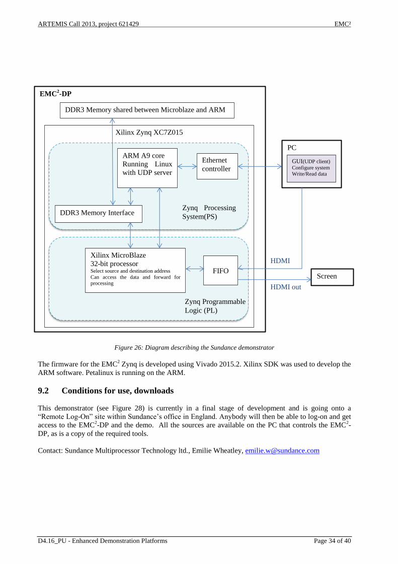
ARTEMIS Call 2013, project 621429 EMC²
D4.16_PU - Enhanced Demonstration Platforms Page 34 of 40
Figure 26: Diagram describing the Sundance demonstrator
The firmware for the EMC2 Zynq is developed using Vivado 2015.2. Xilinx SDK was used to develop the
ARM software. Petalinux is running on the ARM.
9.2 Conditions for use, downloads
This demonstrator (see Figure 28) is currently in a final stage of development and is going onto a
“Remote Log-On” site within Sundance’s office in England. Anybody will then be able to log-on and get
access to the EMC2-DP and the demo. All the sources are available on the PC that controls the EMC
2-
DP, as is a copy of the required tools.
Contact: Sundance Multiprocessor Technology ltd., Emilie Wheatley, [email protected]
EMC2-DP
Xilinx Zynq XC7Z015
Zynq Processing
System(PS)
Zynq Programmable
Logic (PL)
DDR3 Memory Interface
ARM A9 core
Running Linux
with UDP server
Ethernet
controller
Xilinx MicroBlaze
32-bit processor Select source and destination address
Can access the data and forward for processing
DDR3 Memory shared between Microblaze and ARM
FIFO
PC
GUI(UDP client) Configure system
Write/Read data
HDMI
in
HDMI out
Screen

ARTEMIS Call 2013, project 621429 EMC²
D4.16_PU - Enhanced Demonstration Platforms Page 35 of 40
Figure 27: Common WP4 demonstration at the EMC
2 conference Wienna 30.9.2015
Figure 28: Sundance EMC2-DP board with the HDM-IN HDMI-OUT application demo
Figure 27 is presenting results of the WP4 collaboration and development lead by Sundance,
SevenSolution and UTIA at the second EMC2 conference 30.9.2015 in Vienna.
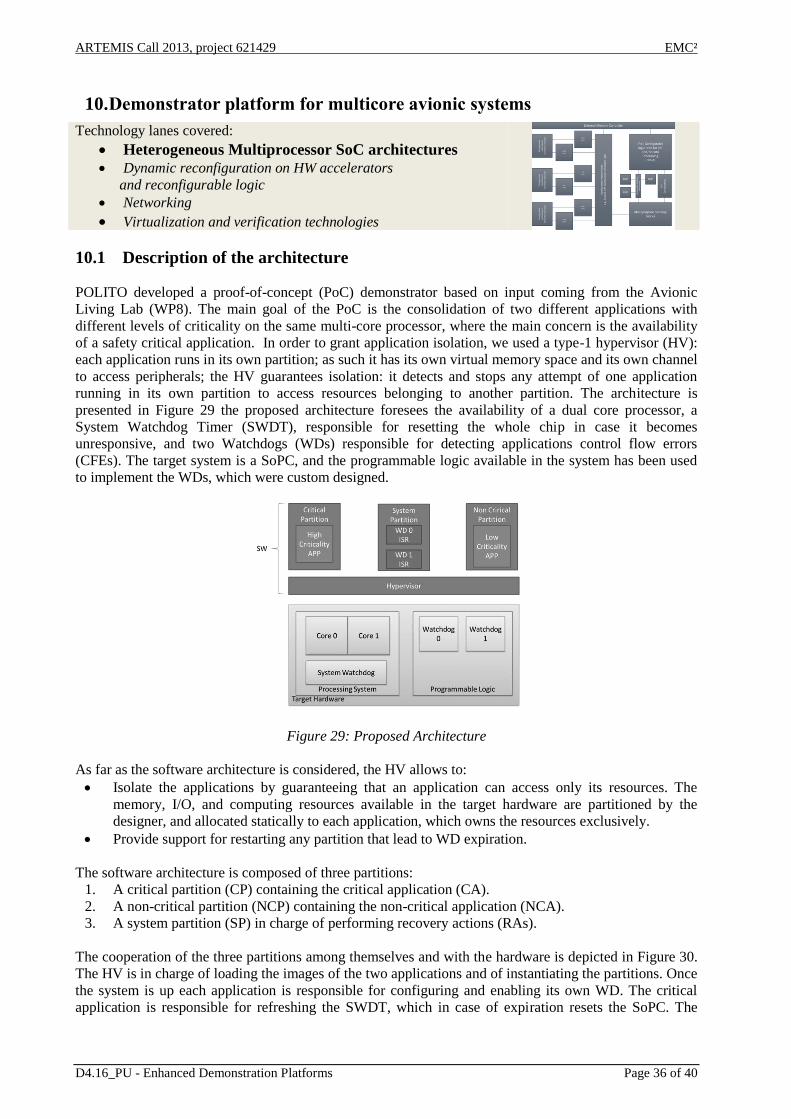
ARTEMIS Call 2013, project 621429 EMC²
D4.16_PU - Enhanced Demonstration Platforms Page 36 of 40
10. Demonstrator platform for multicore avionic systems
Technology lanes covered:
Heterogeneous Multiprocessor SoC architectures
Dynamic reconfiguration on HW accelerators
and reconfigurable logic
Networking
Virtualization and verification technologies
10.1 Description of the architecture
POLITO developed a proof-of-concept (PoC) demonstrator based on input coming from the Avionic
Living Lab (WP8). The main goal of the PoC is the consolidation of two different applications with
different levels of criticality on the same multi-core processor, where the main concern is the availability
of a safety critical application. In order to grant application isolation, we used a type-1 hypervisor (HV):
each application runs in its own partition; as such it has its own virtual memory space and its own channel
to access peripherals; the HV guarantees isolation: it detects and stops any attempt of one application
running in its own partition to access resources belonging to another partition. The architecture is
presented in Figure 29 the proposed architecture foresees the availability of a dual core processor, a
System Watchdog Timer (SWDT), responsible for resetting the whole chip in case it becomes
unresponsive, and two Watchdogs (WDs) responsible for detecting applications control flow errors
(CFEs). The target system is a SoPC, and the programmable logic available in the system has been used
to implement the WDs, which were custom designed.
Figure 29: Proposed Architecture
As far as the software architecture is considered, the HV allows to:
Isolate the applications by guaranteeing that an application can access only its resources. The
memory, I/O, and computing resources available in the target hardware are partitioned by the
designer, and allocated statically to each application, which owns the resources exclusively.
Provide support for restarting any partition that lead to WD expiration.
The software architecture is composed of three partitions:
1. A critical partition (CP) containing the critical application (CA).
2. A non-critical partition (NCP) containing the non-critical application (NCA).
3. A system partition (SP) in charge of performing recovery actions (RAs).
The cooperation of the three partitions among themselves and with the hardware is depicted in Figure 30.
The HV is in charge of loading the images of the two applications and of instantiating the partitions. Once
the system is up each application is responsible for configuring and enabling its own WD. The critical
application is responsible for refreshing the SWDT, which in case of expiration resets the SoPC. The

ARTEMIS Call 2013, project 621429 EMC²
D4.16_PU - Enhanced Demonstration Platforms Page 37 of 40
SWDT is responsible for recovering from faults preventing the execution of recovery actions, e.g. single
event functional interruptions (SEFIs). The non-critical application shall never interfere with the critical
application, therefore only the latter can refresh the SWDT, i.e. the multicore processor is restarted only
when a fault leads to halting the critical application.
WDs are used to detect CFEs; each application partition has a dedicated WD. In our architecture the
application software is partitioned in a number of chunks, each associated with a keyword. The chunks
are executed sequentially and therefore the WD expects to receive the keywords according to a predefined
sequence. The WD stores the keywords the designer defined in its own registers; the number of keywords
in the sequence to be monitored by the WD is also stored in a register. WDs implementation is application
independent: the configuration phase, in which the expected sequence is loaded in each WD, can be
performed either at FPGA configuration time or via software at bootstrap. Moreover, the number of
keywords in the sequence is not bounded to be the same as the WD registers used to store the signatures,
meaning that the number of such registers is merely an upper bound, and one that can be modified by
slightly changing WD’s HDL description. Moreover the time between one signature and the following
one is configurable and is controlled by a timer. The timer is automatically reinitialized with the value
stored in a specific register each time a correct keyword is received. The application is responsible for
sending the keyword of the chunk it is executing to its own WD. Each WD triggers a dedicated interrupt
if:
It has not been enabled and the software sends a keyword;
It has been enabled and the software performs any operation on it except sending a keyword;
It receives a keyword different from the expected one;
Each of the listed conditions corresponds to a control flow error or a data error.
Figure 30: Messages exchanged among architecture components
In general, the architecture implements multiple levels of checks. First, the HV ensures that reserved
resources are not improperly used by the applications running on the computer. This is mainly
implemented through a separation mechanism, which depends on the HV implementation, and through a
time partitioning scheduler. The latter grants that the tasks composing each application are allowed the
proper time to execute, which is determined by the designer through a worst-case execution time analysis.
In case one of these two mechanisms fails, the WDs can detect the problem and allow for a fast recovery
action, which is application dependent. In case WDs are not able to detect or in case the system is in such
a state that a fast recovery action is not possible, the SWDT is able to detect the situation and triggers a
secondary recovery action. Recovery actions are dependent on the application. In avionics applications,
requiring a very high availability, the recovery action is often implemented through the use of an hot-
standby spare computer: when a fault is detected in a computer, its hot-standby spare is activated. The
crew is warned of such event, and the proper maintenance actions are taken in a timely fashion. The
attentive reader may have noticed that the proposed architecture does not allow to avoid the use of spare
computers, however it does allow to reduce the number of computers needed by the avionics, allowing to
implement two applications on a single computer.

ARTEMIS Call 2013, project 621429 EMC²
D4.16_PU - Enhanced Demonstration Platforms Page 38 of 40
10.2 Description of the demonstrator
The proposed architecture has been implemented targeting the Zynq System-on-Programmable Chip
(SoPC), and in particular two versions of the PoC has been developed:
Virtual prototype of the PoC: this version leverages the Mentor Graphics VISTA environment to
build a virtual prototype of the PoC where an instruction-set simulator is used to model the
Cortex A9MP processor embedded in the Zynq device and System C is used to model the
watchdog architecture we developed. Using the VISTA simulator features, a set of fault injection
scripts have been developed.
Physical prototype of the PoC: we modeled the watchdog architecture we devised using the
VHDL language, and we synthesized the proposed architecture on a ZED board. A laptop is
connected to the ZED board via serial cable, as well as via Lauterbach TRACE32 debugger for
I/O and fault injection purposes.
Two versions of the proposed software architecture have been developed based on two different
virtualization platforms: SysGo PikeOS and Mentor Graphics Nucleus secure.
Two applications stemming from the avionic living lab have been integrated on the proposed HW/SW
architecture.

ARTEMIS Call 2013, project 621429 EMC²
D4.16_PU - Enhanced Demonstration Platforms Page 39 of 40
11. Conclusions
Presented enhanced demonstration platforms including basic innovative techniques overview helps to
initiate and implement concrete bottom-up collaborations within WP4 and collaborations with the LL
partners of the EMC2 project.
WP4 team will actively promote this early collection of demonstrators within the EMC2 through the
internal collaborative pages. Several demonstrators have been presented at EMC2 project conference 28-
30.9.2015 in Vienna and discussed at the conference. See Figure 27.

ARTEMIS Call 2013, project 621429 EMC²
D4.16_PU - Enhanced Demonstration Platforms Page 40 of 40
12. References
[1] John McDougall: Simple AMP: Zynq SoC Cortex-A9 Bare-Metal System with MicroBlaze Processor,
XAPP1093 (v1.0.1) January 24, 2014
http://www.xilinx.com/support/documentation/application_notes/xapp1093-amp-bare-metal-microblaze.pdf
[2] Trenz Electronic TE0720-02-2I Series (Z-7020)
http://www.trenz-electronic.de/products/fpga-boards/trenz-electronic/TE0720-02-2I-zynq.html
[3] TE0701 Carrier Board User Manual
https://wiki.trenz-electronic.de/display/4X5B/TE0701+Carrier+Board+User+Manual
[4] Zynq-7000 All Programmable SoC Technical Reference Manual UG585 (v1.8.1)
September 19, 2014
http://www.xilinx.com/support/documentation/user_guides/ug585-Zynq-7000-TRM.pdf
[5] Vivado Web Install Client - 2015.2 Lightweight Installer Download
http://www.xilinx.com/support/download/index.html/content/xilinx/en/downloadNav/vivado-design-
tools/2015-2.html
[6] Software Development Kit Standalone WebInstall Client - 2015.2 Lightweight Installer Download
http://www.xilinx.com/support/download/index.html/content/xilinx/en/downloadNav/embedded-design-
tools/2015-2.html
[7] PicoBlaze 8-bit Embedded Microcontroller User Guide for Extended Spartan 3 and Virtex5 FPGAs;
Introducing PicoBlaze for Spartan-6, Virtex-6, and 7 Series FPGAs.
UG129 June 22, 201.
http://www.xilinx.com/support/documentation/ip_documentation/ug129.pdf
[8] EMC² – ‘Embedded Multi-Core systems for Mixed Criticality applications in dynamic and changeable real-
time environments’ is an ARTEMIS Joint Undertaking project in the Innovation Pilot Programme
‘Computing platforms for embedded systems’ (AIPP5).
http://www.artemis-emc2.eu/
[9] http://www.xilinx.com/support/documentation/application_notes/xapp1093-amp-bare-metal-microblaze.pdf
[10] http://www.xilinx.com/support/index.html/content/xilinx/en/supportNav/boards_and_kits/zynq-
7000_soc_boards_and_kits/zynq-7000_soc_zc702_evaluation_kit.html
[11] “Asymmetric Multiprocessing on ZYNQ with EdkDSP accelerators onXilinx ZC702 board - ISE 14.5”
[12] http://flextiles.eu
[13] http://qt-project.org/wiki/Qt_5.0
[14] AVNET, „HDMI Input/Output FMC Module“ 26 08 2015. [Online]. Available:
http://www.em.avnet.com/en-us/design/drc/Pages/HDMI-Input-Output-FMC-module.aspx
[15] Sundance, „EMC2-DP – PC/104 ONEBANK CARRIER FOR SOC MODULES,“ 26 08 2015. [Online].
Available: http://www.sundance.technology/som-cariers/pc104-boards/emc2-dp/
[16] AVNET, „ON Semiconductor Image Sensor with HDMI Input/Output FMC Bundle,“ 26 08 2015. [Online].
Available: http://www.em.avnet.com/en-us/design/drc/Pages/OnSemi-Image-Sensor-with-HDMI-Input-
Output-FMC-bundle.aspx.
[17] Trenz, „Trenz WiKi - Lattice CPLD Programming,“ 25 08 2015. [Online]. Available: https://wiki.trenz-
electronic.de/display/4X5B/TE0701+JTAG+Programming+Guide#TE0701JTAGProgrammingGuide-
LatticeCPLDProgrammingLatticeCPLD
[18] El Salloum, C., Elshuber, M., Höftberger, O., Isakovic, H., & Wasicek, A. (2013). The ACROSS MPSoC -
A new generation of multi-core processors designed for safety-critical embedded systems. Microprocess.
Microsyst., 37(0141-9331), 0141-9331.
[19] VMware Workstation 12 Player for Windows 64-bit. https://www.vmware.com/products/player/playerpro-
evaluation
[20] SDSoC - 2015.2 Full Product Installation - 2015.2 Full Product Installation
http://www.xilinx.com/support/download/index.html/content/xilinx/en/downloadNav/sdx-development-
environments/sdsoc/2015-2.html
[21] Vivado Lab Edition - 2015.2 Full Product Installation
http://www.xilinx.com/support/download/index.html/content/xilinx/en/downloadNav/vivado-design-
tools/2015-2.html