current mirror. a mos transistor biased by a resistive divider sensitivity to vdd, resistor...
TRANSCRIPT

Current Mirror
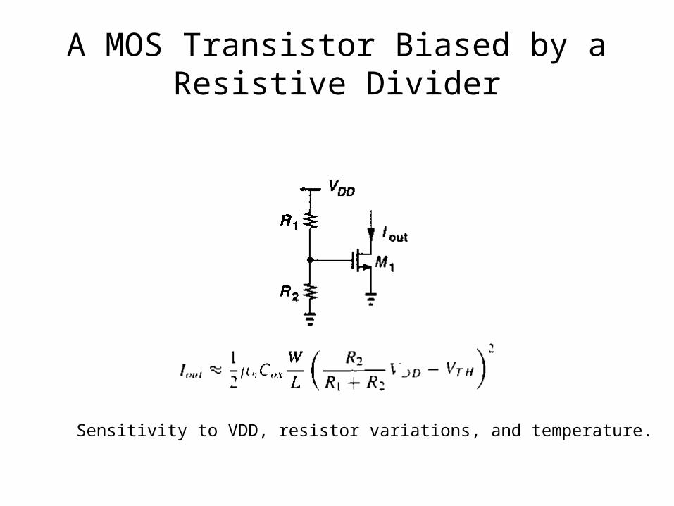
A MOS Transistor Biased by a Resistive Divider
Sensitivity to VDD, resistor variations, and temperature.
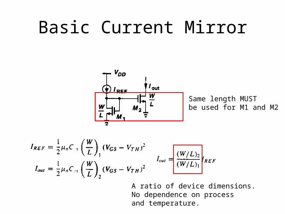
Basic Current Mirror
A ratio of device dimensions.No dependence on processand temperature.
Same length MUSTbe used for M1 and M2

Current Mirror Used to Bias a Differential Amplifier
Reduce gm by reducing current rather than the aspect ratio.Reduce I(M3) and I(M4).
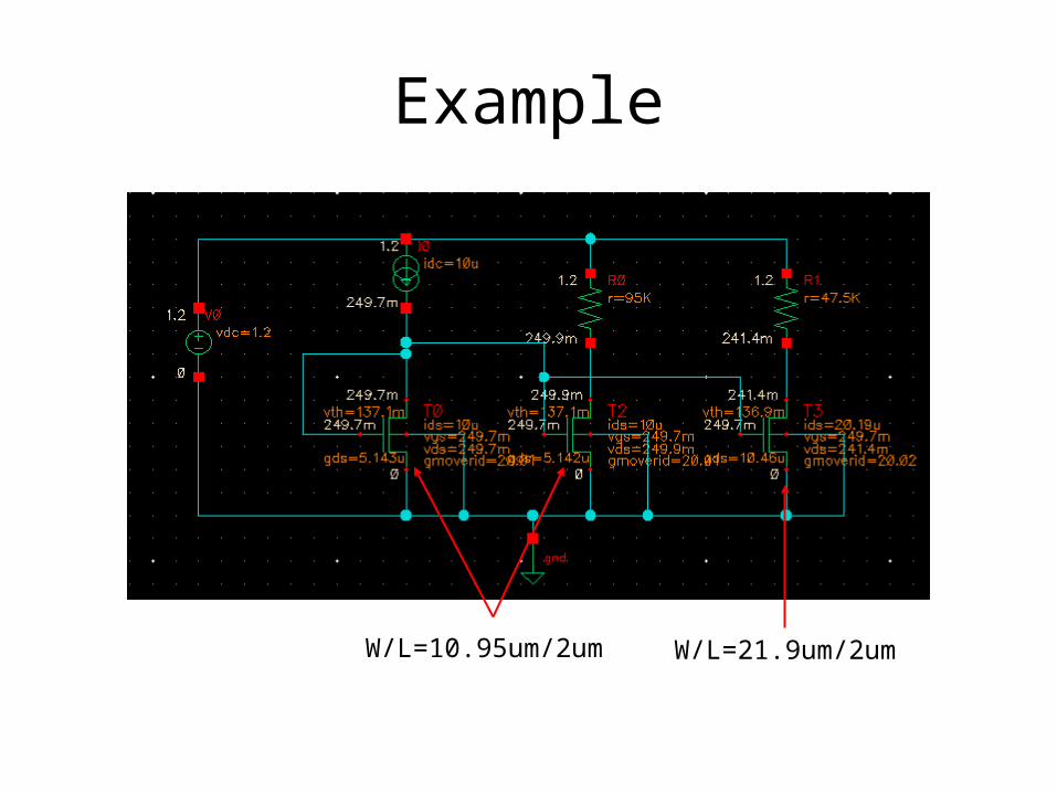
Example
W/L=10.95um/2um W/L=21.9um/2um

Trade-Offs
• Output resistance (1/gds)• CDS• W/L• Current

IOUT=100 uA
L(um) W(um) GDS (uS) CDS (fF)
2 109.63 51.82 100.39
800n 47.4 56.5 17.13
180n 17.02 92.9 1.079
120n 13.33 147 0.411
For Same IOUT, L↓→W↓→GDS↑(Ro↓) →CDS ↓
Drop in Ro is not desired.

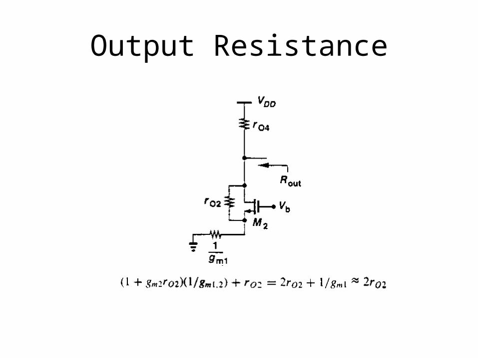
Use Cascode to Increase output Resistance
Rout is approximately gm3ro3ro2
L1=L2, but L3 need not equal to L2.
Design Criteria: Choose Vb so that VY and VX.

Cascode Current Source
Requirement: Choose Vb so that VX=VY
VN=VGS0+VX=VGS3+VY
Therefore, VGS3=VGS0
Since ID1=ID2, (W/L)3=(W/L)0
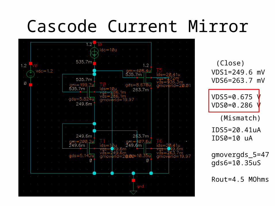
Cascode Current Mirror
VDS1=249.6 mVVDS6=263.7 mV
VDS5=0.675 VVDS0=0.286 V
IDS5=20.41uAIDS0=10 uA
gmovergds_5=47gds6=10.35uS
Rout=4.5 MOhms
(Mismatch)
(Close)

Sensitivity of IOUT due to VOUT
As VX decreases from VDD,M3 enters the triode region first.
M2 enters the triode region

Sweep Output Voltage
VTH5=177.6 mVVG5=535.7 mVVG6=249.6 mVVTH6=136.9 mV
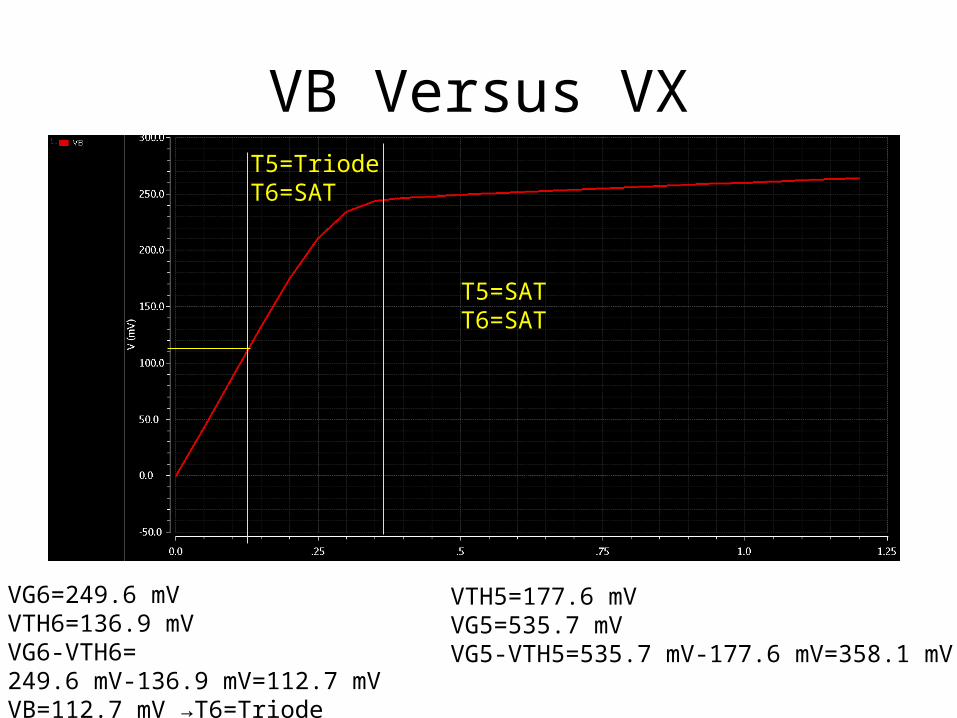
VB Versus VX
VTH5=177.6 mVVG5=535.7 mVVG5-VTH5=535.7 mV-177.6 mV=358.1 mV
T5=SATT6=SAT
T5=TriodeT6=SAT
VG6=249.6 mVVTH6=136.9 mVVG6-VTH6=249.6 mV-136.9 mV=112.7 mV VB=112.7 mV →T6=Triode
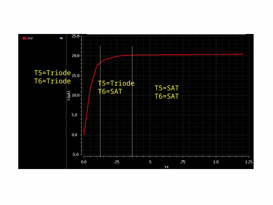
T5=SATT6=SAT
T5=TriodeT6=SAT
T5=TriodeT6=Triode
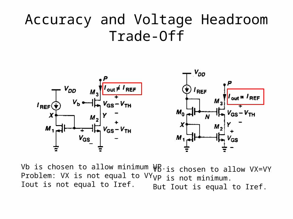
Accuracy and Voltage Headroom Trade-Off
Vb is chosen to allow minimum VP.Problem: VX is not equal to VYIout is not equal to Iref.
Vb is chosen to allow VX=VYVP is not minimum.But Iout is equal to Iref.

Design Criteria• Desirables:– IOUT should be IREF. (i.e. VX=VY)
– Vout should be minimized. (i.e. VOD2+VOD3)
VOUT=VOD3+VOD4
VA=VB→IOUT=mIREF
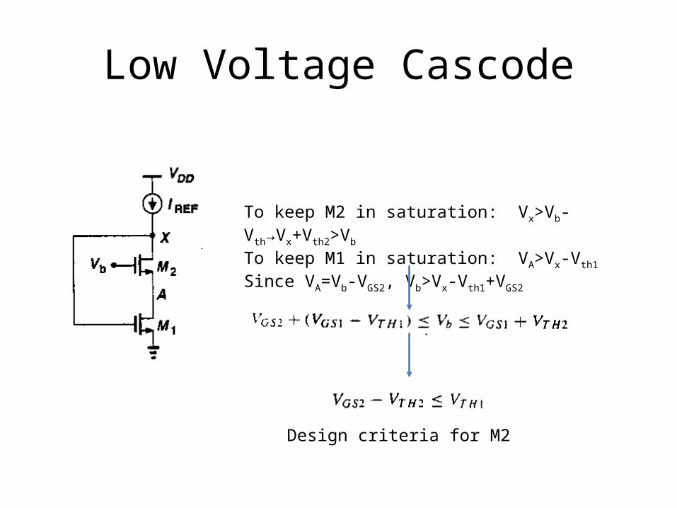
Low Voltage Cascode
To keep M2 in saturation: Vx>Vb-Vth→Vx+Vth2>Vb
To keep M1 in saturation: VA>Vx-Vth1
Since VA=Vb-VGS2, Vb>Vx-Vth1+VGS2
Design criteria for M2
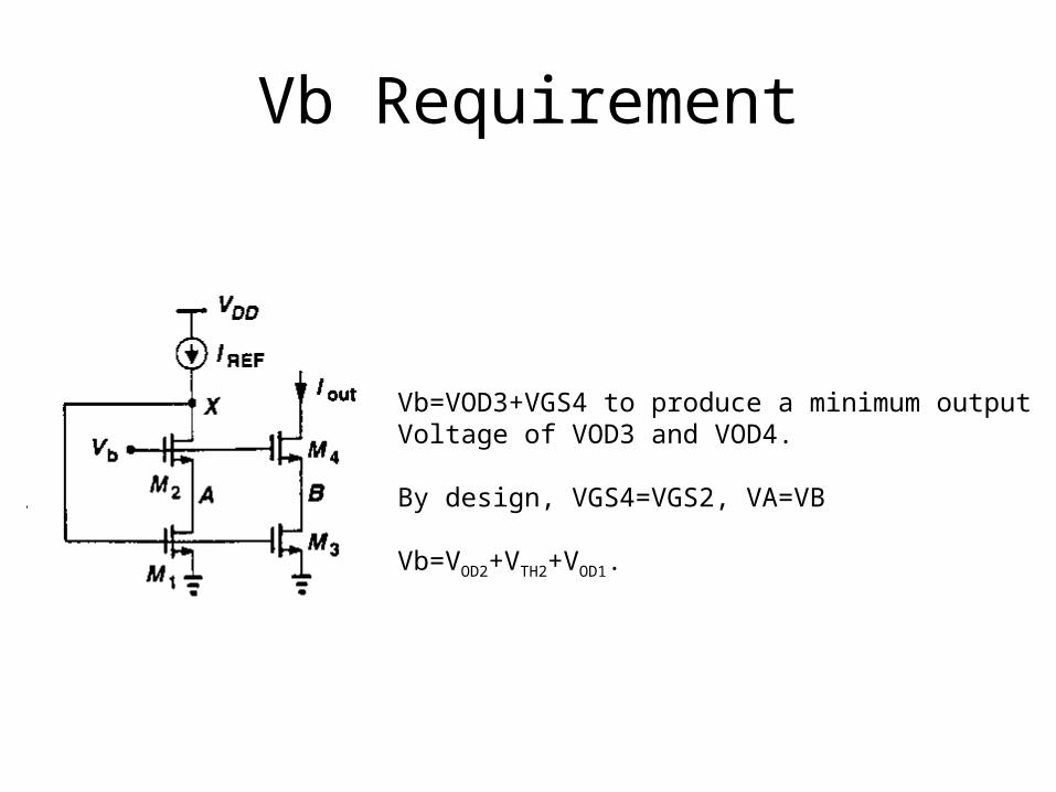
Vb Requirement
Vb=VOD3+VGS4 to produce a minimum outputVoltage of VOD3 and VOD4.
By design, VGS4=VGS2, VA=VB
Vb=VOD2+VTH2+VOD1.

Minimum Vout
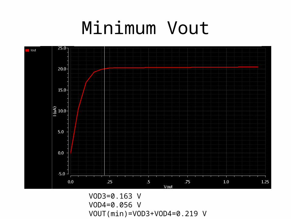
Minimum Vout
VOD3=0.163 VVOD4=0.056 VVOUT(min)=VOD3+VOD4=0.219 V
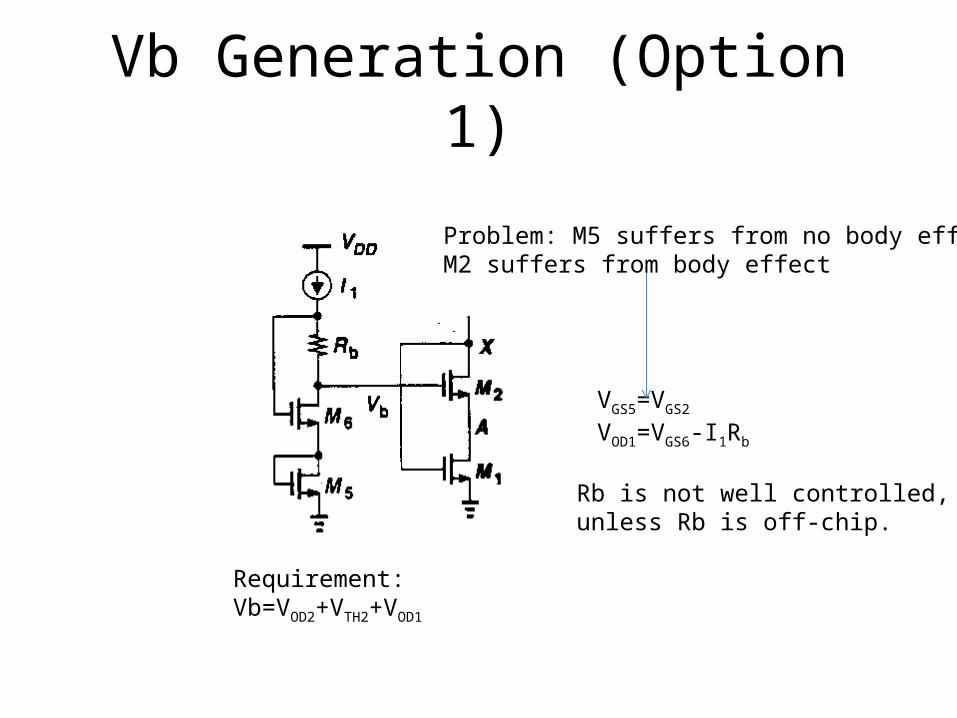
Vb Generation (Option 1)
Requirement:Vb=VOD2+VTH2+VOD1
VGS5=VGS2
VOD1=VGS6-I1Rb
Problem: M5 suffers from no body effectM2 suffers from body effect
Rb is not well controlled,unless Rb is off-chip.

Vb Generation (Option 2)
Requirement:Vb=VOD2+VTH2+VOD1
VGS5=VGS2
VOD1=VGS6-VTH7
Problem: M5 suffers from no body effectM2 suffers from body effect
Design M7 (Large W7/L7) so that VGS7 is approx. VTH7
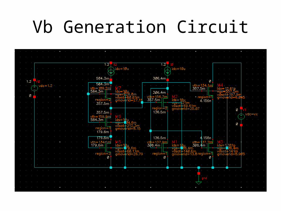
Vb Generation Circuit
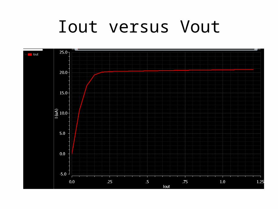
Iout versus Vout

Active Current Mirror

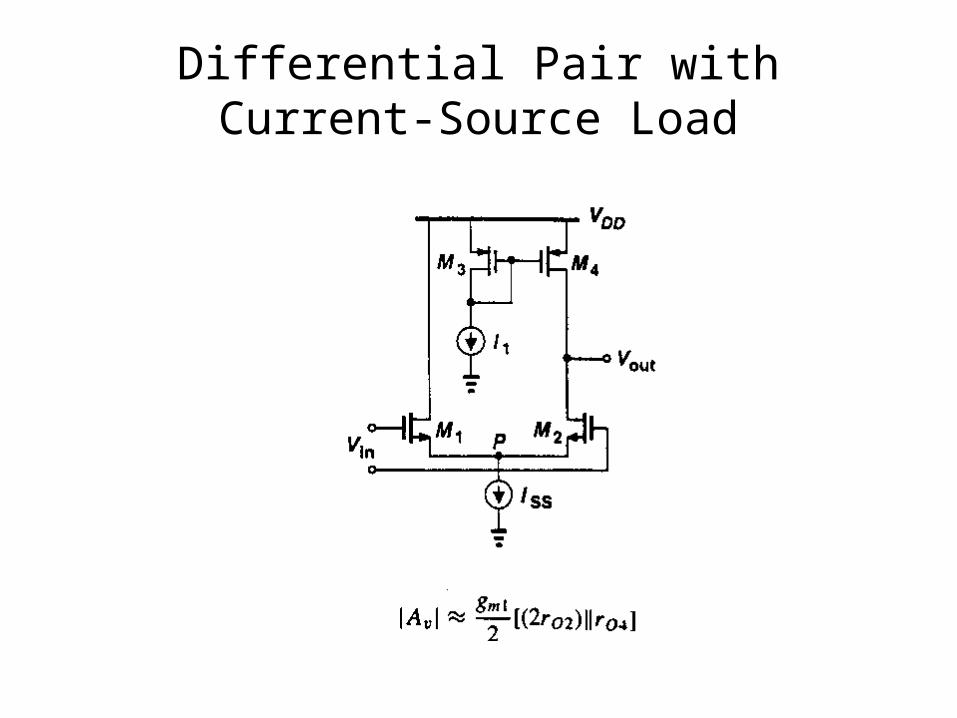
Differential Pair with Current-Source Load
Calculate the Av via Norten Equivalent Circuit
(The half-circuit concept is not applicable due to lack of symmetry)

Transconductance
Gm=gm1/2
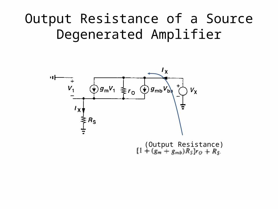
Output Resistance of a Source Degenerated Amplifier
(Output Resistance)
Output Resistance
Differential Pair with Current-Source Load
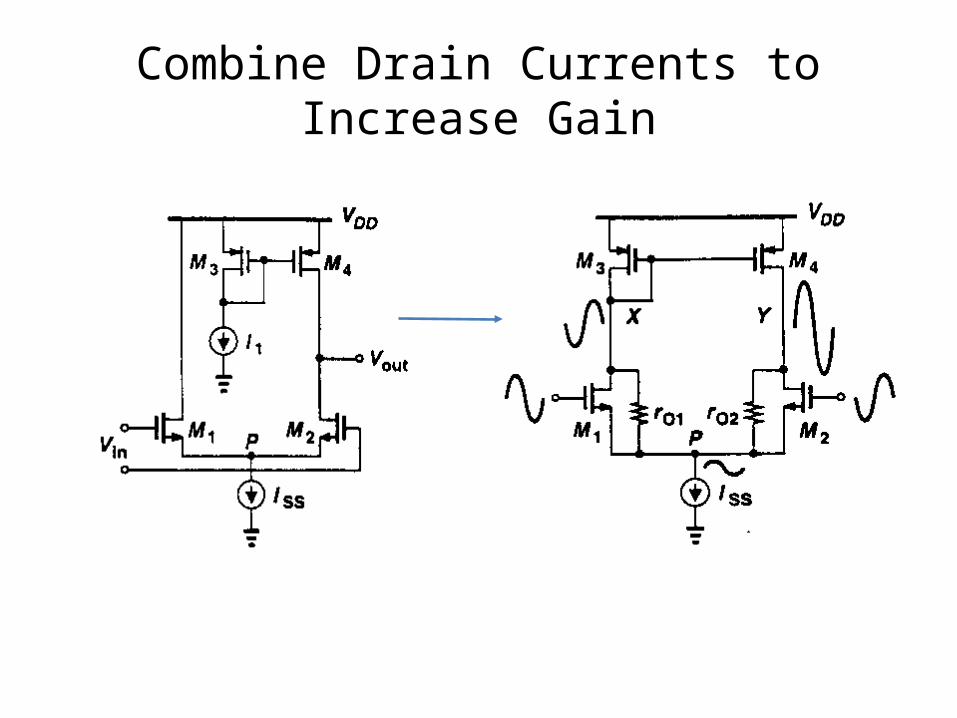
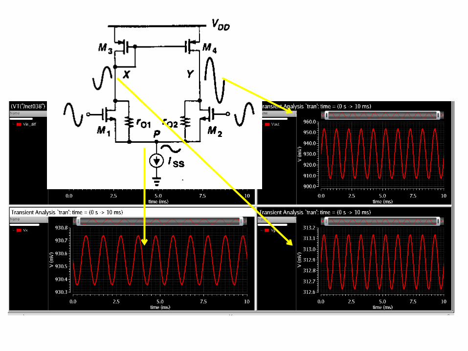
Combine Drain Currents to Increase Gain

Output DC Voltage
With perfect symmetry VX,DC=VY,DC.
VX=VDD-|VGS3|If VY < VX, then IM2<IM1.Since IM3=IM1 and IM4=IM2, IM3>IM4. This is not possible because VSD4>VSD3, so IM4> IM3.

Small Signal Gain
The swing at X is low since the impedance at X is 1/gm3.So the X can be approximated as an AC ground for the purpose calculating Gm.
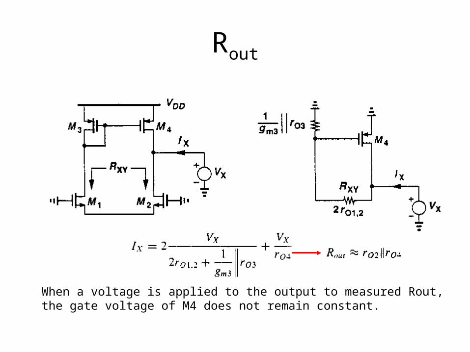
Rout
When a voltage is applied to the output to measured Rout,the gate voltage of M4 does not remain constant.
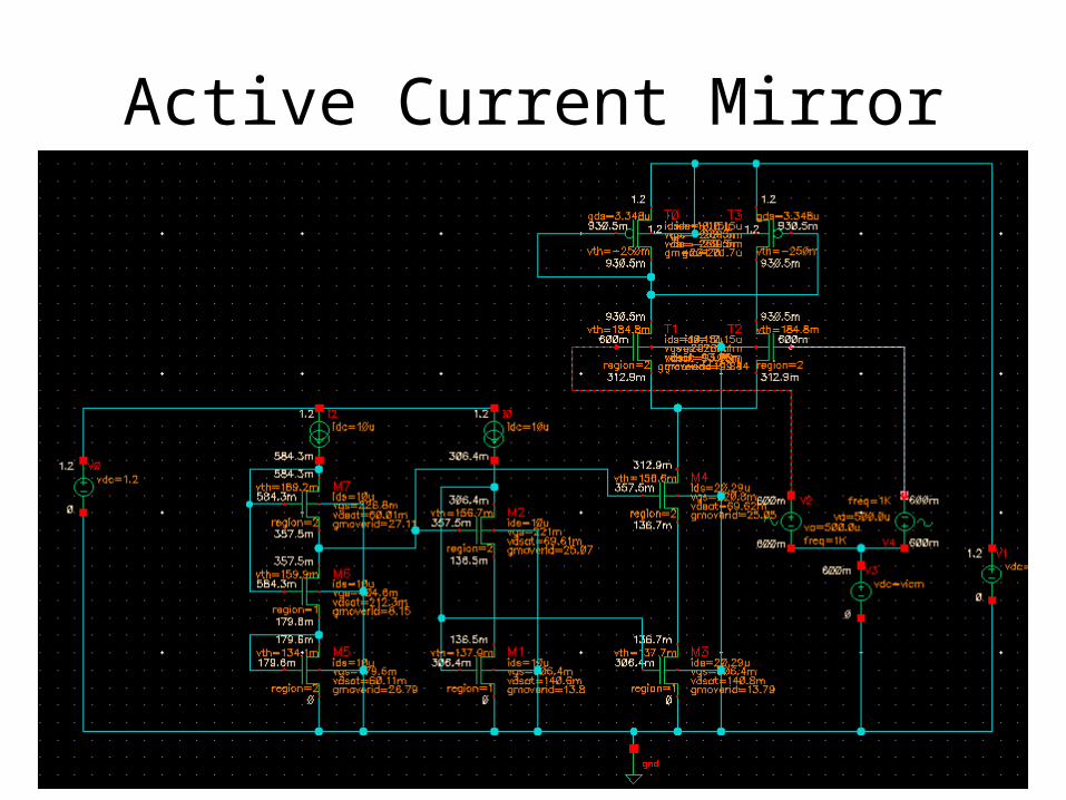
Active Current Mirror

Voltage Gain of Active Current Mirror
Vin,pp=2 mVVout,pp=46.69 (Simulation)Vout,pp=47.21 mV (Analytical calculation)

Common Mode Operation
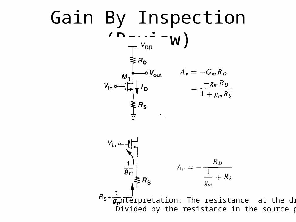
Gain By Inspection (Review)
Interpretation: The resistance at the drainDivided by the resistance in the source path
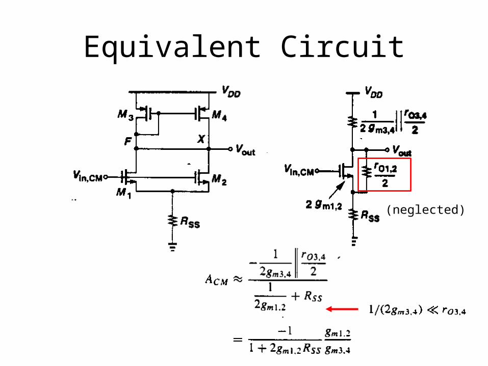
Equivalent Circuit
(neglected)

Vout,pp=0.003414m V
Vin,pp=2 mV Av=0.001707
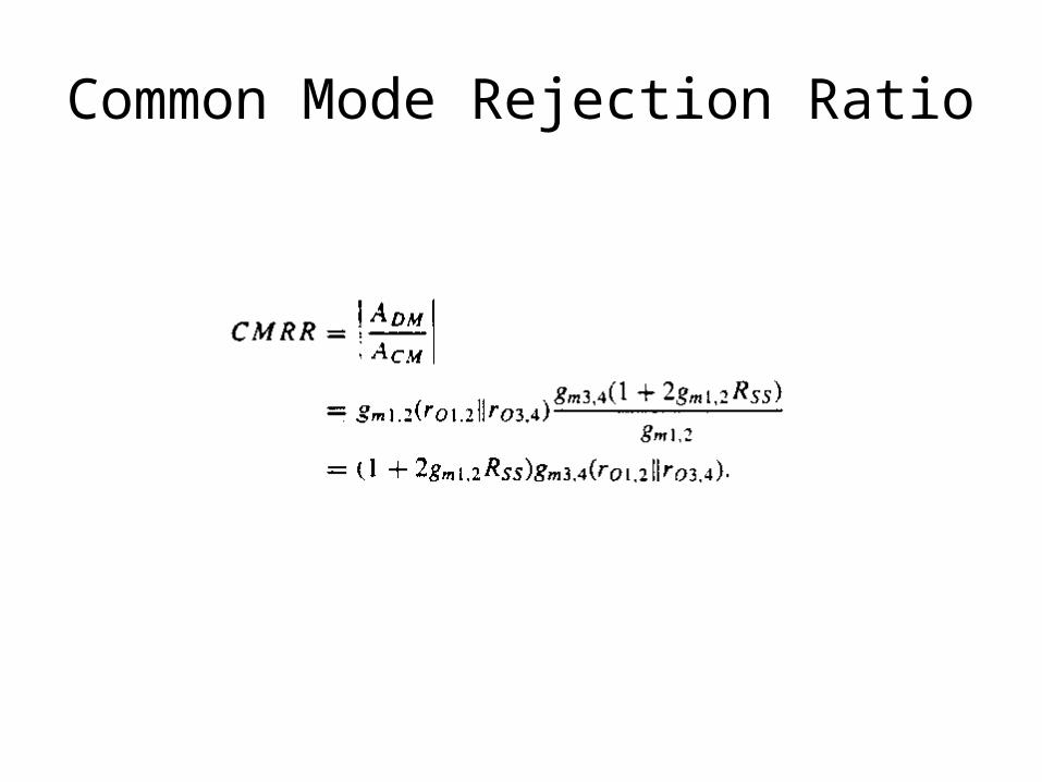
Common Mode Rejection Ratio
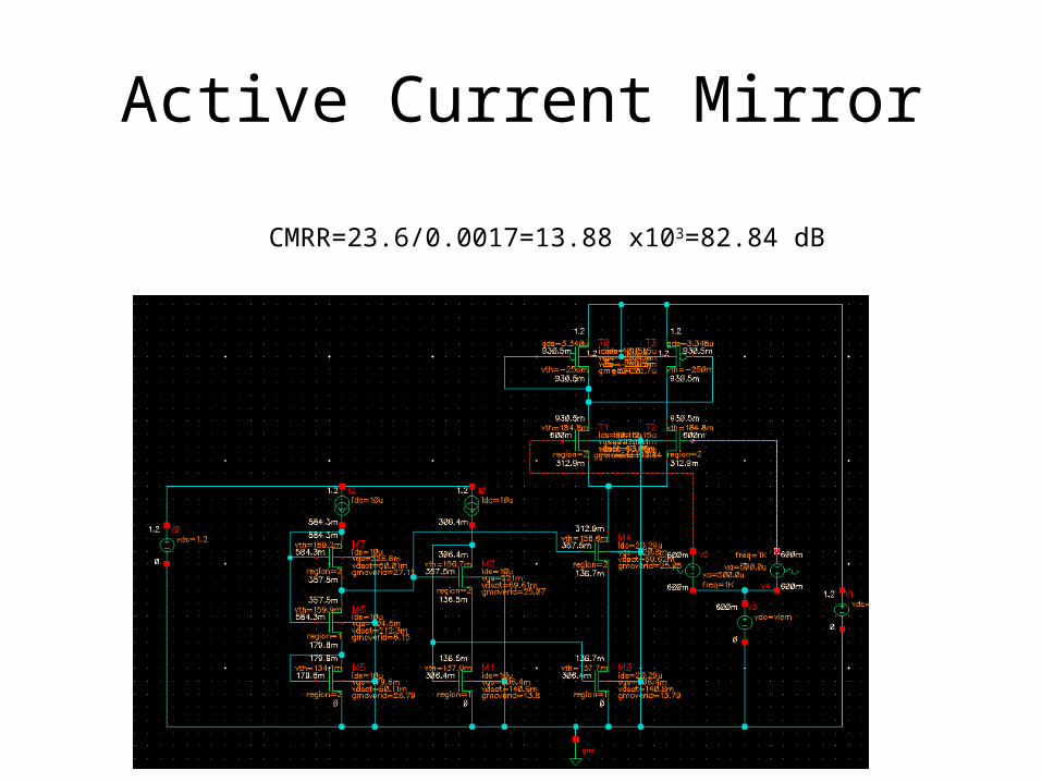
Active Current Mirror
CMRR=23.6/0.0017=13.88 x103=82.84 dB