csus college of engineering and computer...
TRANSCRIPT
CSUS COLLEGE OF ENGINEERING ANDCOMPUTER SCIENCE
DEPARTMENT OF ELECTRICAL AND ELECTRONICENGINEERING
EEE 102L – Analog/Digital ElectronicsLaboratory
Laboratory Manual
Spring 2007

2
Table of ContentsEEE 102L Analog/Digital Electronics Laboratory – Course Outline 3EEE 102L Parts Kit – Fall 2004 5Objectives and Goals of the Laboratory 6Laboratory 1 – Introductory PSpice Programming Assignment 9Laboratory 2 – Introduction to LabVIEW 10Notes Concerning the Operation of the HP Signal Generators 19Laboratory 3 – Exploration of Diode Characteristics 20Laboratory 4 – Diode Circuits 24Laboratory 5 – MOSFET Transistor Characteristics 27Laboratory 6 – BJT Transistor Characteristics 31Laboratory 7 – Common-Emitter Amplifier Design 35Laboratory 8 – OP Amp Instrumentation Amplifiers and First Order Filters 37Appendix 41

3
EEE 102L Analog/Digital Electronics Laboratory
Service Course
2006 – 2008 Catalog Data: EEE 102L. Analog/Digital Electronics Laboratory. Introduction to analog/digitalelectronics, diodes, FET's, BJT's, DC biasing, VI characteristics, single stage amplifiers, power supplies and voltageregulators, power electronic devices, OP-amps, active filters, A/D and D/A converters. PSPICE used extensively.Note: Cannot be taken for credit by E&EE Majors. Prerequisite: ENGR 017. Corequisite: EEE 102. 1 unit.
Text: Jaeger, R.C., Microelectronic Circuit Design, 2nd Edition, McGraw-Hill, 2004, ISBN 0-07-232099-0
Support Software: Herniter, M.E., Schematic Capture with Cadence PSpice, Prentice-Hall, 2nd Edition, 2003,ISBN 0-13-048400-8.
Course Goals:
1. To reinforce learning in the accompanying EEE 102 course through hands-on experience with electroniccircuit analysis, design, construction, and testing.
2. To provide the student with the capability to use LabVIEW and PSpice software as tools in electroniccircuit analysis and design, and in future courses, design projects, and professional work assignments.
Prerequisites by Topic:
1. General knowledge of a structured programming language (i.e. C++).2. Basic physical concepts of electricity and magnetism.3. Basic circuit analysis concepts and procedures.
Topics Covered/Class Schedule/Evaluation:
Topics
1. Introduction to Software Tools and Workstation Equipment: Introduction to PSpice Schematic CircuitConstruction and Analysis; Introduction to LabVIEW Virtual Instrument Workstation Operation and A/DConversion
2. Solid State Diodes and Diode Circuits: Diode Characteristics in Forward and Reverse Bias Conditions;Power Supplies and Wave Shaping Circuits
3. Field Effect Transistors: FET Characteristics; Operating Regions and Characteristics of NMOS Devices;MOSFET Biasing Circuits, Analysis, Design, Construction, Testing, and Simulation
4. Bipolar Junction Transistors: Operating Regions and Characteristics of the BJT; Forward-Active RegionAnalysis and Design; BJT Biasing Circuits, Analysis, Design, Construction, Testing, and Simulation
5. Small-Signal Modeling and Linear Amplification: The BJT Common-Emitter Amplifier Analysis, Design,Construction, Testing and Simulation
6. Operational Amplifiers: The Differential Amplifier; Frequency Response; Input/Output Impedance;Instrumentation Amplifiers; Common Mode Signal Analysis; Active Filters
Course Outline
Week Topic Lab # Report Due
1 Introduction to the Lab none2 Introduction to PSpice 1
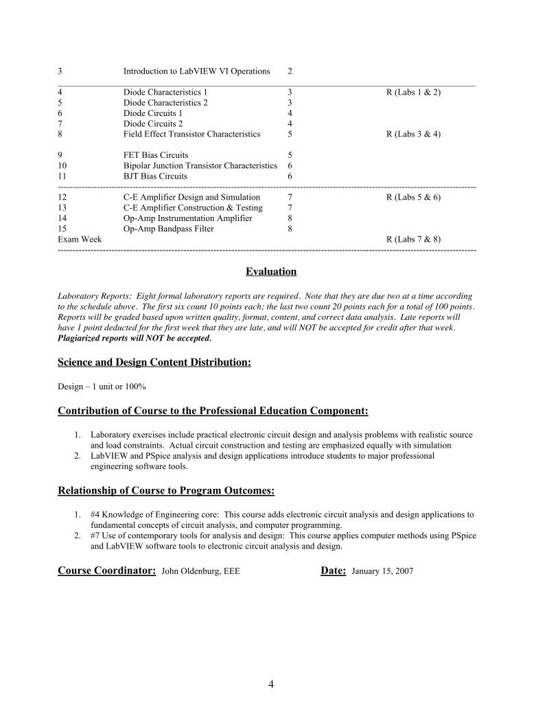
4
3 Introduction to LabVIEW VI Operations 2_____________________________________________________________________________________________4 Diode Characteristics 1 3 R (Labs 1 & 2)5 Diode Characteristics 2 36 Diode Circuits 1 47 Diode Circuits 2 48 Field Effect Transistor Characteristics 5 R (Labs 3 & 4)
9 FET Bias Circuits 510 Bipolar Junction Transistor Characteristics 611 BJT Bias Circuits 6--------------------------------------------------------------------------------------------------------------------------------------------12 C-E Amplifier Design and Simulation 7 R (Labs 5 & 6)13 C-E Amplifier Construction & Testing 714 Op-Amp Instrumentation Amplifier 815 Op-Amp Bandpass Filter 8Exam Week R (Labs 7 & 8)--------------------------------------------------------------------------------------------------------------------------------------------
Evaluation
Laboratory Reports: Eight formal laboratory reports are required. Note that they are due two at a time accordingto the schedule above. The first six count 10 points each; the last two count 20 points each for a total of 100 points.Reports will be graded based upon written quality, format, content, and correct data analysis. Late reports willhave 1 point deducted for the first week that they are late, and will NOT be accepted for credit after that week.Plagiarized reports will NOT be accepted.
Science and Design Content Distribution:
Design – 1 unit or 100%
Contribution of Course to the Professional Education Component:
1. Laboratory exercises include practical electronic circuit design and analysis problems with realistic sourceand load constraints. Actual circuit construction and testing are emphasized equally with simulation
2. LabVIEW and PSpice analysis and design applications introduce students to major professionalengineering software tools.
Relationship of Course to Program Outcomes:
1. #4 Knowledge of Engineering core: This course adds electronic circuit analysis and design applications tofundamental concepts of circuit analysis, and computer programming.
2. #7 Use of contemporary tools for analysis and design: This course applies computer methods using PSpiceand LabVIEW software tools to electronic circuit analysis and design.
Course Coordinator: John Oldenburg, EEE Date: January 15, 2007

5
EEE 102L Parts Kit – Spring 2005
Resistors 1/4 W, Carbon Film, 5%
Qty. Value3. 10 Ω2 15 Ω1 22 Ω1 33 Ω2 51 Ω2 100 Ω1 150 Ω1 220 Ω1 330 Ω2 510 Ω1 680 Ω1 820 Ω2 1K Ω1 1.2Κ Ω4 1.5Κ Ω1 2.2Κ Ω1 3.3Κ Ω2 5.1Κ Ω1 6.8Κ Ω1 8.2Κ Ω6 10Κ Ω1 12Κ Ω6 15Κ Ω2 20Κ Ω2 30Κ Ω2 51Κ Ω1 68Κ Ω1 82Κ Ω4 100Κ Ω1 120Κ Ω4 150Κ Ω2 200Κ Ω2 300Κ Ω2 510Κ Ω1 680Κ Ω1 820Κ Ω2 1.0Μ Ω2 5.1Μ Ω2 10Μ Ω
Capacitors
Qty. Value Description1 22 pF Ceramic Disc, 500 V1 220 pF Ceramic Disc, 500 V1. 2200 pF Ceramic Disc, 500 V2. 0.01 µF Ceramic Disc, 1002 0.1 µF Ceramic Disc, 50 V2 1 µF Metallized Poly Film, 250 V
(Digikey P10979-ND)2 10 µF Metallized Poly Film, 100 V
(Digikey EF1106-ND)1 47 µF Radial Electrolytic, 25 V1 100 µF Radial Electrolytic, 25 V1 220 µF Radial Electrolytic, 25 V1 1000 µF Radial Electrolytic, 16 V
Diodes/Rectifiers
Qty. Description1 1N4001 Si Rectifier1 W005G Bridge Rectifier3 1N914 Si Switching Diode1 1N4734A 5.6V, 1W Zener Diode
Transistors
Qty. Description1 2N2222A NPN Transistor (TO-9)1 IRF630A NMOS FET Power Transistor
Integrated Circuits
Qty. Description1 Burr-Brown INA118P Instrumentation
Amplifier2 LM741N Operational Amplifier1 CD4007 CMOS Dual Complementary
Pair/Inverter
Miscellaneous
Qty. Description5' 22AWG Hook-up Wire, Blue5' 22AWG Hook-up Wire, Yellow2 9V Battery Clip
Note: A Standard pin-socket protoboard is required, but not included in the kit. A smallone costing $5-$7 is sufficient and available at Radio Shack, Newark or Fry’s Electronics
6
CSUS College of Engineering and Computer ScienceDepartment of Electrical & Electronic EngineeringEEE 102L Analog/Digital Electronics Laboratory
OBJECTIVES AND GOALS OF THE LABORATORY
The laboratory for this course has two major objectives: 1) To acquaint you with virtualinstrument technology for electronic circuit design and testing, and 2) to introduce you to thesimulation and physical circuit behavior of basic electronic devices and circuits. At the end ofthe course, you should have acquired knowledge of the fundamental principles of electroniccircuits and gained considerable facility in making time and frequency domain measurementsusing modern electronic instrumentation.
GENERAL LABORATORY POLICIES
1. All laboratory work will be done in student pairs or a group of three. Each student will berequired to submit an individual laboratory report.
2. You are strongly urged to read the reference material and perform any pre-lab workspecified in the laboratory handout before you come to the lab. In many cases, you will need thisknowledge in order to efficiently plan your methods of investigation and finish the lab in thetime allotted.
3. The laboratory instructions will specify the information required in the laboratory report;however, you are not restricted to providing only this information and the inclusion of commentsabout the validity of the data and an appendix of relevant analytical work is strongly encouraged.
Laboratory Report Format
a. Introduction -- give a one - two paragraph overview, in your own words, whichdescribes the topic covered in the laboratory. This should be complete and concise.
b. Procedure Notes -- note any changes (voluntary or required by circumstance) from theprocedure in the handout, which you feel may have had a significant bearing on theresults. You don't need to repeat procedures described in the laboratory instructions.
c. Data and Results -- include all data specified in the handout. Use tables and graphswhere appropriate. Figures (pictures, tables, graphs, etc.) should each have a completefigure "legend" which briefly describes the relevant information in the figure. Stateresults CLEARLY. Describe your results and answer any specific questions asked in thehandout in this section. You may choose to include analytical work in an appendix tosupport your results. In cases where “pictures” of VI front panels have been taken todocument results, you may insert them directly as figures in a Microsoft Word laboratoryreport document.

7
d. Conclusions -- did your results agree with or differ from what you might haveexpected from lecture and/or your readings? Comment, as part of your conclusions,about the value of the laboratory exercise with respect to its improvement of yourunderstanding of the subject material.
e. Appendix -- include relevant analytical calculations and any miscellaneous additions.
4. Laboratory reports must be “hard copy” format and will be due one week following the end ofthe scheduled laboratory exercise (see the schedule of laboratories in the EEE 102L CourseOutline), or as determined by your instructor. They will be graded based upon completeness andthe quality of both the analysis and documentation. Reports will have one point deducted forthe first week that they are late. Reports more than one week late will NOT be accepted.Plagiarized reports will NOT be accepted.
5. Almost all necessary equipment will be found at the computer workstations in the laboratory.Any other equipment of a general nature that you may desire (DVMs, Capacitance Checkers,Transformers, etc.), if not provided already at the lab station, may be requested from theinstructor (only during scheduled laboratory periods). A selection of electronic parts that youwill need is available as an EEE 102L Parts Kit, and may be obtained from your LaboratoryInstructor. Obtain a Parts Kit Purchase Form from the EEE 102L Web page. You must pay forthe parts kit and get a receipt at the Cashier’s Window in Lassen Hall. Give your receipt to thelab instructor in exchange for a parts kit. Resistors, potentiometers, capacitors, diodes,transistors, op-amps, ICs, hook-up wire, and 9V battery clips are included. You are also free topurchase what you need from suppliers such as Radio Shack, Fry or Newark Electronics in town,or to use any applicable electronics parts that you may already own.
6. Starting in week 3, you will be required to have the Parts Kit for circuit construction.You may share the cost of one kit with your lab partner(s). You and your lab partner(s) shouldalso purchase a suitable (two strips of terminals are sufficient) protoboard if you don't alreadyown one (estimated cost is $5 - $7 at the electronics suppliers mentioned above), and two 9Valkaline batteries to use as a power supply in the last lab exercise. You will find that having yourown protoboard will be helpful in many other laboratories in the CpE program, and will be wellworth the expense.
7. As a registered EEE 102L student, you will be issued the undergraduate student lock code toRVR-5017. You have the responsibility to keep that code to yourself and to use the laboratoryonly for the purposes of the course. You have priority use of workstations in the VI Laboratoryduring the scheduled hours for the laboratory portion of the course. In general however, the labis not crowded and you should have good access to the equipment at other times.
Open Laboratory Rules for RVR-5017
1. Your open access to this laboratory is being granted under the assumption that you willconduct your activities there as a professional engineer and according to the following rules.

8
2. You should not admit anyone except yourself to the laboratory. It is for your use for thepurposes of the course you are taking and for no other purpose.
3. No eating or drinking in RVR-5017. Computers are very sensitive to spills!
4. The Macintosh workstations are primarily for support of LabVIEW and PSpiceprogramming/applications. They also have Microsoft Office available for laboratory documentpreparation. Surfing the Net, E-mail and Instant Messaging, and other workstation needs shouldbe met using your own personal computer or those in “open” laboratories on the campus. To becourteous to other students who will follow you, please leave the desktop of the workstation withall icons in the default condition when you are finished with your work. Please empty yourtrash!
5. Report any equipment malfunctions to your instructor as soon as it is practical to do so.
6. No equipment, manuals, etc. may be removed from the laboratory without approval of theinstructor. Peripheral equipment (PARTICULARLY TEST CABLES AND CONNECTORS)associated with each workstation MUST remain with that station.
7. Times for use of RVR-5017 are posted on the door of the laboratory. Instructor help will beavailable in the lab only during scheduled hours for the course.
8. Violation of the lab rules may result in our having to close the laboratory and restrict your useof it only to scheduled laboratory hours. Please act professionally and responsibly!
9
Laboratory 1 – Introductory PSpice Programming Assignment
Your goal is to complete a brief, self-instructional introduction to PSpice programming duringthis laboratory, and to become familiar with the Macintosh workstations and the operation of thesoftware under VirtualPC. You will use chapters 1 and 3 of Herniter, M.E., Schematic Capturewith Cadence PSpice, 2nd Edition, Prentice Hall, 2003 as your guide. Please read this materialcarefully before the lab period so that you can minimize the time required to complete the work.
1. Check to see that your workstation monitor is on standby (yellow light on). If the monitor isoff, turn it on before you boot up the workstation. Start up your Macintosh workstation bypressing the gray power button on the front of the chassis. Cadence PSpice software is installedon the Virtual PC partition on the Macintosh workstations. Find Virtual PC under the AppleMenu (). Open Virtual PC by double clicking on its icon. When Virtual PC is fully loadedyou will see a window on the Macintosh desktop that looks like a familiar Windows 2000Professional desktop. Under Start/Programs/, you will find the Cadence PSpice Softwareorganized as described in Chapter 1 of the Herniter text. There is a shortcut icon on the desktopthat will get you to the software very quickly. Alternately, (and highly preferred) you mayinstall the Cadence Pspice, which accompanies the Herniter text, on your home workstation andcomplete this introduction as described. However, do not neglect to use the lab period to becomefamiliar with the Macintosh workstations, since you will be using them in subsequent laboratorysessions. Follow the circuit schematic creation and dc nodal analysis instructions provided inchapters 1 and 3 (up to but not including Exercise 3-1). You may skip the section J onformatting the title block, and section M on creating hierarchical designs in chapter 1. When youare finished, select Save All and Quit from the Macintosh File menu. This will save the currentstate of the VirtualPC and allow it to be quickly started again.
2. Files can be moved to different workstations in the laboratory by placing them in the VoyagerTemporary server partition. That partition is accessible from virtually any computer connectedto the ECS network. When your project is complete, save it (the entire project partition with allsupporting files) as an appropriately named file on your personal USB Flash Drive (highlyrecommended). You may FTP your file to a secure personal account using the FETCH utilityunder the Apple menu or transfer it to the Voyager Temporary partition and access it from anynetworked workstation. Only a hard copy picture of your final circuit schematic, as it stands atthe end of the chapter 3 section of the Herniter text, is required as a “report” for this firstlaboratory exercise. (See “Procedure for Taking Pictures of the Active Window on MacintoshWorkstations in the appendix of this lab manual.)
3. Your file should be submitted to your instructor, on or before the due date for the first report(R) on the schedule.
4. You will score 10 points for successful completion of the PSpice assignment. One point willbe deducted during the first week after the date due for late submissions. No work will beaccepted which is more than 1 week late. No plagiarized work will be accepted. Best of luck!

10
CSUS College of Engineering and Computer ScienceDepartment of Electrical & Electronic EngineeringEEE 102L Analog/Digital Electronics Laboratory
Laboratory 2 – Introduction to LabVIEWPre-lab Work
Your goal is to complete a brief, introduction to LabVIEW operations during this week of thecourse. The Getting Started with LabVIEW PDF file on the EEE 102L Web site will be yourreference for this lab. You may choose to purchase the LabVIEW Student Edition softwarefor use on your home computer; however this is NOT required. The software is Windows 98and higher, and Mac OS X compatible. Most of the exercises/problems in the Student Edition aredesigned to be completed without an I/O (analog-to-digital and digital-to-analog converter)board. Having the software will allow you to use the virtual instruments (VIs), from the lab,which do not require I/O, at home to repeat lab work if necessary and to help solve someproblems in the lecture portion of the course. Unfortunately, the LabVIEW Student Edition isVersion 7 and our LabVIEW Professional Edition on the Macintoshes is still Version 6. VIscreated under Version 6 can be read and saved by Version 7, but Version 6 cannot read Version7 files.
The computers available to you in RVR-5017 are Power Macintosh G4s with the Macintoshversion of the LabVIEW software loaded on the hard drive of each station. These workstationsare also equipped with National Instruments 6024E data acquisition (I/O) boards for "real world"interfacing. EEE 102L laboratory exercises in the last 13 weeks of the course will use LabVIEWI/O. Consequently, they will have to be done on the Macintosh workstations, unless you chooseto purchase a suitable I/O board or USB peripheral for your "home" computer (about $125 -$650). Therefore, you will need to become familiar with use of the Macintosh computers, evenif you choose to purchase the LabVIEW Student Edition software for your home computer.
Notes on Workstation and File Operations
1. If the workstation monitor is not on standby (yellow light on), turn it on. Start up aMacintosh by pressing the gray button on the front of the chassis. Although the MAC OS 9.2.2is very similar to current versions of Windows OS, if you are not familiar with the Macintoshoperating system, you may want to take some time to follow the Macintosh Tutorial that you canaccess from the Help menu in the top menu bar of the monitor screen.
2. You will probably need a USB Flash Drive to temporarily store your work and/or to keep safecopies of submitted work. Notice that the keyboard has a convenient USB port in the top leftcorner. Also, the Voyager server Temporary partition on the ECS network can be accessed fromthe desktop icon on the lab workstations. Thus, files can be transferred between two computersvia this partition, if desired.
3. On the Macintosh workstations, LabVIEW will be found under the Apple menu. Doubleclick on its icon to open it. Please appropriately Quit all open programs from the File menu,and select Shut Down from the Special menu when you are finished working with the

11
Macintoshes. Closing an application window in Mac OS does NOT automatically quit aprogram. If you have multiple programs open you may find that command execution timeis significantly prolonged. These workstations are normally kept off when not in use soShut Down when you are finished working. Leave the monitor on standby.
4. At the end of a workstation session, you should copy any LabVIEW files, Word files, orPicture files (see the appendix) that you create to one of your personal data storage devices orserver accounts. These are your personal files. If you return to a workstation to resume yourwork, you should open your personal files from your storage device or account, and save anychanges to that device or account. (Alternately, you may create a folder with your name on it ona "Temporary" partition (on Voyager or on the workstation) and store your files temporarilythere. Be aware that files stored on temporary partitions are NOT secure and should betransferred to a secure disk or account ASAP.)
5. A formal report from this Lab 2 should be submitted to your instructor on or before the duedate (R). This report should follow the report format described in the Lab Goals & Policiessection of this manual. Unless otherwise specified by your lab instructor, it should be preparedin hard-copy form, which includes all graphics.
7. You will score a maximum of 10 points for successful completion of Lab 2. One point willbe deducted during the first week after the date due for late submissions. No work will beaccepted which is more than 1 week late.
Good luck!

12
DIGITAL RECORDING OF ANALOG SIGNALS AND MEASUREMENTS IN THETIME AND FREQUENCY DOMAINS
Laboratory 2 -- Introduction to LabVIEW VI Operations
OBJECTIVES
To become familiar with Virtual Instrument operation for the digital recording of analogsignals and with the important phenomena of amplitude resolution and aliasing; tointroduce some common time and frequency domain signal measurements.
REFERENCES
Jaeger, Ch. 1, sections 1.2, 1.5, 1.6 and 6.3, and the attached handout on Fourier SeriesSquare Wave Analysis
EQUIPMENT
1. EEE102L Lab_2 -- LabVIEW Virtual Instruments2. HP Signal generator3. 1 µF Capacitor and 10 KΩ Resistor (RC circuit) from your Parts Kit4. Protoboard for circuit construction5. Miscellaneous patch cords and connectors
There are four Virtual Instruments (VIs) available for this lab exercise in a folder labeledEEE102L Lab_2 on the computer at your workstation. [Path – harddrive/Applications(OS9)/LabVIEW 6/User/Virtual Instruments S06]. Double click your mouseon the LabVIEW icon under the Apple menu. The LabVIEW startup screen will have anoption to Open VI. Click on it and a window will open that will allow you to convenientlynavigate to the desired folder of lab exercises.
Within the Lab_2 folder, the A/DresCheck2.vi will allow you to observe the amplituderesolution characteristics of the 6024E A/D converter board in each workstation. The Alias3.viwill allow you to examine the effects of different digital sampling rates on the recorded analogsignal. The GDAnal2.vi will allow you to measure the "rise time" and "slew rate" of simulatedlogic gate signals. And finally, the WaveAnal3.vi will allow you to see the amplitude frequencyspectrum (Fourier Series Analysis) of a signal, and to examine the effect of lowpass filtering onthat signal. Before you use a VI, examine both its front panel and its wiring diagram. Look atthe description of each VI contained under File/VI Propertie/Documentation (accessed from theLabVIEW menu bar). A printout of the front panel and descriptions of each VI that will be usedin this course will be found in the appendix at the end of this lab manual. Ask the instructor forhelp if you have any questions about the use of a VI.

13
PART I -- A/D CONVERTER AMPLITUDE RESOLUTION
Analog-to-Digital converters typically have an analog amplitude resolution of±VFSV/2(n+1). The National Instruments 6024E A/D board in your workstation contains a 12-bitconverter, which is set for an amplitude range of -10 V to +10 V.
1. Before you begin, refer to the “Notes Concerning the Operation of the HP Signal Generators”attached at the end of this laboratory exercise. Connect the HP signal generator to the channel 0input of the VI system. (See the appendix for I/O connections.) Set the generator to deliver a100 mV DC output signal, using the DC offset control to set DC amplitude. Open theA/DResCheck2.vi in the EEE102L Lab_2 folder. Look at the Documentation (File/VIProperties/Documentation) under the LabVIEW menu bar to get a full description of this VI.
2. Make sure that the front panel controls on this VI are set to measure a DC signal. You willstart at 100 mV and increase the DC output of the HP signal generator in 1 mV increments untilyou reach 110 mV. Press the RUN button in the menu bar of the VI to have it record the 4-DigitVoltmeter reading and the Boolean Conversion value of the A/D converter for each increment ingenerator voltage. (Note that the offset setting on the HP generator numerical display, typically,will NOT be accurate at low output levels. The 4-Digit Voltmeter on the VI, however, ISdesigned to accurately measure the generator output.) From your measured data, estimate theamplitude resolution of the A/D converter. How does your value compare with the valuepredicted by the formula given at the beginning of PART I?
3. Set the HP signal generator to deliver a DC output voltage of 4.23 V. Record the 4-DigitVoltmeter reading and the Boolean conversion value of the A/D converter as measured on the VIfront panel. Use an appropriate calculation to determine the expected Boolean conversion valueof the 12-bit A/D converter, and compare the expected and measured values.
4. Close A/DResCheck2.vi
PART II -- ALIASING
The phenomenon of aliasing occurs when you attempt to digitally sample a signal at asampling rate that is too slow for "faithful reproduction" of its full frequency content. The resultis a recorded signal that contains unexpected lower frequency Fourier series components, andtherefore represents a distortion of that signal. A famous mathematical theorem, Nyquist’sSampling Theorem, states that the sampling rate must be greater than two times the highestsignificant signal frequency in order to avoid aliasing. The figure below will serve as anexample of aliasing for a signal containing a single sinusoidal frequency. Note how the apparentfrequency of the “undersampled” signal is significantly lower than expected, and that its actualwaveform shape is distorted.
You will explore the relationship between aliasing and digital sampling frequency usingthe following study protocol:

14
1. Connect the HP signal generator to the channel 0 input of the VI system and adjust its settingsto produce a 100 Hz sine wave with 10 V p-p amplitude and zero DC offset. Open the Alias3.vi,which is inside the EEE102L Lab_2 folder. Look at the Documentation (File/VIProperties/Documentation) under the menu bar to get a full description of this VI. If you clickthe RUN button on the Alias3.vi front panel, the instrument will record the generator signal aswaveform 1 at a sampling rate of 1000 samples/second (Hz), and as waveform 2 at the samplingrate of 125/s. Note that the waveform 2 sampling rate is set using the rotary switch on the frontpanel of the VI. Click on the red and blue chart measurement cursors and drag (manually adjust)them to measure the period of waveform 2. Take a "picture" of the front panel to document yourresults. (See the appendix for information about taking "pictures" on the Macs.)
2. Use the mouse and the VI “hand tool” to rotate the switch on the front panel of the VI so thatwaveform 2 is now recorded by sampling the generator signal at 150 samples/second. Repeat therecording of the signals and, again, measure the waveform period and take a "picture" of thefront panel to document your results.
3. Repeat 2 above for sampling rates of 175/s, 200/s, 225/s and 250/s
4. Using the waveform 2 period measurements, calculate the recorded (apparent) frequency ofwaveform 2 at each sampling rate. It might help if you first calculate the expected aliasfrequency using the formula given in lecture. Describe the differences between the six recordedwaveforms produced by the six different sampling rates. Consider both the waveform shape andthe apparent frequency. Which ones are aliased?
5. What can you conclude from your data about the relationship between digital sampling rateand faithful reproduction of the signal frequency?
6. Close Alias3.vi.
PART III – RISE TIME AND GATE DELAY TIME MEASUREMENTS -- Time Domain

15
Since digital gates don’t respond instantaneously to changes in their input signals, it isoften desirable to measure the “rise time” of an electronic gate, its “slew rate” and its "delaytime". In this part of the laboratory you will be recording the response of an RC circuit(simulating a logic gate connection) to a square wave signal, and measuring its rise time, slewrate and delay time.
1. Set the signal generator to produce a 5 Hz square wave with 5 V p-p amplitude and 2.5 V DCoffset. Use a 1.0 µF capacitor and 10 ΚΩ resistor from your Parts Kit to construct a series RCcircuit. (See the circuit diagram below for reference.) Connect the output of the signal generatorto channel 0 of the VI system and across the RC circuit. Connect channel 1 of the VI systemacross the capacitor in the circuit. Open GDAnal2.vi. Make sure to review the Documentation ofthis VI, since it contains some important information regarding signal recording.
2. Now click the RUN button on the VI to record the two signals. Repeat the procedure, ifnecessary, until you are satisfied with your measurement results. Then take a picture of the frontpanel of the instrument to document this result for your lab report.
3. This VI will automatically measure the "rise time", "slew rate" and "delay time" of thesimulated gate input signal. Note that rise time of the signal is defined as the time it takes thesignal to go from 10% to 90% of its peak-to-peak amplitude. The slew rate is the voltage risedivided by the rise time. The gate delay time is the time differential between the 50% amplitudepoints on the input and output waveforms. These are common measures of “gate dynamicresponse” in digital circuits. Note that, in this virtual instrument, the cursors are automaticallyplaced at the appropriate points on the waveform in order to make the desired measurements – agreat convenience, wouldn’t you agree?
4. Calculate the expected rise time, slew rate and delay time for the capacitor voltage in this RCcircuit, and compare those calculations with the three automatic measurements made by the VI inpart 3 above.
5. Close GDAnal2.vi
PART IV -- FOURIER SERIES AMPLITUDE SPECTRUM OF A SQUARE WAVE --Frequency Domain
1. Open WavAnal3.vi and review its panel, wiring diagram and documentation.
2. Use the WavAnal3.vi to record a 2V p-p, 100 Hz. square wave with zero DC offset from thesignal generator. Note that the upper waveform graph is the time domain signal with the time
V0
+
-
R
C V1
+
-
HP(channel 0) (channel 1)

16
axis displayed in seconds. The lower waveform graph is the frequency domain signal (FourierAmplitude Spectrum) with the frequency axis displayed in Hertz. Take a picture of your frontpanel results as documentation for your report.
3. Manually adjust the position of the red chart cursor (click on and drag it using the mouse) tomeasure the peak height at each harmonic frequency in the amplitude spectrum display. Recordthe values of peak height and frequency. Are the fundamental and harmonic frequencies of thesquare wave consistent with the values predicted from a Fourier series expansion (see attachedhandout) for the square wave? Are the measured peak heights of the fundamental frequency andthe next four harmonics in the square wave consistent with the values predicted from the Fourierseries expansion? (Note: relative peak height, as calculated in the handout, sets the height of thefundamental frequency peak at 1.00 and measures the other peak heights “relative” to that one.)Justify your answer.
4. Pressing the Lowpass Filter button, and adjusting the slider switch on the VI front panel, willallow you to record the input square wave signal after it is sharply low-pass filtered withadjustable cutoff frequencies from 0 - 1000 Hz. Notice the effects of filtering on the timedomain waveform and the loss of particular harmonic components in the Amplitude Spectrum ateach filter cutoff frequency setting. Take pictures of your front panel results as documentationfor your report. Describe the effects of the filtering in both the time and frequency domains.
Fourier Series Representation for a Square Wave of Period T and Amplitude 1
T
1
0
-1
V
t

17
According to the theory of Fourier Series, any periodic function of time can be represented as aninfinite series of sine and cosine terms that have arguments that are integral multiples of the"fundamental frequency" of the periodic function. The fundamental frequency (fo) is defined as:fo = 1/T where (T) is the period of the function. If we define the fundamental radian frequencyof the periodic function as: ωo = 2πfο, the Fourier Series may be written as follows:
V(t) = ao2
+ ancos nωot∑n=1
∞ + bnsin nωot∑
n=1
∞
where
ao = 2T
V(t)0
T
dt ; an = 2T
V(t)cos (nωot)0
T
dt ; bn = 2T
V(t)sin (nωot)0
T
dt
We evaluate the above constants as follows:
ao = 2T
V(t)0
T
dt = 2T
10
T2
dt + 2T
-1T2
T
dt
ao = 2T
[t]0T2 + 2
T[-t]T
2
T = 1 - 2 + 1 = 0
an = 2T
V(t)cos (nωοt)dt = 0
T
2T
cos (n 2πT
t)dt - 0
T2
2T
cos (n 2πT
t)dt T2
T
an = 2T
Tn2π
sin n2πT
t0
T2 - 2
TT
n2πsin n2π
Tt
T2
T = 0
(Remember that n is an integer and sin (n2π) = 0.)
bn = 2T
V(t)sin (nωοt)dt = 0
T
2T
sin (n 2πT
t)dt 0
T2
- 2T
sin (n 2πT
t)dt T2
T
bn = 2T
Tn2π
-cos n2πT
t0
T2 + 2
TT
n2πcos n2π
Tt
T2
T
bn = 1nπ -cos nπ + 1 + 1
nπ cos n2π - cos nπ

18
bn = 0 for n = 2, 4, 6, ... and bn = 4nπ for n = 1, 3, 5, ...
Therefore, substituting these constants into the Fourier Series expression, we have:
V(t) = 4nπ sin (2 πnfot)∑
n = 1, 3, 5, ...
∞
V(t) = 4π
sin (2 πfot) + 13
sin (6 πfot) + 15
sin (10 πfot) + 17
sin (14 πfot) + 19
sin (18 πfot) + ...
The relative amplitudes of the harmonic (multiples of fo) frequency components [V(t)/(4/π)] are:
Frequency Amplitudefo 1.003fo 0.335fo 0.207fo 0.149fo 0.11

19
Notes Concerning the Operation of the HP Signal Generators
1. The controls on the HP signal generators in the laboratory are quite intuitive and shouldpresent only a minor challenge to you as you learn to operate them. Always remember topress the green signal button in the lower right corner of the front panel of the generatorso that its associated green LED is on. Otherwise, you will not get a signal output fromthe front panel cable connector!
2. These generators have a nominal 50 Ω output impedance over all frequencies ofoperation. They are designed to be used with a matched load of 50 Ω, as is usuallypresented when they are attached directly to other pieces of HP instrumentation. Sinceyou will generally be using these generators with very high impedance loads during yourlaboratory exercise, you should use a 50 Ω ”feedthru” adapter to connect your test cable.Only then will the digital output voltage indicated on the generator’s display closelymatch the actual voltage output of the generator. Since these feedthru adapters are quiteexpensive and easily “disappear” from the lab, they are kept locked up in RVR-5017Aexcept during scheduled lab hours for the course.
3. If you use the signal generators during “open time” in the lab, you will not have afeedthru adapter to use. When connected to a high impedance load without the adapter,the generator display will read one half the actual voltage output of the generator. Forexample, let’s say you want to output a sine wave of 5 volts p-p (peak-to-peak) amplitudewithout using the feedthru adapter. You will need to set the generator controls to displaya 2.5 volts p-p sine wave – one half of the actual (desired) generator output voltage underthis condition. If you were using the feedthru adapter, you would simply set thegenerator controls to display the desired 5 volts p-p sine wave.
4. The maximum output voltage of the generator cannot exceed a value of ± 5 V with afeedthru adapter (± 10 V without the adapter). This limitation needs to be consideredwhen you are setting up the generator to deliver a specified output voltage. Suppose youwant to generate an 18 V p-p amplitude sine wave with 0 V dc offset. If you connectusing a feedthru adapter, you won’t be able to generate anything greater than a 10 V p-pamplitude sine wave. Therefore, you must connect without the feedthu adapter and setthe generator to display a 9 V p-p amplitude sine wave. As another example, supposeyou want to generate an 8 V p-p amplitude sine wave with a 5 V dc offset. Notice thatyou are asking for a maximum +13 volts from the generator at the positive peak of thesine wave, and there is no way this generator can accomplish that!
5. Think carefully about generator voltage set up and you’ll avoid significant frustration! Ifyou are confused about how to produce a particular generator voltage, ask your instructorfor help.

20
Laboratory 3 – Exploration of Diode Characteristics
Objective: To explore the characteristics of signal and Zener diodes through the use ofmathematical modeling, protoboard circuit testing, and PSpice simulation. Upon completion ofthis laboratory exercise, you should have a good understanding of the electrical characteristicsand the parameters affecting the design of semiconductor junction diodes.
Part I -- Mathematical Models of Forward and Reverse Bias Diodes
1. Open LabVIEW and navigate to open the EEE102L Lab_3 folder. Inside you will findthree VIs necessary for this part of the lab: Diode Current Analyzer.vi, Diode Graph.vi,and Diode Junction Analyzer.vi.
2. Open the Diode Current Analyzer.vi. Examine its front panel, wiring diagram, anddocumentation. Note that the following symbols are used for the diode equationquantities:
ID is the diode current; VD is the diode voltage; T is absolute temperature; VT is thethermal voltage at temperature T; Is is diode reverse saturation current at temperature T;Isref is diode reverse saturation current at a specified temperature Tref; RD is theeffective DC diode resistance at the operating point, and n is the nonideality factor. Notethat this diode equation model has been accurately corrected for changes in Is due tochanges in temperature.
3. A set of default input parameters is present at startup. Notice that Isref is 1e-13 A for thisdiode at "room" temperature (290 °K). n will be equal to 1.0 except when we considerexceptionally high diode current conditions in this exercise. Use the model to completethe following data table for this "default conditions" diode:
VD .1V .2V .3V .4V .44V .46V .48V .50V .52V .54VID
VD .56V .58V .60V .62V .64V .70V .75V .80V .85V .9VID
4. Open Diode Graph.vi. and examine its panel, diagram and documentation. Plot the datain part 3 above for the forward-bias VD vs. ID characteristic of your default diode on thesemi-log graph of this VI. From your graph, use the chart measurement cursors toestimate the change in VD (ΔVD) per decade change (x10 change) in ID at VD = 0.7 V.(Hint: Use the “editing tool” [arrow] to change the low and high limits on your graphaxes in order to magnify the measurement region of the graph for better measurementprecision.) Compare your value with the prediction of example 3.4 in your EEE 102class text.

21
5. Close Diode Graph.vi and return to Diode Current Analyzer.vi. Note the diode current atVD = 0.6 V and “room” temperature. Increase the operating temperature (T) by 25 °C.Adjust the value of VD by trial-and-error until you achieve the same (to 3 significantfigures) diode current. Note this value of VD. Now decrease the operating temperatureby 25 °C from room temperature and again determine the VD required to produce thissame diode current. Calculate ΔVD/ΔT using the data from the two temperatureextremes above. Now calculate dVD/dT for this diode at VD = 0.6 V from equation 3.15in your text. How do these two calculations compare?
6. Notice that diode current at VD = 0.9V is quite high. Suppose the non-ideality factor n =1.1 under that condition. What ID does the model predict? What does your text sayabout the value of n at high current? What can you conclude about the accuracy of thediode model predictions at high current if n is not precisely known?
7. Now use this VI model to "design" a diode which, when operating at 30 °C, will have anID = 15 mA at a VD = 0.6 V. This means determining the reference specification ofsaturation current (Isref) for this diode design at room temperature (Tref). (Hint: Use a“trial-and-error” method with the VI model here.)
8. Close the Diode Current Analyzer.vi and open the Diode Junction Analyzer.vi. Examineits front panel, wiring diagram, and documentation. Note that the following symbols areused for the junction equation quantities:
A is the crossectional area of the diode junction; NA is electron acceptor concentration;ND is electron donor concentration; T is absolute temperature; VR is reverse bias voltageacross the junction, VT is the thermal voltage at temperature T; Emax is the maximumelectric field intensity across the junction; φj is the junction barrier voltage; wd is thewidth of the space charge or depletion zone, and Cj is the junction capacitance.
9. The default parameters represent the characteristics of a moderately “doped” signal diodeunder conditions of zero volts of reverse bias voltage (VR). Apply increasing amounts ofreverse bias voltage (increase VR) until you just achieve dielectric (avalanche)“breakdown” in this diode. (Hint: Remember that the electric field strength Emax atwhich silicon breaks down is 300,000 V/cm.) What value of VR is barely sufficient tocause breakdown? What happens to the width of the depletion zone as reverse biasvoltage is increased? What happens to the breakdown voltage if the temperature (T) isincreased to 25 °C?
10. Use the model to design a Zener diode. At an operating temperature of 25 °C, it shouldhave a reverse bias voltage of 4.7 V at breakdown. Do this by trial-and-error variation ofthe diode design parameters, A, NA, and ND. (Check the relevant equations in your textand in the VI's documentation!) Recall that Zener diodes are characterized by highdoping levels; however do not exceed a maximum doping level of 1E20/cm3. In addition,“design” your diode to have a junction capacitance of 12.0 pF at this temperature andbreakdown voltage. Report your final design values for the three diode parameters.

22
Part II – PSpice Analysis of Simple Diode Circuits
1. Use sections 3C and 4.B of the Herniter text as a guide to examine the characteristics ofboth signal and Zener diodes using PSpice simulation. Complete sections 3C (skipExercise 3-5) and 4.B (include Exercises 4.2 and 4.3). Use a D1N914 diode (becausethere is one in your parts kit which you will be using in Part III) in place of the D1N5401diode specified in the text for the 4B circuit. Take “pictures” of the schematics and probegraph windows to document your results here.
Part III – Prototype Diode Circuit Construction and Testing
1. Using the Fluke RTD Thermometer in the Lab, measure the room temperature in °C.Select a 1 kΩ resistor from your parts kit and measure its actual resistance to 3 significantdigits using a bench ohmmeter. On your protoboard, construct the circuit shown in thesection 3.C of the Herniter text. Use a 1N914 (or equivalent) signal diode from yourparts kit. Use the HP signal generator for the DC voltage source. Make sure you attacha 50 Ω feed-through connector to the output of the generator. (Remember that this isnecessary to match the actual generator voltage output with its digital display.) Beginwith a setting of 0 V DC Offset.
2. Open LabVIEW and navigate once again to the folder EEE102L Lab_ 3. This time openthe Filtered DC/AC Voltmeter.vi. Examine the front panel, wiring diagram, anddocumentation to become familiar with this VI. Connect the channel 0 (+ and -) inputleads of your VI workstation to measure voltage across the resistor in your circuit. Setthe DC/AC switch on the VI front panel to DC and RUN the VI. Now set the HPgenerator Offset voltage so that the voltage you measure across the resistor is 1.00 V DC.Record the generator source voltage (V1) and then measure the diode voltage (Vd).Return the generator Offset voltage to 0 V and reverse the ± voltage polarity of thegenerator in your circuit. Now set the generator voltage (V1) to 1.00 V. Again, measureVd and then the voltage across the resistor.
3. How do the diode voltage and current measured under each of the two conditions in part2 above compare with what you would predict from your PSpice simulation in Part II.Can you explain any differences between measurement and PSpice prediction?
4. Now set the HP generator to deliver a sine wave of 10 Hz frequency and 2 V p-pamplitude. Switch your VI to AC measurement (p-p) and measure the generator voltage(V1). Now measure Vd. When you are satisfied with your measurement stability of Vd,press the stop button on the VI front panel and take a "picture" of the panel window todocument your result. Explain the characteristics of the waveform you observe on theVoltage Stability/Waveform Monitor, in terms of the voltage vs. current characteristic ofthe diode.
5. Construct the circuit shown in Exercise 4-3 (p. 206) of the Herniter text on yourprotoboard. Use the 1N4734A Zener diode from your parts kit in this circuit. Replace

23
the DC voltage source shown in that circuit with your HP generator. Adjust generatorvoltage (V1) to 18 V p-p at 10 Hz and then use the VI to measure Vz. (Note: Toachieve 18 V p-p output, you must remove the feed thru adapter from the output ofthe generator and adjust Amplitude to 9 V p-p on the digital display. With no feedthru adapter connected, the actual output voltage of the HP generator is twice thevalue of its digital readout.) When you are satisfied with your measurement stability ofVz, press the stop button on the VI front panel and take a picture of the panel window todocument your result. Explain the characteristics of the waveform you observe on theVoltage Stability/Waveform Monitor in terms of the voltage vs. current characteristic ofthe Zener diode.
Note that you have two weeks to do this laboratory exercise and prepare the formal report.Check the (R) date on your course outline.

24
Laboratory 4 – Diode Circuits
Objectives: 1) To compare the characteristics of a half-wave and a full-wave rectified powersupply; 2) to construct and test a full-wave, bridge-rectified, Zener diode-regulated powersupply; 3) to examine the characteristics of a diode wave shaping circuit, and 4) to simulate thepiecewise linear VTC of a diode circuit using PSpice. Upon completion of this laboratoryexercise, you should have a good understanding of the design and function of these basic diodecircuits.
Part I – Design, Construction, and Testing of a Half-wave Rectified Power Supply
1. Open LabVIEW and navigate to open the EEE102L Lab_4 folder. Inside you will findthe VIs necessary for this part of the lab: Rectifier Supply.vi. and Filtered DC/ACVoltmeter.vi.
2. Open Rectifier Supply.vi. Examine its front panel, wiring diagram, and documentation.Note that the following symbols are used for the rectifier design equation quantities:
Vrms is the RMS voltage of the sinusoidal source; w is the radian frequency of thesource; CVD is the constant voltage drop across a diode; T is the period of the sourcevoltage; Vp is the peak amplitude of the source voltage; Vdc is the nominal dc outputvoltage of the power supply; R is the load resistance; Idc is the nominal dc outputcurrent of the power supply; Vr is the ripple voltage; PRV is the percent ripplevoltage; C is the capacitance; dT is the diode conduction time; Ip is the peak diodecurrent; PIV is the diode peak inverse voltage, and PD is the nominal powerdissipation of the diode.
3. A set of “zero” default input parameters is present at startup. Notice that the operatingfrequency is defaulted to 60 Hz for obvious reasons. Use this design VI to determine thenecessary components for a half-wave rectified power supply, operating with a 17.8V(rms) source voltage, required to produce a dc output current of 10 mA with a percentoutput voltage ripple of 4.3%. Take a picture of the front panel of your VI to documentyour results. Compare the components required in this design with those required for afull-wave rectified power supply design with the same constraints. Explain (usingappropriate equations from circuit theory) the reason for the differences.
4. From your EEE 102L Lab Kit, select components to implement the full-wave rectifierdesign shown in Figure 3.67 of your text. Use a W005G bridge rectifier chip. (AppendixA in your text may be helpful for identifying resistor color band codes.) Your resistorwill be a 1/4 W carbon film type. Does it have an adequate power rating for use in thisapplication? Justify your answer. Determine (if you can) PIV, Ip and Isc specificationsfor the W005G rectifier diode from its data sheet. (See the Data Sheets folder in theDocuments folder under your hard drive icon.) Is this chip adequate for this application?Justify your answer.

25
5. The transformer that your lab instructor will provide you with for this laboratory exercisehas a nominal secondary output voltage Vs = 16 V (rms). Plugged into our power lines inthe lab, the output voltage is around 17.8 V(rms). You can’t measure this with our VIsystems because the voltage amplitude is larger than the full-scale range of our A/Dconverter boards (± 10 V). Check and confirm the output voltage (rms) of yourtransformer using the hand-held or bench-top voltmeters, which will be available in thelab. Use the ac measurement setting for rms voltage readings. Go back and change thisvalue in your Rectifier Supply.vi if necessary.
In order to keep your measurements inside the VI full-scale range, make a voltage dividerout of your calculated load resistor. See below:
Let Rs be 1.5 kΩ. Calculate the required RL so that the sum of the two resistors is equalto the value specified in your design VI.
Also, after your circuit is constructed and working, it will be a good idea to use your VIvoltmeter to measure the Von of one of the diodes in your bridge rectifier chip. If it isn’tthe value indicated for default in the design VI, consider that fact in your theoreticalcalculation of what you should expect for output voltage here
6. Using Figure 3.67 in your text as a guide, wire your circuit on your protoboard using thestep-down transformer provided. When you are satisfied with your wiring job, openFiltered DC/AC Voltmeter.vi and proceed to make the following measurements. Note:You must connect the white ground wire from the green connector block to anappropriate location on your circuit to provide a reference ground for yourmeasurements. Unlike the HP signal generator, the transformer secondary isentirely isolated from ground, so you have no earth ground reference in this circuitunless you connect the white wire.
7. Connect the channel 0 input lead wires of your VI to measure the output voltage (Vo)across the RL resistor in your circuit.
8. Now switch your VI to AC (p-p) and measure the output voltage waveform. When youare satisfied with your signal, press the Stop button on the VI front panel to freeze yourmeasurement. Use the VI’s chart cursors to measure Vdc, Vr, and dT on the Voltage
C R
RVVV
sop on
L
- 2
10 mA

26
Stability/Waveform Monitor. Take a picture of your front panel for documentation ofyour results.
9. Calculate Idc and PRV for your circuit and compare these, and the three measured valuesfrom 8 above, with their predicted values from part 3 above. Can you offer explanationsfor any differences between these measured/calculated values and the design values?
10. Now find the 1N4734A Zener diode in your parts kit and figure out how to add it to yourcircuit to clamp the voltage across the load resistor to 5.6 V and to significantly reducethe ripple. Measure Vdc again using the Filtered DC/AC Voltmeter.vi (AC p-p setting)and take a picture of the Voltage Stability/Waveform Monitor to document your results.
Part II – DC Restoring Circuit Evaluation
1. On your protoboard, construct the positive dc restoring circuit diagramed in figure 3.78bin your Jaeger class text. Again, use the HP signal generator for the voltage source in thediagram. Select a 1 µF metalized polymer film capacitor and a 1N914 switching diodefrom your parts kit. When you are satisfied with your wiring job, set the generator todeliver a 100 Hz triangle wave of 8 V p-p output and zero V dc offset. Record thegenerator output voltage using Filtered DC/AC Voltmeter.vi. Push the Stop button on theVI and take a picture of the front panel to document this input signal.
2. Now measure Vo across the diode. When you are satisfied with the signal, push the Stopbutton on the VI and use cursors to measure the maximum and minimum peak voltages.Compare your measurements to the predictions of Figure 3.79b in your text. Can youexplain any differences between your measurements and the predictions of that figure?Take a picture of the VI front panel to document your results.
Part III – PSpice Simulation of the Piecewise Linear Voltage Transfer Characteristic of aDiode Circuit. (May be done in the lab or at home on your own workstation.)
1. Open PSpice Capture and construct the circuit shown in Figure 3.119 on page 174 in yourJaeger text. Use a 1N914 signal diode from your parts kit for each of the three identicaldiodes in this circuit. Setup a Simulation to run a DC Sweep on Vs between –15 and +15volts. Run the simulation and display a plot of Vo versus Vs in the Probe window. Savea Probe window “picture” file to include in your report.
2. Measure the key break points and slopes in the PSpice-simulated VTC for this circuit andcompare them with the corresponding “ideal” diode model predictions illustrated inproblem 3.140, which was done as an example in class. Identify and explain thedifferences.
Note that a formal laboratory report on this lab should be included with the report of Lab3. Both reports are due on the lab day specified in the course outline.

27
Laboratory 5 – MOSFET Transistor Characteristics
Objectives: 1) To examine the characteristics of a MOSFET transistor by means of amathematical VI model; 2) to design a single-supply dc biasing circuit for operation of anNMOS device in the saturation region, and 3) to simulate a CMOS inverter circuit using PSpice.Upon completion of this laboratory exercise, you should have a good understanding of MOSFETtransistor characteristics and the dc biasing of such devices.
Part I – Examining the Electrical Characteristics of MOSFET Transistors
1. Open LabVIEW and navigate to open the EEE102_Lab 5 folder. Inside you will find the VIsnecessary for this part of the lab: NMOSFET.vi, NMOSFETAnalMeas4.vi,NMOSFETBias3.vi, NMOSFET_LL2.vi and Filtered DC/AC Voltmeter.vi.
2. Open NMOSFET.vi. Examine its front panel, wiring diagram, and documentation. Note thatthe following symbols are used for the NMOS transistor model parameters:
Kn’ is the transconductance parameter; W/L is the channel aspect ratio; λ is the channellength modulation parameter; VT0 is the “standard” threshold voltage with a groundedbody; γ is the body effect parameter; VGS is the gate-source voltage; VSB is the source-body voltage; 2φf is the surface potential parameter; VDS is the drain-source voltage, andIDS is the drain-source current. The “pinchoff point” is defined as the Q point drain-source voltage where VDS = (VGS-VTN).
3. A set of default input parameters is present at startup. This parameter set is constructedbased upon data used for NMOS device problems in Chapter 4 of your Jaeger class text.Explore how these parameters affect the IDS vs. VDS characteristic of the NMOS transistorusing the following protocol. In each case, start with the default parameter set (Use theReinitialize All to Default command under the Operate menu) and change only the parameterindicated by the protocol. Describe any significant changes to the cutoff, linear or trioderegion, pinchoff point, and/or saturation region of the characteristic. It is not necessary totake pictures of the front panel results for each case. Your description of the changes youobserve will be sufficient for your report.
3 Increase Kn’ by a factor of 104 Increase W/L by a factor of 105 Increase λ by a factor of 106 Increase VT0 to 4 volts7 Decrease VT0 to –2 volts8 Increase VGS to 6 volts9 Decrease VGS to 0.5 volts10 Increase VSB to 5 volts
4. Pre-lab Work -- Refer to the data sheet for the Motorola MC14007UB IC. (Use AdobeAcrobat Reader under the Apple menu. Clicking on File/Open should take you to the Data

28
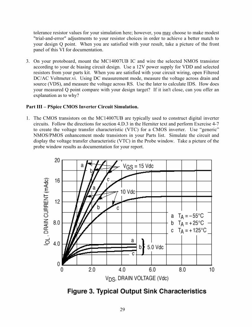
Sheets folder on your workstation.) Figure 3 (attached at the end of this lab for easyreference) in the data sheet for the MC14007UB gives “typical” IDS vs. VDS characteristicsfor the transistors on the chip. Notice that these characteristics vary with temperature overthe rated operating range of the chip. Use the characteristic for VGS = 5 V and TA = 25 °C.Estimate the values of Kn = Kn’(W/L) and VT0 = VTN for VSB = 0, for the NMOS deviceson the chip. Consider using the pinchoff point where VDS = (VGS-VTN) and the saturationregion where IDS = (Kn/2)(VGS-VTN)2 to calculate the two parameter values. Notice that λis very small for these devices and may be approximated as λ = 0 for our estimationpurposes.
5. Open NMOSFETAnalMeas4.vi; examine its front panel, wiring diagram and documentation.Notice that this VI allows you to use a test circuit to directly measure the Kn, VT0, and λparameters of your chosen transistor. Pick one of the NMOS devices on the IC and use thediagram on the lower portion of the front panel of the VI to design a test circuit (as shown onthe VI front panel) for that chosen device on your protoboard. You will use the bench powersupplies and the HP generator for the necessary voltage sources. Leave all gate pins on theunused devices of the IC in an open circuit condition. (Do NOT connect pin 14 to your VDDsource or pin 7 to your VSS source, as indicated in the Schematic Figure. Such a connectionis NOT appropriate for single transistor operation here, and will adversely affect your circuitoperation.) Make sure (if necessary for your transistor choice) to wire a "jumper" betweenthe Base and the Source of the transistor to set VSB = 0 V. Follow the documentation forthis VI, which is conveniently listed with the front panel figure in the appendix of this labmanual, to measure Kn, VT0 and λ for your transistor. Take a picture of your front panel asdocumentation for your report once you are satisfied with your measurements. Note that thisVI uses three simultaneous input channels to obtain necessary circuit voltages. It also uses awhite wire to identify “system ground” for the differential voltage measurements. How doyour measured values for Kn, VT0 and λ compare with the ones calculated in part 4 above?Which set of values will you choose to rely upon for Part II? Why?
Part II – Single Supply DC Biasing Circuit Design and Prototype Construction
1. Open NMOSFETBias3.vi; examine its front panel, wiring diagram and documentation. ThisVI uses the example 4-R bias circuit design done in class as a guide. Assume W/L=10 foryour transistor and your best estimates for VT0, Kn and λ from Part I above. Determinevalues of R1, R2, RD, and RS for a four-resistor biasing network for the selected NMOSdevice on your MC14007UB IC. Design for a Q point (VDS, IDS) of (3.5 V, 5 mA) in thesaturation region of the device. (Adjust the "Gate Margin" parameter to give you 5% resistorvalues close to those available in your parts kit.) Make sure your Q point will be in thesaturation region of the device [VDS > (VGS-VTN) > 0]. Use 12 V as your VDD supplyvoltage.
2. Now open NMOSFET_LL2.vi and examine its front panel, wiring diagram anddocumentation. Notice that this VI will plot the characteristic of your device as well as theload line equation for your biasing circuit. It will also determine the Q point (Q-VDS, Q-IDS) for your device. Enter YOUR device and circuit design data (not the default values).(N.B. that Kn' is entered in A/V2 in this VI.) Note that you will have to choose available 5%
29
tolerance resistor values for your simulation here; however, you may choose to make modest"trial-and-error" adjustments to your resistor choices in order to achieve a better match toyour design Q point. When you are satisfied with your result, take a picture of the frontpanel of this VI for documentation.
3. On your protoboard, mount the MC14007UB IC and wire the selected NMOS transistoraccording to your dc biasing circuit design. Use a 12V power supply for VDD and selectedresistors from your parts kit. When you are satisfied with your circuit wiring, open FilteredDC/AC Voltmeter.vi. Using DC measurement mode, measure the voltage across drain andsource (VDS), and measure the voltage across RS. Use the later to calculate IDS. How doesyour measured Q point compare with your design target? If it isn't close, can you offer anexplanation as to why?
Part III – PSpice CMOS Inverter Circuit Simulation.
1. The CMOS transistors on the MC14007UB are typically used to construct digital invertercircuits. Follow the directions for section 4.D.3 in the Herniter text and perform Exercise 4-7to create the voltage transfer characteristic (VTC) for a CMOS inverter. Use “generic”NMOS/PMOS enhancement mode transistors in your Parts list. Simulate the circuit anddisplay the voltage transfer characteristic (VTC) in the Probe window. Take a picture of theprobe window results as documentation for your report.

30

31
Laboratory 6 – BJT Transistor Characteristics
Objectives: 1) To examine the characteristics of a BJT transistor by means of a mathematicalVI model; 2) to design a single-supply dc biasing circuit for operation of an NPN BJT device inthe forward active region, and 3) to simulate this circuit using PSpice. Upon completion of thislaboratory exercise, you should have a good understanding of BJT transistor characteristics andthe dc biasing of such devices.
Part I – Examining the Electrical Characteristics of BJT Transistors
1. Open LabVIEW and navigate to open the EEE102L Lab_6 folder. Inside you will findthe VIs necessary for this part of the lab: NPNBE.vi, NPNBE_LL.vi, NPNCE.vi,NPNCE_LL.vi, NPNBFISAnalMeas.vi, and Filtered DC/AC Voltmeter.vi.
2. Open NPNBE.vi. Examine its front panel, wiring diagram and documentation. Note thatthe following symbols are used for the NPN BJT transistor model parameters:
3. IS is saturation current; BF is forward (ce) current gain; BR is reverse (ce) current gain; Tis absolute temperature; VCE is collector-emitter voltage; IB is base current and VBE isbase-emitter voltage.
4. A set of default input parameters is present at startup. This parameter set is constructedbased upon data used for NPN BJT device problems in Chapter 4 of your text. Explorehow these parameters affect the IB vs. VBE characteristic of the NPN transistor using thefollowing protocol. In each case, start with the default parameter set and change only theparameter indicated by the protocol. (Use the Reinitialize All to Default command underthe Operate menu.) Describe any significant changes to the characteristic. It is notnecessary to take pictures of the front panel results for each case. Your description of thechanges you observe will be sufficient for your report.
Increase IS by a factor of 10Decrease IS by a factor of 10Increase BF to 200Decrease BF to 20Increase BR to 5Decrease BR to 0.1Increase VCE to 10 VDecrease VCE to 0.1 VIncrease T by 30 °CDecrease T by 30 °C
5. Open NPNCE.vi. Examine its front panel, wiring diagram and documentation. Note thatthe same symbols are used for the NPN BJT transistor model parameters as were used inNPNBE.vi.

32
6. A set of default input parameters is present at startup. This parameter set is constructedbased upon data used for NPN BJT device problems in Chapter 4 of your text. Explorehow these parameters affect the IC vs. VCE characteristic of the NPN transistor using thefollowing protocol. In each case, start with the default parameter set and change only theparameter indicated by the protocol. Describe any significant changes to thecharacteristic. It is not necessary to take pictures of the front panel results for each case.Your description of the changes you observe will be sufficient for your report.
Increase IS by a factor of 10Decrease IS by a factor of 10Increase BF to 200Decrease BF to 20Increase BR to 5Decrease BR to 0.1Increase IB by a factor of 10Decrease IB by a factor of 10Increase T by 30 °CDecrease T by 30 °C
7. Refer to your data sheet on the Motorola 2N2222A NPN BJT transistor. Figure 3(attached at the end of this lab for easy reference) in the data sheet gives “typical” hFE vs.iC characteristics for the transistor. As usual, some different notation is used in the datasheet for the transistor parameters. Here hFE = βF in our textbook notation. Notice thatthese characteristics vary with temperature over the rated range of the collector current.Use the characteristic for T = 25 °C in your design work. Estimate the value of βF forthis transistor for a bias operating Q-point (VCE, IC) = (3.5V, 5 mA). Because weusually buy cheap grades of these transistors for the parts kits, you may find βF to be aslow as 50% of the nominal value found in figure 3. Since it is not very significant inforward active region operation of the transistor, you may assume βR = 1. UseNPNBFISAnalMeas.vi to measure the βF and IS values for your transistor under thespecified bias conditions. (Be sure to read the Documentation window before you begin.)Use the previous two VIs, with these measured BF and IS values, to plot the expected IBvs. VBE and IC vs. VCE characteristics for this transistor. What value would youestimate to be appropriate to use for VBE in your bias circuit design?
Part II – Single Supply DC Biasing Circuit Design and Prototype Construction
1. Use problem 5.87 and Figure 5.39 in your Jaeger text as a design guide. (Note thatproblem 5.87 was done as an example for you in class.) Open NPNBias.vi and read itsdocumentation window. Use it to determine values of R1, R2, RC, and RE for a four-resistor biasing network for the 2N2222A. Design for a Q point (VCE, IC) of (3.5 V, 5mA) in the forward active region of the device. Use 12 V for VCC. Leave C-E Vdrops = 2,but adjust the Base Margin to yield acceptable resistor values. You will have to choosethe nearest 5% resistor values in your parts kit for your actual circuit design. Choosethese now, and use their values in the following circuit verification VIs.
33
2. Open NPNBE_LL.vi and examine its front panel, wiring diagram, and documentation.Notice that this VI will plot the IB vs. VBE characteristic of your device as well as thebase-emitter sub-circuit load line equation for your biasing circuit. It will also determinethe Q point (Q-VBE, Q-IB) for your device. Enter your device and circuit designparameters and RUN the VI to examine your Q point. Is it what you expected for FARoperation of the transistor? Note the Q point value of IB because you will need it forinput in the next design verification VI. Close NPNBE_LL.vi and open NPNCE_LL.vi.Again, examine front panel, wiring diagram and Documentation. This VI will plot the ICvs. VCE characteristic of your device, as well as the collector-emitter sub-circuit loadline equation for your biasing circuit. Together, they determine the Q point (Q-VCE, Q-IC) for your device. Enter your device and circuit design parameters and RUN the VI toverify your Q point design. You may choose to make slight adjustments to your resistorvalues (5% values) to achieve a better match to your design Q point. Take pictures of thefront panels of these two design verification VIs to document your final result.
3. On your protoboard, mount the 2N2222A transistor from your parts kit and wire itaccording to your dc biasing circuit design. Use a 12 V power supply as your protoboardVCC supply voltage.
4. When you are satisfied with your circuit wiring, open Filtered DC/AC Voltmeter.vi.Using DC measurement mode, measure the voltage across collector and emitter (VCE),and measure the voltage across RC. Use the later to calculate IC. How does yourmeasured Q point compare with your design target? If it’s not too close, measure VBE.Is it what you expected for your design?
Part III – PSpice Single Supply DC Biasing Circuit Simulation.
1. Open PSpice Capture and construct the schematic of your 2N2222A transistor biasingcircuit. Simulate the circuit and display VBE, VCE, and IC to confirm the Q point. Takea picture of the schematic with the I and V data displayed as documentation of yourresults.
Note that a formal laboratory report on this lab should be included with the one for Lab 5.
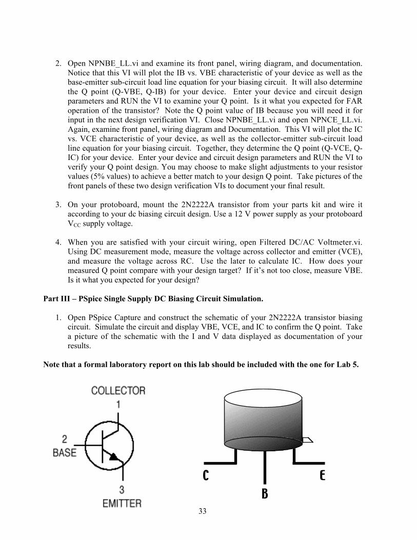
EB
C

34
2N2222A NPN Bipolar Junction Transistor – Forward (ce) Current Gain as a function ofCollector Current

35
Laboratory 7 – Common-Emitter Amplifier Design
Objectives: 1) To design a high voltage gain, common-emitter amplifier using an NPN BJTtransistor and a single-supply dc biasing circuit, 2) to construct a prototype of the design and testit for ac voltage gain, and 3) to simulate this circuit using PSpice. Upon completion of thislaboratory exercise, you should have a good understanding of common-emitter amplifier designand requirements for the dc biasing of such circuits.
Part I – Circuit Design and Verification Using LabVIEW
1. Design a common-emitter amplifier that will employ a 2N2222A NPN BJT as the activedevice. Your amplifier should have an ac voltage gain (|AV| ≥ 100) at a frequency (f =100 Hz) with load resistance R3 = 100 KΩ. Your design will employ an ac voltagesource (vs) with RS = 15 Ω. Your circuit design should use appropriate availablecoupling capacitors (C1, C2, and C3) and appropriate dc biasing resistors (R1, R2, and RC,RE) from your parts kit. Use a 12V power supply as your VCC supply voltage. Note thatyou will have to determine appropriate dc bias values of VCE and IC for your amplifier.What factors must you consider in determining them?
2. On your VI workstation, open LabVIEW and navigate to the EEE102L Lab_7 folder.Inside are all the VIs you will need for this laboratory. Open NPNCEBias.vi. Althoughyou have seen this VI before in Lab 6, examine its front panel, wiring diagram, anddocumentation once again, if necessary. Note that the ac model parameters for thetransistor are added as a calculation to this bias circuit designer. β and IS should be set tosimulate what you have measured in Lab 6 for your 2N2222A transistor. Enter theabsolute temperature (T) of the room (check the Fluke RTD by the door to RVR-5017A),power supply voltage (VCC) and your desired dc bias values for VCE and IC. RUN theVI to calculate your dc bias circuit design values. You may adjust C-E Vdrops and BaseMargin to yield reasonable 5% resistor values.
3. Close NPNCEBias.vi and open both NPNBE_LL.vi and NPNCE_LL.vi. You have alsoseen these VIs before in Lab 6. Examine the documentation window again, if necessary.Use these VIs to enter the 5% resistor design values for your dc biasing circuit, and RUNthe VIs to verify the dc Q points of your design. Take pictures of the front panels ofthese VIs to document your results.
4. Close these two VIs and open CEAmpAnal.vi. This one you have not seen before.Examine its front panel, wiring diagram, and documentation window to learn about itsfunctions and operation. The following circuit design parameters are required as inputsfor this VI:
Rs is the equivalent voltage source resistanceVsp is the peak input source voltageC1, C2, and C3 are the ac coupling and by-pass capacitorsFrequency is the frequency of the input signal in HzR1, R2, R3, and Rc are the relevant bias circuit and ac load resistances
36
rπ , gm, and ro are the respective small-signal ac input resistance,transconductance, and output resistance of the transistor at the design Q-point.
5. Enter the appropriate input parameters for your common-emitter amplifier circuit design.Consider the size of the coupling and bypass capacitors that you will need. Note thatpeak input signal amplitude (Vsp) will be 5 mV. RUN the VI to calculate the expectedpeak ac output voltage (Vop) and ac voltage gain (Av). Notice that a representation ofthe expected ac output voltage is displayed on the VI waveform graph. If your gain is notsufficient, consider redesigning the circuit with a different value of IC. When you aresatisfied with your design and its verification by the LabVIEW VIs, construct the circuiton your protoboard.
Part II – Common-Emitter Amplifier Prototype Construction and Testing
1. On your protoboard, mount the 2N2222A transistor and wire the transistor andappropriate passive components according to your common-emitter amplifier circuitdesign. Using a signal generator set to deliver a 20 V p-p sinusoidal output signal at afrequency of 100 Hz, construct the resistive voltage divider circuit shown in Figure 1. Itwill deliver a Thevenin equivalent sinusoidal voltage (vs) of approximately 5 mV peakamplitude to C1 through an equivalent source resistance (RS) of 15 Ω.
2. When you are satisfied with your circuit wiring, open Filtered DC/AC Voltmeter.vi.Using AC measurement mode, RUN the VI, measure the voltage (vo(t)) across loadresistor R3, and calculate the ac voltage gain (AV). How do these two compare with yourdesign values? Take a picture of the front panel of this VI to document your results.
Part III – PSpice Common-Emitter Amplifier Simulation.
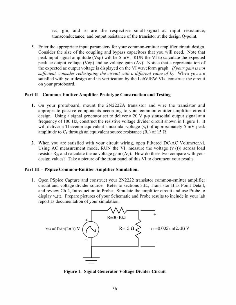
1. Open PSpice Capture and construct your 2N2222 transistor common-emitter amplifiercircuit and voltage divider source. Refer to sections 3.E., Transistor Bias Point Detail,and review Ch 2, Introduction to Probe. Simulate the amplifier circuit and use Probe todisplay vo(t). Prepare pictures of your Schematic and Probe results to include in your labreport as documentation of your simulation.
Figure 1. Signal Generator Voltage Divider Circuit
R=15 Ω
R=30 KΩ
vs =0.005sin(2πft) V
+
--
+
vss =10sin(2πft) V

37
Laboratory 8 – OP Amp Instrumentation Amplifiers and First Order Filters
Objectives: 1) To design a high voltage gain instrumentation amplifier using the Burr BrownINA118 IC and to design a cascaded first order bandpass filter using two LM741 operationalamplifiers; 2) to construct a prototype of the design and test it for overall ac voltage gain andCMRR, and examine its I/O impedance, and 3) to simulate this circuit using PSpice. Uponcompletion of this laboratory exercise, you should have a good understanding of instrumentationamplifier/filter design and the electrical characteristics of such circuits.
Pre-laboratory preparation: Inspect the data sheet for the Burr Brown INA118 in the EEE102L Data Sheets folder on your workstation. Note particularly the circuit design of the IC andhow its differential gain is determined by selection of a single external circuit component. Thispdf file may be copied to a storage device and printed outside of the lab if you desire. Compareits circuit with the example in figure 11.12 in your text. Similarly, review the data sheet for theLM741 Op Amp in the Data Sheets folder on the workstation. Note that you will need two 9 Valkaline batteries with battery clips to construct ± 9 V power supplies to power your circuits inthis laboratory.
Part I – Circuit Design and Verification Using LabVIEW
1. Determine appropriate external components for use with the INA118 to achieve aninstrumentation amplifier with differential voltage gain of 1000 at a frequency of 100 Hz.
GEN V DIV INA118 VO- -+ +µΑ741 µΑ741
Amplifier/Bandpass Filter Block Diagram
2. Consider the Low-Pass Filter description in section 11.3.7 in the Jaeger text, along withdesign information presented in class, and determine appropriate external components foruse with a LM741 op amp to construct a high-pass first order filter with a -3db cutofffrequency of 10 Hz and a voltage gain of 1 in the "high-pass" frequency region.
3. Similarly, determine appropriate external components for use with a second LM741 opamp to construct a low-pass first order filter with a -3dB cutoff frequency of 1000 Hz anda voltage gain of 1 in the 'low-pass" frequency region. Remember that these circuits willbe using components from your parts kit, so choose available R and C values for yourdesigns that will achieve the desired specifications.
4. Open LabVIEW on your workstation and navigate to Amp/Filter.vi in the EEE102LLab_8 folder. Open this VI, read its documentation, and enter the data required for this
38
VI to verify your design values at a frequency of 100 Hz. RUN the VI and compare bothpeak output voltage and gain to your predicted design values. Repeat this for frequenciesof 10 Hz and 1000 Hz. If your design checks out ok, take pictures of the front panel foreach of the 3 frequencies as documentation for your report and proceed to Part II below.If it doesn't check out, go back and re-analyze your design.
Part II – Instrumentation Amplifier/Bandpass Filter Prototype Construction and Testing
1. At one end of your protoboard, mount the INA118 and wire it according to your design.Make sure both battery power supplies are connected as required. Using a signalgenerator set to deliver a 20 V p-p sinusoidal output signal at a frequency of 100 Hz,construct the resistive voltage divider circuit shown in Figure 1 below. It should deliver aThevenin equivalent sinusoidal voltage (vs) of approximately 5 mV peak amplitudethrough an equivalent source resistance (RS) of 15 Ω to the differential input pins of theINA118. Note that this circuit is slightly different from the one used in the previouslaboratory in that the voltage (vs) is not referenced directly to "ground". Make sure youhave a common reference ground in your circuit. The ground side of the HP generator,pin 5 (ref) of the INA118, and the ground terminal of your battery supplies, must all beconnected together (common ground).
2. When you are satisfied with your wiring, connect the instrumentation amplifier inputsacross the 15 Ω resistor of the voltage divider. Open Filtered DC/AC Voltmeter.vi.Using AC measurement mode, RUN the VI and measure the voltage at the output pin ofthe IC. Calculate the ac voltage gain (AV). How does it compare with your design value?Take a picture of the front panel of this VI to document your results.
3. Because this instrumentation amplifier has such a high differential input impedance, it isalmost impossible to measure it using general-purpose test instruments such as we havein the laboratory. In order to get an impression for how large this input impedance reallyis, insert a 51 KΩ resistor from your parts kit in series with the + input of theinstrumentation amplifier. Again, measure the voltage at the output pin of the IC. Doesthe 51 KΩ resistor make any difference? Consider the high input impedance of theINA118 circuit design and explain why.
4. Remove the 51 kΩ resistor and reconnect the + input of the instrumentation amplifierdirectly to the voltage divider. Now place a 2.2 KΩ resistor between the output pin of theIC and ground (output load resistor). Measure the voltage across the resistor andcompare it to the "open circuit" output voltage. Is there a difference? Try this again witha 1 KΩ resistor. If there is still no difference, try a 510 Ω resistor. What do thesemeasurements indicate about the output current limit for your IC? What is the minimumload impedance you should design for if you expect to achieve the desired 10 V peak-to-peak output voltage swing?
5. Remove the load resistor. Disconnect the signal generator from the voltage divider andconnect BOTH the + and - inputs of the instrumentation amplifier directly to the + outputterminal of the signal generator to produce a “common mode” input signal. Set the

39
generator to produce a 5 V p-p sine wave. Again, measure the voltage at the output pinof the IC. (Note you may have to edit the voltage scale after recording in order tomagnify the signal and measure the small common mode output voltage. Ignore any"spike" noise that may be present and measure (estimate) the p-p amplitude of the 100 Hzsinusoidal signal.) Determine the common mode gain for your amplifier. Calculate thecommon mode rejection ratio in decibels (CMRR in dB). When you are finished, returnyour input connections to the voltage divider as before, and reset your signal generatoramplitude to 20 V p-p.
6. Next to the INA118 on your protoboard, mount one LM741 op amp and wire it accordingto your high-pass filter design. Connect the filter input to the instrumentation amplifieroutput, and use the Filtered DC/AC Voltmeter.vi to measure the filter output voltage.How does it compare to the instrumentation amplifier output voltage measured in part 2above? Now change the signal generator frequency to 10 Hz and measure the filteroutput voltage again. Is the amplitude of the output voltage reduced by -3dB (a factor of.707) at this frequency as predicted by your design? Explain.
7. Right next to the high-pass filter mount another LM741 op amp and wire it according toyour low-pass filter design. Measure the output voltage of the low-pass filter at 100 Hz.Is it what you expected? Change the signal generator to a frequency of 1000 Hz andmeasure the low-pass filter output voltage. Is the amplitude reduced by -3dB at thisfrequency as predicted by your design? Explain. Measure the output voltage of yourlow-pass filter at 100 Hz. Nominally, it should be 5 V peak. Is it greater or less than youexpected? What instrumentation amplifier and/or filter circuit modifications could youmake to achieve an output voltage closer to this design expectation? For reportdocumentation, take pictures of the front panel of your VI that show your completedcircuit output at frequencies of 10 Hz, 100 Hz, and 1000 Hz.
Part III – PSpice Filter Simulation
1. Open PSpice Capture and construct the bandpass filter section (only) of your circuit usingLM741 op-amps from the parts library. Use a VSIN sine wave voltage source (at 100 Hzand 5 mV peak amplitude) from the Parts library as input to your filter. Set up asimulation to examine the circuit using an AC frequency sweep from 5 Hz to 5 kHz. UseProbe to display the final output voltage vo amplitude as a function of frequency for thefrequency sweep from 5Hz to 5 kHz. Prepare pictures of your Schematic and Probewindows to include in your lab report as documentation of your results.

40
Figure 1. Signal Generator Voltage Divider Circuit
Note that a formal laboratory report on this lab, along with the one for Lab 7, is due onyour lab day in the 16th week (finals week) of the semester.
R=15 Ω
R=15 KΩ
vs =0.005sin(2πft) V
+
--
+
vss =10sin(2πft) V
R=15 KΩ

41
APPENDIX
1. TAKING PICTURES OF THE ACTIVE WINDOW ONMACINTOSH WORKSTATIONS
2. EEE 102 L VIRTUAL INSTRUMENT DOCUMENTATION
3. NATIONAL INSTRUMENTS 6024E DAQ BOARD I/O PINCONNECTIONS

42
Procedure for taking a "Picture" of the active window onMacintosh workstations
1. Make sure the window is active by executing a single mouse click somewhere inside thewindow.
2. Set the caps lock key and press Shift 4 (three keys) simultaneously. The mouse pointerwill change to a camera shutter.
3. Click the mouse in the active window. You will hear the sound of a camera shutter fromyour workstation.
4. The "picture" of the window will be found as a document labeled Picture #, where # isthe number of the picture taken. That document will be located inside the hard drivepartition (icon) on the desktop.
5. If the hard drive icon is obscured on your desktop, you can get to the hard drive partitionmost easily by executing a mouse click on the program icon in the upper right-handcorner of the Macintosh menu bar, and selecting Finder. Repeat this mouse click andselect Hide Others from the sub-menu. Then double-click on the hard drive icon thatshould now be visible just below the menu bar on the right side of the desktop. You'llfind the Picture # document in the window that opens.
6. These documents are saved on the Macintosh in a .pict format. This format is easilyhandled by word processors, and you can usually insert these pictures directly into a wordprocessing document. Specifically, Microsoft Word can insert these files directly into adocument file using the Insert/Picture/From File command, or simply by dragging thepicture document into the open word document page. Save your desired Word(preferred) or picture files to your personal storage device or account.
7. Please remember to drag all picture files into the trash and Empty the trash (find theEmpty Trash command under the Special menu) before you finish your session on theworkstation.
EEE 102L Virtual Instrument Documentation
A/DResCheck2.viThis is a high precision DC/AC voltmeter that incorporates a forth-order Butterworth anti-aliasing filter to provide high noise immunity and high measurement precision in DC mode.Click the RUN (arrow) button to start measuring continuously. Monitor voltage stability usingthe monitor graph. Click the STOP button on the VI front panel to stop (red) and hold the dataon the graph for the current sampling period. Click the STOP button again (white) to reset theVI for the next continuous RUN. (Note: You may take single voltage samples (one sampling
43
period) by clicking RUN with the STOP button depressed (red).) Click and drag the red and bluecursors on the waveform graph to measure time (X) in seconds and amplitude (Y) in volts.There are two AC modes of recording: RMS reading and Peak-to-Peak reading that are set bythe AC Mode switch when the AC/DC slide switch is in the AC position.
This VI is configured for measuring National Instruments 6024E board A/D converter amplituderesolution using a variety of measurement protocols. The Boolean Conversion display recordsthe binary output (12-bit) of the converter for the measured analog voltage.
Alias3.viThis VI is designed to illustrate the phenomenon of aliasing using a 100 Hz sine wave signal asinput to channel 0. Click on the RUN button in the menu bar to start the VI. Click on the STOPbutton on the front panel (NOT the menu bar) to hold the next record. Click this button toRESET the VI before you RUN it again.
Waveform 1 is sampled at a fixed rate of fs = 1000 samples/s. You may switch Waveform 2 infive steps between sampling frequencies of 125 samples/s and 250 samples/s using the SamplingFrequency switch. LOOK AT BOTH THE SHAPE AND THE APPARENT FREQUENCY OFTHE WAVEFORM 2 SINE WAVES AS COMPARED TO WAVEFORM 1. You can measurewaveform periods using the cursors. Frequency = 1/period. Click and drag the center of a cursorwith the mouse to position it on the waveform graph. X is time in seconds and Y is amplitude involts.
GDAnal2.viThis Conditional Trigger Data Acquisition VI acquires specified data from one or more analoginput channels. A hardware clock is used to control the acquisition rate for fast and accuratetiming. The data is stored in an intermediate memory buffer after it is acquired from the analoginput channels. The VI retrieves the data that matches the trigger condition, displays it and stopsthe acquisition.
The VI has been configured to measure Rise Time, Slew Rate, and Delay Time for acquiredlogic gate waveforms on two channels, (0 and 1), and to use a Property Node to automaticallyposition the waveform graph cursors. The 10% and 90% points on the output waveform, andthe 50% points (TI and TO) on both waveforms are displayed for reference.
WavAnal3.viThis VI allows you to record both time and frequency (amplitude spectrum) domain signalsusing channel 0. The digital sampling rate is designed to accommodate a signal with afundamental frequency on the order of 100 Hz. Clicking the red STOP button on the front panel(NOT the menu bar) will hold the data from the next sampling period. Click RESET then RUN(arrow) to resume continuous recording. Clicking RUN in RESET mode will allow you torecord single records. You can move the cursors by clicking and dragging with the mouse inorder to make detailed measurements of amplitude (Y) in volts in either the time or frequencydomain (X). Pushing the Filter button will cause the signal to be sharply lowpass filtered with a

44
passband from 0 - fc Hz., where the cutoff frequency, fc, is set using the slide switch inincrements of 200 Hz from 0 to 1000 Hz.
Diode Current Analyzer.viThis VI allows you to simply solve the "diode equation" under a variety of input conditions.You can easily explore the effect of your input choices on the diode current. Be sure to checkout the wiring Diagram to see how this VI is implemented. Notice that saturation current (Is) hasbeen corrected for temperature variation to make the calculation of diode current even morerealistic. Use of this VI simply requires a known saturation current (Isref) at a known referencetemperature (Tref) for the diode to be modeled . The effects of temperature (T), non-idealityfactor (n) and diode voltage (VD) on diode current (ID) can be observed. Edit the input data asrequired and click on the RUN (arrow) button to operate the VI.
Diode Graph.viThis VI allows you to create a convenient graph of the forward ID vs. VD characteristic of adiode. You can use measurement cursors, along with appropriate expansions of the axis scales,to make desired measurements of this characteristic. The set of diode voltages (VD) specifiedfor the diode problem in lab 3 have been entered as default values in the graph array. Use thetext tool to enter the corresponding ID array values obtained from the Diode Current Analyzer.vi.Then RUN the VI to see your graph. You can "zoom" in on a data point on the graph by simplyediting the axis limit values with the text tool. You can perform measurements using the red andgreen cursors.
Diode Junction Analyzer.viThis VI is designed to allow you to explore the diode junction conditions that will produce"breakdown" under reverse voltage bias. You can change the properties of the diode as inputvariables and explore the consequences of those changes on the breakdown voltage, depletionzone width, and junction capacitance. Be sure to look at the Wiring Diagram to appreciate thecritical formulas that govern these phenomena.
Have fun!
Filtered DC/AC Voltmeter.viThis is a high precision DC/AC voltmeter that incorporates a forth-order Butterworth anti-aliasing filter to provide high noise immunity and high measurement precision in DC mode.Click the RUN button to start measuring continuously. Monitor voltage stability using themonitor graph. Click the STOP button on the VI front panel to stop (red). Click the STOPbutton again (white) to reset the VI for the next continuous RUN. (Note: You may take single 1second voltage samples by clicking RUN with the STOP button depressed (red).) There are twoAC modes, RMS reading and Peak-to-Peak reading that are set by the AC Mode switch when theAC/DC switch is in the AC position. Cursors can be dragged to make differential measurementson the monitor graph.
45
Rectifier Supply.viThis VI is designed to allow the user to input specified parameters for a simple half wave or fullwave rectified power supply. It then uses a formula node to calculate the required componentparameters for the design after the RUN button is pressed. Note that the Constant Voltage Drop(CVD) for the diode(s) used must be estimated. For the W005G Bridge Rectifier used in the lab,a CVD = 1.1V is a good estimate for operation at a peak current on the order of 100 mA.
NMOSFET.viThis NMOS FET analyzer VI is designed to simulate the IDS vs. VDS characteristic of anenhancement mode (VT0 > O) or depletion mode (VT0 < 0) NMOS field effect transistor. Themodeling includes both channel length modulation effects and body voltage effects. It alsocalculates the VDS at "pinchoff". Enter the appropriate input parameters for the device and pressthe RUN button.
NMOSFETAnalMeas4.viThis VI is designed to allow the user to input three channels of specified voltage measurementsfrom the NMOS transistor test circuit shown in the diagram below the front panel, and tocalculate the threshold voltage (VT0), transconductance (Kn) and channel width modulation(lambda) of the transistor. It requires two RUN cycles to calculate these parameters. In the firstRUN cycle, the VDS vs. IDS characteristic at measured VGS will be graphed. Note that theVTO, Kn and lambda output parameters will not necessarily be accurate at this point. The usermust then determine the "pinchoff point" (VDS, IDS at pinchoff) from the graph (drag thecursor), and input them under "Graph Measurement" on the panel. Clicking on the RUN arrow asecond time will calculate accurate VTO and Kn values for the device.
Required Input Voltages: Channel 0 -- VGS; Channel 1 -- VDS; Channel 2 -- VRD (voltageacross resistor RD).
Required Voltage Sources: VSS -- 12 V DC; VDD -- 5 + 5 sin 2(pi)t V (5 V peak amplitudesine wave with 5 V DC offset and frequency of 1 Hz). Special note: Because of maximumvoltage output limitations, in order to produce VDD with the HP Signal Generator, you will haveto refrain from using the 50-ohm feedthrough connector and set the generator to 2.5 V DC offset,and 5 V PP amplitude sine wave at a frequency of 1 Hz. Remember, without the 50-ohmfeedthrough connector, all offset and peak-to-peak amplitude readings are effectively doubled atthe output.
Required Resistances: R1 = 100 K ohms R2 = 200 K ohms; RD = 1 K ohms.
NMOSFETBias3.viThis VI is designed to allow the user to input specified parameters for design of a four-resistor dcbiasing circuit for an NMOS FET. It then uses a formula node to calculate the requiredcomponent parameters for the design of the biasing circuit, after the RUN button is pressed.Default parameters are from the instructor’s personal NMOSFET circuit. Note that Gate Marginis the selected source-to-ground voltage (difference between gate-to-ground and gate-to-source

46
voltages). Gate Fraction is the ratio of gate-to-ground voltage/VDD. Other parameters are thosecommonly associated with NMOS devices and the biasing circuit.
NMOSFET_LL2.viThis NMOS FET analyzer VI is designed to simulate the IDS vs. VDS characteristic of anenhancement mode (VT0 > O) or depletion mode (VT0 < 0) NMOS field effect transistor. Themodeling includes both channel length modulation effects and body voltage effects. DC biasingusing a four-resistor, single supply circuit sets the Q point for the device in the saturation region.The circuit load line is calculated for verification of the Q point. Q point calculation is preciselyvalid only for zero channel length modulation; however small values of lambda may beaccommodated with good result.
NPNBE.viThis NPN BJT analyzer VI is designed to simulate the IB vs. VBE (first quadrant) characteristicof an NPN transistor. The modeling is based upon a modified Gummel-Poon description of thetransistor. IS is the saturation current at temperature T, BF is the forward (ce) current gain, BRis the reverse (ce) current gain, T is absolute temperature, IB is base current, VCE is thecollector-emitter voltage, and VBE is the base-emitter voltage. Note also that there is NOcorrection of IS in this model for changes in temperature. Input the appropriate parameters andpress the RUN button.
NPNCE.viThis NPN BJT analyzer VI is designed to simulate the IC vs VCE characteristic in the firstquadrant of an NPN transistor. The modeling is based upon the Gummel-Poon description of thetransistor, but does not include the Early effect. IS is saturation current, BF is forward (ce)current gain, BR is reverse (ce) current gain, IB is base current, T is absolute temperature, VCEis collector-emitter voltage, IC is collector current. Note that IS is NOT corrected for changes intemperature T.
NPNBFISAnalMeas.viThis VI is designed to allow the user to input specified and measured parameters from the NPNBJT transistor circuit shown, and calculate the BF and IS of the transistor. It uses a formula nodeto calculate the required parameters after the RUN button is pressed. Parameters follow standarddefinitions for the NPN BJT. Default parameters are from the instructors personal 2N2222ABJT. Channel 0 is designed to measure VBE in the circuit, and channel 1 is designed to measureVCE. Assumptions are that the biasing setup operates the transistor in the forward active regionand that VA (Early Voltage) is very large, so corrections to BF can be neglected. The"Betometer" provides a graphic display of forward current gain.
NPNBias.viThis VI is designed to allow the user to input specified parameters for design of a four-resistor dcbias circuit using an NPN BJT. It then uses a formula node to calculate the required componentparameters for the design after the RUN button is pressed. C-E V Drops is a parameter that setsthe distribution of voltage drop between RC and RE. A factor of 2 divides the drop evenly; a

47
factor of 3 divides the drop 1/3 to RC and 2/3 to RE, etc. Base Margin sets the ratio of Collectorto Base bias supply current. A default value of 5 is used to be consistent with the text. LargerBase Margin values give more power-efficient circuit performance. f is the base voltage dividerfraction. r is the (BF+1)RE/REQ ratio and should be >> 1. If it isn't, reducing the Base Marginwill help. Other parameters follow standard definitions for the NPN BJT and biasing circuit.Default parameters are those from problem 5.87 in the text.
NPNBE_LL.viThis Q-point analyzer VI is designed to simulate the IB vs VBE characteristic of an NPNtransistor, and calculate the Q point (Q-VBE, Q-IB) for forward active region operation in afour-resistor, single voltage supply dc biasing circuit. The VI calculates the BE circuit load lineequation and plots it to help you graphically visualize the Q point solution. IS is the saturationcurrent at temperature T, BF is the forward (ce) current gain of the transistor, BR is the reverse(ce) current gain, T is absolute temperature, RE, R1, and R2 are the relevant biasing circuitresistances, VCC is the supply voltage, VCEQ is collector-emitter Q-point voltage, and ICEQ isthe Q-point collector current. The default parameters correspond to the solution to problem 5.87in your text. Note also that there is NO correction of IS in this model for changes in temperature.
NPNCE_LL.viThis Q-point analyzer VI is designed to simulate the IC vs. VCE characteristic of an NPNtransistor, and calculates the Q point (Q-VCE, Q-IC) for forward active region operation in afour-resistor, single voltage supply dc biasing circuit. The VI calculates the CE circuit load lineequation and plots it to help you graphically visualize the Q point solution. BF is the forward(ce) current gain of the transistor, IS is the saturation current, BR is the reverse (ce) current gain(default 1.0), T is absolute temperature, VCC is the supply voltage, R1, R2, RC, and RE are thebiasing circuit resistances. VCE is collector-emitter voltage, IC is collector current, and Q-VCEand Q-IC are the calculated VCE and IC Q point solution set. The default parameters correspondto the solution to problem 5.87 in your text.
CEAmpAnal.viThis VI is designed to allow the user to input specified parameters for small-signal ac analysis ofa CE BJT amplifier circuit. It uses a formula node to calculate the peak output voltage and acvoltage gain parameters for the design when the RUN button is pressed. It also displays arepresentation of the sinusoidal output voltage as a function of time.
Input parameters:Rs is the equivalent voltage source resistance; Vsp is the peak input source voltage; C1 is theinput ac coupling capacitance; C2 is the emitter bypass capacitor and C3 is the output couplingcapacitor; frequency is the frequency of the input signal in Hz; R1, R2, R3, RE and RC are therelevant bias circuit and ac load resistances; rp, gm, and ro are the respective small-signal acinput resistance, transconductance, and output resistance of the transistor at the design Q-point.(See Circuit Diagram below the front panel.)
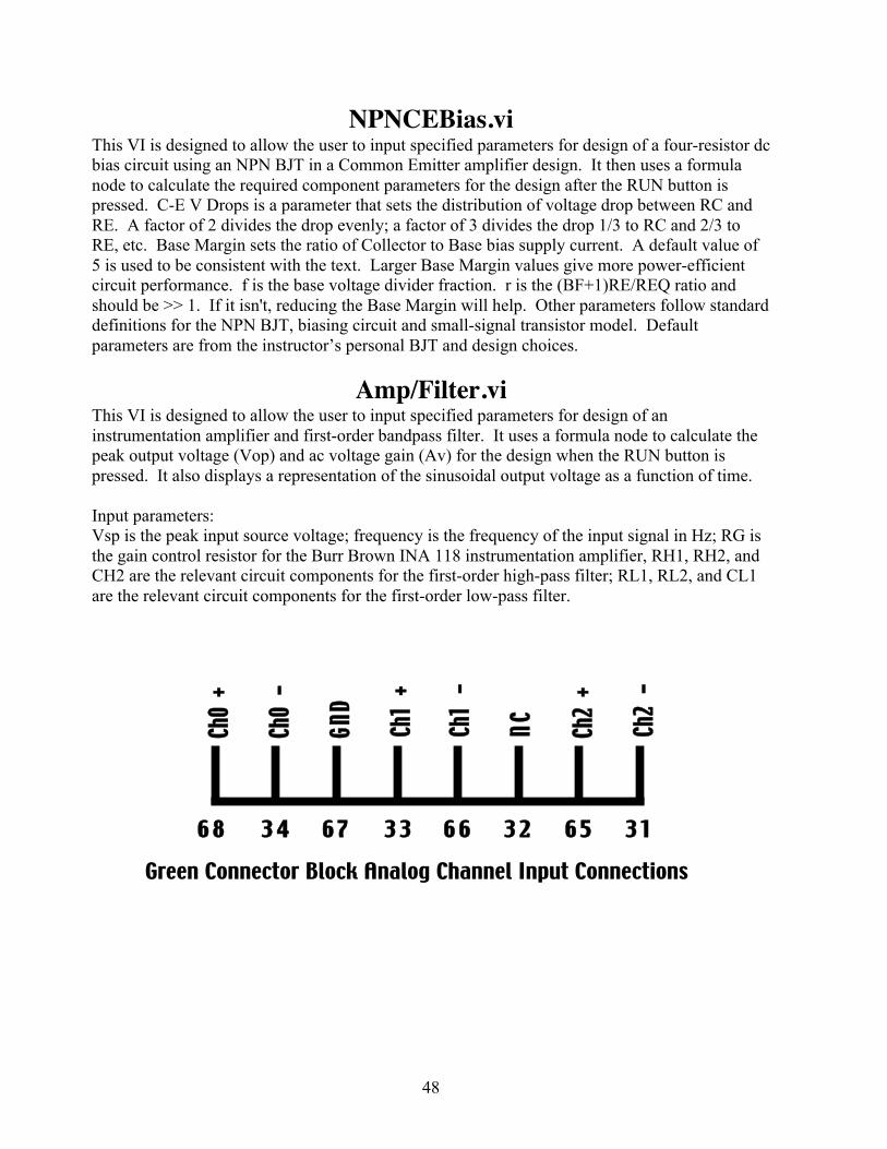
48
NPNCEBias.viThis VI is designed to allow the user to input specified parameters for design of a four-resistor dcbias circuit using an NPN BJT in a Common Emitter amplifier design. It then uses a formulanode to calculate the required component parameters for the design after the RUN button ispressed. C-E V Drops is a parameter that sets the distribution of voltage drop between RC andRE. A factor of 2 divides the drop evenly; a factor of 3 divides the drop 1/3 to RC and 2/3 toRE, etc. Base Margin sets the ratio of Collector to Base bias supply current. A default value of5 is used to be consistent with the text. Larger Base Margin values give more power-efficientcircuit performance. f is the base voltage divider fraction. r is the (BF+1)RE/REQ ratio andshould be >> 1. If it isn't, reducing the Base Margin will help. Other parameters follow standarddefinitions for the NPN BJT, biasing circuit and small-signal transistor model. Defaultparameters are from the instructor’s personal BJT and design choices.
Amp/Filter.viThis VI is designed to allow the user to input specified parameters for design of aninstrumentation amplifier and first-order bandpass filter. It uses a formula node to calculate thepeak output voltage (Vop) and ac voltage gain (Av) for the design when the RUN button ispressed. It also displays a representation of the sinusoidal output voltage as a function of time.
Input parameters:Vsp is the peak input source voltage; frequency is the frequency of the input signal in Hz; RG isthe gain control resistor for the Burr Brown INA 118 instrumentation amplifier, RH1, RH2, andCH2 are the relevant circuit components for the first-order high-pass filter; RL1, RL2, and CL1are the relevant circuit components for the first-order low-pass filter.
6 8 3 4 6 7 3 3 6 6 3 2 6 5 3 1
Ch0
+
Ch0
-
Ch1
-
Ch1
+
Ch2
+
Ch2
-
GND
NC
Green Connector Block Analog Channel Input Connections