csnsm fev boards status n. seguin-moreau on behalf of stéphane callier, dominique cuisy, julien...
TRANSCRIPT

CSNSM
FEV Boards status
N. Seguin-Moreau on behalf ofStéphane Callier, Dominique Cuisy, Julien
Fleury

DESY 2010, 5 July 2
Reminder : FEV5 with HARDROC1
18cm
18cm
1296 channels. 8 HARDROC (512 channels equipped)
PCBWAFER
HARDROC
HARDROC1: 240 staggered pads
FEV5: too difficult to manufacture, bad quality of the bonding pads

DESY 2010, 5 July 3
FEV7-CIP: with SPIROC2 in TQFP208
• 2 boards are equipped with 1 chip and 1 PCB equipped with 4 chips
• On the board access to :– Analogue Output– DAC and Bandgap Output
• On the connector, access to :– Every common digital line
• Easy to manufacture
• Interconnexions tests: perofmed successfully (P. Cornebise)
• Perfect for DIF debug
• Fits the H structure

DESY 2010, 5 July 4
FEV7-COB: with SPIROC2 COB
• Front End Board using Chip-On-Board (spiroc2=208 pads)
• Nearly Identical to Chip-In-Package FEV7– Schematics identical– Same number of channels– Same pinout on Adapter
Board/Slab Connector
• Except :– Pads connections to chip
pins– Position of Wafer on the
bottom side– Thickness: thinner to comply
with H alveolar structure

DESY 2010, 5 July 5
Pile-upTOP GND + Input chip signalC2 horizontal routing + DVDD + GNDC3 AVDDC4 GND + vertical routingC5 GND (pads signal shielding)C6 pads routingC7 GND (pads shielding)BOT PADS
FEV7 COB: Chip Embedding
4 drilling sequences :- Laser C7-C8 120µ filled- Laser C6-C7 120µ- Mechanical C1-C7 200µ- Mechanical C1-C8 (for PCB fastening)
PCB Thickness ~781µm
Resin (300µm)for chip protection

DESY 2010, 5 July 6
FEV7-COB Report
• Plated Through Hole Cross Section :
• 2 Manufacturers :– Elvia : 6 PCB received (2 batchs)– Protechno : 6 PCB received (2 batchs)
• Mechanical report :– Manufacturers Measurements :
• 0.83mm Elvia, 0.93 Protechno– LLR Measurements :
• between 0.83 & 0.94 for both boards

DESY 2010, 5 July 7
FEV7-COB: BONDING
– We have an official agreement with CERN for free bonding • Reminder : 1830 € for 2 boards (8 chips -> ~800 wires to bound)
– Still resin pb for chip protection: to be solved• We have to keep a low thickness of the cabled PCBs
• 2 PCB FEV7-COB fully bonded

DESY 2010, 5 July 8
FEV7- COB2:
Pile-up: 10 layers Top cover layer connected to GNDC2 GND + Input chip signalC3 horizontal routing + DVDD + GNDC4 AVDDC5 GND + vertical routingC6 GND (pads signal shielding)C7 pads routingC8 GND (pads shielding)BOT PADS
4 drilling sequences :- Laser C8-C9 120µ filled- Laser C7-C8 120µ- Mechanical C2-C8 200µ- Mechanical C1-C9 (for PCB fastening)
PCB Thickness 1100 µm
Drilling sequence
• No solder mask on TOP layer• Fit the H structure, access to the analog signals• TOP electrically linked to GND=> too difficult to manufacture (same pbs as for
FEV5) => FEV8

DESY 2010, 5 July 9
FEV8: Chip Embedding
Pile-up: 8 layers +FLOATING Mechanical interposer on the TOPC1 GND + Input chip signalC2 horizontal routing + DVDD + GNDC3 AVDDC4 GND + vertical routingC5 GND (pads signal shielding)C6 pads routingC7 GND (pads shielding)C8 PADS
FEV 8
4 drilling sequences :- Laser C8-C9 120µ filled- Laser C7-C8 120µ- Mechanical C2-C8 200µ- Mechanical C1-C9 (for PCB fastening)
PCB Thickness 1100 µm
Drilling sequence removed
SKIROC2
7.223 x 8.644mm
• PCB currently under design• Fits the H structure, access to the analog signals• Currently under design in collaboration with our Korean colleagues• Will be equipped with SKIROC2 chips

DESY 2010, 5 July 10
SKIROC2 (1)
• 64 inputs, 1/2 Mip to 2500 Mip (keeping the same gain)• Analogue signal-to-noise ratio : 17 (1500 e- noise for 1 MIP)

DESY 2010, 5 July 11
SKIROC2 (2)• Submitted in the prod run
(March 2010): – 1200 SKIROC2– Wafers sent this week to
I2A technology (Fremont-USA) for thinning, dicing and packaging)
• 250 pads– 3 NC– 17 for test purpose only
• A few samples will be packaged in a ceramic 240 pins package to be tested easily on a testboard
• First tests foreseen next October

DESY 2010, 5 July 12
Summary
• No manufacturing critical issue with – FEV7-CIP– FEV7-COB
• No bonding issue with FEV7-COB for both manufacturers
• Next FEV8 will have 16 Skiroc2 chips– 1024 channels on 180 mm x 180 mm board– Our Korean colleagues (Sung Kyun Kwan University) should
take in charge half of the next FEV8 production
• First tests of packaged SKIROC2 expected in October

CSNSM
BACKUP SLIDES

DESY 2010, 5 July 14
FEV7 Board(s)
5 mm x 5 mm pads size180 mm x 180 mm wafer size-> 324 pads on a ¼ board
use of SPIROC2 (36 ch)in SKIROC mode-> 144 Channels (4 x 36)will be used for Wafer Characterization
4 PADS merged
9 PADS merged
36 channel areas
Chip on BoardChip in Packageversion
Wafer footprint
Why such a board ?- Due to the troubles withFEV5 manufacturing
Purpose :- Interconnexion tests- Allow SLAB + DIF debug- Allow mechanical integration

DESY 2010, 5 July 15
7 “unit” PCB = A.S.U.Inter
face card
Clearance (slab integration) : 500 µm
Heat shield : 400 µm ?
PCB : 1200 µm ? design possibilities
Thickness of glue : 100 µm
Thickness of wafer : 325 µm
Kapton® film HV : 100 µm ? tests
Thickness of W : 2100/4200 µm (± 80 µm)
E-CAL DESIGN
550 mm
1510 mm
Composite Part
with metallic inserts (15 mm thick)
182,1 × mm
182,1 × mm
Thickness : 1 mm
Heat shield: 100+400 µm (copper)
PCB: 1200 µm
glue: 100 µm
wafer: 325 µmKapton ® film:
100 µm
7,3
9,4
Chips and bonded wiresinside the PCB
Courtesy :Marc Anduze - LLR
WAFER :256 P-I-N diodes
0.25 cm2 each9 x 9 cm2 total area
Connection between 2 PCB
See talk by Remi Cornat
DESY 2010, 5 July 16
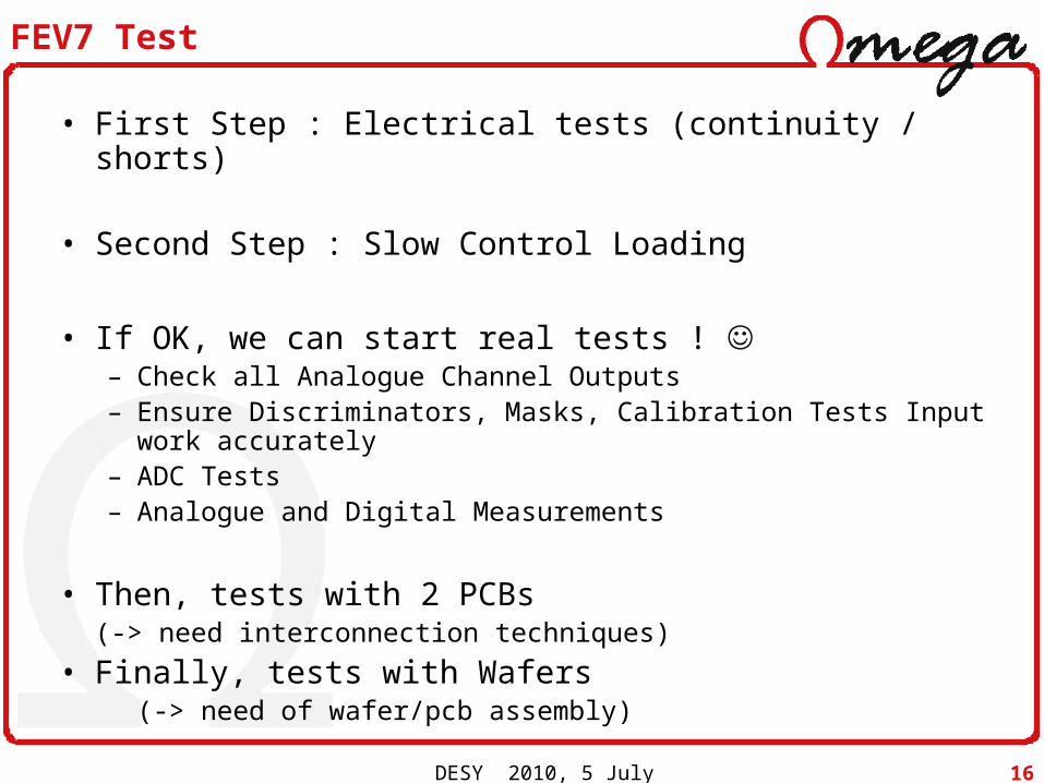
FEV7 Test
• First Step : Electrical tests (continuity / shorts)
• Second Step : Slow Control Loading
• If OK, we can start real tests ! – Check all Analogue Channel Outputs– Ensure Discriminators, Masks, Calibration Tests Input work
accurately– ADC Tests– Analogue and Digital Measurements
• Then, tests with 2 PCBs (-> need interconnection techniques)
• Finally, tests with Wafers(-> need of wafer/pcb assembly)

DESY 2010, 5 July 17
FEV7 COB2: Chip Embedding
Pile-upTop GND cover layerC2 GND + Input chip signalC3 horizontal routing + DVDD + GNDC4 AVDDC5 GND + vertical routingC6 GND (pads signal shielding)C7 pads routingC8 GND (pads shielding)BOT PADS
5 drilling sequences :- Laser C8-C9 120µ filled- Laser C7-C8 120µ- Mechanical C2-C8 200µ- Mechanical C1-C8 200µ- Mechanical C1-C9 (for PCB fastening)
PCB Thickness 1100 µm
DESY 2010, 5 July 18
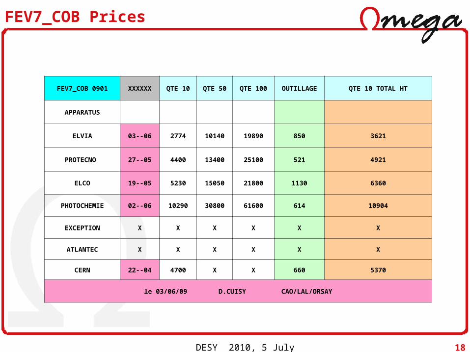
FEV7_COB Prices
FEV7_COB 0901 XXXXXX QTE 10 QTE 50 QTE 100 OUTILLAGE QTE 10 TOTAL HT
APPARATUS
ELVIA 03--06 2774 10140 19890 850 3621
PROTECNO 27--05 4400 13400 25100 521 4921
ELCO 19--05 5230 15050 21800 1130 6360
PHOTOCHEMIE 02--06 10290 30800 61600 614 10904
EXCEPTION X X X X X X
ATLANTEC X X X X X X
CERN 22--04 4700 X X 660 5370
le 03/06/09 D.CUISY CAO/LAL/ORSAY

DESY 2010, 5 July 19
FEV7-COB2 Cost
• FEV7-CIP & FEV7-COB board manufactured by 2 companies to ensure successful result
• FEV7-COB2 prices
• We have lost 1 manufacturer !!
FEV7_COB2 09xx XXXXXX QTE 10 QTE 50 QTE 100 OUTILLAGE QTE 10 TOTAL HT
ELVIA 29--10 3325 12980 26240 900 4225
PROTECNO 23--10 13000 600 13600
le 30/10/09 D.CUISY CAO/LAL/ORSAY

DESY 2010, 5 July 20
Engineering run
• Reticle size : 18x25 mm2– 50-55 reticles/Wafer– 25 wafers needed
• Final arrangement:
– « Calice » chips produced:
• 7 Hardroc 2b => ~9000 chips• 1 Spiroc 2a => ~1200 chips• 1 Spiroc 2b => ~1200 chips• 1 Skiroc 2 => ~1200 chips
– Additionnal chips produced:
• 1 Spaciroc : JEM EUSO experiement• 1 Maroc 3 : for PMT readout• 3 Spiroc 0 (SPIROC « light » version)• => cost reduction for CALICE
• Production run launched last week
SPIROCAnalog HCAL(SiPM)36 ch. 32mm²June 07
HARDROCDigital HCAL(RPC, µmegas or GEMs)64 ch. 16mm²Sept 06
SKIROCECAL(Si PIN diode)36 ch. 20mm²Nov 06
E-CAL
H-CAL
(analog or digital)

DESY 2010, 5 July 21
FEV7-CIP Report
• Plated Through Hole Cross Section :
Blind via (C7-C8) Buried via (C6-C7) Mechanical (C1-C7)
• 2 Manufacturers :– Elvia : 10 PCB received– Protechno : 10 PCB received
• Manufacturers report :– Thickness Measured : 0.90mm to 1.00mm (0.96 desired)– Metal minimum thickness on vias : 25µm