cse237a homework #2 solutions 1. solution. you are given five tasks (t1-5) and five different hw...
TRANSCRIPT
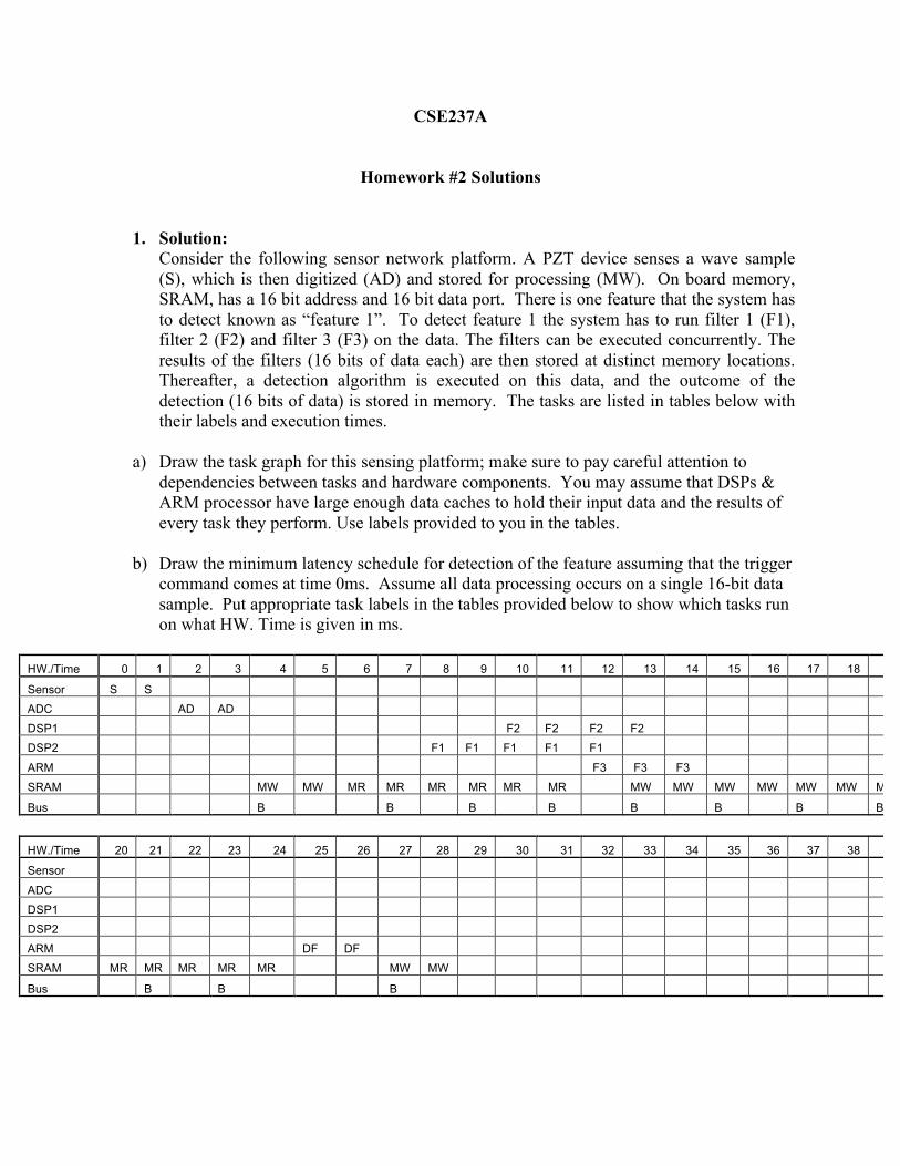
CSE237A
Homework #2 Solutions
1. Solution:
Consider the following sensor network platform. A PZT device senses a wave sample (S), which is then digitized (AD) and stored for processing (MW). On board memory, SRAM, has a 16 bit address and 16 bit data port. There is one feature that the system has to detect known as “feature 1”. To detect feature 1 the system has to run filter 1 (F1), filter 2 (F2) and filter 3 (F3) on the data. The filters can be executed concurrently. The results of the filters (16 bits of data each) are then stored at distinct memory locations. Thereafter, a detection algorithm is executed on this data, and the outcome of the detection (16 bits of data) is stored in memory. The tasks are listed in tables below with their labels and execution times.
a) Draw the task graph for this sensing platform; make sure to pay careful attention to
dependencies between tasks and hardware components. You may assume that DSPs & ARM processor have large enough data caches to hold their input data and the results of every task they perform. Use labels provided to you in the tables.
b) Draw the minimum latency schedule for detection of the feature assuming that the trigger command comes at time 0ms. Assume all data processing occurs on a single 16-bit data sample. Put appropriate task labels in the tables provided below to show which tasks run on what HW. Time is given in ms.
HW./Time 0 1 2 3 4 5 6 7 8 9 10 11 12 13 14 15 16 17 18 19
Sensor S S
ADC AD AD
DSP1 F2 F2 F2 F2
DSP2 F1 F1 F1 F1 F1
ARM F3 F3 F3
SRAM MW MW MR MR MR MR MR MR MW MW MW MW MW MW MR MR
Bus B B B B B B B B
HW./Time 20 21 22 23 24 25 26 27 28 29 30 31 32 33 34 35 36 37 38 39
Sensor
ADC
DSP1
DSP2
ARM DF DF
SRAM MR MR MR MR MR MW MW
Bus B B B
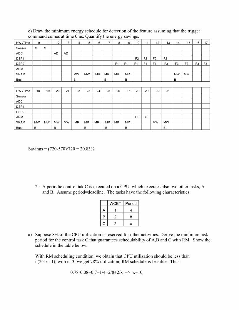
c) Draw the minimum energy schedule for detection of the feature assuming that the trigger command comes at time 0ms. Quantify the energy savings.
HW./Time 0 1 2 3 4 5 6 7 8 9 10 11 12 13 14 15 16 17
Sensor S S
ADC AD AD
DSP1 F2 F2 F2 F2
DSP2 F1 F1 F1 F1 F1 F3 F3 F3 F3 F3
ARM
SRAM MW MW MR MR MR MR MW MW
Bus B B B B
HW./Time 18 19 20 21 22 23 24 25 26 27 28 29 30 31
Sensor
ADC
DSP1
DSP2
ARM DF DF
SRAM MW MW MW MW MR MR MR MR MR MR MW MW
Bus B B B B B B
Savings = (720-570)/720 = 20.83%
2. A periodic control tak C is executed on a CPU, which executes also two other tasks, A and B. Assume period=deadline. The tasks have the following characteristics:
WCET Period
A 1 4
B 2 8
C 2 x a) Suppose 8% of the CPU utilization is reserved for other activities. Derive the minimum task
period for the control task C that guarantees schedulability of A,B and C with RM. Show the schedule in the table below.
With RM scheduling condition, we obtain that CPU utilization should be less than n(2^1/n-1); with n=3, we get 78% utilization; RM schedule is feasible. Thus:
0.78-0.08=0.7=1/4+2/8+2/x => x=10

Therefore, the scheduling priorities are: A, B, C Time 0 1 2 3 4 5 6 7 8 9 10 11 12 13 14 15 16 17 18 19 Task A B B C A C A B B C A C A B B Time 20 21 22 23 24 25 26 27 28 29 30 31 32 33 34 35 36 37 38 39 Time A C C A B B A C C A B B A
b) Due to special design constraints task C has to be executed every 8 time units. Assume that
start times for tasks A,B & C are 2,1 and 0 respectively. From that point on they repeat with period shown in the table (e.g. if task A has the highest priority, it would be scheduled at time 2, 6, 10 etc.). Schedule the tasks with EDF.
Since task C executes every 8 time units, now the schedule will repeat with period 8. Time 0 1 2 3 4 5 6 7 8 9 10 11 12 13 14 15 16 17 18 19
Task C C A B B A C C A B B A C C A B
Time 20 21 22 23 24 25 26 27 28 29 30 31 32 33 34 35 36 37 38 39 Task B A C C A B B A C C A B B A
c) RM: easier to implement, low overhead (O(1)), inefficient EDF: more complex, more resource efficient (higher utilization of computational resources.
3. Consider a system on chip comprising of following components: a CPU, memory, DMA
controller and a network card connected with a system bus. Assume servicing moves data from the peripheral to the memory. The DMA and network card are memory mapped, so they can be directly accessed using instructions that are used for memory accesses as well. Provide a block diagram illustrating what happens during an interrupt generated by the network card for a packet arrival with its description. The interrupt service routine (ISR) for handling the interrupt is installed at memory location (0x100). Also provide the pseudo code for the ISR, which does the following: programs the DMA registers for the transfer of arrived packet (size 4096 bytes) from the network card to memory location 0x200 and clears the interrupt on network card (can be done by writing 0 on the n/w control register). Assume the following:
• DMA has four registers: 1) DMA src reg (0xc100), 2) DMA destination register (0xc200), 3) DMA buf size register (0xc300), 4) DMA ctrl register (0xc400): writing 0x1 initiates the DMA transfer.

• Network card buffer is located at 0xf200 and has a n/w ctrl reg (0xf100), writing 0x0 to which clears the outstanding interrupt.
• The CPU supports two types of instructions: 1) MOV Rx, C: Moves C to register Rx; 2) MEM Rx, M: Moves contents of Rx to memory location M. Describe your timing diagram and the ISR functionality.
Description of what happens: 1(a): µP is executing its main program 1(b): Network card receives packet, which is stored at address 0xf200 2: Network card asserts Int to request servicing by the microprocessor 3: After completing instruction, µP sees Int asserted, saves the PC’s value, and sets PC to the ISR fixed location of 0x100. 4: The ISR reads data from 0x8000, modifies the data, and writes the resulting data to 0x8001. 5: The ISR programs the DMA for transfer of 4096 bytes from 0xf200 to memory location 0x200. 5: The ISR deasserts Int. 6: The ISR returns, thus restoring PC, where µP can resumes executing.
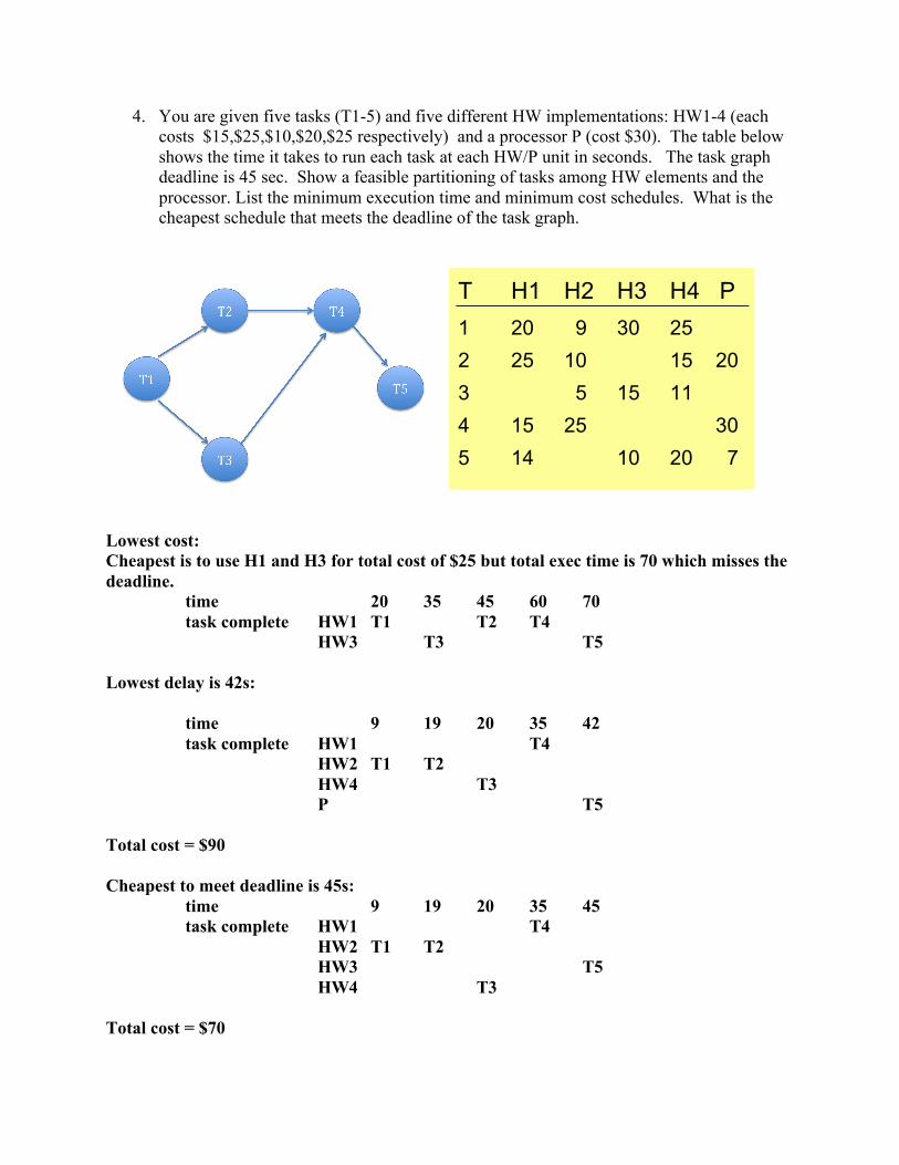
4. You are given five tasks (T1-5) and five different HW implementations: HW1-4 (each costs $15,$25,$10,$20,$25 respectively) and a processor P (cost $30). The table below shows the time it takes to run each task at each HW/P unit in seconds. The task graph deadline is 45 sec. Show a feasible partitioning of tasks among HW elements and the processor. List the minimum execution time and minimum cost schedules. What is the cheapest schedule that meets the deadline of the task graph.
T H1 H2 H3 H4 P
1 20 9 30 25 2 25 10 15 20 3 5 15 11 4 15 25 30 5 14 10 20 7
Lowest cost: Cheapest is to use H1 and H3 for total cost of $25 but total exec time is 70 which misses the deadline.
time 20 35 45 60 70 task complete HW1 T1 T2 T4 HW3 T3 T5
Lowest delay is 42s:
time 9 19 20 35 42 task complete HW1 T4 HW2 T1 T2 HW4 T3 P T5
Total cost = $90 Cheapest to meet deadline is 45s:
time 9 19 20 35 45 task complete HW1 T4 HW2 T1 T2 HW3 T5 HW4 T3
Total cost = $70
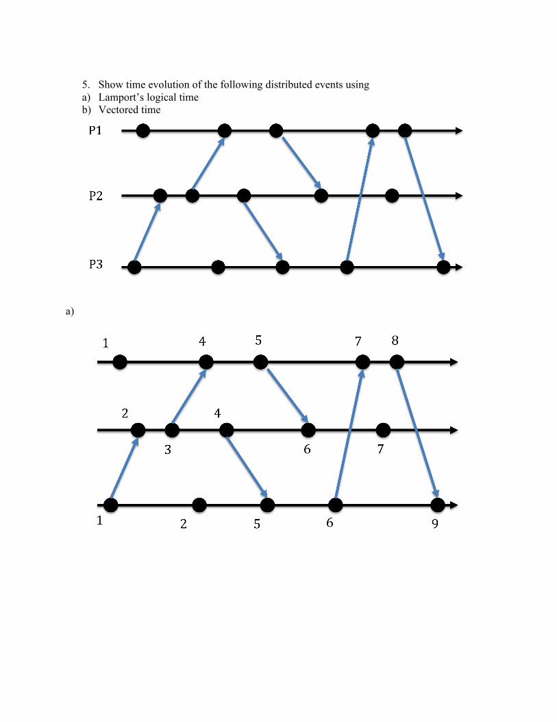
5. Show time evolution of the following distributed events using a) Lamport’s logical time b) Vectored time
a)

b)
