cse140: components and design techniques for … · cse140: components and design techniques for...
TRANSCRIPT

Sources: TSR, Katz, Boriello, Vahid, D & S Harris
CSE140: Components and Design Techniques
for Digital Systems
Adders, multipliers and other ALU elements
Prof. Tajana Simunic Rosing

Sources: TSR, Katz, Boriello, Vahid, D & S Harris
Original grades:
• Max score : 99
• Min score: 13.5
• Mean score : 66
CSE140a Midterm2 Stats
0.0%
5.0%
10.0%
15.0%
Stu
de
nts
(%
)
Points
Midterm2 Original Grade Distribution
buckets # students students (%)
0 ~ 5 11 7.97%
5 ~ 10 0 0.00%
10 ~ 15 1 0.72%
15 ~ 20 1 0.72%
20 ~ 25 3 2.17%
25 ~ 30 2 1.45%
30 ~ 35 5 3.62%
35 ~ 40 10 7.25%
40 ~ 45 6 4.35%
45 ~ 50 6 4.35%
50 ~ 55 7 5.07%
55 ~ 60 7 5.07%
60 ~ 65 9 6.52%
65 ~ 70 10 7.25%
70 ~ 75 11 7.97%
75 ~ 80 10 7.25%
80 ~ 85 7 5.07%
85 ~ 90 13 9.42%
90 ~ 95 13 9.42%
95 ~ 100 6 4.35% Curved grades:
• Max score : 100
• Min score (w/o 0s) : 26
• Mean score : 75

Sources: TSR, Katz, Boriello, Vahid, D & S Harris
Where we are now • What we’ve covered so far:
– Chap 1, 2, 3
– We will skip chap 4 – it is on Verilog which you are learning in 140L
• Logistics:
– HW #7 assigned
– Added HW #8 due Monday 6/10/13 at 8pm via email or in person to
Sheila/TAs/Prof; solutions posted right after 8pm
– The lowest grade of the HWs will be dropped
• CAPEs: http://www.cape.ucsd.edu/
– If participation rate is > 85%, 2nd lowest grade of HWs will be dropped
• Where we are going next:
– Chap 5: components that make a CPU: adders, multipliers, ALU,
counters, registers, memory
– RTL: Chap 5 from Vahid’s textbook is uploaded on the schedule page

Sources: TSR, Katz, Boriello, Vahid, D & S Harris
A B
0 0
0 1
1 0
1 1
0
1
1
0
SCout
0
0
0
1
S = A B
Cout
= AB
Half
Adder
A B
S
Cout +
A B
0 0
0 1
1 0
1 1
0
1
1
0
SCout
0
0
0
1
S = A B Cin
Cout
= AB + ACin
+ BCin
Full
Adder
Cin
0 0
0 1
1 0
1 1
0
0
0
0
1
1
1
1
1
0
0
1
0
1
1
1
A B
S
Cout
Cin+
1-Bit Adders

Sources: TSR, Katz, Boriello, Vahid, D & S Harris
A B
S
Cout
Cin+
N
NN
• Types of carry propagate adders (CPAs):
– Ripple-carry (slow)
– Carry-lookahead (faster)
• Carry-lookahead requires more hardware
Symbol
Multibit Adders (CPAs)

Sources: TSR, Katz, Boriello, Vahid, D & S Harris
S31
A30
B30
S30
A1
B1
S1
A0
B0
S0
C30
C29
C1
C0
Cout ++++
A31
B31
Cin
• Chain 1-bit adders together
• Carry ripples through entire chain
• Disadvantage: slow
Ripple-Carry Adder
tripple = NtFA
where tFA is the delay of a full adder
• Ripple-carry adder delay
A
A
B
B Cin Cout
@0
@0
@0 @0
@N
@1
@1
@N+1
@N+2
late arriving signal
two gate delays to compute Cout

Sources: TSR, Katz, Boriello, Vahid, D & S Harris
Pi @ 1 gate delay
Ci Si @ 2 gate delays
Bi Ai
Gi @ 1 gate delay
G3
C0
C0
C0
C0
P0
P0
P0
P0 G0
G0
G0
G0 C1 @ 3
P1
P1
P1
P1
P1
P1
G1
G1
G1
C2 @ 3
P2
P2
P2
P2
P2
P2
G2
G2
C3 @ 3
P3
P3
P3
P3
C4 @ 3
increasingly complex
logic for carries
Carry-lookahead adders
• Adder with propagate (P) and generate (G) outputs:
• Evaluate Sum and Ci+1
– Sum = Ai xor Bi xor Ci
– Ci+1 = Ai Bi + Ai Ci + Bi Ci
= Ai Bi + Ci (Ai xor Bi)
= Gi + Ci Pi
Sources: TSR, Katz, Boriello, Vahid, D & S Harris
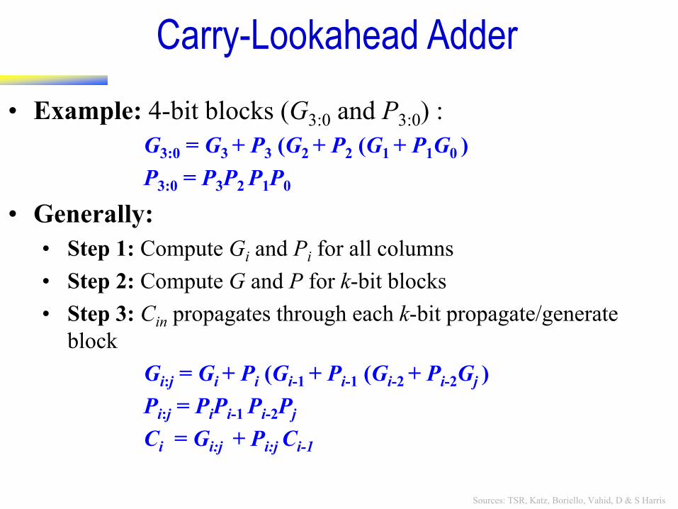
• Example: 4-bit blocks (G3:0 and P3:0) :
G3:0 = G3 + P3 (G2 + P2 (G1 + P1G0 )
P3:0 = P3P2 P1P0
• Generally:
• Step 1: Compute Gi and Pi for all columns
• Step 2: Compute G and P for k-bit blocks
• Step 3: Cin propagates through each k-bit propagate/generate
block
Gi:j = Gi + Pi (Gi-1 + Pi-1 (Gi-2 + Pi-2Gj )
Pi:j = PiPi-1 Pi-2Pj
Ci = Gi:j + Pi:j Ci-1
Carry-Lookahead Adder

Sources: TSR, Katz, Boriello, Vahid, D & S Harris
B0
++++
P3:0
G3
P3
G2
P2
G1
P1
G0
P3
P2
P1
P0
G3:0
Cin
Cout
A0
S0
C0
B1
A1
S1
C1
B2
A2
S2
C2
B3
A3
S3
Cin
A3:0
B3:0
S3:0
4-bit CLA
BlockC
in
A7:4
B7:4
S7:4
4-bit CLA
Block
C3
C7
A27:24
B27:24
S27:24
4-bit CLA
Block
C23
A31:28
B31:28
S31:28
4-bit CLA
Block
C27
Cout
32-bit CLA with 4-bit Blocks

Sources: TSR, Katz, Boriello, Vahid, D & S Harris
For N-bit CLA with k-bit blocks:
tCLA = tpg + tpg_block + (N/k – 1)tAND_OR + ktFA
– tpg : delay to generate all Pi, Gi
– tpg_block : delay to generate all Pi:j, Gi:j
– tAND_OR : delay from Cin to Cout of final AND/OR gate in k-bit CLA
block
An N-bit carry-lookahead adder is generally much faster than a
ripple-carry adder for N > 16
Carry-Lookahead Adder Delay

Sources: TSR, Katz, Boriello, Vahid, D & S Harris
Symbol Implementation
+
A B
-
YY
A B
NN
N
N N
N
N
Subtractor
Logic 1
Sources: TSR, Katz, Boriello, Vahid, D & S Harris
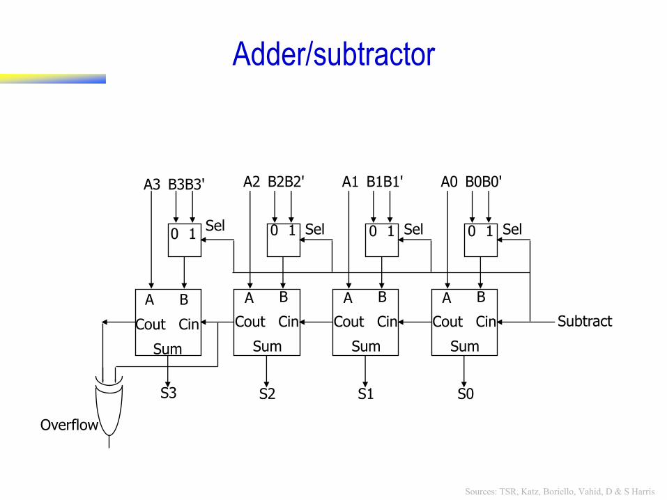
A B
Cout
Sum
Cin
0 1
Subtract
A0 B0 B0'
Sel
Overflow
A B
Cout
Sum
Cin
A1 B1 B1'
Sel
A B
Cout
Sum
Cin
A2 B2 B2'
Sel 0 1 0 1 0 1
A B
Cout
Sum
Cin
A3 B3 B3'
Sel
S3 S2 S1 S0
Adder/subtractor

Sources: TSR, Katz, Boriello, Vahid, D & S Harris
Symbol Implementation
A3
B3
A2
B2
A1
B1
A0
B0
Equal=
A B
Equal
44
Comparator: Equality
Sources: TSR, Katz, Boriello, Vahid, D & S Harris
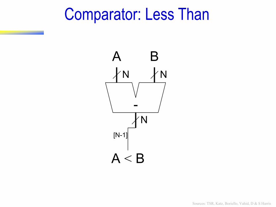
A < B
-
BA
[N-1]
N
N N
Comparator: Less Than

Sources: TSR, Katz, Boriello, Vahid, D & S Harris
ALU
N N
N
3
A B
Y
F
F2:0 Function
000 A & B
001 A | B
010 A + B
011 not used
100 A & ~B
101 A | ~B
110 A - B
111 SLT
Arithmetic Logic Unit (ALU)
+
2 01
A B
Cout
Y
3
01
F2
F1:0
[N-1] S
NN
N
N
N NNN
N
2
Ze
ro
Exte
nd

Sources: TSR, Katz, Boriello, Vahid, D & S Harris
+
2 01
A B
Cout
Y
3
01
F2
F1:0
[N-1] S
NN
N
N
N NNN
N
2
Ze
ro
Exte
nd
• SLT: If A<B then Y=1, else Y=0
• Configure 32-bit ALU for SLT
operation: A = 25 and B = 32
– A < B, so Y should be 32-bit
representation of 1 (0x00000001)
– F2:0 = 111
– F2 = 1 (subtracting), so 25 - 32 = -7
– -7 has 1 in the MSB (S31 = 1)
– F1:0 = 11 multiplexer selects Y = S31
(zero extended) = 0x00000001.
Set Less Than (SLT) Example

Sources: TSR, Katz, Boriello, Vahid, D & S Harris
• Logical shifter: shifts value to left or right and fills empty
spaces with 0’s. Can multiply/divide unsigned #s by 2.
– Ex: 11001 >> 2 = 00110
– Ex: 11001 << 2 = 00100
• Arithmetic shifter: same as logical shifter, but on right shift,
fills empty spaces with the old most significant bit (msb).
Shifting right by n bits on a two's complement signed binary
number has the effect of dividing it by 2n, rounding down.
– Ex: 11001 >>> 2 = 11110
– Ex: 11001 <<< 2 = 00100
• Rotator: rotates bits in a circle, such that bits shifted off one
end are shifted into the other end
– Ex: 11001 ROR 2 = 01110
– Ex: 11001 ROL 2 = 00111
Shifters

Sources: TSR, Katz, Boriello, Vahid, D & S Harris
4 x 4 Multiplier Array
x B3
B2
B1
B0
A3B
0 A
2B
0 A
1B
0 A
0B
0
A3
A2
A1
A0
A3B
1 A
2B
1 A
1B
1 A
0B
1
A3B
2 A
2B
2 A
1B
2 A
0B
2
A3B
3 A
2B
3 A
1B
3 A
0B
3+
P7
P6
P5
P4
P3
P2
P1
P0
0
P2
0
0
0
P1
P0
P5
P4
P3
P7
P6
A3
A2
A1
A0
B0
B1
B2
B3
x
A B
P
44
8

Sources: TSR, Katz, Boriello, Vahid, D & S Harris
CSE140: Components and Design Techniques
for Digital Systems
Registers, Counters and Memory
Tajana Simunic Rosing

Sources: TSR, Katz, Boriello, Vahid, D & S Harris
Basic Register
I3 I2 I1 I0
Q3 Q2 Q1Q0
reg(4)
R R R
D Q D Q D Q D Q
OUT1 OUT2 OUT3 OUT4
CLK
IN1 IN2 IN3 IN4
R
Reset
R
Sources: TSR, Katz, Boriello, Vahid, D & S Harris
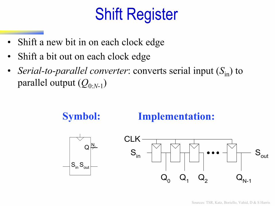
NQ
Sin
Sout
CLK
Sin
Sout
Q0
Q1
QN-1
Q2
Implementation:
• Shift a new bit in on each clock edge
• Shift a bit out on each clock edge
• Serial-to-parallel converter: converts serial input (Sin) to
parallel output (Q0:N-1)
Shift Register
Symbol:

Sources: TSR, Katz, Boriello, Vahid, D & S Harris
Clk0
1
0
1
0
1
0
1
D0
D1
DN-1
D2
Q0
Q1
QN-1
Q2
Sin
Sout
Load
• When Load = 1, acts as a normal N-bit register
• When Load = 0, acts as a shift register
• Now can act as a serial-to-parallel converter (Sin to Q0:N-1) or
a parallel-to-serial converter (D0:N-1 to Sout)
Shift Register with Parallel Load

Sources: TSR, Katz, Boriello, Vahid, D & S Harris
Nth cell
D
Q
CLK
Q[N-1] (left)
Q[N+1] (right)
Input[N]
to N-1th cell
to N+1th cell
clear s0 s1 new value 1 – – 0 0 0 0 output
0 0 1 output value of FF to left (shift right) 0 1 0 output value of FF to right (shift left) 0 1 1 input
Design of a universal shift register
s0 and s1 control mux
0 1 2 3
CLEAR
left_in left_out
right_out
clear right_in
output
input
s0 s1
clock

Sources: TSR, Katz, Boriello, Vahid, D & S Harris
D Q D Q D Q D Q IN
OUT1 OUT2 OUT3 OUT4
CLK
OUT
Pattern recognizer using a shift register

Sources: TSR, Katz, Boriello, Vahid, D & S Harris
Q
CLK
Reset
N
+
N
1
CLK
Reset
N
N
QN
r
Symbol Implementation
• Increments on each clock edge
• Used to cycle through numbers. For example,
– 000, 001, 010, 011, 100, 101, 110, 111, 000, 001…
• Example uses:
– Digital clock displays
– Program counter: keeps track of current instruction executing
Binary Counters

Sources: TSR, Katz, Boriello, Vahid, D & S Harris
EN
D C B A
LOAD
CLR
CLK
RCO
QD QC QB QA
General binary counters
•Default operation: counts up by 1
•QA-QD counter output
•A-D parallel load data
•LOAD enables parallel data load
•RCO ripple carry out – set to 1 if count reaches max value
•CLR clears data
•EN enables the counter

Sources: TSR, Katz, Boriello, Vahid, D & S Harris
Sequence Generator Design
D Q D Q D Q D Q IN
OUT1 OUT2 OUT3 OUT4
CLK
•Sequences through a fixed set of patterns

Sources: TSR, Katz, Boriello, Vahid, D & S Harris
Memory: basic concepts
• Stores large number of bits
– m x n: m words of n bits each
– k = Log2(m) address input signals
– or m = 2^k words
– e.g., 4,096 x 8 memory:
• 32,768 bits
• 12 address input signals
• 8 input/output data signals
• Memory access
– r/w: selects read or write
– enable: read or write only when asserted
– multiport: multiple accesses to different
locations simultaneously
m × n memory
…
…
n bits per word
m w
ord
s
enable
2k × n read and write
memory
A0 …
r/w
…
Q0 Qn-1
Ak-1
memory external view

Sources: TSR, Katz, Boriello, Vahid, D & S Harris
Comparing RAM
• Register file
– Fastest
– But biggest size
• SRAM
– Fast
– More compact than register file
• DRAM
– Slowest
• And refreshing takes time
– But very compact
– Different technology for large caps.
Data
W
Data'
SRAM
Data
W
DRAM
REGISTERS
R R R
D Q D Q D Q D Q
OUT1 OUT2 OUT3 OUT4
CLK
IN1 IN2 IN3 IN4
R

Sources: TSR, Katz, Boriello, Vahid, D & S Harris
RAM Internal Structure
• Similar internal structure as register file
– Decoder enables appropriate word based on address inputs
– rw controls whether cell is written or read
32
10 data
addr
r w
en
1024x32 RAM
addr0 addr1
addr(A-1)
clk
en r w
Let A = log2M
to all cells
wdata(N-1)
rdata(N-1)
wdata(N-2)
rdata(N-2)
wdata0
rdata0
bit storage
block
(aka “cell”)
w o r d
word
RAM cell
word enable
word enable
r w
data cell
data
a0 a1
d0
d1
d(M-1)
a(A-1)
e
AxM
decoder
enable

Sources: TSR, Katz, Boriello, Vahid, D & S Harris
Static RAM (SRAM) - writing
• “Static” RAM cell
– Writing this cell
• word enable input comes from decoder
• When 0, value d loops around inverters
– That loop is where a bit stays stored
• When 1, the data bit value enters the loop
– data is the bit to be stored in this cell
– data’ enters on other side
– Example shows a “1” being written into cell
SRAM cell data data’
d’ d cell
0 word
enable
1
1
1
0
0
32
10 data
addr
r w
en
1024x32 RAM
SRAM cell data data’
d
word
enable
Sources: TSR, Katz, Boriello, Vahid, D & S Harris
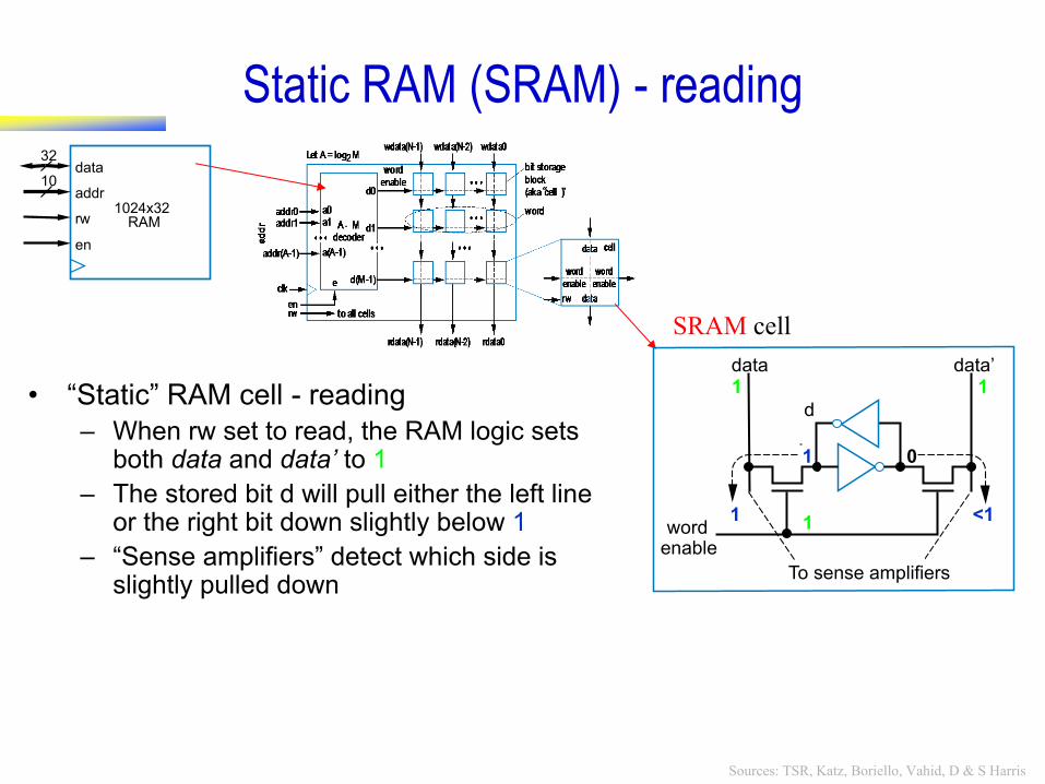
Static RAM (SRAM) - reading
• “Static” RAM cell - reading
– When rw set to read, the RAM logic sets both data and data’ to 1
– The stored bit d will pull either the left line or the right bit down slightly below 1
– “Sense amplifiers” detect which side is slightly pulled down
SRAM cell
32
10 data
addr
r w
en
1024x32 RAM
data data’
d
1
1 1
word enable
To sense amplifiers
1 0
1 <1

Sources: TSR, Katz, Boriello, Vahid, D & S Harris
Dynamic RAM (DRAM)
• “Dynamic” RAM cell
– 1 transistor (rather than 6)
– Relies on large capacitor to store bit
• Write: Transistor conducts, data voltage
level gets stored on top plate of capacitor
• Read: Look at the value of d
• Problem: Capacitor discharges over time
– Must “refresh” regularly, by reading d and
then writing it right back
DRAM cell
32
10 data
addr
r w
en
1024x32 RAM
word
enable
data
c ell
( a )
( b )
data
enable
d discharges
d capacitor
slowly
discharging

Sources: TSR, Katz, Boriello, Vahid, D & S Harris
Read-Only Memory – ROM
• Memory that can only be read from
– Data lines are output only
• Advantages over RAM
– Nonvolatile
– Low power
– Compact
32
10 data
addr
en
1024x32 ROM
ROM block symbol
ROM cell
addr0 addr1
addr(A-1)
clk
en
Let A = log2M
a0 a1
d0
d1
d(M-1)
a(A-1)
e
AxM
decoder
word enable
rdata(N-1) rdata(N-2) rdata0
bit storage
block
(aka “cell”)
w o r d
word enable
word enable
data
data

Sources: TSR, Katz, Boriello, Vahid, D & S Harris
ROM Types
• Erasable Programmable ROM (EPROM)
– Uses “floating-gate transistor” in each cell
– Programmer uses higher-than-normal voltage so electrons tunnel into the gate
• Electrons become trapped in the gate
• Only done for cells that should store 0
• Other cells will be 1
– To erase, shine ultraviolet light onto chip
• Gives trapped electrons energy to escape
• Requires chip package to have window
• Electronically-Erasable Programmable ROM EEPROM
– Programming similar to EPROM
– Erasing one word at a time electronically
• Flash memory
– Like EEPROM, but large blocks can be erased simultaneously
• EEPROM & FLASH are in-system programmable
c ell c ell
word enable
data line data line
e Ð e Ð
trapped electrons
0 1
flo
atin
g-g
ate
tran
sist
or
32
10 data
addr
en
write
busy
1024x32 EEPROM