csci 510/610 lab book - welcome | csusb · pdf filecsci 510/610 lab book keith evan schubert...
TRANSCRIPT
CSCI 510/610 Lab Book
Keith Evan SchubertStudents:
February 3, 2011
Contents
1 Introduction 31.1 Modulo 3 Incrementer . . . . . . . . . . . . . . . . . . . . . . . . 31.2 Test Bench for Modulo 3 Incrementer . . . . . . . . . . . . . . . 51.3 Your Assignment . . . . . . . . . . . . . . . . . . . . . . . . . . . 7
2 Adder With Reservation Stations 82.1 A Simple ALU . . . . . . . . . . . . . . . . . . . . . . . . . . . . 82.2 Test Bench for the Adder . . . . . . . . . . . . . . . . . . . . . . 132.3 Your Assignment . . . . . . . . . . . . . . . . . . . . . . . . . . . 18
3 Register File 193.1 Outline . . . . . . . . . . . . . . . . . . . . . . . . . . . . . . . . 193.2 Test Bench for the Register File . . . . . . . . . . . . . . . . . . . 203.3 Your Assignment . . . . . . . . . . . . . . . . . . . . . . . . . . . 25
4 Instruction Queue 264.1 Outline . . . . . . . . . . . . . . . . . . . . . . . . . . . . . . . . 264.2 Test Bench for the Register File . . . . . . . . . . . . . . . . . . . 284.3 Your Assignment . . . . . . . . . . . . . . . . . . . . . . . . . . . 31
5 Tomasulo’s Method 335.1 Your Assignment . . . . . . . . . . . . . . . . . . . . . . . . . . . 33
6 Calculating the Pentagonal Numbers 346.1 Your Assignment . . . . . . . . . . . . . . . . . . . . . . . . . . . 35
2
Lab 1
Introduction
In this lab manual we will build a simple Tomasulo machine, which will helpyou to understand HDL1 programming in Verilog, as well as how to exploitILP2 using an out of order execution unit. I will assume you have seen someHDL programming before, and given the ease of picking up Verilog any HDLlanguage should be enough. Verilog is one of the coolest languages I know. It isan object oriented, event driven, multi-threaded, intrinsically parallel languagefor simulation and synthesis of logic. There are lots of good language manualsout there so I will concentrate on an example.
1.1 Modulo 3 Incrementer
Listing 1.1: Verilog code of the modulo three incrementer.
module mod3counter (input wire [ 1 : 0 ] num,output reg [ 1 : 0 ] mod3num) ;
always@∗begin
//modulo 3 counter
endendmodule
Consider the code in Listing 1.1. This code declares a single module, whichyou can think of as a class. The module’s name is mod3counter, which is
1Hardware Description Language2Instruction Level Parallelism
3
4 LAB 1. INTRODUCTION
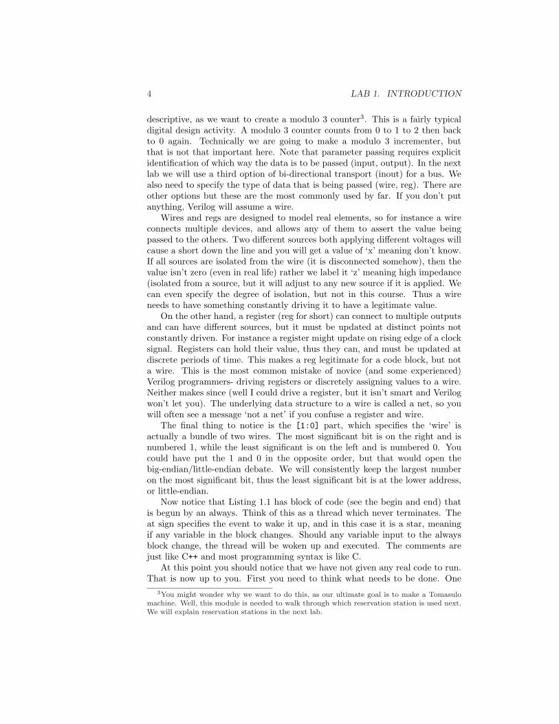
descriptive, as we want to create a modulo 3 counter3. This is a fairly typicaldigital design activity. A modulo 3 counter counts from 0 to 1 to 2 then backto 0 again. Technically we are going to make a modulo 3 incrementer, butthat is not that important here. Note that parameter passing requires explicitidentification of which way the data is to be passed (input, output). In the nextlab we will use a third option of bi-directional transport (inout) for a bus. Wealso need to specify the type of data that is being passed (wire, reg). There areother options but these are the most commonly used by far. If you don’t putanything, Verilog will assume a wire.
Wires and regs are designed to model real elements, so for instance a wireconnects multiple devices, and allows any of them to assert the value beingpassed to the others. Two different sources both applying different voltages willcause a short down the line and you will get a value of ‘x’ meaning don’t know.If all sources are isolated from the wire (it is disconnected somehow), then thevalue isn’t zero (even in real life) rather we label it ‘z’ meaning high impedance(isolated from a source, but it will adjust to any new source if it is applied. Wecan even specify the degree of isolation, but not in this course. Thus a wireneeds to have something constantly driving it to have a legitimate value.
On the other hand, a register (reg for short) can connect to multiple outputsand can have different sources, but it must be updated at distinct points notconstantly driven. For instance a register might update on rising edge of a clocksignal. Registers can hold their value, thus they can, and must be updated atdiscrete periods of time. This makes a reg legitimate for a code block, but nota wire. This is the most common mistake of novice (and some experienced)Verilog programmers- driving registers or discretely assigning values to a wire.Neither makes since (well I could drive a register, but it isn’t smart and Verilogwon’t let you). The underlying data structure to a wire is called a net, so youwill often see a message ‘not a net’ if you confuse a register and wire.
The final thing to notice is the [1:0] part, which specifies the ‘wire’ isactually a bundle of two wires. The most significant bit is on the right and isnumbered 1, while the least significant is on the left and is numbered 0. Youcould have put the 1 and 0 in the opposite order, but that would open thebig-endian/little-endian debate. We will consistently keep the largest numberon the most significant bit, thus the least significant bit is at the lower address,or little-endian.
Now notice that Listing 1.1 has block of code (see the begin and end) thatis begun by an always. Think of this as a thread which never terminates. Theat sign specifies the event to wake it up, and in this case it is a star, meaningif any variable in the block changes. Should any variable input to the alwaysblock change, the thread will be woken up and executed. The comments arejust like C++ and most programming syntax is like C.
At this point you should notice that we have not given any real code to run.That is now up to you. First you need to think what needs to be done. One
3You might wonder why we want to do this, as our ultimate goal is to make a Tomasulomachine. Well, this module is needed to walk through which reservation station is used next.We will explain reservation stations in the next lab.

1.2. TEST BENCH FOR MODULO 3 INCREMENTER 5
way to handle this is write a table of the inputs and outputs, which are quiteshort in this case. Put this in a comment just below the comment in the alwaysblock. Now you need to change the output conditioned on the input, so we willneed a conditional statement. Try searching for both the if-else construct andthe case statement. Which makes the most sense here? Code your choice inthe always block. Notice we can change the output (mod3num) in a code blockbecause it is a reg.
1.2 Test Bench for Modulo 3 Incrementer
Now that we have a module for a modulo 3 incrementer, we need to make aninstance and simulate it for testing purposes. We could later use the sameVerilog code to synthesize logic and program say an FPGA4, but that is thesubject of CSCI 311 and CSCI 521. We only need to simulate and test, sowe need to write a test bench. The terminology goes back to the old days ofhardwired testing (usually with wire wrap), where you would have a physicaltesting bench, which typically was set up to rapidly connect and test circuits.
In any case, our test bench will be another module, but this one will nothave any inputs or outputs, and it will create an instance of our incrementer, seeListing 1.2. Note that there are no parenthesis since there are no parameters.This is a top level module. We will declare two local variables, a reg, to allowus to assign the input, and a wire to receive the output (driven by the reg inthe modulo counter).
Listing 1.2: Verilog code of the modulo 3 counter test bench.
module mod3counter test ;reg [ 1 : 0 ] num in ;wire [ 1 : 0 ] num out ;
mod3counter mod3inc (.num( num in ) ,.mod3num(num out )) ;
i n i t i a lbegin
num in <=2;#10;num in <=1;#10;num in <=0;#10num in <=5;#10;
4Field Programmable Gate Array
6 LAB 1. INTRODUCTION
endendmodule
The instantiation involves declaring first the module name (your new type),followed by an instance name, and the specification of the parameters. Notethat this is not a call to function, it is an instantiation, and the parametersare not values passed per-se, but rather hard connections between entities inthe incrementer and those in the test bench. Don’t get this confused. Youcannot instantiate a module in a thread, such as an always block, as code blocksmanipulate values in hardware, they don’t make hardware. An instantiationmakes hardware. I am declaring a new instance of a piece of hardware, just likea register or wire. Note also how I am passing the values. I am using Verilog-2001 conventions, which are vastly better the the Verilog-1995 conventions usedin many books and online references. Verilog-1995 requires you to place thenames of the external elements you are connecting between the parenthesis in thesame order they are internally. This is basically what most normal programminglanguages do. You might wonder what is so bad about this, particularly giventhat the syntax I am using is much longer (around twice). Well, for smallexamples it is not bad, but for large ones it is easy to get things out of order, orpass the wrong size, which can cause buffer overflow errors (just like in regularprograms). The Verilog-2001 syntax removes the need for the same order bycreating the ‘.internal(external)’ syntax. This allows us to explicitly connectthe entities we want to. Purists might complain the code is not black boxbecause you need to know names from inside the module being instantiated,but you need to know order and such with the other method so it cancels in mymind. The reality is you will get far fewer errors with the Verilog-2001 syntax,so I am requiring it. Note you can switch the order of the two ‘dot’ declarationswithout a problem as long as there is a comma between them.
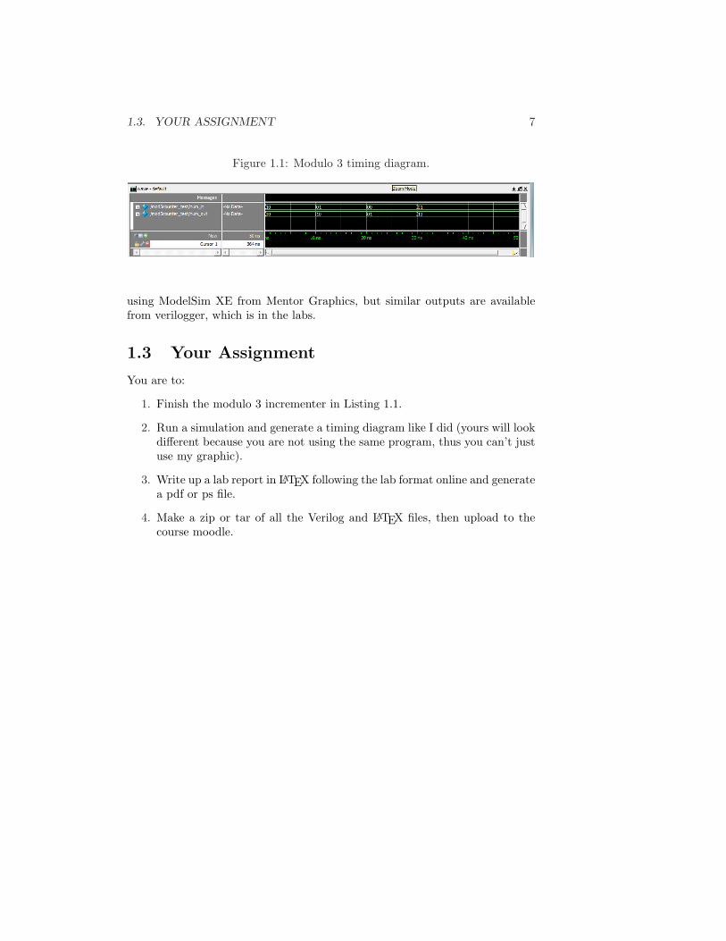
Something new also appears in the main body, an initial block. This isanother thread that starts at the beginning of the simulation (but after instan-tiations), and terminates when the last command is done. Inside the block, wehave non-blocking assignments, <=. There are also blocking assignments likenormal programming languages, =, but you shouldn’t use them unless you havea good reason. Blocking assignments do just what they say, they block thenext statement from happening till they finish, but this doesn’t happen in realphysical elements. One wire doesn’t pass its current, then the next one, it allhappens at once. Multiple non-blocking statements happen in parallel. If wewant to have them happen in order, with some time delay between them, thenwe should be precise in this and put in a time delay, by using the #delay synax.This is just what I do. I set the value of the register then wait 10ns (the defaultsimulation time is 1ns). The final delay is to give time before the simulationends. This is only needed for some simulators, and though mine does not requireit, you might have one that does so I include it for generality. It can’t hurt. Theresulting timing diagram of the simulation is in Figure 1.1. Notice the valuesof the wire bundles are printed in the boxes and the timescale is read on thehorizontal axis. Timing diagrams are immensely useful for debugging. I am
1.3. YOUR ASSIGNMENT 7
Figure 1.1: Modulo 3 timing diagram.
using ModelSim XE from Mentor Graphics, but similar outputs are availablefrom verilogger, which is in the labs.
1.3 Your Assignment
You are to:
1. Finish the modulo 3 incrementer in Listing 1.1.
2. Run a simulation and generate a timing diagram like I did (yours will lookdifferent because you are not using the same program, thus you can’t justuse my graphic).
3. Write up a lab report in LATEX following the lab format online and generatea pdf or ps file.
4. Make a zip or tar of all the Verilog and LATEX files, then upload to thecourse moodle.
Lab 2
Adder With ReservationStations
Now we get to jump in with both feet to the fun stuff. I suggest you read inadvance 2.4-2.6 in the book on Tomasulo’s design for the IBM 360 floating pointunit. You might also find chapter 28 in KOHW helpful.
2.1 A Simple ALU
We want to create a simple ALU, allowing addition, subtraction, and some logicoperations. Typically such devices have no memory, so they just get two valuesand an operation passed in, and the result comes out. We want something alittle more sophisticated. We want to be able to pass in two values and anoperation, but we also want to be able to say if those values are valid values,or the address of something that will produce them, and thus wait for them tobe produced and then calculate. We might have multiple operations before onefinishes, so we want a queue of sorts (we will call these reservation stations) tohold the problems till they can be calculated. Further we might have multipleunits returning results, so we need a bus for transmitting the answers. We willassume the values being calculated are 32 bit, 2’s complement values (specifiedby the signed keyword), and that there might be a total of up to 26 reservationstations total for the computer (thus 6 bit addressing of the reservation stations).We will also assume the system commands are 6 bit, but that only the last 3 bitswill specify the ALU operation (the first 3 bits specify the type of command,and thus the calculation unit). We will use 3 reservation stations for the ALU(in practice I would keep it to powers of 2 if possible, but I am doing this to forceyou to find out how to handle it). This results in a lot of inputs and outputs,see the template in Listing 2.1. Notice the inout declaration, which allows thebi-directional transmission needed for a bus. Some of the features will not beneeded at the moment, they are included for later labs.
8

2.1. A SIMPLE ALU 9
Listing 2.1: Verilog code of the adder.
module adders (input wire c lock , i s sue ,input wire signed [ 3 1 : 0 ] A, B,input wire A inva l id , B inva l id ,input wire [ 5 : 0 ] opcode ,input wire CDB xmit ,inout wire signed [ 3 1 : 0 ] CDB data ,inout wire [ 5 : 0 ] CDB source ,inout wire CDB write ,output reg CDB rts ,output wire ava i l ab l e ,output wire [ 5 : 0 ] RS ava i lab le ,output reg [ 5 : 0 ] i s sued ,output wire [ 5 : 0 ] RS executing ,output reg e r r o r) ;
// cons tan t s
// d i sconnec ted buses have h igh impedianceparameter d i sconnected = 32 ’ bz ;// c a l c u l a t i o n de layparameter delay = 20 ;// updat ing de layparameter update de lay = 5 ;// no un i t i s c a l c u l a t i n gparameter none = 2 ’ b00 ;// c l e a r Qj/Qk , thus Vj/Vk v a l i dparameter va l i d = 6 ’ b000000 ;// error codeparameter no e r r o r = 1 ’ b0 ;parameter a l l r s b u s y = 1 ’ b1 ;// command not i s suedparameter no t i s s u ed = 6 ’ b000000 ;// s t a t u s o f r e s e r v a t i on s t a t i o n or a luparameter not busy = 1 ’ b0 ;parameter i n u s e = 1 ’ b1 ;// i s the va lue ready to send or notparameter ready = 1 ’ b1 ;parameter not ready = 1 ’ b0 ;// used to c l e a r a data va lueparameter c l e a r = 0 ;// r e s e r v a t i on s t a t i o nparameter no r s = 6 ’ b000000 ;
10 LAB 2. ADDER WITH RESERVATION STATIONS
parameter adder 1 = 6 ’ b000001 ;parameter adder 2 = 6 ’ b000010 ;parameter adder 3 = 6 ’ b000011 ;// opera t ion codes used by a luparameter alu add = 3 ’ b000 ;parameter a lu sub = 3 ’ b001 ;parameter a l u o r = 3 ’ b100 ;parameter alu and = 3 ’ b101 ;parameter a lu not = 3 ’ b110 ;parameter a lu xo r = 3 ’ b111 ;
// the r e s u l t be ing wr i t t enreg signed [ 3 1 : 0 ] CDB data out ;// which rs i s f i n i s h e dreg [ 5 : 0 ] CDB source out ;// ready to wr i t e to CDBreg CDB write out ;// opera t ion to doreg [ 5 : 0 ] opera t i on [ 2 : 0 ] ;// i f va l u e s aren ’ t a v a i l a b l e here// i s where to ge t themreg [ 5 : 0 ] Qj [ 2 : 0 ] ,Qk [ 2 : 0 ] ;// va l u e s to c a l c u l a t ereg signed [ 3 1 : 0 ] Vj [ 2 : 0 ] , Vk [ 2 : 0 ] ;// r e s e r v a t i on s t a t i o n f u l l i n d i c a t o r sreg Busy [ 2 : 0 ] ;// a lu c a l c u l a t i n greg Unit Busy ;reg [ 1 : 0 ] a dd e r c a l c u l a t i n g ;// Reservat ion S ta t i on (RS) number o f// each s t a t i o n in t h i s un i treg [ 5 : 0 ] RS num of [ 2 : 0 ] ;// we want to c y c l e the order the// r e s e r v a t i on s t a t i o n s are s e l e c t e d to// go to execu t i on to prevent s t a r v a t i on .reg [ 1 : 0 ] P r i o r i t y S t a t i o n ;wire [ 1 : 0 ] Second Stat ion ;wire [ 1 : 0 ] La s t S ta t i on ;// In termed ia te wires in c a l c u l a t i o n o f a v a i l a b l e RSwire [ 5 : 0 ] RS ava i l a b i l i t y o f S e c ond o r La s t ;wire [ 5 : 0 ] RS a v a i l a b i l i t y o f L a s t ;
// use t r i s t a t e ga t e s to connect the CDB// output r e g i s t e r s to the CDB, wi th// CDB xmit as cont ro l , thus hand l ing wr i t e s
2.1. A SIMPLE ALU 11
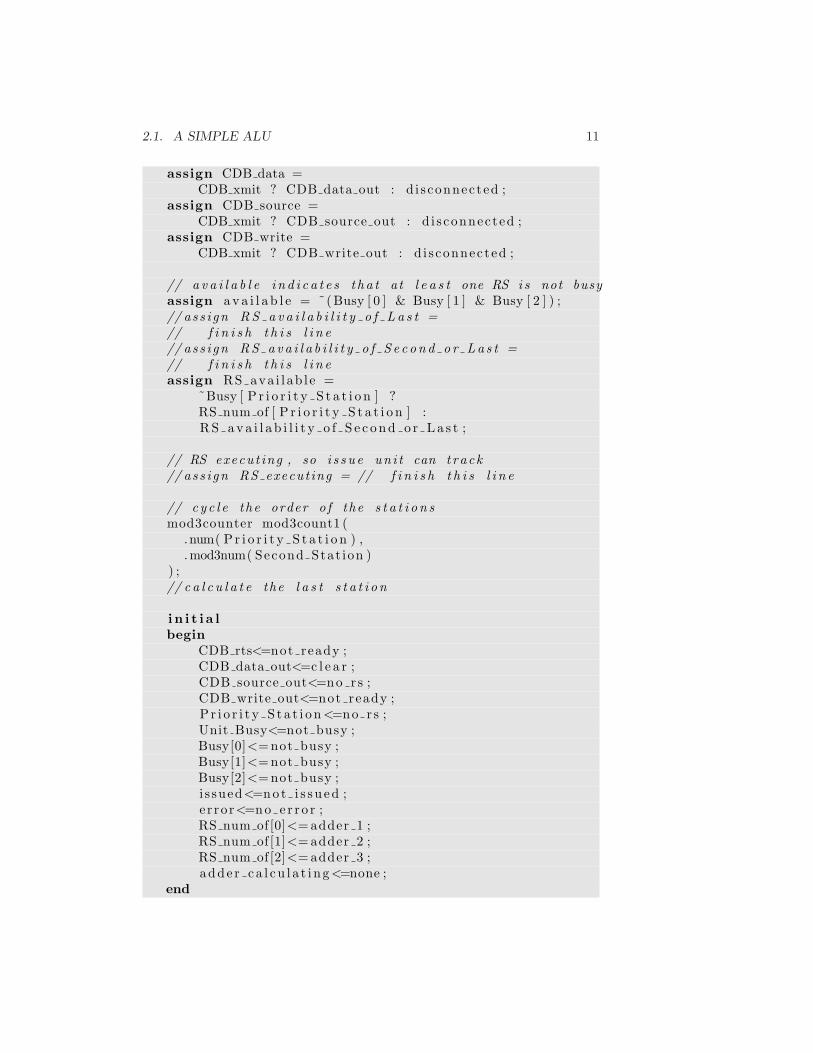
assign CDB data =CDB xmit ? CDB data out : d i s connected ;
assign CDB source =CDB xmit ? CDB source out : d i s connected ;
assign CDB write =CDB xmit ? CDB write out : d i s connected ;
// a v a i l a b l e i n d i c a t e s t ha t a t l e a s t one RS i s not busyassign av a i l a b l e = ˜(Busy [ 0 ] & Busy [ 1 ] & Busy [ 2 ] ) ;// as s i gn RS a v a i l a b i l i t y o f L a s t =// f i n i s h t h i s l i n e// as s i gn RS a v a i l a b i l i t y o f S e c ond o r La s t =// f i n i s h t h i s l i n eassign RS ava i l ab l e =
˜Busy [ P r i o r i t y S t a t i o n ] ?RS num of [ P r i o r i t y S t a t i o n ] :RS ava i l a b i l i t y o f S e c ond o r La s t ;
// RS execut ing , so i s s u e un i t can t rack// as s i gn RS execut ing = // f i n i s h t h i s l i n e
// c y c l e the order o f the s t a t i o n smod3counter mod3count1 (
.num( P r i o r i t y S t a t i o n ) ,
.mod3num( Second Stat ion )) ;// c a l c u l a t e the l a s t s t a t i o n
i n i t i a lbegin
CDB rts<=not ready ;CDB data out<=c l e a r ;CDB source out<=no rs ;CDB write out<=not ready ;P r i o r i t y S t a t i on <=no rs ;Unit Busy<=not busy ;Busy[0]<=not busy ;Busy[1]<=not busy ;Busy[2]<=not busy ;i s sued<=not i s s u ed ;e r ror<=no e r r o r ;RS num of [0]<=adder 1 ;RS num of [1]<=adder 2 ;RS num of [2]<=adder 3 ;adde r ca l cu l a t i ng<=none ;
end

12 LAB 2. ADDER WITH RESERVATION STATIONS
always@ (posedge ( c l o ck ) )begin
// c l ean messages out each c y c l ei s sued<=not i s s u ed ;e r ror<=no e r r o r ;
end
always@ (negedge (CDB xmit ) )begin
// c l ean up wr i t e when f i n i s h e dCDB rts<=not ready ;//CDB write out // f i n i s h t h i s l i n e//Unit Busy // f i n i s h t h i s l i n e//Busy [ a d d e r c a l c u l a t i n g ]// f i n i s h t h i s l i n e// a d d e r c a l c u l a t i n g // f i n i s h t h i s l i n e
end
always@ (posedge ( c l o ck ) )begin
// each c y c l e handle execu t i onend
always@ (negedge ( c l o ck ) )begin
// handle updates
end
always@ (negedge ( c l o ck ) )begin
// handle i s s u eend
endmodule
Let me take a moment to discuss programming style. Note that I am puttingeach type of declaration on a separate line. This is done for readability. Notethat I also try to use names that not only tell you what they are, but that in thecase of boolean values (such as A_invalid) they tell you how to interpret thetrue false values. You should do this, it makes your code vastly more readablewithout introducing ugly comments that only serve to explain your poor namingconventions. In some cases I have used names I don’t like, for instance A or Qj,

2.2. TEST BENCH FOR THE ADDER 13
which are done to remain consistent with naming in the textbook and typicallab manuals for students. To further the aim of making the code readable by ahuman without the need of unnecessary comments, we will declare a bunch ofparameters. These parameters will hold all the values we would normally hardcode in our Verilog. I was contemplating even parameterizing the bit numberingalso, and passing the parameters, but I think that would make it hard to learn.I thus mention for your later reference that we can pass even parameters, thuswe can make a 32 bit processor into a 64 bit processor with a simple parameterchange.
Notice in the parameter section that I use = and not <= as these are donebefore the simulation, so it makes no sense to use non-blocking, which assumesthat time is passing. You should also note that I sometimes write the numbersand other times use statements like 6’b000000. In the number 6’b000000, thepart before the ’ is the number of bits. The b specifies that I am going toenter the number in binary. The 000000 specifies that the value is zero. I couldjust put 0, which will automatically be zero extended, as it is only one bit,but I wanted to be easier to read. You should be careful with sign extension,as sometimes things are zero extended (unsigned numbers and parameters),sometimes they are sign extended (signed numbers), and sometimes you willget an ‘x’ for don’t know. Knowing the sign extension rules greatly simplifiesyour typing and designs.
After the parameters, I declare ‘local variables’, i.e. the internal regs andwires. In a few cases you will see things like reg [5:0] Qj [2:0],Qk [2:0];,which means that Qj and Qk are arrays of arrays, i.e. they have 3 6-bit valueseach. When you address them with only one index you are referring to the 3element array part, not the 6-bit part.
After this I have a few comments, where declarations need to go, then abunch of code blocks. Your job is to fill in these missing portions of the code.I left the code for some of the elements and the initial block to help you outon how I want you to code with the parameters. You should note I have alsointroduced both posedge and negedge, which look for a 0 to 1 transition or 1 to0 transition in the signal that follows respectively. You can only use this in anevent list (i.e. after an @).
Don’t try to guess the code right off the bat, try to think of what needsto happen to accomplish the goal for the block, which I have in the comment.Place an English description of what must happen in you own comments thatfollow my one line comments. Now try to think of how you would code this in C,and it will be very close to Verilog (this was part of the design of the language).Don’t think this will be easy, do your best to think it over before lab, then wewill walk through one of the blocks in lab.
2.2 Test Bench for the Adder
When we have an adder that works, or even before if we wanted to test partsof it, we need to write a test bench to see if it works. Since I have already
14 LAB 2. ADDER WITH RESERVATION STATIONS
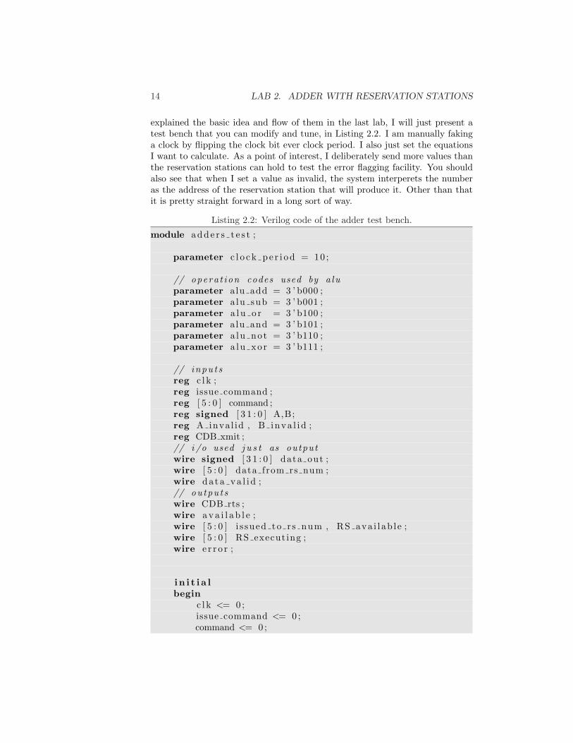
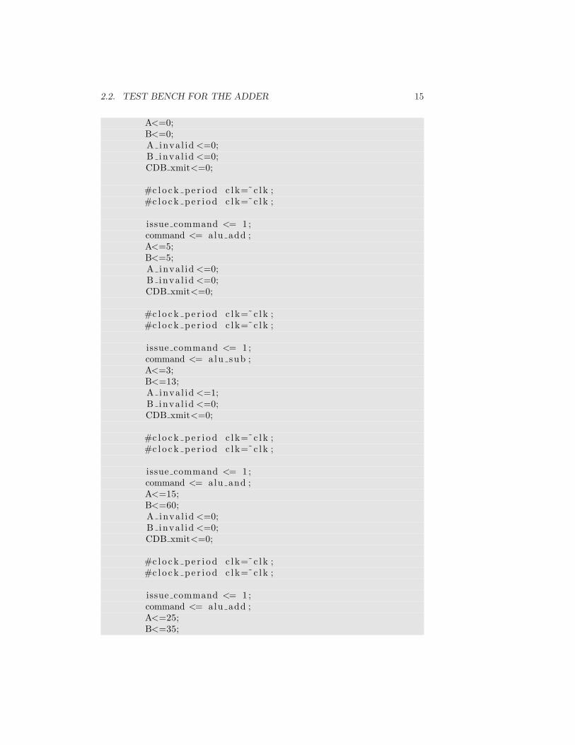
explained the basic idea and flow of them in the last lab, I will just present atest bench that you can modify and tune, in Listing 2.2. I am manually fakinga clock by flipping the clock bit ever clock period. I also just set the equationsI want to calculate. As a point of interest, I deliberately send more values thanthe reservation stations can hold to test the error flagging facility. You shouldalso see that when I set a value as invalid, the system interperets the numberas the address of the reservation station that will produce it. Other than thatit is pretty straight forward in a long sort of way.
Listing 2.2: Verilog code of the adder test bench.
module add e r s t e s t ;
parameter c l o c k p e r i o d = 10 ;
// opera t ion codes used by a luparameter alu add = 3 ’ b000 ;parameter a lu sub = 3 ’ b001 ;parameter a l u o r = 3 ’ b100 ;parameter alu and = 3 ’ b101 ;parameter a lu not = 3 ’ b110 ;parameter a lu xo r = 3 ’ b111 ;
// inpu t sreg c l k ;reg issue command ;reg [ 5 : 0 ] command ;reg signed [ 3 1 : 0 ] A,B;reg A inva l id , B inva l i d ;reg CDB xmit ;// i /o used j u s t as outputwire signed [ 3 1 : 0 ] data out ;wire [ 5 : 0 ] data from rs num ;wire da ta va l i d ;// outpu t swire CDB rts ;wire av a i l a b l e ;wire [ 5 : 0 ] i s sued to r s num , RS ava i l ab l e ;wire [ 5 : 0 ] RS executing ;wire e r r o r ;
i n i t i a lbegin
c l k <= 0 ;issue command <= 0 ;command <= 0 ;
2.2. TEST BENCH FOR THE ADDER 15
A<=0;B<=0;A inva l id <=0;B inva l id <=0;CDB xmit<=0;
#c l o c k p e r i o d c l k=˜c lk ;#c l o c k p e r i o d c l k=˜c lk ;
issue command <= 1 ;command <= alu add ;A<=5;B<=5;A inva l id <=0;B inva l id <=0;CDB xmit<=0;
#c l o c k p e r i o d c l k=˜c lk ;#c l o c k p e r i o d c l k=˜c lk ;
issue command <= 1 ;command <= alu sub ;A<=3;B<=13;A inva l id <=1;B inva l id <=0;CDB xmit<=0;
#c l o c k p e r i o d c l k=˜c lk ;#c l o c k p e r i o d c l k=˜c lk ;
issue command <= 1 ;command <= alu and ;A<=15;B<=60;A inva l id <=0;B inva l id <=0;CDB xmit<=0;
#c l o c k p e r i o d c l k=˜c lk ;#c l o c k p e r i o d c l k=˜c lk ;
issue command <= 1 ;command <= alu add ;A<=25;B<=35;

16 LAB 2. ADDER WITH RESERVATION STATIONS
A inva l id <=0;B inva l id <=0;CDB xmit<=0;
#c l o c k p e r i o d c l k=˜c l k ;#c l o c k p e r i o d c l k=˜c l k ;
issue command <= 0 ;command <= 0 ;A<=0;B<=0;A inva l id <=0;B inva l id <=0;CDB xmit<=0;#c l o c k p e r i o d c l k=˜c l k ;
#c l o c k p e r i o d c l k=˜c l k ;#c l o c k p e r i o d c l k=˜c l k ;
#c l o c k p e r i o d c l k=˜c l k ;#c l o c k p e r i o d c l k=˜c l k ;
#c l o c k p e r i o d c l k=˜c l k ;#c l o c k p e r i o d c l k=˜c l k ;
CDB xmit<=1;
#c l o c k p e r i o d c l k=˜c l k ;#c l o c k p e r i o d c l k=˜c l k ;
CDB xmit<=0;
#c l o c k p e r i o d c l k=˜c l k ;#c l o c k p e r i o d c l k=˜c l k ;
#c l o c k p e r i o d c l k=˜c l k ;#c l o c k p e r i o d c l k=˜c l k ;
#c l o c k p e r i o d c l k=˜c l k ;#c l o c k p e r i o d c l k=˜c l k ;
CDB xmit<=1;
#c l o c k p e r i o d c l k=˜c l k ;#c l o c k p e r i o d c l k=˜c l k ;

2.2. TEST BENCH FOR THE ADDER 17
CDB xmit<=0;
#c l o c k p e r i o d c l k=˜c lk ;#c l o c k p e r i o d c l k=˜c lk ;
#c l o c k p e r i o d c l k=˜c lk ;#c l o c k p e r i o d c l k=˜c lk ;
#c l o c k p e r i o d c l k=˜c lk ;#c l o c k p e r i o d c l k=˜c lk ;
CDB xmit<=1;
#c l o c k p e r i o d c l k=˜c lk ;#c l o c k p e r i o d c l k=˜c lk ;
CDB xmit<=0;
#c l o c k p e r i o d c l k=˜c lk ;#c l o c k p e r i o d c l k=˜c lk ;
end
adders my adders (. c l o ck ( c l k ) ,. i s s u e ( issue command ) ,.A(A) ,.B(B) ,. A inva l id ( A inva l id ) ,. B inva l i d ( B inva l i d ) ,. opcode (command) ,. CDB xmit (CDB xmit ) ,. CDB data ( data out ) ,. CDB source ( data from rs num ) ,. CDB write ( da t a va l i d ) ,. CDB rts (CDB rts ) ,. a v a i l a b l e ( a v a i l a b l e ) ,. RS ava i l ab l e ( RS ava i l ab l e ) ,. i s s u ed ( i s sued to r s num ) ,. RS executing ( RS executing ) ,. e r r o r ( e r r o r )) ;
endmodule
When I run this on my adder and modulo 3 incrementer, I get the timingdiagram in Figure 2.1. Again, yours will look similar, hopefully. The answers

18 LAB 2. ADDER WITH RESERVATION STATIONS
Figure 2.1: Adder timing diagram.
are output only when the CDB_xmit is set to true, i.e. when transmit (xmit)permission is given for the bus. Note the adder holds the values till then.
2.3 Your Assignment
You are to:
1. Finish the adder in Listing 2.1.
2. Run a simulation and generate a timing diagram like I did (yours will lookdifferent because you are not using the same program, thus you can’t justuse my graphic).
3. Write up a lab report in LATEX following the lab format online and generatea pdf or ps file.
4. Make a zip or tar of all the Verilog and LATEX files, then upload to thecourse moodle.
Lab 3
Register File
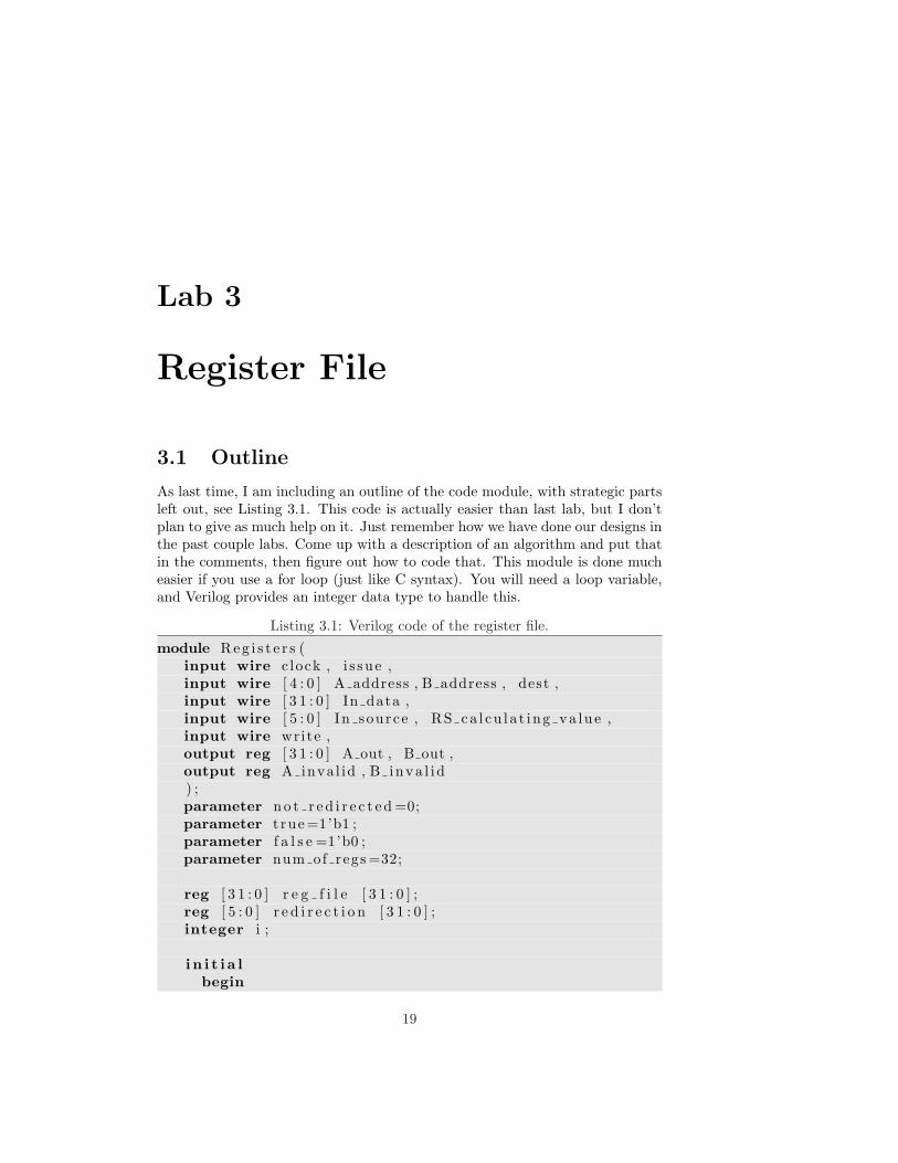
3.1 Outline
As last time, I am including an outline of the code module, with strategic partsleft out, see Listing 3.1. This code is actually easier than last lab, but I don’tplan to give as much help on it. Just remember how we have done our designs inthe past couple labs. Come up with a description of an algorithm and put thatin the comments, then figure out how to code that. This module is done mucheasier if you use a for loop (just like C syntax). You will need a loop variable,and Verilog provides an integer data type to handle this.
Listing 3.1: Verilog code of the register file.
module Reg i s t e r s (input wire c lock , i s sue ,input wire [ 4 : 0 ] A address , B address , dest ,input wire [ 3 1 : 0 ] In data ,input wire [ 5 : 0 ] In source , RS ca l cu l a t ing va lue ,input wire write ,output reg [ 3 1 : 0 ] A out , B out ,output reg A inva l id , B inva l i d) ;parameter no t r e d i r e c t e d =0;parameter t rue =1’b1 ;parameter f a l s e =1’b0 ;parameter num of regs =32;
reg [ 3 1 : 0 ] r e g f i l e [ 3 1 : 0 ] ;reg [ 5 : 0 ] r e d i r e c t i o n [ 3 1 : 0 ] ;integer i ;
i n i t i a lbegin
19

20 LAB 3. REGISTER FILE
for ( i =0; i<num of regs ; i=i +1)begin
r e g f i l e [ i ]= i ;r e d i r e c t i o n [ i ]= no t r e d i r e c t e d ;
endend
always@ (negedge c l o ck )begin
// handle i s s u e send
always@ (posedge c l o ck )begin
// handle updatesend
endmodule
3.2 Test Bench for the Register File
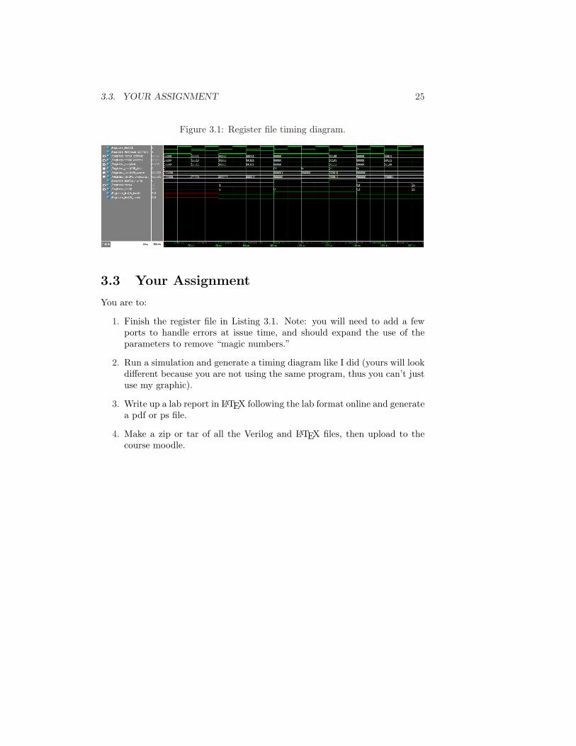
By now you are hopefully comfortable with the concept of designing a testbench. There is nothing surprising in this one at all, see Listing 3.2. The timingdiagram I get is also straightforward, see Figure 3.1.
Listing 3.2: Verilog code of the register file test bench.
module Re g i s t e r s t e s t ;
parameter c l o c k p e r i o d = 10 ;
// inpu t sreg c l k ;reg issue command ;reg [ 4 : 0 ] A address , B address , des t ;reg signed [ 3 1 : 0 ] CDB data ;reg [ 5 : 0 ] CDB source , RS produc ing re su l t ;reg CDB write ;
wire signed [ 3 1 : 0 ] A,B;wire A inva l id , B inva l i d ;
i n i t i a lbegin
3.2. TEST BENCH FOR THE REGISTER FILE 21
c l k <= 0 ;
// read ing v a r i a b l e sissue command <= 0 ;A address <=0;B address <=0;dest <=0;RS produc ing resu l t <=0;
// update v a r i a b l e sCDB data<=0;CDB source<=0;CDB write<=0;
#c l o c k p e r i o d c l k=˜c lk ;#c l o c k p e r i o d c l k=˜c lk ;
// read ing v a r i a b l e sissue command <= 1 ;A address <=1;B address <=2;dest <=3;RS produc ing resu l t <=1;
// update v a r i a b l e sCDB data<=0;CDB source<=0;CDB write<=0;
#c l o c k p e r i o d c l k=˜c lk ;#c l o c k p e r i o d c l k=˜c lk ;
// read ing v a r i a b l e sissue command <= 0 ;A address <=0;B address <=0;dest <=0;RS produc ing resu l t <=0;
// update v a r i a b l e sCDB data<=0;CDB source<=0;
22 LAB 3. REGISTER FILE
CDB write<=0;
#c l o c k p e r i o d c l k=˜c l k ;#c l o c k p e r i o d c l k=˜c l k ;
// read ing v a r i a b l e sissue command <= 1 ;A address <=3;B address <=7;dest <=7;RS produc ing resu l t <=2;
// update v a r i a b l e sCDB data<=0;CDB source<=0;CDB write<=0;
#c l o c k p e r i o d c l k=˜c l k ;#c l o c k p e r i o d c l k=˜c l k ;
// read ing v a r i a b l e sissue command <= 0 ;A address <=0;B address <=0;dest <=0;RS produc ing resu l t <=0;
// update v a r i a b l e sCDB data<=25;CDB source<=1;CDB write<=1;
#c l o c k p e r i o d c l k=˜c l k ;#c l o c k p e r i o d c l k=˜c l k ;
// read ing v a r i a b l e sissue command <= 0 ;A address <=0;B address <=0;

3.2. TEST BENCH FOR THE REGISTER FILE 23
dest <=0;RS produc ing resu l t <=0;
// update v a r i a b l e sCDB data<=0;CDB source<=0;CDB write<=0;
#c l o c k p e r i o d c l k=˜c lk ;#c l o c k p e r i o d c l k=˜c lk ;
// read ing v a r i a b l e sissue command <= 1 ;A address <=12;B address <=13;dest <=15;RS produc ing resu l t <=3;
// update v a r i a b l e sCDB data<=21;CDB source<=2;CDB write<=1;
#c l o c k p e r i o d c l k=˜c lk ;#c l o c k p e r i o d c l k=˜c lk ;
// read ing v a r i a b l e sissue command <= 0 ;A address <=0;B address <=0;dest <=0;RS produc ing resu l t <=0;
// update v a r i a b l e sCDB data<=0;CDB source<=0;CDB write<=0;
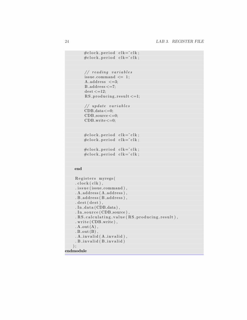
24 LAB 3. REGISTER FILE
#c l o ck p e r i o d c l k=˜c l k ;#c l o c k p e r i o d c l k=˜c l k ;
// read ing v a r i a b l e sissue command <= 1 ;A address <=3;B address <=7;dest <=12;RS produc ing resu l t <=1;
// update v a r i a b l e sCDB data<=0;CDB source<=0;CDB write<=0;
#c l o c k p e r i o d c l k=˜c l k ;#c l o c k p e r i o d c l k=˜c l k ;
#c l o c k p e r i o d c l k=˜c l k ;#c l o c k p e r i o d c l k=˜c l k ;
end
Reg i s t e r s myregs (. c l o ck ( c l k ) ,. i s s u e ( issue command ) ,. A address ( A address ) ,. B address ( B address ) ,. des t ( des t ) ,. In data (CDB data ) ,. I n s ou r c e ( CDB source ) ,. RS ca l cu l a t i ng va lu e ( RS produc ing re su l t ) ,. wr i t e ( CDB write ) ,. A out (A) ,. B out (B) ,. A inva l id ( A inva l id ) ,. B inva l i d ( B inva l i d )
) ;endmodule
3.3. YOUR ASSIGNMENT 25
Figure 3.1: Register file timing diagram.
3.3 Your Assignment
You are to:
1. Finish the register file in Listing 3.1. Note: you will need to add a fewports to handle errors at issue time, and should expand the use of theparameters to remove “magic numbers.”
2. Run a simulation and generate a timing diagram like I did (yours will lookdifferent because you are not using the same program, thus you can’t justuse my graphic).
3. Write up a lab report in LATEX following the lab format online and generatea pdf or ps file.
4. Make a zip or tar of all the Verilog and LATEX files, then upload to thecourse moodle.

Lab 4
Instruction Queue
4.1 Outline
By now, I hope you are comfortable with the idea of developing the algorithmsfor a piece of hardware. The instruction queue needs to handle fetching instruc-tions from memory, issuing instructions when a reservation station is available,tracking the status of an instruction, and removing the instruction from thequeue when it is finished. Memory can be modeled as an array of 32 bit valuesfor simplicity. I suggest you have a program counter that walks through thememory each cycle and fetches to the next available spot in the queue if thereis one. My sample interface is in Listing 4.1.
Listing 4.1: Verilog code of the instruction queue.
module i n s t r u c t i on queue (input wire c lock ,input wire i s s u e e r r o r ,input wire adde r ava i l ab l e ,input wire [ 5 : 0 ] adder RS ava i lab le ,input wire [ 5 : 0 ] RS issued ,input wire [ 5 : 0 ] RS execut ing adder ,input wire adder r t s ,input wire [ 5 : 0 ] RS f in i shed ,output reg [ 5 : 0 ] operat ion ,output reg [ 2 : 0 ] execut i on un i t ,output reg [ 4 : 0 ] Dest address ,output reg [ 4 : 0 ] A address ,output reg [ 4 : 0 ] B address ,output reg i s s u e) ;
parameter TRUE =1’b1 ;parameter FALSE =1’b0 ;
26

4.1. OUTLINE 27
parameter LAST INSTRUCTION ELEMENT = 1023 ;parameter INSTRUCTION ADDRESS BITS = 10 ;parameter LAST QUEUE ELEMENT = 7 ;parameter QUEUE ADDRESS BITS = 3 ;parameter CLEAR =0;parameter OPCODE HIGH = 31 ;parameter OPCODELOW = 26 ;parameter EXEC UNIT HIGH = 31 ;parameter EXEC UNIT LOW = 29 ;parameter SOURCE1 HIGH = 25 ;parameter SOURCE1 LOW = 21 ;parameter SOURCE2 HIGH = 20 ;parameter SOURCE2 LOW = 16 ;parameter DESTINATION HIGH = 15 ;parameter DESTINATION LOW = 11 ;parameter BUSY MASK = 4 ’ b0001 ;parameter ISSUE MASK = 4 ’ b0010 ;parameter EXECUTE MASK = 4 ’ b0100 ;parameter WRITE BACK MASK = 4 ’ b1000 ;parameter ADDER= 3 ’ b000 ;parameter alu add = 3 ’ b000 ;parameter a lu sub = 3 ’ b001 ;parameter a l u o r = 3 ’ b100 ;parameter alu and = 3 ’ b101 ;parameter a lu not = 3 ’ b110 ;parameter a lu xo r = 3 ’ b111 ;
integer i , j ;
reg i s s u e d t h i s c l o c k = 0 ;reg [ 3 1 : 0 ] Instruct ion Memory [LAST INSTRUCTION ELEMENT : 0 ] ;reg [ INSTRUCTION ADDRESS BITS : 0 ] PC=0;reg nex t queue l o ca t i on ;reg [ 3 1 : 0 ] I n s t r u c t i o n [LAST QUEUE ELEMENT: 0 ] ;reg [ 5 : 0 ] RS Holding [LAST QUEUE ELEMENT: 0 ] ;reg [ 3 : 0 ] Status [LAST QUEUE ELEMENT: 0 ] ;reg [QUEUE ADDRESS BITS−1:0 ] Queue End = CLEAR;
i n i t i a lbegin
i s sue<=FALSE;for ( i =0; i<=LAST QUEUE ELEMENT; i=i +1)begin
I n s t r u c t i o n [ i ] <= CLEAR;RS Holding [ i ] <= CLEAR;

28 LAB 4. INSTRUCTION QUEUE
Status [ i ] <= CLEAR;endfor ( i =0; i <=32; i=i +1)begin
Instruct ion Memory [ i ] <= {ADDER , alu add , 5 ’ b00001 ,5 ’ b00011 , 5 ’ b00111 , 11 ’ b0 } ;
endend
endmodule
4.2 Test Bench for the Register File
By now you are hopefully comfortable with the concept of designing a testbench. There is nothing surprising in this one either, see Listing 4.2. Thetiming diagram I get is also straightforward, see Figure 4.1.
Listing 4.2: Verilog code of the instruction queue test bench.
module I n s t r u c t i o n qu eu e t e s t ;
reg c l k =0;reg e r r o r =0;reg av a i l a b l e =0;reg [ 5 : 0 ] RS ava i l ab l e =0;reg [ 5 : 0 ] RS is sue ;reg [ 5 : 0 ] RS exec=0;reg adde r r t s =0;reg [ 5 : 0 ] RS xmit=0;
wire [ 5 : 0 ] opcode ;wire [ 2 : 0 ] e x e c un i t ;wire [ 4 : 0 ] A address ;wire [ 4 : 0 ] B address ;wire [ 4 : 0 ] Dest addres s ;wire i s s u e ;
parameter c l k p e r i o d =10;
i n i t i a l
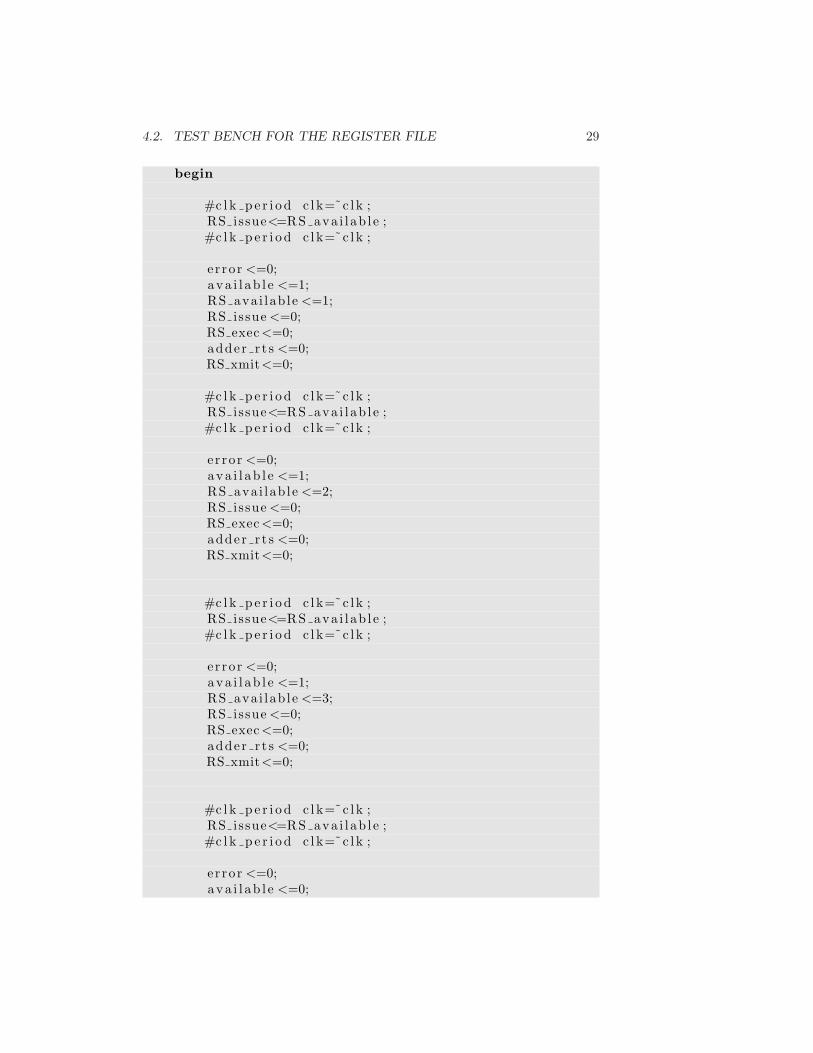
4.2. TEST BENCH FOR THE REGISTER FILE 29
begin
#c l k p e r i o d c l k=˜c lk ;RS issue<=RS ava i l ab l e ;#c l k p e r i o d c l k=˜c lk ;
e r ro r <=0;ava i l ab l e <=1;RS ava i lab le <=1;RS issue <=0;RS exec<=0;adder r t s <=0;RS xmit<=0;
#c l k p e r i o d c l k=˜c lk ;RS issue<=RS ava i l ab l e ;#c l k p e r i o d c l k=˜c lk ;
e r ro r <=0;ava i l ab l e <=1;RS ava i lab le <=2;RS issue <=0;RS exec<=0;adder r t s <=0;RS xmit<=0;
#c l k p e r i o d c l k=˜c lk ;RS issue<=RS ava i l ab l e ;#c l k p e r i o d c l k=˜c lk ;
e r ro r <=0;ava i l ab l e <=1;RS ava i lab le <=3;RS issue <=0;RS exec<=0;adder r t s <=0;RS xmit<=0;
#c l k p e r i o d c l k=˜c lk ;RS issue<=RS ava i l ab l e ;#c l k p e r i o d c l k=˜c lk ;
e r ro r <=0;ava i l ab l e <=0;
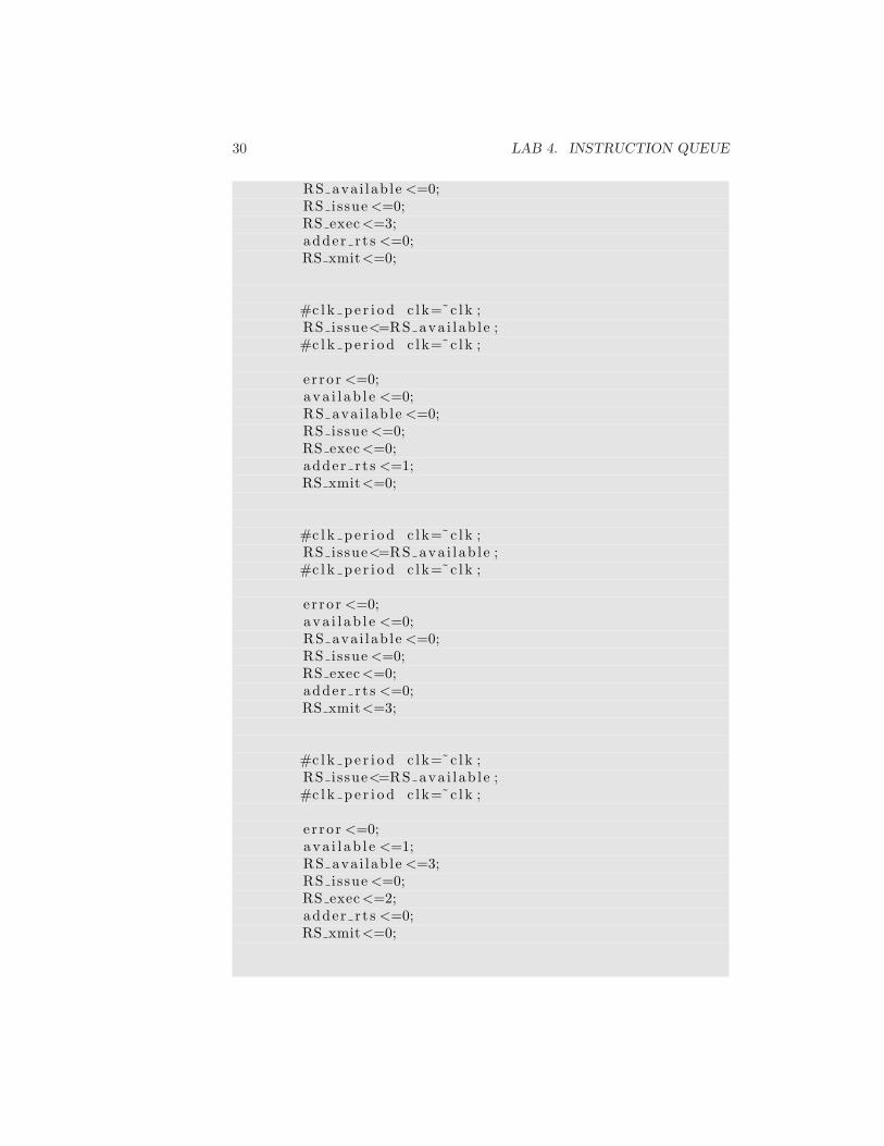
30 LAB 4. INSTRUCTION QUEUE
RS avai lab le <=0;RS issue <=0;RS exec <=3;adder r t s <=0;RS xmit<=0;
#c l k p e r i o d c l k=˜c l k ;RS issue<=RS ava i l ab l e ;#c l k p e r i o d c l k=˜c l k ;
e r ro r <=0;ava i l ab l e <=0;RS ava i lab le <=0;RS issue <=0;RS exec <=0;adder r t s <=1;RS xmit<=0;
#c l k p e r i o d c l k=˜c l k ;RS issue<=RS ava i l ab l e ;#c l k p e r i o d c l k=˜c l k ;
e r ro r <=0;ava i l ab l e <=0;RS ava i lab le <=0;RS issue <=0;RS exec <=0;adder r t s <=0;RS xmit<=3;
#c l k p e r i o d c l k=˜c l k ;RS issue<=RS ava i l ab l e ;#c l k p e r i o d c l k=˜c l k ;
e r ro r <=0;ava i l ab l e <=1;RS ava i lab le <=3;RS issue <=0;RS exec <=2;adder r t s <=0;RS xmit<=0;
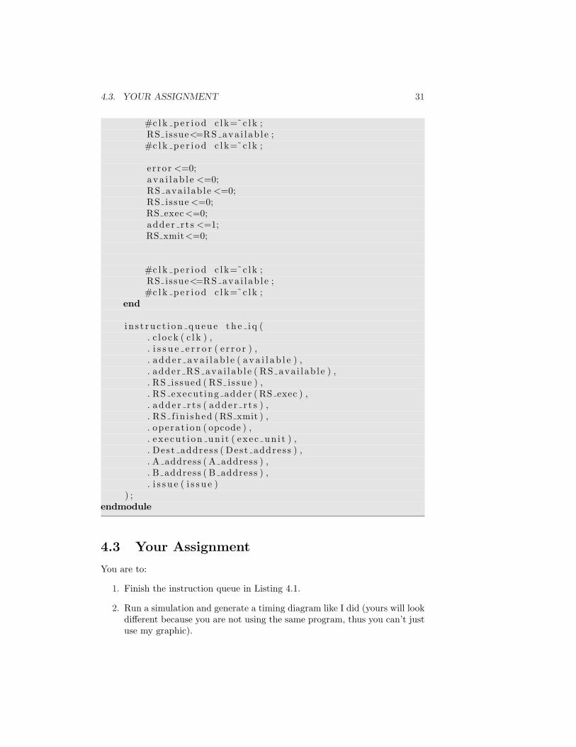
4.3. YOUR ASSIGNMENT 31
#c l k p e r i o d c l k=˜c lk ;RS issue<=RS ava i l ab l e ;#c l k p e r i o d c l k=˜c lk ;
e r ro r <=0;ava i l ab l e <=0;RS ava i lab le <=0;RS issue <=0;RS exec<=0;adder r t s <=1;RS xmit<=0;
#c l k p e r i o d c l k=˜c lk ;RS issue<=RS ava i l ab l e ;#c l k p e r i o d c l k=˜c lk ;
end
i n s t r u c t i on queue t h e i q (. c l o ck ( c l k ) ,. i s s u e e r r o r ( e r r o r ) ,. a dd e r ava i l ab l e ( a v a i l a b l e ) ,. adder RS ava i l ab l e ( RS ava i l ab l e ) ,. RS issued ( RS issue ) ,. RS execut ing adder ( RS exec ) ,. adde r r t s ( adde r r t s ) ,. RS f in i shed ( RS xmit ) ,. opera t i on ( opcode ) ,. e x e cu t i on un i t ( ex e c un i t ) ,. Dest addres s ( Dest addres s ) ,. A address ( A address ) ,. B address ( B address ) ,. i s s u e ( i s s u e )
) ;endmodule
4.3 Your Assignment
You are to:
1. Finish the instruction queue in Listing 4.1.
2. Run a simulation and generate a timing diagram like I did (yours will lookdifferent because you are not using the same program, thus you can’t justuse my graphic).

32 LAB 4. INSTRUCTION QUEUE
Figure 4.1: Instruction Queue timing diagram.
3. Write up a lab report in LATEX following the lab format online and generatea pdf or ps file.
4. Make a zip or tar of all the Verilog and LATEX files, then upload to thecourse moodle.

Lab 5
Tomasulo’s Method
Now it is up to you to combine the previous modules in a main module to makea functioning Tomasulo’s machine.
5.1 Your Assignment
You are to:
1. Write your own module to interface the previously developed ones.
2. Run a simulation and generate a timing diagram. This time there is notestbench, you should only have to set up instruction memory.
3. Write up a lab report in LATEX following the lab format online and generatea pdf or ps file.
4. Make a zip or tar of all the Verilog and LATEX files, then upload to thecourse moodle.
33

Lab 6
Calculating the PentagonalNumbers
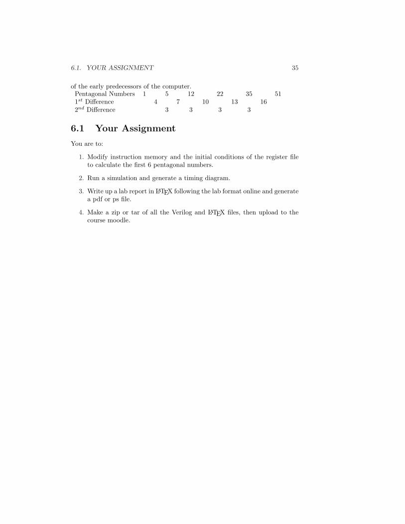
The pentagonal numbers are a mathematical sequence that is an example offigurative numbers. Figurative numbers are the number of dots on an appropri-ately nested sequence of polygons. In the case of the pentagonal numbers, thepolygons are pentagons that share a vertex.
The first several pentagonal numbers are thus {1, 5, 12, 22, 35, 51, 70, 92, . . .}.The challenge is then how do we calculate any pentagonal number using onlyaddition? Sounds daunting, but this is where we stand on the shoulders ofgiants. Isaac Newton came up with a method of differences, which is easilyunderstood from calculus. Assume we have a sequence of numbers, which isdescribed by a polynomial. If we kept taking derivatives you would eventuallyend up with a zero as the answer, which means the previous derivative wasa constant, say k0. That means the derivative before it is just a sum of theconstants k0, with some initial value, say k1. We can then use those numbers toadd to calculate the next level up, and so on, till we eventually reach the actualpolynomial. Interestingly this only involves addition. This cool property wasnoted by Charles Babage, who used it as the basis of the difference engine, one
Figure 6.1: First six pentagonal numbers. Based off a graphic from the CreativeCommons licensed for any use by Timren.
34
6.1. YOUR ASSIGNMENT 35
of the early predecessors of the computer.Pentagonal Numbers 1 5 12 22 35 511st Difference 4 7 10 13 162nd Difference 3 3 3 3
6.1 Your Assignment
You are to:
1. Modify instruction memory and the initial conditions of the register fileto calculate the first 6 pentagonal numbers.
2. Run a simulation and generate a timing diagram.
3. Write up a lab report in LATEX following the lab format online and generatea pdf or ps file.
4. Make a zip or tar of all the Verilog and LATEX files, then upload to thecourse moodle.