cs61c l25 cpu design : designing a single-cycle cpu (1) garcia, fall 2006 © ucb t-mobile’s wi-fi...
Post on 21-Dec-2015
213 views
TRANSCRIPT

CS61C L25 CPU Design : Designing a Single-Cycle CPU (1) Garcia, Fall 2006 © UCB
T-Mobile’s Wi-Fi / Cell phone T-mobile just announced a new
phone that can operate normally as a cell phone, but when it’s near a “T-mobile wireless hotspot” (you could own at home), it switches
to Wi-Fi & calls are FREE. Yes, FREE.
Lecturer SOE Dan Garcia
www.cs.berkeley.edu/~ddgarcia
inst.eecs.berkeley.edu/~cs61c UC Berkeley CS61C : Machine Structures
Lecture 25 – CPU Design: Designing a Single-cycle CPU
2006-10-27
theonlyphoneyouneed.com
QuickTime™ and aTIFF (Uncompressed) decompressor
are needed to see this picture.

CS61C L25 CPU Design : Designing a Single-Cycle CPU (2) Garcia, Fall 2006 © UCB
Five Components of a Computer
Processor
Computer
Control
Datapath
Memory(passive)
(where programs, data live whenrunning)
Devices
Input
Output
Keyboard, Mouse
Display, Printer
Disk (where programs, data live when not running)

CS61C L25 CPU Design : Designing a Single-Cycle CPU (3) Garcia, Fall 2006 © UCB
Datapath Summary• The datapath based on data transfers required to perform instructions
• A controller causes the right transfers to happen
PC
inst
ruct
ion
me
mor
y
+4
rtrs
rd
regi
ste
rs
ALU
Da
tam
em
ory
imm
Controller
opcode, funct

CS61C L25 CPU Design : Designing a Single-Cycle CPU (4) Garcia, Fall 2006 © UCB
CPU clocking
• Single Cycle CPU: All stages of an instruction are completed within one long clock cycle.
• The clock cycle is made sufficient long to allow each instruction to complete all stages without interruption and within one cycle.
For each instruction, how do we control the flow of information though the datapath?
1. InstructionFetch
2. Decode/ Register
Read
3. Execute 4. Memory5. Reg. Write
CS61C L25 CPU Design : Designing a Single-Cycle CPU (5) Garcia, Fall 2006 © UCB
Outline of Today’s Lecture
• Design a processor: step-by-step• Requirements of the Instruction Set
• Hardware components that match the instruction set requirements
• Partial Datapath in detail

CS61C L25 CPU Design : Designing a Single-Cycle CPU (6) Garcia, Fall 2006 © UCB
How to Design a Processor: step-by-step1. Analyze instruction set architecture (ISA)
datapath requirements• meaning of each instruction is given by the register transfers
• datapath must include storage element for ISA registers
• datapath must support each register transfer
2. Select set of datapath components and establish clocking methodology
3. Assemble datapath meeting requirements4. Analyze implementation of each instruction to determine setting of control points that effects the register transfer.
5. Assemble the control logic

CS61C L25 CPU Design : Designing a Single-Cycle CPU (7) Garcia, Fall 2006 © UCB
Review: The MIPS Instruction Formats• All MIPS instructions are 32 bits long. 3 formats:
• R-type
• I-type
• J-type
• The different fields are:• op: operation (“opcode”) of the instruction• rs, rt, rd: the source and destination register specifiers• shamt: shift amount• funct: selects the variant of the operation in the “op”
field• address / immediate: address offset or immediate value• target address: target address of jump instruction
op target address
02631
6 bits 26 bits
op rs rt rd shamt funct
061116212631
6 bits 6 bits5 bits5 bits5 bits5 bits
op rs rt address/immediate
016212631
6 bits 16 bits5 bits5 bits

CS61C L25 CPU Design : Designing a Single-Cycle CPU (8) Garcia, Fall 2006 © UCB
Step 1a: The MIPS-lite Subset for today
• ADDU and SUBU•addu rd,rs,rt•subu rd,rs,rt
• OR Immediate:•ori rt,rs,imm16
• LOAD and STORE Word•lw rt,rs,imm16•sw rt,rs,imm16
• BRANCH:•beq rs,rt,imm16
op rs rt rd shamt funct
061116212631
6 bits 6 bits5 bits5 bits5 bits5 bits
op rs rt immediate
016212631
6 bits 16 bits5 bits5 bits
op rs rt immediate
016212631
6 bits 16 bits5 bits5 bits
op rs rt immediate
016212631
6 bits 16 bits5 bits5 bits

CS61C L25 CPU Design : Designing a Single-Cycle CPU (9) Garcia, Fall 2006 © UCB
Register Transfer Language• RTL gives the meaning of the instructions
• All start by fetching the instruction
{op , rs , rt , rd , shamt , funct} MEM[ PC ]
{op , rs , rt , Imm16} MEM[ PC ]
inst Register Transfers
ADDU R[rd] R[rs] + R[rt]; PC PC + 4
SUBU R[rd] R[rs] – R[rt]; PC PC + 4
ORI R[rt] R[rs] | zero_ext(Imm16); PC PC + 4
LOAD R[rt] MEM[ R[rs] + sign_ext(Imm16)]; PC PC + 4
STORE MEM[ R[rs] + sign_ext(Imm16) ] R[rt]; PC PC + 4
BEQ if ( R[rs] == R[rt] ) then PC PC + 4 + (sign_ext(Imm16) || 00) else PC PC + 4

CS61C L25 CPU Design : Designing a Single-Cycle CPU (10) Garcia, Fall 2006 © UCB
Step 1: Requirements of the Instruction Set• Memory (MEM)
• instructions & data (will use one for each)• Registers (R: 32 x 32)
• read RS• read RT• Write RT or RD
• PC• Extender (sign/zero extend)• Add/Sub/OR unit for operation on register(s) or extended immediate
• Add 4 or extended immediate to PC• Compare registers?

CS61C L25 CPU Design : Designing a Single-Cycle CPU (11) Garcia, Fall 2006 © UCB
Step 2: Components of the Datapath•Combinational Elements
•Storage Elements• Clocking methodology

CS61C L25 CPU Design : Designing a Single-Cycle CPU (12) Garcia, Fall 2006 © UCB
Combinational Logic Elements (Building Blocks)
•Adder
•MUX
•ALU
32
32
A
B32
Sum
CarryOut
32
32
A
B32
Result
OP
32A
B32
Y32
Select
Ad
der
MU
XA
LU
CarryIn

CS61C L25 CPU Design : Designing a Single-Cycle CPU (13) Garcia, Fall 2006 © UCB
ALU Needs for MIPS-lite + Rest of MIPS• Addition, subtraction, logical OR, ==:
ADDU R[rd] = R[rs] + R[rt]; ...
SUBU R[rd] = R[rs] – R[rt]; ...
ORI R[rt] = R[rs] | zero_ext(Imm16)...
BEQ if ( R[rs] == R[rt] )...
• Test to see if output == 0 for any ALU operation gives == test. How?
• P&H also adds AND, Set Less Than (1 if A < B, 0 otherwise)
• ALU follows chap 5

CS61C L25 CPU Design : Designing a Single-Cycle CPU (14) Garcia, Fall 2006 © UCB
Administrivia
• Read the book! Important to understand lecture and for project.
• P&H 5.1-5.4

CS61C L25 CPU Design : Designing a Single-Cycle CPU (15) Garcia, Fall 2006 © UCB
Storage Element: Idealized Memory
• Memory (idealized)• One input bus: Data In• One output bus: Data Out
• Memory word is selected by:• Address selects the word to put on Data Out• Write Enable = 1: address selects the memory
word to be written via the Data In bus• Clock input (CLK)
• The CLK input is a factor ONLY during write operation
• During read operation, behaves as a combinational logic block:
Address valid Data Out valid after “access time.”
Clk
Data In
Write Enable
32 32DataOut
Address

CS61C L25 CPU Design : Designing a Single-Cycle CPU (16) Garcia, Fall 2006 © UCB
Storage Element: Register (Building Block)
• Similar to D Flip Flop except N-bit input and output Write Enable input
• Write Enable: negated (or deasserted) (0):
Data Out will not change asserted (1):
Data Out will become Data In on positive edge of clock
clk
Data In
Write Enable
N N
Data Out
CS61C L25 CPU Design : Designing a Single-Cycle CPU (17) Garcia, Fall 2006 © UCB
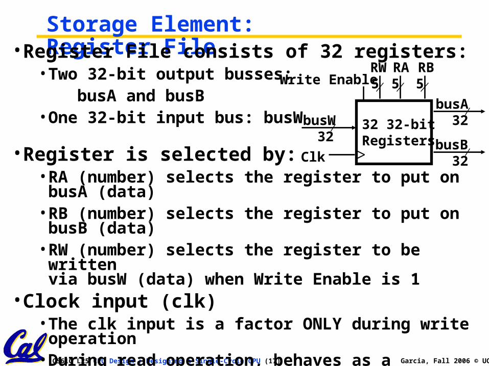
Storage Element: Register File• Register File consists of 32 registers:
• Two 32-bit output busses: busA and busB• One 32-bit input bus: busW
• Register is selected by:• RA (number) selects the register to put on busA (data)• RB (number) selects the register to put on busB (data)• RW (number) selects the register to be written
via busW (data) when Write Enable is 1• Clock input (clk)
• The clk input is a factor ONLY during write operation• During read operation, behaves as a combinational
logic block: RA or RB valid busA or busB valid after “access time.”
Clk
busW
Write Enable
3232
busA
32busB
5 5 5RWRA RB
32 32-bitRegisters

CS61C L25 CPU Design : Designing a Single-Cycle CPU (18) Garcia, Fall 2006 © UCB
Step 3: Assemble DataPath meeting requirements
• Register Transfer Requirements Datapath Assembly
• Instruction Fetch
• Read Operands and Execute Operation

CS61C L25 CPU Design : Designing a Single-Cycle CPU (19) Garcia, Fall 2006 © UCB
3a: Overview of the Instruction Fetch Unit
• The common RTL operations• Fetch the Instruction: mem[PC]• Update the program counter:
Sequential Code: PC PC + 4 Branch and Jump: PC “something else”
32
Instruction WordAddress
InstructionMemory
PCclk
Next AddressLogic

CS61C L25 CPU Design : Designing a Single-Cycle CPU (20) Garcia, Fall 2006 © UCB
3b: Add & Subtract• R[rd] = R[rs] op R[rt] Ex.: addU rd,rs,rt
• Ra, Rb, and Rw come from instruction’s Rs, Rt, and Rd fields
• ALUctr and RegWr: control logic after decoding the instruction
32Result
ALUctr
clk
busW
RegWr
32
32
busA
32
busB
5 5 5
Rw Ra Rb
32 32-bitRegisters
Rs RtRd
AL
U
op rs rt rd shamt funct061116212631
6 bits 6 bits5 bits5 bits5 bits5 bits
Already defined the register file & ALU

CS61C L25 CPU Design : Designing a Single-Cycle CPU (21) Garcia, Fall 2006 © UCB
Peer Instruction
A. Our ALU is a synchronous device
B. We should use the main ALU to compute PC=PC+4
C. The ALU is inactive for memory reads or writes.
ABC1: FFF2: FFT3: FTF4: FTT5: TFF6: TFT7: TTF8: TTT

CS61C L25 CPU Design : Designing a Single-Cycle CPU (22) Garcia, Fall 2006 © UCB
How to Design a Processor: step-by-step• 1. Analyze instruction set architecture (ISA)
datapath requirements• meaning of each instruction is given by the register transfers
• datapath must include storage element for ISA registers
• datapath must support each register transfer• 2. Select set of datapath components and establish clocking methodology
• 3. Assemble datapath meeting requirements• 4. Analyze implementation of each instruction to determine setting of control points that effects the register transfer.
• 5. Assemble the control logic (hard part!)