cs 61c: great ideas in computer architecture lecture 14: caches, part i instructor: sagar karandikar...
TRANSCRIPT

1
CS 61C: Great Ideas in Computer Architecture
Lecture 14: Caches, Part I
Instructor: Sagar [email protected]
http://inst.eecs.berkeley.edu/~cs61c
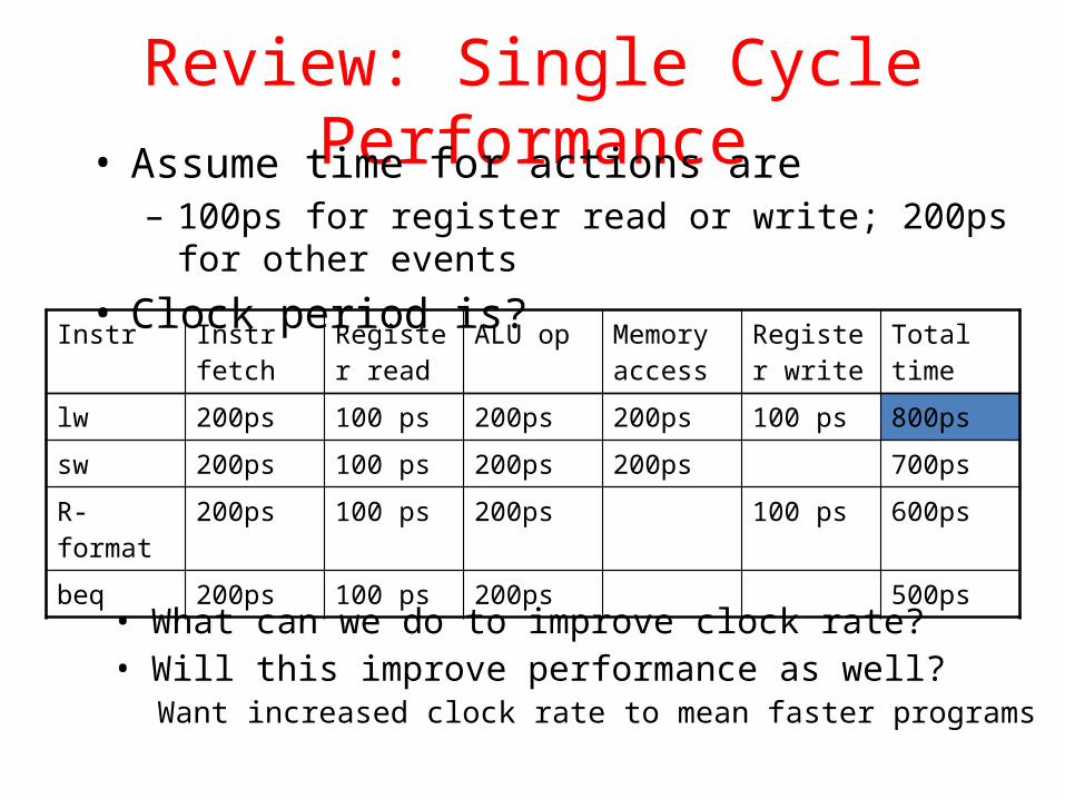
Review: Single Cycle Performance• Assume time for actions are
– 100ps for register read or write; 200ps for other events
• Clock period is?Instr Instr fetch Register
readALU op Memory
accessRegister write
Total time
lw 200ps 100 ps 200ps 200ps 100 ps 800ps
sw 200ps 100 ps 200ps 200ps 700ps
R-format 200ps 100 ps 200ps 100 ps 600ps
beq 200ps 100 ps 200ps 500ps
• What can we do to improve clock rate?• Will this improve performance as well?
Want increased clock rate to mean faster programs

3

4
Review: Pipelining Performance
Single-cycleTc = 800 psf = 1.25GHz
PipelinedTc = 200 ps
f = 5GHz

5
Review: Pipelining Hazards
A hazard is a situation that prevents starting the next instruction in the next clock cycle
1) Structural hazard– A required resource is busy
(e.g. needed in multiple stages)2) Data hazard
– Data dependency between instructions– Need to wait for previous instruction to complete
its data read/write3) Control hazard
– Flow of execution depends on previous instruction

6
Review: Resolving Control Hazards
• Jumps would require inserting one bubble (since we don’t know the jump immediate until decode)– Jump delay slot lets us put a useful instruction
here• Branches would require inserting two bubbles
(since we don’t do the equality comparison until the ALU stage)– Move equality comparison to decode stage, add
branch delay slot

Example: Nondelayed vs. Delayed Jump
add $1, $2, $3
sub $4, $5, $6
jal Foo
or $8, $9, $10
xor $10, $1, $11
Nondelayed Jumpadd $1, $2,$3
sub $4, $5, $6
jal Foo
or $8, $9, $10
xor $10, $1, $11
Delayed Jump
Foo: Foo:
$ra set to addr of xor: PC+4
$ra set to addr of xor: PC+8

8
Review: Resolving (many) Data Hazards: Forwarding
• Forward result as soon as it is available– OK that it’s not stored in RegFile yet
sub $t4,$t0,$t3A
LUI$ Reg D$ Reg
and $t5,$t0,$t6
AL
UI$ Reg D$ Reg
or $t7,$t0,$t8 I$
AL
UReg D$ Reg
xor $t9,$t0,$t10
AL
UI$ Reg D$ Reg
add $t0,$t1,$t2IF ID/RF EX MEM WBA
LUI$ Reg D$ Reg

9
Review: Structural Hazard #1: Registers
I$
Load
Instr 1
Instr 2
Instr 3
Instr 4
AL
U I$ Reg D$ Reg
AL
U I$ Reg D$ RegA
LU I$ Reg D$ Reg
AL
UReg D$ Reg
AL
U I$ Reg D$ Reg
Instr
Order
Time (clock cycles)
Can we read and write to registers simultaneously?

Review: Solving Regfile Structural Hazard: Double Pumping (2/3)
10
* This is not how registers work in general!
Capture value at this (falling) edge
Can read the new value here

11
Review: Structural Hazard #2: Single Memory
• MIPS pipeline with a single memory?– Load/Store requires memory access for data– Instruction fetch would have to stall for that cycle
• Causes a pipeline “bubble”
• Hence, pipelined datapaths require separate instruction/data memories– Separate L1 I$ and L1 D$ take care of this

12
I$
Load
Instr 1
Instr 2
Instr 3
Instr 4
AL
U I$ Reg D$ Reg
AL
U I$ Reg D$ RegA
LU I$ Reg D$ Reg
AL
UReg D$ Reg
AL
U I$ Reg D$ Reg
Instr
Order
Time (clock cycles)
Review: Structural Hazard #2: Single Memory
Trying to read same memory twice in same clock cycle

Review: Solving Structural Hazard #2 with Caches
13
Today, we’ll add caches

14
New-School Machine Structures(It’s a bit more complicated!)
• Parallel RequestsAssigned to computere.g., Search “Katz”
• Parallel ThreadsAssigned to coree.g., Lookup, Ads
• Parallel Instructions>1 instruction @ one timee.g., 5 pipelined instructions
• Parallel Data>1 data item @ one timee.g., Add of 4 pairs of words
• Hardware descriptionsAll gates @ one time
• Programming Languages
SmartPhone
Warehouse Scale
Computer
Software Hardware
HarnessParallelism &Achieve HighPerformance
Logic Gates
Core Core…
Memory (Cache)
Input/Output
Computer
Cache Memory
Core
Instruction Unit(s) FunctionalUnit(s)
A3+B3A2+B2A1+B1A0+B0
How dowe know?

15
Processor
Control
Datapath
Components of a Computer
PC
Registers
Arithmetic & Logic Unit(ALU)
MemoryInput
Output
Bytes
Enable?Read/Write
Address
Write Data
ReadData
Processor-Memory Interface I/O-Memory Interfaces
Program
Data

Processor-DRAM Gap (latency)
16
Time
µProc 60%/year
DRAM7%/year
1
10
100
100019
8019
81
1983
1984
1985
1986
1987
1988
1989
1990
1991
1992
1993
1994
1995
1996
1997
1998
1999
2000
DRAM
CPU
1982
Processor-MemoryPerformance Gap:(growing 50%/yr)
Perf
orm
ance
1980 microprocessor executes ~one instruction in same time as DRAM access2015 microprocessor executes ~1000 instructions in same time as DRAM access

17
Big Idea: Memory HierarchyProcessor
Size of memory at each level
Increasing distance from
processor,decreasing
speed
Level 1
Level 2
Level n
Level 3
. . .
Inner
Outer
Levels in memory hierarchy
As we move to outer levels the latency goes up and price per bit goes down. Why?

18
Library Analogy
• Writing a report based on books on reserve– E.g., works of J.D. Salinger
• Go to library to get reserved book and place on desk in library
• If need more, check them out and keep on desk– But don’t return earlier books since might need them
• You hope this collection of ~10 books on desk enough to write report, despite 10 being only 0.00001% of books in UC Berkeley libraries

19
Administrivia
• HW3 Out• Proj2-2 Out• Midterm regrades due today @ 23:59:59• Register your Project 3 Teams

20
In the News: RowHammer Exploit
• CMU + Intel researchers found commercial DRAM chips susceptible to neighboring bits flipping if one row of memory accessed frequently
• Google Engineers figured out how to use this to gain root access on a machine! Almost all laptops susceptible, but server ECC memory helps reduce impact.

21
Break

Real Memory Reference Patterns
Donald J. Hatfield, Jeanette Gerald: Program Restructuring for Virtual Memory. IBM Systems Journal 10(3): 168-192 (1971)
Time
Mem
ory
Addr
ess
(one
dot
per
acc
ess)

23
Big Idea: Locality
• Temporal Locality (locality in time)– Go back to same book on desktop multiple times– If a memory location is referenced, then it will tend to
be referenced again soon• Spatial Locality (locality in space)
– When go to book shelf, pick up multiple books on J.D. Salinger since library stores related books together
– If a memory location is referenced, the locations with nearby addresses will tend to be referenced soon

Memory Reference Patterns
Donald J. Hatfield, Jeanette Gerald: Program Restructuring for Virtual Memory. IBM Systems Journal 10(3): 168-192 (1971)
Time
Mem
ory
Addr
ess
(one
dot
per
acc
ess)
SpatialLocality
Temporal Locality

25
Principle of Locality
• Principle of Locality: Programs access small portion of address space at any instant of time
• What program structures lead to temporal and spatial locality in instruction accesses?
• In data accesses?

Memory Reference PatternsAddress
Time
Instruction fetches
Stackaccesses
Dataaccesses
n loop iterations
subroutine call
subroutine return
argument access
vector access
scalar accesses

27
Cache Philosophy• Programmer-invisible hardware mechanism to
give illusion of speed of fastest memory with size of largest memory– Works fine even if programmer has no idea what a
cache is– However, performance-oriented programmers
today sometimes “reverse engineer” cache design to design data structures to match cache
– We’ll do this in Project 4

28
Memory Access without Cache
• Load word instruction: lw $t0,0($t1)• $t1 contains 1022ten, Memory[1022] = 99
1. Processor issues address 1022ten to Memory
2. Memory reads word at address 1022ten (99)
3. Memory sends 99 to Processor4. Processor loads 99 into register $t0

29
Processor
Control
Datapath
Adding Cache to Computer
PC
Registers
Arithmetic & Logic Unit(ALU)
MemoryInput
Output
Bytes
Enable?Read/Write
Address
Write Data
ReadData
Processor-Memory Interface I/O-Memory Interfaces
Program
Data
Cache

30
Memory Access with Cache• Load word instruction: lw $t0,0($t1)• $t1 contains 1022ten, Memory[1022] = 99• With cache (similar to a hash)
1. Processor issues address 1022ten to Cache
2. Cache checks to see if has copy of data at address 1022ten
2a. If finds a match (Hit): cache reads 99, sends to processor2b. No match (Miss): cache sends address 1022 to Memory
I. Memory reads 99 at address 1022ten
II. Memory sends 99 to CacheIII. Cache replaces word with new 99IV. Cache sends 99 to processor
3. Processor loads 99 into register $t0

31
Cache “Tags”• Need way to tell if have copy of location in
memory so that can decide on hit or miss• On cache miss, put memory address of block
in “tag address” of cache block– 1022 placed in tag next to data from memory (99)
Tag Data
252 121022 99131 7
2041 20
From earlierinstructions

Anatomy of a 16 Byte Cache,
4 Byte Block
• Operations:1. Cache Hit2. Cache Miss3. Refill cache from
memory
• Cache needs Address Tags to decide if Processor Address is a Cache Hit or Cache Miss– Compares all 4 tags
32
Processor
32-bitAddress
32-bitData
Cache
32-bitAddress
32-bitData
Memory
1022 99252
720
12
1312041

33
Tag Data
252 12
1022 99
131 7
2041 20
Tag Data
252 121022 99511 11
2041 20
Cache Replacement• Suppose processor now requests location 511, which
contains 11?• Doesn’t match any cache block, so must “evict” one
resident block to make room– Which block to evict?
• Replace “victim” with new memory block at address 511

34
Block Must be Aligned in Memory
• Word blocks are aligned, so binary address of all words in cache always ends in 00two
• How to take advantage of this to save hardware and energy?
• Don’t need to compare last 2 bits of 32-bit byte address (comparator can be narrower)
=> Don’t need to store last 2 bits of 32-bit byte address in Cache Tag (Tag can be narrower)
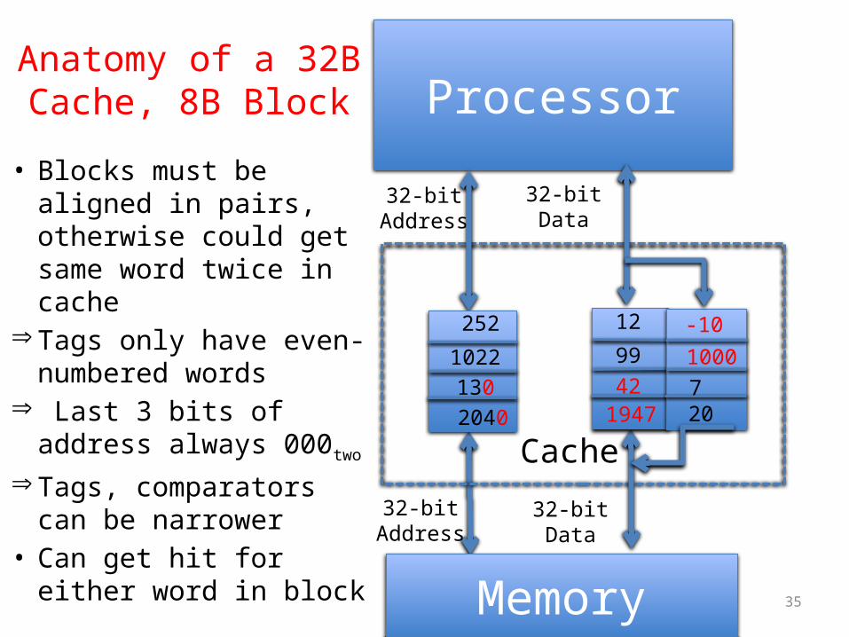
Anatomy of a 32B Cache, 8B Block
35
• Blocks must be aligned in pairs, otherwise could get same word twice in cache
Tags only have even-numbered words
Last 3 bits of address always 000two
Tags, comparators can be narrower
• Can get hit for either word in block
Processor
32-bitAddress
32-bitData
Cache
32-bitAddress
32-bitData
Memory
1022 99252
421947
12
1302040
1000720
-10

36
Hardware Cost of Cache
• Need to compare every tag to the Processor address
• Comparators are expensive
• Optimization: 2 sets => ½ comparators
• 1 Address bit selects which set
36
Processor
32-bitAddress
Tag Data
32-bitData
Cache
32-bitAddress
32-bitData
Memory
Tag Data
Set 0
Set 1

37
Processor Address Fields used by Cache Controller
• Block Offset: Byte address within block• Set Index: Selects which set• Tag: Remaining portion of processor address
• Size of Index = log2 (number of sets)• Size of Tag = Address size – Size of Index
– log2 (number of bytes/block)
Block offsetSet IndexTag
Processor Address (32-bits total)
38
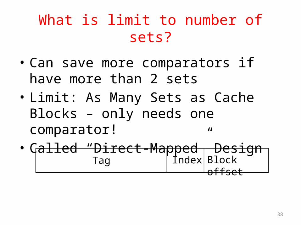
What is limit to number of sets?
• Can save more comparators if have more than 2 sets
• Limit: As Many Sets as Cache Blocks – only needs one comparator!
• Called “Direct-Mapped” Design
Block offsetIndexTag

39
Mapping a 6-bit Memory Address
• In example, block size is 4 bytes/1 word (it could be multi-word)• Memory and cache blocks are the same size, unit of transfer between memory and
cache• # Memory blocks >> # Cache blocks
– 16 Memory blocks/16 words/64 bytes/6 bits to address all bytes– 4 Cache blocks, 4 bytes (1 word) per block– 4 Memory blocks map to each cache block
• Byte within block: low order two bits, ignore! (nothing smaller than a block)• Memory block to cache block, aka index: middle two bits• Which memory block is in a given cache block, aka tag: top two bits
05 1
Byte Offset Within Block(e.g., Word)
23
Block Within $Index
4
Mem Block Within$ Block
Tag

40
One More Detail: Valid Bit
• When start a new program, cache does not have valid information for this program
• Need an indicator whether this tag entry is valid for this program
• Add a “valid bit” to the cache tag entry– 0 => cache miss, even if by chance, address = tag– 1 => cache hit, if processor address = tag

41
Caching: A Simple First Example
00011011
Cache
Main Memory
Q: Where in the cache is the mem block?
Use next 2 low-order memory address bits – the index – to determine which cache block (i.e., modulo the number of blocks in the cache)
Tag Data
Q: Is the memory block in cache?Compare the cache tag to the high-order 2 memory address bits to tell if the memory block is in the cache (provided valid bit is set)
Valid
0000xx0001xx0010xx0011xx0100xx0101xx0110xx0111xx1000xx1001xx1010xx1011xx1100xx1101xx1110xx1111xx
One word blocksTwo low order bits (xx) define the byte in the block (32b words)
Index

42
• One word blocks, cache size = 1K words (or 4KB)Direct-Mapped Cache Example
20Tag 10Index
Data Index TagValid012...
102110221023
31 30 . . . 13 12 11 . . . 2 1 0Block offset
What kind of locality are we taking advantage of?
20
Data
32
HitValid bit ensures
something useful in cache for this index
Compare Tag with
upper part of Address to see if a Hit
Readdata from cache
instead of
memory if a Hit
Comparator

43
• Four words/block, cache size = 1K words
Multiword-Block Direct-Mapped Cache
8Index
DataIndex TagValid012...
253254255
31 30 . . . 13 12 11 . . . 4 3 2 1 0 Byte offset
20
20Tag
Hit Data
32
Block offset
What kind of locality are we taking advantage of?

44
Cache Names for Each Organization
• “Fully Associative”: Block can go anywhere– First design in lecture– Note: No Index field, but 1 comparator/block
• “Direct Mapped”: Block goes one place – Note: Only 1 comparator– Number of sets = number blocks
• “N-way Set Associative”: N places for a block– Number of sets = number of blocks / N– Fully Associative: N = number of blocks– Direct Mapped: N = 1

45
Range of Set-Associative Caches• For a fixed-size cache, each increase by a factor of 2 in
associativity doubles the number of blocks per set (i.e., the number of “ways”) and halves the number of sets – • decreases the size of the index by 1 bit and
increases the size of the tag by 1 bit
Block offsetIndexTag
More Associativity (more ways)
Note: IBM persists in calling sets “ways” and ways “sets”.They’re wrong.

46
Clickers/Peer Instruction
• For a cache with constant total capacity, if we increase the number of ways by a factor of 2, which statement is false:
• A: The number of sets could be doubled• B: The tag width could decrease• C: The number of tags could stay the same• D: The block size could be halved• E: Tag width must increase

47
Break

48
Second-LevelCache
(SRAM)
Typical Memory Hierarchy
Control
Datapath
SecondaryMemory
(DiskOr Flash)
On-Chip Components
RegFile
MainMemory(DRAM)D
ataCache
InstrCache
Speed (cycles): ½’s 1’s 10’s 100’s 1,000,000’s
Size (bytes): 100’s 10K’s M’s G’s T’s
• Principle of locality + memory hierarchy presents programmer with ≈ as much memory as is available in the cheapest technology at the ≈ speed offered by the fastest technology
Cost/bit: highest lowest
Third-LevelCache
(SRAM)

49
Handling Stores with Write-Through
• Store instructions write to memory, changing values
• Need to make sure cache and memory have same values on writes: 2 policies
1) Write-Through Policy: write cache and write through the cache to memory– Every write eventually gets to memory– Too slow, so include Write Buffer to allow processor to
continue once data in Buffer– Buffer updates memory in parallel to processor

Write-Through Cache
• Write both values in cache and in memory
• Write buffer stops CPU from stalling if memory cannot keep up
• Write buffer may have multiple entries to absorb bursts of writes
• What if store misses in cache?
50
Processor
32-bitAddress
32-bitData
Cache
32-bitAddress
32-bitData
Memory
1022 99252
7
20
12
1312041 Addr Data
Write Buffer

51
Handling Stores with Write-Back
2) Write-Back Policy: write only to cache and then write cache block back to memory when evict block from cache– Writes collected in cache, only single write to
memory per block– Include bit to see if wrote to block or not, and
then only write back if bit is set• Called “Dirty” bit (writing makes it “dirty”)

Write-Back Cache
• Store/cache hit, write data in cache only & set dirty bit– Memory has stale value
• Store/cache miss, read data from memory, then update and set dirty bit– “Write-allocate” policy
• Load/cache hit, use value from cache
• On any miss, write back evicted block, only if dirty. Update cache with new block and clear dirty bit.
52
Processor
32-bitAddress
32-bitData
Cache
32-bitAddress
32-bitData
Memory
1022 99252
7
20
12
1312041
DDDD
Dirty Bits

53
Write-Through vs. Write-Back
• Write-Through:– Simpler control logic– More predictable timing
simplifies processor control logic
– Easier to make reliable, since memory always has copy of data
• Write-Back– More complex control logic– More variable timing (0,1,2
memory accesses per cache access)
– Usually reduces write traffic
– Harder to make reliable, sometimes cache has only copy of data
54
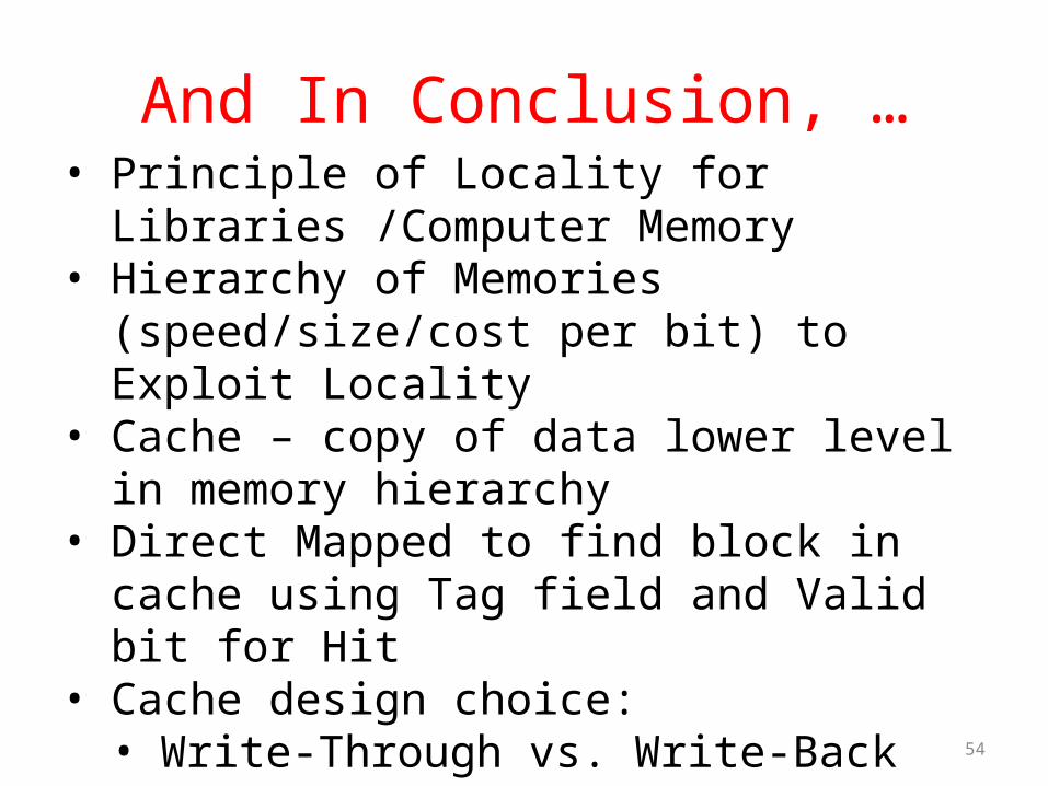
And In Conclusion, …• Principle of Locality for Libraries /Computer
Memory• Hierarchy of Memories (speed/size/cost per
bit) to Exploit Locality• Cache – copy of data lower level in memory
hierarchy• Direct Mapped to find block in cache using Tag
field and Valid bit for Hit• Cache design choice:
• Write-Through vs. Write-Back