course number section - concordia universityusers.encs.concordia.ca/~rabinr/web_elec_311/past...
TRANSCRIPT

Course Number Section Electronics I ELEC 311 BB Examination Date Time # of pages Final August 12, 2005 Three hours 3 Instructor Dr. R. Raut M ateria ls a llow ed : N o Y es (P lease sp ecify) C alcu lato rs a llow ed : N o Y es
X
X
Students are allowed to use silent, non-programmable electronic calculators without text display. Special Instructions: Attempt all questions. Show all steps clearly in neat and legible handwriting. Students are required to return question paper together with exam booklet(s).
Q.1: For the equivalent circuit below, find the corresponding basic voltage amplifier model, i.e., find (a) AVO = vo/vi, (ii) Ri , and (iii) Ro. Now find the corresponding transconductance model equivalent for the same circuit.
iv
ov
10
110 5
ii20 i2
ii
ioi
iR oR
oi2
Q.2: A zener diode exhibits a constant voltage of 5.6 V for currents greater than five times than the knee current IZK=0.5 mA. The zener is used to build a shunt regulator fed from a raw DC supply with nominal value of 15 V. The load current varies from 0 mA to 15 mA. Find a suitable value for the resistance R which is connected in series with the raw DC supply. The zener has an internal resistance of 5 ohms. What will be the load regulation of this regulator system?

Q.3: A semiconductor junction diode is used in an automatic gain control system as shown below. The ac resistance of the diode is dependent on the amplitude Vp of the input signal. Higher Vp is, lower is the diode ac resistance and more it tends to attenuate the input ac signal. That is how the gain control mechanism works. The input signal is half-wave rectified to generate a DC voltage which drives the DC current through the diode. This DC voltage is given by /pV . The diode is a 1 mA diode. The voltage drop across the diode changes by
100 milli volts for a decade (10 times) change in current through it. You may use the relation: )/log(303.2 1212 IInVVV T . The DC resistance of the diode can be neglected.
(a) If the input ac signal has an amplitude of 15 volts, what will be the output signal magnitude vo? (b) If the input ac signal amplitude shoots up to 30 volts, how much (approximately) will vo become?
)()( tSinVtv p
DCV
Cov
Q.4: Design the following BJT circuit to obtain a dc current of 1 mA and to ensure a ±2 V signal swing at the collector; that is design for VCE =2.3 V. Given that VCC=10 V, and β = 100.
CCV
CR
BR

Q.5: Consider the emitter-follower BJT amplifier circuit below. Find Rin, Rout and the voltage gain vo/vsig. Given Rsig = 10 kΩ, RB = 40 kΩ, RL = 1 kΩ, β=49, and VA = 100 V. The bias current I = 5 mA. What is the largest peak amplitude of an output sine-wave signal that can be used without the transistor cutting off?
CCV
sigv
sigR
1C
2C
BRLR
I
EEVinR
outR
ov
Q.6: (a) Consider the MOS circuit below. The transistor Q1 is biased for ID = 80 μA. Both Q1 and Q2 have Vt=0.6 V. Design R and then find the drain current and drain voltage for Q2. The channel modulation effect may be ignored and you may use the I-V equation: 2( )ni GS tI K V V , i=1,2 for your work. Given
2 21 2500 / , 750 /n nK A V K A V for transistors Q1 and Q2 respectively.
(b) Assume now that the early voltage VA = 40 V for both Q1 and Q2. Draw the ac equivalent model for the circuit below.
R
3DDV V
2 20R k
1Q2Q

Course Number Section Electronics I ELEC 311 BB Final Examination Date Time # of pages August 22, 2006 Three hours 4 Instructor Dr. R. Raut M ateria ls a llow ed : N o Y es (P lease sp ecify) C alcu lato rs a llow ed : N o Y es
X
X
Students are allowed to use silent, non-programmable electronic calculators without text display. Special Instructions: Attempt all questions. Show all steps clearly in neat and legible handwriting. Students are required to return question paper together with exam booklet(s).
Q.1: For the circuit shown below, find ID and VD for the case VDD =5 V, and R= 10 k . Assume that the diode has a voltage drop of 0.7 V at 1-mA current and that the voltage changes by 0.1 V/decade of current change. Use (a) iteration method, and (b) the piecewise-linear model for the diode with VDO=0.65 V and rD =20 .
Figure 1
Q.2: A bridge-rectifier circuit with a filter capacitor has R= 100 ohms. The secondary transformer delivers a sinusoid of 12 V (rms) and has a frequency of 60 Hz. The diodes have VD = 0.8 V each. (a) What will be the value of the filter capacitor so that the ripple voltage is limited to below 0.5 V peak-to-peak?

(b) What is the DC voltage at the output of the system? (c) What is the conduction angle for the diode? Q.3: For the transistor amplifier shown below, assume 1 and VBE =0.5 V at the edge of conduction. (a) What are the values of VE and VC for VB =0 V? (b) For what value of VB does the transistor cut off?, Saturate? (c) In each case, what values of VE and VC result?
Figure 3
Q.4: For the BJT circuit below, the signal source generates ac signal with zero DC. The transistor has =100, and ro =200 k . (a) Find RE to establish a DC current of 0.5 mA. Assume VBE=0.7 V for conduction. (b) Find RC to obtain VC = 5 V. (c) With RL = 10 k , draw the ac equivalent circuit for the amplifier system, and (d) Determine the system voltage gain.
Figure 4

Q.5: For the circuit shown below, find (a) the input resistance Rin , and (b) the voltage gain vo/vsig . Assume that the source provides a small signal vsig and that =100. (c)What will be the maximum vsig value for which the small signal approximation will remain valid?
Figure 5
Q.6: Consider the MOSFET amplifier in the figure below. Given that VG= 4V, RS=1
k . The transistor has Vt= 1V, and ( / )nk W L = 2 mA/V2 .
(a) Find the bias current ID? (b) What will be the voltage gain vo/vsig, if RD =20 k , RG1 = 2 M , RG2 =1 M , Rsig =10 k , and VDD =12 V?
Figure 6

Some important Formulas (BJT & MOSFET)

Course Number Section Electronics I ELEC 311 BB Final Examination Date Time # of pages August 15, 2007 Three hours 4 Instructor Dr. R. Raut M aterials a llow ed : N o Y es (P lease sp ecify) C alcu lato rs a llow ed : N o Y es
X
X
Students are allowed to use silent, non-programmable electronic calculators without text display. Special Instructions: Attempt all questions. Show all steps clearly in neat and legible handwriting. Students are required to return question paper together with exam booklet(s).
Q.1: For the equivalent circuit below, find the corresponding basic voltage amplifier model, i.e., find (a) AVO = vo/vi, (ii) Ri , and (iii) Ro.
iv
ov
10
110 5
ii20 i2
ii
ioi
iR oR
oi2
Figure 1
Q.2: A semiconductor junction diode is used in an automatic gain control system as shown below. The ac resistance of the diode is dependent on the amplitude Vp of the input signal. Higher Vp is, lower is the diode ac resistance and more it tends to attenuate the input ac signal. That is how the gain control mechanism works.

)()( tSinVtv p
DCV
Cov
Figure 2
The input signal is half-wave rectified to generate a DC voltage which drives the DC current through the diode. This DC voltage VDC is given by /pV , where Vp is the
amplitude of the ac signal. The diode is a 1 mA diode. The voltage drop across the diode changes by 100 milli volts for a decade (10 times) change in current through it. You may use the relation
)/log(303.2 1212 IInVVV T . The DC resistance of the diode can be neglected.
(a) If the input ac signal has an amplitude of 15 volts, what will be the amplitude of the output signal vo?
(b) If the input ac signal amplitude shoots up to 30 volts, how much will vo become?
Q.3: For the transistor amplifier shown below, assume 1 and VBE =0.5 V at the edge of conduction. (a) What are the values of VE and VC for VB =0 V? (b) For what value of VB does the transistor cut off?, Saturate? (c) In each case, what values of VE and VC result?

Figure 3 Q.4: For the circuit shown below, find (a) the input resistance Rin , and (b) the voltage gain vo/vsig . Assume that the source provides a small signal vsig and that =100. (c)What will be the maximum vsig value for which the small signal approximation will remain valid?
Figure 4
Q.5: Consider the MOSFET amplifier in the figure below. Given that VG= 4V, RS-
=1 k . The transistor has Vt= 1V, and ( / )nk W L = 2 mA/V2 . (a) Find the bias current ID? (b) What will be the voltage gain vo/vsig, if RD =20 k , RG1 = 2 M , RG2 =1 M , Rsig =10 k , and VDD =12 V?
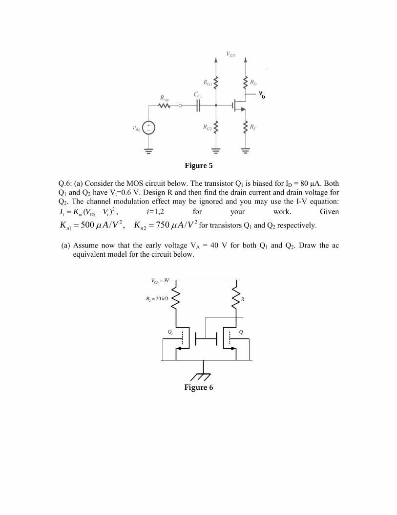
Figure 5
Q.6: (a) Consider the MOS circuit below. The transistor Q1 is biased for ID = 80 μA. Both Q1 and Q2 have Vt=0.6 V. Design R and then find the drain current and drain voltage for Q2. The channel modulation effect may be ignored and you may use the I-V equation:
2( )i ni GS tI K V V , i=1,2 for your work. Given 2 2
1 2500 / , 750 /n nK A V K A V for transistors Q1 and Q2 respectively.
(a) Assume now that the early voltage VA = 40 V for both Q1 and Q2. Draw the ac
equivalent model for the circuit below.
R
3DDV V
2 20R k
1Q2Q
Figure 6
Course Number Section Electronics I ELEC 311 BB Examination Date Time # of pages
Final August 20, 2008 3 hours 4 Instructor(s) R. Raut
M aterials a llow ed : N o Y es (P lease sp ecify) C alcu lato rs a llow ed : N o Y es
X
X
Students are allowed to use ENCS approved calculators only. Special Instructions: Attempt ALL questions. Show all steps clearly in neat and legible handwriting. Students are required to return question paper together with exam booklet(s).
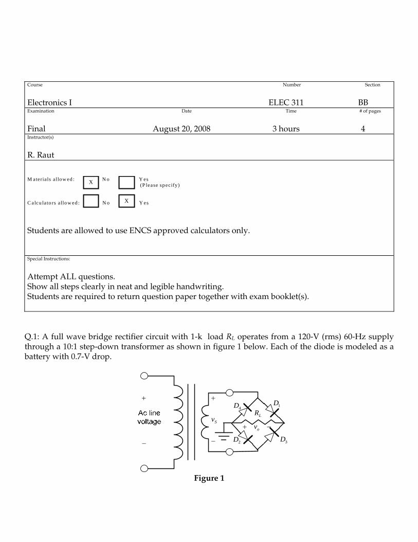
Q.1: A full wave bridge rectifier circuit with 1-k load RL operates from a 120-V (rms) 60-Hz supply through a 10:1 step-down transformer as shown in figure 1 below. Each of the diode is modeled as a battery with 0.7-V drop.
_
Sv
1D
2D 3D
4DLR
ov
Figure 1

(a) What is the peak value of the rectified voltage across the load? (b) For what fraction of a cycle does each diode conduct? (c ) What is the average current through the load? Q.2: For the circuit shown in figure 2, the voltage VE was measured to be -0.7 V. If =50, find IE, IB, IC, and VC.
V10
k5
V10
k10
CV
EV
CI
EI
BI
Figure 2
Q.3: In the circuit shown below (Fig.3), the transistor has =199. Find
sv
k1
k10
mA10
100
V5.1
V5
C
Cbv
ov
inR ibR
Figure 3 (a) the DC voltage at the collector. (b) the DC voltage at the base (c) the input resistance Rin (use the small-signal ac equivalent circuit model for the BJT)

Q.4: In the BJT amplifier circuit of figure 4, the DC bias current IC is 2.3 mA. The transistor has a =100 and Early voltage VA =100 Volts.
sv
ov
V10
k3
k100
Figure 4
(a) Draw the small-signal ac equivalent model for the amplifier and show the values of the ac parameters gm, rπ, ro.
(b) Find the voltage gain vo/vs. (c) Up to what value of vs the amplifier will operate properly (i.e., the BJT shall remain in the active
mode)? Q.5: Consider the MOFET amplifier shown in figure 5. Design the resistances so that you can achieve VD=3.4 V, VS =1.6 V, and ID=0.3 mA. The voltage divider resistances RG1, RG2 has a current of 1-A. The MOSFET has Vt=1 V, )/( Lwkn 1 mA/V2.
DDV
1GR
2GR
DR
SR
Figure 5
Q.6: For the NMOS amplifier shown in figure 6, replace the transistor with its T-equivalent model. Derive (a) the expression for the voltage gain vs/vi. (b) the expression for the voltage gain vd/vi.

VVDD 10
DR
SR
iv
dv
sv
Figure 6
(Some formulae and equivalent circuits)
BC II , BE II )1(
T
Cm V
Ig ,
mgr
,
1
C
Ao I
Vr ,
1
rre ,
)/exp( TBESC VVII
2)(
2DS
DStGSD
VVVV
L
WkI
(linear region)
)1(2
2DStGSD VVV
L
WkI
(saturation region)
L
WkIVV
L
Wkg D
tGsm
2
D
Ao I
Vr
r or
vvgm
BJT hybrid pi
eror
ei
ei
BJT T
orgsmvg
gsv
MOS hybrid pi
mg/1
orgsmvg
gsv
MOS T

Course Number Section
Electronics I ELEC 311/1 BB Examination Date Time # of pages
Final August 14, 2009 3 hours 6 Instructor(s)
Dr.R. Raut
M aterials a llow ed : N o Y es (P lease sp ec ify) C alcu lato rs a llow ed : N o Y es
X
X
Students are allowed to use ENCS faculty approved calculators
Special Instructions:
You MUST attempt Q.1 (soft skill component) .
For Q.2‐Q.7, answer any FOUR questions.
Before submitting your answer book, fill in the Table below indicating the answers you want to be graded.
If you do not fill in the Table, the instructor will mark your answers as they appear one after another in the answer
book
Show all steps clearly in neat and legible handwriting.
Students are required to return the question paper together with exam booklet(s).
Table
Answers to be graded
Q.1 (compulsory)
Marks

(Soft skill component- The student MUST answer this question)
Q.1: Consider the MOS circuit below. Both Q1 and Q2 have Vt=0.7 V. Ignore the channel
modulation effect. You may use the I-V equation: 2( )ni GS tI K V V , i=1,2 for your work.
Given 2 21 2500 / , 750 /n nK A V K A V for transistors Q1 and Q2 respectively.
(a) Design R to establish ID = 100 μA in the transistor Q1
(b) Find the drain current and drain voltage for Q2.
R
3DDV V
2 20R k
1Q2Q
Figure 1:
(Answer any FOUR from the questions below)
Q.2: A zener diode exhibits a voltage of 6.5 V for IZ= 5 mA. The zener has IZK=0.5 mA, and a minimum of five times IZK must flow through the zener for reliable operation. The diode has an internal resistance of 15 ohms. The device is used to build a shunt regulator circuit as shown below.
The raw DC supply has a nominal value of 15 V, and can range between 12 V to 18 V. The load current varies from 0 mA to 15 mA.
R
LRSV
OZ VV
LI
Figure 2:

(a) Design a suitable value for the resistance R for reliable operation. (b) What will be the output voltage if RL= 450 Ω is connected across the output of the
system and the raw DC is at its lowest value (12 V)?
Q.3: A bridge-rectifier circuit with a filter capacitor has RL = 100 ohms. The secondary transformer delivers a sinusoid of 15 V (rms) and has a frequency of 60 Hz. The diodes have VDO = 0.7 V each.
Figure 3
(a) What will be the value of the filter capacitor C so that the ripple voltage is limited to below 500 mV peak-to-peak?
(b) What is the DC voltage at the output of the system?
(c) What is the conduction angle for each diode in the system? Explain with appropriate sketches.
Q.4: For the BJT circuit (Figure 4), the signal source generates ac signal with zero DC. The transistor has =100, and ro =20 k .
(a) Find RE to establish a DC current of IE= 0.5 mA. Assume VBE=0.7 V for conduction.
(b) Find RC to obtain VC = 5 V.
(c) Determine the system voltage gain with RL = 10 k ,
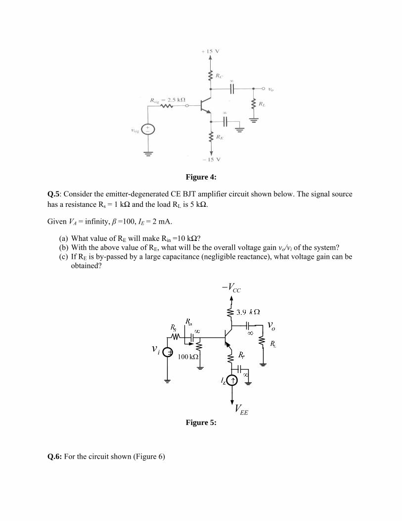
Figure 4:
Q.5: Consider the emitter-degenerated CE BJT amplifier circuit shown below. The signal source has a resistance Rs = 1 kΩ and the load RL is 5 kΩ.
Given VA = infinity, β =100, IE = 2 mA.
(a) What value of RE will make Rin =10 kΩ? (b) With the above value of RE, what will be the overall voltage gain vo/vi of the system? (c) If RE is by-passed by a large capacitance (negligible reactance), what voltage gain can be
obtained?
iv
ov
k 100
CCV
EEV
Figure 5:
Q.6: For the circuit shown (Figure 6)

(a) Draw the ac equivalent circuit for the amplifier.
(b) Find the voltage gain vo/vsig . Assume that the source provides a small signal vsig with zero DC., and that =100.
(c)What will be the maximum vsig value for which the small signal approximation will remain valid?
Figure 6:
Q.7: Consider the MOSFET amplifier in the figure below. Given that VG= 4V VDD =10 V, RS=1
k . The transistor has Vt= 1V, and ( / )nk W L = 5 mA/V2 .
(a) Find the bias current ID through the MOS device.
(b) What will be the voltage gain vo/vsig, if RD =15 k , RG1 = 2 M , RG2 =1 M ,Rsig =10 kΩ?
Figure 7:

Some important Formulas (BJT & MOSFET)

Course Number Section
Electronics I ELEC 311/1 BB Examination Date Time # of pages
Final August 17, 2012 3 hours 6 Instructor(s) Dr.R. Raut
M ateria ls a llow ed : N o Y es (P lease sp ec ify) C alcu lato rs a llow ed : N o Y es
X
X
Students are allowed to use ENCS faculty approved calculators Special Instructions: You MUST attempt Q.1 (soft skill component) . For Q.2-Q.8, answer any FIVE questions. Before submitting your answer book, fill in the Table below indicating the answers you want to be graded. If you do not fill in the Table, the instructor will mark your answers as they appear one after another in the answer book Show all steps clearly in neat and legible handwriting. Students are required to return the question paper together with exam booklet(s).
Table (Do not forget to fill in!)
Answers to be graded
Q.1 (compulsory)
Marks

(Soft skill component- The student MUST answer this question) Q.1: Figure 1 depicts two NMOS transistors each with VTHN =0.5 V, Kn =0.5 mA/V2, and W/L ratio of 4. The early voltage for M2 can be assumed to be infinity.
1R2R
GV
1DV
Figure 1
(a) Design R1 so that VG =0.7 V. (b) Find R2 so that M1 will be just at the edge of saturation region. (c) What will be the current in M1 if it has an early voltage of 50 V?
(Answer any FIVE questions)
Q.2: A semiconductor junction diode D is used in an automatic gain control system as shown in figure 2. The ac resistance of the diode is dependent on the amplitude Vp of the input signal. The capacitance acts as a short circuit and the inductor acts as an open circuit for the ac signal. The input signal is full-wave rectified to generate a DC voltage which drives the DC current through the diode. This DC voltage is given by 2 /pV . The diode is a 1 mA diode. The voltage
drop across the diode changes by 100 milli volts for a decade (10 times) change in current through it. For the diode you may use the relation: )/(log303.2 121012 IInVVV T , where VT is
the thermal voltage (=25 mV). The DC resistance of the diode can be neglected. If the input ac signal has a peak amplitude of 10 volts, what will be the output signal magnitude vo?

2.5k
L
Figure 2 Q.3: The bridge-rectifier circuit in figure 3 with a filter capacitor has RL= 200 ohms. The secondary transformer delivers a sinusoid of 15 V (rms) and has a frequency of 60 Hz. The diodes have VD = 0.8 V each. (a) What will be the value of the filter capacitor so that the ripple voltage is limited to below 0.5 volts peak-to-peak? (b) What is the DC voltage at the output of the system? (c) What should be the PIV rating for the diodes?
Figure 3

Q.4: Calculate the small signal gain vo/vs for the BJT amplifier circuit in figure 4. Assume transistor parameters of β = 80, VBE (on) = 0.7 V, VA = 50V.
50k
3k
Figure 4
Q.5: Design (i.e., design the resistor values) a bias-stable PNP-BJT amplifier stage of figure 5 to meet the following specifications. The transistor Q-point values are to be: VECQ = 6 V, ICQ ≈ 0.5 mA and VRE ≈ 2 V. Assume transistor parameters of β = 99 and VBE (ON) = 0.7 V.
Figure 5
Find R1, R2, RE, and RC.

Q.6: For the circuit shown in figure 6 find (a) the input resistance Rin , and (b) the voltage gain vo/vs . Assume that the source provides a small signal vsig and that =100. (c) What will be the maximum vs value for which the small signal approximation will remain valid?
100k 2.2k
C
0.5mA
C
sv
60
ov
inR
Figure 6
Q.7: A Common Source (CS) MOSFET amplifier is biased at ID =0.25 mA with a current source connected at the Source terminal of the MOSFET. The transistor has VOV =0.3 V, and a drain resistance of RD =15 kΩ connected to the DC supply of 15 V. The device has VA =50 V. The amplifier is capacitively fed from a source with internal resistance Rsig =100 kΩ, and a 20 kΩ load is capacitively coupled to the drain of the amplifier.
(a) Draw the schematic for the amplifier system. (b) Calculate the voltage gain of the system.
Q.8: Consider figure 8. Calculate the labeled node voltages V1 and V2, given that the MOSFETs
have VTHN =1 V, and 23 mA/Vn
WK
L .

1 k
1V
2V
Figure 8
(Some formulae and equivalent circuits)
BC II , BE II )1(
T
Cm V
Ig ,
mgr
,
1
C
Ao I
Vr ,
1
rre ,
)/exp( TBESC VVII
2)(
2DS
DStGSD
VVVV
L
WkI
(linear region)
)1(2
2DSTHGSD VVV
L
WkI
(saturation region)
L
WkIVV
L
Wkg D
THGsm
2
D
Ao I
Vr
r or
vvgm
BJT hybrid pi
eror
ei
ei
BJT T
orgsmvg
gsv
MOS hybrid pi
mg/1
orgsmvg
gsv
MOS T

of
Course Number Section
Electronics I ELEC 311/2 F,U Examination Date Time # of pages
Final December 13, 2012 3 hours 8 Instructor(s)
Dr.R. Raut, Dr. V. Ramachandran
M ateria ls a llo w ed : N o Y es (P lease sp ec ify) C alcu lato rs a llo w ed : N o Y es
X
X
Students are allowed to use ENCS faculty approved calculators
Special Instructions:
You are required to answer SIX questions
You MUST attempt Q.1 (soft skill component) : 6 marks
From Q.2‐Q.6, answer any THREE questions.: 8 marks (each)
From Q.7‐Q.10 answer any TWO questions: 10 marks (each)
Before submitting your answer book, fill in the Table below indicating the answers you want to be graded.
(If you do not fill in the Table, the instructor will mark your answers as they appear one after another in the answer
book)
Show all steps clearly in neat and legible handwriting.
Students are required to return the question paper together with exam booklet(s).
(STUDENT) NAME: ID #
Table
Answers to be graded
Q.1 (compulsory)
Marks

of
(Some important formulae)
BC II , BE II )1(
T
Cm V
Ig ,
mgr
,
1
C
Ao I
Vr ,
1
rre ,
)/exp( TBESC VVII
2)(
2DS
DStGSDV
VVVL
WKI
(linear region)
22 THGSD VV
L
WKI
(saturation region, excluding Early effect)
L
WKIVV
L
WKg D
THGsm2
D
Ao I
Vr
Section I (Compulsory): Soft skill component- The student MUST answer this question Q. 1: The NMOS transistor in the circuit of Figure 1 have VTHN = 1 V, K = 120 μA/V2 , λ = 0, and L1 = L2 = L3 = 1.5μm. Find the required values of gate width for each of M1, M2, and M3 to obtain the voltage and current values indicated. (6 marks).
Figure 1:

of
Section II (From Q.2-6, answer ONLY three questions)
Q.2: The current-voltage relationship of a diode is given by
where Is is the scale current of the diode,
VT is the thermal voltage = 25 mV at room temperature,
vD is the voltage across the diode.
(a) What is the mA rating of the diode, given IS= 10-15 amperes? (b) Assuming that Vi = 0.7 V and vs =0.05 Sin (360t) are applied to the diode (see Fig.2),
draw the corresponding (i) DC model and (ii) the ac model of the diode. (c) Using the above equivalent circuits, obtain the output voltage across the diode configured
as in Fig.2. (8 marks)
sv
iV
L
ov
ohms170
C
Figure 2:

of
Q.3: . Figure 3 shows an electronic amplifier employing a power npn BJT device.
BR
ER C
BI
CI
QAC
VBB
CCV
R c
Figure 3:
It is given that VBB = 6 V, VBE = 0.7 V, VCC = 80 V, RB = 10,000 ohms, RC = 5000 ohms,
RE=10,000 ohms, C and of the transistor is 29.
(a) Verify that the transistor is in the active region. (b) Draw the ac equivalent circuit, given VA = 200 V. Label the calculated ac parameters.
(8 marks)
Q.4(a) Figure 4(a) shows a half-wave rectifier circuit. The diode D can be considered ideal.
ovsv LR
D
Figure 4(a):
The system data are: vs (t)= 60 Cos[(120t)] Volts and RL = 100 kilo ohms.
(i) Obtain the DC component of vo(t) (ii) What is the peak inverse voltage across the diode?

of
(b) In the system shown in Fig.4(a), a capacitor of value 10 F is connected across RL, as shown in Fig.4(b).
ovsv LR
C
Figure 4(b):
(i) Sketch the waveform of vo (t) and label the various values. Find the ripple voltage. (ii) Determine the DC component of vo(t). (iii) What is the peak inverse voltage across the diode? (iv) What should be the new value of C, if the ripple found in (i) is to be reduced to half
the value? (8 marks)
Q.5: Figure 5 shows a MOSFET circuit.
DDV
DV
SV
GV
DR
SR2R
1RDI
SI
Figure 5:
The various component values are given by: R1 = 200 kilo ohms, R2 = 150 kilo ohms, RD = 6 kilo ohms, RS = 4.5 kilo ohms, VDD = 10 volts. For the transistor, K = 200 µA/V2, (W/L) = 5, VGS = 1.1 V, VTHN = 0.7 V.
(a) Verify that the MOSFET is in the saturation region. (b) Draw the complete ac equivalent circuit of Fig.5.

of
(8 marks)
Q.6: For the circuit shown in figure 6 assume that the source vs provides a small signal vsig and that the BJT has =100.
Find:
(a) the input resistance Rin .
(b) What will be the maximum vs value for which the small signal approximation will remain valid?
(8 marks)
2.2k
C
0.5mA
C
sv
60
ov
inR
Figure 6:
Section III (From Q.7-10, answer ONLY two questions)
Q.7: Design (i.e., design the resistor values) a bias-stable PNP-BJT amplifier stage of figure 7 to meet the following specifications.

of
The transistor Q-point values are to be: VECQ = 6 V, ICQ ≈ 0.5 mA and VRE ≈ 2 V. Assume transistor parameters of β = 99 and VEB (ON) = 0.7 V.
(10 marks)
Vi
V+ = 9 V
CC
R1
R2
RC
RE
+vRE
-
V- = -9 V
Figure 7:
Q.8: Consider the emitter-degenerated CE BJT amplifier circuit shown in figure 8. The signal source has a resistance Rs = 1 kΩ and the load RL is 5 kΩ.
Given VA = infinity, β =100, IE = 2 mA.
(a) What value of RE will make Rin =10 kΩ? (b) With the above value of RE, what will be the overall voltage gain vo/vi of the system? (c) If RE is by-passed by a large capacitance (negligible reactance), what voltage gain can be
obtained? (10 marks)
SR
LR
3.9
ER
inR
EI
k
iv
ov
k 100
CCV
EEV

of
Figure 8:
Q.9: A Common Drain (CD) MOSFET amplifier is biased at ID =0.25 mA with a current source connected at the Source terminal of the MOSFET. The transistor has VOV =0.3 V, and a load resistance of 15 kΩ is connected to the source terminal via a coupling capacitance of infinite value. The device has VA =50 V. The amplifier is fed from a source with internal resistance Rsig =100 kΩ via a coupling capacitor of infinite value.
(a) Draw the schematic diagram for the amplifier system. (b) Calculate the voltage gain of the system.
(10 marks) Q.10: Figure 10 presents a Common Gate MOS amplifier as an integrated circuit. The transistor M0 provides a bias current of 0.5 mA. The output resistance of M0 can be assumed as infinity. Assume that for M2, KP =100 µA/V2, and for M1, Kn = 300 µA/V2. Further, for M2, VAp= -40 V, and for M1, VAn=30 V. Given that VTHN =|-VTHP|=1V, and W/L=2 for all the transistors. The body transconductance gmb of M1 can be ignored.
M1 is the driver transistor, and M2 serves as the active load. VDD =|-VSS|= 10 V.
Draw the ac equivalent circuit, and then find the voltage gain vo/vin for the amplifier.
(10 marks)
DDV
ov
inv
SSV
G2V
1GV
3GV
mA5.0
M0
M1
M2
Figure 10: