copyright by shaomin wu 2010
TRANSCRIPT

Copyright
by
Shaomin Wu
2010

The Dissertation Committee for Shaomin Wu Certifies that this is the approved
version of the following dissertation:
Optical Phenomena of Plasmonic Nanostructures and Their
Applications in Energy Conversion
Committee:
Shaochen Chen, Supervisor
Sanjay K. Banerjee
Li Shi
Xiaojing Zhang
Paulo J. Ferreira

Optical Phenomena of Plasmonic Nanostructures and Their
Applications in Energy Conversion
by
Shaomin Wu, B.S., M.S.
Dissertation
Presented to the Faculty of the Graduate School of
The University of Texas at Austin
in Partial Fulfillment
of the Requirements
for the Degree of
Doctor of Philosophy
The University of Texas at Austin
August 2010

Dedication
To my beloved grandmother Zhou Xiuyu 周修聿

v
Acknowledgements
I owe my sincere gratitude to Professor Shaochen Chen. Without him to accept
me as a member of his research group in 2008 and to support, encourage, guide and trust
me during my Ph.D. study, I can not imagine how my winding graduate study would end
up.
I would also like to thank my committee members, Professor Li Shi, Professor
Sanjay Banerjee, Professor Xiaojing Zhang and Professor Paulo Ferreira for their advice
and patience.
Special thanks to former Chen group member, Li-Hsin Han (UT Ph.D.), for the
cooperation, discussion and help on the selective nanoparticle growth and wavelength
controllable microturbine projects. My great appreciation to current Chen group member,
Wei Wang, for sharing the ideas on solar cell projects and his generous help on
simulations. It is also a great pleasure to work with other current and former Chen group
members, David Fozdar (UT Ph.D.), Wande Zhang and Daniel Eils.
Supports from Juan Zhao and Tuo Wang are recognized and appreciated. My
appreciation also goes to former Chen group member, Yi Lu (UT Ph.D.), for his valuable
suggestions for my research and kind help. Thank Michael Oye (UT Ph.D.) and my
former roommate at USC Siyuan Lu for the helpful discussions.
Last I would like to thank my whole family, my parents, my wife, my uncles and
aunts in China, and my cousins in the U.S. for their care, support and encouragement.
Grandma, I did it all for you. I have made it. Wish you see it in heaven.

vi
Optical Phenomena of Plasmonic Nanostructures and Their
Applications in Energy Conversion
Publication No._____________
Shaomin Wu, Ph.D.
The University of Texas at Austin, 2010
Supervisor: Shaochen Chen
Metallic nanostructures such as nanoparticles, nanowires and nanoapertures
exhibit extraordinary optical properties in absorption, scattering and transmission of
electromagnetic radiation due to the excitation of surface plasmons. This allows them to
provide applications in converting photon energy to other forms of energy such as heat,
mechanical work and electricity in a more efficient or controlled manner.
When incorporated into an amorphous silicon thin film solar cell, nanoparticles
were found to substantially increase the light absorption in the photoactive layer within
certain wavelength range. The mechanism of this optical absorption was studied using
three-dimensional finite element method. It was found that intensified Fabry-Perot
resonance in the active layer due to the addition of the nanostructures and enhanced light
scattering by the plasmonic nanostructures were both responsible for this phenomenon.
vii
Interestingly, higher absorption only occurs at wavelength range outside the surface
plasmons resonance of the nanostructures. A further study on the absorption of the
nanoparticles themselves revealed that enhanced near field associated with the SP
resonance of particles causes extraordinary energy dissipation in the particles, resulting in
decreased light scattering.
Strong power dissipation accompanied with the surface plasmons resonance
becomes desirable when nanostructures are used as heat generator. Using the new
technique of three-dimensional localization of the metallic nanoparticles on polymer
microstructures, wavelength dependent controlling of a light-driven microactuator was
achieved by selectively coating it with nanoparticles of different materials.
Another important plasmonic nanostructure is the subwavelength hole arrays
perforated on a metal film. The optical transmission through these nanometer scaled
apertures whose dimensions are smaller than the wavelength of the incident light can be
several orders of magnitude larger than expected. Based on this property, a novel tandem
solar cell structure was proposed. A metal film perforated with periodic subwavelength
hole arrays was inserted in a tandem solar cell as a light transmittable intermediate
common electrode for the top and the bottom cell. The perforated electrode removes the
current matching restriction in conventional tandem cells and allows active materials with
different energy conversion and charge transport mechanisms to be combined in the same
device. If used in a multi-junction solar cell, the new design can also save the power loss
across the tunnel junction. The perforated intermediate electrode was modeled and its
optical performance in the tandem solar cell was investigated.

viii
Table of Contents
List of Figures ..................................................................................................... x
Chapter 1 Introduction to Optical Phenomena of Plasmonic Nanostructures.... 1 1.1 Dielectric Function of Free Electron Gas............................................... 1 1.2 Surface Plasmon Polaritons................................................................... 3 1.3 Localized Surface Plasmons ................................................................ 9 1.4 Applications of Plasmonic Nanostructures ........................................ 13
Chapter 2 Enhanced Optical Scattering by Metal Nanoparticles and its Application in Solar Cells Absorption Improvement .................................................... 18 2.1 Abstract .............................................................................................. 18 2.2 Introduction to Surface Plasmon Enhanced Light Scattering ............... 19 2.3 Absorption Enhancement in Silicon Thin Film Solar Cells by Two-
Dimensional Periodic Nanoparticle Arrays....................................... 21 2.3.1 Computational Details ............................................................. 21 2.3.2 Absorption enhancement Mechanisms..................................... 24 2.3.3 Optimization Criteria for the Plasmonic Solar Cell Design ...... 28 2.3.4 Calculation of Overall Enhancement in Solar Cells.................. 31
2.4 Summary ............................................................................................ 32
Chapter 3 Surface Plasmon Induced Absorption and Wavelength Sensitive Light-Driven Microturbine ................................................................................. 36 3.1 Abstract .............................................................................................. 36 3.2 Introduction to Surface Plasmons Induced Absorption ........................ 37 3.3 Three-dimensional Selective Growth of Nanoparticles on a Polymer
Microstructure.................................................................................. 38 3.3.1 Background Introduction ......................................................... 38 3.3.2 Digital Photopolymerization.................................................... 40 3.3.3 Fabrication Procedure.............................................................. 42 3.3.4 Material Characterization ........................................................ 45
3.4 Wavelength Sensitive Light-Driven Microturbine ............................... 49 3.4.1 Background Introduction ......................................................... 49

ix
3.4.2 Fabrication Procedure.............................................................. 51 3.4.3 Measurement Details ............................................................... 53
3.5 Summary ............................................................................................ 58
Chapter 4 Perforated Intermediate Electrode with Extraordinary Optical Transmission in Novel Tandem Solar Cells .............................................. 63 4.1 Abstract .............................................................................................. 63 4.2 Extraordinary Optical Transmission through Subwavelength Hole Arrays
........................................................................................................ 64 4.3 Novel Tandem Solar Cells and its Intermediate Electrode Perforated with
Subwavelength hole arrays............................................................... 68 4.3.1 Background Introduction ......................................................... 68 4.3.2 Computational details .............................................................. 70 4.3.3 Advantages of the New Tandem Solar Cell Design.................. 72 4.3.4 Optical Performance of Perforated Intermediate Electrode in Tandem
Solar Cells............................................................................... 76 4.4 Summary ............................................................................................ 81
Chapter 5 Conclusion and Outlook................................................................ 87
Bibliography ..................................................................................................... 90
Vita ............................................................................................................... 96

x
List of Figures
Figure 1.1: A plane wave propagate along x-direction on the x-y plane of a cartesian
coordinate system............................................................................ 5
Figure 1.2: Surface plasmon polaritons wave propagating on the surface of the
metal... ............................................................................................ 8
Figure 1.3: Dispersion relation of surface plasmon polaritons on metal/vacuum
interface.. ........................................................................................ 8
Figure 1.4: Schematic illustration of an isotropic spherical particle in an
electromagnetic field... .................................................................. 10
Figure 2.1: Structure of the nanopattern incorporated solar cell model to be used in
simulation. .................................................................................... 24
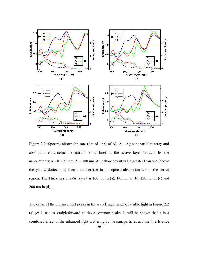
Figure 2.2: Spectral absorption rate (dotted line) of Al, Au, Ag nanoparticles array
and absorption enhancement spectrum (solid line) in the active layer
brought by the nanopatterns: a = h = 50 nm, Λ = 100 nm. An
enhancement value greater than one (above the yellow dotted line)
means an increase in the optical absorption within the active region. The
Thickness of a-Si layer t is 160 nm in (a), 140 nm in (b), 120 nm in (c)
and 200 nm in (d). . ....................................................................... 26

xi
Figure 2.3: (a) Absorption enhancement spectrum (solid line) and absorption rate
(dotted line) of Al, Au, Ag nanoparticles array: a = 30 nm, h = 50 nm, t
= 60 nm, Λ = 100 nm. (b) Absorption enhancement of Al nanopattern
with varying period Λ (a = h = 50 nm, t = 60 nm). (c) Absorption
enhancement spectrum (solid line) and absorption rate (dotted line) of Al
nanoparticles array (Λ = 100 nm, a = h = 50 nm, t = 60 nm) with 20 nm
ITO or SiO2 spacing layer. (d) A cross-sectional view of the normalized
field magnitude for the 3D structure (Λ = 100 nm, a = h = 50 nm, t = 60
nm). .............................................................................................. 30
Figure 3.1: Calculated absorption and scattering efficiencies of gold nanoparticles as
a function of wavelength of incident light and for varying particle
diameters....................................................................................... 38
Figure 3.2: Schematic diagram of the DMD-based, digital projection photo-
polymerization (DPP) system. ....................................................... 41
Figure 3.3: Schematic of the fabrication process for the log-stack microstructure.
..................................................................................................... 43
Figure 3.4: High resolution SEM images showing the surfaces of PEGDA and
MAA–PTTA micrologs on both levels. Nanoparticle-shaped features
can be observed on the surface of the MAA containing logs ((b), (d))
while they hardly exist on the other logs ((a), (c)).......................... 45
Figure 3.5: The EDS spectra taken from PEGDA and MAA–PTTA micrologs on
both levels. The difference between the two spectra is that the Au peaks
are only present in the signals from the MAA–PTTA micrologs.... 47
Figure 3.6: XPS data for the log-stack structure. The elemental Au peaks were
found in the spectrum. ................................................................... 48
xii
Figure 3.7: Picture of a Crookes radiometer. ................................................... 50
Figure 3.8: (a) Cross-sectional pattern used in the fabrication of the micro-turbine.
(b) Picture of a nanoparticle coated micro-turbine device.. ............ 51
Figure 3.9: Top view of the measurement set up.............................................. 54
Figure 3.10: (a) high-pass optical filter a, (b) band-pass optical filter b, (c) low-pass
filter c. ..................................................................................... 55-56
Figure 3.11: Absorption rate of calculated (solid curve) and measured (dots) 50 nm
Ag and Au nanoparticles on polymer material. .............................. 57
Figure 4.1: Dispersion relation of the surface plasmon polaritons along the [10]
direction of the square hole array. The momentum kx is normalized to
2π/a0. ............................................................................................ 66
Figure 4.2: (a) Three-dimensional view of the new tandem solar cell structure used
in simulation.(b) Cross-sectional view of the tandem solar cell structure.
................................................................................................ 70-71
Figure 4.3: Schematic illustration of the new tandem solar cell design ............ 73
Figure 4.4: Schematic illustration of spectrally and electrically separated
photovoltaic solar cells .................................................................. 74

xiii
Figure 4.5: (a) Optical transmission spectra T1(λ), T2(λ), and T3(λ), of the perforated
Ag electrode: t = 80 nm, W = 150 nm, Λ = 200 nm. T1 = P3/P2, T2 =
P4/P2, T3 = P4/P1. Left inset: Optical absorption enhancement in the top
polymer solar cell. Right inset: The corresponding tandem cell structure
with each interface labeled. (b) Cross-sectional view of the magnetic
field magnitude |Hy| in the solar cell model with poynting vectors
plotted together. (c) Optical transmission spectra T2(λ) for different
width W of the subwavelength holes at fixed period (Λ = 200 nm) and
film thickness (t = 50 nm). (d) Optical transmission spectra T2(λ) for
different periodicities Λ. The film thickness and the edge-to-edge
distance of any two adjacent subwavelength holes remains the same in
this case (Λ - W = 50 nm, t = 50 nm). (e) Optical transmission spectra
T2(λ) of the perforated electrode with different thickness t (W = 150 nm,
Λ = 200 nm)............................................................................. 77-79

1
Chapter 1: Introduction to Optical Phenomena of Plasmonic
Nanostructures
Any nanometer scaled structures that have plasmons related properties can be
called plasmonic nanostructures. Plasmonic nanostructures, in most cases metallic
nanostructures, exhibit many interesting and unique optical phenomena due to the
existence of surface plasmon polaritons at the metal/dielectric interface or localized
surface plasmons in the metallic nanoparticles.
1.1 DIELECTRIC FUNCTION OF FREE ELECTRON GAS
Before the detailed discussion of surface plasmon polaritons and localized surface
plasmons, the model of dielectric function of free electron gas needs to be introduced. It
plays an important role in describing the dispersion relation of the surface plasmon
polaritons and the cross section of scattering and absorption of the localized surface
plasmons.
Assume a harmonically oscillating electric field tieEE 0 is applied on a gas
of free electrons. The motion of an electron in the gas can be described by
Eetxm
txm
2
2
(1.1)
where x is the displacement of the electron, m is the mass of the electron, γ is damping
coefficient and e is the electron charge.
Solving equation 1.1 yields

2
Eim
ex
2 (1.2)
Based on the relation of macroscopic polarization of the free electron gas
xneP and the electric displacement PED 0 , the dielectric function of the free
electron gas ε(ω) can be obtained.
Eim
neED
20
2
00 1 (1.3)
iP
2
2
1 (1.4)
where n is the electron density, 0 is the electric permittivity of vacuum, m
neP
0
2
is
defined as the plasma frequency of the free electron gas. The real and the imaginary parts
of ε(ω) are
1
1Re 22
22
P (1.5)
1
1Im 22
22P (1.6)
At low frequency 1 ,
2
ImRe P , the imaginary part is
large and dominates the absolute value of ε(ω). As the frequency reaches the condition of
1 while ω is still below P ,
2
2
1)(
p (1.7)

3
As an approximation, the conduction electrons in metals can be regarded as free
electron gas. The above discussion on the dielectric function can describe the behavior of
the metals well in most of the cases.
1.2 SURFACE PLASMON POLARITONS
Surface plasmon polaritons are electromagnetic waves propagating at the
metal/dielectric interface. They are essentially oscillations of conduction electron gas on
the metal surface. Maxwell's equations state:
D (Gauss's law) (1.8)
0 B (1.9)
tBE
(Faraday's law) (1.10)
tDJH
(Ampère's law) (1.11)
where is E the electric field, H is the magnetic field, D is electric displacement, B is the
magnetic induction, J is the current density and ρ is the external charge density. For a
linear, isotropic and nonmagnetic medium,
ED 0 (1.12)
HB 0 (1.13)
EJ (1.14)

4
where ε0 and μ0 are the electric permittivity and magnetic permeability of vacuum
respectively, ε and μ are the relative permittivity and relative permeability respectively,
and σ is the conductivity.
The combination of equation 1.10 and 1.11 gives
2
2
0 tDE
(1.15)
Note that EEE 2)( and EEE )( , and assume that
0 D and 0 , equation 1.15 yields
2
2
22
tE
cE
(1.16)
a typical wave equation. Assume a plane wave propagate along x-direction on the x-y
plane (z = 0) of a Cartesian coordinate system, as shown in Figure 1.1. The electric field
can be written as )()( txki xezE . Plugging this expression into equation 1.16, we obtain
0)()( 202
2
Ekkz
zEx (1.17)
where k0 = ω/c is the wave vector in vacuum. For the magnetic field, the wave equation
has the same form as equation 1.17.

5
Figure 1.1: A plane wave propagate along x-direction on the x-y plane of a Cartesian
coordinate system.
Considering TE and TM modes separately, the wave equation can be written as
TE: 0)( 202
2
yx
y EkkzE
(1.18)
TM: 0)( 202
2
yx
y HkkzH
(1.19)
Using equation 1.10 and 1.11, the relation between E and H can be found.
For TE modes,
zEiH y
x
0
(1.20)
yx
z EkH0
(1.21)
For TM modes,

6
zHiE y
x
0
(1.22)
yx
z HkE 0
(1.23)
Given all the equations above, we can describe the surface plasmon polaritons in
the simplest case - an infinitely wide metal/vacuum interface. For convenience of
calculation, assume that the interface is at z = 0 and the metal takes z < 0 space, similar to
Figure 1.1. Considering TE wave first, equations 1.18, 1.20 and 1.21 yields,
zkxik
yAx eAezE )( (1.24)
zkxikAx
Ax eeikAzH 0
)( (1.25)
zkxikAz
Ax eekAzH 0
)( (1.26)
for z > 0, and
zkxiky
Bx eBezE )( (1.27)
zkxikBx
Bx eeikBzH0
)( (1.28)
zkxikBz
Bx eekBzH0
)( (1.29)
for z < 0, where kA and kB (both > 0) are wave vectors along the z-direction in vacuum
and metal respectively. At the surface of the metal z = 0, both Ey and Hx are continuous.
This requires A = B and A∙(kA + kB) = 0. Since both kA and kB are positive, A = B = 0. This
means TE wave does not exist on the surface.

7
For TM modes,
zkxik
yAx eAezH )( (1.30)
zkxikAx
Ax eeikAzE 0
)( (1.31)
zkxikAz
Ax eekAzE 0
)( (1.32)
as z > 0, and
zkxik
yBx eBezH )( (1.33)
zkxikBx
Bx eeikBzE 0
)( (1.34)
zkxikBz
Bx eekBzE 0
)( (1.35)
for z < 0, where ε is the dielectric constant of the metal. The continuity condition of Hy
and Ex at the metal/vacuum interface yields A = B and kB/kA = - ε. The field and the wave
of the surface plasmon polaritons is schematically illustrated in Figure 1.2. From equation
1.11 and 1.12, we know that 20
2 kkk xA and 20
2 kkk xB . Therefore, the
dispersion relation of the surface plasmon polaritons is
110
ckk x (1.36)

8
Figure 1.2: Surface plasmon polaritons wave propagating on the surface of the metal.
Assume that the dielectric constant of the metal behaves the same as that of free
electron gas discussed in section 1.1, the dispersion relation of the surface plasmon
polaritons can be obtained, as plotted in Figure 1.3.
Figure 1.3: Dispersion relation of surface plasmon polaritons on metal/vacuum interface.

9
At a low frequency ω, kx is low and follows the straight line of kx = ω/c. The wave
behaves like a photon. And 0Ak , the wave extends far toward vacuum. As the
frequency ω increases and gets closer to2P
, the dielectric constant of the metal
ε(ω) approaches to -1. As a result, kx bends over and grows to infinity. The surface
plasmon frequency is thus defined as2P
SP
. As the frequency approaches the
surface plasmon frequency, the exponential decay length of the surface plasmon polariton
along z-direction is far below the wavelength of the field. Since kx is larger than ko,
excitation of surface plasmon polaritons by a three-dimensional light beam is impossible
unless a phase-matching technique is employed on the surface.
1.3 LOCALIZED SURFACE PLASMONS
Another important excitation in plasmonics is the localized surface plasmons.
When a metal particle is placed in an alternating electromagnetic field, the oscillation of
the conduction electrons is confined within the particle if the size of the particle is
smaller than the wavelength of the field. At the resonance condition, this oscillation is
called localized surface plasmon. Unlike surface plasmon polaritons, localized surface
plasmons do not propagate and can be excited by the direct light beam without any
phase-matching techniques.
Consider a spherical particle with radius R and isotropic dielectric constant )(
in vacuum under shown in Figure 1.4. If an oscillating electric field xeEE ti 0 with

10
wavelength R2 is applied, the phase of the field across the particle can be regarded
as constant. This allows us to solve the electrostatic potential using Laplace equation
02 for the electric field both inside and outside the particle first and add the
oscillation tern e-iωt after the equation is solved. The solution of the Laplace equation is
0
)1( )(cos][),(l
ll
ll
l PrBrAr (1.37)
where Pl(cosθ) is the l order Legendre Polynomials, θ is the angle of the position vector r
and the x-axis, A and B are the constants to be determined by the boundary conditions.
Figure 1.4: Schematic illustration of an isotropic spherical particle in an electromagnetic
field.
Since the potential φ can not be infinite at r = 0, the potential inside the particle
becomes
0
1 )(cos),(l
ll
l PrAr (1.38)

11
For potential inside the particle
0
)1(2 )(cos][),(
ll
ll
ll PrBrAr (1.39)
as r → ∞, φ → -E0 z = -E0 rcosθ. This requires Al = E0 for l = 1 and Al = 0 for l ≠ 1. The
electric field can be obtained by E . At the boundary of the particle r = R, the
tangential electric field and normal displacement filed are continuous.
RrRr aa
21 11
(1.40)
RrRr rr
20
10
(1.41)
The above two equations yield the final solution of the potential inside and
outside the particle.
cos2
3),( 01 rEr
(1.42)
23
002cos
21cos),(
rRErEr
(1.43)
From equation 1.43, one can regard the subwavelength particle as a dipole. The
potential φ2 can be written as
30
02 4cos),(
rrprEr
(1.44)
where 03
0 214 ERp
is the dipole moment. Introducing the polarizability
214 3
R , the dipole moment becomes
12
00 Ep (1.45)
If the spherical particle is embedded in a homogeneous medium, the polarizability
α can simply be written asm
mR
2
4 3
, where εm is the dielectric constant of the
medium. Having obtained the solution under the electrostatic field, the oscillation term
eiωt should be added to equation 1.45. One can see that an oscillating dipole moment
tieEtp 00)( is generated by the subwavelength particle under the alternating
electric field. The electric and magnetic field produced by a dipole can be written as [1]
)(23
2
0
)(314
1)( tkriepprrcri
rrpr
rktE
(1.46)
r
eikr
prcktHtkri )(2 11
4)(
(1.47)
where r is the unit vector in any point of interest.
By calculating the Poynting vector HES , the scattering and absorption cross
sections of a spherical subwavelength particle can be obtained [2].
]Im[2
absC (1.48)
242
61
scaC (1.49)
Note that the absolute value of the polarizability reaches a maximum, which
leads to an enhancement in scattering cross section, as 2 drops to a minimum.

13
This gives the resonance condition of the particle. For a metal particle, when the
frequency 1 , 2
2
1)(
p . The resonance occurs at3p
.
Using the relation of the electric field and the potential E , the field inside
the particle can be written as
0112
3 EE
(1.50)
This is the case when the spherical subwavelength particle is placed in vacuum. If
it is embedded in a dielectric medium, equation 1.50 becomes
0112
3 EEm
m
(1.51)
Apparently, at the plasmon resonance the field inside the metal particle also gets
enhanced. It also implies that the resonance wavelength will red-shift if the dielectric
constant m increases.
1.4 APPLICATIONS OF PLASMONIC NANOSTRUCTURES
As mentioned in the last section, when the frequency of external electromagnetic
field, which is usually incident light, reaches a certain value depending on the material,
size and shape of the metal nanoparticle, localized charge oscillations will be at
resonance. One of the most straightforward phenomena at the surface plasmon resonance
frequency is the significantly enhanced near field. This property is extremely useful in
Surface Enhanced Raman Spectroscopy, often abbreviated SERS, which is an
14
enhancement of Raman scattering by molecules adsorbed on rough metal surfaces. The
enhancement factor can be as high as 1014-1015, allowing detection of single molecules
[3]. The localized surface plasmons are extremely sensitive to the surface conditions [4].
Devices exploiting this sensitivity have been widely used in the chemo- and bio-sensors
[5].
Enhanced scattering by the subwavelength metal particles both at surface plasmon
resonance and near the resonance wavelength was found extremely useful in improving
light absorption in solar cells [6, 7]. This will be elucidated in Chapter 2 in details. From
equation 1.48, one can see that the absorption cross section of a metal particle is minimal
at surface plasmons resonance, because the imaginary component of the dielectric
function is nearly zero. However, for noble metals such as silver and gold, Im is
much larger than that of free electron gas due to the interband transitions at this
frequency region (usually visible frequencies). Instead of a monotonic decrease, the
imaginary component of the dielectric function actually rises with the increasing
frequency and reaches a maximum. This implies that near the surface plasmons
resonance, the absorption of the metal subwavelength particle is also enhanced. Using
this property, researchers have demonstrated potential applications of gold/silica
core/shell nanoparticles in cancer diagnostics and therapeutics [8, 9].
Another major phenomenon observed for the plasmonic nanostructures is the
extraordinary optical transmission through metal subwavelength hole arrays. The
mechanism will be discussed in Chapter 4 in details. The most straightforward
applications are frequency selective optical filters. By varying the shape of the holes or
applying external fields, tunable transmission can be achieved in terahertz band [10-12].

15
Porto et al. demonstrated optical bistability by filling non-linear materials into sub-
wavelength apertures, which can be regarded as optical switch [13]. Wenger et al. was
able to detect single molecule fluorescence in nanoapertures [14].
This dissertation will be mainly focused on applying various plasmonic
nanostructures in energy conversion processes. Chapter 2 will continue the discussion of
the strong light scattering effect from the metal nanoparticles. It will be shown that the
light absorption in a thin film solar cell can be increased by incorporating metal
nanoparticle arrays. Based on the understanding of the absorption enhancement
mechanisms, the optimization methods for the nanostructure enhanced solar cell will be
introduced. Chapter 3 emphasizes the accompanying high optical absorption within the
metal nanoparticles near the surface plasmon resonance frequency. As a frequency
sensitive heat generator, metal nanoparticles can give the function of wavelength
selectivity to a light-driven micro-turbine device. In order to demonstrate wavelength
controlling of a nanoparticle coated micro-turbine, a technique that can selectively
localize metal nanoparticles in a three-dimensional fashion was developed. In Chapter 4,
a fascinating phenomena – extraordinary optical transmission through metal film
perforated with subwavelength hole arrays will be described. A novel tandem solar cell
structure that has the perforated metal film placed between the top and the bottom sub-
cells as an intermediate common electrode will be revealed in details. It will be seen that
the new design has many advantages over the conventional tandem cell structure and is
generally applicable to different types of tandem solar cell. The last chapter gives a
summary of the whole research and an outlook towards the future study.
16
Reference
1. Jackson, J.D. Classical Electrodynamics, 3rd edition, (John Wiley & Sons, New
York 1999).
2. Bohren, C. F. and Huffman, D. R., Absorption and Scattering of Light by Small
Particles, (Wiley-Interscience, New York, 1983).
3. Nie, S. and Emory, S. R., "Probing Single Molecules and Single Nanoparticles by
Surface-Enhanced Raman Scattering," Science, 275, 1102 (1997).
4. Zayats, A. V.; Smolyaninov, I. I. and Maradudin, A. A. "Nano-optics of surface
plasmon polaritons," Physics Reports-Review Section of Physics Letters, 408, 131
(2005).
5. Boisdé, G. and Harmer, A. Chemical and biochemical sensing with optical fibers
and waveguides, The Artech House optoelectronics library (Artech House,
Boston, 1996).
6. Wu, S.; Wang, W.; Reinhardt, K.; Lu, Y. and Chen, S. C. "Absorption
Enhancement in Thin Film Si Solar Cells by Two Dimensional Periodic
Nanopatterns," Journal of Nanophotonics, accepted to publish.
7. Akimov, Y. A. and Koh, W. S. "Resonant and nonresonant plasmonic
nanoparticle enhancement for thin-film silicon solar cells," Nanotechnology, 21,
235201 (2010).
8. Choi, M.-R.; Stanton-Maxey, K. J.; Stanley, J. K.; Levin, C. S.; Bardhan, R.;
Akin, D.; Badve, S.; Sturgis, J.; Robinson, J. P.; Bashir, R.; Halas, N. J. and
Clare, S. E. "A Cellular Trojan Horse for Delivery of Therapeutic Nanoparticles
into Tumors," Nano Letters, 7 (12), 3759 (2007).

17
9. Fortina, P.; Kricka, L. J.; Graves, D. J.; Park, J.; Hyslop, T.; Tam, F.; Halas, N. J.;
Surrey, S. and Waldman, S. A. "Applications of nanoparticles to diagnostics and
therapeutics in colorectal cancer," Trends in Biotechnology, 24 (4), 145 (2007).
10. Battula, A. and Chen, S. C. "Extraordinary Transmission in a Narrow Energy
Band for Metallic Nano-gratings with Converging-Diverging Channels", Appl.
Phys. Lett., 89 (13), 131113 (2006).
11. Battula, A.; Chen, S. C.; Lu, Y.; Knize, R. J. and Reinhardt, K. "Tuning the
extraordinary optical transmission through subwavelength hole array by applying
a magnetic field", Optics Letters, 32 (18), 2692 (2007).
12. Battula, A.; Lu, Y.; Knize, R. J.; Reinhardt, K. and Chen, S. C. "Tunable
extraordinary optical transmission at 100 THz through a metallic hole array with a
varying hole shape", Opt. Express, 15 (22), 14629 (2007).
13. Porto, J. A.; Martin-Moreno, L. and Garcia-Vidal, F. J. "Optical bistability in
subwavelength slit apertures containing nonlinear media," Phys. Rev. B, 70,
081402 (2004).
14. Wenger, J.; Lenne, P.-F.; Popov, E.; Rigneault, H.; Dintinger, J. and Ebbesen T.
"Single molecule fluorescence in rectangular nano-apertures," Opt. Express, 13
(18), 7035 (2005).

18
Chapter 2: Enhanced Optical Scattering by Metal Nanoparticles and
its Application in Solar Cells Absorption Improvement
2.1 ABSTRACT
Metallic nanostructures such as nanoparticles and nanowires exhibit extraordinary
optical properties in absorption, scattering and transmission of electromagnetic radiation
due to the excitation of collective oscillations of the conduction electrons on the surface
of nanostructures, called surface plasmons. This allows them to provide applications in
converting photon energy to other forms of energy in a more efficient manner.
A major problem of current silicon thin film solar cells lies in low carrier
collection efficiency due to short carrier diffusion length. Instead of improving the
collection efficiency in a relatively thick solar cell, increasing light absorption while still
keeping the active layer thin is an alternative solution. When incorporated into an
amorphous silicon thin film solar cell, nanoparticles were found to substantially increase
the light absorption in the photoactive layer within certain wavelength range. The
mechanism of this optical absorption was studied using three-dimensional finite element
method. It was found that intensified Fabry-Perot resonance in the active layer due to the
addition of the nanostructures and enhanced light scattering by the plasmonic
nanostructures were both responsible for this phenomenon. Interestingly, higher
absorption only occurs at wavelength range outside the surface plasmons resonance of the
nanostructures. A further study on the absorption of the nanoparticles themselves
revealed that enhanced near field associated with the SP resonance of particles causes
extraordinary energy dissipation in the particles, resulting in decreased light coupling into
the active layer.

19
2.2 INTRODUCTION TO SURFACE PLASMON ENHANCED LIGHT SCATTERING
As mentioned in Chapter 1, metal nanoparticles exhibit unique optical properties
due to the excitation of the localized surface plasmons by the incident light. At
wavelength near the surface plasmon resonance, the incident light is strongly scattered or
absorbed. A point dipole is a perfect approximation to describe this optical phenomenon
for a particle with its size far below the wavelength of the incident light. The scattering
and absorption cross sections can be written as [1]:
]Im[2
absC (2.1a)
242
61
scaC (2.1b)
where α is the polarizability of the particle, given by α =
m
mV2
3 , V is the volume
of the particle, and m are the dielectric constants of the metal nanoparticle and the
surrounding dielectric media respectively. The scattering efficiency Qsca is given by Qsca
= Csca/(Csca+ Cabs). At the surface plasmon resonance frequency, the permittivity of the
metal and dielectric materials exactly satisfies = -2 m . This leads to an infinite
scattering cross-sectional area, much larger than the geometric cross-sectional area of the
particle. Factors that affect the surface plasmon resonance frequency include particle
material, size, shape, and refractive index of the surrounding medium [2]. For example,
the resonance wavelength of a silver nanoparticle is shorter than that of a gold
nanoparticle with the same size and shape. Alloying the two metals in the different ratios
can tune the resonance between the resonance wavelength of the pure gold and silver
20
particles [3]. Moreover, shrinking the size of the metal nanoparticle can cause a blue-shift
of resonance wavelength while increasing the dielectric constant of the surrounding
medium leads to a red-shift of the resonance frequency [4]. Because of the enhanced
scattering and the tunability of the surface plasmons, quite a few optical or optoelectronic
devices can be beneficial by the incorporation of metal nanoparticles. Silicon thin film
solar cells are one of them.
Silicon thin film solar cells catch extensive research interests due to the
significant cost advantage over their bulk crystalline predecessors, Yet, before they can
become a competitive candidate as a major solar energy source, efficiency still needs to
be increased. The main challenge for improving the efficiency lies in the fact that the
material used in the active region of a thin film solar cell is usually either polycrystalline
or amorphous. The carrier life time (τ) in such materials is quite low. This results in a
short diffusion length. Therefore, expectation of both efficient carrier collection and low
cost production will prefer the use of a thin layer of light absorbing material. On the other
hand, the light absorbing material has to be thick enough to ensure maximum carrier
generation. Instead of improving the charge collection efficiency using a relatively thick
solar cell, increasing the light absorption while still keeping the active layer thin will be
an alternative way to resolve this dilemma. The most common method previously used
for absorption enhancement is by introducing scattering surface textures [5] for light
trapping. However, this is not a viable option for thin film solar cells because the
roughness of these surface textures is of the same order as the thickness of the thin-film
active layer. Increased surface recombination resulting from an enlarged surface area will
deteriorate the overall cell performance.

21
Recently, ideas of employing nanoscale metallic materials to improve the light
absorption of solar cells have been gaining attention. Early work, such as the
incorporation of small copper or silver clusters in an organic solar cell to increase the
photovoltaic conversion efficiency, was done by Stenzel and Westphalen [6-7] in the late
1990s. An increase in the short circuit current by a factor of 2 was reported. In the past
few years, gold or silver nanoparticles with sizes ranging from tens of nanometers to over
a hundred nanometers were introduced to both crystalline [8-9] and amorphous [10]
silicon solar cells. Enhancement in both photocurrent and conversion efficiency were
experimentally observed. All of such performance improvements were attributed to light
scattering by surface plasmons (SP). However, a latest study by Pala has shown that the
previous observation may not be only from the SP effect [11]. Because that current
computer technology has made simulation of electromagnetic (EM) field on many
sophisticated nanoscale structures possible, various plasmonic nanostructures have been
proposed, and their potential in improving solar cell performance has been investigated
[12-15]. Most of such work, however, were numerical analyses on two-dimensional
structures and considered only one polarization of an incident light. This not only restricts
their designs to one-dimensional plasmonic structures such as nanowires or nanogratings,
but is also insensitive to the randomly polarized nature of solar radiation.
To establish a more realistic analysis, in the following section, the discussion is
focused on a three-dimensional (3D) thin film plasmonic solar cell model with a periodic
metal nanoparticle array incorporated. The periodic pattern not only facilitates the setting
of boundary conditions in simulation, but also allows an in-depth investigation of
absorption enhancement effects from a single nanoparticle and multiple particles
22
simultaneously. By simulating the EM field in a chosen model structure using 3D finite
element method, effects from incorporating various nanopatterns can be studied. These
results were used to identify different enhancement mechanisms and derive the criteria
for optimizing a nanostructure-enhanced thin film solar cell.
2.3 ABSORPTION ENHANCEMENT IN SILICON THIN FILM SOLAR CELLS BY TWO-DIMENSIONAL PERIODIC NANOPARTICLE ARRAYS
2.3.1 Computational Details
Figure 2.1 shows a typical Si thin film solar cell structure with a periodic
nanopattern on top. This structure was simulated in COMSOL Multiphysics, a
commercial 3D finite element analysis software. In this model, amorphous Si (a-Si) was
chosen as the active material. Compared to polycrystalline Si, a-Si has a larger absorption
rate, and thus is more suitable to be used as a light absorbing material in a nanoscale
device. An Al film with thickness fixed at 100 nm was placed underneath the active layer
as the bottom electrode. In a real a-Si solar cell, the bottom electrode is usually much
thicker and might be other metal materials. Having tried materials, such as Au, Ag, Ti,
and other thickness values that are larger than 100 nm for the bottom electrode, we
observed no difference on the optical performance of the solar cell within the wavelength
range of interests. Either as a top contact or as a passivation layer, a dielectric spacing
layer was introduced between the nanoparticle array and the a-Si film. The incident solar
radiation was assumed to be along z-axis. Since solar radiation is equally distributed in
either one of the two polarizations, the dimension, geometry, and optical properties of the
nanopattern were set to be identical in both x and y, so that only one polarization of the
23
incident light needs to be considered for this study. By setting periodic boundary
conditions on four faces surrounding each repeating unit in the x and y dimensions, the
whole structure can be simplified into one unit. Perfectly matched layers (PML) were
used to eliminate unnecessary reflection at the top and bottom boundaries of the
simulated domain. The dielectric constant data were taken from Ref. 16 and 17.
Based on the Poynting theorem, the time-averaged absorption in the active
material is
dVEAbsorptionV
2
21 (2.2)
where E is the steady-state electric field, V is the volume of the active layer and the
)Im( is the product of the frequency of the oscillating electric field and the
imaginary part of the dielectric constant. To calculate the absorption enhancement )(
at different wavelengths,
)()()(
cellsolarreferenceAbsorptionnnanopatterwithcellsolarAbsorption
(2.3)
a reference solar cell with the same structure except the nanopattern on top was
introduced. An enhancement value greater than one means absorption in the active layer
is increased due to the presence of the nanostructure. Considering the energy distribution
spectrum of solar energy and the spectral response of the solar cell, the wavelength range
of interest was chosen to be from the ultraviolet to near infrared. The following
components were varied to identify possible enhancement mechanisms: the lateral
dimension a and the vertical dimension h of each nanoparticle, the period Λ, the material

24
and dielectric environment of the nanoparticle array, and thickness t of the photoactive
material.
Figure 2.1: Structure of the nanopattern incorporated solar cell model to be used in
simulation.
2.3.2 Absorption Enhancement Mechanisms
The nanopattern-induced absorption enhancement with respect to the wavelength
of the incident light in a particular solar cell structure is shown in Figure 2.2 (a). In this
model, the a-Si layer thickness was chosen to be 160 nm. The reasons to select this
thickness are not only to consider the optical absorption rate of a-Si material in order to
leave enough room for enhancement, but also to allow for a possible observation of
different enhancement mechanisms. The nanopattern has a period of 100 nm and each
nanoparticle is 50 nm in all three dimensions. This array is placed on top of the active

25
region with a 20 nm thick Indium Tin Oxide (ITO) in between as a contact layer.
Nanoparticle arrays of three different materials, Ag, Al and Au, were studied. All of the
three enhancement curves show two common features, a peak and a valley centered at
about 990 nm and 870 nm respectively. This is attributed to the Fabry-Perot cavity
resonance within the a-Si film with the peak and the valley corresponding to the
constructive and the destructive interference respectively. As the thickness of a-Si layer
was reduced to 140 nm (Figure 2.2 (b)) and 120 nm (Figure 2.2 (c)), such common peaks
and valleys blue-shifted. It is understandable according to the changed cavity length.
26
Figure 2.2: Spectral absorption rate (dotted line) of Al, Au, Ag nanoparticles array and
absorption enhancement spectrum (solid line) in the active layer brought by the
nanopatterns: a = h = 50 nm, Λ = 100 nm. An enhancement value greater than one (above
the yellow dotted line) means an increase in the optical absorption within the active
region. The Thickness of a-Si layer t is 160 nm in (a), 140 nm in (b), 120 nm in (c) and
200 nm in (d).
The cause of the enhancement peaks in the wavelength range of visible light in Figure 2.2
(a)-(c) is not as straightforward as those common peaks. It will be shown that it is a
combined effect of the enhanced light scattering by the nanoparticles and the interference
27
of the scattered light inside the a-Si Fabry-Perot cavity. Metallic nanostructures are
known to be capable of scattering light with a scattering cross-section larger than their
own size through excitation of SP [1]. At the same time, enhanced near field associated
with the SP resonance also causes extraordinary optical absorption by the nanostructures
themselves. This fact is confirmed by the spectral absorption rate of the nanopattern, also
shown in Fig. 2(a)-(c). Strong optical absorption by the nanopattern of each material
always emerges in the vicinity of its SP resonance wavelength. As a result, a considerable
portion of the incident power is dissipated in the nanoparticles before scattered into the
photoactive material underneath. This explains why the absorption enhancement in the
active layers is always less than one at the wavelength range where strong absorption in
the nanostructure occurs. For Ag and Au nanopatterns, since their SP resonance lies in
the visible light region, the enhancement bandwidth appears to be narrow. In contrast, Al
particles have a much wider enhancement range, because their resonant wavelength is in
the ultraviolet region. Similar results were also reported by other researcher recently [18].
An important feature in the relatively wide enhancement band of the Al nanopattern
shown in Figure 2.2 (a) is the valley at 600 nm. The mechanism behind is the destructive
interference of nanostructure scattered light inside the thin a-Si cavity. It is the
superposition of the destructive minimum on the enhancement band of the Al
nanoparticles in the visible region that splits the enhancement band into two peaks. As
can been seen in Figure 2.2 (b) and (c), the destructive minimum blue-shifts and
eventually moves out of the Al enhancement band, with the decreasing thickness of the a-
Si layer. Same phenomena were not observed for the Ag and Au nanopattern in the same
region, since their enhancement bandwidth is relatively narrow. However, the
28
suppression of their enhancement peaks by the destructive interference can still be clearly
observed in Figure 2.2 (b) and (c).
2.3.3 Optimization Criteria for the Plasmonic Solar Cell Design
Based on the discussion above, one way to expand the bandwidth of the
enhancement is to push the common valley at 870 nm in Figure 2.2 (a) to even longer
wavelengths. This can be achieved by increasing the thickness of the a-Si layer. Shown in
Figure 2.2 (d), as the active layer becomes 200nm thick, the bandwidth of three
enhancement curves all substantially increased. However, since the absorption of a-Si
vanishes beyond 800 nm and most of the solar energy lies in the visible band, extending
the enhancement band towards infrared does little contribution to the efficiency of the
solar cells. The key is to extend the enhancement band towards shorter wavelength,
especially for Ag and Au nanoparticles. Shrinking the size of the nanoparticles to blue-
shift the SP resonance is a reasonable thought. Figure 2.3 (a) shows the enhancement and
absorption spectra of the three nanopatterns when the lateral dimension of each
nanoparticle decreases from 50 nm to 30 nm. To minimize the influence of the
destructive interference to the absorption enhancement in the active layer, we set the
thickness of the a-Si film to be 60nm only. Not surprisingly, the SP resonance
wavelengths all blue-shift. Consequently, the enhancement band of all three materials
expands towards the shorter wavelength. Although the density of the nanoparticles
remained unchanged as we cut the lateral dimension of the nanoparticles, the coverage
which is the percentage of the area covered by the metallic nanoparticles was reduced.
Compared with the 50 nm wide nanoparticels in Fig. 2, the lower coverage of the 30 nm

29
nanoparticles directly gives rise to the significant drop of the enhancement intensity in
Figure 2.3 (a). Shown in Figure 2.3 (b), for the nanoparticles with the same sizes, when
they are placed far apart, there is hardly any interaction of the SPs between adjacent
particles. Changing the coverage only affects the enhancement intensity, but not the
enhancement wavelength range. As the edge-to-edge distance of the nanoparticles falls
below 25 nm, multiple-scattering effect of SPs becomes noticeable [19], resulting in a
red-shift of the SP resonance wavelength and a correspondingly narrowed enhancement
bandwidth.
The SP resonance wavelength of a nanoscale object is also highly sensitive to its
dielectric environment. As shown in Figure 2.3 (c), replacing the ITO spacing layer by
SiO2 (a material with smaller dielectric constant), a substantial blue-shift of the SP peak
can be observed in the absorption rate curve. Given the large enhancement wavelength
tuning range, considerations on the dielectric layer placed between the nanopattern and
the active material is also important in designing the nanostructure-enhanced solar cells.
Figure 2.3 (d) shows a cross-sectional view of steady-state magnetic field distribution in a
60 nm thick a-Si film with 50 nm wide Al nanoparticle array on top. The simulated field
is the y-direction magnetic field Hy with a wavelength of 590 nm. The intensity of the
field is normalized to the incident radiation. Although not at the resonance wavelength,
strong charge oscillation in x-direction are still excited by the incident light with the
electric field polarized in x-direction. This can be evidenced by the intense y-direction
magnetic field Hy concentrated at the interface of the nanoparticle and the ITO layer. The
stripes inside the a-Si layer are an indication of Fabry-Perot interference within the a-Si
cavity.
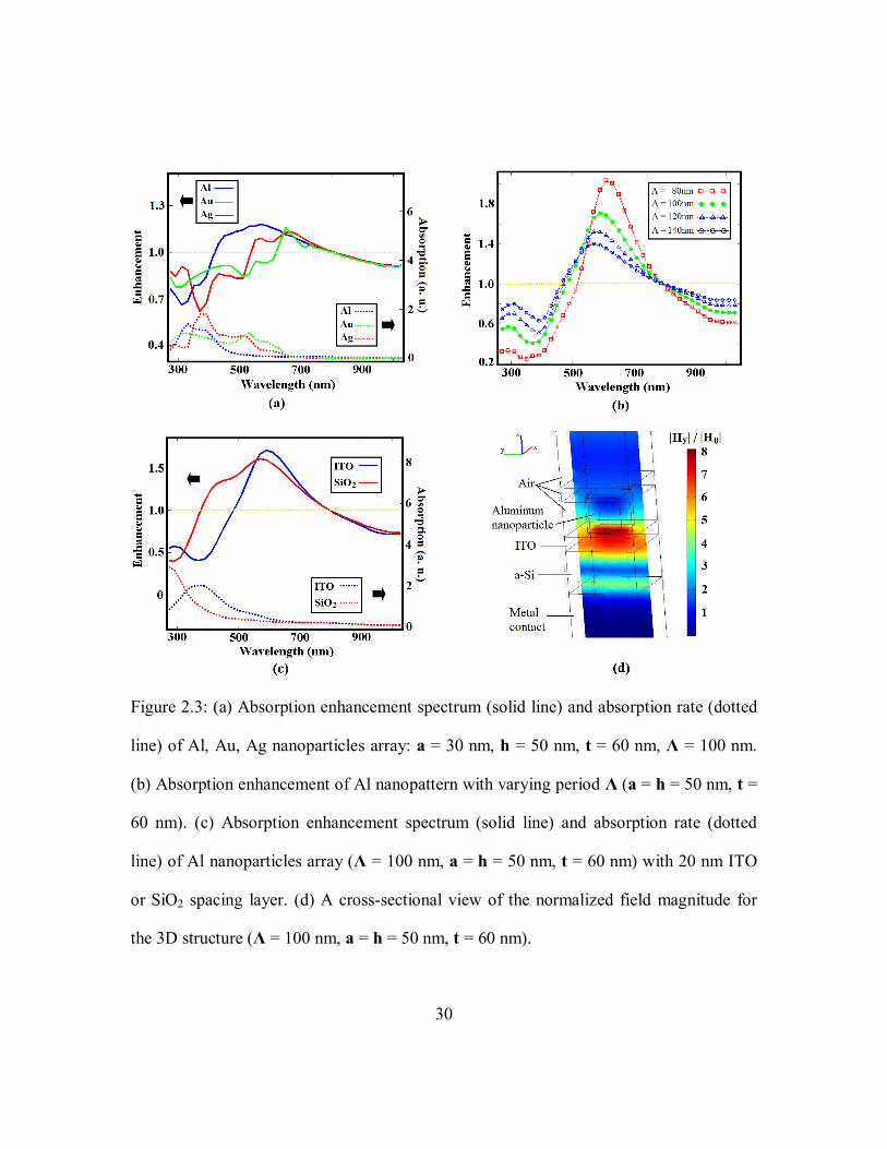
30
Figure 2.3: (a) Absorption enhancement spectrum (solid line) and absorption rate (dotted
line) of Al, Au, Ag nanoparticles array: a = 30 nm, h = 50 nm, t = 60 nm, Λ = 100 nm.
(b) Absorption enhancement of Al nanopattern with varying period Λ (a = h = 50 nm, t =
60 nm). (c) Absorption enhancement spectrum (solid line) and absorption rate (dotted
line) of Al nanoparticles array (Λ = 100 nm, a = h = 50 nm, t = 60 nm) with 20 nm ITO
or SiO2 spacing layer. (d) A cross-sectional view of the normalized field magnitude for
the 3D structure (Λ = 100 nm, a = h = 50 nm, t = 60 nm).

31
2.3.4 Calculation of Overall Enhancement in Solar Cells
As to a real solar cell, it is more important to evaluate the electrical output
performance. For an a-Si solar cell that is thin enough to assume 100% charge collection
efficiency, the increase in short-circuit current can be calculated as
dIA
dIA
0
0
)()(
)()()( (2.4)
where κ(λ) is the absorption enhancement obtain from the simulation of a specific
nanopatten enhanced solar cell structure, A(λ) is the absorption rate of the active layer for
the reference solar cell without any nanoparticles, and I(λ) is the incident photon flux
converted from the AM1.5G solar radiation spectrum. If the device has less than ideal
carrier collection efficiency, the quantum efficiency η(λ) needs to be considered. The
photocurrent enhancement becomes
dIA
dIA
0
0
)()()(
)()()()( (2.5)
The quantum efficiency data can be taken from Ref. 20. The quantum efficiency
may change depending on specific device structures, however, the resulting α will not
change as long as the shape of the η(λ) vs. λ curve remains the same. The Al nanoparticle
array corresponding to the blue curve in Figure 2.2 (d) can easily give a 20%
enhancement in photocurrent.

32
2.4 SUMMARY
Absorption enhancement in a thin film Si solar cell by incorporating a two
dimensional metallic nanoparticle array was studied using 3D finite element analysis. We
have identified two different enhancement mechanisms and considered the influences of
the active layer thickness and the material, dimension, coverage, and dielectric
environment of the metallic nanopattern in order to demonstrate a way to optimize the
nanostructure for maximum solar cell performance improvement. Suffering from the high
energy dissipation in the visible range, the Ag and Au nanopatterns did not provide good
absorption enhancement to the solar cells. On the other hand, Al nanoparticles array
brought considerable increase in absorption although they were not in SP resonance at the
wavelength of highest enhancement. By considering photon distribution of the solar
radiation, the quantum efficiency and the absorption rate of active material, a 20%
increase of the photocurrent can be easily achieved. Using the same designing method,
the nanopattern can also be applied to other thin film solar cells with different light
absorbing materials such as Copper indium gallium selenide (CIGS), CdTe and even
organic films.
Reference
1. Bohren, C. F. and Huffman, D. R., Absorption and Scattering of Light by Small
Particles, (Wiley-Interscience, New York, 1983).

33
2. Kreibig, U. and Vollmer, M. Optical Properties of Metal Cluster, (Wiley, New
York, 1995).
3. Baba, K.; Okuno, T. and Miyagi, M. "Silver–gold compound metal island films
prepared by using a two-step evaporation method," Appl. Phys. Lett., 62, 437
(1993).
4. Xu, G.; Tazawa, M.; Jin, P.; Nakao, S. and Yoshimura, K. "Wavelength tuning of
surface plasmon resonance using dielectric layers on silver island films," Appl.
Phys. Lett., 82, 3811 (2003).
5. Green, M. A. "Lambertian light trapping in textured solar cells and light-emitting
diodes: analytical solutions," Progress in Photovoltaics: Research and
Applications, 10, 235 (2002).
6. Westphalen, M.; Kreibig, U.; Rostalski, J.; Lüth, H. and Meissner, D. "Metal
cluster enhanced organic solar cells," Sol. Energy Mater. Sol. Cells, 61, 97 (2000).
7. Stenzel, O.; Stendal, A.; Voigtsberger, K. and Borczykowski, C. V.
"Enhancement of the photovoltaic conversion efficiency of copper phthalocyanine
thin film devices by incorporation of metal clusters," Sol. Energy Mater. Sol.
Cells, 37, 337 (1995).
8. Pillai, S.; Catchpole, K. R.; Trupke,T. and Green, M. A. "Surface plasmon
enhanced silicon solar cells," J. Appl. Phys., 101, 093105 (2007).
9. Schaadt, D. M.; Feng, B. and Yu, E. T. "Enhanced semiconductor optical
absorption via surface plasmon excitation in metal nanoparticles," Appl. Phys.
Lett., 86, 063106 (2005).
10. Derkacs, D.; Lim, S. H.; Matheu, P.; Mar, W. and Yu, E. T. "Improved
performance of amorphous silicon solar cells via scattering from surface plasmons
polaritons in nearby metallic nanoparticles," Appl. Phys. Lett., 89, 093103 (2006).

34
11. Pala, R. A.; White, J.; Barnard, E.; Liu, J. and Brongersma, M. L. "Design of
Plasmonic Thin-Film Solar Cells with Broadband Absorption Enhancements,"
Adv. Mater., 21, 1 (2009).
12. Catchpole, K. R. and Polman, A. "Design principles for particle plasmon
enhanced solar cells," Appl. Phys. Lett., 93, 191113 (2008).
13. Rockstuhl, C.; Fahr, S. and Lederer, F. "Absorption enhancement in solar cells by
localized plasmon polaritons," J. Appl. Phys., 104, 123102 (2008).
14. Ferry, V. E.; Sweatlock, L. A.; Pacifici, D. and Atwater, H. A. "Plasmonic
Nanostructure Design for Efficient Light Coupling into Solar Cells," Nano Lett., 8
(12), 4391 (2008).
15. Wang, W.; Wu, S.; Reinhardt, K.; Lu, Y. and Chen, S. C. "Broadband Light
Absorption Enhancement in Thin-Film Silicon Solar Cells," Nano Lett., 10 (6),
2012 (2010).
16. Palik, E. D. Handbook of Optical Constants of Solids, 1, 290, (Academic, San
Diego, CA 1985).
17. Mergel D. and Qiao, Z. "Correlation of lattice distortion with optical and
electrical properties of In2O3:Sn films," J. Phys. D, 35, 794 (2002).
18. Akimov, Y. A. and Koh, W. S. "Resonant and nonresonant plasmonic
nanoparticle enhancement for thin-film silicon solar cells," Nanotechnology, 21,
235201 (2010).
19. Han, L.-H.; Wang, W.; Lu, Y.; Knize, R. J.; Reinhardt, K.; Howell, J. R. and
Chen, S. C. "Analytical and Experimental Investigation of Electromagnetic Field
Enhancement among Nanospheres with Varying Spacing," Journal of Heat
Transfer, 131, 033110 (2009).

35
20. Meier, J.; Spitznagel, J.; Kroll, U.; Bucher, C.; Fay, S.; Moriarty, T. and Shah, A.
"High-efficiency amorphous and ‘micromorph’ silicon solar cells," Proceedings
of the 3rd World Conference on PVSEC, Osaka, Japan, 3, 2801 (2003).
36
Chapter 3: Surface Plasmon Induced Absorption and Wavelength
Sensitive Light-Driven Micro-turbine
3.1 ABSTRACT
Strong power dissipation accompanied with the surface plasmons resonance
becomes desirable when nanostructures are used as a heat generator. Using the new
technique of three-dimensional localization of the metallic nanoparticles on polymer
microstructures, wavelength dependent controlling of a light-driven micro-turbine was
achieved by selectively coating it with nanoparticles of different materials.
The new technique of three-dimensional seletive growth of the metallic
nanoparticles integrates 3D direct writing of heterogeneous microstructures with
nanoparticle synthesis. A digital micromirror device is employed as a dynamic mask in
the digital projection photopolymerization (DPP) process to build the heterogeneous
microstructure layer by layer. An amine-bearing polyelectrolyte, branched
poly(ethylenimine), is selectively attached to the microstructure and acts as both a
reducing and a protective agent in the nanoparticle synthesis. Scanning electron
microscopy, energy dispersive x-ray spectroscopy and x-ray photoelectron spectroscopy
are utilized to characterize the microstructure and confirm the 3D selectivity of the
nanoparticle growth.
The new technique allows for coating different metallic nanoparticles to a
polymeric micro-turbine fabricated by the DPP process. Placed in a partial vacuum
environment, the micro-turbine is driven by the convection due to the temperature
gradient across each vane when being illuminated under light. The heat generation rate of

37
the nanoparticles varies at different wavelength depending on the size, shape and material
of the particles. By coating Ag and Au nanoparticles on two identical micro-turbines
respectively, wavelength controlling of the micro-turbine was demonstrated.
3.2 INTRODUCTION TO SURFACE PLASMONS INDUCED ABSORPTION
As mentioned in Chapter 2, when calculating the optical absorption of a
nanoparticle, the absorption cross section Cabs or absorption efficiency Qabs (Cabs
/geometric cross-sectional area) are always referred.
As an example, the absorption and scattering efficiency Qabs of a gold particle can
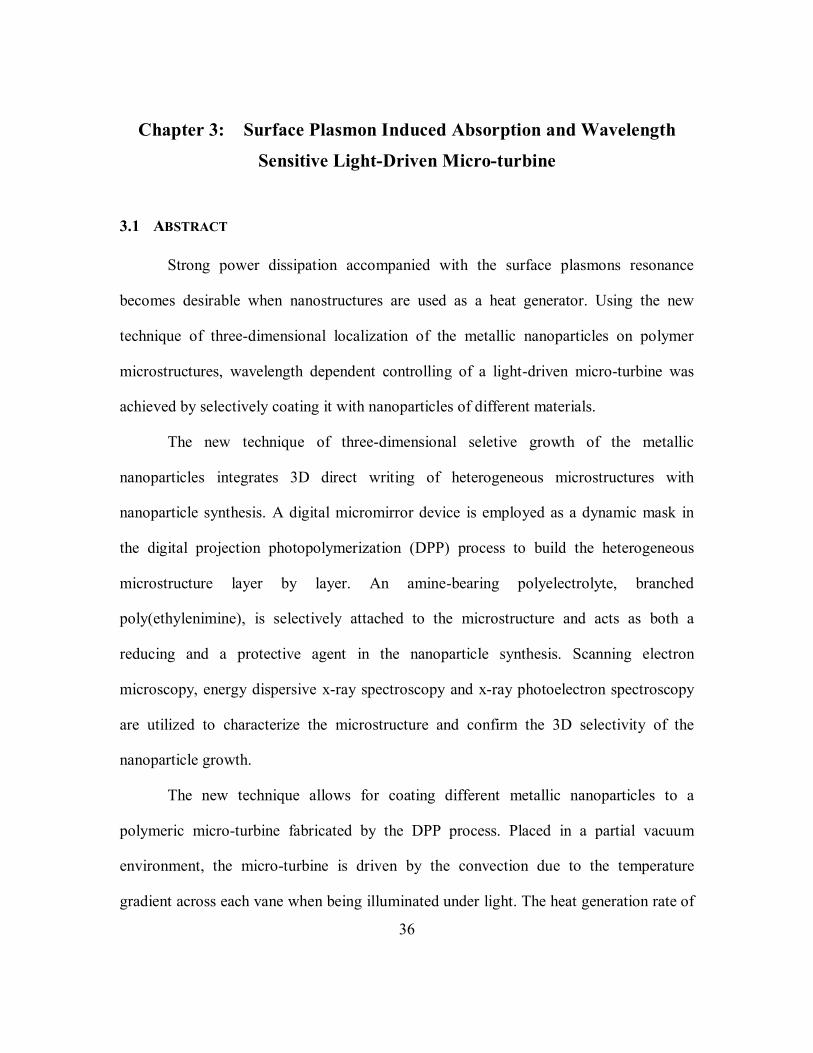
be calculated based on Mie Theory [1], shown in Figure 3.1 [2]. One can see that for gold
particles with diameters less than 120 nm, the absorption efficiency reaches a maximum
at certain wavelength. The overall absorption efficiency increases with the size of the
particle until it reach a peak value at a diameter of ~60nm and then decreases as the
particle size continues to expand. Comparing it with the scattering efficiency spectrum,
one can conclude that smaller particles tend to absorb more light than scattering it. The
absorption cross section can also be determined experimentally using a spatial
modulation technique [3]. It has been show that the measurement results fit well with the
calculated date [4].
38
Figure 3.1: Calculated absorption and scattering efficiencies of gold nanoparticles as a
function of wavelength of incident light and for varying particle diameters [2].
Absorbed light by the metal nanoparticles generates considerable heat and is
subsequently released into the ambient environment of the particle by conduction and
radiation. Unlike the scattering efficiency, the absorption efficiency changes more rapidly
at the wavelength range where the peak value is located. Applications such as solar
glazing, nanoscale lithography, and therapeutic applications [2, 5] have been reported.
In the next two sections, a new technique that can localize metallic nanoparticles
three-dimensionally in a polymer structure will be described. It will also be shown that
wavelength dependent control can be achieved in a light-driven micro-turbine by
attaching different nanoparticles onto the polymeric device.

39
3.3 THREE-DIMENSIONAL SELECTIVE GROWTH OF NANOPARTICLES ON A
POLYMER MICROSTRUCTURE
3.3.1 Background Introduction
Nanomaterials and nanostructures have drawn much attention due to their unique
electronic, optical and chemical properties. To date, significant efforts have been devoted
to the synthesis of various nanostructures such as nanowires, nanotubes, nanoshells and
nanotripods [6–9]. These nanostructures have an assortment of compositions and
properties, and range from elemental to compound materials and from conductors to
insulators. Despite the successes in controlling the size, shape, composition distribution
and state of nanomaterials, technologies for the spatial manipulation, ordered distribution
or selective localization are still lacking. These problems present a major hurdle to be
overcome before the proven potential of nanostructures can be applied in real
applications.
Significant work includes the development of optical tweezers that can
manipulate nanometer-sized dielectric particles in three dimensions, by Ashkin et al and
Chu [10, 11]. However, optical tweezers are limited as regards the number of
nanoparticles that can be controlled for both motion and position at the same time.
Different methods of aligning nanowires and nanotubes on substrates have also been
demonstrated [12–14], but the ordering is only in two dimensions.
To realize three-dimensional (3D), active, heterogeneous microsystems, it is
imperative to control the nanostructures in the microdevice selectively in a 3D fashion.
Current microfabrication and nanofabrication techniques such as photolithography and
nanoimprinting are 2D in nature. Little work has been done on extending two-

40
dimensional patterning to three dimensions. The capability of 3D localization of
nanostructures will not only provide more functionalized area in a device, but also allow
numerous 3D applications to be explored.
In this work, we will demonstrate the selective growth of Au nanoparticles in a
patterned 3D polymer microstructure. Using a multi-material digital projection
photopolymerization (DPP) technique [15], we fabricate a heterogeneous polymer
microstructure layer by layer. We then grow Au nanoparticles in selected areas of the
polymer microstructure. Materials characterization is carried out to confirm the selective
decoration of the Au nanoparticles on the 3D microstructure.
3.3.2 Digital Photopolymerization
As illustrated in Figure 3.2, the DPP fabrication system includes a digital
micromirror device (DMD) chip, a UV light source, a projection lens set, a height
adjustable sample stage and a monomer container with feeding/purging outlets capped
with a flat glass substrate. A 3D microstructure model created by computer-aided design
(CAD) software was split into a sequence of cross-sectional images. These images were
then reassembled by digitally forming a reflecting pattern on the micromirror array in the
DMD chip. A homogenized UV light beam reaching the micromirror array was reflected
and projected onto the image plane located between the glass substrate and the sample
stage. Upon exposure to the UV light, the photo-curable liquid monomers at the image
plane were polymerized and solidified, translating the cross-sectional image into a layer
of the microstructure to be fabricated. If another part of the previously formed layer is to
be built with a different polymer material, the liquid in the container can be switched to

41
other kinds of monomers through the feeding/purging outlets and photopolymerized
according to another corresponding pattern on the micromirror array. Once one layer of
the microstructure was completed, the sample stage was lowered by an amount that is
exactly equal to the thickness of the next layer to be cured. The process was repeated to
stack one layer onto another until the desired 3D heterogeneous microstructure was
finished.
Figure 3.2: Schematic diagram of the DMD-based, digital projection photo-
polymerization (DPP) system.
42
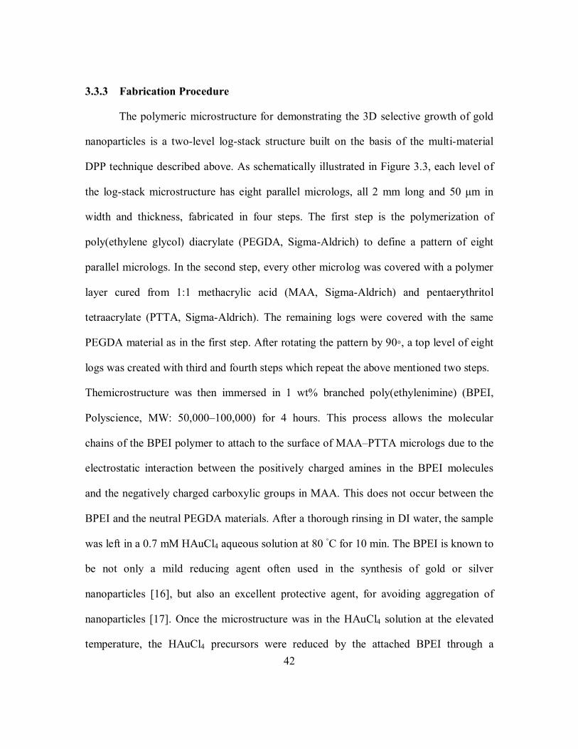
3.3.3 Fabrication Procedure
The polymeric microstructure for demonstrating the 3D selective growth of gold
nanoparticles is a two-level log-stack structure built on the basis of the multi-material
DPP technique described above. As schematically illustrated in Figure 3.3, each level of
the log-stack microstructure has eight parallel micrologs, all 2 mm long and 50 μm in
width and thickness, fabricated in four steps. The first step is the polymerization of
poly(ethylene glycol) diacrylate (PEGDA, Sigma-Aldrich) to define a pattern of eight
parallel micrologs. In the second step, every other microlog was covered with a polymer
layer cured from 1:1 methacrylic acid (MAA, Sigma-Aldrich) and pentaerythritol
tetraacrylate (PTTA, Sigma-Aldrich). The remaining logs were covered with the same
PEGDA material as in the first step. After rotating the pattern by 90◦, a top level of eight
logs was created with third and fourth steps which repeat the above mentioned two steps.
Themicrostructure was then immersed in 1 wt% branched poly(ethylenimine) (BPEI,
Polyscience, MW: 50,000–100,000) for 4 hours. This process allows the molecular
chains of the BPEI polymer to attach to the surface of MAA–PTTA micrologs due to the
electrostatic interaction between the positively charged amines in the BPEI molecules
and the negatively charged carboxylic groups in MAA. This does not occur between the
BPEI and the neutral PEGDA materials. After a thorough rinsing in DI water, the sample
was left in a 0.7 mM HAuCl4 aqueous solution at 80 ◦C for 10 min. The BPEI is known to
be not only a mild reducing agent often used in the synthesis of gold or silver
nanoparticles [16], but also an excellent protective agent, for avoiding aggregation of
nanoparticles [17]. Once the microstructure was in the HAuCl4 solution at the elevated
temperature, the HAuCl4 precursors were reduced by the attached BPEI through a

43
thermal process [18] and dispersed gold nanoparticles would form on the surface of the
MAA–PTTA micrologs exclusively.
Figure 3.3: Schematic of the fabrication process for the log-stack microstructure.

44
It was immediately observed under a magnifying lens that the color of the MAA–
PTTA micrologs on both levels turned dark red while the rest of them were unchanged.
Unlike that of conventional metal materials, the color of the nanomaterials is sensitive to
the shape, size and the surrounding environment of the nanostructures. This is attributed
to the collective oscillations of the free electrons, often denoted as surface plasmons, on
the surface of the metallic nanostructures. Dark red is one of the most frequently reported
colors for gold nanoparticles [19–21]. The observation of the color change in the sample
implies that gold nanoparticles, rather than a continuous gold film which would otherwise
appear golden, are selectively attached to the surface of the MAA containing micrologs
[22].

45
3.3.4 Material Characterization
Figure 3.4: High resolution SEM images showing the surfaces of PEGDA and MAA–
PTTA micrologs on both levels. Nanoparticle-shaped features can be observed on the
surface of the MAA containing logs ((b), (d)) while they hardly exist on the other logs
((a), (c)).

46
High resolution SEM images showing the whole log-stack microstructure and the
surface of PEGDA and MAA–PTTA made micrologs in both top and bottom levels are
displayed in Figure 3.4. Nanoparticle-shaped features with sizes ~50 nm in diameter can
be recognized on the surface of the MAA containing micrologs while they hardly exist on
the other logs. SEM images of the sample were also taken after immersion in the BPEI
solution but before the reduction process (not shown). The surface was smooth on the
nanoscale, meaning that the nanoparticle-shaped features did not form until the reduction
process was complete. To analyze the nanoscale feature observed in the SEM images,
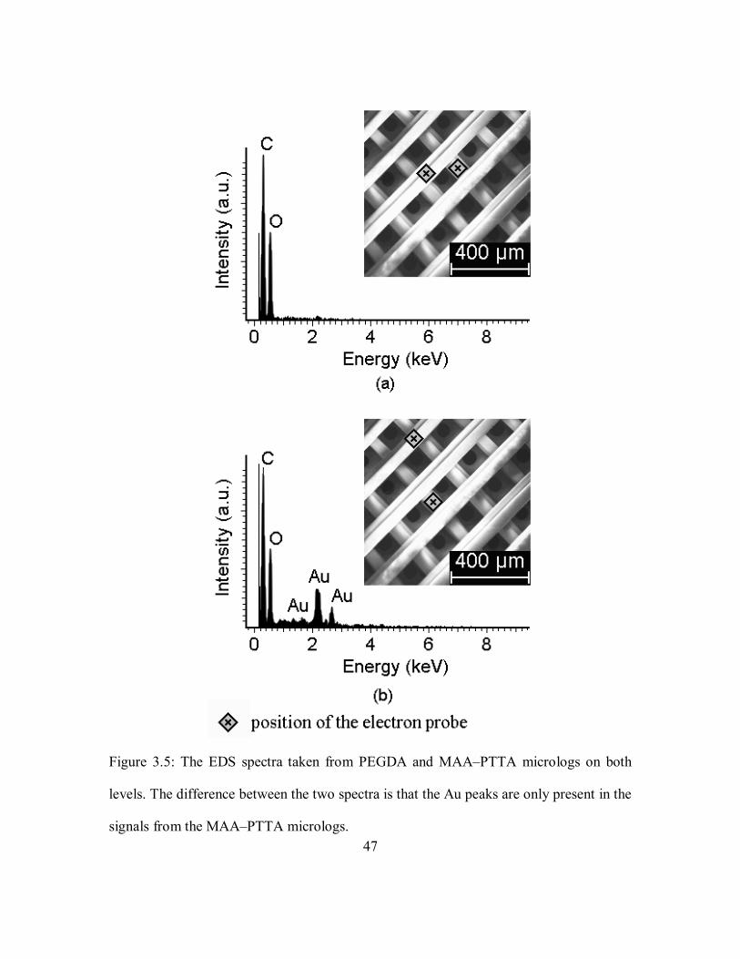
EDS analysis was carried out using a JEOL JSM-5610 scanning electron microscope.
The spectra were recorded by placing the electron probe (20 kV) on the micrologs made
from different materials. Comparing Figures 3.5 (a) and (b), we see that the characteristic
peaks of gold are only present in the signal from the MAA–PTTA microlog. The same
EDS results were also obtained from the bottom level of the microstructure. Since the
EDS signal does not carry enough information about the chemical state, we also did an x-
ray photoelectron spectroscopy (XPS) measurement to further clarify our results. In
addition to its capability of analyzing the chemical state, the XPS has a much lower
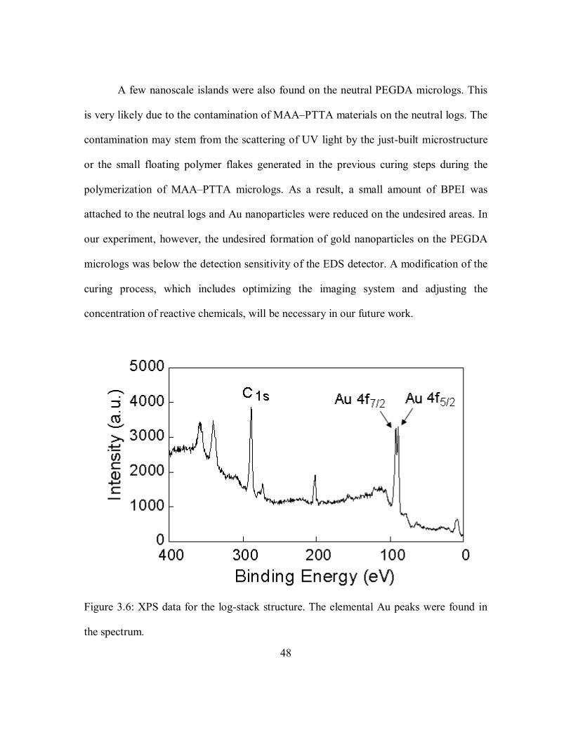
detection depth (<10 nm) than the EDS. In this case, it is especially helpful for
identifying those nanoscale features on the surface of the MAA–PTTA logs. Figure 3.6
shows the XPS data of the sample obtained using a Physical Electronics 5500TM XPS
system with an Al Kα x-ray source generating photons at an energy of 1486.6 eV. The
two elemental Au signals, the Au 4f7/2 peak and the Au 4f5/2 peak, found at binding
energies of 83.7 eV and 87.5 eV respectively, provided complementary evidence in
confirming the formation of the gold nanoparticles.
47
Figure 3.5: The EDS spectra taken from PEGDA and MAA–PTTA micrologs on both
levels. The difference between the two spectra is that the Au peaks are only present in the
signals from the MAA–PTTA micrologs.
48
A few nanoscale islands were also found on the neutral PEGDA micrologs. This
is very likely due to the contamination of MAA–PTTA materials on the neutral logs. The
contamination may stem from the scattering of UV light by the just-built microstructure
or the small floating polymer flakes generated in the previous curing steps during the
polymerization of MAA–PTTA micrologs. As a result, a small amount of BPEI was
attached to the neutral logs and Au nanoparticles were reduced on the undesired areas. In
our experiment, however, the undesired formation of gold nanoparticles on the PEGDA
micrologs was below the detection sensitivity of the EDS detector. A modification of the
curing process, which includes optimizing the imaging system and adjusting the
concentration of reactive chemicals, will be necessary in our future work.
Figure 3.6: XPS data for the log-stack structure. The elemental Au peaks were found in
the spectrum.

49
Since PEI can serve as both a reducing agent and a surfactant for the synthesis of
many metallic nanoparticles, a wide variety of materials in nanoscale form can be
localized three dimensionally on the polymer structure. This is to be shown in the next
section. Moreover, spatially selective growth of other nanostructures, such as nanowires,
grown from nanoparticle seeds may also be achieved. The resolution is solely defined by
the smallest feature that the DPP technique can fabricate without incorporating
impurities, depending on the precision of the optical projection system. So far we have
been able to achieve a line width of 10 μm with our current setup and material recipe.
3.4 WAVELENGTH SENSITIVE LIGHT-DRIVEN MICRO-TURBINE
3.4.1 Background Introduction
Electricity is not the only form of energy that light can be converted to. With
suitable media or devices, light can also be transformed to heat, chemical potential and
mechanical energy. Invented in the 19th century by British scientist Sir William Crookes,
Crookes radiometer, also known as the light mill, was one of the devices that convert
light into kinetic energy [23, 24]. Shown in Figure 3.7(a), the radiometer has four vanes
on a low friction spindle, sealed in a light bulb under certain vacuum condition. The
vanes are all white on one side, black on the other. When irradiated by the light, the dark
side absorbs more light energy and heat up the surrounding gas molecules faster than the
bright side. This causes a convection due to the temperature gradient across each vane
and creates a torque that drives the spindle. When heating is terminated, the device will
gradually stop rotating and then start to spin in the opposite direction until the system
reaches a new equilibrium. Because of the simple structure and the ease of manipulation,
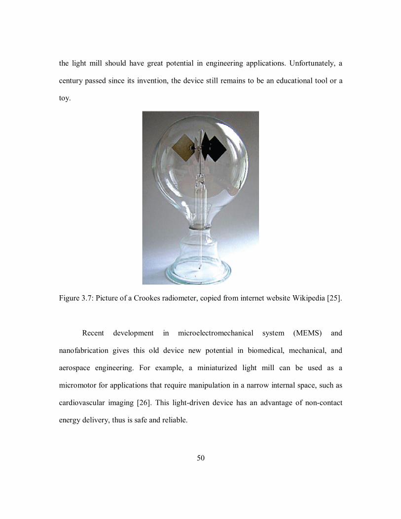
50
the light mill should have great potential in engineering applications. Unfortunately, a
century passed since its invention, the device still remains to be an educational tool or a
toy.
Figure 3.7: Picture of a Crookes radiometer, copied from internet website Wikipedia [25].
Recent development in microelectromechanical system (MEMS) and
nanofabrication gives this old device new potential in biomedical, mechanical, and
aerospace engineering. For example, a miniaturized light mill can be used as a
micromotor for applications that require manipulation in a narrow internal space, such as
cardiovascular imaging [26]. This light-driven device has an advantage of non-contact
energy delivery, thus is safe and reliable.

51
3.4.2 Fabrication Procedure
Using the digital photopolymerization technique and 3D selective nanoparticle
coating method described in the last section, we have successfully fabricated such a
miniatured device, displayed in Figure 3.8 (b). The structure of the micro-device is
approximately the same as the Crookes radiometer except the vanes. The four vanes of
device have a curved shape and directly branches from the central axis, which makes it
more like a micro-turbine. It has been proved that the curved geometry of the micro-
turbine’s blades, upon exposure to light radiation, can also generate a temperature
gradient across each blade due to the different heating rates between the convex and the
concave sides [27]. For the same reason, the micro-turbine is driven by the convection at
certain vacuum level.
Figure 3.8: (a) Cross sectional pattern used in the fabrication of the micro-turbine. (b)
Picture of a nanoparticle coated micro-turbine device.
52
The experiment setup for the fabrication of the micro-turbine was the same as the
one described in section 3.3.3 except that the pattern on the DMD chip was the cross
section of the micro-turbine, schematically illustrated in Figure 3.8 (a). The liquid
monomer used in the DPP process was 2:3 MMA and PTTA mixed with 2% of Irgacure
651 (Ciba Chemistry), 0.02% of TEMPO (Sigma-Aldrich), 0.1% of Tinuvin 234 (Ciba
Chemistry). Irgacure 651 is a photo-initiator which causes cross-linking among the
acrylate groups of MMA and PETA. TEMPO is a UV quencher, which acts as a
threshold for the polymerization. It controls the contrast of a UV pattern in the monomer.
Tinuvin 234 is a UV absorber. The amount of Tinuvin 234 determines the depth of UV
light projected in the monomer. It minimizes the contamination on the old structures
during the curing process of a new layer. In order to achieve a thickness of 100μm for
each repeating layer, the power of the UV projection was approximately set at
10mW/cm2. The exposure time for each layer was 25 seconds. For more detailed
description of the fabrication methods, please refer to Li-Hsin Han’s Ph.D. Dissertation
[28].
Two identical micro-turbines were built to be coated with gold and silver
nanoparicles respectively. They were then immersed in 1% Branched poly(ethylenimine)
(BPEI, Sigma-Aldrich, MW: 800) for 4 hours. After rinsed with de-ionic (DI) water, the
two micro-turbines were transferred to a flask containing 0.7 mM HAuCl4 aqueous
solution and a flask with 0.1M AgNO3 aqueous solution respectively. The flasks were
kept in the oil-bath at 85oC for 15 minutes. The colors of the two micro-devices both
turned dark soon after the flasks were heated up, indicating the reduction of nanoparticles

53
on the surface of the blades. The dark color of the micro-turbine can been seen in Figure
3.8 (b).
High resolution SEM images of the micro-turbines (not shown) showed that the
average diameter of the nanoparticles was approximately 50 nm.
3.4.3 Measurement Details
As can been seen in Figure 3.8 (b), each of the micro-turbines had a pin-shaft as
its axle. The pin-shaft was 400 μm in diameter and had pin-heads at both ends. It was
inserted through the center hole after the fabrication of the nanoparticle coated device.
The two micro-turbines with the pin-shafts were then mounted in a device holder with
each end of the pin-shafts inserted in a pivot-socket. This allowed the micro-turbine to
only spin around the axle with minimal friction. The device holder carrying the two
micro-turbines was placed in the glass vacuum chamber, as illustrated in Figure 3.9. A
mechanical pump was used to create partial vacuum in the chamber and the pressure was
controlled by a needle valve. The movement of the blades was detected by a laser
position sensor, which uses optical triangulation to measure the displacement of the
targeting object. The laser was targeting at one of the four blades. As the turbine spins,
the targeting blade moves out of the position and the one behind it enters the detecting
range. This creates a pulse signal in the position sensor. An oscilloscope was connected
to the sensor to record the signal so that the rotation speeds of the micro-turbines could be
calculated.

54
Figure 3.9: Top view of the measurement set up.
Three different optical filters were placed in front of a white light source one after
the other to observe the responses of the two devices under the irradiation of different
frequency range. The spectra of the light, after passing through the three filters, were
recorded in Figure 3.10. At certain white light intensity, three different working states
were achieved with each corresponding to the presence of one of three filters. With filter
a (spectrum shown in Figure 3.10 (a)), the micro-turbine coated with goldnanoparticles
stayed stationary while the one coated with silver nanoparticles rotated as fast as 1000
RPM. If we define motionlessness of the turbine as 0 and the spinning as 1, this can be
regarded as working state (0, 1). With filter b (spectrum shown in Figure 3.10 (b)), the
result was the opposite. Only the device coated with Au nanoparticles was spinning.

55
Under the band pass filter (spectrum shown in Figure 3.10 (c)) with the band centered at
650 nm, both of the micro-turbines rotated, representing a working state of (1, 1).
(a)
(b)

56
(c)
Figure 3.10: Spectra of (a) high-pass optical filter a, (b) band-pass optical filter b, (c)
low-pass filter c.
A simplified model was built to roughly describe the behavior of the micro-
turbine, although only numeric simulation may present the results more accurately. The
relation between the irradiation and rotation speed was described by
)(21
02 TTBII tbi (3.1)
where Ii is the power of the incident light, α is the absorption coefficient of the
nanoparticles, τ is friction constant of the needle, ω is the angular velocity of the micro-
turbine, I is the moment of inertia, B is heat transfer constant. By measuring the rotation
speed at different illumination levels using band-pass filters centered at different
wavelength, we were able to obtain α as a function of the center wavelength of the optical
filters, shown in Figure 3.11. In the same figure, the absorption of a 50nm spherical

57
nanoparticle simulated by COMSOL Multiphysics was also shown as a comparison. The
measured data fit the absorption rate obtain by simulation well.
Figure 3.11: Absorption rate of calculated (solid curve) and measured (dots) 50 nm Ag
and Au nanoparticles on polymer material.
The measured absorption rates appeared to be red-shifted and much broader
compared to the simulated results. This is very likely due to the extremely short distance
between the nanoparticles, since the concentration of the particles was very dense on the
surface of blades. There are also some other factors that may cause the discrepancy. First
of all, the measured data were not taken using monochromatic light. The spectra of each
band-pass filers were very broad. Secondly, polymer material also has considerable
absorption at short wavelength region and varying dielectric function throughout the
58
wavelength range of interests, resulting in higher measured values of the absorption rates.
Third, the model that was used to link measured rotation speed to the absorption rate
might be too rough. It is very difficult to find an analytical relation between the light
intensity and the rotation speed. A more accurate calculation can be found by computer
simulations [28].
3.5 SUMMARY
Nanoparticles of noble metals are good light absorbers near their surface
plasmons resonance frequencies. The absorbed photon energy is converted to heat,
increasing the temperature of the nanoparticles and the surrounding environment. Since
the absorption rate varies with the wavelength of the illuminating light, this phenomenon
can be used to realize a wavelength controlled light driven micro-tubine device.
Two identical micro-turbines were fabricated with polymer materials by digital
projection photopolymerization methed. The technique of three-dimensional selective
growth of metal nanoparticles on a polymer microstructure was developed in order to
coat gold and silver nanoparticles onto the blades of the two micro-turbines respectively.
The micro-turbine coated with gold nanoparticles has a different response wavelength
range from the one coated with silver particles. When the two devices were placed in the
same vacuum system, a combination of four on/off states was observed upon exposure to
the light irradiation through three different optical filters.
It is believed that the size, shape and even the composition of coated nanoparticles
can be controlled under different synthesis conditions such as the temperature of the
59
reduction process, the composition and concentration of the precursor solution, during the
three-dimensional selective localization process. Therefore, a fine tune of the wavelength
response of the micro-turbine is possible.
Reference
1. Mie, G. Ann. Phys. (Leipzig), 25, 377 (1908).
2. Cortie, M.; Xu, X.; Chowdhury, H.; Zareie, H. and Smith, G. "Plasmonic heating
of gold nanoparticles and its exploitation," Proc. SPIE, 5649, 565 (2005).
3. Arbouet, A.; Christofilos, D.; Del Fatti, N.; Vallée, F.; Huntzinger, J. R.; Arnaud,
L.; Billaud, P. and Broyer, M. "Direct Measurement of the Single-Metal-Cluster
Optical Absorption," Phys. Rev. Lett., 93, 127401 (2004).
4. Muskens, O. L.; Del Fatti, N.; Valléea, F.; Huntzinger, J. R.; Billaud,P. and
Broyer, M. "Single metal nanoparticle absorption spectroscopy and optical
characterization," Appl. Phys. Lett., 88, 063109 (2006).
5. Pissuwan, D.; Valenzuela, S. and Cortie, M. B. "Therapeutic possibilities of
plasmonically heated gold nanoparticles," Trends Biotechnol., 24, 62 (2006).
6. Klitzing, von K.; Dorda, G. and Pepper, M. "New Method for High-Accuracy
Determination of the Fine-Structure Constant Based on Quantized Hall," Phys.
Rev. Lett., 45, 494 (1980).
7. Iijima, S. "Helical microtubules of graphitic carbon," Nature, 354, 56 (1991).

60
8. Sun, Y. and Xia, Y. "Shape-Controlled Synthesis of Gold and Silver
Nanoparticles," Science, 298, 2176(2002).
9. Yan, H.; He, R.; Pham, J. and Yang, P. "Morphogenesis of Zinc oxide Nano- and
Micro-crystals," Adv. Mater., 15, 402 (2003).
10. Ashkin, A. and Dziedzic, J. M. "Optical Trapping and Manipulation of Viruses
and Bacteria," Science, 235, 1517 (1987).
11. Chu, S. "Laser Manipulation of Atoms and Particles," Science, 253, 861 (1991).
12. Yu, G.; Cao, A. and Lieber, C. M. "Large area blown bubble films of aligned
nanowires and carbon nanotubes," Nat. Nanotechnol., 2, 372 (2007).
13. McAlpine, M. C.; Ahmad, H.; Wang, D. and Heath, J. R. "Highly ordered
nanowire arrays on plastic substrates for ultrasensitive flexible chemical sensors,"
Nat. Mater., 6, 379 (2007).
14. Huang, J.; Fan, R.; Connor, S. and Yang, P. "One-step patterning of aligned
nanowire arrays by programmed dip coating," Angew. Chem. Int. Edn., 46, 2414
(2007).
15. Lu, Y. and Chen, S. "Direct write of microlens array using digital projection
photopolymerization," Appl. Phys. Lett., 92, 041109 (2008).
16. Note, C.; Kosmella, S. and Koetz, "Poly(ethyleneimine) as reducing and
stabilizing agent for the formation of gold nanoparticles in w/o microemulsions,"
J. Colloids Surf. A, 290, 150 (2006).
17. Tan, S.; Erol, M.; Attygalle, A.; Du, H. and Sukhishvili, S. "Synthesis of
Positively Charged Silver Nanoparticles via Oxidative Photoreduction of AgNO3

61
and Branched Polyethyleneimine in HEPES Solutions," Langmuir, 23, 9836
(2007).
18. Sun, X.; Dong, S. and Wang, E. "One-step polyelectrolyte-based route to well-
dispersed gold nano- particles: synthesis and insight," Mater. Chem. Phys., 96, 29
(2006).
19. Kreibig, U. and Vollmer, M. Optical Properties of Metal Clusters (Berlin:
Springer 1995).
20. Faraday, M. "Experimental Relations of Gold (and Other Metals) to Light," Phil.
Trans. R. Soc., 147, 145 (1857).
21. Eustis, S. and El-Sayed, M. A. "Why gold nanoparticles are more precious than
pretty gold: noble metal surface plasmon resonance and its enhancement of the
radiative and nonradiative properties of nanocrystals of different shapes," Chem.
Soc. Rev., 35, 209 (2006).
22. Farrer, R. A.; LaFratta, C. N.; Li, L.; Praino, J.; Naughton, M. J.; Saleh, B. E. A.;
Teich, M. C. and Fourkas, J. T. "Selective Functionalization of 3-D Polymer
Microstructures," J. Am. Chem. Soc., 128, 1796 (2006).
23. Einstein, A. "Zur Theorie der Radiometerkräfte," Z. Phys., 27, 1 (1924).
24. Maxwell, J. C. "On stresses in rarefied gases arising from inequalities of
temperature," Proc. R. Soc. London, 27, 304 (1878).
25. WIKIPEDIA. (Online) http://en.wikipedia.org/wiki/Crookes_radiometer.
26. Fercher, A. F.; Drexler, W.; Hitzenberger, C. K. and Lasser, T. "Optical
coherence tomography-principles and application," Rep. Prog. Phys., 66, 639
(2003).

62
27. Han, L.-H.; Wu, S.; Conduit, C.; Kemp, N.; Milner, T.; Feldman, M. and Chen,
S.C. "Light-Powered Micromotor Driven by Geometry-Assisted, Asymmetric
Photon-heating and Subsequent Gas Convection", Appl. Phys. Lett., 96 (21),
213509, (2010).
28. Han, L.-H., Ph.D. dissertation.

63
Chapter 4: Perforated Intermediate Electrode with Extraordinary
Optical Transmission in Novel Tandem Solar Cells
4.1 ABSTRACT
Another important plasmonic nanostructure is the subwavelength hole arrays
perforated on a metal film. The optical transmission through these nanometer scaled
apertures whose dimensions are smaller than the wavelength of the incident light can be
several orders of magnitude larger than expected. Previous studies have shown that the
enhanced transmission is due to the tunneling through surface plasmons. Based on this
property, a novel tandem solar cell structure was proposed. A metal film perforated with
periodic subwavelength hole arrays was inserted in a tandem solar cell as a light
transmittable intermediate common electrode for the top and the bottom cell. Similar to
conventional tandem solar cell structures, the top cell absorbs photons of short
wavelength and the bottom cell is to absorb light in long wavelength range. Being able to
transmit light through the subwavelength nanoapertures and conduct current
simultaneously, the perforated electrode allows electric power to be extracted from the
top and the bottom solar cell separately. This removes the current matching restriction in
the tandem device, eliminates the voltage drop across the junction of the sub-cells and
allows integration of different photoactive material systems in one device. The perforated
intermediate electrode was modeled and its optical performance in the tandem solar cell
was investigated.

64
4.2 EXTRAORDINARY OPTICAL TRANSMISSION THROUGH SUBWAVELENGTH HOLE
ARRAYS
Another important plasmonic nanostructure is the subwavelength hole arrays.
Light transmitting through a single hole is often accompanied by diffraction. The
classical diffraction theory describes this process very well. Take, for example, a circular
hole with radius r in an infinitely thin film. In the case of a large hole with respect to the
wavelength of the incident light (r >> λ), Huygens-Fresnel principle gives the far-field
transmitted light intensity I per unit solid angle.
21
22
0 sin)sin(2
4)(
krkrJrkII (4.1)
where θ is the angle between the direction of transmitted light wave and the normal of the
film, I0 is the intensity of the incident radiation impinging on the area of the circular hole
πr2, k is the wave number, J1(krsinθ) is the Bessel function of the first kind. This equation
is also known as the limit of Fraunhofer diffraction which describes a series of concentric
rings surrounding a bright spot in the center, called Airy pattern. The intensity of the total
transmitted light is given by
dIJ )( (4.2)
where Ω is the solid angle. Since r >> λ, J ≈ I0. This means that the transmission
coefficient T = J / I0 ≈ 1.
For a subwavelength aperture (r << λ), the above theory is no longer valid,
because it is based on the assumption of Kirchhoff’s scalar diffraction theory. In this

65
case, Bethe-Bouwkamp power law gives an analytical solution for the transmission
coefficient at normal incident condition [1].
42
2
4
271024
27)(64
rrkT (4.3)
One can see that the transmission coefficient scales with (r / λ)4, much smaller
than that calculated by the Kirchhoff theory. The above equation is based on two
assumptions. First, the film has zero thickness. Second, the conductivity of the film is
infinite, thus it is perfectly opaque. In reality, the aperture in the film with certain
thickness is a waveguide. It could allow propagating modes, causing a much higher
transmission coefficient. For metal screens with finite conductivities, they are only
opaque when the thickness is several times of the skin depth.
The transmission can also be dramatically enhanced through excitation of surface
plasmon polaritons (SPPs). The existence of SPP gives rise to a strong electromagnetic
field on the face of the metal screen at the incident side. After transmitting through the
aperture, the strong field is emitted at the other side of the film. Since light impinges on
the metal surface can be channeled into the aperture by propagating SPP, it is possible
that the transmission is larger than one (T > 1). The phenomenon that more light can
transmit through the subwavelength hole than that impinges on its area is called
extraordinary transmission, discovered by Ebbesen et al. [2]. In their work, a 200 nm
silver film was perforated with a square array of circular holes with a diameter of 150 nm
and a period of 900 nm. Extraordinary transmission, T > 1, was observed at wavelengths
larger than the period of the lattice, indicating the involvement of SPPs in the
transmission process. By changing the incident angle θ of the light and recording the

66
energy values corresponding to the transmission peaks, the dispersion relation of the
grating coupled surface plasmon polaritons can be plotted with respect to the momentum
kx = (2π/λ)sinθ along the [10] direction of the square hole array, as shown in Figure 4.1.
Figure 4.1: Dispersion relation of the grating coupled surface plasmon polaritons along
the [10] direction of the square hole array. The momentum kx is normalized to 2π/a0. [1]
Compared with the dispersion relation shown in Figure 1.3, the curves are
displaced by the grating vector G = 2π/a0 and a periodicity of 2π/a0 in kx can be expected.
Therefore, it can be assumed that the phase matching condition
0
2)(sin2)(a
nmnGmGkk yxxSP
(4.4)
67
where kSP is the propagation constant of the surface plasmon polaritons, m and n are
positive integers.
For normal incident radiation, the phase matching condition can be written as
0
2)(a
nmkSP
. Relating kSP with kx in equation 1.36 yields the wavelength of the
transmission peaks
22
0
22
0 )1(
nm
na
nm
a
(4.5)
where is the dielectric function of the metal screen and )1( n is the
effective index of the SPP in the case of metal/vacuum interface.
In recent years, it has been reported that the excitation of the localized surface
plamons may also cause the extraordinary transmission. Degiron et al. demonstrated the
optical transmission through a single subwavelength aperture in a free-standing silver
nano-film [2]. In their work, localized surface plasmons in the circular nano-hole was
confirmed by the emission excited with a high energy electron beam. Light transmission
through a single rectangular aperture was also studied. The dimension of the aperture
determines the spectral position and the number of the localized surface plasmon modes.
A later study also suggested that localized surface plasmons contribute to the
transmission through periodic subwavelength hole arrays [3]. García-Vidal et al. also
analyzed the transmission through a rectangular aperture in metal films [4]. Different
from the work by Degiron et al., the metal film in their work was modeled as a perfect
conductor. It was shown that enhanced transmission can also be attributed to the
resonance that is of surface plasmons.

68
The most straightforward applications of the extraordinary optical transmission
phenomena are frequency selective optical filters. By varying the shape of the holes or
applying external fields, tunable transmission can be achieved in terahertz band [5-7].
Porto et al. demonstrated optical bistability by filling non-linear materials into sub-
wavelength apertures, which can be regarded as optical switch [8]. Wenger et al. was
able to detect single molecule fluorescence in nanoapertures [9].
In the next section, we will introduce a new tandem solar cell design with high
transmission perforate metal film as an intermediate common electrode. The new design
breaks many limits of the conventional tandem cell structure. It is another example of
applying extraordinary transmission phenomenon in engineering problem.
4.3 NOVEL TANDEM SOLAR CELLS AND ITS INTERMEDIATE ELECTRODE
PERFORATED WITH SUBWAVELENGTH HOLE ARRAY
4.3.1 Background Introduction
In spite of tremendous progress made in the last century, improvements,
especially in reducing manufacturing cost and increasing energy conversion efficiency,
are still needed for photovoltaics to become an ideal substitution of fossil fuels energy in
the future. The exploitation of various nanomaterials and nanostructures is believed to be
a promising way to make significant contribution to the development of photovoltaics.
Taking the advantages of the unique optical properties of surface plasmons (SP), a great
deal of work has been done on modifying the light trapping or absorption in solar cells of
all kinds. Pioneering work includes the incorporation of small copper or silver clusters in
an organic solar cell by Stenzel and Westphalen [10, 11] in the late 1990s. The short

69
circuit current was doubled. Schaadt et al. [12] and Derkacs et al. [13] deposited gold
nanoparticles on wafer-based crystalline silicon solar cells and thin film amorphous
silicon solar cells respectively. Enhancement of both photocurrent and overall efficiency
was achieved. Recently, quite a few efforts have been made on the numerical analysis of
more sophisticated nanostructures to help understand the enhancement mechanism and
design novel plasmonic solar cells [14-18]. Almost all of the previous studies are based
on two major properties of the plasmonic nanostructures: near-field light concentration
and SP-enhanced light scattering.
Another important property of plasmonic nanostructures is the extraordinary
optical transmission (EOT) through array of subwavelength holes on an opaque metal
film. Since the discovery of this phenomenon by Ebbesen et al. [19] in 1998, both
theoretical research on underlying mechanisms [20-23] and proposed design of EOT
based optical devices [24, 25] have been actively reported. However, few applications
were found on photovoltaics. To author's knowledge, the only related work reported in
the past was by T. H. Reilly III and co-workers [26]. In their research, the possibility of
replacing the indium tin oxide (ITO) transparent electrode with a randomly perforated Ag
film in organic optoelectronics was demonstrated.
In the next section, a completely new tandem solar cell design with a periodically
perforated metal film as an intermediate electrode was introduced. Similar to
conventional tandem solar cell structures, the top cell absorbs photons of short
wavelength and the bottom cell is to absorb light in long wavelength range. The novelty
of this design lays in the insertion of this perforated metal film between the top and the
bottom solar cells. Being able to transmit light through the subwavelength nanoapertures

70
and conduct current simultaneously, the intermediate electrode can remove current
matching restriction, eliminate the voltage drop across the junction of the sub-cells, and
allow integration of different photoactive material systems in one device.
4.3.2 Computational Details
(a)
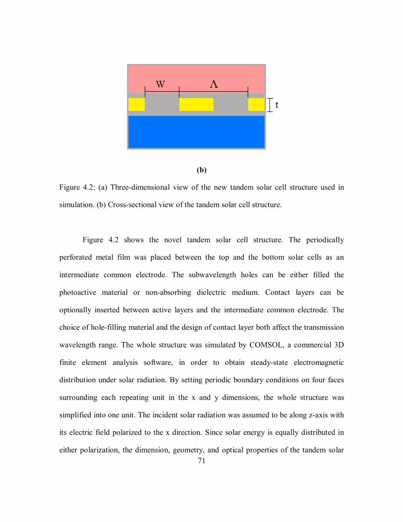
71
(b)
Figure 4.2: (a) Three-dimensional view of the new tandem solar cell structure used in
simulation. (b) Cross-sectional view of the tandem solar cell structure.
Figure 4.2 shows the novel tandem solar cell structure. The periodically
perforated metal film was placed between the top and the bottom solar cells as an
intermediate common electrode. The subwavelength holes can be either filled the
photoactive material or non-absorbing dielectric medium. Contact layers can be
optionally inserted between active layers and the intermediate common electrode. The
choice of hole-filling material and the design of contact layer both affect the transmission
wavelength range. The whole structure was simulated by COMSOL, a commercial 3D
finite element analysis software, in order to obtain steady-state electromagnetic
distribution under solar radiation. By setting periodic boundary conditions on four faces
surrounding each repeating unit in the x and y dimensions, the whole structure was
simplified into one unit. The incident solar radiation was assumed to be along z-axis with
its electric field polarized to the x direction. Since solar energy is equally distributed in
either polarization, the dimension, geometry, and optical properties of the tandem solar

72
cell structure and the subwavelength hole array were all set to be identical in both x and y
coordinate. Thus the optical performance of the nanostructure is independent to the
polarization of the incident light. Only one polarization needs to be considered
throughout this study. Perfectly matched layers (PML) were used to eliminate undesirable
reflection at the top and bottom boundaries of the simulation domain. The dielectric
constant data were taken from Ref. 27, 28 and 29. By integrating the Poynting vector
over the area of the photoactive layers boundaries, we were able to calculate the energy
flow across each interface and determine the wavelength range and the percentage of the
light that can penetrate the intermediate electrode and reach the bottom solar cell. The
tunability of the transmission wavelength range and bandwidth were also investigated in
order to optimize the performance of the solar cell.
4.3.3 Advantages of the New Tandem Solar Cell Design
The new tandem solar cell design has no difference from the conventional tandem
solar cell structure except the insertion of a perforated metal electrode between the top
and the bottom sub-cells. Similar to other tandem solar cell structures, the top solar cell is
to convert energy of the photons in short wavelength range into electric power. With the
unique properties of transmitting light in certain wavelength range, the metal film
perforated with subwavelength hole arrays allow long wavelength photons to penetrate
the metal and to be absorbed by the bottom solar cell. For conventional tandem solar
cells, a major constraint is that the photocurrent of each cell has to be the same because of
the top and the bottom cells are connected in series. As a result, degradation of one cell
will cause a bottleneck, limiting the current of the other and dramatically decreasing the

73
overall efficiency of the whole device. This often happens in Micromorph Si tandem cell,
where light-induced degradation of amorphous Si, also known as Staebler–Wronski
effect, is inevitable [30]. In out new design, the perforated metal film connects the top
and the bottom solar cell and acts an intermediate common electrode for both top and
bottom solar cells. Shown in Figure 4.3, the presence of the common electrode allows the
electric power to be retracted from the top and the bottom solar cells separately, thus
eliminating the current matching constriction. Without the current matching constriction,
the top and the bottom solar cell can be optimized independently in order to achieve a
maximum overall efficiency for the whole device.
Figure 4.3: Schematic illustration of the new tandem solar cell design.

74
Researchers at University of Delaware proposed spectrally and electrically
separated photovoltaic solar cells shown in Figure 4.4 [31]. In their design, sub-cells that
are used to absorb light with different wavelength range are placed in parallel on a
substrate. Expensive chromatic dispersion elements and optical condensers are used to
split and focus the light of different wavelength ranges to corresponding sub-cells. In our
design, the top and the bottom solar cells are also electrically separated. However, they
don't need to be spatially set apart. No extra optical apparatus is needed.
Figure 4.4: Schematic illustration of spectrally and electrically separated photovoltaic
solar cells [31].
In the case of conventional multi-junction solar cells, it takes considerable energy
for the carriers to transport from one sub-cell to another, decreasing the output voltage of
the solar cells. Therefore, tunnel junctions preferably made with wide bandgap material

75
are needed to allow electrons (holes) to transport from n (p) side to p (n) side [32] with
low resistance. However, the voltage drop across the junction is still inevitable even with
a high performance tunnel junction, let alone the difficulties of bandgap engineering to
minimize the heterojunction barriers. With the perforated metal film as the intermediate
common electrode, this price paid for charge transport through the sub-cells can be saved.
For demonstration purpose, poly (3-hexylthiophene) (P3HT)/6,6-phenyl C61-
butyric acid methyl ester (PCBM) blend, a widely used active material for organic solar
cells, was taken as the light absorbing layer for the top solar cell. Copper indium gallium
selenide (CIGS) was used as the active material for the bottom cell. A metal film with an
array of periodic subwavelength holes is sandwiched in between. The top and the bottom
sub-cells have completely different energy conversion and charge transport mechanisms.
In the top solar cell, excitons are generated in the polymer top cell upon exposure to the
solar light. The charges are separated when excitons diffuse to the donor-acceptor
interface. On the other hand, electron-hold pairs are created in the CIGS bottom cell and
are transported by the large built-in electric field across the PN junction. Without the
intermediate electrode to collect charge from the top and the bottom cells separately, it is
very difficult for these two kinds of materials to be used in the same device. This is
another advantage of this design.
In the next section, optical performance of the intermediate electrode will be
described. One will find that the perforate electrode may also enhance the absorption of
the top solar cell due to its light-trapping capability.
76
4.3.4 Optical Performance of Perforated Intermediate Electrode in Tandem Solar
Cells
Figure 4.5(a) shows three transmission curves, T1(λ), T2(λ), and T3(λ), for an 80
nm thick silver film with a periodic array of square shape holes sandwiched between a
100 nm thick P3HT:PCBM blend top solar cell and a 100 nm thick CIGS bottom solar
cell. The holes were 150 nm wide and have a period of 200 nm, filled with ITO. Another
20 nm ITO was inserted between the Ag intermediate electrode and the CIGS layer,
serving as the contact layer for the CIGS active region and the Ag electrode. The
structure is illustrated in the right inset of Figure 4.5 (a) with the interfaces of different
layers labeled for ease of the following description. The values of T1(λ), T2(λ), and T3(λ)
were defined as the ratio of power Pn(λ) flow through corresponding interfaces An.
T1(λ) = P3(λ) / P2(λ) (4.6)
T2(λ) = P4(λ) / P2(λ) (4.7)
T3(λ) = P4(λ) / P1(λ) (4.8)
T1(λ) curve is a direct indication of the percentage of the light power that can transmit
through the perforated electrode. The magnitude of the optical transmission, as can be
seen on the figure, did not follow Bethe-Bouwkamp power law which predicts that the
transmission scales as (1/λ)4 when the opening of the aperture are small than the
(effective) wavelength of the incident light [23]. Instead, with the area of the
subwavelength hole arrays covering only 56% of that of the whole intermediate
electrode, the maximum transmission reached nearly 100% at a wavelength of 670 nm.
This is a sign of the surface plasmon assisted extraordinary transmission. To further
verify this argument, the magnetic field magnitude |Hy| and the time averaged poynting

77
vectors at the peak transmission wavelength (670 nm) were plotted in the solar cell
model, shown in Figure 4.5(b). The observation of intense Hy field on the top surface of
the metal electrode supported the existence of plasmonic current, a clear indication of
surface plasmons excited the x-axis polarized incident light. The poynting vector plot
indicates the funneling of the power into the subwavelength aperture and the transmission
through the hole.
The T2(λ) curve in Figure 4.5(a) represents the percentage of the power enters the
bottom solar cell with respect to the power that flows out of the top solar cell. The values
are slightly smaller than T1(λ) due to the reflection at the ITO/CIGS interface. The
difference of T2(λ) and T3(λ) is the portion absorbed by the top cell.
(a)

78
(b) (c)
(d) (e)
Figure 4.5: (a) Optical transmission spectra T1(λ), T2(λ), and T3(λ), of the perforated Ag
electrode: t = 80 nm, W = 150 nm, Λ = 200 nm. T1 = P3 / P2, T2 = P4 / P2, T3 = P4 / P1.
Left inset: Optical absorption enhancement in the top polymer solar cell. Right inset: The
corresponding tandem cell structure with each interface labeled. (b) Cross-sectional view
of the magnetic field magnitude |Hy| in the solar cell model with poynting vectors plotted
79
together. (c) Optical transmission spectra T2(λ) for different width W of the
subwavelength holes at fixed period (Λ = 200 nm) and film thickness (t = 50 nm). (d)
Optical transmission spectra T2(λ) for different periodicities Λ. The film thickness and
the edge-to-edge distance of any two adjacent subwavelength holes remains the same in
this case (Λ - W = 50 nm, t = 50 nm). (e) Optical transmission spectra T2(λ) of the
perforated electrode with different thickness t (W = 150 nm, Λ = 200 nm).
The change of the light absorption in the top cell is shown in the left inset of
Figure 4.5(a). Compared with the case in which only the top cell is present, the
absorption in the top solar cell increased throughout nearly the whole absorption
wavelength range of the polymer material after the insertion of the perforated electrode.
The nanometer scaled features on the intermediate electrode is responsible for this
enhancement. They are capable of scattering light that is not completely absorbed by a
single path in the top cell and is not in the high transmission wavelength range of the
nanoaperture back to the top cell. This light trapping function adds another advantage for
the perforated electrode.
Figure 4.5(c) shows the transmission spectra T2(λ) of different hole sizes at fixed
film thickness and period. Smaller hole size corresponds to a longer peak transmission
wavelength. In Figure 4.5(d), the peak transmission wavelength remains the same as we
change the period of the subwavelength hole arrays. Note that in this case the edge-to-
edge distance (Λ - W) of any two adjacent nano-holes is fixed at 50 nm. It can be
concluded that the peak transmission wavelength of the intermediate electrode is tunable,
but it is only determined by the edge-to-edge distance of the nano-holes. This implies that

80
the extraordinary optical transmission in our nano-hole array structure is attributed to the
localized surface plasmon instead of the propagating surface plasmon polaritons. Because
of this, using different metal materials for the intermediate, such as gold and aluminum,
may also tune the wavelength of the maximum transmission. The tunability of the peak
transmission wavelength and the different choices of metal materials available both allow
the perforated electrode design to be generally applied to many other solar cell material
systems. The transmission spectrum can be easily adjusted by to fit the spectral
absorption rate of active material in the bottom solar cell for device optimization, and the
different metal material can be chosen if the electric performance of the electrode and the
metal/active layer interface needs to be considered.
Besides the wavelength tunability, another key data for the perforated electrode is the full
width at half maximum (FWHM) of the transmission curve. For the structure shown in
Figure 4.5 (a), it is about 120 nm. To maximize the absorption in the bottom solar cell,
the goal is to maximize the FWHM value while maintain a high the peak transmission
value. The data shown in Figure 4.5 (d) can also be used to observe how the optical
behavior of the perforated metal film will change when the dimension of nano-holes
varies. Figure 4.5 (e) shows the effect that adjusting thickness of the intermediate
electrode can bring to the electrode. One can see that a higher peak transmission can be
achieved either by increasing the size of the subwavelength holes or by reducing the
thickness of the electrode. As to increase the FWHM, the latter contributes more than the
former does. Some of the curves in Figure 4.5 appear to have transmission values greater
than one at certain wavelength. This is because the transmission T(λ) was not calculated
strictly based on its physical definition. In equations 4.6 - 4.8, the numerators were the
81
power flow across the corresponding interfaces of the tandem solar cell model, while the
denominators were all obtained in the case where only top polymer solar cell was present.
The purpose of using a single top polymer solar cell as a reference is to minimize the
difficulty in calculating the real transmission value in such a complicated structure with
multiple interfaces and to evaluate the absorption enhancement inside the polymer active
layer. The reflection at polymer/air interface in the case of a single top polymer solar cell
results in the calculated transmission larger than its real value.
Metal film with a thickness of only tens of nanometers has finite resistance. The
nanostructure corresponding to Figure 4.5 (a) has a sheet resistance of 0.6 Ω/sq, which is
not large enough to bring any advert effect to the electrical performance and energy
conversion efficiency of the solar cell. Expanding the dimension of the subwavelegth
holes and shrinking the thickness of the film both increase the sheet resistance of the
electrode linearly. To optimize the device performance, the optical and the electric
performance needs to be balanced.
4.4 SUMMARY
This chapter briefly described surface plasmon assisted extraordinary optical
transmission through subwavelength hole arrays on a metal film. While many efforts
have been devoted on incorporating nanostructures into solar cells by taking the
advantage of enhanced light scattering at surface plasmon resonance to improve the solar
energy conversion efficiency, application of high transmission subwavelength hole arrays
on this field remained intact.

82
We raised a brand new concept of using perforate metal film as intermediate
common electrode in a tandem solar cell. With the capability of transmitting low energy
photons from the top solar cell to the bottom one, the perforated intermediate electrode
allows the collection of electric power from the two sub-cells independently. This
immediately removes the current matching restriction of the two series-connected solar
cells, eliminates the voltage drop across the junction of the sub-cells, and allows
integration of different photoactive material systems in one device. At the same time, the
top cell also benefits from the enhanced light absorption due to the insertion of the
nanostructure underneath it.
Reference
1. Bouwkamp, C. J. Rep. Prog. Phys. 17, 35 (1954); Bethe, H. Phys. Rev. 66, 163
(1944).
2. Degiron, A.; Lezec, H. J.; Yamamoto, N.; and Ebbesen, T.W. "Optical transmission
properties of a single subwavelength aperture in a real metal", Opt. Commun. 239, 61
(2004).
3. Degiron, A. and Ebbesen, T.W. "The role of localized surface plasmon modes in the
enhanced transmission of periodic subwavelength apertures", J. Opt. A: Pure Appl.
Opt., 7 (2), S90 (2005).
4. García-Vidal, F. J.; Moreno, E.; Porto, J. A. and Martin-Moreno L. "Transmission of
Light through a Single Rectangular Hole", Phys. Rev. Lett., 95, 103901 (2005).

83
5. Battula, A. and Chen, S. C. "Extraordinary Transmission in a Narrow Energy Band
for Metallic Nano-gratings with Converging-Diverging Channels", Appl. Phys. Lett.,
89 (13), 131113 (2006).
6. Battula, A.; Chen, S. C.; Lu, Y.; Knize, R. J. and Reinhardt, K. "Tuning the
extraordinary optical transmission through subwavelength hole array by applying a
magnetic field", Optics Letters, 32 (18), 2692 (2007).
7. Battula, A.; Lu, Y.; Knize, R. J.; Reinhardt, K. and Chen, S. C. "Tunable
extraordinary optical transmission at 100 THz through a metallic hole array with a
varying hole shape", Opt. Express, 15 (22), 14629 (2007).
8. Porto, J. A.; Martin-Moreno, L. and García-Vidal, F. J. "Optical bistability in
subwavelength slit apertures containing nonlinear media," Phys. Rev. B, 70, 081402
(2004).
9. Wenger, J.; Lenne, P.-F.; Popov, E.; Rigneault, H.; Dintinger, J. and Ebbesen T.
"Single molecule fluorescence in rectangular nano-apertures," Opt. Express, 13 (18),
7035 (2005).
10. Stenzel, O.; Stendal, A.; Voigtsberger, K. and Borczykowski, C. V. "Enhancement of
the photovoltaic conversion efficiency of copper phthalocyanine thin film devices by
incorporation of metal clusters," Sol. Energy Mater. Sol. Cells, 37, 337 (1995).
11. Westphalen, M.; Kreibig, U.; Rostalski, J.; Lüth, H. and Meissner, D. "Metal cluster
enhanced organic solar cells," Sol. Energy Mater. Sol. Cells, 61, 97 (2000).
12. Schaadt, D. M.; Feng, B. and Yu, E. T. "Enhanced semiconductor optical absorption
via surface plasmon excitation in metal nanoparticles," Appl. Phys. Lett., 86, 063106
(2005).

84
13. Derkacs, D.; Lim, S. H.; Matheu, P.; Mar, W. and Yu, E. T. "Improved performance
of amorphous silicon solar cells via scattering from surface plasmons polaritons in
nearby metallic nanoparticles," Appl. Phys. Lett., 89, 093103 (2006).
14. Pala, R. A.; White, J.; Barnard, E.; Liu, J. and Brongersma, M. L. "Design of
Plasmonic Thin-Film Solar Cells with Broadband Absorption Enhancements," Adv.
Mater., 21, 1 (2009).
15. Catchpole, K. R. and Polman, A. "Design principles for particle plasmon enhanced
solar cells," Appl. Phys. Lett., 93, 191113 (2008).
16. Rockstuhl, C.; Fahr, S. and Lederer, F. "Absorption enhancement in solar cells by
localized plasmon polaritons," J. Appl. Phys., 104, 123102 (2008).
17. Ferry, V. E.; Sweatlock, L. A.; Pacifici, D. and Atwater, H. A. "Plasmonic
Nanostructure Design for Efficient Light Coupling into Solar Cells," Nano Lett., 8
(12), 4391 (2008).
18. Wang, W.; Wu, S.; Reinhardt, K.; Lu, Y. and Chen, S. C. "Broadband Light
Absorption Enhancement in Thin-Film Silicon Solar Cells," Nano Lett., 10 (6), 2012
(2010).
19. Ebbesen, T. W.; Lezec, H. J.; Ghaemi, H. F.; Thio, T. and Wolff, P. A.
"Extraordinary optical transmission through sub-wavelength hole arrays," Nature,
391, 667 (1998).
20. Martín-Moreno, L.; García-Vidal, F. J.; Lezec, H. J.; Pellerin, K. M.; Thio, T.;
Pendry, J. B. and Ebbesen, T.W. "Theory of Extraordinary Optical Transmission
through Subwavelength Hole Arrays," Phys. Rev. Lett., 86, 1114 (2001).
85
21. Cao, Q. and Lalanne, P. "Negative role of surface plasmons in the transmission of
metallic gratings with very narrow slits," Phys. Rev. Lett., 88, 057403 (2002).
22. Lalanne, P.; Hugonin, J. P. and Rodier, J. C. "Theory of surface plasmon generation
at nanoslit apertures," Phys. Rev. Lett., 95, 263902 (2005).
23. Lezec, H. J. and Thio, T. "Diffracted evanescent wave model for enhanced and
suppressed optical transmission through subwavelength hole arrays," Opt. Express,
12, 3629 (2004).
24. Battula, A.; Lu, Y.; Knize, R. J.; Reinhardt, K. and Chen, S. C. "Tunable transmission
at 100 THz through a metallic hole array with a varying hole channel shape," Opt.
Express, 15, 14629 (2007).
25. Wang, W.; Lu, Y.; Knize, R. J.; Reinhardt, K. and Chen, S. C. "Tunable and
polarization-selective THz range transmission properties of metallic rectangular array
with a varying hole channel shape", Opt. Express, 17 (9), 7361 (2009).
26. Reilly III, T. H.; Lagemaat, J. van de; Tenent, R. C.; Morfa, A. J. and Rowlen, K. L.
"Surface-plasmon enhanced transparent electrodes in organic photovoltaics," Appl.
Phys. Lett., 92, 243304 (2008).
27. Palik, E. D. Handbook of Optical Constants of Solids, 1, 290, (Academic, San Diego,
CA 1985).
28. Monestier, F.; Simon, J.-J.; Torchio, P.; Escoubas, L.; Flory, F.; Bailly, S.; Bettignies,
R. de; Guillerez, S. and Defranoux, C. "Modeling the short-circuit current density of
polymer solar cells based on P3HT:PCBM blend," Sol. Energy Mater. Sol. Cells, 91,
405 (2007).

86
29. Alonso, M. I.; Garriga, M.; Durante Rincon, C. A.; Hernandez, E. and Leon, M.
"Optical functions of chalcopyrite CuGaxIn1-xSe2 alloys," Appl. Phys. A, 74, 659
(2002).
30. Staebler, D. L. and Wronski, C. R. "Reversible conductivity changes in discharge-
produced amorphous Si," Appl. Phys. Lett., 31, 292 (1977).
31. Barnett, A.; Honsberg, C.; Kirkpatrick, D.; Kurtz, S.; Moore, D.; Salzman, D.;
Schwartz, R.; Gray, J.; Bowden, S.; Goosen, K.; Haney, M.; Aiken, D.; Wanlass, M.;
Emery, K.; Moriarty, and Kiehl, T. J. "50% Efficient Solar Cell Architectures and
Designs," 4th World Photovoltaic Science and Energy Conference, Hawaii, USA,
(2006).
32. Yamaguchi, M.; Takamoto, T. and Araki, K. "Super high-efficiency multi-junction
and concentrator solar cells. Energy Mater. Sol. Cells, 90, 3068 (2006).

87
Chapter 5: Conclusion and Outlook
Recent progress in nanotechnology has made the synthesis of numerous
nanomaterials and nanostructures possible. This significantly facilitated the fundamental
study of the material properties in nanometer scale. Interestingly, the discoveries of many
new phenomena from the latest research of nanoscience have been well described a few
decades ago. Plasmonics is one of the best examples. Neither of the two major
components of plasmonics, surface plasmon polaritons and localized surface plasmons,
fell out the scope of Maxwell’s equations. Their detailed properties and behaviors were
also clearly elucidated over 100 years ago. However, they did not catch too much
attention until the observation of those unexpected phenomena from various
subwavelength nanostructures in the past decade. Since then, many old theoretical topics
have been revisited and applied in the interpretation of the new phenomena and ideas of
novel applications have been actively proposed.
One of the important properties of localized surface plasmons is the enhanced
scattering cross-sectional area. At the surface plasmon resonance frequency, the
scattering cross section reaches a maximum and is much larger than the geometric size of
the scattering object. This is useful in improving the energy conversion efficiency of solar
cells. In Chapter 2, enhancement of light absorption in thin film solar cells by the
incorporation of two-dimensional periodic metal nanoparticle arrays was demonstrated.
Unfortunately, high absorption within the metal nanoparticle also occurs near the surface
plasmon resonance frequency region due to the interband transition. The intensity and the
bandwidth of the absorption enhancement in the solar cell were limited by the increased
88
absorption in the metal nanostructures. To further improve the efficiency of the solar
cells, engineering the shape and composition of the nanoparticle to minimize the overlap
of between the enhanced scattering and absorption might be a potential direction. The
strong scattering discussed in Chapter 1 does not rely on the assumption of metal
particles. Any subwavelength object may have this optical phenomenon. Enhanced
absorption due to the interband transition, however, is an exclusive property of metal
materials. This implies that it is not necessary to limit the application of enhanced
scattering to metal nanoparticles only.
On the other hand, for applications that require strong power dissipation within
the nanostructures, metal nanoparticles provide possibilities for wavelength selectivity. It
has been shown in Chapter 3 that nanoparticle coated light driven micro-turbines were
fabricated using a three-dimensional nanoparticle selective localization technique.
Compared with the one coated with silver nanoparticles, the micro-turbine coated with
gold particles exhibited different frequency response to the incident light. Thus,
controlling of the working states of multiple light driven micro-devices by wavelength
was achieved. A finer tuning of the wavelength response and polarization selectivity of
the micro-turbine could be possible, if the size, shape and even the composition of coated
nanoparticles can be controlled. This is achievable by altering the synthesis conditions
such as the temperature of the reduction process, the composition and concentration of
the precursor solution, during the three-dimensional selective localization process.
In Chapter 4, a new tandem solar cell structure was proposed. With a metal film
perforated with high optical transmission subwavelength hole arrays inserted between the
top solar cell and the bottom solar cell as an intermediate common electrode, charges can

89
be collected from the two sub-cells separately while long wavelength photons can still
transmit through the intermediate electrode. The addition of the high transmission
intermediate electrode removes the current matching restriction within the tandem device,
eliminates the voltage drop across the junction of the sub-cells, and allows integration of
different photoactive material systems in one device. The transmission wavelength range
can be tuned by adjusting the geometric parameters of the perforated film. This gives the
high transmission metal film the potentials of being applied in many other types of
tandem solar cell as an intermediate electrode. Having discussed the optical issues of new
design, the next step will be to deal with the fabrication techniques.
Overall, three major optical phenomena of the plasmonic nanostructures were
investigated. Applications of the unique properties of plasmonic nanostructures provide a
promising route in enhancing the energy conversion efficiency.

90
Bibliography
Akimov, Y. A. and Koh, W. S. "Resonant and nonresonant plasmonic nanoparticle enhancement for thin-film silicon solar cells," Nanotechnology, 21, 235201 (2010). Alonso, M. I.; Garriga, M.; Durante Rincon, C. A.; Hernandez, E. and Leon, M. "Optical functions of chalcopyrite CuGaxIn1-xSe2 alloys," Appl. Phys. A, 74, 659–664 (2002). Arbouet, A.; Christofilos, D.; Del Fatti, N.; Vallée, F.; Huntzinger, J. R.; Arnaud, L.; Billaud, P. and Broyer, M. "Direct Measurement of the Single-Metal-Cluster Optical Absorption," Phys. Rev. Lett., 93, 127401 (2004). Ashkin, A. and Dziedzic, J. M. "Optical Trapping and Manipulation of Viruses and Bacteria," Science, 235, 1517 (1987). Baba, K.; Okuno, T. and Miyagi, M. "Silver–gold compound metal island films prepared by using a two-step evaporation method," Appl. Phys. Lett., 62, 437 (1993). Barnett, A.; Honsberg, C.; Kirkpatrick, D.; Kurtz, S.; Moore, D.; Salzman, D.; Schwartz, R.; Gray, J.; Bowden, S.; Goosen, K.; Haney, M.; Aiken, D.; Wanlass, M.; Emery, K.; Moriarty, and Kiehl, T. J. "50% Efficient Solar Cell Architectures and Designs," 4th World Photovoltaic Science and Energy Conference, Hawaii, USA, (2006). Battula, A. and Chen, S. C. "Extraordinary Transmission in a Narrow Energy Band for Metallic Nano-gratings with Converging-Diverging Channels", Appl. Phys. Lett., 89 (13), 131113 (2006). Battula, A.; Chen, S. C.; Lu, Y.; Knize, R. J. and Reinhardt, K. "Tuning the extraordinary optical transmission through subwavelength hole array by applying a magnetic field", Optics Letters, 32 (18), 2692 (2007). Battula, A.; Lu, Y.; Knize, R. J.; Reinhardt, K. and Chen, S. C. "Tunable extraordinary optical transmission at 100 THz through a metallic hole array with a varying hole shape", Opt. Express, 15 (22), 14629 (2007). Bohren, C. F. and Huffman, D. R., Absorption and Scattering of Light by Small Particles, (Wiley-Interscience, New York, 1983). Boisdé, G. and Harmer, A. Chemical and biochemical sensing with optical fibers and waveguides, The Artech House optoelectronics library (Artech House, Boston, 1996). Bouwkamp, C. J. Rep. Prog. Phys. 17, 35 (1954); Bethe, H. Phys. Rev., 66, 163 (1944).

91
Catchpole, K. R. and Polman, A. "Design principles for particle plasmon enhanced solar cells," Appl. Phys. Lett., 93, 191113 (2008). Cao, Q. and Lalanne, P. "Negative role of surface plasmons in the transmission of metallic gratings with very narrow slits," Phys. Rev. Lett., 88, 057403 (2002). Choi, M.-R.; Stanton-Maxey, K. J.; Stanley, J. K.; Levin, C. S.; Bardhan, R.; Akin, D.; Badve, S.; Sturgis, J.; Robinson, J. P.; Bashir, R.; Halas, N. J. and Clare, S. E. "A Cellular Trojan Horse for Delivery of Therapeutic Nanoparticles into Tumors," Nano Letters, 7(12), 3759 (2007). Chu, S. "Laser Manipulation of Atoms and Particles," Science, 253, 861 (1991). Cortie, M.; Xu, X.; Chowdhury, H.; Zareie, H. and Smith, G. "Plasmonic heating of gold nanoparticles and its exploitation," Proc. SPIE, 5649, 565 (2005). Degiron, A. and Ebbesen, T.W. "The role of localized surface plasmon modes in the enhanced transmission of periodic subwavelength apertures", J. Opt. A: Pure Appl. Opt., 7 (2), S90 (2005). Degiron, A.; Lezec, H. J.; Yamamoto, N.; and Ebbesen, T.W. "Optical transmission properties of a single subwavelength aperture in a real metal", Opt. Commun. 239, 61 (2004). Derkacs, D.; Lim, S. H.; Matheu, P.; Mar, W. and Yu, E. T. "Improved performance of amorphous silicon solar cells via scattering from surface plasmons polaritons in nearby metallic nanoparticles," Appl. Phys. Lett., 89, 093103 (2006). Ebbesen, T. W.; Lezec, H. J.; Ghaemi, H. F.; Thio, T. and Wolff, P. A. "Extraordinary optical transmission through sub-wavelength hole arrays," Nature, 391, 667 (1998). Einstein, A. "Zur Theorie der Radiometerkräfte," Z. Phys., 27, 1 (1924). Eustis, S. and El-Sayed, M. A. "Why gold nanoparticles are more precious than pretty gold: noble metal surface plasmon resonance and its enhancement of the radiative and nonradiative properties of nanocrystals of different shapes," Chem. Soc. Rev., 35, 209 (2006). Faraday, M. "Experimental Relations of Gold (and Other Metals) to Light," Phil. Trans. R. Soc., 147, 145 (1857). Farrer, R. A.; LaFratta, C. N.; Li, L.; Praino, J.; Naughton, M. J.; Saleh, B. E. A.; Teich, M. C. and Fourkas, J. T. "Selective Functionalization of 3-D Polymer Microstructures," J. Am. Chem. Soc., 128, 1796 (2006).

92
Fercher, A. F.; Drexler, W.; Hitzenberger, C. K. and Lasser, T. "Optical coherence tomography-principles and application," Rep. Prog. Phys., 66, 639 (2003). Ferry, V. E.; Sweatlock, L. A.; Pacifici, D. and Atwater, H. A. "Plasmonic Nanostructure Design for Efficient Light Coupling into Solar Cells," Nano Lett., 8 (12), 4391 (2008). Fortina, P.; Kricka, L. J.; Graves, D. J.; Park, J.; Hyslop, T.; Tam, F.; Halas, N. J.; Surrey, S. and Waldman, S. A. "Applications of nanoparticles to diagnostics and therapeutics in colorectal cancer," Trends in Biotechnology, 24(4), 145 (2007). García-Vidal, F. J.; Moreno, E.; Porto, J. A. and Martin-Moreno L. "Transmission of Light through a Single Rectangular Hole", Phys. Rev. Lett., 95, 103901 (2005). Green, M. A. "Lambertian light trapping in textured solar cells and light-emitting diodes: analytical solutions," Progress in Photovoltaics: Research and Applications, 10, 235 (2002). Han, L.-H., Ph.D. dissertation. Han, L.-H.; Wang, W.; Lu, Y.; Knize, R. J.; Reinhardt, K.; Howell, J. R. and Chen, S. C. "Analytical and Experimental Investigation of Electromagnetic Field Enhancement among Nanospheres with Varying Spacing," Journal of Heat Transfer, 131, 033110 (2009). Han, L.-H.; Wu, S.; Conduit, C.; Kemp, N.; Milner, T.; Feldman, M. and Chen, S.C. "Light-Powered Micromotor Driven by Geometry-Assisted, Asymmetric Photon-heating and Subsequent Gas Convection", Appl. Phys. Lett., 96(21), 213509 (2010). Huang, J.; Fan, R.; Connor, S. and Yang, P. "One-step patterning of aligned nanowire arrays by programmed dip coating," Angew. Chem. Int. Edn., 46, 2414 (2007). Iijima, S. "Helical microtubules of graphitic carbon," Nature, 354, 56 (1991). Jackson, J.D. Classical Electrodynamics, 3rd edition, (John Wiley & Sons, New York 1999). Klitzing, von K.; Dorda, G. and Pepper, M. "New Method for High-Accuracy Determination of the Fine-Structure Constant Based on Quantized Hall," Phys. Rev. Lett., 45, 494 (1980). Kreibig, U. and Vollmer, M. Optical Properties of Metal Cluster, (Wiley, New York, 1995). Lalanne, P.; Hugonin, J. P. and Rodier, J. C. "Theory of surface plasmon generation at nanoslit apertures," Phys. Rev. Lett., 95, 263902 (2005).

93
Lezec, H. J. and Thio, T. "Diffracted evanescent wave model for enhanced and suppressed optical transmission through subwavelength hole arrays," Opt. Express, 12, 3629 (2004). Lu, Y. and Chen, S. "Direct write of microlens array using digital projection photopolymerization," Appl. Phys. Lett., 92, 041109 (2008). Martín-Moreno, L.; García-Vidal, F. J.; Lezec, H. J.; Pellerin, K. M.; Thio, T.; Pendry, J. B. and Ebbesen, T.W. "Theory of Extraordinary Optical Transmission through Subwavelength Hole Arrays," Phys. Rev. Lett., 86, 1114(2001). Maxwell, J. C. "On stresses in rarefied gases arising from inequalities of temperature," Proc. R. Soc. London 27, 304 (1878). McAlpine, M. C.; Ahmad, H.; Wang, D. and Heath, J. R. "Highly ordered nanowire arrays on plastic substrates for ultrasensitive flexible chemical sensors," Nat. Mater., 6, 379 (2007). Meier, J.; Spitznagel, J.; Kroll, U.; Bucher, C.; Fay, S.; Moriarty, T. and Shah, A. "High-efficiency amorphous and ‘micromorph’ silicon solar cells," Proceedings of the 3rd World Conference on PVSEC, Osaka, Japan, 3, 2801 (2003). Mergel D. and Qiao, Z. "Correlation of lattice distortion with optical and electrical properties of In2O3:Sn films," J. Phys. D, 35, 794 (2002). Mie, G. Ann. Phys. (Leipzig), 25, 377 (1908). Monestier, F.; Simon, J.-J.; Torchio, P.; Escoubas, L.; Flory, F.; Bailly, S.; Bettignies, R. de; Guillerez, S. and Defranoux, C. "Modeling the short-circuit current density of polymer solar cells based on P3HT:PCBM blend," Sol. Energy Mater. Sol. Cells, 91, 405 (2007). Muskens, O. L.; Del Fatti, N.; Valléea, F.; Huntzinger, J. R.; Billaud,P. and Broyer, M. "Single metal nanoparticle absorption spectroscopy and optical characterization," Appl. Phys. Lett., 88, 063109 (2006). Nie, S. and Emory, S. R., "Probing Single Molecules and Single Nanoparticles by Surface-Enhanced Raman Scattering," Science, 275, 1102 (1997). Note, C.; Kosmella, S. and Koetz, "Poly(ethyleneimine) as reducing and stabilizing agent for the formation of gold nanoparticles in w/o microemulsions," J. Colloids Surf. A, 290, 150 (2006).

94
Pala, R. A.; White, J.; Barnard, E.; Liu, J. and Brongersma, M. L. "Design of Plasmonic Thin-Film Solar Cells with Broadband Absorption Enhancements," Adv. Mater., 21, 1 (2009). Palik, E. D. Handbook of Optical Constants of Solids, 1, 290, (Academic, San Diego, CA 1985). Pillai, S.; Catchpole, K. R.; Trupke,T. and Green, M. A. "Surface plasmon enhanced silicon solar cells," J. Appl. Phys., 101, 093105 (2007). Pissuwan, D.; Valenzuela, S. and Cortie, M. B. "Therapeutic possibilities of plasmonically heated gold nanoparticles," Trends Biotechnol., 24, 62 (2006). Porto, J. A.; Martin-Moreno, L. and García-Vidal, F. J. "Optical bistability in subwavelength slit apertures containing nonlinear media," Phys. Rev. B, 70, 081402 (2004). Reilly III, T. H.; Lagemaat, J. van de; Tenent, R. C.; Morfa, A. J. and Rowlen, K. L. "Surface-plasmon enhanced transparent electrodes in organic photovoltaics," Appl. Phys. Lett., 92, 243304 (2008). Rockstuhl, C.; Fahr, S. and Lederer, F. "Absorption enhancement in solar cells by localized plasmon polaritons," J. Appl. Phys., 104, 123102 (2008). Schaadt, D. M.; Feng, B. and Yu, E. T. "Enhanced semiconductor optical absorption via surface plasmon excitation in metal nanoparticles," Appl. Phys. Lett., 86, 063106 (2005). Staebler, D. L. and Wronski, C. R. "Reversible conductivity changes in discharge-produced amorphous Si," Appl. Phys. Lett., 31, 292–294 (1977). Stenzel, O.; Stendal, A.; Voigtsberger, K. and Borczykowski, C. V. "Enhancement of the photovoltaic conversion efficiency of copper phthalocyanine thin film devices by incorporation of metal clusters," Sol. Energy Mater. Sol. Cells, 37, 337 (1995). Sun, X.; Dong, S. and Wang, E. "One-step polyelectrolyte-based route to well-dispersed gold nano-particles: synthesis and insight," Mater. Chem. Phys., 96, 29 (2006). Sun, Y. and Xia, Y. "Shape-Controlled Synthesis of Gold and Silver Nanoparticles," Science, 298, 2176 (2002). Tan, S.; Erol, M.; Attygalle, A.; Du, H. and Sukhishvili, S. "Synthesis of Positively Charged Silver Nanoparticles via Oxidative Photoreduction of AgNO3 and Branched Polyethyleneimine in HEPES Solutions," Langmuir, 23, 9836 (2007).

95
Wang, W.; Lu, Y.; Knize, R. J.; Reinhardt, K. and Chen, S. C. "Tunable and polarization-selective THz range transmission properties of metallic rectangular array with a varying hole channel shape", Opt. Express, 17 (9), 7361 (2009). Wang, W.; Wu, S.; Reinhardt, K.; Lu, Y. and Chen, S. C. "Broadband Light Absorption Enhancement in Thin-Film Silicon Solar Cells," Nano Lett., 10 (6), 2012 (2010). Wenger, J.; Lenne, P.-F.; Popov, E.; Rigneault, H.; Dintinger, J. and Ebbesen T. "Single molecule fluorescence in rectangular nano-apertures," Opt. Express, 13 (18), 7035 (2005). Westphalen, M.; Kreibig, U.; Rostalski, J.; Lüth, H. and Meissner, D. "Metal cluster enhanced organic solar cells," Sol. Energy Mater. Sol. Cells, 61, 97 (2000). Wu, S.; Wang, W.; Reinhardt, K.; Lu, Y. and Chen, S. C. "Absorption Enhancement in Thin Film Si Solar Cells by Two Dimensional Periodic Nanopatterns," Journal of Nanophotonics, accepted to publish. Xu, G.; Tazawa, M.; Jin, P.; Nakao, S. and Yoshimura, K. "Wavelength tuning of surface plasmon resonance using dielectric layers on silver island films," Appl. Phys. Lett., 82, 3811 (2003). Yamaguchi, M.; Takamoto, T. and Araki, K. "Super high-efficiency multi-junction and concentrator solar cells. Energy Mater. Sol. Cells, 90, 3068 (2006). Yan, H.; He, R.; Pham, J. and Yang, P. "Morphogenesis of Zinc oxide Nano- and Micro-crystals," Adv. Mater., 15, 402 (2003). Yu, G.; Cao, A. and Lieber, C. M. "Large area blown bubble films of aligned nanowires and carbon nanotubes," Nat. Nanotechnol., 2, 372 (2007). Zayats, A. V.; Smolyaninov, I. I. and Maradudin, A. A. "Nano-optics of surface plasmon polaritons," Physics Reports-Review Section of Physics Letters, 408, 131 (2005).

96
Vita
Shaomin Wu 吴绍敏was born in Shanghai, China on October 31st, 1977, to
Kegong Wu 吴克功 and Weiyan Lu 陆卫延. After graduating from High School
Affiliated to Fudan University in 1996, he attended Fudan University. In the summer of
2001, he received his Bachelor of Science degree in Materials Science. The same year, he
came to the Unite States and entered the graduate school at University of Southern
California in Los Angeles. One year later, he transferred to University of California,
Santa Barbara and studied there under the supervision of Dr. John E. Bowers until he
received his Master's degree in Electrical and Computer Engineering in 2004. During
year 2004 to 2006, he worked as a material engineering for Applied Optoelectronics, Inc.
in Sugar Land, Texas. In 2006, he resigned his job and continued to pursue his Ph.D. in
Materials Science and Engineering program at The University of Texas at Austin.
Professor Shaochen Chen 陈绍琛 was his supervisor.
Shaomin married Hong Li 李虹 in 2004. Their son, Tony A. Wu 吴先韬, was
born in 2005.
Email address: [email protected]
Permanent address: 239 Daming Road, Shanghai, China 200080
This dissertation was typed by Shaomin Wu.