controlled three-dimensional polystyrene micro- and nano
TRANSCRIPT

RSC Advances
PAPER
Ope
n A
cces
s A
rtic
le. P
ublis
hed
on 2
4 A
pril
2018
. Dow
nloa
ded
on 1
2/20
/202
1 4:
46:0
7 PM
. T
his
artic
le is
lice
nsed
und
er a
Cre
ativ
e C
omm
ons
Attr
ibut
ion
3.0
Unp
orte
d L
icen
ce.
View Article OnlineView Journal | View Issue
Controlled three
aThe School of Engineering, Institute for M
Edinburgh, Robert Stevenson Road, Edinbur
ac.ukbSchool of Physics, Institute of Science, Sur
Ratchasima, 30000, ThailandcSUT CoE on Advanced Functional Materi
Technology, Nakhon Ratchasima, 30000, Th
† Electronic supplementary informa10.1039/c7ra13278f
Cite this: RSC Adv., 2018, 8, 15501
Received 12th December 2017Accepted 17th April 2018
DOI: 10.1039/c7ra13278f
rsc.li/rsc-advances
This journal is © The Royal Society of C
-dimensional polystyrene micro-and nano-structures fabricated by three-dimensional electrospinning†
M. Vong, a E. Speirs,a C. Klomkliang,a I. Akinwumi,a W. Nuansing bc
and N. Radacsi *a
The combination of electrospinning with extrusion based 3D printing technology opens new pathways for
micro- and nanofabrication, which can be applied in a wide range of applications. This simple and
inexpensive method has been proven to fabricate 3D fibrous polystyrene structures with controlled
morphology and micro- to nano-scale fibers diameter. The controllable movement of the nozzle allows
precise positioning of the deposition area of the fibers during electrospinning. A programmed circular
nozzle pattern results in the formation of controllable 3D polystyrene designed shapes with fiber
diameters down to 550 nm. The assembly of the fibrous structures starts instantaneously, and a 4 cm tall
and 6 cm wide sample can be produced within a 10 minutes electrospinning process. The product
exhibits high stability at ambient conditions. The shape, size, and thickness of fibrous polystyrene
structures can be easily controlled by tuning the process parameters. It is assumed that the build-up of
3D fibrous polystyrene structures strongly depends on charge induction and polarization of the
electrospun fibers.
Introduction
Electrospinning is a simple and efficient process to manufac-ture micro and nanosized bers. By applying high voltage toa polymeric solution, a Taylor cone is formed at the tip ofa metallic nozzle and nanobers are ejected from it.1,2 Charac-teristics of the electrospun bers, such as the nature of thepolymer, diameter, surface to volume ratio, porosity, pore-interconnectivity, length, shape and structure, are widelycontrollable.3–9 It is also a versatile technique that allowsmanufacturing of ceramic and composite bers.10–13 Hence,electrospinning has been researched for different applicationsin various elds due to its simplicity and promising potentials.Potential applications include areas in biomedicine (e.g. wounddressing, bone screw hole and drug delivery), biosensors,cosmetics, protective clothing, catalyst, ltration, adsorption(e.g. dye removal and chromatography), batteries and fuelcells.14–27
aterials and Processes, The University of
gh, EH9 3FB, UK. E-mail: n.radacsi@ed.
anaree University of Technology, Nakhon
als (SUT-AFM), Suranaree University of
ailand
tion (ESI) available. See DOI:
hemistry 2018
The electrospun bers are randomly aligned and come in theform of at two-dimensional (2D) non-woven mats because ofthe bending instability, inherent to electrospinning.1,2 Thus,research has been carried out to circumvent this chaotic 2Ddeposition. Near-eld electrospinning can be used to controlthe exact positioning of the bers onto the collector by elec-trospinning at a short distance between the metallic nozzle andthe collector.28 With this technique, precise deposition andintegration of oriented bers into functional devices is achiev-able.29,30 A three-dimensional (3D) structure is more desirablethan a 2D mat for some applications. A 3D electrospun scaffoldis benecial for bioengineering as it resembles the brousstructure of the natural extracellular matrix and providescontact guidance for cells.31,32 In a particular example, macro-scopic 3D electrospun tubes have been shown to be favorable tonervous regeneration without inducing degradation of thenerves due to mechanical stress.33 3D electrospun scaffold hasalso been constructed to provide good mechanical stress andbetter cell proliferation and migration in bone tissue engi-neering.34 In other elds of research, it has been used for energyapplications, where a composite material was fabricated from3D carbon nanobers non-woven,35 and ltration purpose,where 3D layering of the nanobers mat was shown to have anincreased lter quality than a single mat.36 It is still a challengeto obtain a 3D brous macrostructure via electrospinning butwe can distinguish four main approaches to achieve this.37 Themain methods are increasing the electrospinning time andstacking multiple layers of bers,38 post-treatment of the 2D
RSC Adv., 2018, 8, 15501–15512 | 15501

RSC Advances Paper
Ope
n A
cces
s A
rtic
le. P
ublis
hed
on 2
4 A
pril
2018
. Dow
nloa
ded
on 1
2/20
/202
1 4:
46:0
7 PM
. T
his
artic
le is
lice
nsed
und
er a
Cre
ativ
e C
omm
ons
Attr
ibut
ion
3.0
Unp
orte
d L
icen
ce.
View Article Online
non-woven mats,39 use of a template-assisted collector40 ordirect self-assembly of the electrospun polymer.41–44 Thesemethods either require several time-consuming steps to obtainthe 3D structure or have no control over the nal shape of the3D structure. Electrospinning of designed 3D structures can beachieved by combining traditional electrospinning with themaneuverability of extrusion based 3D printing. By usinga nozzle able to move in the x–y plane, movement and control ofthe deposition area during the electrospinning process ispossible.
In this paper, the fabrication of 3D structures made ofpolystyrene (PS) bers using 3D electrospinning, without anyauxiliary collecting templates or post-processing steps, isinvestigated. The study is done by designing a specic nozzlepattern using a computer-aided design (CAD) soware, followedby electrospinning of this structure. In this work, the nozzlefollows a circular pattern and the desired electrospun structureof reference is a hollow cylinder. The effects of the solutionproperties, polymer concentration, applied voltage, workingdistance, ow rate, and nozzle speed on the 3D structures shapeand bers morphology are investigated. It is observed that theimproper control of any of these parameters would prevent 3Dassembly of the electrospun polymer, and result in a at 2Ddeposition. The microscopic properties of the electrospunbers are investigated via Scanning Electron Microscopy (SEM)and the macroscopic shapes of the 3D structures are recorded.
ExperimentalMaterials
The polymer polystyrene (PS) was obtained from Sigma-Aldrich.The weight average molecular weight (Mw) of PS was 280 000.The solvents dimethylformamide (DMF) and tetrahydrofuran(THF) were acquired from Alfa Aesar and Fisher Scientic,respectively. DMF was 99% pure and THF was 99.5% pure. Theadditives phosphoric acid 85% in water (H3PO4) and ethanol(99.99%) (EtOH) were received from Acros Organics and FisherScientic, respectively.
All products were used without further purication.
Solution preparation
PS was dissolved in a solvent mixture of 1 : 1 by weight DMF/THF by stirring for 4 hours under ambient conditions.
Table 1 Summary of all electrospun solutions
CompositionPS concentration[wt%]
Additives [100 mLin 50 mL solution]
PS in 1 : 1 DMF/THF 15.0 N/A15.0 EtOH15.0 H3PO4
12.5 H3PO4
10.0 H3PO4
7.5 H3PO4
5.0 H3PO4
15502 | RSC Adv., 2018, 8, 15501–15512
Several concentrations were prepared: 5.0 wt%, 7.5 wt%,10.0 wt%, 12.5 wt% and 15.0 wt%. An amount of 100 mL ofadditives were then added (EtOH or H3PO4) to 50 mL of solu-tion. The different solutions prepared are summarized inTable 1. Each batch started from a fresh solution, and eachelectrospinning experiment ran for 10 minutes.
Electrospinning apparatus
The electrospinning apparatus was combined with extrusionbased 3D printing technology to allow for control of variouspatterns and electrospinning structures. The apparatus itself(see Fig. 1) (NovaSpider, CIC nanoGUNE, Spain) consists ofa syringe pump, a nozzle and a high voltage DC power supply.The nozzle is capable of movements in the x–y axis, witha resolution of 0.02 mm, while the collector (print bed) can beset along the z-axis. In this study, the nozzle head was movingalong the x–y axis while the collector plate was xed along the zaxis during the experiment, but could be changed at will.Therefore, the electrospinning process here will be referred toas ‘3D electrospinning’.
The collector plate held a sheet of aluminum foil connectedto the ground, and possibly to a negative voltage supply. Thesolution was loaded into a syringe whose needle was connectedto the positive power supply and had an inner diameter of 0.603mm. All experiments were carried out at room temperature,between 20–27 �C, and the relative humidity, measured bya temperature and humidity sensor (HumidiProbe, Pico Tech-nology, United Kingdom) was between 45–55%.
2D pattern design: gcode/slicer
The nozzle pattern was generated by using a Computer AidedDesign (CAD) soware (Onshape). The designed pattern wasa hollow cylinder of 5.5 cm. The model was exported as an STLle. The model was then processed with a 3D printing slicingsoware (Simplify3D) to get a gcode le readable by the 3Delectrospinner. The gcode is controlling the pattern of thenozzle, the moving speed of the nozzle, the working distanceand the ow rate of the syringe. The applied voltage to thenozzle was controlled on a separate power supply. The pattern(the movement of the nozzle) was rst xed to be a circularmotion of 5.5 cm, as seen in Fig. 2, and the time of experimentto 10 minutes.
Fig. 1 Photo (left) and schematic drawing (right) Y–Z plane of the 3Delectrospinner.
This journal is © The Royal Society of Chemistry 2018

Fig. 2 Pattern of the nozzle as seen by the 3D printing slicing software(Simplify3D). A circle of 5.5 cm was designed as the nozzle pattern.
Paper RSC Advances
Ope
n A
cces
s A
rtic
le. P
ublis
hed
on 2
4 A
pril
2018
. Dow
nloa
ded
on 1
2/20
/202
1 4:
46:0
7 PM
. T
his
artic
le is
lice
nsed
und
er a
Cre
ativ
e C
omm
ons
Attr
ibut
ion
3.0
Unp
orte
d L
icen
ce.
View Article Online
Characterization
Digital camera. The macroscopic shape of the 3D structureaer electrospinning was captured using a digital camera (EOS6D, Canon Inc., Japan). The electrospinning process of the 3Dstructures was captured with the same camera.
Scanning electron microscope (SEM). The shape and size ofthe electrospun PS bers were observed with a Scanning Elec-tron Microscope (SEM) (JSM-6010PLUS/LV, JEOL Ltd., Japan) atan accelerating voltage of +20 kV. Prior to observation, thesamples were coated with 20 nm of gold using a Sputter coater(Desk III, Denton Vacuum, USA). The diameters of the berswere measured with an image processing program (Fiji –
ImageJ). The mean diameter was typically taken using morethan 100 bers per sample.
Fig. 3 Growth process of the electrospun PS fibers 3D structure. Theelectrospinning was performed at a voltage of +12 kV, a workingdistance of 5 cm, a flow rate of 5.0 mL h�1 and at a nozzle movingspeed of 12.0 mm s�1 for 10 minutes. The 3D build-up starts after aninitial flat layer of fibers have been deposited onto the collector as seenin (a). The build-up follows the circular pattern of the nozzle, forminga hollow cylinder. (b)–(d) The 3D structure is already observable after 3minutes and the cylinder shape is followed during the whole 10minutes of electrospinning.
Results and discussionFormation mechanism of the 3D structure
The incorporation of additives during the electrospinning ofpolystyrene bers is essential for obtaining 3D structures.Under ambient conditions, PS solutions without additivesproduce at, 2D structures with electrospinning.41 AddingEtOH, as suggested by Sun et al.,42 still resulted in atstructures.
As previous studies have indicated, the mechanism behindthe self-assembly of electrospun bers is based on the rapidsolidication of the bers, which allows the structure to be self-standing, and the polarization and electrostatic induction of thedeposited bers.42,45 The top of the deposited mat gets nega-tively charged because of the strong electric eld. This negativetop then becomes a preferential deposition site and attracts thepositively charged jet coming out of the nozzle. As the bers atthe top of the layer have the same charge, they would naturallyrepel each other during the build-up and fabricate a non-compact structure. Using additives into the solution canincrease the polarizability of the electrospun bers, leading torepulsive forces between bers. As H3PO4 is more conductivethan EtOH,46,47 this would explain why the solution doped withH3PO4 gives 3D structures, while the solutions doped with EtOHor without any doping agent result in 2D (at) structures.Therefore, H3PO4 was used in this study as a doping agent. The
This journal is © The Royal Society of Chemistry 2018
static induction and polarization effect can be proven by usinga charged rod to attract or repel the electrospun bers. This testwas done under two different conditions: aer electrospinning,when the structure was already built up with the electric eldturned off, and during the electrospinning process, when thehigh voltage was still applied on the moving nozzle. The testaer electrospinning was carried out on a sample that waselectrospun for 3 minutes. It was observed that both a positivelyand negatively charged rod would attract the top of the depos-ited ber mat. This is in contrast with the work of Sun et al.,42
who stated that the bers would be attracted to the positive rodbut repelled by the negative rod. This difference in behaviormight be because the rods used in our study had a high voltage(�5 kV), powerful enough to induce a charge on the 3D struc-ture. It was also observed that the electrospun structures werebarely attracted or repelled by a charged rod twelve hours aerthe experiment. This could be another explanation for thedifference in results with previous works. This result shows theease of inducing a charge on the bers, during or right aerelectrospinning. In the second test, the charged rod was placedabout 1.5 cm above the collector, under the way of the circularpattern of the nozzle. Despite the additional charged rod, it wasobserved that the 3D structures would still be built up along thecircular pattern of the nozzle. The electrospun bers reacted tothe charged rod only when close to its vicinity. They wereattracted to the positively charged rod, being compacted to therod and slowly pulling it toward the collector where a shortcircuit would then occur (see video in ESI†). The bers couldstill be deposited onto the negatively charged rod however, theywould not be compacted on the rod, but rather self-standing asthey were repelled because of their similar charge with thenegative rod. This test conrms that during electrospinning, thetop of the 3D structure, including the bers that were justelectrospun, are immediately induced with a negative chargebecause of the high positive voltage at the nozzle. This explainswhy the charge induction effect is not limited to the rst layer ofelectrospun bers and why the 3D structures can be built uprelatively high.
The growth process of the electrospun 3D structure wasrecorded using a digital camera. Pictures at different timeinterval are shown in Fig. 3, more time intervals can be seen inthe ESI S1† and its associated video. The 3D build-up of
RSC Adv., 2018, 8, 15501–15512 | 15503
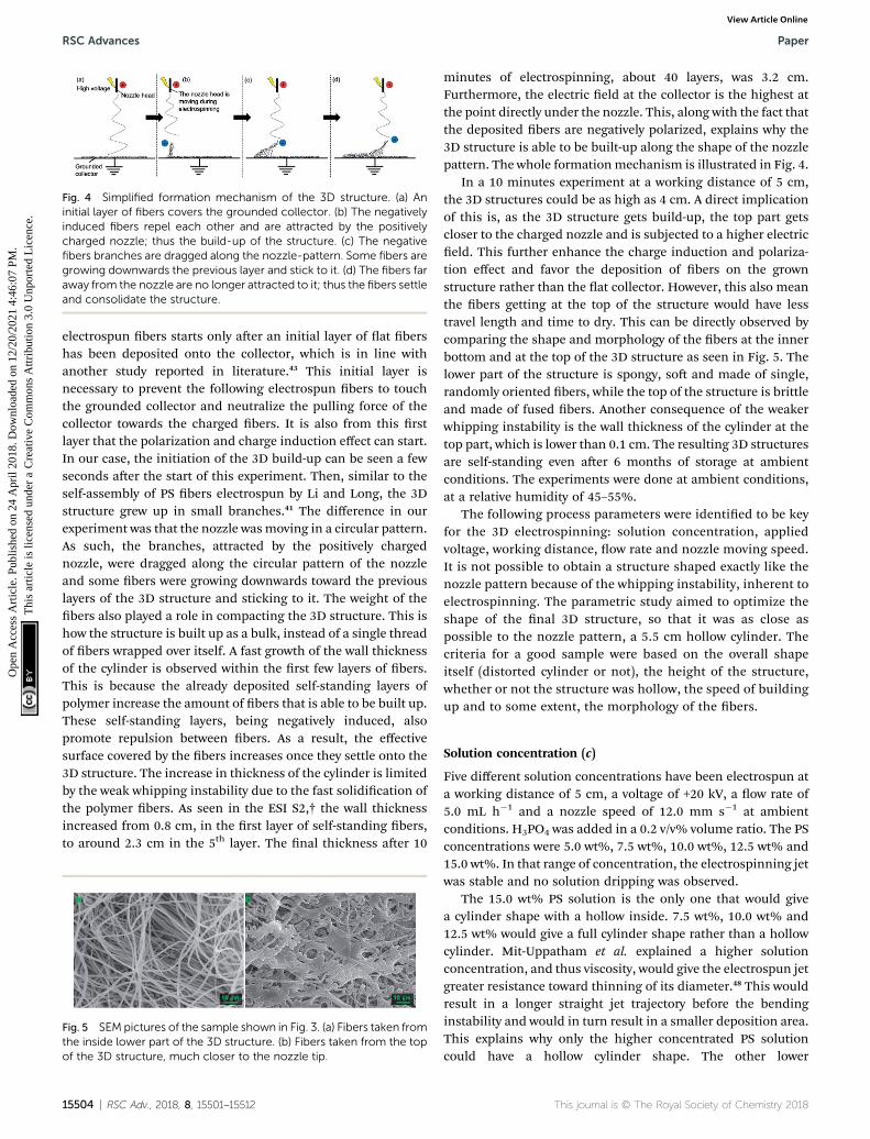
Fig. 4 Simplified formation mechanism of the 3D structure. (a) Aninitial layer of fibers covers the grounded collector. (b) The negativelyinduced fibers repel each other and are attracted by the positivelycharged nozzle; thus the build-up of the structure. (c) The negativefibers branches are dragged along the nozzle-pattern. Some fibers aregrowing downwards the previous layer and stick to it. (d) The fibers faraway from the nozzle are no longer attracted to it; thus the fibers settleand consolidate the structure.
RSC Advances Paper
Ope
n A
cces
s A
rtic
le. P
ublis
hed
on 2
4 A
pril
2018
. Dow
nloa
ded
on 1
2/20
/202
1 4:
46:0
7 PM
. T
his
artic
le is
lice
nsed
und
er a
Cre
ativ
e C
omm
ons
Attr
ibut
ion
3.0
Unp
orte
d L
icen
ce.
View Article Online
electrospun bers starts only aer an initial layer of at bershas been deposited onto the collector, which is in line withanother study reported in literature.43 This initial layer isnecessary to prevent the following electrospun bers to touchthe grounded collector and neutralize the pulling force of thecollector towards the charged bers. It is also from this rstlayer that the polarization and charge induction effect can start.In our case, the initiation of the 3D build-up can be seen a fewseconds aer the start of this experiment. Then, similar to theself-assembly of PS bers electrospun by Li and Long, the 3Dstructure grew up in small branches.41 The difference in ourexperiment was that the nozzle wasmoving in a circular pattern.As such, the branches, attracted by the positively chargednozzle, were dragged along the circular pattern of the nozzleand some bers were growing downwards toward the previouslayers of the 3D structure and sticking to it. The weight of thebers also played a role in compacting the 3D structure. This ishow the structure is built up as a bulk, instead of a single threadof bers wrapped over itself. A fast growth of the wall thicknessof the cylinder is observed within the rst few layers of bers.This is because the already deposited self-standing layers ofpolymer increase the amount of bers that is able to be built up.These self-standing layers, being negatively induced, alsopromote repulsion between bers. As a result, the effectivesurface covered by the bers increases once they settle onto the3D structure. The increase in thickness of the cylinder is limitedby the weak whipping instability due to the fast solidication ofthe polymer bers. As seen in the ESI S2,† the wall thicknessincreased from 0.8 cm, in the rst layer of self-standing bers,to around 2.3 cm in the 5th layer. The nal thickness aer 10
Fig. 5 SEM pictures of the sample shown in Fig. 3. (a) Fibers taken fromthe inside lower part of the 3D structure. (b) Fibers taken from the topof the 3D structure, much closer to the nozzle tip.
15504 | RSC Adv., 2018, 8, 15501–15512
minutes of electrospinning, about 40 layers, was 3.2 cm.Furthermore, the electric eld at the collector is the highest atthe point directly under the nozzle. This, along with the fact thatthe deposited bers are negatively polarized, explains why the3D structure is able to be built-up along the shape of the nozzlepattern. The whole formationmechanism is illustrated in Fig. 4.
In a 10 minutes experiment at a working distance of 5 cm,the 3D structures could be as high as 4 cm. A direct implicationof this is, as the 3D structure gets build-up, the top part getscloser to the charged nozzle and is subjected to a higher electriceld. This further enhance the charge induction and polariza-tion effect and favor the deposition of bers on the grownstructure rather than the at collector. However, this also meanthe bers getting at the top of the structure would have lesstravel length and time to dry. This can be directly observed bycomparing the shape and morphology of the bers at the innerbottom and at the top of the 3D structure as seen in Fig. 5. Thelower part of the structure is spongy, so and made of single,randomly oriented bers, while the top of the structure is brittleand made of fused bers. Another consequence of the weakerwhipping instability is the wall thickness of the cylinder at thetop part, which is lower than 0.1 cm. The resulting 3D structuresare self-standing even aer 6 months of storage at ambientconditions. The experiments were done at ambient conditions,at a relative humidity of 45–55%.
The following process parameters were identied to be keyfor the 3D electrospinning: solution concentration, appliedvoltage, working distance, ow rate and nozzle moving speed.It is not possible to obtain a structure shaped exactly like thenozzle pattern because of the whipping instability, inherent toelectrospinning. The parametric study aimed to optimize theshape of the nal 3D structure, so that it was as close aspossible to the nozzle pattern, a 5.5 cm hollow cylinder. Thecriteria for a good sample were based on the overall shapeitself (distorted cylinder or not), the height of the structure,whether or not the structure was hollow, the speed of buildingup and to some extent, the morphology of the bers.
Solution concentration (c)
Five different solution concentrations have been electrospun ata working distance of 5 cm, a voltage of +20 kV, a ow rate of5.0 mL h�1 and a nozzle speed of 12.0 mm s�1 at ambientconditions. H3PO4 was added in a 0.2 v/v% volume ratio. The PSconcentrations were 5.0 wt%, 7.5 wt%, 10.0 wt%, 12.5 wt% and15.0 wt%. In that range of concentration, the electrospinning jetwas stable and no solution dripping was observed.
The 15.0 wt% PS solution is the only one that would givea cylinder shape with a hollow inside. 7.5 wt%, 10.0 wt% and12.5 wt% would give a full cylinder shape rather than a hollowcylinder. Mit-Uppatham et al. explained a higher solutionconcentration, and thus viscosity, would give the electrospun jetgreater resistance toward thinning of its diameter.48 This wouldresult in a longer straight jet trajectory before the bendinginstability and would in turn result in a smaller deposition area.This explains why only the higher concentrated PS solutioncould have a hollow cylinder shape. The other lower
This journal is © The Royal Society of Chemistry 2018

Fig. 6 Evolution of the 3D structures shape as the weight concentration of PS is increased from 5.0 wt% to 15.0 wt%. The solutions wereelectrospun at a voltage of +20 kV, a working distance of 5 cm, a flow rate of 5.0 mL h�1 and at a nozzle speed of 12.0 mm s�1 for 10 minutes. No3D build-up were observed at low polymer concentration. The shape of the 3D structure is influenced by the polymer concentration.
Paper RSC Advances
Ope
n A
cces
s A
rtic
le. P
ublis
hed
on 2
4 A
pril
2018
. Dow
nloa
ded
on 1
2/20
/202
1 4:
46:0
7 PM
. T
his
artic
le is
lice
nsed
und
er a
Cre
ativ
e C
omm
ons
Attr
ibut
ion
3.0
Unp
orte
d L
icen
ce.
View Article Online
concentrations had a deposition area big enough to partly coverthe inside of the cylinder. Another consequence of the widerdeposition area was the nal height of the 3D structure aer 10minutes of electrospinning. The 3D structures electrospun with7.5 wt% and 10.0 wt% PS were smaller in height than the onesprepared with 12.5 wt% and 15.0 wt% PS. Another explanationwould be the lower amount of polymer provided to the 3Dstructure, which would effectively result in a smaller 3D struc-ture aer the same time of experiment. The top of the smaller3D structures was also not brittle, as depicted in Fig. 6, as thetravel length was still sufficient for the bers to dry properly. Atthe lowest concentration of 5.0 wt%, the electrospun 3D struc-tures had no features. It is necessary to provide a signicantamount of bers at once to get a proper 3D build-up of the PSsolution. If not, the charge induction and polarization effectwould not be strong enough and this would result in a atdeposition of the electrospun bers, as there would be norepulsion between bers to get the 3D build-up. The resultingdeposition area was bigger than for the higher concentrations.As PS is a poor conductor, some charges were still retained bythe deposited bers and diverted the electrospinning jet toregions of lower resistance.49 The overall shapes of the 3D
Fig. 7 Evolution of themean fiber diameters as the PS concentration isincreased from 5.0 to 15.0 wt% in 1 : 1 DMF/THF. The electrospinningparameters were a voltage of +20 kV, a working distance of 5 cm,a flow rate of 5.0mL h�1 and a nozzlemoving speed of 12.0mm s�1 for10 minutes. Mean fiber diameter increases with the polymerconcentration.
This journal is © The Royal Society of Chemistry 2018
structures electrospun with different PS concentration solu-tions is summarized in Fig. 6.
The mean ber diameter increases with polymer concen-tration as seen in Fig. 7, the lesser concentrated PS solutiongiving smaller bers. The mean diameters as measured on SEMare 0.55 � 0.25 mm, 0.79 � 0.30 mm, 1.09 � 0.31 mm, 1.40 � 0.44mm and 1.87 � 0.34 mm for the 5.0 wt%, 7.5 wt%, 10.0 wt%,12.5 wt% and 15.0 wt% PS solution respectively. This trend hasbeen observed several times by other researchers.50–52 Theelectrospun jet of the lesser concentrated solutions couldstretch and thin more because of the lower viscosity, resultingin smaller bers. Even though the concentrations of 5.0 wt%and 7.5 wt% had bers diameters in the sub-micron scale, theseelectrospun solutions gave mixtures of bers and beads. Thistrend has been already observed,53,54 and as Lee et al. suggested,it might be due to the lower solution viscosity that leads to a lessstable jet formation.55 SEM pictures of the samples are availablein the ESI S3.†
The 15.0 wt% PS solution was selected, as it was the onlysolution yielding a hollow cylinder as designed in the nozzlepattern.
Applied voltage (V)
The effect of the applied voltage on the 3D structure was testedin a range of 6 kV to 20 kV, with increments of 1 kV. All the otherparameters were xed. The working distance was 5 cm, theowrate was 5.0 mL h�1, the nozzle speed was 12.0 mm s�1, and15.0% PS in 1 : 1 DMF/THF doped with H3PO4 was electrospunat ambient conditions. Examples of electric eld simulationsare shown for applied voltages of 7, 15 and 20 kV in the ESI S4.†
The electrospinning jet was not stable at +6 kV, resulting inlots of dripping of the solution. The 3D structures and stableelectrospinning were obtained when the applied voltage washigher than +7 kV.
A few differences were observed with the nal shape andheight of the resulting cylinders aer electrospinning. Only thesample made at +10 kV seemed to show a shape closer to thedesigned 5.5 cm diameter hollow cylinder, as its outer wall wasthinner and vertical. However, the time needed to go from a atelectrospinning to a clear 3D build-up decreased as the appliedvoltage increased. Typically, the 3D build-up would happen in
RSC Adv., 2018, 8, 15501–15512 | 15505

Fig. 8 Evolution of the mean fiber diameters as the voltage isincreased from +7 kV to 20 kV. 15.0 wt% PS in 1 : 1 DMF/THF waselectrospun at a working distance of 5 cm, a flow rate of 5.0 mL h�1, ata nozzle moving speed of 12.0 mm s�1 for 10 minutes. There wasa critical voltage at which point the mean fiber diameter wouldincrease again, up to a stable range after 18 kV.
RSC Advances Paper
Ope
n A
cces
s A
rtic
le. P
ublis
hed
on 2
4 A
pril
2018
. Dow
nloa
ded
on 1
2/20
/202
1 4:
46:0
7 PM
. T
his
artic
le is
lice
nsed
und
er a
Cre
ativ
e C
omm
ons
Attr
ibut
ion
3.0
Unp
orte
d L
icen
ce.
View Article Online
less than 20 seconds when the applied voltage was higher than+15 kV and a at electrospinning time of 4 minutes 30 secondswas necessary before the 3D structuring was observed at thevoltage of +8 kV. As explained earlier, the 3D build-up is due tothe polarization and static induction of the deposited mat. Ifa lower voltage is applied, more time would be necessary for thetop of the deposited mat to get properly polarized, acquireenough negative charges to attract the positively charged jet,and thus build-up the 3D structure.
The electrospun polymer, under SEM observation, showeda similar bers shape but different bers diameters. Themeasured mean diameters were 2.53 � 0.51, 1.65 � 0.42, 1.34 �0.27, 1.32 � 0.22, 1.29 � 0.26, 1.42 � 0.26, 1.61 � 0.23, 1.42 �0.26, 1.67 � 0.25, 1.44 � 0.24, 1.50 � 0.31, 1.89 � 0.63, 1.88 �0.41, 1.88 � 0.34 mm for the applied voltage from 7 to 20 kV,respectively (see Fig. 8). The effects of applied voltage on theber diameters is one of the most controversial and contra-dicted in electrospinning experiments. Electrospun bers havebeen observed to be thicker with both increasing voltage56–58
and decreasing voltage59,60 or having a critical voltage valuewhere the trend would be reversed.61 The applied voltage
Fig. 9 Evolution of the 3D structures shape as the voltage is increased fra working distance of 5 cm, a flow rate of 5.0 mL h�1, at a nozzle movinghad the closest representation to the designed cylinder, having thin wallsthat, the applied voltage had little influence on the cylinder shape.
15506 | RSC Adv., 2018, 8, 15501–15512
inuences the electric eld, which can have multiple effects onthe electrospun jet. In this study, at the working distance of5 cm, there was no linear trend between the mean ber diam-eter and the applied voltage. Instead, the ber diameter wasdecreasing until the voltage of +11 kV where it would thenincrease up to a stable range at voltages higher than +18 kV.This would mean that up to +11 kV, increasing the voltageresults in a stronger electric eld which would lengthen theelongation of the jet and decrease the ber diameters, byallowing more stretching and splitting of the bers.62 Furtherincreasing the voltage up to +18 kV could result on a decrease ofthe size of the initial Taylor cone or a higher jet velocity. Thesetwo reasons together can counteract the effect of the lengthenedjet and lead to bigger bers. At voltages between 18 kV and 20kV, the above mentioned effects might cancel out each other.
As minimal differences were observed with the nal shape ofthe electrospun cylinder (see Fig. 9), the high voltage of +20 kVwas chosen to minimize the time necessary before the start ofthe 3D build-up. This high voltage was also selected to makesure a stable electrospinning process could be obtained forfurther studies that would have required a higher workingdistance or a higher ow rate. Pictures and bers morphology ofthe samples electrospun at the other applied voltage are in theESI (Fig. S5 to S7†).
Working distance (WD)
Investigations on the inuences of working distance on the 3Dbuild-up were done at a ow rate of 5.0 mL h�1 and a nozzlespeed of 12.0 mm s�1. The voltage was xed at +20 kV for mostdistances except for the low working distance of 1 cm. A voltageof +10 kV was used for the working distance of 1 cm, this wasnecessary to avoid short circuit between the charged nozzle andthe collector plate.
Working distances above 10 cm would not result in a stable3D build-up. At WD 10 cm, a bers network between the movingnozzle belt and the collector plate is observed (see Fig. 10). AtWD 15 cm, the bers were only deposited on the nozzle col-lecting belt, and no structures were observed on the collectorplate. At high working distance, the nozzle collecting belt canact as a preferential collector because of its closer proximity to
om +7 kV to +20 kV. 15.0 wt% PS in 1 : 1 DMF/THF was electrospun atspeed of 12.0 mm s�1 for 10 minutes. The sample processed at +10 kVand the least amount of fibers coverage inside the cylinder. Other than
This journal is © The Royal Society of Chemistry 2018
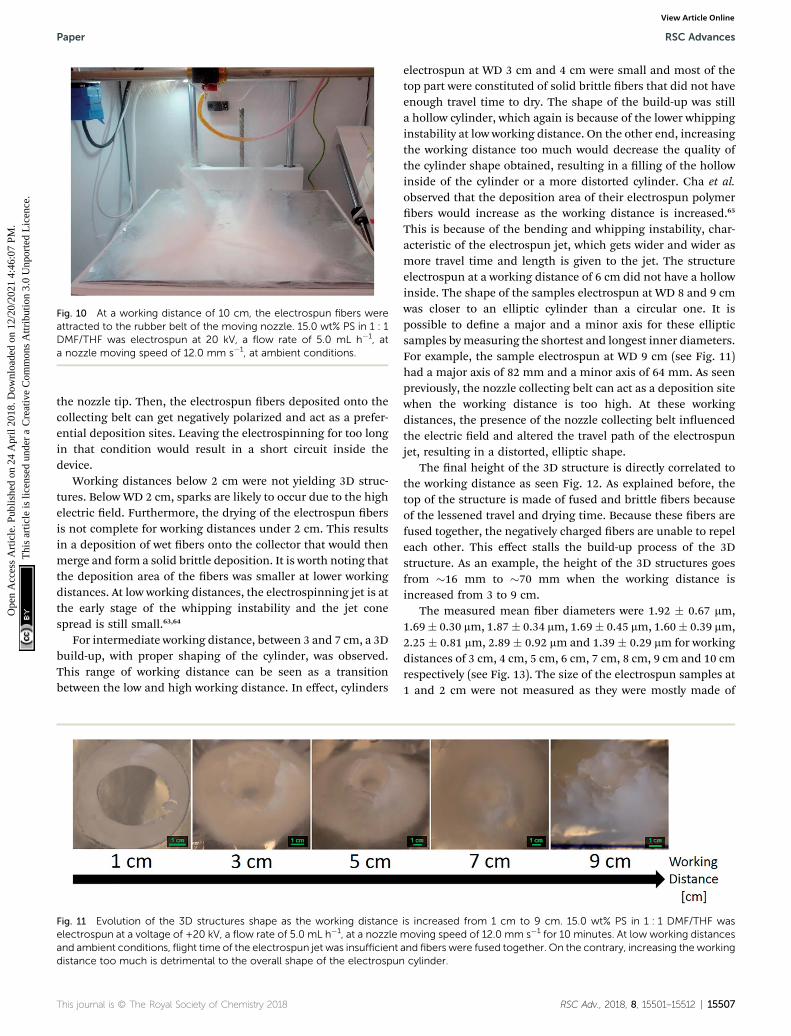
Fig. 10 At a working distance of 10 cm, the electrospun fibers wereattracted to the rubber belt of the moving nozzle. 15.0 wt% PS in 1 : 1DMF/THF was electrospun at 20 kV, a flow rate of 5.0 mL h�1, ata nozzle moving speed of 12.0 mm s�1, at ambient conditions.
Paper RSC Advances
Ope
n A
cces
s A
rtic
le. P
ublis
hed
on 2
4 A
pril
2018
. Dow
nloa
ded
on 1
2/20
/202
1 4:
46:0
7 PM
. T
his
artic
le is
lice
nsed
und
er a
Cre
ativ
e C
omm
ons
Attr
ibut
ion
3.0
Unp
orte
d L
icen
ce.
View Article Online
the nozzle tip. Then, the electrospun bers deposited onto thecollecting belt can get negatively polarized and act as a prefer-ential deposition sites. Leaving the electrospinning for too longin that condition would result in a short circuit inside thedevice.
Working distances below 2 cm were not yielding 3D struc-tures. Below WD 2 cm, sparks are likely to occur due to the highelectric eld. Furthermore, the drying of the electrospun bersis not complete for working distances under 2 cm. This resultsin a deposition of wet bers onto the collector that would thenmerge and form a solid brittle deposition. It is worth noting thatthe deposition area of the bers was smaller at lower workingdistances. At low working distances, the electrospinning jet is atthe early stage of the whipping instability and the jet conespread is still small.63,64
For intermediate working distance, between 3 and 7 cm, a 3Dbuild-up, with proper shaping of the cylinder, was observed.This range of working distance can be seen as a transitionbetween the low and high working distance. In effect, cylinders
Fig. 11 Evolution of the 3D structures shape as the working distanceelectrospun at a voltage of +20 kV, a flow rate of 5.0 mL h�1, at a nozzleand ambient conditions, flight time of the electrospun jet was insufficientdistance too much is detrimental to the overall shape of the electrospun
This journal is © The Royal Society of Chemistry 2018
electrospun at WD 3 cm and 4 cm were small and most of thetop part were constituted of solid brittle bers that did not haveenough travel time to dry. The shape of the build-up was stilla hollow cylinder, which again is because of the lower whippinginstability at low working distance. On the other end, increasingthe working distance too much would decrease the quality ofthe cylinder shape obtained, resulting in a lling of the hollowinside of the cylinder or a more distorted cylinder. Cha et al.observed that the deposition area of their electrospun polymerbers would increase as the working distance is increased.65
This is because of the bending and whipping instability, char-acteristic of the electrospun jet, which gets wider and wider asmore travel time and length is given to the jet. The structureelectrospun at a working distance of 6 cm did not have a hollowinside. The shape of the samples electrospun at WD 8 and 9 cmwas closer to an elliptic cylinder than a circular one. It ispossible to dene a major and a minor axis for these ellipticsamples bymeasuring the shortest and longest inner diameters.For example, the sample electrospun at WD 9 cm (see Fig. 11)had a major axis of 82 mm and a minor axis of 64 mm. As seenpreviously, the nozzle collecting belt can act as a deposition sitewhen the working distance is too high. At these workingdistances, the presence of the nozzle collecting belt inuencedthe electric eld and altered the travel path of the electrospunjet, resulting in a distorted, elliptic shape.
The nal height of the 3D structure is directly correlated tothe working distance as seen Fig. 12. As explained before, thetop of the structure is made of fused and brittle bers becauseof the lessened travel and drying time. Because these bers arefused together, the negatively charged bers are unable to repeleach other. This effect stalls the build-up process of the 3Dstructure. As an example, the height of the 3D structures goesfrom �16 mm to �70 mm when the working distance isincreased from 3 to 9 cm.
The measured mean ber diameters were 1.92 � 0.67 mm,1.69� 0.30 mm, 1.87� 0.34 mm, 1.69� 0.45 mm, 1.60� 0.39 mm,2.25 � 0.81 mm, 2.89 � 0.92 mm and 1.39 � 0.29 mm for workingdistances of 3 cm, 4 cm, 5 cm, 6 cm, 7 cm, 8 cm, 9 cm and 10 cmrespectively (see Fig. 13). The size of the electrospun samples at1 and 2 cm were not measured as they were mostly made of
is increased from 1 cm to 9 cm. 15.0 wt% PS in 1 : 1 DMF/THF wasmoving speed of 12.0 mm s�1 for 10 minutes. At low working distancesand fibers were fused together. On the contrary, increasing the workingcylinder.
RSC Adv., 2018, 8, 15501–15512 | 15507

Fig. 12 Evolution of the 3D structures height as the working distanceis increased from 1 cm to 9 cm. 15.0 wt% PS in 1 : 1 DMF/THF waselectrospun at a voltage of +20 kV, a flow rate of 5.0 mL h�1, ata nozzle moving speed of 12.0 mm s�1 for 10 minutes. The workingdistance had a linear correlation with the height of the electrospun 3Dstructures.
RSC Advances Paper
Ope
n A
cces
s A
rtic
le. P
ublis
hed
on 2
4 A
pril
2018
. Dow
nloa
ded
on 1
2/20
/202
1 4:
46:0
7 PM
. T
his
artic
le is
lice
nsed
und
er a
Cre
ativ
e C
omm
ons
Attr
ibut
ion
3.0
Unp
orte
d L
icen
ce.
View Article Online
fused bers. As a general behavior in electrospinning, it hasbeen observed that increasing the working distance wouldresult in a decrease of the bers diameter. The main reason forthis was the increased travel length of the jet which would allowbetter drying and more stretching and thinning of the bers.59
However, beaded bers and non-smooth bers have beenobserved when the working distance was too high.5
At 8 and 9 cm, this trend is not observed. This is becauseeven though the applied voltage was the same, the electric eldwas weakened and this led to a reduction of the stretching of thejet. Bosworth et al. observed this behavior for high workingdistance and obtained higher bers diameter.66 Tong andWangalso explained that a higher working distance would notnecessarily lead to a longer travelling distance.67 This is due tothe three-dimensional spiraling trajectory of the jet, where thetravel length of the jet is not dependent only on the height andcan be signicantly increased within the normal plane. At WD10 cm however, the bers diameters are at the lowest of theworking distance study. In the case of this study, the travel pathof the bers that reached the collector may have been much
Fig. 13 Evolution of the mean fiber diameters as the working distanceis increased from 3 cm to 10 cm. 15.0 wt% PS in 1 : 1 DMF/THF waselectrospun at a voltage of +20 kV, a flow rate of 5.0 mL h�1, ata nozzle moving speed of 12.0 mm s�1 for 10 minutes. The workingdistance had no linear correlation with the mean fiber diameter.
15508 | RSC Adv., 2018, 8, 15501–15512
longer with the working distance of 10 cm. This can be hintedby the size of the deposition area, which was much larger thanin other experiments, and covered about 3/4 of the collectorplate (about 20 cm � 20 cm). The increased travel length wouldthus result in a decrease of the ber diameters.
A working distance of 5 cm was selected as the optimaldistance as it gave the most accurate cylinder and the obtainedbers diameter was among the lowest. Pictures and bersmorphology of the samples electrospun at the other workingdistances are in the ESI (Fig. S8 to S10†).
Solution ow rate (f)
Flow rates of 1.0, 2.0, 3.0, 4.0, 5.0, 7.5, 10.0 and 20.0mL h�1 weretested at a working distance of 5 cm, a voltage of 20 kV anda nozzle speed of 12 mm s�1. Using low ow rates has similareffect on the 3D build-up than using low polymer concentrationsolutions. In both case, a low amount of polymer bers isdeposited onto the collector. As seen in Fig. 14, the lowest owrates of 1.0 mL h�1 would not yield any 3D structure. The atelectrospun mat done at 2.0 mL h�1 can be seen in the ESI(Fig. S11†). This might be because of the lesser amount of bersgetting negatively charged by static induction and polarizationand this lower amount of negatively charged bers cannot act asa preferential collector site for the incoming electrospun bers.Instead, a wider at deposition area was observed which ischaracteristic of charge retention by the bers mat which repelsthe electrospun jet.49 For ow rate of 3.0 and 4.0 mL h�1, it wasobserved that the 3D structures got an overall lower height aerthe same time of experiment. Similar to the effect of low poly-mer concentration, less polymer bers would result in lessrepulsion between bers and a lower quantity of bers to buildup the structure.
At ow rates higher than 7.5 mL h�1, the structure of thecylinder is also questionable as the inside of the cylinder ispartly covered. Deitzel et al. noticed at high ow rate, for lowmolecular weight polymer, the jet radius would shrink slowly.68
As such, because the initial jet is wide enough to cover theinside of the ring, if the jet radius shrinks at a slower pace, thenthe inside of the ring would be covered with more bers. Thiswould then result in a non-hollow cylinder. The drying of thebers is another problem at a high ow rate even though nodripping was observed during electrospinning. A signicantpart of the resulting cylinders electrospun at 10.0 mL h�1 and20.0 mL h�1 are made of a hard crest of non-dried polystyrene,similar to when the 3D structure gets too close to the nozzle tip(see Fig. 5). This hard crest would cover the whole surface of the3D structure, even though the total height of the structure issmaller than 3 cm.
The mean ber diameters were 1.13 � 0.24, 1.22 � 0.35, 1.29� 0.25, 1.43 � 0.23, 1.87 � 0.34, 1.65 � 0.37, 2.11 � 0.41, 2.78 �0.81 mm for ow rates of 1, 2, 3, 4, 5, 7.5, 10 and 20 mL h�1
respectively (see Fig. 15). As Zargham et al. explained, higherowrates led to a greater volume of solution being ejected fromthe needle tip.69 This higher volume of solution would also needa longer time to dry and the jet would need more stretching toachieve a lower diameter. Considering the applied voltage and
This journal is © The Royal Society of Chemistry 2018

Fig. 14 Evolution of the 3D structures shape as the flow rate is increased from 1.0 mL h�1 to 10.0 mL h�1. 15.0 wt% PS in 1 : 1 DMF/THF waselectrospun at a voltage of +20 kV, a working distance of 5 cm, at a nozzle moving speed of 12.0 mm s�1 for 10 minutes. A minimum flow rate isnecessary to allow 3D build-up to happen. Increasing the flow rate too much hinders the controlled build-up of the 3D structure.
Paper RSC Advances
Ope
n A
cces
s A
rtic
le. P
ublis
hed
on 2
4 A
pril
2018
. Dow
nloa
ded
on 1
2/20
/202
1 4:
46:0
7 PM
. T
his
artic
le is
lice
nsed
und
er a
Cre
ativ
e C
omm
ons
Attr
ibut
ion
3.0
Unp
orte
d L
icen
ce.
View Article Online
working distance were the same, the travel time was also thesame in the ow rate study. This would explain why increasingow rates lead to an increase in the mean ber diameter. Theyfurther stated that increasing the ow rate at a constant voltagewould be detrimental as the amount of charged ions would notbe enough for sufficient stretching of the solution.
Even though higher ow rates would give higher productionrates, the ow rate of 5.0 mL h�1 was chosen from this point toallow better control of the 3D structure and the bersmorphology. Pictures and bers morphology of the sampleselectrospun at the other ow rates are in the ESI (Fig. S11 andS12†).
Nozzle moving speed (Ns)
Investigations on the effects of the moving speed of the nozzleon the 3D structure were done at a xed voltage of +20 kV,a working distance of 5 cm and a ow rate of 5.0 mL h�1. Thedefault moving speed of the nozzle was set to 12.0 mm s�1
(default value of the soware).Several slower speeds were tested (0.6, 3.3, 6.0 and 9.0 mm
s�1). As the speed was lowered, the shape of the nal 3Dstructure got further away from the designed cylinder.Evidences of discrepancies appeared as more lling of the
Fig. 15 Evolution of the mean fiber diameters as the flow rate isincreased from 1.0 to 20.0 mL h�1. 15.0 wt% PS in 1 : 1 DMF/THF waselectrospun at a voltage of +20 kV, a working distance of 5 cm, ata nozzle moving speed of 12.0 mm s�1 for 10 minutes. Mean fiberdiameters increase with the flow rate, the amount of polymer supplied.
This journal is © The Royal Society of Chemistry 2018
inside of the cylinder and not vertical building of the outer wallsof the cylinder as seen in Fig. 16. It is worth noting that thisexperiment was also tried with a static single-nozzle electro-spinning device under the same experimental conditions: a owrate of 5.0 mL h�1, a voltage of +20 kV, a working distance of5 cm and a nozzle moving speed of 0 mm s�1. The bers wereobserved to build-up as a single branch until they touched thenozzle at which point the electrospinning would stop anddripping of the solution would occur. This building up happensin a few seconds.
A doubled moving speed of 24.0 mm s�1 resulted in anoverall smaller 3D structure of about 2–3 cm high, instead of 3–4 cm. No matter the nozzle moving speed, the negativelyinduced bers are attracted by the positively charged nozzle andare dragged along the pathway of the nozzle. At high movingspeed, the growing branches are forced onto a smaller slope andthis results in an overall smaller structure. The effect of thenozzle moving speed on the growth of the electrospun branchesis illustrated in the ESI (Fig. S13†).
The mean ber diameters were 2.08 � 0.76, 1.48 � 0.38, 1.47� 0.19, 1.57 � 0.33, 1.87 � 0.34 mm for nozzle speeds of 0.6, 3.3,6.0, 9.0, 12.0 mm s�1 respectively (see Fig. 17). The largest berdiameters were obtained for the slowest nozzle speed and evenfused bers were observed. A slow nozzle speed would increasethe amount of polymer solution in a single position, thusdecrease the drying speed and yield bigger ber diameters. Thiseffect is similar to increasing the ow rate. All the other sampleselectrospun at different increasing nozzle moving speeds havesimilar bers diameter. In that range of speed, a moving nozzlehas no direct inuence on the jet elongation and drying exceptfrom spreading the polymer jet over a wider area on thecollector. It is interesting to note that using a moving nozzleenables electrospinning of individual bers at high ow rate.
Nozzle pattern and shape of the electrospun 3D structure
Different nozzle patterns have been tested to prove the versa-tility of this technique to build different 3D shaped structures.An equilateral triangle with a side length of 5 cm, a square witha side length of 5 cm as well as a ve-pointed star polygon witha diameter of 7.5 cm have been electrospun using the optimal
RSC Adv., 2018, 8, 15501–15512 | 15509

Fig. 16 Evolution of the 3D structures shape as the nozzle speed is increased from 0.6 mm s�1 to 12.0 mm s�1. 15.0 wt% PS in 1 : 1 DMF/THF waselectrospun at a voltage of +20 kV, a working distance of 5 cm and a flow rate of 5.0 mL h�1 for 10minutes. Low nozzle speed was detrimental toboth the 3D structure.
RSC Advances Paper
Ope
n A
cces
s A
rtic
le. P
ublis
hed
on 2
4 A
pril
2018
. Dow
nloa
ded
on 1
2/20
/202
1 4:
46:0
7 PM
. T
his
artic
le is
lice
nsed
und
er a
Cre
ativ
e C
omm
ons
Attr
ibut
ion
3.0
Unp
orte
d L
icen
ce.
View Article Online
parameters as investigated previously (concentration 15 wt%PS, applied voltage 15–20 kV, working distance 5 cm, ow rate5 mL h�1, nozzle speed 12 mm s�1). Fig. 18 depicts the resultingshapes aer electrospinning for 10 minutes. The square shaperesembled the CAD le the most accurately, having right anglesand a hollow inside. Its shape, along with the one of thecylinder, was the closest to the designed nozzle pattern. Thetriangle shape was completely lled, this is due to the closeproximity between the 3 segments of the triangle and the
Fig. 17 Evolution of the mean fiber diameters as the nozzle speed isincreased from 0.6 to 12.0 mm s�1. 15.0 wt% PS in 1 : 1 DMF/THF waselectrospun at a voltage of +20 kV, a working distance of 5 cm anda flow rate of 5.0 mL h�1 for 10 minutes. Low nozzle speed is detri-mental to the drying and thus stretching of the fibers, resulting inbigger fibers.
Fig. 18 Different 3D structures electrospun with the optimal param-eters: 15.0 wt% PS in 1 : 1 DMF/THF electrospun at a voltage of +15–20kV, a working distance of 5 cm, a flow rate of 5.0 mL h�1 and a nozzlespeed of 12 mm s�1 for 10 minutes. (a) Triangle. (b) Square. (c) Five-pointed star polygon.
15510 | RSC Adv., 2018, 8, 15501–15512
relatively large deposition area of the electrospun structure. Theelectrospun bers from the previous segment can act as a pref-erential deposition area and attract some bers toward it. Ineffect, there is a bridging effect between 2 segments, which llsthe triangle. A similar effect is observed in the ve-pointed star,where all 5 corners are made of small lled triangles, but theshape of the star is still followed. The original gcode le of these3 shapes can be seen in the ESI S14.†Overall, this technique hasproved successful in its exibility to electrospin different 3Dstructures in a short time.
Possible extension to other polymers
A few other polymers were investigated as well for 3D build-up.Li and Long have successfully electrospun a non-organized 3Dstructure of polyvinylpyrrolidone (PVP) by using a self-assemblymechanism,41 which is closely related to the 3D build-upinvestigated in this paper. In a similar fashion, M. Yousefza-deh et al. managed to electrospin a “uffy web” of poly-acrylonitrile (PAN).70 In both research, increasing theconductivity of the solution with additives was key to enable theself-assembly mechanism. However, preliminary research of 3Delectrospinning of PVP and PAN solutions have failed to yieldany buildup. Reasons for the non-reproducibility could beattributed to the different nature of the additives used, whichwould yield different properties of the nal polymer solution.
Conclusions
This study explored the use of a 3D electrospinner in thefabrication of 3D brous architecture. Rapid electrospinning ofdesigned 3D structures with controllable shape has beensuccessfully achieved without the aid of any auxiliary template.The electrospun 3D structures have typical height of approxi-mately 3–4 cm from a 10 minutes electrospinning process andare self-standing even aer 6 months of storage at ambientcondition. The build-up of the 3D brous polystyrene structureis associated with the rapid solidication of the bers, thecharge induction and polarization of the bers, and theirinteraction with the electrospinning environment, includingthe charged nozzle. The behavior of the electrospun brous 3Dstructure in the vicinity of a charged rod, during and aer
This journal is © The Royal Society of Chemistry 2018

Paper RSC Advances
Ope
n A
cces
s A
rtic
le. P
ublis
hed
on 2
4 A
pril
2018
. Dow
nloa
ded
on 1
2/20
/202
1 4:
46:0
7 PM
. T
his
artic
le is
lice
nsed
und
er a
Cre
ativ
e C
omm
ons
Attr
ibut
ion
3.0
Unp
orte
d L
icen
ce.
View Article Online
electrospinning, has been investigated and goes in line with thistheory. Proper tuning of the process parameters, includingsolution concentration, applied voltage, working distance, owrate and nozzle moving speed, is critical to achieve a 3D build-up instead of the traditional 2D deposition in electrospinning.The parameters must be adjusted to control the size of thedeposition area, to control the speed of the vertical bersgrowth and to provide a decent amount of polymer, highenough to have enough repulsion between bers and lowenough for proper drying of the bers. The PS mean berdiameters of the 3D structures are between 550 nm to 2.89 mm,the evolution of the bers morphology and diameter with theprocess parameters is similar in behavior with the bers ob-tained with a traditional 2D electrospinner. 3D electrospinningtechnology opens new horizons in nano- and micro-fabrication,notably for the fast and facile fabrication of controllable scaf-fold for bio-engineering applications.
Conflicts of interest
There are no conicts to declare.
Acknowledgements
The authors would like to thank Professor Vasileios Koutsosand Professor Khellil Seane of the University of Edinburgh, DrGiuseppino Fortunato of EMPA and Dr Lu Wang of AnhuiNormal University for their helpful comments. The SEM resultswere obtained using the EPSRC Centre for Doctoral training in“So Matter and Functional Interfaces” SEM.
Notes and references
1 S. Thenmozhi, N. Dharmaraj, K. Kadirvelu and H. Y. Kim,Mater. Sci. Eng., B, 2017, 217, 36–48.
2 S. Agarwal, A. Greiner and J. H. Wendorff, Prog. Polym. Sci.,2013, 38, 963–991.
3 C. L. Casper, J. S. Stephens, N. G. Tassi, D. B. Chase andJ. F. Rabolt, Macromolecules, 2004, 37, 573–578.
4 J. Fang, H. Niu, T. Lin and X. Wang, Sci. Bull, 2008, 53, 2265–2286.
5 Z. Li and C. Wang, One-Dimensional nanostructures, SpringerBerlin Heidelberg, Berlin, Heidelberg, 1st edn, 2013.
6 W. Liu, C. Huang and X. Jin, Nanoscale Res. Lett., 2015, 10,237.
7 T. Nitanan, P. Opanasopit, P. Akkaramongkolporn,T. Rojanarata, T. Ngawhirunpat and P. Supaphol, Korean J.Chem. Eng., 2012, 29, 173–181.
8 J. Lin, B. Ding and J. Yu, ACS Appl. Mater. Interfaces, 2010, 2,521–528.
9 S. Moon, J. Choi and R. J. Farris, Fibers Polym., 2008, 9, 276–280.
10 G. Cadafalch Gazquez, V. Smulders, S. Veldhuis, P. Wieringa,L. Moroni, B. Boukamp and J. ten Elshof, Nanomaterials,2017, 7, 16.
11 K. Yuan, C. Feng, X. Gan, Z. Yu, X. Wang, L. Zhu, G. Zhangand D. Xu, Ceram. Int., 2016, 42, 16633–16639.
This journal is © The Royal Society of Chemistry 2018
12 B. Komur, F. Bayrak, N. Ekren, M. S. Eroglu, F. N. Oktar,Z. A. Sinirlioglu, S. Yucel, O. Guler and O. Gunduz, Biomed.Eng. Online, 2017, 16, 40.
13 Y. Gao, Y. Wang, Y. Wang and W. Cui, Mar. Drugs, 2016, 14,192.
14 S. Calamak, E. A. Aksoy, C. Erdogdu, M. Sagıroglu andK. Ulubayram, J. Nanopart. Res., 2015, 17, 87.
15 M. Bao, X. Wang, H. Yuan, X. Lou, Q. Zhao and Y. Zhang, J.Mater. Chem. B, 2016, 4, 5308–5320.
16 B. Ardeshirzadeh, N. A. Anaraki, M. Irani, L. R. Rad andS. Shamshiri, Mater. Sci. Eng., C, 2015, 48, 384–390.
17 P. Zhang, X. Zhao, X. Zhang, Y. Lai, X. Wang, J. Li, G. Wei andZ. Su, ACS Appl. Mater. Interfaces, 2014, 6, 7563–7571.
18 S.-J. Kim, S.-J. Choi, J.-S. Jang, N.-H. Kim, M. Hakim,H. L. Tuller and I.-D. Kim, ACS Nano, 2016, 10, 5891–5899.
19 X. Sheng, L. Fan, C. He, K. Zhang, X. Mo and H. Wang, Int. J.Biol. Macromol., 2013, 56, 49–56.
20 N. R. Dhineshbabu, G. Karunakaran, R. Suriyaprabha,P. Manivasakan and V. Rajendran, Nano-Micro Lett., 2014,6, 46–54.
21 Y. Yang, W. Zhang, F. Yang, D. E. Brown, Y. Ren, S. Lee,D. Zeng, Q. Gao and X. Zhang, Green Chem., 2016, 18,3949–3955.
22 D. Hu, Y. Huang, H. Liu, H. Wang, S. Wang, M. Shen, M. Zhuand X. Shi, J. Mater. Chem. A, 2014, 2, 2323.
23 H. Hadi Najafabadi, M. Irani, L. Roshanfekr Rad, A. HeydariHaratameh and I. Haririan, RSC Adv., 2015, 5, 16532–16539.
24 S. Haider, F. F. Binagag, A. Haider and W. A. Al-Masry, J.Polym. Res., 2014, 21, 371.
25 S. R. Dods, O. Hardick, B. Stevens and D. G. Bracewell, J.Chromatogr. A, 2015, 1376, 74–83.
26 S. Jayaraman, V. Aravindan, P. Suresh Kumar, W. Chui Ling,S. Ramakrishna and S. Madhavi, ACS Appl. Mater. Interfaces,2014, 6, 8660–8666.
27 S. Hong, M. Hou, H. Zhang, Y. Jiang, Z. Shao and B. Yi,Electrochim. Acta, 2017, 245, 403–409.
28 G. Luo, K. S. Teh, Y. Liu, X. Zang, Z. Wen and L. Lin, ACSAppl. Mater. Interfaces, 2015, 7, 27765–27770.
29 B. Sun, Y.-Z. Long, S.-L. Liu, Y.-Y. Huang, J. Ma, H.-D. Zhang,G. Shen and S. Xu, Nanoscale, 2013, 5, 7041.
30 Y.-K. Fuh, J.-C. Ye, P.-C. Chen, H.-C. Ho and Z.-M. Huang,ACS Appl. Mater. Interfaces, 2015, 7, 16923–16931.
31 Y. Yu, S. Hua, M. Yang, Z. Fu, S. Teng, K. Niu, Q. Zhao andC. Yi, RSC Adv., 2016, 6, 110557–110565.
32 S. Naghieh, E. Foroozmehr, M. Badrossamay andM. Kharaziha, Mater. Des., 2017, 133, 128–135.
33 S. Panseri, C. Cunha, J. Lowery, U. Del Carro, F. Taraballi,S. Amadio, A. Vescovi and F. Gelain, BMC Biotechnol., 2008,8, 39.
34 Y. Yu, S. Hua, M. Yang, Z. Fu, S. Teng, K. Niu, Q. Zhao andC. Yi, RSC Adv., 2016, 6, 110557–110565.
35 L. Dimesso, C. Spanheimer, W. Jaegermann, Y. Zhang andA. L. Yarin, J. Appl. Phys., 2012, 111, 64307.
36 Q. Zhang, J. Welch, H. Park, C.-Y. Wu, W. Sigmund andJ. C. M. Marijnissen, J. Aerosol Sci., 2010, 41, 230–236.
37 B. Sun, Y. Z. Long, H. D. Zhang, M. M. Li, J. L. Duvail,X. Y. Jiang and H. L. Yin, Prog. Polym. Sci., 2014, 39, 862–890.
RSC Adv., 2018, 8, 15501–15512 | 15511

RSC Advances Paper
Ope
n A
cces
s A
rtic
le. P
ublis
hed
on 2
4 A
pril
2018
. Dow
nloa
ded
on 1
2/20
/202
1 4:
46:0
7 PM
. T
his
artic
le is
lice
nsed
und
er a
Cre
ativ
e C
omm
ons
Attr
ibut
ion
3.0
Unp
orte
d L
icen
ce.
View Article Online
38 S. Soliman, S. Pagliari, A. Rinaldi, G. Forte, R. Fiaccavento,F. Pagliari, O. Franzese, M. Minieri, P. Di Nardo andS. Licoccia, Acta Biomater., 2010, 6, 1227–1237.
39 J. Lee, J. Jang, H. Oh, Y. H. Jeong and D.-W. Cho,Mater. Lett.,2013, 93, 397–400.
40 S. J. Kim, D. H. Jang, W. H. Park and B.-M. Min, Polymer,2010, 51, 1320–1327.
41 M. M. Li and Y. Z. Long,Mater. Sci. Forum, 2011, 688, 95–101.42 B. Sun, Y.-Z. Long, F. Yu, M.-M. Li, H.-D. Zhang, W.-J. Li and
T.-X. Xu, Nanoscale, 2012, 4, 2134.43 C. A. Bonino, K. Emenko, S. I. Jeong, M. D. Krebs, E. Alsberg
and S. A. Khan, Small, 2012, 8, 1928–1936.44 M. Cheng, Z. Qin, S. Hu, H. Yu and M. Zhu, Cellulose, 2017,
24, 219–229.45 H. Y. Mi, X. Jing, H. X. Huang and L. S. Turng, Mater. Lett.,
2017, 204, 45–48.46 D.-T. Chin and H. H. Chang, J. Appl. Electrochem., 1989, 19,
95–99.47 M. Farrokhi-Rad, Ceram. Int., 2016, 42, 3361–3371.48 P. Supaphol, C. Mit-Uppatham and M. Nithitanakul, J.
Polym. Sci., Part B: Polym. Phys., 2005, 43, 3699–3712.49 W.-E. Teo, R. Inai and S. Ramakrishna, Sci. Technol. Adv.
Mater., 2011, 12, 13002.50 V. Beachley and X. Wen, Mater. Sci. Eng., C, 2009, 29, 663–
668.51 Z. Khan and F. M. Kaaha, Membrane Technology for Water
and Wastewater Treatment, in Energy and Environment, ed.A. F. Ismail and T. Matsuura, IWA Publishing, 2016, pp.309–318.
52 M. Demir, I. Yilgor, E. Yilgor and B. Erman, Polymer, 2002,43, 3303–3309.
53 G. Eda and S. Shivkumar, J. Appl. Polym. Sci., 2007, 106, 475–487.
15512 | RSC Adv., 2018, 8, 15501–15512
54 H. Fong, I. Chun and D. Reneker, Polymer, 1999, 40, 4585–4592.
55 K. H. Lee, H. Y. Kim, H. J. Bang, Y. H. Jung and S. G. Lee,Polymer, 2003, 44, 4029–4034.
56 C. Zhang, X. Yuan, L. Wu, Y. Han and J. Sheng, Eur. Polym. J.,2005, 41, 423–432.
57 S. Zhao, X. Wu, L. Wang and Y. Huang, J. Appl. Polym. Sci.,2004, 91, 242–246.
58 L. Li and Y.-L. Hsieh, Polymer, 2005, 46, 5133–5139.59 X. Yuan, Y. Zhang, C. Dong and J. Sheng, Polym. Int., 2004,
53, 1704–1710.60 K.-H. Chang and H.-L. Lin, J. Polym. Res., 2009, 16, 611–622.61 C.-M. Wu, H.-G. Chiou, S.-L. Lin and J.-M. Lin, J. Appl. Polym.
Sci., 2012, 126, E89–E97.62 A. Haider, S. Haider and I.-K. Kang, Arabian J. Chem., 2015,
12, 1878–5352.63 T. Subbiah, G. S. Bhat, R. W. Tock, S. Parameswaran and
S. S. Ramkumar, J. Appl. Polym. Sci., 2005, 96, 557–569.64 K. P. Matabola and R. M. Moutloali, J. Mater. Sci., 2013, 48,
5475–5482.65 D. Il Cha, K. W. Kim, G. H. Chu, H. Y. Kim, K. H. Lee and
N. Bhattarai, Macromol. Res., 2006, 14, 331–337.66 L. A. Bosworth and S. Downes, J. Polym. Environ., 2012, 20,
879–886.67 H.-W. Tong and M. Wang, J. Appl. Polym. Sci., 2011, 120,
1694–1706.68 J. M. Deitzel, C. Krauthauser, D. Harris, C. Pergantis and
J. Kleinmeyer, in Polymeric Nanobers, 2006, vol. 918, pp.56–73.
69 S. Zargham, S. Bazgir, A. Tavakoli, A. S. Rashidi andR. Damerchely, J. Eng. Fibers Fabr., 2012, 7, 42–49.
70 M. Yousefzadeh, M. Lati, M. Amani-tehran, W. Teo,S. Ramakrishna, J. Eng. Fibers Fabr., 2012, 7, 17–23.
This journal is © The Royal Society of Chemistry 2018