controlled interlayer between titanium carbon-nitride and aluminium
TRANSCRIPT

UPTEC K11 006
Examensarbete 30 hpJanuari 2011
Controlled interlayer between titanium carbon-nitride and aluminium oxide
Sara Munktell von Fieandt

Teknisk- naturvetenskaplig fakultet UTH-enheten
Besöksadress: Ångströmlaboratoriet Lägerhyddsvägen 1 Hus 4, Plan 0
Postadress: Box 536 751 21 Uppsala
Telefon:018 – 471 30 03
Telefax: 018 – 471 30 00
Hemsida:http://www.teknat.uu.se/student
Abstract
Controlled interlayer between titanium carbon-nitrideand aluminium oxide
Sara Munktell von Fieandt
In the industry of metal cutting tools the conditions are extreme; the temperature canvary thousand degrees rapidly and the pressure can be tremendously high. To survivethis kind of stress the cutting tool must be both hard and tough. In order to obtainthese properties different coatings are used on a base of cemented carbide, WC-Co.Common coatings are hard ceramics like titanium nitride and titanium carbon-nitridewith an outer layer of aluminium oxide. In this thesis the possibility of using titanium dioxide as an interlayer between titaniumcarbon-nitride and aluminium oxide to control the morphology and phase ofaluminium oxide is investigated. Of the different aluminium oxide phases only thealpha-Al2O3 is stable. The titanium carbon-nitride coatings are made by CVD(chemical vapour deposition); also the alumina is deposited by CVD. The titaniumdioxide was deposited by atomic layer deposition (ALD) which is a sequential CVDtechnique that allows a lower deposition temperature and better control of the filmgrowth than CVD. The obtained thin films were analyzed using XRD, Ramanspectroscopy, ESCA and SEM. To test the adhesion of the coatings the samples weresand blasted. A thin interlayer of titanium dioxide causes the aluminium oxide to growas alpha-Al2O3, thinner TiO2 gave better adhesion.
Sponsor: Seco Tools ABISSN: 1650-8297, UPTEC 11 006Examinator: Gunnar WestinÄmnesgranskare: Mikael OttosonHandledare: Tommy Larsson (Seco Tools AB) Mats Boman

1
Abstract
Controlled interlayer between titanium carbon-nitride and aluminium oxide.
In the industry of metal cutting tools the conditions are extreme; the temperature can vary
thousand degrees rapidly and the pressure can be tremendously high.
To survive this kind of stress the cutting tool must be both hard and tough. In order to obtain
these properties different coatings are used on a base of cemented carbide, WC-Co. Common
coatings are hard ceramics like titanium nitride and titanium carbon-nitride with an outer layer of
aluminium oxide.
In this thesis the possibility of using titanium dioxide as an interlayer between titanium carbon-
nitride and aluminium oxide to control the morphology and phase of aluminium oxide is
investigated. Of the different aluminium oxide phases only the α-Al2O3 is stable. The titanium
carbon-nitride coatings are made by CVD (chemical vapour deposition), also the alumina is
deposited by CVD. The titanium dioxide was deposited by atomic layer deposition (ALD) which
is a sequential CVD technique that allows a lower deposition temperature and better control of
the film growth than CVD. The obtained thin films were analyzed using XRD, Raman
spectroscopy, ESCA and SEM. To test the adhesion of the coatings the samples were sand
blasted. A thin interlayer of titanium dioxide causes the aluminium oxide to grow as α-Al2O3,
thinner TiO2 gave better adhesion.

2
Table of Contents
Sammanfattning ............................................................................................................................ 4
1 Aim .............................................................................................................................................. 5
2 Introduction ................................................................................................................................ 6
3 Background ................................................................................................................................ 6
3.1 Aluminium oxide Al2O3 ........................................................................................................ 7
3.2 Titanium dioxide TiO2 .......................................................................................................... 7
4 Experimental .............................................................................................................................. 8
4.1 Atomic Layer Deposition (ALD) .......................................................................................... 8
4.1.1 Basic characteristics ....................................................................................................... 8
4.2 Chemical vapour deposition (CVD) .................................................................................... 11
4.2.1 Basic characteristics ..................................................................................................... 11
4.3 Analytical techniques .......................................................................................................... 13
4.3.1 X-ray diffraction (XRD) ............................................................................................... 13
4.3.2 X-ray reflectivity (XRR) .............................................................................................. 13
4.3.3 X-ray fluorescence (XRF) ............................................................................................ 14
4.3.4 Raman spectroscopy ..................................................................................................... 14
4.3.5 Electron spectroscopy for chemical analysis (ESCA) .................................................. 14
4.3.6 Scanning electron microscopy (SEM) .......................................................................... 15
4.4 ALD of titanium dioxide ..................................................................................................... 16
4.5 CVD of aluminium oxide .................................................................................................... 16
4.6 Film characterisation ........................................................................................................... 17
4.6.1 Film thickness ............................................................................................................... 17
4.1.2 Film adhesion ............................................................................................................... 17
5 Results ....................................................................................................................................... 18
5.1 XRD characterisation .......................................................................................................... 18
5.2 Raman characterisation ....................................................................................................... 21

3
5.3 ESCA on Al2O3 ................................................................................................................... 23
5.4 Evaluation of the film thickness .......................................................................................... 24
5.5 SEM ..................................................................................................................................... 25
5.6 XRF ..................................................................................................................................... 26
5.7 Film adhesion ...................................................................................................................... 26
6 Discussion.................................................................................................................................. 27
7 Conclusions ............................................................................................................................... 27
8 Acknowledgements .................................................................................................................. 28
9 References ................................................................................................................................. 29

4
Sammanfattning Ett skär för metallbearbetning får utstå extrema påfrestningar, så som stora temperaturförändringar under
kort tid och mycket höga tryck. För att erhålla verktyg som kan tåla dessa förhållanden pågår intensiv
forskning. Marknaden är under konstant utveckling där maskiner med högre skärhastigheter och nya
material att bearbeta driver efterfrågan på bättre skärverktyg.
Idag består de flesta skär för olika metaller av ett bulkmaterial av hårdmetall med olika typer av hårda
keramiska beläggningar. I det här examensarbetet undersöks möjligheten att förbättra egenskaperna hos
hårdmetallskär med en ytbeläggning bestående av ett innre lager av Ti(C,N) och ett yttre av Al2O3.
Beläggningarna görs med CVD (Chemical Vapour Deposition). Al2O3 finns i flera olika struckturer, de
två vanligaste är termodynamisktstabila α-Al2O3 och metastabila κ- Al2O3. Den önskvärda fasen är α-
Al2O3 men då man belägger Al2O3 på Ti(C,N) så får man vanligen κ-Al2O3. Syftet med projektet var att
med ett mellanlager av titanoxid ska kunna styra fasinnehållet i Al2O3. Titanoxiden belades med ALD
(Atomic Layer Deposition) en beläggnings metod som kan ge mycket tunna och jämna filmer.
Filmerna analyserades med XRD, Raman spectroskopi, ESCA, SEM och XRF.
Ett tunt skikt av TiO2 mellan Ti(C,N) och Al2O3 resulterade i att α-Al2O3 erhölls.

5
1 Aim
The aim of this work was to test if the phase content of CVD aluminium oxide on cemented
carbide cutting tools could be tailored by an interlayer of titanium dioxide. A more specific aim
of this investigation was to determine if α-Al2O3 could be phase selectively deposited. By
selectively depositing α-Al2O3 with a good adhesion the durability of the cutting tools can be
enhanced.

6
2 Introduction
To be able work with most metals and alloys tools that can withstand extreme conditions is
essential. Much research is spent on developing new materials and new combinations of
materials to optimize the properties of cutting tools. A common combination to create a cutting
tool for steel is cemented carbide with multilayer coatings of different ceramics. The ceramics
are often titanium nitride or titanium carbonitride and aluminium oxide. In this thesis the
possibility of enhancing the properties of this kind of cemented carbide cutting tools by adding a
titanium dioxide interlayer between the titanium carbon-nitride and the aluminium oxide is
studied. The hope is that by adding the titanium dioxide interlayer we will be able to phase
selectively deposit α-Al2O3.
Figure 1: Schematic cross-section of the coating before and after TiO2 deposition
3 Background
The industry of metal cutting is under constant development. New machines with higher cutting
speed and new materials that require more advanced cutting tools are two reasons for this. A
cutting tool needs to be tough, wear resistant, deformation resistant and stable at high
temperatures.
Today most cutting tools for different kinds of steel and other types of metals are similarly
constructed with a hard but tough bulk material and a multilayer coating of hard and stable
ceramics.
The cutting tools that are studied in this thesis have a bulk material of cemented carbide and
coatings of titanium carbon-nitride and aluminium oxide. The cemented carbide is made from a
powder mixture that is pressed in the right shape and then sintered. To obtain the optimal shape
the tool is treated with different types of grinding and polishing. To further enhance the
properties multilayer coatings is deposited on the tool. There are two different techniques often
used to create these kinds of hard coatings; chemical vapour deposition (CVD) and physical
vapour deposition (PVD). CVD is the deposition method that is used for the titanium carbon-
nitride and the aluminium oxide coatings in this study.

7
3.1 Aluminium oxide Al2O3
A material that has proven itself in the harsh environment of metal cutting is aluminium oxide.
Aluminium oxide shows great properties in wear resistance, toughness and deformation
resistance at high temperatures. There are two (of several more) common phases of aluminium
oxide that usually obtained in the CVD coatings, α-Al2O3 and κ-Al2O3. The thermodynamically
stable phase is α-Al2O3. If a cutting tool is coated with κ-Al2O3 the film may undergo phase
transformation during the cutting process which could reduce the durability of the tool coating
and therefore α-Al2O3 is the desired phase[1-3]. Research has shown that the performance of the
α-Al2O3 can be enhanced even further by control of its texture[1].
Aluminium oxide is usually combined with layers of titanium carbonitrides. Ti(C,N) has
complementary wear properties to aluminium oxide making it widely used on metal cutting
tools[3].
It has proven to be a difficult task to deposit α-Al2O3 on Ti(C,N) with CVD as the phase obtained
is mainly κ-Al2O3. The hypothesis of this study is that a thin layer of titanium dioxide can control
the growth of the aluminium oxide so that the obtained phase is α-Al2O3[12-16].
3.2 Titanium dioxide TiO2
TiO2 crystallises in three different polymorphs, the thermodynamically stable rutile and two
meta-stable phases; anatase and brookite. In the composition range TiO-TiO2 there exists more
than 60 phases called Magnéli phases and they are often very colourful. In the ALD process
either rutile or anatase is formed. If the deposition is preformed at 300˚C as in this work anatse is
the stable phase in thin films.
Titanium dioxide has a wide range of applications and many appealing properties. Some
examples of these properties are good chemical resistance and a high dielectric constant and
rutile has a high refractive index. Thin films of titanium dioxide the can, among other things, be
used as photo-electrodes and photo-catalysts for water splitting as conductive films in solar cells.
Rutile can also be used as a white pigment in paint and anatase is known to have self cleaning
properties in UV-light.
8
4 Experimental
4.1 Atomic Layer Deposition (ALD)
Atomic layer deposition is a thin film deposition method that was developed in the early 1970s
by a Finnish researcher named Suntola and his team[6]. ALD is a chemical vapour deposition
related technique. It is based on self-terminating reactions of a gas adsorbed on a surface,
yielding a possibility to create films as thin as a few atomic layers with good control. ALD has
unique properties regarding step coverage and growth control; conformal films can be deposited
on surfaces that are extremely complex. Another advantage compared to CVD is the possibility
to use more reactive precursors and therefore have lower deposition temperatures. The reason for
this is that since the precursor gases are not mixed in the reactor you can avoid the risk of
undesired gas phase reactions, some ALD reactions can even be used at room temperature
depending on the precursors.
The technique is most suited to deposit ceramic materials but it can also be used to deposit thin
films of pure elements. Materials commonly deposited by ALD are different types of oxides,
nitrides and sulphides but there are plenty of other possible material combinations. The precursor
types vary from water and simple halides to complex metalorganic compounds. A suitable
precursor must be volatile but not have tendencies to decompose thermally at the process
temperature. For the deposition of titanium dioxide the most common precursors are TiCl4 and
H2O. Other suitable precursors are TiI4 and H2O. O2 can also be used as an oxygen source[6-10].
In this thesis an ALD reactor from Picosuns SUNALE R-series was used for the deposition of
titanium dioxide[18,19].
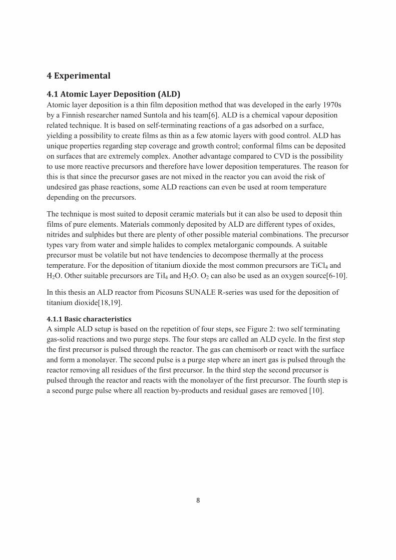
4.1.1 Basic characteristics
A simple ALD setup is based on the repetition of four steps, see Figure 2: two self terminating
gas-solid reactions and two purge steps. The four steps are called an ALD cycle. In the first step
the first precursor is pulsed through the reactor. The gas can chemisorb or react with the surface
and form a monolayer. The second pulse is a purge step where an inert gas is pulsed through the
reactor removing all residues of the first precursor. In the third step the second precursor is
pulsed through the reactor and reacts with the monolayer of the first precursor. The fourth step is
a second purge pulse where all reaction by-products and residual gases are removed [10].
9
Complex multilayer structures can be formed because of the ability to vary the precursors from
cycle to cycle.
Figure 2: ALD reaction cycle

10
For the ALD process to work at optimal efficiency some conditions needs to be fulfilled. These
terms can be summarised in a so called ALD window, see Figure 3. If the temperature is too low
there can be insufficient activation energy or condensation of the precursor limiting the growth.
On the other hand if the temperature is too high the precursor can de-compose or re-evaporate
from the surface and thereby affect the growth rate of the film.
There are two common types of ALD- reactors: flow-through and the open and closed reactor.
The open-closed reactor has a low efficiency but a good control of film growth. An open-closed
reactor is optimal for complex surfaces i.e. substrates with a large surface area compared to size.
The downside of the open-closed reactor is the risk for condensation. The flow-through reactor is
efficient and rapid and most suited for more simple substrates. There are two different varieties
of the flow-through reactor: the cold-wall, where the substrate is heated separately and the hot-
wall where the entire reactor is heated. Today many other varieties of reactors are used with
different types of complements and adaptations[20].
Today there are numerous applications for ALD from microelectronics to catalysts. In this thesis
ALD is used to create thin films of titanium dioxide on cemented carbide cutting tools coated
with Ti(C,N). The technique was chosen because of its capability to make so thin and conformal
films[7,10].
Figure 3: ALD-window

11
4.2 Chemical vapour deposition (CVD)
Chemical vapour deposition is one of the most established film deposition methods today both in
the industry and for research. The technique has numerous applications in many different fields.
In CVD a solid material is grown from a vapour phase. The CVD process has many interesting
properties like good step coverage and high deposition rate compared to ALD. The down side is
that you often need high deposition temperatures[12].
At Seco Tools the CVD methods are divided in to two categories HTCVD (High Temperature
CVD), MTCVD (Moderate Temperature CVD). HTCVD has deposition temperatures above
900˚C and MTCVD has deposition temperatures between 750˚C and 900˚C.
4.2.1 Basic characteristics
The reaction processes of CVD are very complex and have several steps, see Figure 4. First the
precursor gases are carried to the reactor by a main gas flow, step 1, where they react
homogeneously with each other to form secondary precursors, step 2. These precursors are
carried to the surface, step 3, and when they are adsorbed, step 4, they diffuse to an energetically
favourable growth site, step 5. On these sites the precursors react heterogeneously and begin to
form a film, step 6 and 7. Residues from the reactions desorb from the surface and are carried
away by the main gas flow, step 8 and 9 [12].
Figure 4: CVD reaction steps

12
There is a risk that reaction by-products are incorporated in the film. There are several factors
influencing these kinds of contaminations. Optimising the deposition temperature is one way to
minimize the contaminations.
Figure 5: CVD schematic overview of the gas flows
Figure 4 shows a schematic view of the CVD reactor and the
gas flows in it. Different combinations of gases are used in
the depositions of the Ti(C,N) and the aluminium oxide. The
precursors used for the deposition of Ti(C,N) are TiCl4 and
CH3CN, also present are N2 and H2. The general reaction
formula can be described as follows:
TiCl4 + yCH3CN → Ti(C,N) + xHCl
For the deposition of Al2O3 the precursors are AlCl3
prepared in a separate reactor and CO2. Other gases needed
are H2 and HCl. H2S is used as a catalyst. There are a
number of different types of CVD reactors. The one used in
this study is a hot-wall reactor. In a hot-wall reactor the
entire reactor is heated, see Figure 5.
Figure 6: CVD-reactor after removal of the furnace.

13
4.3 Analytical techniques
4.3.1 X-ray diffraction (XRD)
X-ray diffraction is an established analytical technique that uses X-rays interactions with a
material to characterise it. With XRD one can identify crystalline phases and their properties
such as composition, grain size, unit cell parameters and much more. The X-ray interaction
studied is a type of elastic scattering called diffraction occurring in materials having long range
atomic order, meaning the material needs to be at least partly crystalline. Some diffraction in
amorphous materials can occur caused by local order. Diffraction arises when the terms of
Bragg’s law is fulfilled.
nλ = 2dsin(θ)
n is an integer, λ is the wavelength of the incoming radiation, d is the distance between the
atomic planes and θ is the diffraction angle, see Figure 7.
Every crystalline material gives rise to a specific combination of diffracted beams depending on
its symmetry, contents and spacing. The data obtained is often displayed in a diffractogram. X-
ray diffraction is a non-destructive technique for a vast majority of materials.
Two types of XRD film analysis were used in this study, θ-2θ scans and gracing-incidence X-ray
diffraction (GIXRD). With θ-2θ scans information about materials phase content and of its
texture can be obtained. In GIXRD the incoming angle of the X-rays is very small, around 0.5˚.
This type of XRD is suited for analyzing ultrathin films. The small incoming angle makes the X-
rays travel a longer distance through the thin film and the signals from the film is enhanced[11].
Figure 7: XRD
4.3.2 X-ray reflectivity (XRR)
X-ray reflectivity analyses the reflected X-rays and utilities the same type of equipment as XRD.
From an XRR analysis you can obtain properties such as film density and film thickness. XRR
only works with extremely smooth surfaces. It is also a non-destructive technique for most
materials[11].

14
4.3.3 X-ray fluorescence (XRF)
X-ray fluorescence is a non-invasive and fast technique that is often used to determine the
elemental composition of a sample. When irradiated with X-rays an element can emit
characteristic fluorescence. These photons are used to give a qualitative identification of the
elements in the sample and they can also give a quantitative evaluation if compared to a
reference sample [11].
4.3.4 Raman spectroscopy
Light can interact with a material in many different ways, in Raman spectroscopy the inelastic
scattering of an intense monochromatic light beam is used to characterise a sample. The
scattering depends on the fact that some energy from the light is transferred to the vibration
modes in the atoms and molecules. The energy losses are specific for the vibration frequencies of
the sample, which gives a Raman spectrum and with it you can, among other things, identify
your sample. Raman spectroscopy can be used on most non-metallic samples from gases to
solids. The technique is non-destructive to most materials[5,9,11].
4.3.5 Electron spectroscopy for chemical analysis (ESCA)
ESCA or X-ray photoelectron spectroscopy (XPS) is a surface analysis technique that is based on
the photoelectric process. The sample is irradiated with X-rays and the emitted electrons are
analysed. Each element has a unique spectrum. Depending on the bonding in the material and its
composition the spectrum changes, peaks can shift position or/and split, giving unique analysing
opportunities. ESCA can also give quantitative information. The analysed electrons have a short
mean free path through the material making ESCA a surface sensitive technique. If combined
with an ion-sputter removing layer by layer displaying new surfaces, ESCA can give an
extremely detailed analysis of the bulk of a material as well. When the sputter is used the sample
is damaged, otherwise the technique is non destructive. To be able to detect the photoelectrons
vacuum is essential[11].

15
4.3.6 Scanning electron microscopy (SEM)
SEM is a versatile technique that is very common in the industries and research facilities since a
couple of decades. It can generate high resolution images at magnifications far beyond the
capability of light optical microscopes.
The instrument generates a picture by a focused electron beam that is scanned over the surface of
the sample; each scanning point represents a pixel in the created image. When the beam hits the
sample a number of different interactions occur. In SEM the backscattered electrons or the
secondary electrons are usually analysed. The backscattered image gives more chemical
information, the contrast in the image depends among other things on the atomic number of the
elements in the sample. Secondary electron gives better and more comprehensible images of the
surface; it is easier to see topography and it provides a higher resolution.
An SEM is often equipped with an EDS (Energy dispersive X-ray spectrograph) detector that
analyse the X-rays that also arise from the electron beam interactions. With this you gain a good
elemental analysis and some quantitative information.
The analysis usually requires vacuum. Some samples can be damaged by the electron beam but
in general it does not destroy the sample. No sample preparation is needed if the sample is an
electrical conductor. A non-conducting sample is more difficult to study because it becomes
charged by the electron beam[11].

16
4.4 ALD of titanium dioxide
The equipment used to deposit the titanium dioxide films was a hot wall ALD reactor from
Picosun. Different thicknesses were tested to determine how thick the titanium dioxide needed to
be to be able to affect the aluminium oxide. The same settings were used in all the depositions
except for the number of cycles which for the most part controls the thickness of the films. The
pulse schedule was tested on beforehand to obtain suitable parameters. Before the samples were
put in the reactor they were cleaned in ethanol in an ultra-sonic bath for ten minutes and then
dried with nitrogen gas. The deposition temperature was 300˚C.
The precursors that were used to deposit titanium dioxide were TiCl4 and H2O.
Table 1: ALD settings
Three types of CVD coated substrates were used as samples. Sample A and B consists of an
MTCVD Ti(C,N). In sample A the Ti(C,N) is fine-grained, and in Sample B it is coarse grained.
Sample C has a very fine-grained HTCVD Ti(C,N) coating. In all cases the precursors used for
coating were TiCl4, CH3CN, N2, and H2.
4.5 CVD of aluminium oxide
Aluminium oxide was deposited by CVD at Seco Tools. The equipment used was a production
scale IonBond system. Three recipes were tested: SM-o001 and SM-o002 where Al2O3 coatings
with different thicknesses. SM-o003 used an oxidizing step prior to Al2O3 deposition. The
deposition temperature for aluminium oxide was 1000˚C.
For the deposition of Al2O3 the precursors are AlCl3 and CO2. Other gases needed are H2 and
HCl. H2S is used as a catalyst. The reaction can be described by the following coupled reactions:
CO2 + H2 → CO + H2O
2AlCl3 + 3H2O → Al2O3 + 6HCl
Samples Number of cycles
A 5,10,25,50,100,200,300,400
B 5,10,25,50,100,200,300,400
C 5,10,25,50,100,200,300,400
Silicon 100,200,300,400
Precursor Pulse time (s)
TiCl4 0,2
H2O 0,5
Purge (N2) 4
Pulse Schedule 0,2 - 4 - 0,5 - 4
17
4.6 Film characterisation
GIXRD was used to identify the phase content of the titanium dioxide films. To confirm the
result the samples were analysed with Raman spectroscopy. The aluminium oxide films were
analysed with θ-2θ scan (Bragg-Brentano geometry) to find out which phase it contained. To
create good overview and get a better understanding of the films structure the samples were
analysed using SEM. To obtain an insight of what happened during the CVD process an ESCA
was performed on the samples. Sputtering aluminium oxide requires a high acceleration voltage
of the beam and in the experiment the voltage used was 4 kV.
In both ALD and CVD there is a risk that residues from the precursor reactions becomes
incorporated in the film and contaminates it. In this case chlorine is most likely to contaminate
the films. If the chlorine content is higher in the ALD films then in the CVD films the adhesion
deteriorates. By analysing the samples with XRF the amount of chlorine in the films could be
determined.
4.6.1 Film thickness
One of the first obstacles encountered in the experimental procedure was how to determine the
thickness of the titanium dioxide films. The most common and simplest way is to analyse the
film with XRF or XRR, but since the underlying layer also contains titanium that wasn’t
possible.
The solution was to use a combination of XRR and ESCA. Silicon wafers, with a native SiO2,
samples were ALD coated at the same time as Samples A, B, and C for 100, 200, 300, and 400
cycles. The silicon samples were analysed using XRR to determine the film thicknesses.
When the thickness was known the silicon samples were analysed with ESCA. The acceleration
voltage used to sputter the titanium dioxide was 2 kV. From the data obtained the sputter rate for
titanium dioxide was calculated. The cutting tool samples were analysed with the same settings
in the ESCA and with the sputter rate known the film thickness could be calculated.
SEM was also used as an alternative method to determine the film thickness. First and foremost
the thickness of the aluminium oxide and titanium carbonitride films was studied in SEM.
4.1.2 Film adhesion
Good film adhesion is crucial for the survivability of a cutting tool; therefore the aluminium
oxide coated samples were tested by sand blasting. The adhesion was then determined by
studying the resulting damage in a light optical microscope, LOM.

18
5 Results
5.1 XRD characterisation
The GIXRD analysis of the samples with titanium dioxide films thicker than 100 cycles showed
only anatase even though the purple colour of the A sample indicated the presences of Magnéli
phases. No traces of rutile were observed. The titanium dioxide films with fewer than 100 cycles
were difficult to analyse because their peak intensity was too low. The main anatase peak is at 25
degrees the other peaks visible are from the underlying Ti(C,N), see Figure 8.
Figure 8: Diffractograms of TiO2 on sample C (upper curve) and reference sample C.
20 30 40 50 60 70 80
(1,1
,1)
(2,0
,0) (2
,2,0
)
(3,1
,1)
(2,2
,2)
(1,0
,1)
(2,0
,0)

19
The aluminium oxide coated samples were analysed with θ-2θ scans to determine the phase
content of the coatings. The analysis of the samples from the SM-o001 and SM-o002 recipes
showed that a film with α-Al2O3 as the predominant phase had formed on all thicknesses of
titanium dioxide, see Figure 9. The unmarked peaks are from underlying layers.
Figure 9: Diffractogram of α-Al2O3 from SM-o002 on sample C with 400 cycles of TiO2.
20 30 40 50 60 70
(0,1
,2)
(1,0
,4)
(1,1
,0)
(0,0
,6)
(1,1
,3)
(2,0
,2)
(0,2
,4)
(1,1
,6)
(2,1
,1)
(1,2
,2)
(0,1
,8)
(2,1
,4)
(3,0
,0)
(1,2
,5)
(2,0
,8)
(1,0
,10
) (1,1
,9)

20
SM-o003 gave κ-Al2O3 on all samples, see Figure 10.
Figure 10: Diffractograms of α-Al2O3 from SM-o002 (lower curve) and κ- Al2O3 from SM-o003 (upper curve), on
sample C
20 30 40 50 60 70 80
(a 0
,1,2
)
(a 1
,0,4
)
(a 1
,1,0
)
(a 0
,0,6
)(a
1,1
,3)
(a 2
,0,2
)
(a 0
,2,4
)
(a 1
,1,6
)
(a 2
,1,1
)(a
1,2
,2)
(a 0
,1,8
)
(a 2
,1,4
)
(a 3
,0,0
)
(a 1
,2,5
)
(a 2
,0,8
)
(a 1
,0,1
0)
(a 1
,1,9
)
k k
k k k
k
k k
k
k k
k k
k
k k
k
k
k
k
k
k
k k
k
k k
k k
k k

21
5.2 Raman characterisation
The Raman spectrum, Figure 11, confirmed the results from the GIXRD that the films contained
titanium dioxide in the form of anatase on all samples. The characteristic anatase peaks are at
~146 cm-1 and ~238 cm-1[17]. The peak at 238 isn’t visible because the peaks from the
underlying Ti(C,N) is in the same range, Figure 12.
0 200 400 600 800 1000
146,2
Inte
nsi
ty (
a.u
.)
Raman spectrum of TiO2 300 cycles
Raman shift (cm-1)
Figure 11: Raman spectrum for TiO2 300 cycles on sample C
0 200 400 600 800 1000
Raman spectrum of Ti(C,N) referens
Inte
nsi
ty (
a.u
.)
Raman shift (cm-1)
Figure 12: Raman spectrum for Ti(C,N) reference, sample C
22
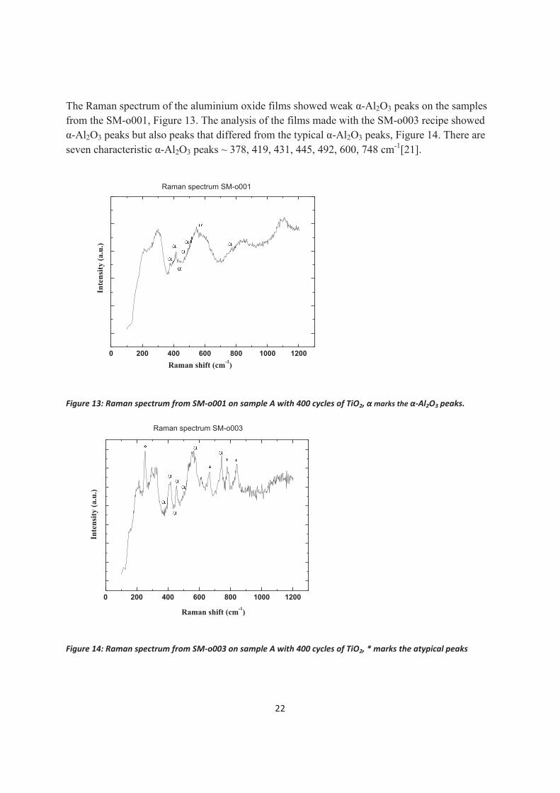
The Raman spectrum of the aluminium oxide films showed weak α-Al2O3 peaks on the samples
from the SM-o001, Figure 13. The analysis of the films made with the SM-o003 recipe showed
α-Al2O3 peaks but also peaks that differed from the typical α-Al2O3 peaks, Figure 14. There are
seven characteristic α-Al2O3 peaks ~ 378, 419, 431, 445, 492, 600, 748 cm-1[21].
0 200 400 600 800 1000 1200
Raman shift (cm-1)
Inte
nsi
ty (
a.u
.)
Raman spectrum SM-o001
Figure 13: Raman spectrum from SM-o001 on sample A with 400 cycles of TiO2, α marks the α-Al2O3 peaks.
0 200 400 600 800 1000 1200
Raman shift (cm-1)
Inte
nsi
ty (
a.u
.)
Raman spectrum SM-o003
Figure 14: Raman spectrum from SM-o003 on sample A with 400 cycles of TiO2, * marks the atypical peaks

23
5.3 ESCA on Al2O3
The ESCA results from after the CVD were inconclusive and it was difficult to determine
whether the film reached was titanium dioxide or titanium carbonitride. The sample displayed in
figure 15 is Sample C with 400 cycles of TiO2 and Al2O3 from the SM-o001 recipe.
Figure 15: ESCA cross-section of the Al2O3 and the transition to the Ti(C,N)
0
10
20
30
40
50
60
70
25 30 35 40 45
Ato
mic
%
Sputter time (min)
Carbon
Nitrogen
Oxygen
Aluminium
Titanium

24
5.4 Evaluation of the film thickness
The silicon samples coated with 200, 300 and 400 cycles were analysed with XRR to determine
the thickness of the titanium dioxide film.
Table 2: XRR and ESCA analysis on TiO2 on silicon
Number of cycles Thickness (nm) Sputter time (min)
200 8 <0,1
300 13 <0,5
400 19 1
From the ESCA analysis of the silicon samples the sputter rate of titanium dioxide was
calculated.
The sputter rate for titanium dioxide was 13-19 nm/min.
The sputter rate was used to calculate the film thickness on the cutting tool samples. The film
thicknesses obtained were rough approximations and the growth rate on the thicker films was
questionable.
Table 3: Thickness of TiO2 on step 9 samples
Number of cycles Thickness (nm) Sputter time (min)
200 13 -19 1
300 39 - 57 3
400 65 - 95 5
Figure 16: ESCA cross-section of the TiO2 film and the transition to the Ti(C,N) on Sample C with 400 cycles of TiO2
0
10
20
30
40
50
60
70
80
90
100
1 2 3 4 5 6 7 8 9 10 11 12
Ato
mic
%
Sputter time (min)
carbon
nitrogen
oxygen
chlorine
titanium

25
5.5 SEM
In the SEM analysis it was impossible to see the titanium dioxide and therefore the film
thickness of it couldn’t be determined by this method. The SEM pictures gave on the other hand
a good overview of the multilayer structure on the samples and the thickness of the aluminium
oxide and the titanium carbonitride could be determined.
Figure17: α-Al2O3 on 400 cycles of TiO2 on Sample C Figure 18: α-Al2O3 on 5 cycles of TiO2 on Sample C
Figure 19: α-Al2O3 with bad adhesion on Sample B Figure 20: κ-Al2O3 from the SM-o003 recipe

26
5.6 XRF
The XRF analysis showed no direct contaminations of chlorine in the films. The chlorine content
was the same before and after the deposition of the titanium dioxide.
5.7 Film adhesion
The adhesion of the aluminium oxide film varied from different film thicknesses of the titanium
dioxide and from different types of samples. Best adhesion had the 5 and 10 cycle thick films on
Sample C.
Figure 21 displays a sample with poor adhesion, the coating is flaking from the sample surface.
Figure 22 displays a sample with good adhesion.
Figure 21: LOM picture of SM-o001 on Sample B
with 400 cycles of TiO2
Figure 22: LOM picture of SM-o001 on Sample C
with 50 cycles of TiO2

27
6 Discussion
The aims of the thesis were achieved; the aluminium oxide films deposited on titanium dioxide
had the desired phase content, α-Al2O3. The thinnest titanium dioxide films gave the best
properties of the α-Al2O3 and good adhesion. On the samples with thicker titanium dioxide films
the adhesion was poor and the SEM analyses on some of the samples showed that the interface
was porous. Sample C had the best adhesion. No increase in the chlorine content was detected.
The deposited titanium dioxide films contained mostly anatase but also some Magnéli phases
which gave Sample A a purple colour. This was interesting in itself, apart from the original aim
of the thesis because new colours are always popular on the market.
After the aluminium oxide was deposited the TiO2 could no longer be detected. The ESCA
probably could have given more answers but the analysis becomes too time-consuming when
thick aluminium oxides films are analysed. To understand what happened with the titanium
dioxide more analyses are required, for example transmission electron microscopy (TEM). One
suggestion is that some of the oxygen in the TiO2 was consumed during the Al2O3 deposition and
Magnéli phases were formed instead. Another proposition is that phases with Ti-Al-O have
formed in the interlayer.
7 Conclusions
α-Al2O3 was successfully deposited on a thin layer of titanium dioxide. Thinner titanium dioxide
films gave better adhesion, thicker films also gave α-Al2O3 but with poor adhesion. Further
research on the subject of what happens to the titanium dioxide during the aluminium oxide
deposition is needed. It would be interesting to investigate even thinner titanium dioxide films to
determine how much is needed. Is only one cycle enough?
If the technique is to be used in industrial scale more research is required on how to adapt the
process.
28
8 Acknowledgements
First and foremost I would like to thank my supervisors Tommy Larsson and Mats Boman for
making this project possible and for their valuable guidance and advises throughout the entire
time. I would also like to thank Oscar Alm for all the good advises and the help at Seco Tools. I
would like to thank Mattis Fondell for teaching me how to handle Picosun, helping me with
many of the analyses and for always answering my more stupid questions.
Thanks to Mikael Ottoson, for reviewing my report and helping me with the XRD analysis.
Special thanks to all my co-workers at the material chemistry department and Seco Tools for
making me feel like home and for all of the fun discussions and memorable moments. David
Rehnlund and Jonas Ångström it would not have been the same without you, thanks for all your
help and support.

29
9 References
1. S. Ruppi, Enhanced performance of α-Al2O3 coatings by control of crystal orientation,
Surface & coatings technology, 2008, vol. 202, 4257-4269.
2. S. Ruppi, Deposition, microstructure and properties of texture-controlled CVD α-
Al2O3coatings, Refractory metals & hard materials, 2005, vol. 23, 306-316.
3. R. M’Saoubi, S. Ruppi, Wear and thermal behaviour of CVD α-Al2O3and MTCVD
Ti(C,N) coatings during machining, CIRP Annals – Manufacturing technology, 2009,
vol. 58, 57-60.
4. A. Larsson, S. Ruppi, Microstructure and properties of Ti(C,N) coatings produced by
MTCVD, Thin Solid Films, 2002, vol. 402, 203-210.
5. I. Dreiling, A. Haug, H. Holzschuh, T. Chassé, Raman spectroscopy as a tool to study
cubic Ti–C–N CVD coatings, Surface & coatings technology, 2009, vol.204, 1008-1012.
6. M. Ritala, M. Leskelä, Surface roughness reduction in atomic layer epitaxy growth of
titanium dioxide thin films, Thin Solid Films, 1994, vol. 249, 155-162.
7. C. Hyun Ko, W. Lee, Formation of Al2O3–TiO2 bilayer using atomic layer deposition and
its application to dynamic random access memory, Solid state electrochem, 2007, vol. 11, 1391-1397.
8. L. Niinistö, M. Leskelä, Atomic layer epitaxy: chemical opportunities and challenges, Thin Solid Films, 1993, vol. 225, 130-135.
9. I. Jõgi, M. Pärs, J. Aarik, A. Aidla, M. Laan, J. Sundqvist, L. Oberbeck, J. Heitmann, K. Kukli, Conformity and structure of titanium dioxide films grown by atomic layer
deposition on silicon substrates, Thin Solid Films, 2008, vol. 516, 4855-4862. 10. R.L. Puurunen, Surface chemistry of atomic layer deposition: A case study for the
trimethylaluminium/water process, Journal of applied physics, 2005, vol. 97. 11. C.R. Brundle, C.A. Evans, S. Wilson, Encyclopedia of materials characterization,
Butterworth-Heinemann, 1992. 12. E. Fredriksson, CVD of titanium dioxides and aluminium oxides, Doctoral thesis, Uppsala
University, 1993. 13. E. Fredriksson, J.-O. Carlsson, Phase transformation during CVD of Al2O3, Journal de
Physique Colloque, 1989, vol. 50, 391-399. 14. E. Fredriksson, J.-O. Carlsson, Factors influencing the κ-Al2O3→α-Al2O3 phase
transformation during CVD, Surface and Coating Technology, 1993, vol. 56, 165-177. 15. E. Fredriksson, J.-O. Carlsson, Chemical vapour deposition of Al2O3 from various gas
mixture, Journal of Chemical Vapour deposition, 1993, vol.1, 333-417. 16. E. Fredriksson, J.-O. Carlsson, Chemical vapour deposition of Al2O3on different titanium
oxides, Journal de Physique, 1995, vol. 73, 38-36. 17. M.Rooth, Metal Oxide Thin Films and Nanostructures Made by ALD, Doctoral Thesis,
Uppsala University, 2008. 18. http://www.picosun.com/files/Picosun_Atomic_Layer_Deposition.pdf, 2010-08-10 19. http://www.picosun.com/products/r_series.php, 2010-08-10 20. http://www.beneq.com/atomic-layer-deposition.html-1, 2011-01-12 21. R. Krishnan, R. Kesavamoorthy, S. Dash, A.K. Tyagi, Baldev Raj, Raman spectroscopic
and photoluminescence investigations on laser surface modified a-Al2O3 coatings, Scripta Materialia, 2003, vol. 48, 1099–1104.