control of high-frequency ac link electronic transformereprints.iisc.ac.in/3402/1/control.pdf ·...
TRANSCRIPT
Control of high-frequency AC link electronictransformer
H. Krishnaswami and V. Ramanarayanan
Abstract: An isolated high-frequency link AC/AC converter is termed an electronic transformer.The electronic transformer has size and cost advantages over a conventional transformer becauseof high-frequency operation of the magnetic core. Of the various topologies of electronictransformer, the high-frequency AC link electronic transformer achieves high-frequency AC powertransformation without a DC link. The circuit uses the standard H-bridge, one on either side of thehigh-frequency transformer. A novel PWM scheme is proposed, which symmetrically delays andadvances the phase of the left and right legs of the front-side converter with respect to the output-side converter. The proposed scheme introduces freewheeling sub-periods, which results in zerovoltage switching in the output-side converter. The electronic transformer as an AC automaticvoltage regulator (AVR) offers distinct advantages over a conventional servo voltage stabiliser interms of size and speed of response. The AVR application is discussed and experimental results of a500VA AVR are presented. A four-quadrant switch presents difficulties in turning off inductiveload current because of the absence of a freewheeling path in the switch. A biasing circuit isproposed to convert the potentially lossy switching transition into lossless transition. Simulationand experimental results with the biasing circuit are presented.
1 Introduction
Line frequency transformers (50 and 60Hz) are heavy andbulky items in power conversion and distribution systems.Transformer size is inversely proportional to the frequencyof operation and saturation flux density. Hence a reductionin volume and weight can be obtained by high-frequencyoperation of the magnetic core. Introduction of a high-frequency link to realise a small-size electronic transformerhas been widely discussed in the literature [1–4]. Low costand easy availability of ferrite core material has helped in theimplementation of high-frequency link power transformation.
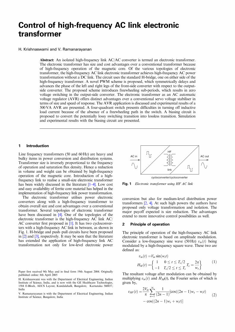
The electronic transformer utilises power electronicconverters along with a high-frequency transformer toobtain overall size and cost advantages over a conventionaltransformer. Several topologies of electronic transformerhave been discussed in [4]. One of the topologies of theelectronic transformer is the high-frequency AC link AC/AC converter first proposed in [1]. It has two cycloconver-ters with a high-frequency AC link in between, as shown inFig. 1. H-bridge and push–pull circuits have been proposedin [2] and [3], respectively. It may be seen that the literaturehas extended the application of high-frequency link ACtransformation not only for low-level electronic power
conversion but also for medium-level distribution powertransformers [2, 4]. At such high powers the authors haveproposed only voltage transformation and isolation. Themajor payoff expected is size reduction. The advantagesextend to more innovative control possibilities as well.
2 Principle of operation
The principle of operation of the high-frequency AC linkelectronic transformer is based on amplitude modulation.Consider a low-frequency sine wave (50Hz) vinðtÞ beingmodulated by a high-frequency square wave. These two aredefined as:
vinðtÞ ¼Vin sinðwitÞ
HMðtÞ ¼1 0 � t � Ts=2
�1 Ts=2 � t � TsTs ¼
2pws
� � ð1Þ
The resultant voltage after modulation can be obtained bymultiplying vinðtÞ and HM(t), the Fourier series of which isgiven by,
vHF ðtÞ ¼2Vin
p
X1n¼1
1
ð2n� 1Þ½cosðð2n� 1Þws � witÞ
� cosðð2n� 1Þws þ witÞ�ð2Þ
AC in AC out
cycloconverter/cycloconverter
HF
link
Fig. 1 Electronic transformer using HF AC link
H. Krishnaswami was with the Department of Electrical Engineering, IndianInstitute of Science, India, and is now with the GE Healthcare Technologies,1584 E-Block, AECS Layout, Kundalahalli, Bangalore, Karnataka 560037,India
V. Ramanarayanan is with the Department of Electrical Engineering, IndianInstitute of Science, Bangalore, India
Paper first received 9th May and in final form 19th August 2004. Originallypublished online: 8th April 2005
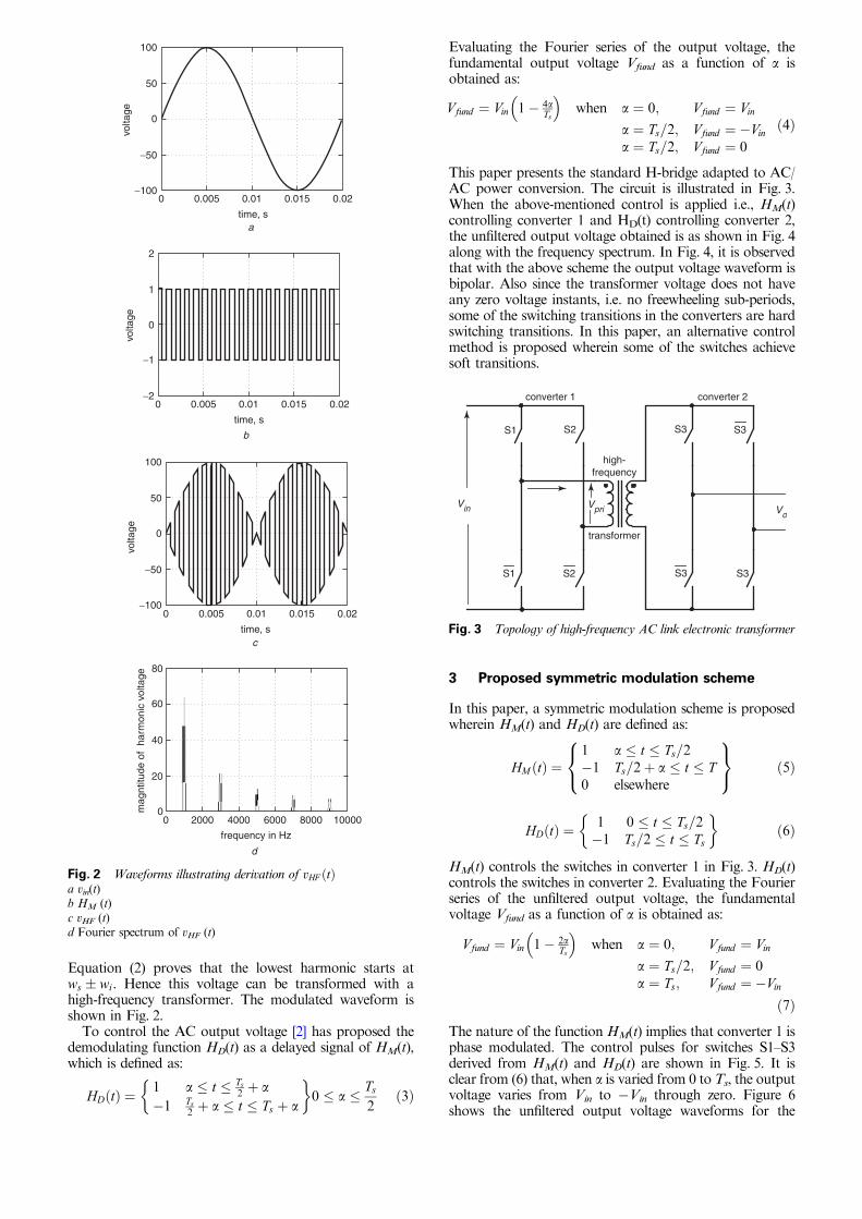
Equation (2) proves that the lowest harmonic starts atws � wi. Hence this voltage can be transformed with ahigh-frequency transformer. The modulated waveform isshown in Fig. 2.
To control the AC output voltage [2] has proposed thedemodulating function HD(t) as a delayed signal of HM(t),which is defined as:
HDðtÞ ¼1 a � t � Ts
2þ a
�1 Ts2þ a � t � Ts þ a
� �0 � a � Ts
2ð3Þ
Evaluating the Fourier series of the output voltage, thefundamental output voltage Vfund as a function of a isobtained as:
Vfund ¼ Vin 1� 4aTs
� �when a ¼ 0; Vfund ¼ Vin
a ¼ Ts=2; Vfund ¼ �Vin
a ¼ Ts=2; Vfund ¼ 0
ð4Þ
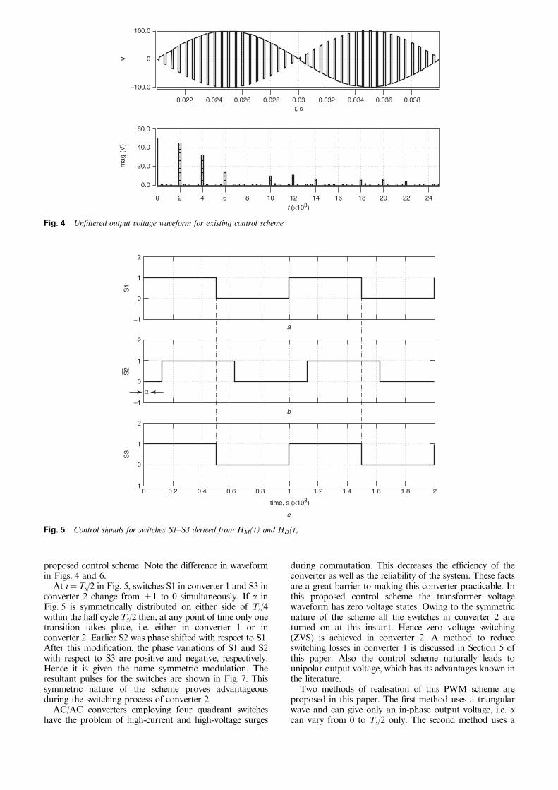
This paper presents the standard H-bridge adapted to AC/AC power conversion. The circuit is illustrated in Fig. 3.When the above-mentioned control is applied i.e., HM(t)controlling converter 1 and HD(t) controlling converter 2,the unfiltered output voltage obtained is as shown in Fig. 4along with the frequency spectrum. In Fig. 4, it is observedthat with the above scheme the output voltage waveform isbipolar. Also since the transformer voltage does not haveany zero voltage instants, i.e. no freewheeling sub-periods,some of the switching transitions in the converters are hardswitching transitions. In this paper, an alternative controlmethod is proposed wherein some of the switches achievesoft transitions.
3 Proposed symmetric modulation scheme
In this paper, a symmetric modulation scheme is proposedwherein HM(t) and HD(t) are defined as:
HM ðtÞ ¼1 a � t � Ts=2�1 Ts=2þ a � t � T0 elsewhere
8<:
9=; ð5Þ
HDðtÞ ¼1 0 � t � Ts=2�1 Ts=2 � t � Ts
� �ð6Þ
HM(t) controls the switches in converter 1 in Fig. 3. HD(t)controls the switches in converter 2. Evaluating the Fourierseries of the unfiltered output voltage, the fundamentalvoltage Vfund as a function of a is obtained as:
Vfund ¼ Vin 1� 2aTs
� �when a ¼ 0; Vfund ¼ Vin
a ¼ Ts=2; Vfund ¼ 0a ¼ Ts; Vfund ¼ �Vin
ð7Þ
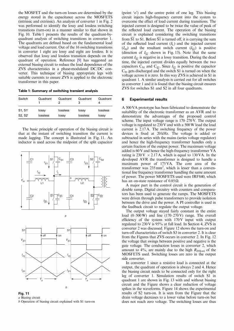
The nature of the function HM(t) implies that converter 1 isphase modulated. The control pulses for switches S1–S3derived from HM(t) and HD(t) are shown in Fig. 5. It isclear from (6) that, when a is varied from 0 to Ts, the outputvoltage varies from Vin to �Vin through zero. Figure 6shows the unfiltered output voltage waveforms for the
100
50
0
−50
−100
volta
ge
0 0.005 0.01 0.015 0.02
atime, s
0 0.005 0.01 0.015 0.02
2
1
0
−1
−2
volta
ge
time, s
b
100
50
0
−50
−100
volta
ge
0 0.005 0.01 0.015 0.02
time, sc
80
60
40
20
00 2000 4000 6000 8000 10000
frequency in Hz
mag
ntitu
de o
f ha
rmon
ic v
olta
ge
d
Fig. 2 Waveforms illustrating derivation of vHF ðtÞa vin(t)b HM (t)c vHF (t)d Fourier spectrum of vHF (t)
S3S2S1
high-frequency
transformer
Vpri
converter 1 converter 2
S1 S2 S3
S3
S3
Vin Vo
Fig. 3 Topology of high-frequency AC link electronic transformer
proposed control scheme. Note the difference in waveformin Figs. 4 and 6.
At t¼Ts/2 in Fig. 5, switches S1 in converter 1 and S3 inconverter 2 change from +1 to 0 simultaneously. If a inFig. 5 is symmetrically distributed on either side of Ts/4within the half cycle Ts/2 then, at any point of time only onetransition takes place, i.e. either in converter 1 or inconverter 2. Earlier S2 was phase shifted with respect to S1.After this modification, the phase variations of S1 and S2with respect to S3 are positive and negative, respectively.Hence it is given the name symmetric modulation. Theresultant pulses for the switches are shown in Fig. 7. Thissymmetric nature of the scheme proves advantageousduring the switching process of converter 2.
AC/AC converters employing four quadrant switcheshave the problem of high-current and high-voltage surges
during commutation. This decreases the efficiency of theconverter as well as the reliability of the system. These factsare a great barrier to making this converter practicable. Inthis proposed control scheme the transformer voltagewaveform has zero voltage states. Owing to the symmetricnature of the scheme all the switches in converter 2 areturned on at this instant. Hence zero voltage switching(ZVS) is achieved in converter 2. A method to reduceswitching losses in converter 1 is discussed in Section 5 ofthis paper. Also the control scheme naturally leads tounipolar output voltage, which has its advantages known inthe literature.
Two methods of realisation of this PWM scheme areproposed in this paper. The first method uses a triangularwave and can give only an in-phase output voltage, i.e. acan vary from 0 to Ts/2 only. The second method uses a
−100.0
0
100.0
0.022 0.024 0.026 0.028 0.03 0.032 0.034 0.036 0.038
60.0
40.0
20.0
0.0
0 2 4 6 8 10 12 14 16 18 20 22 24
Vm
ag (
V)
f (×103)
t, s
Fig. 4 Unfiltered output voltage waveform for existing control scheme
2
1
0
−1
S1
2
1
0
−1
2
1
0
−1
S3
S2
0 0.2 0.4 0.6 0.8 1 1.2 1.4 1.6 1.8 2
time, s (×103)
a
b
c
α
Fig. 5 Control signals for switches S1–S3 derived from HM(t) and HD(t)

double ramp carrier wave to give both in-phase and out-of-phase output voltage. Figs. 8a and b illustrate the twomethods. In Fig. 8b VR is the carrier voltage and VC is thecontrol voltage. VR has two identical ramps shifted by 1801.This method does not introduce a discontinuity at the zerooutput voltage point, i.e. when a¼Ts/2, hence it is useful inclosed-loop control. The second method finds its applica-tion in control of the automatic voltage regulator (AVR),which is explained in the following Section.
4 Application as an automatic voltage regulator
Power-line disturbances such as undervoltage, overvoltage,voltage sags and swells in sensitive equipment such ascomputers, communication services etc., can often lead toloss of valuable data and interruption of communication
services. Traditionally servo voltage stabilisers fill this need.They use a variable autotransformer and an isolationtransformer to inject a compensating voltage in series withthe utility power. Slow dynamic response and bulky linefrequency transformer are the main disadvantages of such asystem. Various methods of providing variable AC havebeen discussed in [5, 6]. But the line frequency magnetics stillform a part of the system. An electronic transformer canreplace the line frequency autotransformer and isolationtransformer by a single high-frequency transformer. Thesize of the system reduces drastically as a result. Such anAVR is shown in Fig. 9. The output voltage of the AVRcan be derived as:
Vo ¼ ð1� nþ 2DnÞ � Vin whereD ¼ aTs
ð8Þ
0.022 0.024 0.026 0.028 0.03 0.032 0.034 0.036 0.038
0 2 4 6 8 10 12 14 16 18 20 22 24
−100.0
0.0
100.0
60.0
40.0
20.0
0.0
Vm
ag (
V)
f (×103)
t, s
Fig. 6 Unfiltered output waveform for proposed control scheme
2
1
0
−1
S1
2
1
0
−1
2
1
0
−1
S3
S2
0 0.2 0.4 0.6 0.8 1 1.2 1.4 1.6 1.8 2
time, s (×103)
a
b
c
�/2
�/2
Fig. 7 Control signals for switches S1–S3 to illustrate symmetric modulation

where Vo is the regulated output voltage of the AVR and nis the transformer turns ratio. Thus when
D ¼ 0; Vo ¼ ð1� nÞVin ðbuckÞD ¼ 0:5; Vo ¼ Vin
D ¼ 1; Vo ¼ ð1þ nÞVin ðboostÞð9Þ
5 Biasing circuit
In this Section a biasing circuit is proposed to reduce theswitching losses of converter 1. Converter 2 switching
transitions are already ZVS, as explained in Section 3.Consider the operation of a single leg in converter 1, asshown in Fig. 2. A capacitive snubber is added across eachswitch to prevent the interruption of load current. Thiscapacitance may be the device capacitance or an externalcapacitance added across the switch. To prevent the sourcegetting short-circuited, a dead time is given between twoswitches in one leg. Figure 10 explains the working of thesingle-leg circuit during the dead time with the transition
from S1 to S1 taken for example. Both positive andnegative input voltages are considered with the current inthe same direction.
Consider initially that S1 is on and the load current is
flowing through S1, as shown in Fig. 10a. When S1 isturned off, the inductive load current splits between the twocapacitors, CS1 and C
S1. The load current is not in the
proper direction to aid the charge transfer from CS1 andC
S1. Instead, the capacitance across switch S1 gets charged
continuously to a value of higher than the bus voltage. BothCS1 and C
S1are charged in the opposite direction, as in
Fig. 10a. When S1 is now turned on, the stored energy getsdissipated in the device. This results in high current spikes.This is a lossy transition. Consider the operation in Fig. 10b.
When S1 is turned off, the reflected load current aids in theenergy transfer between the output capacitance of the two
complementary switches, S1 and S1. When CS1 isdischarged completely to zero, S1 can be turned on. Thisis a lossless transition. A method to prevent overvoltageshas been proposed in [8], which controls each two-quadrantswitch in a four-quadrant switch element. In this paper anovel biasing circuit is proposed to convert the potentiallylossy transitions into lossless transitions.
Turn-on and turn-off losses are the two main constituentsof switching losses. In ZVS converters, the device voltage isbrought to zero just prior to turn-on. During turn-offthe rate of voltage rise is limited, so that the device currentfalls to zero before the voltage rises substantially. Inthe electronic transformer circuit, the turn-off losses arenegligible as a capacitive snubber is added across theswitches. But during turn-on there exists a voltage across
Vc
−Vc
VT
S1, S1
S2, S2
S3
S3
�/2 �/2
Ts
a
b
Vc
−Vc
VR
S1, S1
S2, S2
S3
S3
�/2
Ts
Fig. 8 Control scheme realisationsa Triangular carrierb Double ramp carrier
Vin
S3S2S1
high-frequency
transformer
Vpri
converter 1 converter 2
LC
Vo230V
Va
170V − 270V
S3
S3S2S1 S3
filte
r
Fig. 9 AVR using high-frequency AC link electronic transformer
−
a
+b
S1
S1
Vin Vin
+
+
+−
−
CS1
S1
S1
−
+
−
+
−
I1I1
CS1
CS1 CS1
Fig. 10 Switching transition from S1 to S1 during delay timeshowing direction of current and charging of capacitors CS1 and C
S1
a Lossy transitionb Lossless transition
the MOSFET and the turn-on losses are determined by theenergy stored in the capacitance across the MOSFETS(intrinsic and extrinsic). An analysis of converter 1 in Fig. 2was performed to identify the lossy and lossless switchingtransitions (turn-on) in a manner similar to that shown inFig. 10. Table 1 presents the results of the quadrant-by-quadrant analysis of switching transitions in converter 1.The quadrants are defined based on the fundamental loadvoltage and load current. Out of the 16 switching transitionsin converter 1 eight are lossy and eight are lossless. It isobserved that lossy and lossless transition depends on thequadrant of operation. Reference [9] has suggested anexternal biasing circuit to reduce the load dependence of theZVS characteristics in a phase-modulated DC/DC con-verter. This technique of biasing appropriate legs withsuitable currents to ensure ZVS is applied to the electronictransformer in this paper.
The basic principle of operation of the biasing circuit isthat at the instant of switching transition the current ismade lagging. The concept is illustrated in Fig. 11. Aninductor is used across the midpoint of the split capacitor
(point ‘o’) and the centre point of one leg. This biasingcircuit injects high-frequency current into the system toovercome the effect of load current during transitions. Theinjected current is designed to be twice the value of peak ofthe reflected load current. The operation of the biasingcircuit is explained considering the switching transitions
from S1 to S1. Before S1 is turned off, it is carrying the sumof the reflected load current (IL) and the injected current(Iinj) and the resultant switch current (I
S1) is positive
(direction of IS1
shown in Fig. 13). Note that the samecurrent I
S1is negative in a lossy transition. During the dead
time, the injected current divides equally between the twocapacitors CS1 and C
S1. Since I
S1is positive the capacitor
CS1 gets discharged and the switch S1 is turned on when thevoltage across it is zero. In this way ZVS is achieved in S1 inquadrant 1. A similar analysis is carried out for all switchesin converter 1 and it is found that the biasing circuit ensuresZVS for switches S1 and S2 in all four quadrants.
6 Experimental results
A 500VA prototype has been fabricated to demonstrate thesuitability of the electronic transformer as an AVR and todemonstrate the advantages of the proposed controlscheme. The input voltage range is 170–270V. The outputvoltage is regulated to 230V and with a 500W load the loadcurrent is 2.17A. The switching frequency of the powerdevices is fixed at 20kHz. The voltage is added orsubtracted in series with the mains (series voltage regulator)and hence the high-frequency transformer handles only acertain fraction of the output power. The maximum voltageadded is 60V and hence the high-frequency transformer VArating is 230V � 2.17A, which is equal to 130VA. In thedeveloped AVR the transformer is designed to handle amaximum power of 175VA. The core area of thetransformer was 235mm2, which is lesser than a conven-tional line frequency transformer handling the same amountof power. The power MOSFETS used were IRF840, whichhas an on-state resistance of 0.85O.
A major part in the control circuit is the generation ofdouble ramp. Digital circuitry with counters and compara-tors has been used to generate the ramps. The MOSFETSwere driven through pulse transformers to provide isolationbetween the drive and the power. A PI controller is used inthe feedback circuit to regulate the output voltage.
The output voltage stayed fairly constant in the entireload (0–500W) and line (170–270V) range. The overallefficiency of the system with 170V input with outputregulated to 230V is 95% at full load. In Section 4, ZVS inconverter 2 was discussed. Figure 12 shows the turn-on andturn-off characteristics of switch S3 in converter 2. It is clearfrom the Figures that ZVS occurs in converter 2. In Fig. 12the voltage that swings between positive and negative is thegate voltage. The conduction losses in converter 2, whichamount to 4%, are mainly due to the high RDS(on) of theMOSFETS used. Switching losses are zero in the outputside converter.
In converter 1 since a resistive load is connected at theoutput, the quadrant of operation is always 2 and 4. Hencethe biasing circuit needs to be connected only for the rightleg of converter 1. Simulation results of switch S1 inquadrant 1 are shown in Fig. 13 with and without biasingcircuit and the Figure shows a clear reduction of voltagespikes in the waveforms. Figure 14 shows the experimentalresults of S2 turn-on. It is seen from the Figure that thedrain voltage decreases to a lower value before turn-on butdoes not reach zero voltage. The switching losses are thus
Table 1: Summary of switching transient analysis
Switch Quadrant1
Quadrant2
Quadrant3
Quadrant4
S1, S10 lossy lossless lossy lossless
S2, S20 lossless lossy lossless lossy
Vin o
C1
C2
S1
Iinj
IS1
IL
L1
CS1
o
C3
C4
S2IS3
L2
CS2
S2 CS2
IS2
S1 CS1
IS1
a
off on
S1
off on
Ts Ts
IS1
Iinj
VS1
S1
IS1
Iinj
VS1
b
Fig. 11a Biasing circuitb Operation of biasing circuit explained with S1 turn-on

reduced and the voltage cannot be made zero owing to theabsence of a freewheeling diode across the four-quadrantswitch. This is still advantageous because in a lossytransition the voltage across the switch goes higher thanthe bus voltage. The conduction and switching losses arecalculated for an input voltage of 170V and an outputvoltage of 230V, with the AVR delivering 500W output.The estimated conduction loss in converter 1 was 10W,forming the major loss component, and the switching losseswere negligible. The total measured losses for both theconverters were 25W.
The experimental waveforms of the AVR for theoperating point Vin¼ 170V, Vo¼ 230V and Po¼ 480Ware shown in Figs. 15 and 16. Figure 15 shows the observedprimary voltage and current waveform. The primaryvoltage envelope is not shown for the sake of clarity.Figure 16 shows the observed load voltage and loadcurrent. The waveforms are recorded when the sine voltageis at its maximum and they are shown only for twoswitching cycles. All the waveforms will have 50Hzenvelope, which is not shown in the graphs.
7 Conclusions
The electronic transformer has been introduced and itsprinciple of operation explained. A symmetric modulationscheme for control of electronic transformer is proposed.The advantages of this scheme, such as unipolar outputvoltage waveform and ZVS in the output-side converter, arepresented. An application of the electronic transformer asan AVR is explained in detail. PWM generation methodsfor the control scheme are presented. Experimental resultsof a 500VA AVR are discussed. This paper explains onlyone application but the electronic transformer can also findits use in uninterruptible power supplies wherein theisolation transformer at the output side can be replacedby a high-frequency transformer. Finally a novel biasing
1 100V/ 35.00V/ 0.00s 10.0s/ 244VStop 1
gate voltage
drain voltage
1
Fig. 12 Observed gate and drain voltage waveform of switch S3 inconverter 2 (note ZVS)
200.0
100.0
0.0
−100.0
V
0.005 0.00501
200.0
100.0
0.0
−100.0
V
0.005 0.00501
voltage across switch S1 (Fs = 100 kHz)
voltage across switch S1 with biasing circuit (Fs = 100 kHz)
t, s
t, s
Fig. 13 Simulation results of S1 turn-on with and without biasingcircuit
1 100V/ 35.00V/ 16.1us 200n
s/ 228VStop 1
1
Tdrain voltage gate voltage
Fig. 14 Observed gate and drain voltage waveform of switch S2turn-on
1 100V/ 0.00s 10.0us/ 228VStop 1
1
T
0.00s 10.0su/ 26.6m
vStop 4
4
T
10mv/4
a
b
Fig. 15a Observed transformer primary voltage waveformb Observed transformer primary current waveform

circuit is proposed to convert all lossy transitions inconverter 1 to lossless transitions and the results are alsopresented.
8 References
1 McMurray, W.: ‘Power converter circuits having a high-frequency ink’,US Patent 35173000, 23 June 1970
2 Kang,M., Enjeti, P.N., and Pitel, I.J.: ‘Analysis and design of electronictransformers for electric power distribution system’, IEEE Trans. PowerElectron., 1999, 14, (6), pp. 1133–1141
3 Harada, K., Sakamoto, H., and Shoyama, M.: ‘Phase-controlled DC-AC converter with high-frequency switching’, IEEE Trans. PowerElectron., 1988, 3, pp. 406–411
4 Hienemann, L., and Mauthe, G.: ‘The universal power electronicsbased distribution transformer – an unified approach’. IEEEPESC2001, Conf. Rec.
5 Kwon, B.H., Youm, J.H., and Choi, J.H.: ‘Automatic voltage regulatorwith fast dynamic speed’, IEE Proc. Electr. Power Appl., 1999, 146, (2),pp. 201–207
6 Hietpas, S.M., and Naden, M.: ‘Automatic voltage regulator using anAC voltage-voltage converter’, IEEE Trans. Ind. Appl., 2000, 36,pp. 3–38
7 Hariharan, K.: ‘High frequency AC link electronic transformer’. MScThesis, Department of Electrical Engineering, Indian Institute ofScience, April 2002
8 Enjeti, P.N., and Choi, S.: ‘An approach to realize higher power ACcontroller’. Proc. IEEE APEC Conf., March 1993, pp. 323–327
9 Rajapandian, A., and Ramanarayanan, V.: ‘A Constant FrequencyResonant Transition Converter’, J. Indian Inst. Sci., 1996, pp. 363–37
1 200V/ 0.00s 10.0ms/ 50.0VStop 1
1T
0.00s 10.0sm/ 2.82m
vStop 4
4T
10mv/4
a
b
Fig. 16a Observed output voltage of AVR V0¼ 230Vb Observed load current of AVR IL¼ 2.17AScale: 2A/div