control and protection of multi-der microgrids · control and protection of multi-der microgrids by...
TRANSCRIPT

Control and Protection of Multi-DERMicrogrids
by
Amir Hossein Etemadi
A dissertation submitted in conformity with the requirementsfor the degree of Doctor of Philosophy
Graduate Department of Electrical and Computer EngineeringUniversity of Toronto
Copyright c© 2012 by Amir Hossein Etemadi
Abstract
Control and Protection of Multi-DER Microgrids
Amir Hossein Etemadi
Doctor of Philosophy
Graduate Department of Electrical and Computer Engineering
University of Toronto
2012
This dissertation proposes a power management and control strategy for islanded microgrids,
which consist of multiple electronically-interfaced distributed energy resource (DER) units,
to achieve a prescribed load sharing scheme. This strategy provides i) a power management
system to specify voltage set points based on a classical power flow analysis; 2) DER local
controllers, designed based on a robust, decentralized, servomechanism approach, to track
the set points; and 3) a frequency control and synchronization scheme. This strategy is then
generalized to incorporate both power-controlled and voltage-controlled DER units.
Since the voltage-controlled DER units do not use inner current control loops, they are
vulnerable to overcurrent/overload transients subsequent to system severe disturbances, e.g.,
faults and overloading conditions. To prevent DER unit trip-out or damage under these
conditions, an overcurrent/overload protection scheme is proposed that detects microgrid
abnormal conditions, modifies the terminal voltage of the corresponding VSC to limit DER
unit output current/power within the permissible range, and restores voltage controllers
subsequently.
Under certain circumstances, e.g., microgrid islanding and communication failure, there
is a need to switch from an active to a latent microgrid controller. To minimize the resultant
transients, control transition should be performed smoothly. For the aforementioned two
circumstances, two smooth control transition techniques, based on 1) an observer and 2) an
auxiliary tracking controller, are proposed to achieve a smooth control transition.
A typical microgrid system that adopts the proposed strategy is investigated. The microgrid
dynamics are investigated based on eigenvalue sensitivity and robust analysis studies to
evaluate the performance of the closed-loop linearized microgrid. Extensive case studies,
ii

based on time-domain simulations in the PSCAD/EMTDC platform, are performed to evaluate
performance of the proposed controllers when the microgrid is subject to various disturbances,
e.g., load change, DER abrupt outage, configuration change, faults, and overloading conditions.
Real-time hardware-in-the-loop case studies, using an RTDS system and NI-cRIO industrial
controllers, are also conducted to demonstrate ease of hardware implementation, validate
controller performance, and demonstrate its insensitivity to hardware implementation issues,
e.g., noise, PWM nonidealities, A/D and D/A conversion errors and delays.
iii

Acknowledgements
I owe my deepest gratitude to my thesis supervisor, Professor Reza Iravani, who exemplifies
the virtues of hard work and dedication, whose energy and empathy are limitless, and whose
patience in meticulously proofreading the numerous revisions of my papers continues to amaze
me. His wisdom, insight, and comprehensive approach to the problem have contributed greatly
to this thesis and to my intellectual development. Professor Iravani has provided a role model
that I have aspired to match. I hope this work is only the prelude to an enduring friendship
and future research collaboration.
I am deeply honored by the support of Professor Edward J. Davison who generously agreed
to collaborate in this project and without whose help this dissertation would not have been
possible. His encyclopedic knowledge of controls theory is incredible and the insights I have
acquired through this collaboration will always be with me. My gratitude and thanks also go to
Houshang Karimi for connecting me to Professor Davison and assisting with the early stages of
my dissertation.
I am grateful to my committee members, Professors Olivier Trescases, Zeb Tate, Peter Lehn,
and Vijay Sood for their time, comments, and suggestions. I also thank my fellow graduate
students of Energy Systems Group and colleagues at the Center for Applied Power Electronics
(CAPE) for our useful and insightful discussions. In particular, I thank Afshin Rezaei-Zare,
Milan Graovac, Ali Nabavi-Niaki, Xiaolin Wang, Afshin Pourarya, Ali Mehrizi-Sani, Tim Chang,
Mohamed Kamh, Kayhan Kobravi, and Mahdi Davarpanah.
I also acknowledge the generous financial support I received from the University of Toronto
and Professor Iravani.
I am eternally indebted to my parents for their everlasting support and unconditional love.
Lastly, and most importantly, I would like to thank my life partner and lovely wife, Maryam,
for bringing joy to my life in so many different ways, and for all the sacrifices she has had to
make over the course of my studies. Her patience and understanding has been an inspiration,
and it is with pride and gratification that I dedicate this dissertation to her.
Amir Hossein Etemadi
University of Toronto
August 2012
iv

To Maryam

Contents
Contents vi
List of Tables x
List of Figures xi
Nomenclature xiv
1 Introduction 1
1.1 Background . . . . . . . . . . . . . . . . . . . . . . . . . . . . . . . . . . . . . . . 1
1.2 Literature Review . . . . . . . . . . . . . . . . . . . . . . . . . . . . . . . . . . . . 2
1.3 Statement of the Problem and Research Objectives . . . . . . . . . . . . . . . . . 4
1.4 Methodology . . . . . . . . . . . . . . . . . . . . . . . . . . . . . . . . . . . . . . 6
1.5 Dissertation Layout . . . . . . . . . . . . . . . . . . . . . . . . . . . . . . . . . . . 6
2 Robust Decentralized Microgrid Control 8
2.1 Introduction . . . . . . . . . . . . . . . . . . . . . . . . . . . . . . . . . . . . . . . 8
2.2 Study Microgrid System . . . . . . . . . . . . . . . . . . . . . . . . . . . . . . . . 10
2.3 Power Management and Control Strategy . . . . . . . . . . . . . . . . . . . . . . 11
2.3.1 Power Management System . . . . . . . . . . . . . . . . . . . . . . . . . . 12
2.3.2 Frequency Control and Synchronization . . . . . . . . . . . . . . . . . . . 12
2.3.3 Local Controllers . . . . . . . . . . . . . . . . . . . . . . . . . . . . . . . . 13
2.4 Mathematical Model of the Microgrid . . . . . . . . . . . . . . . . . . . . . . . . 14
2.5 Decentralized Control Strategy . . . . . . . . . . . . . . . . . . . . . . . . . . . . 16
2.5.1 Controller Design Requirements . . . . . . . . . . . . . . . . . . . . . . . 17
2.5.2 Existence Conditions . . . . . . . . . . . . . . . . . . . . . . . . . . . . . . 18
2.5.3 Real Stability Radius Constraint . . . . . . . . . . . . . . . . . . . . . . . 19
vi

2.5.4 Controller Design Procedure . . . . . . . . . . . . . . . . . . . . . . . . . 19
2.5.5 Obtained Decentralized Controller . . . . . . . . . . . . . . . . . . . . . . 21
2.6 Analysis of Microgrid Dynamics . . . . . . . . . . . . . . . . . . . . . . . . . . . 22
2.6.1 Eigenvalues and Participation Factors . . . . . . . . . . . . . . . . . . . . 22
2.6.2 Eigenvalue Sensitivity Analysis . . . . . . . . . . . . . . . . . . . . . . . . 24
2.7 Robustness Properties of the Microgrid . . . . . . . . . . . . . . . . . . . . . . . 26
2.7.1 Robustness of the Nominal Closed-loop System . . . . . . . . . . . . . . 26
2.7.2 Robustness Sensitivity Analysis . . . . . . . . . . . . . . . . . . . . . . . 26
2.7.3 Input and Output Gain-Margins . . . . . . . . . . . . . . . . . . . . . . . 27
2.7.4 Input Time-Delay Tolerance . . . . . . . . . . . . . . . . . . . . . . . . . . 28
2.8 Test Cases . . . . . . . . . . . . . . . . . . . . . . . . . . . . . . . . . . . . . . . . 29
2.8.1 Off-Line Time-Domain Simulation Test Cases . . . . . . . . . . . . . . . . 29
2.8.1.1 Case-1: Load Change . . . . . . . . . . . . . . . . . . . . . . . . 30
2.8.1.2 Case-2: Set Point Tracking and Power Flow Regulation . . . . 32
2.8.1.3 Case-3: Induction Motor Energization . . . . . . . . . . . . . . 33
2.8.1.4 Case-4: Accidental Outage of DER2 . . . . . . . . . . . . . . . . 34
2.8.1.5 Case-5: Change in Microgrid Configuration . . . . . . . . . . . 35
2.8.2 Hardware-in-the-Loop Test Cases . . . . . . . . . . . . . . . . . . . . . . 37
2.8.2.1 Case 6: Sudden Load Increase . . . . . . . . . . . . . . . . . . . 39
2.8.2.2 Case 7: Accidental DER2 Outage . . . . . . . . . . . . . . . . . . 40
2.9 Conclusions . . . . . . . . . . . . . . . . . . . . . . . . . . . . . . . . . . . . . . . 40
3 Overcurrent and Overload Protection 43
3.1 Introduction . . . . . . . . . . . . . . . . . . . . . . . . . . . . . . . . . . . . . . . 43
3.2 Voltage Control Scheme . . . . . . . . . . . . . . . . . . . . . . . . . . . . . . . . 44
3.3 Overcurrent Protection Scheme . . . . . . . . . . . . . . . . . . . . . . . . . . . . 45
3.3.1 Microgrid with a Single VC-DER Unit . . . . . . . . . . . . . . . . . . . . 45
3.3.1.1 Fault Detection . . . . . . . . . . . . . . . . . . . . . . . . . . . . 45
3.3.1.2 Fault Current Limiting Scheme . . . . . . . . . . . . . . . . . . 46
3.3.1.3 Fault Clearance Determination and Controller Restoration . . 46
3.3.2 Microgrid with Multiple VC-DER Units . . . . . . . . . . . . . . . . . . . 47
3.3.2.1 Fault Clearance Determination . . . . . . . . . . . . . . . . . . . 47
3.3.2.2 Voltage Control Restoration . . . . . . . . . . . . . . . . . . . . 48
3.3.3 VC-DER Units with LCL Filters . . . . . . . . . . . . . . . . . . . . . . . . 49
3.4 Overload Protection . . . . . . . . . . . . . . . . . . . . . . . . . . . . . . . . . . . 51
3.5 Performance Evaluation . . . . . . . . . . . . . . . . . . . . . . . . . . . . . . . . 52
vii

3.5.1 Offline Time-domain Simulation Studies . . . . . . . . . . . . . . . . . . 52
3.5.1.1 Case 1: Overcurrent Protection – Temporary Fault . . . . . . . 52
3.5.1.2 Case 2: Overcurrent Protection – Successful Reclosure . . . . . 54
3.5.1.3 Case 3: Overcurrent Protection – Unsuccessful Reclosure . . . 54
3.5.1.4 Case 4: Overload Protection . . . . . . . . . . . . . . . . . . . . 55
3.5.2 Hardware-in-the-loop Simulation Test Case . . . . . . . . . . . . . . . . . 56
3.5.2.1 Case 5: Overcurrent Protection – Temporary Fault . . . . . . . 57
3.6 Conclusions . . . . . . . . . . . . . . . . . . . . . . . . . . . . . . . . . . . . . . . 58
4 Generalized Microgrid Control 60
4.1 Introduction . . . . . . . . . . . . . . . . . . . . . . . . . . . . . . . . . . . . . . . 60
4.2 Study System . . . . . . . . . . . . . . . . . . . . . . . . . . . . . . . . . . . . . . 61
4.3 Power Management and Control Strategy . . . . . . . . . . . . . . . . . . . . . . 62
4.3.1 Power Management System . . . . . . . . . . . . . . . . . . . . . . . . . . 62
4.3.2 Frequency Control and Synchronization . . . . . . . . . . . . . . . . . . . 63
4.3.3 Local Controllers . . . . . . . . . . . . . . . . . . . . . . . . . . . . . . . . 63
4.4 Analysis of Microgrid Dynamics . . . . . . . . . . . . . . . . . . . . . . . . . . . 65
4.4.1 Eigenvalue and Participation Factor Studies . . . . . . . . . . . . . . . . 65
4.4.2 Robustness Analysis . . . . . . . . . . . . . . . . . . . . . . . . . . . . . . 67
4.5 Performance Evaluation . . . . . . . . . . . . . . . . . . . . . . . . . . . . . . . . 68
4.5.1 Offline Time-domain Simulation Studies . . . . . . . . . . . . . . . . . . 69
4.5.1.1 Case 1: Load Change . . . . . . . . . . . . . . . . . . . . . . . . 69
4.5.1.2 Case 2: Load Sharing by the PMS . . . . . . . . . . . . . . . . . 70
4.5.1.3 Case 3: DER2 Overload Protection . . . . . . . . . . . . . . . . . 71
4.5.2 Hardware-in-the-loop Simulation Test Case . . . . . . . . . . . . . . . . . 72
4.5.2.1 Case 4: Induction Motor Energization . . . . . . . . . . . . . . . 72
4.6 Conclusions . . . . . . . . . . . . . . . . . . . . . . . . . . . . . . . . . . . . . . . 73
5 Smooth Microgrid Control Transition 76
5.1 Introduction . . . . . . . . . . . . . . . . . . . . . . . . . . . . . . . . . . . . . . . 76
5.2 Transition to Islanded Mode of Operation . . . . . . . . . . . . . . . . . . . . . . 77
5.2.1 Smooth Transition Scheme Based on a State Observer . . . . . . . . . . . 77
5.2.2 Performance Evaluation . . . . . . . . . . . . . . . . . . . . . . . . . . . . 78
5.2.2.1 Planned Islanding . . . . . . . . . . . . . . . . . . . . . . . . . . 79
5.2.2.2 Unintentional Islanding . . . . . . . . . . . . . . . . . . . . . . . 80
5.3 Control Transfer due to Communication Failure . . . . . . . . . . . . . . . . . . 81
viii

5.3.1 Smooth Transition Based on an Auxiliary Controller . . . . . . . . . . . . 82
5.3.2 Performance Evaluation . . . . . . . . . . . . . . . . . . . . . . . . . . . . 83
5.3.2.1 Simultaneous Transfer to Backup Controller . . . . . . . . . . . 84
5.3.2.2 Nonsimultaneous Transfer to Backup Controllers . . . . . . . . 84
5.4 Conclusions . . . . . . . . . . . . . . . . . . . . . . . . . . . . . . . . . . . . . . . 85
6 Conclusions 87
6.1 Summary & Conclusions . . . . . . . . . . . . . . . . . . . . . . . . . . . . . . . . 87
6.1.1 Qualitative Conclusions . . . . . . . . . . . . . . . . . . . . . . . . . . . . 88
6.1.2 Quantitative Conclusions . . . . . . . . . . . . . . . . . . . . . . . . . . . 89
6.2 Contributions . . . . . . . . . . . . . . . . . . . . . . . . . . . . . . . . . . . . . . 90
6.3 Future Research Directions . . . . . . . . . . . . . . . . . . . . . . . . . . . . . . . 90
A Mathematical Model Details 92
A.1 Equations in abc Frame . . . . . . . . . . . . . . . . . . . . . . . . . . . . . . . . . 92
A.2 Equations in dq Frame . . . . . . . . . . . . . . . . . . . . . . . . . . . . . . . . . 92
A.3 State-space Equations . . . . . . . . . . . . . . . . . . . . . . . . . . . . . . . . . . 93
A.4 Mathematical Model of the Microgrid of Fig. 4.1 . . . . . . . . . . . . . . . . . . 95
B Output Power Control 97
C Droop Control 98
C.1 DER Unit Configuration . . . . . . . . . . . . . . . . . . . . . . . . . . . . . . . . 98
C.2 Frequency Control . . . . . . . . . . . . . . . . . . . . . . . . . . . . . . . . . . . 98
C.3 Voltage Control . . . . . . . . . . . . . . . . . . . . . . . . . . . . . . . . . . . . . 99
References 100
ix

List of Tables
2.1 Parameters of the microgrid . . . . . . . . . . . . . . . . . . . . . . . . . . . . . . 11
2.2 Open-Loop Plant Eigenvalues and Transmission Zeros . . . . . . . . . . . . . . 17
2.3 Eigenvalues of the Closed-loop System (2.16) and the Associated Participating
States . . . . . . . . . . . . . . . . . . . . . . . . . . . . . . . . . . . . . . . . . . . 23
2.4 Microgrid Inaccurate Data . . . . . . . . . . . . . . . . . . . . . . . . . . . . . . . 33
2.5 Numerical Parameters of the Induction Machine. . . . . . . . . . . . . . . . . . . 34
4.1 Microgrid Data, Sbase = 1.6 MVA, Vbase = 13.8 kV . . . . . . . . . . . . . . . . . . 62
4.2 Eigenvalues of the Closed-loop System and the Associated Participating States 67
4.3 Numerical parameters of the induction machines . . . . . . . . . . . . . . . . . . 75
x

List of Figures
2.1 (a) A schematic diagram of the studied microgrid, and (b) a block diagram of the
microgrid power management and control strategy. . . . . . . . . . . . . . . . . 10
2.2 The phase-angle waveform generated by the internal oscillator of DERi. . . . . 13
2.3 Block diagram of the ith local control agent, LCi. . . . . . . . . . . . . . . . . . . 14
2.4 Single-line diagram of the microgrid of Fig. 2.1(a) used to derive state-space
equations. . . . . . . . . . . . . . . . . . . . . . . . . . . . . . . . . . . . . . . . . 14
2.5 Trajectories of eigenpairs (1,2), (3,4), and (5,6) as load inductance and capacitance
increase, (a) Li → αLi, (b) Ci → αCi, 0.1 < α < 10. . . . . . . . . . . . . . . . . . 24
2.6 (a) Trajectories of eigenpairs (7,8) and (9,10) as VSC filter impedance changes
from 0.05 pu to 0.3 pu, (b) trajectories of eigenpairs (7,8), (9,10), and (11,12) as the
controller gain K2 is scaled with a factor of 0.1 < α < 8. . . . . . . . . . . . . . . 25
2.7 Bode plot of the closed-loop system, corresponding to LC1 (associated with input
Vd,re f 1 and output Vd1). . . . . . . . . . . . . . . . . . . . . . . . . . . . . . . . . . 27
2.8 (a) Effect of load parameter perturbations on the robustness of the control scheme,
(b) effect of VSC filter impedance and distribution line length on the closed-loop
system robustness. . . . . . . . . . . . . . . . . . . . . . . . . . . . . . . . . . . . 28
2.9 Effect of the controller gain K2 on the robustness and settling time of the closed-
loop system. . . . . . . . . . . . . . . . . . . . . . . . . . . . . . . . . . . . . . . . 29
2.10 Bode plots of the transfer function Vd1(s)/Vdre f ,1(s) for (a) α = 1, (b) α = 0.5. . . 30
2.11 Increase in real power of Load2 at t = 1 s from 0 to 0.8 pu . . . . . . . . . . . . . 31
2.12 Reference set point tracking and power flow control. . . . . . . . . . . . . . . . . 33
2.13 Induction motor energization . . . . . . . . . . . . . . . . . . . . . . . . . . . . . 35
2.14 DER2 accidental outage. . . . . . . . . . . . . . . . . . . . . . . . . . . . . . . . . 36
2.15 Single-line diagram of the extended microgrid to a loop configuration. . . . . . 36
2.16 Response to microgrid configuration change. . . . . . . . . . . . . . . . . . . . . 37
2.17 Real-time simulation test bed, (a) schematic diagram, and (b) picture. . . . . . . 38
2.18 Microgrid transients due to a load change. . . . . . . . . . . . . . . . . . . . . . . 39
2.19 DER2 unplanned outage, real-time simulation. . . . . . . . . . . . . . . . . . . . 41
xi

3.1 Schematic diagram of a DER unit that controls the voltage at PCC. . . . . . . . 44
3.2 Block diagram of a VC-DER voltage control scheme. . . . . . . . . . . . . . . . . 45
3.3 Dynamic phasors of a VC-DER unit, relating VSC terminal and PCC voltages. . 46
3.4 PCC voltage magnitude during a single-phase to ground fault condition and its
lower envelop. . . . . . . . . . . . . . . . . . . . . . . . . . . . . . . . . . . . . . . 48
3.5 Flowchart of the voltage control scheme including the overcurrent protection. . 50
3.6 Schematic single-line diagram of a DER unit equipped with an LCL filter. . . . . 50
3.7 Three-phase output currents of DER1 during a fault while the overcurrent pro-
tection scheme is disabled. . . . . . . . . . . . . . . . . . . . . . . . . . . . . . . . 52
3.8 Performance of the overcurrent protection scheme for an L-L-L-G fault at PCC1. 53
3.9 Performance of the overcurrent protection scheme for a temporary L-G fault at
the middle of Line1 and its subsequent single-pole successful reclosure. . . . . . 55
3.10 Performance of the overcurrent protection scheme for a permanent L-G fault at
the middle of Line1 . . . . . . . . . . . . . . . . . . . . . . . . . . . . . . . . . . . 56
3.11 Apparent output power of the three DER units when Load1 increases beyond
the maximum generation capacity of DER1. . . . . . . . . . . . . . . . . . . . . . 57
3.12 Three-phase voltages of PCC1 and PCC2 while overload protection scheme in
service. . . . . . . . . . . . . . . . . . . . . . . . . . . . . . . . . . . . . . . . . . . 57
3.13 Power transients subsequent to restoration of LC1 while the anti-windup scheme
is disabled. . . . . . . . . . . . . . . . . . . . . . . . . . . . . . . . . . . . . . . . . 57
3.14 Transients of PCC1 voltages and DER1 output currents due to a L-L-L-G fault at
PCC1. . . . . . . . . . . . . . . . . . . . . . . . . . . . . . . . . . . . . . . . . . . . 58
3.15 Fault detection speed of the proposed overcurrent protection scheme. . . . . . . 58
4.1 (a) A schematic diagram of the studied microgrid system, (b) configuration of
each DER unit. . . . . . . . . . . . . . . . . . . . . . . . . . . . . . . . . . . . . . . 61
4.2 Block diagram of LCi where x and X can represent either voltage or current in
abc and dq frames of reference, respectively. . . . . . . . . . . . . . . . . . . . . . 64
4.3 Trajectories of eigenvalue pairs when controller parameter Ki is scaled by αi
(Arrow shows the increase in the corresponding parameter): (a) 1 < α1 < 160,
(b) 0.1 < α2 < 2, (c) 0.8 < α3 < 1.2, (d) 0.8 < α5 < 1.2. . . . . . . . . . . . . . . . 68
4.4 Effect of the controller parameter K2 on the robustness and settling time of the
closed-loop system. . . . . . . . . . . . . . . . . . . . . . . . . . . . . . . . . . . . 69
4.5 Bode plots of the transfer function Vd1(s)/Vdre f ,1(s) for the control parameter
change: K2 → αK2, (a) α = 1, (b) α = 0.5. . . . . . . . . . . . . . . . . . . . . . . 70
xii

4.6 Microgrid transients due to CB1 opening: (a) PCC2 voltage, (b)–(d) real/reactive
output power of the three DER units, P: Q: . . . . . . . . . . . . . . . . 71
4.7 Achieving a prescribed load sharing scheme by the PMS: (a) PCC2 voltage, (b)–(d)
real/reactive output power of the three DER units, P: Q: . . . . . . . . 72
4.8 Overloading protection: (a) PCC2 voltage, (b)–(d) apparent/real/reactive output
power of the three DER units, P: Q: S: . . . . . . . . . . . . . . . . . 73
4.9 Resolving the overload condition by assigning new power set points for PC-DER
units: (a) PCC2 voltage, (b)–(d) apparent/real/reactive output power of the three
DER units, P: Q: S: . . . . . . . . . . . . . . . . . . . . . . . . . . . . 74
4.10 Microgrid transients due to simultaneous energization of three induction motors. 75
5.1 A block diagram of the voltage control scheme. . . . . . . . . . . . . . . . . . . . 78
5.2 The proposed observer-based smooth transition scheme. . . . . . . . . . . . . . 79
5.3 Planned islanding of the microgrid while the smooth transfer scheme is deacti-
vated/in service. . . . . . . . . . . . . . . . . . . . . . . . . . . . . . . . . . . . . 80
5.4 Unintentional islanding of the microgrid due to a fault in the main grid. . . . . 81
5.5 Smooth control transfer scheme based on an auxiliary tracking controller. . . . 82
5.6 Droop-based backup control scheme that provides smooth transition, L: Latent,
A: Active. . . . . . . . . . . . . . . . . . . . . . . . . . . . . . . . . . . . . . . . . 83
5.7 Transfer to backup control while the smooth transition scheme is deactivated/in
service. . . . . . . . . . . . . . . . . . . . . . . . . . . . . . . . . . . . . . . . . . . 84
5.8 Nonsimultaneous transfer to backup control. . . . . . . . . . . . . . . . . . . . . 85
B.1 (a) Schematic diagram of a DER unit, (b) block diagram of the current control loop. 97
C.1 Schematic diagram a DER unit which is interfaced to the remainder of microgrid
at the PCC. . . . . . . . . . . . . . . . . . . . . . . . . . . . . . . . . . . . . . . . . 98
C.2 Block diagram of the (a) f /P and (b) V/Q droop-based control. . . . . . . . . . 99
xiii

Nomenclature
List of AbbreviationsCB Circuit Breaker
DER Distributed Energy Resource
DFM Decentralized Fixed Mode
DRSP Decentralized Robust Servomechanism Problem
FPGA Field-Programmable Gate Array
GPS Global Positioning System
HIL Hardware-In-the-Loop
IEEE Institute of Electrical and Electronics Engineers
IGBT Insulated Gate Bipolar Transistor
LC Local Controller
LCL Inductive(L)-Capacitive(C)-Inductive(L)
LTI Linear Time-Varying
MIMO Multi-Input Multi-Output
NI-cRIO National Instrument-Compact Reconfigurable Input Output
PC-DER Power-Controlled DER
PCC Point of Common Coupling
PID Proportional, Integral, Derivative
PLL Phase-Locked Loop
PMS Power Management System
PWM Pulse-Width Modulation
RL Resistive(R)-Inductive(L)
RLC Resistive(R)-Inductive(L)-Capacitive(C)
RMS Root Mean Square
RTDS Real-Time Digital Simulator
SISO Single-Input Single-Output
xiv
SPWM Sinusoidal Pulse-Width Modulation
UL Underwriters Laboratories
VC-DER Voltage-Controlled DER
VSC Voltage-Sourced Converter
List of Symbolsα Scaling factor
βi Stabilizing compensator states of ith control agent
X Dynamic phasor corresponding to X
∆Itol Tolerance level for restoring the original controller
∆ Real perturbation matrix
δi Set point for PCCi voltage angle
δik Difference in voltage angle between PCCi and PCCk
ε Controller design parameter
ηi Servo-compensator states of ith control agent
γ Voltage restoration level used for fault clearance determination
Λ Solution of the Lyapunov matrix equation
Cg Left-half complex plain
C1,i, C2,i Controller transfer functions corresponding to Subsystemi
A,B State-space matrices of the stabilizing compensator
Ki Controller gains
ν Number of decentralized control agents
ω0 Nominal power angular frequency
β Input time-delay tolerance
∂Cg Imaginary axis
θ0 Initial phase-angle
θi Phase-angle waveform of DERi
A State matrix of the open-loop system
Ac State matrix of controller
Ao State matrix of observer
Aclose State matrix of the closed-loop system
B Input gain matrix of the open-loop system
Bc Input gain matrix of controller
Bi Input gain matrix of Subsystemi
Bo Input gain matrix of observer
Bik Imaginary part of the element Yik of YBus
xv

C Output gain matrix of the open-loop system
CA Active controller
Cc Output gain matrix of controller
Ci Output gain matrix of Subsystemi
CL Latent controller
ctran Constant coefficient to account for current transients
Dc Feedforward matrix of controller
E Unknown disturbance gain matrix
e Error signal
Ei(s) Error signal of Subsystemi in frequency domain
F Unknown output noise matrix
f0 Nominal power frequency
G Plant
Gik Real part of the element Yik of YBus
I Identity matrix
Imax Maximum permissible output current
Idi,re f Set point for the d-component of DERi current
ii,abc Three-phase output current of DERi
Ii,dq d and q components of output current of DERi
iLi,abc Three-phase current of the reactive branch of Loadi
ILi,dq d and q components of current of the reactive branch of Loadi
Ip f Prefault current
Iqi,re f Set point for the q-component of DERi current
Irs Output current for restoration process
Iti,dq d and q components of current of Linei
Iti,dq d and q components of current of Linei
J Optimal control cost function
M, N Scaling matrices for real stability radius computation
mi Number of outputs of the ith control agent
n Order of the open-loop system
Pi Real power injected at PCCi
PDG,i Real power output of DERi
pki Participation factor relating the ith eigenvalue to the kth state variable
PLoss Total real power loss
Pre f ,i Set point for the output real power of DERi current
Qi Reactive power injected at PCCi
xvi
QDG,i Reactive power output of DERi
QLoss Total reactive power loss
Qre f ,i Set point for the output reactive power of DERi current
Rg Resistance of the main grid Thevenin equivalent
Ri Resistive branch of Loadi
ri Number of outputs of Subsystemi
rR Real stability radius
R f i Resistance of DERi filter
Rli Series resistance of the reactive branch of Loadi
S DER unit output MVA
Sbase Base MVA
Smax DER unit MVA capacity
TL Auxiliary tracking controller
u Controller output
ui Controller output to Subsystemi
Ui(s) Controller output to Subsystemi in frequency domain
Vi Voltage of PCCi
vi, wi Right and left eigenvectors associated with the ith eigenvalue
Vbase,high Base voltage for the high-voltage side of the transformer
Vbase,low Base voltage for the low-voltage side of the transformer
Vd,re f ,i Set point for the d-component of PCCi voltage
Vdc Ideal DC source representing the prime mover
vi,abc Three-phase voltage of PCCi
Vi,dq d and q components of voltage of PCCi
Vq,re f ,i Set point for the d-component of PCCi voltage
vt,abc,i,HV VSCi terminal voltage referred to the high-voltage side
vt,abc,i,LV VSCi terminal voltage referred to the low-voltage side
Vtd,i d-component of the voltage terminal of VSCi
Vtd,mod Modified VSC terminal voltage, d-component
vti,abc Three-phase voltage of VSCi terminal
Vti,dq d and q components of voltage of VSCi terminal
Vtq,i q-component of the voltage terminal of VSCi
Vtq,mod Modified VSC terminal voltage, q-component
x State variable
Xg Reactance of the main grid Thevenin equivalent
XT Transformer leakage reactance
xvii

XCi Capacitive branch of Loadi
X f i Reactance of DERi filter
XLi Reactive branch of Loadi
y Output of the open-loop system
yi Open-loop system output of Subsystemi
Yi(s) Output of Subsystemi in frequency domain
YBus Bus admittance matrix
Yik ikth element of the bus admittance matrix
yobs Observer output
yire f Set points of Subsystemi
xviii

1 Introduction
1.1 Background
TECHNICAL and economical viability of the distributed energy resource (DER) technolo-
gies for distribution voltage class applications have resulted in the rapid deployment of
DER units at distribution voltage classes. This increasing interest is due to the following bene-
fits: local response to load growth, reduction of environmental impacts, low capital investment
and construction time of DER systems, deferral of transmission and distribution expansion,
reduction of distribution and transmission losses, and power quality/reliability enhancement
by generation augmentation. Difficulties arise, however, due to the interconnection of DER
units in the absence of appropriate control and power management, e.g., variation in voltage
profile as well as power flow direction, increase in short circuit level, lack of coordination or
malfunction of the conventional protective devices, instability issues, and potential adverse
impact on reliability and power quality [1].
To fully realize the emerging potential of DER technologies and avoid their drawbacks,
a system approach can be taken which views distributed generation and associated loads
as a microgrid [2–4]. A microgrid is a group of DER units and electrical loads, served by a
distribution system, that acts as a single controllable entity with respect to the main grid. A
microgrid should be able to operate in grid-connected mode, islanded mode, and the transition
between these two [5].
In grid-connected mode, the microgrid voltage and frequency are predominantly dictated by
the main grid. The microgrid control strategy ensures that electrical loads within the microgrid
are supplied by the DER units and the excess (shortage) of power can be managed by exporting
(importing) power to (from) the main grid. In grid-connected mode of operation, DER units are
generally required to generate a constant amount of power with a prespecified range of power
factor, e.g., a power factor greater than 0.95 [6, 7].
1.2 Literature Review 2
In the islanded mode of operation, which was not permitted until the approval of IEEE
Standard 1547.4 [8], the microgrid operates as an autonomous power system and its control
strategy must regulate voltage/frequency of the system and create a balance between microgrid
net demand and generation. Controlling a microgrid, especially in the islanded mode of
operation, is inherently more complicated as compared with a conventional power system
due to the following reasons [9]: close geographical/electrical proximity of DER units that
closely couple; fast dynamics and short response time of DER units, particularly electronically-
coupled units; low energy storage capacity and lack of inertia due to the increasing penetration
and/or dominance of electronically-interfaced DER units; nondispatchable nature of certain
DER technologies such as wind and solar photovoltaic; and the high degree of uncertainty in
microgrid load composition and parameters.
This research work seeks to devise a control strategy that maintains voltage and frequency of
an islanded microgrid that consists of multiple electronically-interfaced DER units and enables
it to ride through transients caused by system disturbances such as load change, DER unit
switching, fault conditions, distribution line outage, and other disturbances.
The rest of this chapter is organized as follows. Section 1.2 reviews the technical literature
concerning the existing microgrid control methods and identifies their merits/drawbacks.
Section 1.3 presents the statement of the problem and research objectives. The proposed
methodology to achieve research objectives is presented in Section 1.4. Section 1.5 provides the
dissertation layout.
1.2 Literature Review
The existing microgrid control schemes can be divided into droop-based and non-droop-
based approaches. Controlling DER units based on droop characteristics is the ubiquitous
method in the literature [10–17]. The droop-based approach originates from the principle of
power balance of synchronous generators in large interconnected power systems. That is, an
imbalance between the input mechanical power of the generator and its output electric real
power causes a change in the rotor speed which is translated to a deviation of the frequency.
Likewise, output reactive power variation results in deviation of voltage magnitude. The same
principle is artificially employed for electronically-interfaced DER units of a microgrid as well.
Opposite droop control, i.e., using real power/voltage and reactive power/frequency droop
characteristics, has also been applied for low voltage microgrids in view of their low X/R
ratios [18, 19].
The main advantage of a droop-based approach is that it obviates the need for communica-
tion since the control action is performed merely based on local measurements. This feature

1.2 Literature Review 3
gives droop control a significant flexibility in that as long as a balance between generation and
demand can be maintained, there is no interdependency between the DER unit local controllers.
However, a droop-based approach inherently exhibits a number of limitations [20–23]:
• It suffers from poor transient performance or instability issues due to the use of average
values of active and reactive power over a cycle.
• It generally does not take into account the load dynamics and consequently, may fail or
not properly respond after a large or a fast load change.
• It cannot initiate a black start and certain provisions are required for system restoration.
• It exhibits poor performance when adopted for distribution networks due to their low
X/R ratios.
• It fails to provide accurate power sharing among the DER units due to output impedance
uncertainties.
• It is not suitable for nonlinear loads since it fails to account for harmonic currents.
• It fails to fully decouple active and reactive power components.
• It fails to provide a fixed frequency and frequency restoration for distribution system is
not a fully resolved issue.
Droop-based methods have been modified in an attempt to overcome these drawbacks by
including a frequency restoration loop [24]; introducing virtual output impedance for more
precise power sharing [21, 25–28]; proposing an adaptive droop function to improve tran-
sient performance [29], including an adaptive feedforward compensation to imrove microgrid
stability [20]; including a VDC/VAC droop characteristics to account for DC-link voltage fluc-
tuations [19]; drooping the inverter output voltage angle rather than its frequency using the
GPS system to achieve a better transient performance [30]; and including an internal controller
to address nonlinearity and imbalance of microgrid loads [31–34]. Small signal stability and
eigenvalue analysis of converter-fed microgrids that are controlled based on droop characteris-
tics are also reported in the literature [26, 35–37] and conclude that the dominant modes of the
closed-loop system are determined by droop controllers, and the overall stability of the system
depends on droop control gains, system loading conditions, and network parameters.
The second category of the existing microgrid control methods in the technical literature are
non-droop-based approaches which can be further divided into schemes that are suitable for (i)
a single-DER and (ii) a multi-DER microgrid. The main objective of the former schemes is to
control the voltage/frequency of the microgrid within a permissible range, whereas the latter
schemes should also provide appropriate load sharing among the DER units. The following
schemes have been proposed for single-DER microgrids: a voltage controller, designed using
an H∞ approach and repetitive control technique, to mitigate voltage harmonics of the point of
common coupling (PCC) [38]; a robust control scheme for a microgrid designed based on an

1.3 Statement of the Problem and Research Objectives 4
H∞ approach to provide a robust performance [39]; and a robust servomechanism approach
for PCC voltage control [40]. These methods are, however, only applicable to single-DER
microgrids.
The reported control schemes for an islanded multi-DER microgrid are as follows. A
centralized controller is proposed in [35] where a central controller determines the contribution
of each DER unit and an outer voltage control loop regulates the voltage of the system. This
method results in fast mitigation of transients; however, it relies on the availability of a voltage-
controlled DER unit and a high-bandwidth communication link. It is suggested in [41] that
a master/slave control strategy be utilized where a dominant DER unit regulates microgrid
voltage and other units supply the load. This method is flexible in terms of connection and
disconnection of DER units, however the presence of the dominant DER is crucial. A voltage
control and power sharing method for multiple parallel DER units in a microgrid is proposed
in [42, 43] where a low-bandwidth communication link is used to achieve load sharing and
voltage is controlled through a central controller. This method is only applicable to a single-bus
microgrid whose DER units operate in parallel.
Although a great deal of research exists on the development of microgrid control strate-
gies, none fully address the following requirements: robustness to topological and parametric
uncertainties, satisfactory transient response of the controllers, obviating the need for a com-
plex communication infrastructure, improving fault ride-through capabilities, and developing
smooth control transition schemes. This research is an attempt to develop a microgrid control
strategy to address the drawbacks/limitations of the existing approaches and meet the above
requirements.
1.3 Statement of the Problem and Research Objectives
As it was presented in the previous section, each of the existing control schemes suffers from
one or more of the following limitations/weaknesses:
• lack of adequate robustness and inability to accommodate microgrid uncertainties,
• poor transient performance,
• inability to initiate a black start after system collapse,
• dependency on specific microgrid configurations,
• coupled real/reactive output power components of DER units,
• relying on a dominant DER unit to regulate microgrid voltage/frequency,
• the need for a high-bandwidth and uneconomical communication link,
• lack of a back-up control scheme in case of communication failure, and
• the need to modify a central controller after each DER unit switching.

1.3 Statement of the Problem and Research Objectives 5
This research work seeks to develop a microgrid control strategy that addresses the limita-
tions of the existing methods with the following objectives:
1. To develop a voltage control method to maintain the stable operation of an islanded
microgrid consisting of electronically-interfaced DER units;
2. To develop a power management system to specify set points for DER local controllers;
3. To generalize the control scheme such that DER units can control either their output
power or the corresponding PCC voltage;
4. To develop an overcurrent/overload protection scheme, as a part of the proposed
controller, to prevent damage and trip-out of DER units due to overcurrent/overload,
subsequent to disturbances, e.g., faults and overloading conditions;
5. To devise a back-up control in case of communication failure and provide smooth
transition from the main to the backup controllers;
6. To provide a smooth control transition scheme in case of microgrid transition from
grid-connected to islanded mode of operation.
To achieve these objectives, an innovative high-performance, MIMO1, robust2, decentral-
ized3 control strategy is proposed. This control scheme is suitable for the problem of controlling
a multi-DER islanded microgrid in view of the following considerations.
• A MIMO controller can inherently account for multiple input/output control channels.
The proposed control strategy is performed in a dq frame of reference, and as a result,
each controller has at least two inputs and outputs that are accounted for through a
MIMO control design.
• A robust control strategy is preferred due to microgrid uncertainties, e.g., load changes,
DER units switchings, and configuration changes. These uncertainties can cause os-
cillations and/or instability due to the lack of enough energy storage and inertia in a
microgrid. However, a robust microgrid controller guarantees a satisfactory performance
despite microgrid unmeasurable disturbances/uncertainties.
• A decentralized control is well suited for a microgrid for the following reasons.
The DER units are not necessarily in geographical proximity. Therefore, employing
local decentralized controllers for each DER unit obviates the need for commu-
nicating time-varying signals to a distant central control system which needs a
1Multi-Input Multi-Output2Robustness means that the control scheme is capable of stabilizing and maintaining viable operation of the
system despite parametric or structural uncertainties, i.e., the parameters of the plant and its configuration canchange in the practical range of variation while controllers perform satisfactorily despite these plant perturbations.
3Decentralized control is a type of control scheme which splits a central controller into several local controllersthat can perform the same control action without communicating with other peer controllers. Decentralizedcontrol is desirable for complex industrial systems with high dimensionality, information structure constraints, anduncertainty.

1.4 Methodology 6
high-bandwidth communication infrastructure.
A decentralized controller can meet its requirements despite unplanned outage or
abrupt connection of other DER units, thus eliminating the interdependency of DER
local controllers.
The computational burden of a high order system, e.g., a microgrid, is overcome by
splitting the system into several subsystems and implementing the controller in a
decentralized manner.
The above considerations conclude that the proposed control strategy is a suitable solution for
the problem of islanded microgrid control.
1.4 Methodology
In order to achieve the aforementioned dissertation objectives, the following methodology is
employed:
Linear model development: In this dissertation, the control scheme is devised based on a
linear state-space model of a microgrid. The equations describing the microgrid are
first derived in natural (abc) reference frame and then transformed to a synchronous
(dq) reference frame based on which the robust decentralized controllers are designed.
MATLAB/Simulink environment is used to verify the derived linear model, design and
analyze the proposed control strategy, and evaluate its robustness.
Time-domain simulation: The linear model of the system is unable to represent certain effects
that exist in the actual system such as harmonics and nonlinearities. To evaluate and vali-
date the performance of the proposed control strategy and to investigate the envisioned
controller behavior under the aforementioned unmodeled effects, a time-domain model
of the system, including the proposed control system, is developed in PSCAD/EMTDC
environment. Dynamic behavior of the system is investigated through time-domain
simulations and the performance of the proposed controller is verified thereby.
Hardware implementation: To demonstrate the feasibility of hardware implementation, and
to validate the performance of the proposed control strategies despite real-world imple-
mentation issues, the controllers are implemented and tested in a real-time hard-ware-in-
the-loop (HIL) simulation environment.
1.5 Dissertation Layout
The rest of this dissertation is organized as follows.

1.5 Dissertation Layout 7
Chapter 2 proposes a power management and control strategy for an islanded three-DER
microgrid. The control objective is to regulate the voltage of DER PCCs to achieve a
prespecified load sharing among the DER units. To this end, a PMS specifies voltage set
points for the PCCs based on a classical power flow. The set points are communicated to
local robust decentralized controllers which are designed using a decentralized, robust,
servomechanisms problem (DRSP) approach, based on a linear mathematical model of the
microgrid. Frequency control and DER synchronization is achieved using DER internal
oscillators which are synchronized based on a time-reference signal received from the
GPS system. Microgrid dynamics are investigated based on eigenvalue and robustness
analysis, and performance of the proposed strategy is evaluated based on both offline
time-domain and HIL simulation test cases.
Chapter 3 proposes an overcurrent and overload protection scheme for DER units which
directly control their PCC voltage and consequently are vulnerable to microgrid severe
disturbances, e.g., faults and overloading conditions. Offline time-domain and HIL
simulations verify the performance of the proposed scheme.
Chapter 4 generalizes the voltage control scheme of Chapter 2 and applies it to a more elaborate
microgrid system. In Chapter 2, each DER unit controls the voltage of its PCC to indirectly
regulate its power output. In Chapter 4, however, the microgrid operator can assign a
number of DER units as voltage-controlled to guarantee an acceptable microgrid voltage
profile, and other units operate as power-controlled to generate specified amounts of
real/reactive power. The assignment scheme depends on microgrid configuration, DER
unit locations, load level, and other possible considerations. Analysis of microgrid
dynamics and offline/HIL simulations demonstrate the desirable performance of the
proposed generalized microgrid control strategy.
Chapter 5 proposes two smooth control transition schemes in the event of 1) microgrid transi-
tion from grid-connected to islanded mode of operation, and 2) communication failure.
These control transitions should be performed smoothly while the resultant microgrid
transients do not cause instability or trigger the protection system. To this end, two
smooth control transition schemes, based on 1) an observer (or state estimator) and 2) an
auxiliary tracking controller are proposed for the above two circumstances, respectively.
Simulation results demonstrate feasibility of these smooth control transition schemes.
Chapter 6 summarizes the contributions of the dissertation, presents its conclusions, and
recommends future research directions.

2 Robust Decentralized
Microgrid Control
2.1 Introduction
THIS chapter presents a power management system (PMS) and a control strategy for an
islanded multi-DER microgrid. Based on the proposed strategy (i) the PMS specifies
voltage set points for each voltage-controlled bus based on a power flow analysis, (ii) local
voltage controllers (LCs) provide tracking of the voltage set points, and (iii) an open-loop
frequency control and synchronization scheme maintains system frequency.
The prominent features of the proposed strategy are the following: (i) The PMS precisely
controls power flow of the system and achieves a prescribed load sharing among the DER
units, (ii) LCs track voltage set points and rapidly reject disturbances, (iii) LCs are highly
robust to parametric, topological, and unmodeled uncertainties of the microgrid, (iv) LCs are
implemented in a decentralized manner; this obviates the need for a high-bandwidth commu-
nication medium to feed system’s information to a central authority and makes it scalable for
larger number of DER units, (v) LCs enable the system to sudden connection/disconnection
of DER units, and (vi) frequency of the system is fixed and cannot deviate due to transients.
The proposed approach requires low-bandwidth communication for both synchronization
and PMS data transmission. However, temporary failure of communication will not lead to
system collapse, provided it recovers within a reasonable period of time, i.e., prior to significant
changes in the microgrid operating point.
Local controllers, which are the main focus in this chapter, are developed based on a
decentralized robust servomechanism approach, i.e., a decentralized controller is devised so
that outputs of the system asymptotically track constant reference inputs independent of (i)
constant disturbances to which the microgrid is subjected, and (ii) variations in the plant
parameters and gains of the control system [44]. The robustness and the decentralized nature
of the controller are highly desirable for a microgrid since
2.1 Introduction 9
• a centralized controller which requires all inputs to be communicated to a control cen-
ter is uneconomical due to the complexity and cost of the required high-bandwidth
communication infrastructure, and
• a robust controller overcomes the uncertainty issues of the microgrid structure/parameters.
In a decentralized scheme, a plant often has a number of control agents. Each control agent
has a number of local control inputs and outputs, and a separate and distinct controller is
applied to each control agent. In particular, there exists a solution to the problem of stabilizing
a plant based on a decentralized control system if and only if the plant has no unstable
decentralized fixed modes (DFM) and certain rank conditions of the plant data hold true [45].
The notion of robustness leads to the problem of constructing a controller for a plant such
that the resultant closed-loop system satisfies a given robustness constraint, e.g., having a
comparable real stability radius for both open-loop and closed-loop systems [46, 47]. This can
be done by a decentralized controller design based on the approach of [44, 48–50], subject to
a robustness constraint. The principles of application of this decentralized control scheme to
conventional power systems is provided in [51–55].
In this chapter, the decentralized control strategy is applied to a microgrid system. To ensure
robust performance of the controller, the decentralized controller optimization is carried out
subject to a robustness constraint. To solve the robust servomechanism problem and to achieve
further improvements in microgrid performance, the normal optimal control performance
index, J =∫ ∞
0 (x′Qx + u′Ru)dτ, which is used for obtaining optimal controllers to reject
impulse disturbances, is replaced with the performance index J =∫ ∞
0 (e′e + εu′u)dτ, where
ε > 0 is a small weighting parameter. The resultant optimal controller obtained is an optimal
servomechanism controller [56]. The microgrid model, existence conditions of the controller,
design procedure, and the properties of the closed-loop system, including eigenvalue sensitivity
and robustness analyses are discussed.
To study different performance aspects of the proposed strategy, it is applied to a three-DER
microgrid and the results, based on both off-line and real-time simulations, are presented. A set
of comprehensive digital time-domain simulation studies, in the PSCAD/EMTDC platform,
validates the desired performance of the proposed PMS/control strategy in response to load
change, set point tracking, nonlinear load (induction motor) energization, and changes in the
microgrid topology. To demonstrate the feasibility of the power management and the control
algorithms for digital implementation and also to evaluate the impact of nonidealities, e.g., noise,
A/D and D/A conversion process, discretization error/delay, and PWM errors, performance of
the control system was also examined in a hardware-in-the-loop (HIL) environment.

2.2 Study Microgrid System 10
(a) (b)
The Microgrid PMS and Control Strategy
Vdc
DER1
jX1 R1
PCC
1
Load1
Vdc
DER2
jX2 R2
PCC
2
Load2
Vdc
DER3
jX3 R3
PCC
3
Load3
jXg Rg
GridCBg
Line1
Line2
Controller
V2
PWM1
LC2
Vre f ,2
GPS Time-reference Signal
Controller
V1
PWM2
LC1
Vre f ,1
Controller
V3
PWM3
LC3
Vre f ,3
PMS
System Status
Figure 2.1: (a) A schematic diagram of the studied microgrid, and (b) a block diagram of the
microgrid power management and control strategy.
2.2 Study Microgrid System
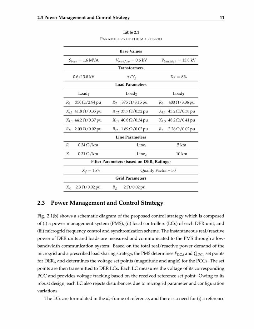
A schematic diagram of a typical radial distribution feeder that is adopted as the study micro-
grid system is illustrated in Fig. 2.1(a). The microgrid includes three dispatchable DER units
with the voltage rating of 0.6 kV and power ratings of 1.6, 1.2, and 0.8 MVA. It also includes
three local loads, and two 13.8-kV distribution line segments. Each DER unit is represented by
a 1.5-kV DC voltage source, a voltage sourced converter (VSC), and a series RL filter. DER units
are interfaced to the grid through a 0.6-kV/13.8-kV step-up transformer (with the same power
rating as the corresponding DER unit) at the point of common coupling (PCC). The main utility
grid is represented by an AC voltage source behind series R and L elements. The microgrid can
be operated in the grid-connected or the islanded modes based on the status of circuit breaker
CBg. The system parameters are given in Table 2.1.
2.3 Power Management and Control Strategy 11
Table 2.1
PARAMETERS OF THE MICROGRID
Base Values
Sbase = 1.6 MVA Vbase,low = 0.6 kV Vbase,high = 13.8 kV
Transformers
0.6/13.8 kV ∆/Yg XT = 8%
Load Parameters
Load1 Load2 Load3
R1 350 Ω/2.94 pu R2 375 Ω/3.15 pu R3 400 Ω/3.36 pu
XL1 41.8 Ω/0.35 pu XL2 37.7 Ω/0.32 pu XL3 45.2 Ω/0.38 pu
XC1 44.2 Ω/0.37 pu XC2 40.8 Ω/0.34 pu XC3 48.2 Ω/0.41 pu
Rl1 2.09 Ω/0.02 pu Rl2 1.89 Ω/0.02 pu Rl3 2.26 Ω/0.02 pu
Line Parameters
R 0.34 Ω/km Line1 5 km
X 0.31 Ω/km Line2 10 km
Filter Parameters (based on DERi Ratings)
X f = 15% Quality Factor = 50
Grid Parameters
Xg 2.3 Ω/0.02 pu Rg 2 Ω/0.02 pu
2.3 Power Management and Control Strategy
Fig. 2.1(b) shows a schematic diagram of the proposed control strategy which is composed
of (i) a power management system (PMS), (ii) local controllers (LCs) of each DER unit, and
(iii) microgrid frequency control and synchronization scheme. The instantaneous real/reactive
power of DER units and loads are measured and communicated to the PMS through a low-
bandwidth communication system. Based on the total real/reactive power demand of the
microgrid and a prescribed load sharing strategy, the PMS determines PDG,i and QDG,i set points
for DERi, and determines the voltage set points (magnitude and angle) for the PCCs. The set
points are then transmitted to DER LCs. Each LC measures the voltage of its corresponding
PCC and provides voltage tracking based on the received reference set point. Owing to its
robust design, each LC also rejects disturbances due to microgrid parameter and configuration
variations.
The LCs are formulated in the dq-frame of reference, and there is a need for (i) a reference
2.3 Power Management and Control Strategy 12
phase-angle for abc(dq) to dq(abc) transformation for each LC, and (ii) a global synchronization
mechanism among all LCs. The reference phase-angle for each LC is generated by the internal
oscillator of each DER unit and the three phase-angle signals are synchronized based on a
common time-reference signal provided by the GPS, Fig. 2.1(b). These entities are further
described in Sections 2.3.1, 2.3.2, and 2.3.3.
2.3.1 Power Management System
The main function of the PMS is to provide load sharing among DER units based on either a
cost function associated with each DER unit or a market signal. After determining the required
real/reactive output power from each DER unit, and measuring the load connected to each
PCC, power flow analysis yields voltage angle δ and magnitude |V| of each PCC. Power flow
equations are
Pi =N
∑k=1|Vi||Vk|(Gik cos δik + Bik sin δik), (2.1)
Qi =N
∑k=1|Vi||Vk|(Gik sin δik + Bik cos δik), (2.2)
where Pi/Qi is the net real/reactive power injected at PCCi, Gik/Bik is the real/imaginary part
of the element Yik of the bus admittance matrix YBus, and δik is the difference in voltage angle
between PCCi and PCCk. Equations (2.1) and (2.2) indicate that power flow of the system is
determined based on the voltage magnitude and angle of PCC1, PCC2, and PCC3. Load and
DER buses measure their power demand and generation and subsequent to a major change,
they notify the PMS to update the set points to maintain an optimal operating point for the
microgrid.
2.3.2 Frequency Control and Synchronization
The microgrid frequency is controlled in an open-loop manner. The LC of DERi includes an
oscillator which generates a 60 Hz sawtooth waveform θi(t) =∫ τ
0 ω0dτ + θ0, where ω0 = 2π f0,
and f0 is the nominal power frequency of the microgrid. Fig. 2.2 illustrates the angle waveform
deduced from the oscillator of LCi which is used for the abc(dq) to dq(abc) transformation of the
DERi mathematical model.
Based on the proposed control strategy, all DER units are synchronized by a global syn-
chronization signal that is communicated to the oscillators of DER units through the GPS [57].
The global synchronization signal is communicated at relatively large time intervals, e.g., one
pulse per second, and is used (i) to prevent drift among local oscillators, and (ii) to initialize
incoming DER units. Crystal oscillators with high accuracies, e.g., an error of 2× 10⁻⁶ to

2.3 Power Management and Control Strategy 13
θi(rad)
t(s)
θ0
2π
One 60 Hz Cycle
Figure 2.2: The phase-angle waveform generated by the internal oscillator of DERi.
2× 10⁻¹¹ seconds per year are currently available at relatively low costs [58]. All LCs can be
synchronized with a high degree of reliability of a common time-reference signal of the GPS
radio clock, e.g., with a theoretical accuracy of 1 µs [59]. Although there are 6–10 satellites
visible to each area at all times, one can rely on the accuracy of crystal oscillators in case of
unavailability of the synchronizing signal.
2.3.3 Local Controllers
The LC of DERi tracks the set points specified by the PMS and rejects disturbances. LCi measures
the voltage of the corresponding PCC, and transforms the three-phase voltage to the dq frame
based on the phase-angle signal θi generated by its internal oscillator and synchronized with
the global time-reference signal received from the GPS. The voltage magnitude and angle set
points received from the PMS, |Vre f ,i|∠δi, are also transformed to the dq frame to generate dq-
based reference values, i.e., Vd,re f ,i = |Vre f ,i| cos δi and Vq,re f ,i = |Vre f ,i| sin δi. The measured and
reference values are provided to LCi to determine the dq voltage components of the terminal of
the corresponding VSC unit, i.e., Vtd,i and Vtq,i, and generate the terminal voltage vt,abc,i,HV at the
high-voltage side of the transformer. vt,abc,i,HV is divided by the turn ratio of the transformer and
shifted if necessary to obtain vt,abc,i,LV corresponding to the low-voltage side of the transformer.
vt,abc,i,LV is then fed to the PWM signal generator of the interface VSC of DERi. It should be
noted that although the realistic and theoretical turn ratio and phase shift of the transformer
are slightly different, the controller can compensate for the mismatch. Fig. 4.2 illustrates a block
diagram of LCi in which the measured and reference voltages are transformed to the dq frame
of reference. After performing the control action, the outputs are transformed to the abc frame
to generate the PWM switching signals of the ith interface VSC.
Section 2.4 develops a mathematical model of the microgrid, based on which the decen-
tralized LCs will be devised in Section 2.5. It should be noted that although the controllers
are designed based on RLC load models, other types of loads, e.g., motor loads, can also be
handled due to the robustness of the controllers.

2.4 Mathematical Model of the Microgrid 14
B∫
K3
A
∫K2
K1
abc/dq
abc/dqTransformer Turn
Ratio and Phase Shift
Compensation
dq/abc
PWM Signal
Generator
VSC of DERi
β
+ +
+
+ +
Vtdq,i
η
+vtabc,i,HV
vtabc,i,LV
+
Vdq,re f ,i−
vabc,i
|Vdq,re f ,i|∠δi
Figure 2.3: Block diagram of the ith local control agent, LCi.
Subsystem1 Subsystem2 Subsystem3
Vt1
R f 1
i1
L f 1
C1
L1
iL1
Rl1
R1
V1 Rt1
it1
Lt1
Vt2
R f 2
i2
L f 2
C2
L2
iL2
Rl2
R2
V2 Rt2
it2
Lt2
Vt3
R f 3
i3
L f 3
C3
L3
iL3
Rl3
R3
V3
Figure 2.4: Single-line diagram of the microgrid of Fig. 2.1(a) used to derive state-space equations.
2.4 Mathematical Model of the Microgrid
The proposed decentralized control is developed based on a linearized model of the microgrid
of Fig. 2.1(a) in a synchronously rotating dq-frame. Fig. 2.4 shows a one-line diagram of the
microgrid model. Each DER unit is represented by a three-phase controlled voltage source and
a series, three-phase RL branch. Dynamics of the source-side of the interface VSC of each DER
unit have secondary effect on the performance of the controller and have not been accounted
for this modeling. Each load is modeled by an equivalent three-phase parallel RLC network.
Each distribution line is represented by lumped, series, three-phase RL elements. The controller
is designed based on the fundamental frequency component of the system of Fig. 2.4.
The microgrid of Fig. 2.4 is virtually partitioned into three subsystems. The mathematical

2.4 Mathematical Model of the Microgrid 15
model of Subsystem1, in the abc frame, isi1,abc = it1,abc + C1
dv1,abcdt + iL1,abc +
v1,abcR1
,
vt1,abc = L f 1di1,abc
dt + R f 1i1,abc + v1,abc,
v1,abc = L1diL1,abc
dt + Rl1iL1,abc,
v1,abc = Lt1dit1,abc
dt + Rt1it1,abc + v2,abc,
(2.3)
where xabc is a 3× 1 vector. The mathematical model associated with other subsystems are pro-
vided in Appendix A. Assuming a three-wire system, (2.3) is transformed to the synchronously
rotating dq-frame of reference, as described in section 2.3.2 by [60]
fdq =23
cos θ cos(θ − 2
3 π) cos(θ − 43 π)
− sin θ − sin(θ − 23 π) − sin(θ − 4
3 π)1√2
1√2
1√2
fabc, (2.4)
where θ(t) is the phase-angle with the frequency of the oscillator internal to DER1. Based on
(2.3) and (2.4), the mathematical model of Subsystem1 in the dq-frame is
dV1,dqdt = 1
C1I1,dq − 1
C1It1,dq − 1
C1IL1,dq − 1
R1C1V1,dq − jωV1,dq,
dI1,dqdt = 1
L f 1Vt1,dq −
R f 1L f 1
I1,dq − 1L f 1
V1,dq − jωI1,dq,dIL1,dq
dt = 1L1
V1,dq − Rl1L1
IL1,dq − jωIL1,dq,dIt1,dq
dt = 1Lt1
V1,dq − Rt1Lt1
It1,dq − 1Lt1
V2,dq − jωIt1,dq.
(2.5)
Similarly, the dq-frame based models of Subsystem2 and Subsystem3, are also developed
(see Appendix A), and used to construct the state-space model of the overall system
x = Ax + Bu,
y = Cx,(2.6)
where
xT =(V1,d, V1,q, I1,d, I1,q, IL1,d, IL1,q, It1,d, It1,q, V2,d, V2,q, I2,d, I2,q, IL2,d, IL2,q, It2,d, It2,q,
V3,d, V3,q, I3,d, I3,q, IL3,d, IL3,q),
uT =(Vt1,d, Vt1,q, Vt2,d, Vt2,q, Vt3,d, Vt3,q
),
yT =(V1,d, V1,q, V2,d, V2,q, V3,d, V3,q
),
and A ⊂ R22×22, B ⊂ R22×6 and C ⊂ R6×22 are the state matrices are given in Appendix A.
The system (2.6) can alternatively be written as
x = Ax + B1u1 + B2u2 + B3u3,
y1 = C1x,
y2 = C2x,
y3 = C3x,
(2.7)

2.5 Decentralized Control Strategy 16
where
yi = (Vi,d, Vi,q), i = 1, 2, 3,
ui = (Vti,d, Vti,q), i = 1, 2, 3,
and a decentralized controller
Ui(s) = C1,i(s)Ei(s) + C2,iYi(s), i = 1, 2, 3, (2.8)
is to be found, where Ei(s) denotes the system error, Ui(s) denotes the input, and the controller
transfer function, C1,i(s),C2,i(s), is restricted to being a proper transfer function, i = 1, 2, 3.
2.5 Decentralized Control Strategy
In this section, the proposed robust decentralized servomechanism controller is designed with
an imposed robustness constraint. To ensure robust performance, the decentralized controller
will be found so that the real stability radius of the final closed-loop system is approximately
the same as that of the open-loop system, i.e., the closed-loop system should have a robustness
index which is not less than 50% of the robustness index of the open-loop system. Throughout
the development, the norm ‖.‖ is assumed to be the spectral norm and a square real matrix
is said to be asymptotically stable if the eigenvalues of the matrix are contained in the open
left-half complex plane.
An extended LTI model of the microgrid based on (2.6) is given by
x = Ax + Bu + Ew,
y = Cx + Fw,
e = y− yre f ,
(2.9)
where x ∈ Rn is the state, u ∈ Rm is the input, y ∈ Rr is the output, ω ∈ RΩ belongs to the
class of unmeasurable constant disturbances, yre f ∈ Rr is the desired constant set point for the
system, and e ∈ Rr is the measured error signal.
The system must contain ν = 3 control agents, each corresponding to one of the three virtual
subsystems of Fig. 2.4, and (2.9) is rewritten as
x = Ax +ν
∑i=1
Biui + Ew,
yi = Cix + Fiw,
ei = yi − yire f ,
(2.10)
where ui and yi are the inputs and outputs of LCi, and ei is the measured error signal, i =
1, 2, · · · , ν. The open-loop eigenvalues and transmission zeros [61] of (2.9), corresponding to

2.5 Decentralized Control Strategy 17
Table 2.2
OPEN-LOOP PLANT EIGENVALUES AND TRANSMISSION ZEROS
Eigenvalues Transmission Zeros
-570.79 ± 4074.8i -1116.71 ± 377.0i
-570.79 ± 3320.8i -1127.93 ± 377.0i
-547.12 ± 2519.7i -18.85 ± 377.0i
-547.12 ± 1765.7i -18.85 ± 377.0i
-29.33 ± 946.1i -18.85 ± 377.0i
-29.33 ± 192.1i
-84.85 ± 377.0i
-39.85 ± 377.0i
-14.07 ± 377.0i
-12.66 ± 377.0i
-11.98 ± 377.0i
the system of Fig. 2.4, are given in Table 2.2, which indicates that the open-loop system is stable
and minimum phase.
2.5.1 Controller Design Requirements
A decentralized controller for the plant (2.10) should provide the following features:
1. The closed-loop system is asymptotically stable.
2. Steady-state asymptotic tracking and disturbance regulation occurs for (i) all constant set
points y1re f , y2
re f , y3re f , and (ii) all constant disturbances w, i.e., limt→∞ ei(t) = 0, i = 1, 2, 3,
for all constant disturbances and set points.
3. The controller is robust, i.e., Condition 2 should hold for practical perturbations of
the plant model (2.10), including dynamic perturbations which do not destabilize the
perturbed closed-loop system.
4. The controller should be “fast” with smooth non-peaking transients, e.g., it should
respond to constant set points and constant disturbance changes, e.g., within about three
cycles of 60 Hz.
5. Low interaction should occur among the output channels of the ν control agents, and
among the outputs contained in each of the ν control agents, for both tracking and
regulation [62].

2.5 Decentralized Control Strategy 18
6. It is required that the above conditions be satisfied for as wide as possible range of the
parameters R, L, C of each load.
These conditions will be achieved by a decentralized controller based on the solution of the
decentralized robust servomechanism problem (DRSP) [44, 48].
2.5.2 Existence Conditions
The following existence conditions for a solution to the DRSP, such that the above conditions
1–3 hold, are obtained from [44]. Given plant (2.10), let
Cm := [C∗T1 , C∗T2 , · · · , C∗Tν ]T, (2.11)
where C∗1 :=[
C1 0 0 ··· 00 Ir1 0 ··· 0
], C∗2 :=
[C2 0 0 ··· 00 0 Ir2 ··· 0
], · · · , C∗ν :=
[Cν 0 0 ··· 00 0 0 ··· Irν
], and let B :=
[B1, B2, · · · , Bν], and C := [CT1 , CT
2 , · · · , CTν ]
T.
Theorem 1 [44]: Given the system (2.10), there exists a solution to DRSP such that conditions
1–3 all hold, if and only if the following conditions are all satisfied:
1. The system (2.10) has no unstable DFM.
2. mi ≥ ri, where mi is the number of outputs of the ith control agent and ri is the number of
outputs of Subsystemi, i = 1, 2, · · · , ν.
3. The system
Cm,[
A 0C 0
], B
has no DFM = 0.
Remark 1: If mi = ri, i = 1, 2, · · · , ν, Condition 3 becomes
rank
[A B
C 0
]= n + r1 + r2 + · · ·+ rν.
For the microgrid of Fig. 2.4, it can be verified that the existence conditions of Theorem
1 are all satisfied. In particular, 1) plant (2.10) has no decentralized fixed modes, 2) it has
mi = ri = 2, i = 1, 2, 3, and 3) the rank of the matrix[
A BC 0
], given by (2.6), is equal to
n + r1 + r2 + r3 = 22 + 2 + 2 + 2 = 28.
Remark 2: In the plant model (2.9), the three load parameters R, L, C of each subsystem,
Fig. 2.4, can vary and result in structural uncertainty in the plant’s nominal model. It is also
observed in (2.9) that the load parameters affect neither the output gain matrix C, nor the input
control matrix B. Therefore, only the A matrix of (2.9) is affected by changing load parameters.
We use this observation to design a controller with the desirable robustness properties.
Remark 3: The following analysis shows that Condition 3 of Theorem 1 always holds true
for the studied microgrid system regardless of its numerical values. The determinant of the

2.5 Decentralized Control Strategy 19
matrix[
A BC 0
]is given by ρ1
ρ2where
ρ1 =(
R2l1 + ω2L2
1) (
R2l2 + ω2L2
2) (
R2l3 + ω2L2
3) (
R2t1 + ω2L2
t1) (
R2t2 + ω2L2
t2)
,
ρ2 =(C1L1L f 1Lt1C2L2L f 2Lt2C3L3L f 3
)2 .
Clearly, the determinant is always non-zero which implies rank[
A BC 0
]= 28 for any numerical
value of microgrid parameters and thus the third condition of Theorem 1 always holds.
2.5.3 Real Stability Radius Constraint
To evaluate the robustness of a control scheme, the following definition is used [47].
Given a real n× n matrix A which is asymptotically stable, assume that A is subject to a real
perturbation A → A + M∆N, where M ∈ Rn×m and N ∈ Rp×n are known scaling matrices
defining the structure and scale of the perturbation [63], and ∆ is a real matrix of uncertain
parameters. Then it is desired to find rstab > 0, such that (i) A + M∆N is asymptotically
stable for all real perturbations ∆ with the property that ‖∆‖ < rstab and (ii) there exists a
perturbation ∆∗ with the property that ||∆∗|| = rstab, such that A + M∆∗N is unstable. In this
case, rstab is called the real stability radius of A, M, N.Real stability radius is the solution of the following linear algebra optimization problem [47]:
rR(A, M, N) =
sup
s∈∂Cg
µR
(N(sI − A)−1M
)−1
, (2.12)
where Cg is the open left-half complex plain, ∂Cg denotes the boundary of Cg, which is the
imaginary axis for continuous-time systems, and
µR(Q) = infγ∈(0,1]
σ2
((ReQ −γImQ
γ−1ImQ ReQ
)), (2.13)
where ReQ and ImQ denote, respectively, the real and imaginary parts of a complex matrix Q,
and σ2(P) denotes the second largest singular value of the real matrix P.
2.5.4 Controller Design Procedure
Given the plant (2.10) with ν = 3, to solve the DRSP it is necessary [44] that the decentralized
controller include the decentralized servo-compensator
ηi = 0ηi + (yi − yire f ), i = 1, 2, 3, (2.14)
where ηi ∈ R2, i = 1, 2, 3, together with a decentralized stabilizing compensator which will be
assumed to have the structure
β = Aβ +By, (2.15)
u = K1y +K2η +K3β,

2.5 Decentralized Control Strategy 20
where
A =
A1 0 0
0 A2 0
0 0 A3
,B =
B1 0 0
0 B2 0
0 0 B3
,K1 =
K1
1 0 0
0 K21 0
0 0 K31
,K2 =
K1
2 0 0
0 K22 0
0 0 K32
,
K3 =
K1
3 0 0
0 K23 0
0 0 K33
,
so that the controlled closed-loop system is described by
x
η
β
=
A + BK1C BK2 BK3
C 0 0
BC 0 A
x
η
β
+
0
−I
0
yre f +
BK1F + E
F
BF
w,
y =[C 0 0
]x
η
β
+ Fw.
(2.16)
In this case, the controller parameters (2.15) are obtained by applying optimal controller design
method [64], [65] to minimize the expected value of the performance index∫ ∞
0 (e′e + εu′u)dτ
given by
J = trace(Γ), (2.17)
where Γ > 0 is obtained by solving the Lyapunov matrix equation corresponding to
∫ ∞
0(e′e + εu′u)dτ =
x(0)
e(0)
β(0)
′
Γ
x(0)
e(0)
β(0)
, (2.18)
where ε = 10−6, subject to the conditions that
1. the resultant closed-loop system (2.16) is asymptotically stable,
2. the real stability radius of the closed-loop system, rR
(Aclose,
[A00
], [I, 0, 0]
)should be
greater than or equal to half of the real stability radius of the open-loop system, rR(A, A, I),
where
Aclose =
A + BK1C BK2 BK3
C 0 0
BC 0 A
.

2.5 Decentralized Control Strategy 21
Substituting for e and u from (2.16) in (2.18) provides a closed-form expression for (2.18)
ATcloseΓ + ΓAclose = −
([0 I 0
]′ [0 I 0
]+ εK∗TK∗
), (2.19)
where K∗ = [K1C,K2,K3]. The control design problem becomes, therefore, a constrained
parameter optimization problem [66] whose solution yields the control parameters A, B, K1,
K2, and K3.
The reason to impose the robust constraint above is that the load parameters Ri, Li, Ci, i =
1, 2, 3 may vary, but since they affect only the A matrix and not the B1, B2, B3, C1, C2, and C3
matrices of (2.10), then it is desired to minimize the effect of load parameter perturbations by
keeping the closed-loop system robustness index, as measured by the real stability radius, as
“close” as possible to the open-loop robustness index. The constraint imposed is such that the
closed-loop robustness index is not less than half of the open-loop robustness index.
2.5.5 Obtained Decentralized Controller
On carrying out the optimization of the controller (2.15) as measured by the performance index
(2.17), the following decentralized controller is obtained for the microgrid of Fig. 2.4:
η = y− yre f ,
β = Aβ +By,
u = K1y +K2η +K3β,
(2.20)
where
u =
u1
u2
u3
, y =
y1
y2
y3
,
K1 =
−15.83 3.37 0 0 0 0
−7.97 −110.14 0 0 0 0
0 0 −5.11 104.77 0 0
0 0 −10.38 −132.44 0 0
0 0 0 0 −5.51 6.81
0 0 0 0 −15.39−118.91
,K2 =
−1047 649 0 0 0 0
−834 −1103 0 0 0 0
0 0 −496 970 0 0
0 0 −1072 −839 0 0
0 0 0 0 −636 793
0 0 0 0 −1002−1039
,
K3 =
0.18 0 0
881.47 0 0
0 −3668.6 0
0 4495.3 0
0 0 −1639.3
0 0 57906
,B =
1 579.02 0 0 0 0
0 0 1 205.21 0 0
0 0 0 0 1 12.754
,

2.6 Analysis of Microgrid Dynamics 22
A =
−5313.5 0 0
0 −7702.2 0
0 0 −6913.2
.
A transfer function representation of the control agents of the decentralized controller (4.3)is given by(
U1(s)
U2(s)
)=
1s
[−1047 649.5
−834.4 −1103.3
](E1(s)
E2(s)
)+
1s + 5313
[−15.83s−8.4× 10⁴ 3.37s + 1.8× 10⁴
−7.97s− 4.1× 10⁴ −110.1s− 7.5× 10⁴
](Y1(s)
Y2(s)
),
(U3(s)
U4(s)
)=
1s
[−495.6 969.7
−1072 −838.6
](E3(s)
E4(s)
)+
1s + 7702
[−5.11s− 4.3× 10⁴ 104.8s + 5.4× 10⁴
−10.38s− 7.5× 10⁴ −132.4s− 9.8× 10⁴
](Y3(s)
Y4(s)
),
(U5(s)
U6(s)
)=
1s
[−635.9 793
−1002 −1039
](E5(s)
E6(s)
)+
1s + 6913
[−5.51s− 4.0× 10⁴ 6.8s + 2.6× 10⁴
−15.39s− 4.9× 10⁴ −118.9s− 8.3× 10⁴
](Y5(s)
Y6(s)
),
where Ui(s), Ei(s), Yi(s), i = 1, 2, · · · , 6, are the outputs and errors of controllers, and plant’s
outputs, respectively. Poles of the decentralized controller are 0 (repeated 6 times), -7702, -6913,
and -5313.
2.6 Analysis of Microgrid Dynamics
To investigate the dynamic behavior of the studied microgrid, eigen analysis including eigen-
value calculation, participation factor analysis, and a set of eigenvalue sensitivity analyses are
carried out and results are presented in this section.
2.6.1 Eigenvalues and Participation Factors
The eigenvalues of the closed-loop system, or alternatively, the eigenvalues of the matrix
Aclose ∈ R31×31 are listed in Table 4.2. Table 4.2 shows that the closed-loop system (2.16) has
14 pairs of complex conjugate and 3 real eigenvalues. Dominant eigenvalues, i.e., eigenvalues
1–8, are highly damped, which indicates the proper design of the controllers. To identify the
dominant eigenvalues, i.e., the closest eigenvalues to the imaginary axis, the eigenvalues are
sorted by their real-part absolute value in an ascending order. To identify the state variables
that dominantly influence an eigenvalue, the normalized participation factors associated with
each eigenvalue are calculated using [67]
pki =vikwki
∑nk=1 vikwki
, (2.21)
where vi and wi are the right and left eigenvectors associated with the ith eigenvalue, and pki
is the participation factor relating the ith eigenvalue to the kth state variable. State variables
include 22 open-loop state variables given in (2.6) and 9 state variables that correspond to the
three LCs. LCi has three states, two of which, ηi ∈ R2 in Table 4.2, participate in regulating the
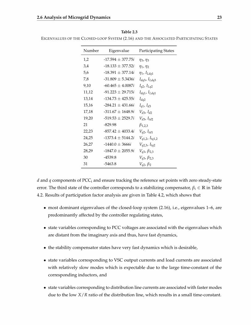
2.6 Analysis of Microgrid Dynamics 23
Table 2.3
EIGENVALUES OF THE CLOSED-LOOP SYSTEM (2.16) AND THE ASSOCIATED PARTICIPATING STATES
Number Eigenvalue Participating States
1,2 -17.594 ± 377.75i η3, η3
3,4 -18.133 ± 377.52i η1, η2
5,6 -18.391 ± 377.14i η1, ILdq1
7,8 -31.809 ± 5.3436i Idq3, ILdq3
9,10 -60.465 ± 4.0087i Iq2, ILq2
11,12 -91.223 ± 29.715i Idq1, ILdq1
13,14 -134.73 ± 425.55i Idq2
15,16 -284.21 ± 431.66i Iq1, Id3
17,18 -311.67 ± 1648.9i Vd3, Id2
19,20 -519.53 ± 2529.7i Vd3, Itd2
21 -829.98 β1,2,3
22,23 -857.42 ± 4033.4i Vq2, Itd1
24,25 -1373.4 ± 5144.2i Vq1,2, Itq1,2
26,27 -1440.0 ± 3666i Vq2,3, Itq2
28,29 -1847.0 ± 2055.9i Vq3, β2,3
30 -4539.8 Vq3, β2,3
31 -5463.8 Vq2, β2
d and q components of PCCi and ensure tracking the reference set points with zero steady-state
error. The third state of the controller corresponds to a stabilizing compensator, βi ∈ R in Table
4.2. Results of participation factor analysis are given in Table 4.2, which shows that
• most dominant eigenvalues of the closed-loop system (2.16), i.e., eigenvalues 1–6, are
predominantly affected by the controller regulating states,
• state variables corresponding to PCC voltages are associated with the eigenvalues which
are distant from the imaginary axis and thus, have fast dynamics,
• the stability compensator states have very fast dynamics which is desirable,
• state variables corresponding to VSC output currents and load currents are associated
with relatively slow modes which is expectable due to the large time-constant of the
corresponding inductors, and
• state variables corresponding to distribution line currents are associated with faster modes
due to the low X/R ratio of the distribution line, which results in a small time-constant.
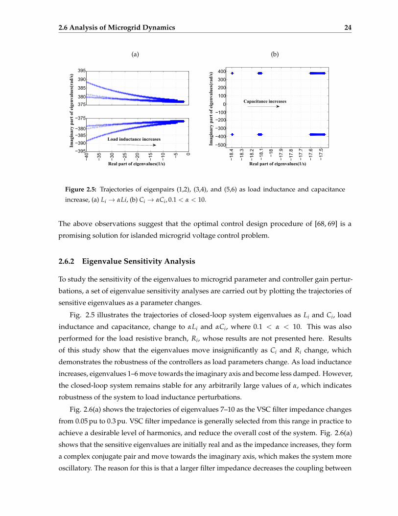
2.6 Analysis of Microgrid Dynamics 24
(a) (b)
375
380
385
390
395
−40
−35
−30
−25
−20
−15
−10 −5 0
−395
−390
−385
−380
−375
Real part of eigenvalues(1/s)
Imag
inar
y p
art
of e
igen
valu
es(r
ad/s
)
Load inductance increases
−18.4
−18.3
−18.2
−18.1
−18
−17.9
−17.8
−17.7
−17.6
−17.5
−500
−400
−300
−200
−100
0
100
200
300
400
Real part of eigenvalues(1/s)
Imag
inar
y p
art
of e
igen
valu
es(r
ad/s
)
Capacitance increases
Figure 2.5: Trajectories of eigenpairs (1,2), (3,4), and (5,6) as load inductance and capacitance
increase, (a) Li → αLi, (b) Ci → αCi, 0.1 < α < 10.
The above observations suggest that the optimal control design procedure of [68, 69] is a
promising solution for islanded microgrid voltage control problem.
2.6.2 Eigenvalue Sensitivity Analysis
To study the sensitivity of the eigenvalues to microgrid parameter and controller gain pertur-
bations, a set of eigenvalue sensitivity analyses are carried out by plotting the trajectories of
sensitive eigenvalues as a parameter changes.
Fig. 2.5 illustrates the trajectories of closed-loop system eigenvalues as Li and Ci, load
inductance and capacitance, change to αLi and αCi, where 0.1 < α < 10. This was also
performed for the load resistive branch, Ri, whose results are not presented here. Results
of this study show that the eigenvalues move insignificantly as Ci and Ri change, which
demonstrates the robustness of the controllers as load parameters change. As load inductance
increases, eigenvalues 1–6 move towards the imaginary axis and become less damped. However,
the closed-loop system remains stable for any arbitrarily large values of α, which indicates
robustness of the system to load inductance perturbations.
Fig. 2.6(a) shows the trajectories of eigenvalues 7–10 as the VSC filter impedance changes
from 0.05 pu to 0.3 pu. VSC filter impedance is generally selected from this range in practice to
achieve a desirable level of harmonics, and reduce the overall cost of the system. Fig. 2.6(a)
shows that the sensitive eigenvalues are initially real and as the impedance increases, they form
a complex conjugate pair and move towards the imaginary axis, which makes the system more
oscillatory. The reason for this is that a larger filter impedance decreases the coupling between
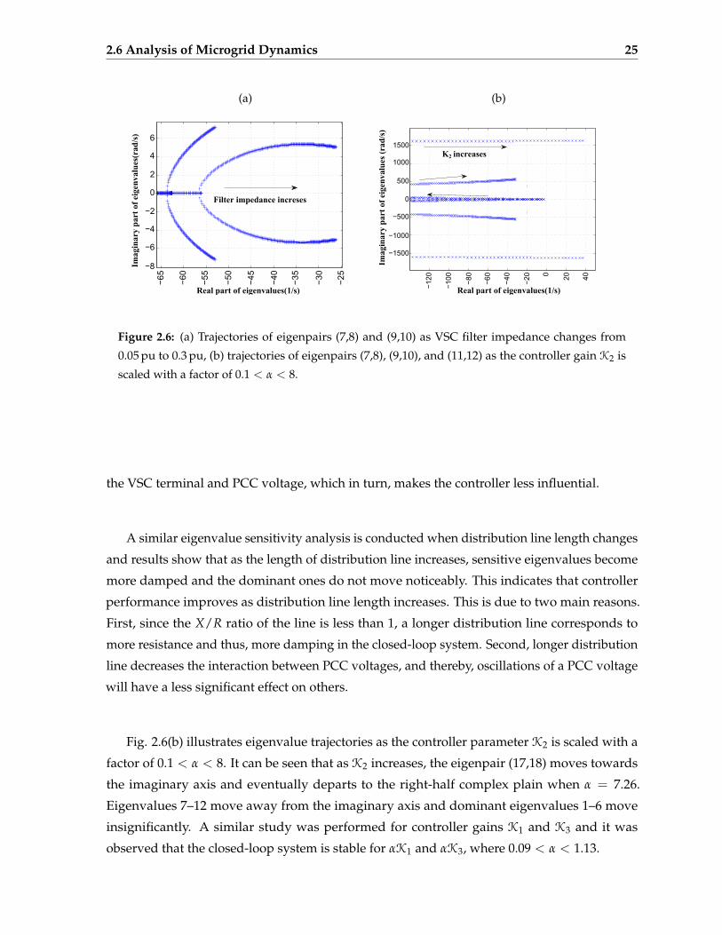
2.6 Analysis of Microgrid Dynamics 25
(a) (b)
−65
−60
−55
−50
−45
−40
−35
−30
−25
−8
−6
−4
−2
0
2
4
6
Real part of eigenvalues(1/s)
Imag
inar
y p
art
of e
igen
valu
es(r
ad/s
)
Filter impedance increses
−120
−100
−80
−60
−40
−20
0 20 40
−1500
−1000
−500
0
500
1000
1500
Real part of eigenvalues(1/s)
Imag
inar
y p
art
of e
igen
valu
es (
rad
/s)
K2 increases
Figure 2.6: (a) Trajectories of eigenpairs (7,8) and (9,10) as VSC filter impedance changes from
0.05 pu to 0.3 pu, (b) trajectories of eigenpairs (7,8), (9,10), and (11,12) as the controller gain K2 is
scaled with a factor of 0.1 < α < 8.
the VSC terminal and PCC voltage, which in turn, makes the controller less influential.
A similar eigenvalue sensitivity analysis is conducted when distribution line length changes
and results show that as the length of distribution line increases, sensitive eigenvalues become
more damped and the dominant ones do not move noticeably. This indicates that controller
performance improves as distribution line length increases. This is due to two main reasons.
First, since the X/R ratio of the line is less than 1, a longer distribution line corresponds to
more resistance and thus, more damping in the closed-loop system. Second, longer distribution
line decreases the interaction between PCC voltages, and thereby, oscillations of a PCC voltage
will have a less significant effect on others.
Fig. 2.6(b) illustrates eigenvalue trajectories as the controller parameter K2 is scaled with a
factor of 0.1 < α < 8. It can be seen that as K2 increases, the eigenpair (17,18) moves towards
the imaginary axis and eventually departs to the right-half complex plain when α = 7.26.
Eigenvalues 7–12 move away from the imaginary axis and dominant eigenvalues 1–6 move
insignificantly. A similar study was performed for controller gains K1 and K3 and it was
observed that the closed-loop system is stable for αK1 and αK3, where 0.09 < α < 1.13.

2.7 Robustness Properties of the Microgrid 26
2.7 Robustness Properties of the Microgrid
2.7.1 Robustness of the Nominal Closed-loop System
The closed-loop system of plant (2.10) and controller (4.3) is highly robust with respect to
changes in the load parameters Ri, Li, Ci, i = 1, 2, 3, of the microgrid. In particular assume
that in the open-loop system (2.9), the matrix A is subject to uncertainty, e.g., due to changes
in the load parameters and perturbations in the elements of the matrix A. Also assume
that A → A(I + ∆) where ∆ is an unknown real perturbation matrix, and where A is an
asymptotically stable matrix. The largest perturbations ∆ for which the system remains stable
is determined from the real stability radius of A.
The open-loop perturbed plant x = A(I + ∆)x remains asymptotically stable for all real ∆
matrix perturbations with ‖∆‖ < rstab if and only if rstab < rstab∗, where rstab∗ = 1.495×10⁻³.
Consider now the closed-loop system obtained by applying the controller (4.3) to (2.10), and
assume that the elements of the controller are fixed and that the Bi and Ci, i = 1, 2, 3, matrices
of the plant are fixed, but that due to load changes in Ri, Li, Ci (and other perturbations) the
elements of A are allowed to perturb. We also assume in the closed-loop plant (2.16) that
A→ A(I + ∆), where ∆ is an unknown perturbation matrix. The perturbed closed-loop system
remains asymptotically stable for all real ∆ matrix perturbations with ‖∆‖ < rstab, if and only
if rstab < rstab∗, where rstab∗ = 7.752× 10⁻².
Thus the stability robustness index of the closed-loop system rstab∗ = 7.752 × 10⁻²
with respect to perturbations of the A matrix is larger than the open-loop system given by
rstab∗ = 1.495× 10⁻³, and so there is no deterioration in robustness of the closed-loop system
as compared to the open-loop system with respect to perturbations of the elements of A. A
bode plot of the closed-loop system is illustrated in Fig. 2.7, which shows that the closed-loop
transfer function from Vd,re f 1 to Vd1 of LC1 has a gain margin of 29.5 dB at the frequency of
372 Hz (as denoted by a dotted line) and a phase margin of -180 which clearly highlights the
robust stability of the closed-loop system.
2.7.2 Robustness Sensitivity Analysis
In this section, the effect of microgrid parameter and controller gain perturbations on the
real stability radius, rR, of the closed-loop system is investigated. To reflect microgrid load
uncertainties, the matrix triple Aclose, [A, A, 0]T, [I, 0, 0] is considered as the argument of the
function rR(.).
Fig. 2.8(a) illustrates variations of rR when each of the parameters Ri, Li, and Ci are scaled

2.7 Robustness Properties of the Microgrid 27
0
-40
-80
-120Mag
nitu
de(d
B)
GM=29.5 dB (at 2340 rad/sec), PM=−180 deg (at 0 rad/sec)
10−1 100 101 102 103 104 105
0
-90
-180
-270
Frequency(rad/sec)
Phas
e(de
g)
Figure 2.7: Bode plot of the closed-loop system, corresponding to LC1 (associated with input Vd,re f 1
and output Vd1).
by a coefficient of 0.5 < α < 2. rR increases as load resistance increases and it decreases as load
inductance and capacitance increase. The reason for this is that more resistance corresponds to
more damping and more inductance and capacitance correspond to more oscillations.
Fig. 2.8(b) illustrates variations of rR as the VSC filter impedance and the length of distribu-
tion feeder change with a coefficient of 0.2 < α < 1.6. It is observed that larger VSC impedances
degrade the robustness of the closed-loop system and a longer distribution feeder will improve
the robustness. Similar results were obtained through eigenvalue sensitivity analysis of Section
2.6.2.
Fig. 2.9 illustrates variations of rR and closed-loop system maximum settling time as the
controller gain K2 changes with a coefficient of 0.1 < α < 1. It can be seen that the increase of
K2 degrades closed-loop system robustness. However, it reduces the maximum settling time
of the system, which corresponds to a faster control performance. Thus, there is a trade-off
between the speed and robustness of the controller. To verify this observation, the bode plots of
the transfer function Vd1(s)/Vdre f ,1(s) are depicted in Fig. 4.5 for two coefficients of α = 1 and
α = 0.5. The gain margin corresponding to a smaller controller gain is larger, which signifies
more robustness, and verifies the conclusion of Fig. 2.9.
2.7.3 Input and Output Gain-Margins
The following definition is an extension of the classical SISO gain-margin to multivariable
systems [70].

2.7 Robustness Properties of the Microgrid 28
(a) (b)
0.5 1 1.5 2
736
738
·10−3
α
r R
L increasesR increasesC increases
0.5 1
755
760
·10−3
α
r R,f
ilt
400
600
800
·10−3
r R,li
ne
rR, f iltrR,line
Figure 2.8: (a) Effect of load parameter perturbations on the robustness of the control scheme, (b)
effect of VSC filter impedance and distribution line length on the closed-loop system robustness.
Definition: Given a plant x = Ax + Bu, y = Cx controlled by a controller η = Acη + Bcy, u =
Ccη, assume that the closed-loop system is asymptotically stable. Let y = Cx be replaced by
y = (I + Ky)Cx, where Ky is a constant gain matrix; then if the closed-loop system remains
stable ∀Ky with ||Ky|| < ly, the system has an output gain-margin of (1 + ly). Also let Bu be
replaced by B(I + Ku)u; then if the closed-loop system remains stable ∀Ku with ||Ku|| < lu, the
system is said to have an input gain margin of (1 + lu). The gain margin can be calculated from
the real stability radius of the system. The closed-loop system (2.10), (4.3) has output and input
gain-margins of 1.38 and 1.28, respectively, which are quite satisfactory [71].
2.7.4 Input Time-Delay Tolerance
Often a system may have time delays which are ignored in its model, and it is important that
the controlled system be robust to such unmodelled effects. The following definition is used to
describe such a robust property [72].
Definition: Given a plant x = Ax + Bu, y = Cx controlled by the controller η = Acη +
Bcy, u = Ccη, assume that the closed-loop system is asymptotically stable, and let u(t) be
replaced by u(t− β), corresponding to a time delay of β s. Then if there exists β > 0 such that
the closed-loop system remains stable ∀β ∈ [0, β], the closed-loop system has an input time-delay
tolerance of β. In this case the closed-loop system (2.10), (4.3) has an input time-delay tolerance
of 1.58× 10⁻⁴ s. This is a lower bound time-delay tolerance and the actual system may be able
to longer delays.

2.8 Test Cases 29
0.2 0.4 0.6 0.8 1
2
4
6
α
Sett
ling
Tim
e(s
)
757
758
759
760
761
·10−3
r R
Settling TimerR
Figure 2.9: Effect of the controller gain K2 on the robustness and settling time of the closed-loop
system.
2.8 Test Cases
A set of test cases, based on both off-line and real-time simulations, are carried out to evaluate
performance of the microgrid of Fig. 2.1(a), in an islanded condition, based on the proposed
control strategy and power management system.
2.8.1 Off-Line Time-Domain Simulation Test Cases
A comprehensive set of test cases, based on digital time-domain simulation studies in the
PSCAD/EMTDC environment, are carried out to evaluate the control performance subject to (i)
a significant load change, (ii) control set point change, (iii) induction motor energization, (iv)
accidental DER outage, and (v) changes in the microgrid topology. The component models for
the test cases are as follows and parameter values are given in Table 2.1:
• Each DER unit is represented by (i) a constant DC voltage source, (ii) a two-level, IGBT-
based VSC, and (iii) a three-phase series filter. The VSC uses a SPWM technique at the
frequency of 6 kHz. The VSC filter is modeled as a series, three-phase RL branch.
• The interface transformer for each DER unit is represented as a linear, three-phase, ∆/Yg
configuration.
• Each three-phase load is represented by a parallel RLC branch at each phase.

2.8 Test Cases 30
0
-40
-80
-120Mag
nitu
de(d
B)
(a)
GM=29.5 dB
0
-40
-80
-120Mag
nitu
de(d
B)
(b)
GM=35.3 dB
100 102 104
0
-90
-180
-270
Frequency(rad/sec)
Phas
e(de
g)
100 102 104
0
-90
-180
-270
Frequency(rad/sec)
Phas
e(de
g)Figure 2.10: Bode plots of the transfer function Vd1(s)/Vdre f ,1(s) for (a) α = 1, (b) α = 0.5.
• Each distribution line section, between two consecutive buses, is modeled by a lumped,
three-phase, series RL branch.
• The analog control system of each DER unit, Fig. 4.2, is discretized with a sampling rate of
6 kHz. The discretized control system is coded in FORTRAN and imbedded as a module
in the PSCAD/EMTDC.
2.8.1.1 Case-1: Load Change
The objective of this case study is to demonstrate robust performance of the LCs subject to
parametric uncertainties of the microgrid. In this case study, the uncertain parameter is the
resistive branch of Load2, given by R2 in Fig. 2.4. Prior to t = 1 s, the R2 branch is open and at
t = 1 s, R2 = 1.61 pu is connected to the system. This change in the value of R2 corresponds
to an increase in the real power demand of Load2 from zero to 0.8 pu, which is equal to the
full generation capacity of DER2. Fig. 2.11 shows the impact of this load change on the system
voltages, power flow, and the modulation index of DER2.
Prior to the load change, the voltages of the three buses are regulated at the prespecified
values of 1∠0. DER2 is under no-load condition at a modulation index of 0.66. Fig. 2.11(a)–(e)
illustrates the d and q components, RMS value, phase-angle, and instantaneous voltages of
PCC2 and indicates the robustness of the LCs in response to transients after the load change.
The microgrid control effectively controls the voltage within 15 ms. Fig. 2.11(e) shows that the
transients of the PCC2 instantaneous voltages are practically insignificant.

2.8 Test Cases 31
0.98
1
1.02
Vd,
2(pu)
(a)
−0.02
0
0.02
Vq,
2(pu)
(b)
0.98
1
1.02
Vrm
s,2(p
u)
(c)
−0.5
0
0.5
VP
h,2(d
eg)
(d)
−1
0
1
Vab
c,2(p
u)
(e)
−0.20
0.20.40.6
PD
G,i(p
u)
(f)
PDG,1
PDG,2
PDG,3
−0.2
0
0.2
QD
G,i(p
u)
(g)
QDG,1
QDG,2
QDG,3
−0.1
0
0.1
PLi
ne,i(p
u)
(h)
PLine,1
PLine,2
0.95 1 1.05 1.1 1.15 1.20.46
0.48
0.5
Time(s)
m2
(i)
0.95 1 1.05 1.1 1.15 1.2Time(s)
Figure 2.11: Increase in real power of Load2 at t = 1 s from 0 to 0.8 pu: (a) and (b) d and q compo-
nents of PCC2 voltage, (c) and (d) RMS value and phase-angle of PCC2 voltage, (e) instantaneous
voltages of PCC2, (f) output real power of the DER units, (g) output reactive power of the DER units,
(h) real power transfer of the distribution lines, (i) modulation index of the VSC of DER2.
Fig. 2.11(f) and (g) depict output real and reactive power components of the three DER units.
Output real power of DER1 and DER3 remain the same as the predisturbance values after riding
through the load-change transients. However, the output real power of DER2 increases from 0
to 0.8 pu in response to the increased power demand of Load2. The real power transferred on
the distribution lines are depicted in Fig. 2.11(h). Since each DER unit supplies its dedicated
load prior to the change of Load2, and since the change is within the supply range of DER2, the
disturbance does not change the steady-state power flow.
Fig. 2.11(i) illustrates the modulation index, m2, of the interface converter of DER2 which
changes from 0.66 to 0.69. The reason for modulation index rise is that the output current of
DER2 increases due to the load increase, and as a result, the voltage drop on the filter impedance
increases. The controller increases the modulation index of DER2 to compensate for the voltage
drop on the filter impedance.
This case study demonstrates the robust performance of the LCs in maintaining the stability
and operational integrity of the system despite the significant parametric perturbation of the
nominal plant. It also indicates fast response of the controllers in regulating PCC2 voltage. The
instantaneous voltages of PCC2 exhibit no observable transients despite the considerable load

2.8 Test Cases 32
increase.
2.8.1.2 Case-2: Set Point Tracking and Power Flow Regulation
The objective of this case study is to demonstrate the capability of LCs in voltage set point
tracking, and as a result, their power flow regulation capability. The adopted load sharing
scheme requires that each DER unit contribute to the net microgrid load, proportional to its
maximum generation capacity, and supply reactive power locally, i.e.,
PDER,i =SMax
DER,i
∑i SMaxDER,i
∑i
PLoad,i,
where SMaxDER,i denotes the maximum apparent power generation capacity of DERi. This case
study follows the previous scenario in which the output real power of DER2 increases in
response to the change in Load2. To share the total power demand among the three DER units,
based on the aforementioned strategy, the PMS assigns the following new set point for the
three LCs, respectively: 1.01∠0.14, 1.00∠0, and 1.00∠− 0.06. At t = 1.5 s, LCs receive the
new set points for tracking. Fig. 2.12 shows transients of the microgrid due to this set point
update. Fig. 2.12(a)–(d) shows the d and q components, RMS value, and phase-angle of PCC1
voltage, and illustrates that LC2 manages to reach the new set points in less than 50 ms with
zero steady-state error. Fig. 2.12(e) shows the instantaneous voltages of PCC1. The output real
and reactive power of the three DER units are illustrated in Fig. 2.12(f) and (g). Prior to t = 1.5 s,
DER2 generates more real power than the other two DER units. After t = 1.5 s, however, the
total real power demand is divided among the DER units proportional to their rated generation
capacities and DER units keep their output reactive power component unchanged. Fig. 2.12(h)
shows real power flows of Line1 and Line2, and indicates changes from zero to 0.25 pu and
0.06 pu, respectively, which are contributions of DER2 and DER3 to the nonlocal load, Load2.
This case study shows the capability of the LCs in tracking the voltage set points specified
by the PMS. It also concludes that power flow can be effectively controlled by specifying
appropriate voltage set points for LCs.
To evaluate performance of the controllers when the PMS specifies set points based on
inaccurate microgrid data, the power flow analysis is performed based on the inaccurate set
of data given in Table 2.4. The results of this study show the microgrid stable operation is
maintained despite the incorrect power flow results. However, the prescribed load sharing has
an error of ±10%.

2.8 Test Cases 33
0.99
1
1.01
Vd,1(pu)
(a)
−0.01
0
0.01
Vq,1(pu)
(b)
0.98
1
1.02
Vrms,1(pu)
(c)
0
0.1
0.2
Vph,1(deg)
(d)
−1
0
1
Vabc,1(pu)
(e)
0
0.5
1
PDG,i(pu)
(f)
PDG,1
PDG,2
PDG,3
−0.2
0
0.2
QDG,i(pu)
(g)
QDG,1
QDG,2
QDG,3
1.4 1.45 1.5 1.55 1.6 1.65 1.7−0.5
0
0.5
PLine,i(pu)
(h)
PLine,1
PLine,2
Time(s)1.4 1.45 1.5 1.55 1.6 1.65 1.7Time(s)
Figure 2.12: Reference set point tracking and power flow control: (a) and (b) d and q components of
PCC1 voltage, (c) and (d) RMS value and phase-angle of PCC1 voltage, (e) instantaneous voltages
of PCC1, (f) output real power of three DER units, (g) output reactive power of the DER units, (h)
real power flow of the distribution lines.
Table 2.4
MICROGRID INACCURATE DATA
Accurate Data Inaccurate Data
Net Load S = 1.68 + j0.33 pu S = 1.51 + j0.3 pu
Line Length Line1=5 km Line1=3 km
Line Length Line2=10 km Line2=14 km
2.8.1.3 Case-3: Induction Motor Energization
The objective of this case study is to illustrate the robust performance of the LCs when the
microgrid is subject to a nonlinear load, i.e., an induction motor energization. The motor is
rated at 500 hp, 2.3 kV and connected to PCC1 through a three-phase, 0.5-MW, 13.8-kV/2.3-kV,
Yg/∆ transformer with a leakage reactance of 8%. The induction motor data are given in Table
2.5 [60]. The induction motor is represented by a 6th-order state-space model in the dq frame.
Prior to the motor start-up, Line1(Line2) transfers 0.13 pu(0.12 pu) real power, and DER units
generate 0.60 pu, 0.47 pu, and 0.30 pu real power, respectively. At t = 1 s the motor is energized
under full-load condition. Fig. 4.3(a)–(d) shows the d and q components, RMS value, and
phase-angle of PCC1 voltage that experience transients until the motor reaches its steady-state.
Fig. 4.3(a)–(d) shows that despite the severe disturbance due to the motor start-up, the DER
control maintains the voltage deviation at PCC1 within a negligible range. The real and reactive

2.8 Test Cases 34
Table 2.5
NUMERICAL PARAMETERS OF THE INDUCTION MACHINE.
Rated Power 500 hp
Rated Voltage 2.3 kV
Rotor H Constant 0.26 s
Mechanical Damping 0.01 pu
Stator Resistance 0.0185 pu
Rotor Resistance 0.0132 pu
Magnetizing Inductance 3.81 pu
Stator Leakage Inductance 0.0850 pu
Rotor Leakage Inductance 0.0850 pu
output power of DER1 is depicted in Fig. 4.3(e) and (f) which are increased to supply real power
demand of the motor.
Phase-A instantaneous current of DER1 is illustrated in Fig. 4.3(g), which shows the base
load current and the inrush current of the motor. The current drawn by the motor is per-unitized
based on the motor ratings. Fig. 4.3(h) indicates the inrush current of the motor reaches to a
peak value of 4.5 pu. Fig. 4.3(i) illustrates the transients of the motor electric torque.
This case study demonstrates robust performance of LCs in the event of a severe disturbance,
i.e., energization of a 500 hp induction motor. Although the motor behaves as a nonlinear and
time-varying system during its start-up period, and the LCs are designed based on an LTI
system, the robustness of the LCs guarantees stability and a desirable microgrid performance
subject to such a disturbance.
2.8.1.4 Case-4: Accidental Outage of DER2
The objective of this case study is to demonstrate that the proposed controller can maintain
stability and operational integrity of the microgrid after a sudden accidental outage of a DER
unit, provided the remaining DER units can meet the power demand.
Prior to DER2 outage, 0.18 pu real power is transferred by Line1 from PCC2 to PCC1 and
there is no power transfer by Line2. At t = 0.5 s, DER2 is disconnected and Fig. 2.14 shows the
corresponding system transients. After the DER2 disconnection, PCC2 voltage magnitude drops
by 2% since it is not directly controlled. However, since the other two DER units manage to
control the voltage of their corresponding PCCs, the voltage of PCC2 is also indirectly controlled
and remains within the permissible range. Moreover, Fig. 2.14(f) shows that power flow of the
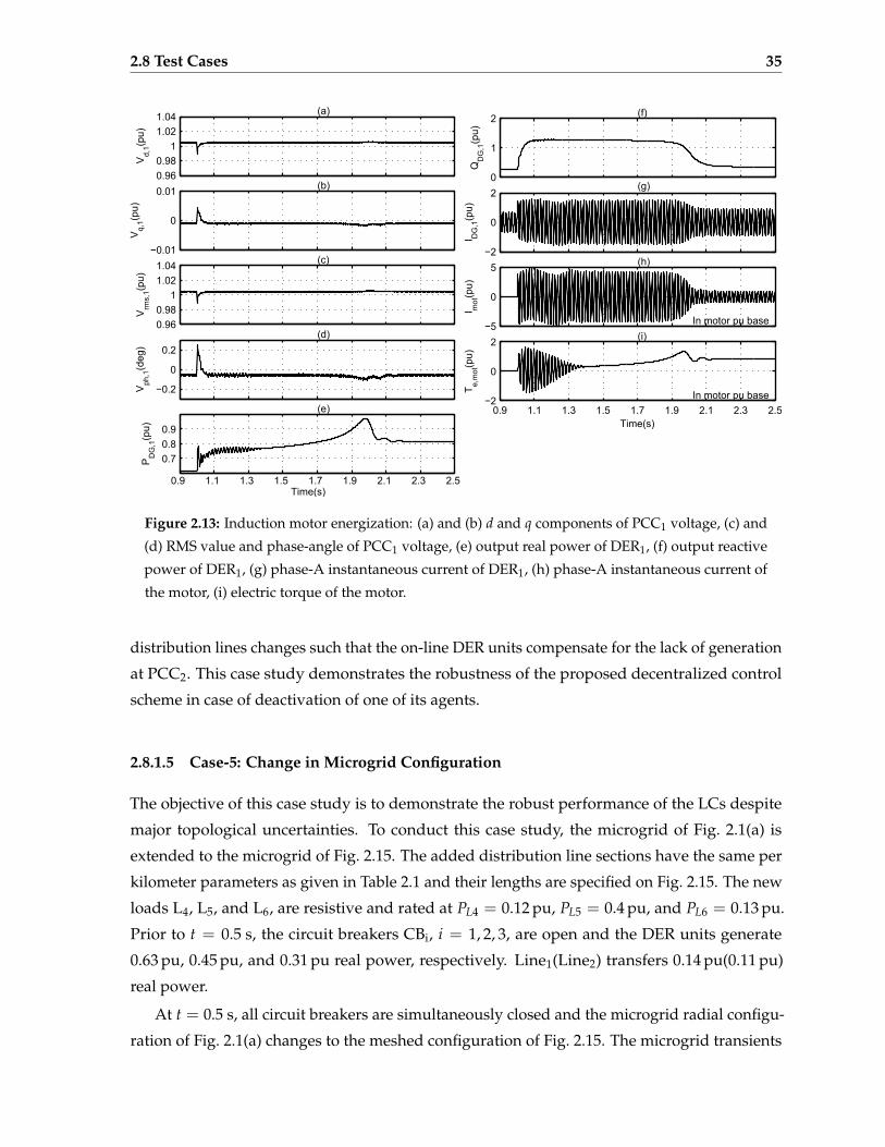
2.8 Test Cases 35
0.96
0.98
1
1.02
1.04
Vd,
1(pu)
(a)
−0.01
0
0.01
Vq,
1(pu)
(b)
0.96
0.98
1
1.02
1.04
Vrm
s,1(p
u)
(c)
−0.2
0
0.2
Vph
,1(d
eg)
(d)
0.7
0.8
0.9
PD
G,1
(pu)
(e)
0
1
2
QD
G,1
(pu)
(f)
−2
0
2
I DG
,1(p
u)
(g)
−5
0
5
I mot
(pu)
In motor pu base
(h)
0.9 1.1 1.3 1.5 1.7 1.9 2.1 2.3 2.5−2
0
2
Te,
mot
(pu)
Time(s)
(i)
In motor pu base
0.9 1.1 1.3 1.5 1.7 1.9 2.1 2.3 2.5Time(s)
Figure 2.13: Induction motor energization: (a) and (b) d and q components of PCC1 voltage, (c) and
(d) RMS value and phase-angle of PCC1 voltage, (e) output real power of DER1, (f) output reactive
power of DER1, (g) phase-A instantaneous current of DER1, (h) phase-A instantaneous current of
the motor, (i) electric torque of the motor.
distribution lines changes such that the on-line DER units compensate for the lack of generation
at PCC2. This case study demonstrates the robustness of the proposed decentralized control
scheme in case of deactivation of one of its agents.
2.8.1.5 Case-5: Change in Microgrid Configuration
The objective of this case study is to demonstrate the robust performance of the LCs despite
major topological uncertainties. To conduct this case study, the microgrid of Fig. 2.1(a) is
extended to the microgrid of Fig. 2.15. The added distribution line sections have the same per
kilometer parameters as given in Table 2.1 and their lengths are specified on Fig. 2.15. The new
loads L4, L5, and L6, are resistive and rated at PL4 = 0.12 pu, PL5 = 0.4 pu, and PL6 = 0.13 pu.
Prior to t = 0.5 s, the circuit breakers CBi, i = 1, 2, 3, are open and the DER units generate
0.63 pu, 0.45 pu, and 0.31 pu real power, respectively. Line1(Line2) transfers 0.14 pu(0.11 pu)
real power.
At t = 0.5 s, all circuit breakers are simultaneously closed and the microgrid radial configu-
ration of Fig. 2.1(a) changes to the meshed configuration of Fig. 2.15. The microgrid transients

2.8 Test Cases 36
0.95
1Vd,2(pu)
(a)
−0.02
0
0.02
Vq,2(pu)
(b)
0.96
0.98
1
Vrm
s,2(pu)
(c)
−0.2
0
0.2
Vph,2(deg)
(d)
−1
0
1
Vabc,2(pu)
(e)
0.44 0.46 0.48 0.5 0.52 0.54 0.56−0.5
0
0.5
Time(s)
PLine,i(pu)
(f)
PLine,1
PLine,2
0.44 0.46 0.48 0.5 0.52 0.54 0.56
Time(s)
Figure 2.14: DER2 accidental outage: (a) and (b) d and q components of PCC2 voltage, (c) and (d)
RMS value and phase-angle of PCC2 voltage, (e) instantaneous voltages of PCC2, (f) real power
transfer of the distribution lines.
DER1
L1DER2
L2DER3
L3L6
L5L4
CB1 CB2 CB3
2.5 km 2.5 km 5 km 5 km
15km
15km
10km
10 km
Figure 2.15: Single-line diagram of the extended microgrid to a loop configuration.
due to this switching event are illustrated in Fig. 2.16. Fig. 2.16(a)–(d) shows the d and q
components, RMS value, and phase-angle of PCC1 voltage. The specified set points for this
voltage are faithfully tracked by LC1 despite the drastic change in the configuration. Fig. 2.16(e)
and (f) shows real and reactive power generated by each DER unit. The real power transfer of
Line1 is depicted in Fig. 2.16(g) and shows an increase in the steady-state power flow of this
line due to the change in the microgrid configuration. Fig. 2.16(h) shows the real power flow
through CB1 and the corresponding line is increased to 0.21 pu.
This case study reveals the robust performance of the LCs subject to a major topological
uncertainty. Although the control scheme is designed based on the radial system of Fig. 2.1(a),
the LCs manage to maintain the stability of the microgrid after a significant configuration
change.

2.8 Test Cases 37
0.98
1
1.02
Vd,1(pu)
(a)
−0.01
0
0.01
Vq,1(pu)
(b)
1
1.005
Vrms,1(pu)
(c)
0
0.1
0.2
VPh,1(deg)
(d)
0
0.5
1
PDG,i(pu)
(e)
PDG,1
PDG,2
PDG,3
0
0.2
0.4
QDG,i(pu)
(f)
QDG,1
QDG,2
QDG,3
0
0.2
0.4
PLine,1(pu)
(g)
0.4 0.45 0.5 0.55 0.6 0.65 0.7 0.75 0.80
0.2
0.4
Time(s)
PCB1(pu)
(h)
0.4 0.45 0.5 0.55 0.6 0.65 0.7 0.75 0.8
Time(s)
Figure 2.16: Response to microgrid configuration change: (a) and (b) d and q components of PCC1
voltage, (c) and (d) RMS value and phase-angle of PCC1 voltage, (e) output real power of the three
DER units, (f) output reactive power of the three DER units, (g) real power flow on Line1, (h) real
power flow through CB1.
2.8.2 Hardware-in-the-Loop Test Cases
The test cases reported in the previous section demonstrate the feasibility of the proposed power
management scheme, the control strategy, and the open-loop frequency control for governing
dynamics of the microgrid of Fig. 2.1(a), subject to various types of uncertainties in the system.
This section presents the results of real-time simulation of the proposed control design. The
objective of this study is to verify that
• the proposed control/PMS strategy and corresponding algorithms can be digitally imple-
mented in an industrial hardware platform, and
• practical issues that do not manifest themselves in off-line simulation studies can be
readily addressed. These practical issues include noise, sampling rate of the digital
controllers, nonidealities of the SPWM signals, and nonidealities associated with A/D
and D/A conversion process.
Fig. 2.17(a) shows a schematic representation of the hardware-in-the-loop (HIL) environment
for closed-loop performance evaluation of the microgrid of Fig. 2.1(a). The system of Fig. 2.17(a)
is composed of
• an RTDS c© [73] rack that simulates the power circuitry of Fig. 2.1(a), including the interface
VSCs of the DER units, with a simulation time-step of 50 µs(3 µs) for large(small) time-step
components,

2.8 Test Cases 38
(a) (b)
A/I
D/O
FPGA
CPUD/I
NI-
cRIO
1
PWM
1
A/I
D/O
FPGA
CPUD/I
NI-
cRIO
2
PWM
2
A/I
D/O
FPGA
CPUD/I
NI-
cRIO
3
PWM
3Digital Clock for Synchronization
Analog Output Digital InputRTDS
Processing CardsV 1 V 2 V 3
Figure 2.17: Real-time simulation test bed, (a) schematic diagram, and (b) picture.
• I/O interface for signal transfer between the simulator and control platform of the DER
units,
• three NI-cRIO real-time control platforms where each NI-cRIO unit imbeds the control
algorithms of one DER unit, and
• a function generator that sends once every second a synchronization pulse to each NI-
cRIO platform to synchronize the independently generated 60 Hz phase-angle waveforms
of the DER units.
Fig. 2.17(b) shows a picture of the real-time simulation environment. Each NI-cRIO features a
real-time processor communicating with an FPGA chip via the back-plain. The FPGA chips
are used to generate the SPWM signals with the switching frequency of 6 kHz. The proposed
controller is discretized with a sampling frequency of 6 kHz and implemented in the real-
time processors using C-programming language. The 60 Hz phase-angle required for dq
transformation is generated in each NI-cRIO separately and synchronized using the external
digital signal generator that emulates a GPS. A computer emulates the PMS by performing
power flow analysis and communicating the reference set points to NI-cRIOs via Ethernet.

2.8 Test Cases 39
(a)
Vd,2
Vq,2
VABC,2
QDER,1
QDER,3
QDER,2
Switching Instant
(b)
PDER,1
PDER,3
PDER,2
IABC,2
Figure 2.18: Microgrid transients due to a load change: (a) d, q, and instantaneous components of
PCC2 voltage, and output reactive power of DER2 prior to, during, and after load change at PCC2,
(b) output real power of the three DER units and output current of DER2 in response to the load
change.
2.8.2.1 Case 6: Sudden Load Increase
In this case study, the three DER units initially deliver 0.87 pu, 0 pu, and 0.4 pu real power,
respectively. The real power flow in Line1 and Line2 is 0.1 pu. The resistive component of Load2
is suddenly increased from 0 to 0.6 pu at the time-instant denoted by “Switching Instant” in
Fig. 2.18(a). Fig. 2.18(a) illustrates the d and q components and the instantaneous voltages of

2.9 Conclusions 40
PCC2 and the output reactive power of the three DER units. It is observed that voltage signals
experience practically insignificant transients due to the effective and robust performance of
the DER controls. The output real power of the three DER units and the output current of
DER2 are depicted in Fig. 2.18(b). The output real power of DER2 increases to respond to the
increased real power demand, and those of the other DER units remain practically unchanged.
This scenario demonstrates the robustness of the proposed control scheme despite microgrid
parametric uncertainties.
2.8.2.2 Case 7: Accidental DER2 Outage
In this case study, the response of the control system to an accidental outage of DER2 is
studied. Prior to disconnection of DER2, the DER units generate 0.74 pu, 0.46 pu, and 0.15 pu
real power, respectively. The real power flow on Line1(Line2) are 0.05 pu(0.12 pu). Fig. 2.19
illustrates the transients in voltage of PCC2 and output real and reactive power of the three
DER units. Instantaneous voltages of PCC2 exhibit no significant transients since the controllers
of DER1 and DER3 rapidly increase the corresponding power generation to compensate for
the generation loss due to DER2 outage. This case study verifies the robust stability of the
decentralized control system in response to the loss of one of the decentralized control agents.
It should also be noted that during all off-line and real-time case studies, the voltage and
frequency of the system remain well within the permissible limits defined by standards and
grid codes such as IEEE 1547 [7], UL1740 [74], and the Nordic Grid Code [75].
2.9 Conclusions
This chapter presents a power management and a control strategy for an autonomous, multi-
DER microgrid. The envisioned strategy provides (i) a power management system for the
microgrid, (ii) an open-loop frequency control and synchronization, and (iii) a local, robust,
decentralized control for each DER unit. The power management system, based on the classical
power flow analysis, determines the terminal voltage set points for DER units. Frequency
of the system is controlled in an open-loop manner by utilizing an internal crystal oscillator
for each DER unit that also generates the phase-angle waveform required for dq/abc (abc/dq)
transformations. Synchronization of DER units is achieved by exploiting a GPS-based time-
reference signal. The local control of each DER unit, which is the main focus of the chapter, is
designed using a new multivariable decentralized robust control approach based on a linear
state-space model of the microgrid. Various attributes of the controller, e.g., the existence
conditions, gain-margins, robustness, and tolerance to delays are analytically discussed and the
design procedures are outlined.

2.9 Conclusions 41
(a)
VABC,2
PDER,1
PDER,2
PDER,3
QDER,1
QDER,3
QDER,2
(b)
Figure 2.19: DER2 unplanned outage: (a) instantaneous voltage of PCC2 and output real and
reactive power of the three DER units, (b) instantaneous voltage of PCC2 and its RMS value.
Analysis of microgrid dynamics highlights the robust performance of the proposed micro-
grid control scheme. Participation factors that associate closed-loop system modes and state
variables indicate that the proposed control design is a viable solution for microgrid applica-
tions. Eigenvalue sensitivity analysis results show that the the closed-loop system remains
stable for a wide range of load parametric perturbations. Robustness analysis, using the notion
of real stability radius, indicates that there is a compromise between robustness and speed of
the controllers and that the microgrid operator can tune control parameters based on microgrid
operating conditions to achieve a more robust or faster performance.

2.9 Conclusions 42
This chapter next presents the study results corresponding to the application of the proposed
power management and control system to a three-DER microgrid system. The reported results
are obtained from (i) time-domain simulation studies in the PSCAD/EMTDC platform, and
(ii) an RTDS-based hardware-in-the-loop environment. The simulation studies validate the
desired performance of the microgrid subject to load changes, voltage set point variations,
nonlinear load energization process, accidental outage of DER units, and major changes in the
microgrid topology. The test cases in the HIL environment are based on digital implementation
of the controller of each DER unit in an NI-cRIO industrial control platform and verify (i)
ease of hardware realization of the proposed power management and DER controller, and (ii)
lack of sensitivity to hardware environment issues, e.g., noise, A/D-D/A conversion process,
discretization error/delay, and PWM errors.

3 Overcurrent and
Overload Protection
3.1 Introduction
ONE OF THE microgrid control objectives, particularly in the islanded mode of operation,
is to control the PCC voltage of prespecified DER units to guarantee an overall acceptable
voltage profile. The voltage control of an electronically-coupled DER unit can be realized
either directly or through an inner current controller. The advantage of the inner current
controller [10,31,32,41,42] is that the DER unit is largely protected against fault currents since the
reference set point of the current controller restricts the phase currents within permissible values.
Thus, the DER unit can ride through faults without trip-out or damage to the unit. Likewise, the
inner current controller can limit the DER output power and prevent overloading conditions.
However, it 1) limits the speed of the overall controller and degrades its robustness due to the
need for multiple feedback loops and 2) requires both voltage and current measurements.
A direct voltage control method [15, 38, 40, 68, 69, 76–78], without the inner current control
loop, can provide a faster and a more robust performance, however, is unable to limit the
current of the voltage-controlled DER (VC-DER) unit during abnormal conditions. Thus a fault
condition can either trip out the VC-DER unit or damage its power electronic components. A
VC-DER unit is also prone to dynamic overload conditions since it inherently lacks the ability
to transiently limit the output power.
A direct voltage control method was introduced in Chapter 2. This chapter introduces two
control add-on features for this control strategy to overcome the above drawbacks of a direct
voltage control scheme:
• The first feature is an overcurrent protection scheme that operates solely based on voltage
measurements and includes 1) fault detection, 2) fault current limitation, 3) fault clearance
detection, and 4) smooth voltage control restoration mechanisms.

3.2 Voltage Control Scheme 44
Vdc
VC-DERVt
jX f
I
R f
PCC
VRemainder
of Microgrid
Microgrid
Figure 3.1: Schematic diagram of a DER unit that controls the voltage at PCC.
• The second feature is an overload protection scheme to dynamically limit the VC-DER
output power. This scheme detects overload conditions based on voltage measurements,
and limits the output power by assigning appropriate voltages to the terminals of the
interface-VSC of the DER unit.
A set of comprehensive digital time-domain simulation studies, in the PSCAD/EMTDC
platform, are performed to demonstrate performance of the proposed overcurrent and overload
protection schemes under various system transient scenarios. To verify the feasibility of the
proposed strategies, the corresponding algorithms are digitally implemented in an industrial
hardware platform, i.e., NI-cRIO controllers, and tested in the RTDS real-time simulation
environment based on the hardware-in-the-loop (HIL) approach.
3.2 Voltage Control Scheme
Fig. 3.1 illustrates a VC-DER unit, represented by a dc voltage source, a voltage-sourced
converter (VSC), and a series RL filter. The unit is interfaced to the microgrid at the point of
common connection (PCC in Fig. 3.1) through a step-up transformer. The block denoted by
“Remainder of Microgrid” in Fig. 3.1 may include current- and/or power-controlled DER units
and other components, e.g., distribution lines, loads, and capacitor banks.
A block diagram of a the direct voltage control scheme, applied to the local controller (LC)
of each VC-DER unit as described in Chapter 2, is illustrated in Fig. 3.2. The control objective is
to maintain the PCC voltage at its set point with zero steady-state error. The control function is
performed in the dq frame of reference. Three-phase instantaneous voltages of the PCC, vabc,
are measured and transformed to a dq frame of reference, Vdq, and provided to the control block.
The controller outputs, Vt,dq, are transformed to abc frame of reference taking into account the
turns ratio and phase shift of the interface transformer. Then the PWM signals are generated
based on the controller outputs, vt,abc, to synthesize the voltage at the terminal of the interface
VSC. Since the control scheme includes no inner current control loop, the VC-DER unit is subject
to overcurrent and overload during system abnormal conditions, e.g., faults.

3.3 Overcurrent Protection Scheme 45
abc/dq x = Acx + Bcu
y = Ccx + Dcu
Controller
dq/abcPWM Signal
Generator
Oscillator
vabc†
Vdq,re f
‡ ¶θ
†: Vdq
‡: Vt,dq
¶: vt,abc
Figure 3.2: Block diagram of a VC-DER voltage control scheme.
3.3 Overcurrent Protection Scheme
The objectives of the overcurrent protection scheme are to 1) limit the output current of the
VC-DER units during fault conditions by modifying voltage controller outputs and 2) restore
the controller after fault clearance. The overcurrent protection scheme is first described for
a microgrid with a single VC-DER unit and then generalized for a microgrid with multiple
VC-DER units. Both series L and LCL ac-side filter configurations are considered.
3.3.1 Microgrid with a Single VC-DER Unit
The proposed overcurrent protection scheme consists of the following.
3.3.1.1 Fault Detection
An overcurrent condition is detected based on the dynamic phasor analysis [79] by calculating
the magnitude of the VC-DER output current dynamic phasor
|I| =∣∣∣∣ Vt − VR f + jX f
∣∣∣∣ = ∣∣∣∣ ∆VR f + jX f
∣∣∣∣ , (3.1)
where1 V = Vd + jVq is the dynamic phasor of the PCC voltage and Vt = Vtd + jVtq is the
voltage controller output, Fig. 3.1.
The PCC voltage drops during a fault condition and the voltage controller, in response to
the drop, increases Vt in Fig. 3.3, which in turn increases |I|. The fault is detected when the
output current magnitude of the DER unit, calculated based on (3.1), reaches to its maximum
limit of Imax.
1Bold math symbols indicate dynamic phasors.

3.3 Overcurrent Protection Scheme 46
Re
Im
Imax =∣∣∣ ∆Vmax
R f +jX f
∣∣∣
V
V t
V t,mod
|∆V m
ax|
Figure 3.3: Dynamic phasors of a VC-DER unit, relating VSC terminal and PCC voltages.
3.3.1.2 Fault Current Limiting Scheme
To prevent an excessive output current, the outputs of the controller, Vt,dq in Fig. 3.2, are
overridden when a fault is detected and the VSC terminal voltage is set to Vt,mod, Fig. 3.3. The
circle in Fig. 3.3 encompasses all VSC terminal voltage values that result in acceptable output
current magnitudes for a given PCC voltage V . Vt,mod is calculated based on 1) the measured
PCC dynamic voltage phasor, V ; 2) the impedance between the converter terminal and the
PCC, R f + jX f ; and 3) the monitored prefault output current of the VC-DER unit, Ip f . Thus
Vt,mod = V + (R f + jX f )Ip f
ctran. (3.2)
Ip f is to keep the system operating point as close as possible to the prefault conditions and
minimize microgrid transients after the fault clearance. Constant ctran > 1 is to compensate
for the decaying dc component of the instantaneous current which is not considered by the
dynamic phasor analysis. Based on a large number of case studies, ctran = 3 is selected which
results in satisfactory performance even under worst-case scenarios.
During the time period that the overcurrent protection scheme is active, the PCC voltage
can significantly deviate from the reference set point in which case the voltage controller
accumulates error in its integrator states which is known as “integral windup” [80]. This
phenomenon can cause excessive overshoots and consequently an unacceptable transient
response after the voltage controller is restored. To avoid this situation, the integrator states of
the voltage controller are frozen when the overcurrent protection scheme is active and released
subsequent to the fault clearance.
3.3.1.3 Fault Clearance Determination and Controller Restoration
After the fault clearance, the PCC voltage increases, |I| drops below the limit Imax, and the
fault clearance is acknowledged. Then, the voltage controller is reactivated to restore voltage

3.3 Overcurrent Protection Scheme 47
tracking.
3.3.2 Microgrid with Multiple VC-DER Units
This section generalizes the proposed overcurrent protection scheme for a microgrid with
multiple VC-DER units. The fault detection and the fault current limitation schemes described
in Section 3.3.1 are equally applicable to the VC-DER units of the microgrid. However, the fault
clearance determination and controller restoration stages of each VC-DER unit require further
enhancement. The reason is that the current magnitude of the distribution line is sensitive to
the voltage difference between its two end buses, due to the distribution line small impedance.
Thus, if the controllers fail to maintain the voltage of the corresponding PCC at the set point,
the line current can exceed the DER output current limit.
In a microgrid with multiple VC-DER units, PCC voltages can significantly drift from their
set point values during a fault and thus voltage controllers need additional time to restore the
PCC voltages to the prefault values. Meantime, current magnitude can transiently exceed the
permissible value. To avoid an inadvertent fault detection as a result of current overshoots,
subsequent to a fault clearance, the voltage controllers should be smoothly restored to minimize
current transients. The following describes the fault clearance determination and smooth
controller restoration for a microgrid with multiple VC-DER units.
3.3.2.1 Fault Clearance Determination
Fault clearance instant is determined based on the PCC voltage magnitude,
Vmag =√
V2d + V2
q , (3.3)
which drops during the fault and starts increasing immediately after the fault clearance. Fault
clearance is acknowledged when Vmag has increased to a predefined level. It should be noted
that the instantaneous voltage magnitude, calculated based on (3.3), is subject to oscillatory
components during unbalanced faults. Hence, the lower envelope of Vmag is monitored and the
fault clearance is acknowledged when this envelope has increased to a predefined value.
Fig. 3.4 shows a typical PCC voltage magnitude and its lower envelope for a single-phase
to ground fault, where Vmag exhibits double-frequency oscillations. To construct Venv, the
minimum of each double frequency cycle is identified and the envelope is set to the minimum
for the next double-frequency cycle. The fault clearance is acknowledged when
Venv −Venv,min√V2
d,re f + V2q,re f
× 100 > γ, (3.4)

3.3 Overcurrent Protection Scheme 48
0.55 0.6 0.65 0.7 0.75 0.80
0.5
1
V(pu)
Time(s)
Venv
Vmag
*Venv,min
Figure 3.4: PCC voltage magnitude during a single-phase to ground fault condition and its lower
envelop.
where Venv,min is the global minimum of the envelope and γ is the percentage increase of Venv
with respect to the reference voltage set point. The reference voltage set point is selected for
calculation of γ since the actual voltage of a faulty PCC can be close to zero. Selecting higher
values for γ ensures reliable fault clearance determination; however, it reduces the restoration
speed.
3.3.2.2 Voltage Control Restoration
Restoration procedure begins after the fault clearance. This procedure is an integral part of
the overcurrent protection scheme for a microgrid with multiple VC-DER units to ensure the
controllers are smoothly restored and current transients are limited within the permissible
range. The procedure depends on the relative difference between the prefault and postfault
operating points of the VC-DER unit and two conditions can occur:
A1) The postfault operating point can be approximately the same as the prefault point. This is
the case when the fault 1) is temporary and clears itself without any line or generation
outage, i.e., 80–90% of the faults in distribution systems [81], 2) is permanent but its
clearance does not significantly change the VC-DER unit output power.
A2) The postfault operating point can significantly deviate from the prefault operating point.
This is the case when the fault is permanent and its clearance entails a significant change
in the VC-DER unit output power.
To determine which one of the above has occurred, the output current of the VC-DER unit,
which was limited to Ip f /ctran during fault based on (3.2), is gradually increased until the
magnitude of the corresponding PCC voltage is almost the same as the prefault value. The
corresponding VC-DER unit output current is Irs, and the relative difference between Irs and
Ip f is
∆I =
√(Re(Irs)−Re(Ip f ))2 + (Im(Irs)− Im(Ip f ))2
|Irs|. (3.5)
3.3 Overcurrent Protection Scheme 49
∆I is compared with a tolerance level, ∆Itol , to determine which one of the above conditions
holds. ∆Itol depends on the system and the controllers parameters. Based on extensive case
studies, ∆Itol = 0.1 is selected for the reported studies.
To accommodate reclosure operations, the overcurrent protection scheme waits in restora-
tion state until the microgrid protection scheme acknowledges the reclosure operation has been
completed. Depending on which one of A1 or A2 conditions holds, the overcurrent protection
scheme proceeds to restore the normal voltage control as follows.
A1 holds) In this case, Vt has been already modified such that output current of the VC-
DER unit is Ip f and the system should be given enough time to reach its steady state. Since
the postfault operating point is almost identical to the prefault operating point and the state
variables of the controllers were frozen during the fault and the restoration stages, the controller
is smoothly restored.
A2 holds) In this case the controller restoration may result in excessive overshoot of the VC-
DER output current which, in turn, can be mistakenly interpreted as a fault condition. To avoid
this scenario and achieve a controller smooth restoration with minimum current transients, the
VC-DER whose operating point has significantly changed is temporarily disconnected and then
the following two steps are taken:
1. The voltage reference for the controller is set at the current PCC voltage.
2. The state variables of the controller are initialized such that the the outputs of the controller
before and after its restoration are equal. This is achieved by a state observer which is
designed based on the state-space parameters of the voltage controller Ac, Bc, Cc, and Dc
in Fig. 3.2. The observer inputs are (i) Vtd and Vtq at the end of restoration stage, (ii) the
measured PCC voltage, and (iii) the reference set points. The output of the observer is the
state vector x that determines the initial conditions for the state variables of the voltage
controller. Details of designing such an observer are described in Chapter 5.
The voltage controller then receives updated set points from the power management system
and provides tracking. The VC-DER unit can be subsequently reconnected to the microgrid
based on a command from the power management system. Fig. 3.5 illustrates a flowchart of
the voltage control scheme, including the overcurrent protection mechanism.
3.3.3 VC-DER Units with LCL Filters
The interface VSC filter is either a series RL filter, Fig. 3.1, or a T-shape LCL filter, Fig. 3.6. The
proposed overcurrent protection scheme of Section 3.3.1 can be readily applied to a DER unit

3.3 Overcurrent Protection Scheme 50
|I| < Imax? Normal Control Action
Limit Fault CurrentRestore PCC Voltage
Magnitude Based on (2)
Fault Cleared? Reclosing?
∆I > ∆Itol?
Reconnect VC-DER Disconnect VC-DER
Track Updated Set PointsRestore Normal Voltage
Control
YesNo
NoYes
Yes No
YesNo
Figure 3.5: Flowchart of the voltage control scheme including the overcurrent protection.
Vdc
VC-DERVt
jX f ,L1
I
jX f ,L2
jX f ,C PCC
VRemainder
of Microgrid
Microgrid
Figure 3.6: Schematic single-line diagram of a DER unit equipped with an LCL filter.
with a T-shape LCL filter by replacing (3.1) and (3.2) with
|Ilin| =
∣∣∣∣∣∣Vt
(1 + X f ,L2
X f ,C
)− V
X f ,L1 + X f ,L2 +X f ,L1X f ,L2
X f ,C
∣∣∣∣∣∣ , (3.6)
and
Vt,mod =
Ip fctran
(X f ,L1 + X f ,L2 +
X f ,L1X f ,L2X f ,C
)+ V
1 + X f ,L2X f ,C
, (3.7)
respectively, where (3.6) and (3.7) are derived based on dynamic phasor analysis of the circuit of
Fig. 3.6. Since the series impedances are highly inductive, the resistive components are ignored
in the analysis.

3.4 Overload Protection 51
3.4 Overload Protection
The objective of the overload protection scheme is to limit the output power of a VC-DER unit
whose controller does not include an inner current control loop. The instantaneous three-phase
apparent output power of the DER unit of Fig. 3.1, based on dynamic phasors, is expressed as
S = 3V I∗ = 3V∣∣∣∣ Vt − VR f + jX f
∣∣∣∣∗ = 3V∣∣∣∣ ∆VR f + jX f
∣∣∣∣∗ . (3.8)
Based on the maximum generation capacity of the unit, Smax, the impedance R f + jX f , and the
PCC voltage V , the maximum magnitude of the voltage difference, ∆Vmax, that corresponds to
the maximum output power is
∆Vmax =Smax|R f + jX f |
3|V | . (3.9)
Thus the VC-DER unit is overloaded if |∆V | > ∆Vmax and leads to the following overload
protection strategy. The magnitude
|∆V | =√(Vtd −Vd)2 + (Vtq −Vq)2, (3.10)
is compared with ∆Vmax. If |∆V | > ∆Vmax, the output of the voltage controller is ignored and
the terminal voltage, in the dq reference frame, is assigned based on (3.9) and the measured PCC
voltage Vdq. The area within the circle of Fig. 3.3 identifies all |∆V | that result in an acceptable
amount of output power. To maximize the output power of the unit, ∆V with the magnitude
of ∆Vmax is selected. To operate as close as possible to the operating point that the voltage
controller has specified, the angle of ∆V is selected such that the distance between Vt,mod and
Vt, Fig. 3.3, is minimized, i.e.,
Vtd,mod = Vd + ∆Vmax cos(
tan−1 Vtq −Vq
Vtd −Vd
),
Vtq,mod = Vq + ∆Vmax sin(
tan−1 Vtq −Vq
Vtd −Vd
).
(3.11)
This will limit the output power of the DER unit to Smax. When the output power is limited, the
integrator states of the voltage controller are kept unchanged to avoid integral windup. The
microgrid power management system resolves the overloading condition of the DER unit as
fast as possible, e.g., by either load shedding or power flow alteration. The voltage controller
can then be restored and since the integral windup has been avoided, the system continues
operating with minimum transients. This scheme is an integral part of the voltage controllers
of all VC-DER units of the microgrid.

3.5 Performance Evaluation 52
0.55 0.6 0.65 0.7 0.75 0.8−20
−10
0
10
20
I 1,ab
c(pu)
Time(s)
Figure 3.7: Three-phase output currents of DER1 during a fault while the overcurrent protection
scheme is disabled.
3.5 Performance Evaluation
This section presents the results of offline time-domain and real-time HIL simulation case
studies to demonstrate performance and feasibility of the proposed overcurrent and overload
protection algorithms.
3.5.1 Offline Time-domain Simulation Studies
A set of test cases, based on digital time-domain simulation studies in the PSCAD/EMTDC
environment, were carried out to evaluate performance of the proposed overcurrent/overload
protection strategies. The component models and parameter values are the same as those of
Chapter 2. The overcurrent/overload protection feature for each LC is coded in FORTRAN and
imbedded in the FORTRAN-code implementation of the corresponding controller.
3.5.1.1 Case 1: Overcurrent Protection – Temporary Fault
This case study demonstrates 1) performance of the overcurrent protection scheme in limiting
the VC-DER output current when the microgrid is subject to a three-phase temporary fault
and 2) restoration of the normal control action subsequent to the fault clearance. Before fault
inception, the three DER units deliver 1 pu, 0.75 pu, and 0.35 pu apparent power at a 0.94, 0.96,
and 0.92 lagging power factor, respectively. The real power transfers of Line1 and Line2 are
0.1 pu and 0.15 pu, respectively. At t = 0.6 s, a bolted temporary three-phase to ground fault
at PCC1 occurs and lasts for 5 cycles. The fault at PCC1 results in the most severe overcurrent
with respect to DER1. Fig. 3.7 shows the output current of DER1 prior to, during, and after the
fault while the overcurrent protection scheme is disabled. Provided DER1 could withstand the
overcurrent, the peak current reaches 18 pu. In practice, this output current magnitude either
damages the power electronic switches or trips out the DER unit.
Fig. 3.8 illustrates the microgrid transients prior to, during and subsequent to the same
fault while the overcurrent protection scheme is in service. Fig. 3.8(a) and (b) shows that PCC1

3.5 Performance Evaluation 53
−1
0
1
V1,
abc(p
u)
(a)
−1
0
1
V2,
abc(p
u)
(b)
−1
0
1
I 1,ab
c(pu)
(c)
0.6 0.65 0.7 0.75 0.8
−1
0
1
I 2,ab
c(pu)
(d)
Time(s)
Figure 3.8: Performance of the overcurrent protection scheme for an L-L-L-G fault at PCC1: (a) and
(b) three-phase voltages of PCC1 and PCC2, (c) and (d) three-phase output currents of DER1 and
DER2.
and PCC2 voltages significantly decrease during the fault and are smoothly restored to their
prefault reference set points subsequent to the fault clearance. Fig. 3.8(c) and (d) shows that the
instantaneous three-phase output currents of DER1 and DER2 are effectively limited during the
fault (compare with Fig. 3.7) and increase to their prefault steady-state values after the fault
clearance. The maximum permissible current magnitude for each DER unit is assumed to be
2 pu, based on the unit ratings.
Similar test cases were carried out when the DER units were equipped with LCL filters, and
the modified overcurrent protection scheme of Section 3.3.3 was in service and results similar
to Fig. 3.8 were obtained. Extensive case studies for different fault types and locations were
conducted which demonstrated the ability of the overcurrent protection method in 1) detecting
a fault condition, 2) limiting the output current magnitudes of DER units, and 3) restoring the
microgrid to its prefault operating conditions.

3.5 Performance Evaluation 54
3.5.1.2 Case 2: Overcurrent Protection – Successful Reclosure
The objective of this case study is to demonstrate performance of the overcurrent protection for
a temporary fault and its subsequent successful reclosure event. Prior to the fault, the three
DER units deliver 0.71 pu, 0.43 pu, and 0.54 pu apparent power at 0.93, 1.00, and 0.92 lagging
power factor, respectively, and 0.25 pu (0.1 pu) real power is transferred by Line1 (Line2). At
t = 0.6 s, a single-phase to ground temporary fault occurs at the middle of Line1. The breakers
at both ends of Line1 are opened after 5 cycles at t = 0.68 s and remain open for 15 cycles. The
temporary fault is self-cleared prior to the reclosing attempt at t = 0.93 s. Since the reclosure is
successful, the microgrid continues its operation at an operating point identical to its prefault
conditions.
Fig. 3.9 illustrates instantaneous three-phase PCC voltages and output currents correspond-
ing to the three DER units, prior to, during and subsequent to the fault and its subsequent
switching events. Fig. 3.9 shows that the fault is detected within about 500 µs, the output
currents of the DER units are effectively limited during the fault to less than 1.2 pu, the original
controllers are restored at about t = 1 s, and the PCC voltages are maintained at the prefault
values.
3.5.1.3 Case 3: Overcurrent Protection – Unsuccessful Reclosure
The prefault system operating condition and the fault scenario are the same as those of previous
case study. However, the fault is permanent and the reclosure at t = 0.93 s is unsuccessful.
Thus, the breakers are reopened after 5 cycles at t = 1.01 s and are locked out subsequently.
The microgrid operation continues subsequent to fault clearance while Line1 is open, and the
three DER units generate 0.48 pu, 0.62 pu, and 0.46 pu apparent power at a 0.83, 1.00, and 0.94
lagging power factor, respectively. Since the power transfer on Line1 is interrupted due to line
outage, the operating point of DER2 is significantly changed, and based on the discussion of
Section 3.3.2.2, DER2 is disconnected by opening Line2. After the restoration of LC2, Line2 can
be closed to connect the unit to the system.
Fig. 3.10 illustrates the microgrid transients, i.e., instantaneous three-phase PCC voltages,
output currents of the three DER units, and power transfer on Line1 in response to the fault
and its subsequent switching events. Fig. 3.10 shows that the overcurrent protection scheme
effectively limits DER output currents both at the inception of fault and at the unsuccessful
reclosure instant. Fig. 3.10 indicates 1) the current transients are restricted within the permissible
limits, 2) the restoration procedure successfully restores the controllers to track the voltage set
points after the fault clearance, and 3) the current transients are within the acceptable range
during the restoration process.

3.5 Performance Evaluation 55
−1
0
1
V1,
abc(p
u)
(a)
−1
0
1
I 1,ab
c(pu)
(b)
−1
0
1
V2,
abc(p
u)
(c)
−1
0
1
I 2,ab
c(pu)
(d)
−1
0
1
V3,
abc(p
u)
(e)
0.55 0.65 0.75 0.85 0.95 1.05−1
0
1
I 3,ab
c(pu)
(f)
Time(s)
Figure 3.9: Performance of the overcurrent protection scheme for a temporary L-G fault at the
middle of Line1 and its subsequent single-pole successful reclosure: (a) – (f) three-phase PCC
voltages and output currents of the three DER units.
3.5.1.4 Case 4: Overload Protection
This case study demonstrates the effectiveness of the proposed overload protection scheme,
Section 3.4. Initially, the DER units supply the microgrid net load proportional to their maximum
generation capacities. At t = 0.5 s, real component of Load1 increases to 0.9 pu, which is beyond
the generation capacity of DER1. Fig. 3.11 shows that output power of DER1 is limited to its
maximum generation capacity by the overload protection method and the other DER units
automatically increase their output power to meet the demand. At t = 1 s, the PMS updates
the voltage reference set points to alter the power flow within the microgrid such that the
output power of DER1 does not exceed its permissible limit. Fig. 3.12 shows the instantaneous
three-phase voltages of PCC1 and PCC2 for the same period of time and indicates acceptable
voltage waveforms for the entire period.
To illustrate the effect of integral windup, the same test case is carried out while the
integrator states of the LC are not frozen when the overload protection scheme is active. Fig.
3.13 shows excessive overshoots at t = 1 s when the LCs are restored. A comparison between

3.5 Performance Evaluation 56
−1
0
1
V1,abc(pu)
(a)
−101
I 1,abc(pu)
(b)
−1
0
1
V2,abc(pu)
(c)
−101
I 2,abc(pu)
(d)
−1
0
1
V3,abc(pu)
(e)
−101
I 3,abc(pu)
(f)
0.5 0.6 0.7 0.8 0.9 1 1.1 1.2 1.3−0.200.20.4
P,Q Line1(pu)
(g)
Time(s)
PQ
Figure 3.10: Performance of the overcurrent protection scheme for a permanent L-G fault at the
middle of Line1: (a) – (f) three-phase PCC voltages and output currents of the DER units, and (g)
real and reactive power transfer of Line1.
the corresponding transients of Figs. 3.11 and 3.13 reveals the necessity of the anti-windup
scheme for a smooth restoration process.
3.5.2 Hardware-in-the-loop Simulation Test Case
The objective of this study is to verify that the proposed overcurrent/overload protection
schemes can be digitally implemented in an industrial hardware platform despite hardware
implementation issues, e.g., noise, sampling rate of the digital controllers, sample and hold of
SPWM signals, delay and nonzero bias of analog inputs and outputs, and discretization errors
that do not manifest themselves in off-line simulation studies. HIL environment, component
models, and parameter values are the same as those of Chapter 2, as described in Section 2.8.2.
Overcurrent/overload protection scheme of each VC-DER unit is imbedded in the C-code
implementation of the corresponding voltage controller.

3.5 Performance Evaluation 57
0.4 0.6 0.8 1 1.20
0.5
1
1.5
S DE
R,i(p
u)
Time(s)
SDER,1
SDER,2
SDER,3
Figure 3.11: Apparent output power of the three DER units when Load1 increases beyond the
maximum generation capacity of DER1.
−1
0
1
V1,
abc(p
u)
(a)
0.5 0.6 0.7 0.8 0.9 1−1
0
1
V2,
abc(p
u)
(b)
Time(s)
Figure 3.12: Three-phase voltages of PCC1 and PCC2 while overload protection scheme in service.
3.5.2.1 Case 5: Overcurrent Protection – Temporary Fault
Fig. 3.14 shows the system response, i.e., DER1 instantaneous voltages and currents, to a
three-phase temporary fault at PCC1. Prior to the fault inception, the microgrid supplies the
loads and LCs maintain voltages of PCC at the prespecified set points. Fig. 3.14 shows that
voltage drops to zero due to the fault and the overcurrent protection scheme effectively limits
the output current magnitude. After the fault clearance, the voltages are restored to prefault
steady-state value.
Fig. 3.15 illustrates the fault inception and fault detection instants. Fig. 3.15 indicates
0.4 0.6 0.8 1 1.2
0
1
2
3
S DE
R,i(p
u)
Time(s)
SDER,1
SDER,3
SDER,2
Figure 3.13: Power transients subsequent to restoration of LC1 while the anti-windup scheme is
disabled.

3.6 Conclusions 58
Vabc
Iabc
Figure 3.14: Transients of PCC1 voltages and DER1 output currents due to a L-L-L-G fault at PCC1.
Fault inception instant
Fault detection instant
Figure 3.15: Fault detection speed of the proposed overcurrent protection scheme.
that the fault detection scheme, based on instantaneous voltage measurements, can detect the
three-phase to ground fault in less than 200 µs. This is significantly faster than a conventional
overcurrent relay whose response time is in the range of 15 ms to 50 ms. Due to its speed, the
proposed fault detection scheme can be implemented for applications that require fast fault
detection.
3.6 Conclusions
This chapter presents two new concepts for overcurrent and overload protection to enable direct
voltage control of electronically-coupled DER units in an islanded microgrid. The overcurrent
protection scheme detects the fault, limits the DER unit output current magnitude within its
permissible range, e.g., 1.2 pu, and restores the microgrid to its normal operating condition
subsequent to the fault clearance. The fault detection scheme can detect a fault in 200 µs; thus

3.6 Conclusions 59
it can be implemented in protective relays where speed is a concern. The overload protection
scheme limits the output power of the DER unit to its rated MVA when excessive power
demand is imposed on the DER unit. An extensive set of time-domain simulation studies in
the PSCAD/EMTDC platform and an RTDS-based hardware-in-the-loop environment were
performed to evaluate and verify the feasibility of the proposed schemes.
The study results demonstrate the desired performance of the add-on features when the
microgrid is subject to various types of faults and the subsequent fault overcurrent/overload
conditions. The real-time case study demonstrates 1) ease of hardware realization of the pro-
posed methods, and 2) lack of sensitivity to noise, A/D-D/A conversion process, discretization
error/delay, and PWM errors. In the reported studies, the proposed schemes are used to limit
the 1) overcurrent to 1.2 pu and 2) overload to the DER unit maximum generation capacity, in a
microgrid with three DER units.
4 Generalized
Microgrid Control
4.1 Introduction
AMICROGRID control strategy is proposed in Chapter 2 and applied to a three-DER mi-
crogrid where each DER unit controls the voltage of its point of common coupling (PCC).
This chapter generalizes the approach of Chapter 2, based on the same robust decentralized
control scheme, such that 1) each DER unit can now be designated as a voltage-controlled
(VC-DER) or a power-controlled (PC-DER) unit depending on microgrid configuration, DER
unit location, load information, and other possible considerations; 2) more than one DER unit
can contribute to voltage regulation if the distribution feeder is long and/or heavily loaded;
and 3) none of the DER units is assumed to be dominant.
The strategy proposes that (i) a PMS should specify voltage and power set points for the
corresponding DER units, (ii) local controllers (LCs) should provide tracking of the set points,
and (iii) an open-loop frequency control and synchronization scheme should maintain the sys-
tem frequency. This method provides prescribed load sharing among DER units, precise power
flow regulation, robust tracking of set points, operation with no need for high-bandwidth com-
munication, and a fixed microgrid frequency. The proposed approach requires low-bandwidth
communication for both synchronization and PMS data transmission. However, temporary fail-
ure of communication does not lead to system collapse, provided it recovers prior to significant
changes in the microgrid operating point.
A set of eigenvalue and robustness studies are performed to signify the properties of the
proposed controllers. A set of comprehensive digital time-domain simulation studies, in the
PSCAD/EMTDC platform, are performed to demonstrate performance of the proposed scheme.
To verify performance of the hardware-implemented strategy, its algorithms are digitally
implemented in an industrial platform and tested in a real-time simulation environment based
on the hardware-in-the-loop (HIL) approach.

4.2 Study System 61
(a)
L2 L4
L5 L1
L1
2 km 2 km
2 km 7 km
2 km
CB1
L2
3 km
2 km
L3
L3L3
L1
L2
Bm
2 km
2 km
4 km 3 km
4 km
DER1 DER2
DER3
220 kV/13.8 kV
CBg
Grid
(b)
Vdc
DERiVt
jX
I
R
PCC
V
Figure 4.1: (a) A schematic diagram of the studied microgrid system, (b) configuration of each DER
unit.
4.2 Study System
A schematic diagram of a distribution system that is adopted as the study microgrid system
is illustrated in Fig. 4.1(a). The distribution system of Fig. 4.1(a) is selected since it includes a
relatively large number of buses, feeder branches, and electric loads and it provides a more
realistic environment to evaluate performance of the controllers. The microgrid includes three
0.6 kV dispatchable electronically-interfaced DER units and eleven loads which are connected
to a 13.8 kV distribution system. Each DER unit is represented by a 1.5 kV DC voltage source,
a two-level voltage-sourced converter (VSC), and a series RL filter, and is interfaced to the
distribution feeder by a 0.6 kV /13.8 kV step-up transformer at its PCC, Fig. 4.1(b). The system
data are given in Table 4.1. The microgrid is operated in islanded mode by opening the circuit
breaker CBg.

4.3 Power Management and Control Strategy 62
Table 4.1
MICROGRID DATA, Sbase = 1.6 MVA, Vbase = 13.8 kV
Size of DER Units
DER1: 1.6 MVA DER2: 1.2 MVA DER3: 0.8 MVA
Load Data: Li(MVA-power factor)
L1(0.08-0.94) L2(0.16-0.98) L3(0.16-0.90) L4(0.17-0.94) L5(0.25-0.96)
Line Impedance: (0.35 + j0.31)Ω km−1
Transformer Reactance: 8 %
RL filter: Z =15 %, Quality factor= 50
4.3 Power Management and Control Strategy
The proposed strategy is composed of (i) a power management system (PMS), (ii) a microgrid
frequency control and the associated synchronization scheme, and (iii) local controllers (LCs) of
DER units.
4.3.1 Power Management System
DER1 and DER3 are designated as power-controlled DER (PC-DER) units, i.e., their real/reactive
output power components are controlled, and DER2 is a voltage-controlled DER (VC-DER) unit,
i.e., it regulates the voltage of its PCC, and as a result, the voltage profile of the entire microgrid.
DER2 is designated as a VC-DER unit due to its location in the studied microgrid system,
Fig. 4.1(a). In general, to improve the overall voltage profile of the microgrid, depending
on the distribution feeder length, configuration, and load information, multiple DER units
can be assigned as VC-DER units and others can operate as PC-DER units. To determine
appropriate real/reactive power set points for PC-DER units, the microgrid is continuously
monitored, its net load is measured, and the collected data is communicated to the central
PMS through a low-bandwidth communication link. Based on the measured total real/reactive
power components of the microgrid load and a prescribed load sharing scheme, the PMS
determines the real/reactive power set points for PC-DER units, Pref,i and Qref,i, i = 1, 3. The
PMS also specifies an appropriate voltage set point, e.g., 1∠0, for the VC-DER unit (DER2). By
maintaining the voltage of its PCC, DER2 delivers
PDER,2 = PLoad + PLoss − PDER,1 − PDER,2,
QDER,2 = QLoad + QLoss −QDER,1 −QDER,2,(4.1)

4.3 Power Management and Control Strategy 63
where PLoad/QLoad are the total real/reactive power demand of microgrid net load and PLoss/
QLoss are the total real/reactive power loss of the distribution feeder. Thus, the PMS regulates
the power flow of the microgrid. The power management process should be performed
frequently to maintain the prespecified load sharing scheme among the DER units as the
microgrid operating point changes, e.g., due to load and generation changes.
4.3.2 Frequency Control and Synchronization
The frequency control and synchronization scheme of Section 2.3.2 is equally applicable for this
control strategy and adopted for the reported studies of this chapter.
4.3.3 Local Controllers
The power and voltage set points are transmitted from the PMS to each DER LC. Since LCs
perform the control in a dq frame of reference, the set points should be first transformed to the
dq frame based on the globally synchronized phase-angle waveform θ(t). For the VC-DER unit,
the set point V∠δ is expressed as Vd,re f = V cos δ and Vq,re f = V sin δ in the dq frame. For the
PC-DER units, since the LCs provide tracking of their output current components Id and Iq, the
real/reactive power set points should be first expressed in terms of current set points Id,re f and
Iq,re f using
Idi,re f =23
(VdiPre f ,i + VqiQre f ,i
V2di + V2
qi
),
Iqi,re f =23
(VqiPre f ,i −VdiQre f ,i
V2di + V2
qi
),
(4.2)
where Vdi and Vqi are the dynamic d and q voltage components of PCCi. The measured
and reference signals are then provided to LCi, whose outputs Vtd,i and Vtq,i are the d and q
voltage components of DERi VSC interface-terminal with respect to the high-voltage side of the
transformer. Vtd,i and Vtq,i are then transformed to abc frame, divided by the turn ratio of the
transformer and shifted, if necessary, to obtain vt,abc,i,LV corresponding to the low-voltage side
of the transformer. vt,abc,i,LV is then fed to the PWM signal generator of the interface VSC. Fig.
4.2 illustrates a block diagram of LCi which applies for both voltage and current control loops.
To design parameters of the three LCs, a mathematical model of the open-loop microgrid is
required. A microgrid generally includes a large number of loads, distribution line segments,
and DER units which drastically increase the order of its mathematical model. Hence, it is
desirable to develop a low order model of the system for control design. Due to the robustness
of the proposed control scheme, potential discrepancies between the low order model and the
detailed higher-order model cannot significantly impact on controller performance or cause

4.3 Power Management and Control Strategy 64
B∫
K3
A
∫K2
K1
abc/dq
abc/dqTransformer Turn
Ratio and Phase Shift
Compensation
dq/abc
PWM Signal
Generator
VSC of DERi
β
+ +
+
+ +
Vtdq,i
η
+
vtabc,i,HV
vtabc,i,LV
+
Xdq,re f ,i−
xabc,i
|Xdq,re f ,i|∠δi
Figure 4.2: Block diagram of LCi where x and X can represent either voltage or current in abc and
dq frames of reference, respectively.
instability. To develop a low order equivalent linear model, the microgrid of Fig. 4.1(a) is
approximated by a radial distribution feeder with the three DER units interconnected through
two distribution line segments while their electrical distance is preserved. Loads electrically
close to each unit are combined and connected to the corresponding PCC. A single-line diagram
of the simplified microgrid is shown in Fig. 2.4. Each DER unit is represented by a three-phase
controlled voltage source and a series RL branch. Each load is modeled by an equivalent parallel
three-phase RLC network. Each distribution line is represented by lumped series three-phase
RL elements. Parameters of the model are given in Table 2.1. The controllers are designed
based on the fundamental frequency component of the microgrid model, Fig. 2.4. Thus, the
mathematical model of Section 2.4 is equally applicable in this case as well, except for the
following: 1) yT in (2.6) is modified to yT =(
I1,d, I1,q, V2,d, V2,q, I3,d, I3,q); 2) yi in (2.7) is modified
to yi = (Ii,d, Ii,q), i = 1, 3; and 3) the output matrix C′ in Appendix A, instead of C, is used.
Carrying out the optimization of the controller (2.15), as measured by the performance
index (2.17), yields the following decentralized controller for the microgrid of Fig. 4.1(a):
η = y− yre f ,
β = Aβ +By,
u = K1y +K2η +K3β,
(4.3)
where
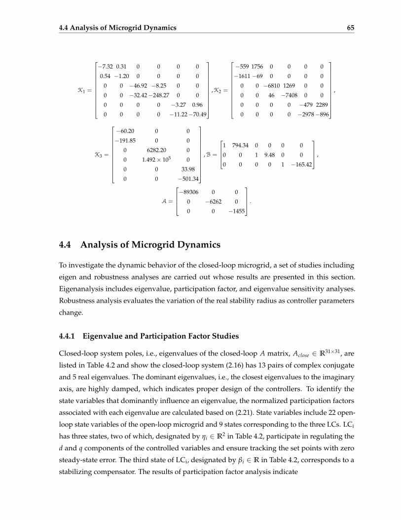
4.4 Analysis of Microgrid Dynamics 65
K1 =
−7.32 0.31 0 0 0 0
0.54 −1.20 0 0 0 0
0 0 −46.92 −8.25 0 0
0 0 −32.42−248.27 0 0
0 0 0 0 −3.27 0.96
0 0 0 0 −11.22−70.49
,K2 =
−559 1756 0 0 0 0
−1611 −69 0 0 0 0
0 0 −6810 1269 0 0
0 0 46 −7408 0 0
0 0 0 0 −479 2289
0 0 0 0 −2978−896
,
K3 =
−60.20 0 0
−191.85 0 0
0 6282.20 0
0 1.492× 10⁵ 0
0 0 33.98
0 0 −501.34
,B =
1 794.34 0 0 0 0
0 0 1 9.48 0 0
0 0 0 0 1 −165.42
,
A =
−89306 0 0
0 −6262 0
0 0 −1455
.
4.4 Analysis of Microgrid Dynamics
To investigate the dynamic behavior of the closed-loop microgrid, a set of studies including
eigen and robustness analyses are carried out whose results are presented in this section.
Eigenanalysis includes eigenvalue, participation factor, and eigenvalue sensitivity analyses.
Robustness analysis evaluates the variation of the real stability radius as controller parameters
change.
4.4.1 Eigenvalue and Participation Factor Studies
Closed-loop system poles, i.e., eigenvalues of the closed-loop A matrix, Aclose ∈ R31×31, are
listed in Table 4.2 and show the closed-loop system (2.16) has 13 pairs of complex conjugate
and 5 real eigenvalues. The dominant eigenvalues, i.e., the closest eigenvalues to the imaginary
axis, are highly damped, which indicates proper design of the controllers. To identify the
state variables that dominantly influence an eigenvalue, the normalized participation factors
associated with each eigenvalue are calculated based on (2.21). State variables include 22 open-
loop state variables of the open-loop microgrid and 9 states corresponding to the three LCs. LCi
has three states, two of which, designated by ηi ∈ R2 in Table 4.2, participate in regulating the
d and q components of the controlled variables and ensure tracking the set points with zero
steady-state error. The third state of LCi, designated by βi ∈ R in Table 4.2, corresponds to a
stabilizing compensator. The results of participation factor analysis indicate

4.4 Analysis of Microgrid Dynamics 66
• all closed-loop eigenvalues are contained in the open left-half complex plain and are far
from the imaginary axis, thus the closed-loop system is stable and well-damped,
• dominant eigenvalues of the closed-loop system, i.e., eigenvalues 1–8, are predominantly
affected by the controller regulating states,
• state variables corresponding to Vdq2 are associated with the eigenvalues which are far
from the imaginary axis and have fast dynamics,
• stabilizing compensator states have very fast dynamics which is desirable,
• state variables corresponding to DER output and load currents are associated with rela-
tively slow modes which is expectable due to the large time-constant of the corresponding
inductors, and
• state variables corresponding to distribution line currents are associated with faster modes
due to the low X/R ratio of the distribution line.
These observations suggest that the optimal control design procedure meets requirements for a
generalized islanded microgrid control problem.
In another study, the controller parameters Ki are scaled by parameter αi and corresponding
eigenvalue trajectories are illustrated in Fig. 4.3. Fig. 4.3(a) shows that eigenpairs (5,6) and
(18,19) depart to the right-hand-side as α1 is decreased from 1 to 0.8 and the departure to the
right-half complex plane occurs at α1 = 0.92. It is also observed the closed-loop system becomes
unstable for α1 > 144. Fig. 4.3(b) shows that eigenpairs (1,2) and (5,6) move towards the
imaginary axis as α2 is increased in the range 0.1 < α2 < 2 and depart to the right-hand-side
when α2 = 1.61. Fig. 4.3(c) shows that the eigenpair (11,12) exhibits higher damping as α3
is increased in the range 0.8 < α3 < 1.2 and departs to the right-hand-side at α3 = 1.09.
Similar results are obtained for K4. Fig. 4.3(d) shows that eigenpairs (11,12) and (5,6) move
further away from the imaginary axis and become more damped as α5 is increased in the
range 0.8 < α5 < 1.2 and the closed-loop system is unstable for α5 < 0.91. This study shows
the range of variations of controller parameters which results in a stable closed-loop system.
Similar eigenvalue sensitivity analysis was carried out for load parameter perturbations. It was
observed that for a wide range of load parameter perturbations, the closed-loop eigenvalues
remain in open left-half complex plane which highlights robust performance of the controllers.
Next section presents robustness analysis studies of the closed-loop system.

4.4 Analysis of Microgrid Dynamics 67
Table 4.2
EIGENVALUES OF THE CLOSED-LOOP SYSTEM AND THE ASSOCIATED PARTICIPATING STATES
Number Eigenvalue Participating States
1,2 -18.01 ± 377.75i Idq1, η1
3,4 -18.54 ± 377.13i η2, η3
5,6 -22.22 ± 371.74i η3, ILq3
7,8 -43.45 ± 6.22 i η1
9 -55.87 Iq2, ILq2
10 -65.45 Id3, η3
11,12 -81.19 ± 375.4i Id1, ILd3
13,14 -87.54 ± 369.34i Idq1
15 -128.09 ILd3, Id3
16,17 -346.34 ± 1755i Iq3, β3
18,19 -445.41 ± 344.4i η2, β2
20,21 -488.95 ± 4317i Vd2, Itd1
22,23 -547.8 ± 2560i Vq1, Itq1
24,25 -610.97± 1792.6i Vd3
26,27 -806.45 ± 1048.7i Iq2, β2
28 -1846.4 Iq2, β2
29,30 -20763. ± 6130i Vq2, Iq2
31 -89282 β1
4.4.2 Robustness Analysis
Subsequent to a control design, it is required the closed-loop system should be robust, i.e., the
state matrix of the closed-loop system should preserve its stability property when its elements
are perturbed. The notion of real stability radius, defined in Section 2.5.3, is used to evaluate
the robustness of the closed-loop system as control parameters are perturbed.
In this part, the effect of controller parameter variations on the real stability radius, rR, of the
closed-loop system state matrix, Aclose, is studied. The matrix triple Aclose, [A, A, 0]T, [I, 0, 0]is considered as the argument of function rR(.) in (2.12) to reflect microgrid load uncertainties.
Fig. 4.4 illustrates the variations of rR and closed-loop system maximum settling time as the
controller parameter K2 changes to αK2 for 0.1 < α < 1, and indicates an increase of K2
degrades closed-loop system robustness. However, it reduces the maximum settling time of the
system, which corresponds to a faster control performance and points to a compromise between
controller speed and robustness. To verify this observation, the bode plots of the transfer
function Vd1(s)/Vdre f ,1(s) are depicted in Fig. 4.5 for the two coefficients α = 1 and α = 0.5. The
gain margin corresponding to a smaller controller gain is larger, which verifies the observation
of Fig. 4.4. A similar study for other controller parameters reveals the following relationship

4.5 Performance Evaluation 68
−100 0 100
−400
−200
0
200
400
Reλ(1/s)
Imλ(
rad/
s)
−20 0 20 40
−400
−200
0
200
400
Reλ
Imλ
(a) (b)
−100 0 100 200−400
−200
0
200
400
Reλ(1/s)
Imλ(
rad/
s)
−50 0 50 100
−400
−200
0
200
400
Reλ(1/s)Im
λ(ra
d/s)
(c) (d)
Figure 4.3: Trajectories of eigenvalue pairs when controller parameter Ki is scaled by αi (Arrow
shows the increase in the corresponding parameter): (a) 1 < α1 < 160, (b) 0.1 < α2 < 2, (c)
0.8 < α3 < 1.2, (d) 0.8 < α5 < 1.2.
between the controller parameter Ki and closed-loop real stability radius rR: K1 ↑ ⇒ rR ↑,K3 ↑ ⇒ rR ↓, K4 ↑ ⇒ rR ↓, and K5 ↑ ⇒ rR ↑.
The eigen and robustness analysis study results can be used to fine tune the parameters of
the optimal controllers. The range of controller parameter perturbation that result in a stable
system were obtained by the eigenvalue sensitivity analysis and the effect of these changes on
the robustness of the closed-loop system were studied in this section. The microgrid operator
can tune controller parameters based on these studies to obtain a faster or a more robust control
performance, if necessary.
4.5 Performance Evaluation
This section describes the results of offline time-domain and real-time HIL simulation case
studies to demonstrate performance of the proposed microgrid control and power management
strategy.

4.5 Performance Evaluation 69
0.2 0.4 0.6 0.80.2
0.4
0.6
0.8
1
1.2
1.4
α
Sett
ling
Tim
e(s
)178.45
178.5
178.55
178.6
178.65
178.7
·10−3
r R
Settling TimerR
Figure 4.4: Effect of the controller parameter K2 on the robustness and settling time of the closed-
loop system.
4.5.1 Offline Time-domain Simulation Studies
A set of case studies, based on digital time-domain simulations in the PSCAD/EMTDC en-
vironment, were conducted to evaluate performance of the microgrid control strategy. The
component models and parameter values for the test cases are given in Section 2.8.1 and Table
2.1.
4.5.1.1 Case 1: Load Change
The objective of this case study is to demonstrate the robust performance of the proposed
control strategy when a significant portion of the microgrid load is suddenly disconnected.
Prior to t = 0.8 s, the three DER units supply microgrid net load proportional to their sizes, i.e.,
they deliver 0.70, 0.53, and 0.35 pu apparent power at a 0.95 lagging power factor. At t = 0.8 s,
CB1 in Fig. 4.1(a) is opened and its downstream load is disconnected from the system. Fig. 4.6
shows microgrid transients due to this switching event. PC-DER units, i.e., DER1 and DER3,
continue to deliver the same real/reactive power since they operate in power-controlled mode.
However, the VC-DER unit (DER2) reduces its apparent output power to 0.02 pu at a 0.98
leading power factor, as illustrated in Fig. 4.6(c), to prevent the microgrid voltage rise due to
the demand reduction. Therefore, PCC2 voltage is maintained at 1.00 pu as shown in Fig. 4.6(a).
This case study demonstrates the robust performance of the LCs at the event of a significant load
curtailment. It also shows the mechanism of microgrid power flow regulation by assigning a
DER unit as a VC-DER. This case study also shows the effectiveness of the open-loop frequency
control, described in Section 4.3.2, in maintaining a fixed microgrid frequency irrespective of its
dynamics and transients.
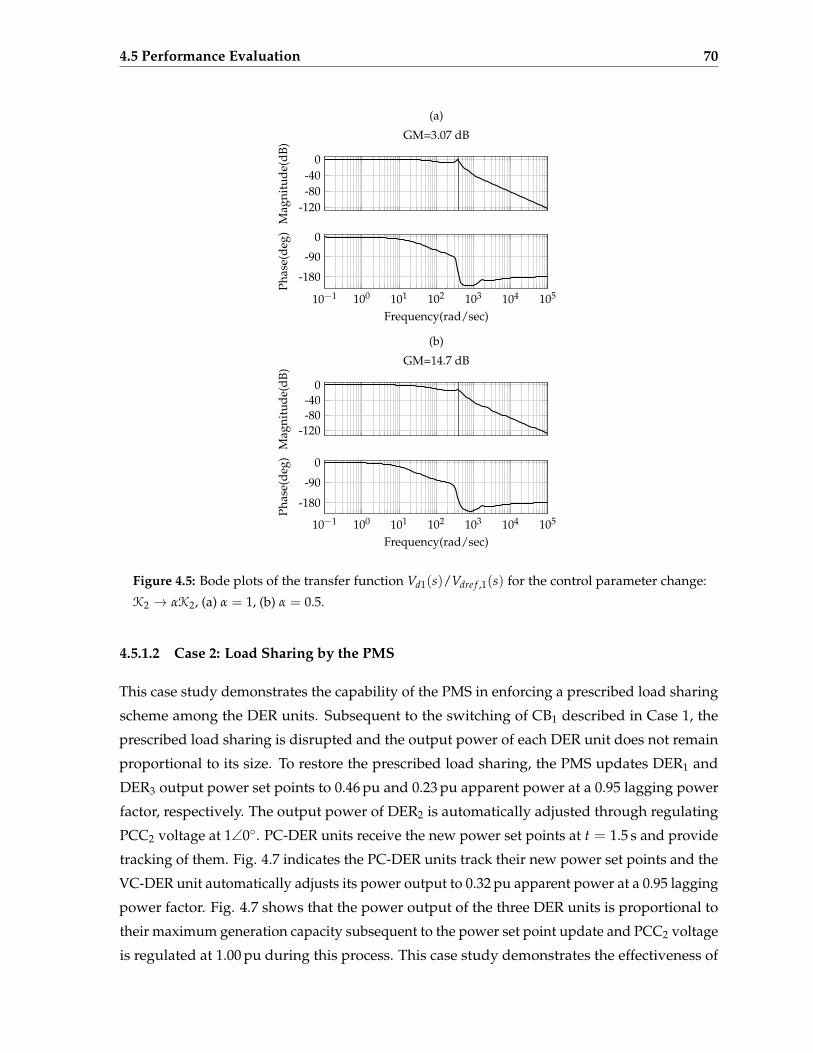
4.5 Performance Evaluation 70
0-40-80
-120
Mag
nitu
de(d
B)
(a)
GM=3.07 dB
10−1 100 101 102 103 104 105
0
-90
-180
Frequency(rad/sec)
Phas
e(de
g)
0-40-80
-120
Mag
nitu
de(d
B)
(b)
GM=14.7 dB
10−1 100 101 102 103 104 105
0
-90
-180
Frequency(rad/sec)
Phas
e(de
g)
Figure 4.5: Bode plots of the transfer function Vd1(s)/Vdre f ,1(s) for the control parameter change:
K2 → αK2, (a) α = 1, (b) α = 0.5.
4.5.1.2 Case 2: Load Sharing by the PMS
This case study demonstrates the capability of the PMS in enforcing a prescribed load sharing
scheme among the DER units. Subsequent to the switching of CB1 described in Case 1, the
prescribed load sharing is disrupted and the output power of each DER unit does not remain
proportional to its size. To restore the prescribed load sharing, the PMS updates DER1 and
DER3 output power set points to 0.46 pu and 0.23 pu apparent power at a 0.95 lagging power
factor, respectively. The output power of DER2 is automatically adjusted through regulating
PCC2 voltage at 1∠0. PC-DER units receive the new power set points at t = 1.5 s and provide
tracking of them. Fig. 4.7 indicates the PC-DER units track their new power set points and the
VC-DER unit automatically adjusts its power output to 0.32 pu apparent power at a 0.95 lagging
power factor. Fig. 4.7 shows that the power output of the three DER units is proportional to
their maximum generation capacity subsequent to the power set point update and PCC2 voltage
is regulated at 1.00 pu during this process. This case study demonstrates the effectiveness of

4.5 Performance Evaluation 71
−1
0
1
V2,
abc(p
u)
(a)
0
0.5
1
P,Q
DG
,1(p
u)
(b)
0
0.5
1
P,Q
DG
,2(p
u)
(c)
0.75 0.8 0.85 0.9
0
0.5
1
P,Q
DG
,3(p
u)
(d)
Time(s)
Figure 4.6: Microgrid transients due to CB1 opening: (a) PCC2 voltage, (b)–(d) real/reactive output
power of the three DER units, P: Q: .
the proposed power management scheme in enforcing the load sharing scheme.
4.5.1.3 Case 3: DER2 Overload Protection
The objective of this case study is to demonstrate the necessity and performance of the overload
protection scheme of Section 3.4 when the VC-DER is subject to an overload. Subsequent to
the power set point update of Case 2, CB1 which was opened in Case 1, is closed at t = 3 s. Fig.
4.8 shows that since the low output power of the PC-DER units cannot be changed without
a command from the PMS, DER2 undertakes supplying the increased power demand of the
microgrid. However, since it reaches its maximum generation capacity, the overload protection
scheme is triggered and limits the apparent output power of DER2 to its maximum capacity of
0.75 pu, Fig. 4.8(c). Since the three DER units fail to meet microgrid net load demand, and the
voltage controller of the VC-DER is disabled to limit its output power, PCC2 voltage drops to
0.90 pu, Fig. 4.8(a). Fig. 4.8(b) and (d) shows that the output power of the PC-DER units remain
unchanged during this process. This case study demonstrates that the proposed overload
protection scheme for the VC-DER unit, which inherently lacks a power limiting capability, can
effectively limit the output power in case of overloading conditions.
To restore the voltage of the system and the prescribed load sharing scheme, the PMS
updates power set points for the PC-DER units to increase their output power. The new set
points of the PMS balance the power demand and generation of the microgrid and restore the

4.5 Performance Evaluation 72
−1
0
1
V2,
abc(p
u)
(a)
0
0.5
1
P,Q
DG
,1(p
u)
(b)
0
0.5
1
P,Q
DG
,2(p
u)
(c)
1.45 1.5 1.55 1.6
0
0.5
1
P,Q
DG
,3(p
u)
(d)
Time(s)
Figure 4.7: Achieving a prescribed load sharing scheme by the PMS: (a) PCC2 voltage, (b)–(d)
real/reactive output power of the three DER units, P: Q: .
voltage to 1.00 pu, Fig. 4.9(a). Fig. 4.9(b)–(d) shows that, subsequent to this power set point
update, microgrid operating condition will be restored to that of Case 1, prior to the switching
of CB1.
4.5.2 Hardware-in-the-loop Simulation Test Case
This section presents the results of real-time simulation of the proposed control strategy based
on the HIL concept. The objective of this study is to verify that the proposed scheme can be
digitally implemented in an industrial hardware platform despite hardware implementation
issues. Real-time simulation setup, equipment, and component models are the same as those of
Section 2.8.2.
4.5.2.1 Case 4: Induction Motor Energization
To verify the performance of the proposed control strategy, an induction motor energization
test case is carried out while the controllers are implemented in the HIL environment. This
case study demonstrates the robustness of LCs when the microgrid is subject to a motor
energization, which is a nonlinear, time-varying disturbance. Prior to motor start-up, the
three DER units deliver 0.75 pu(0.25 pu), 0.22 pu(0.19 pu), and 0.44 pu(0.19 pu) real(reactive)
power. Three induction motors are simultaneously connected to the bus labeled as Bm in Fig.

4.6 Conclusions 73
−1
0
1
V2,
abc(p
u)
(a)
0
0.5
1
P,Q
DG
,1(p
u)
(b)
0
0.5
1
P,Q
,S DG
,2(p
u)
(c)
1.95 2 2.05 2.1 2.15 2.2
0
0.5
1
P,Q
DG
,3(p
u)
(d)
Time(s)
Figure 4.8: Overloading protection: (a) PCC2 voltage, (b)–(d) apparent/real/reactive output power
of the three DER units, P: Q: S: .
4.1(a) through a Yg/∆, 13.8 kV/0.4 kV step-down transformer. Three motors are energized
simultaneously to evaluate the control performance for the most severe disturbance while the
inrush currents of the motors do not exceed DER unit ratings and realistic motor parameters are
used. Motor parameters are given in Table 4.3. The resultant DER unit transients are illustrated
in Fig. 4.10, which shows the output power of PC-DER units remain unchanged. To maintain
PCC2 voltage at 1.00 pu, DER2 increases its real(reactive) output power to 0.46 pu(0.30 pu)
in response to motor energization transients. This case study shows that although LCs are
designed based on an LTI model of the system, their robust performance is ensured even
for microgrid time-varying uncertainties, i.e., an induction motor energization in this case.
Induction machine energization is generally considered a severe disturbance and has been
reported to cause microgrid instability [20]. However, the proposed generalized microgrid
control strategy is able to reject such a disturbance due to its robustness.
4.6 Conclusions
This chapter presents a generalized power management and control strategy for an autonomous,
multi-DER microgrid. The envisioned strategy designates DER units as power-controlled and
voltage-controlled and assumes no dominant DER unit. It provides (i) power management for
the overall microgrid, (ii) an open-loop frequency control and synchronization, and (iii) a local,

4.6 Conclusions 74
−1
0
1
V2,
abc(p
u)
(a)
0
0.5
1
P,Q
DG
,1(p
u)
(b)
0
0.5
1
P,Q
,S DG
,2(p
u)
(c)
2.9 2.95 3 3.05 3.1 3.15 3.2 3.25 3.3
0
0.5
1
P,Q
DG
,3(p
u)
(d)
Time(s)
Figure 4.9: Resolving the overload condition by assigning new power set points for PC-DER units:
(a) PCC2 voltage, (b)–(d) apparent/real/reactive output power of the three DER units, P: Q:
S: .
robust, decentralized controller for each DER unit. The power management system determines
output power set points for the PC-DER units and a voltage set point for the VC-DER unit
to enforce a prescribed load sharing scheme among the DER units and regulate the overall
microgrid voltage profile within a permissible range. Frequency of the system is controlled in an
open-loop manner by utilizing an internal crystal oscillator for each DER unit that also generates
the angle waveform required for dq/abc (abc/dq) transformations. Synchronization of DER
units is achieved by exploiting a GPS-based common time-reference signal. The local control
of each DER unit is designed based on a new multivariable decentralized robust controller
approach which utilizes a linear state-space model of the microgrid. Eigenanalysis shows that
the closed-loop system is stable and well-damped and the controllers are apropriately designed.
The controller parameter range of variations that result in a stable closed-loop system are
reported and the relationship between controller robustness and its parameters are determined.
The reported results are obtained from (i) time-domain simulation studies in the PSCAD/-
EMTDC platform, and (ii) an RTDS-based hardware-in-the-loop environment. Various sim-
ulation studies validate the desired performance of the microgrid. The test cases in the HIL
environment are based on digital implementation of the controller of each DER unit in an
NI-cRIO industrial control platform and verify (i) ease of hardware realization of the proposed
power management and DER controller, (ii) lack of sensitivity to hardware environment issues.

4.6 Conclusions 75
Table 4.3
NUMERICAL PARAMETERS OF THE INDUCTION MACHINES
Rated Power 180 hp
Rated Voltage 0.4 kV
Rotor H Constant 0.6 s
Stator Resistance 0.0425 pu
Stator Leakage Inductance 0.0870 pu
First Rotor Resistance 0.0300 pu
First Rotor Leakage Inductance 0.0658 pu
Second Rotor Resistance 0.0500 pu
Second Rotor Leakage Inductance 0.0739 pu
Magnetizing Inductance 2.97 pu
Figure 4.10: Microgrid transients due to simultaneous energization of three induction motors.

5 Smooth Microgrid
Control Transition
5.1 Introduction
CHAPTER 2 introduced a voltage control scheme for an islanded multi-DER microgrid.
The control method is also required to perform satisfactorily under the following two
circumstances:
1. Transition to an islanded mode of operation: In the grid-connected mode of operation, mi-
crogrid voltage is predominantly dictated by the main grid and DER units control their
output real/reactive power components. This is achieved based on the well-established
inner current control loop [82] which is briefly described in Appendix B. Should a transi-
tion to an islanded mode of operation occur, due to either a disturbance in the main grid or
other considerations, the microgrid control should switch from the power tracking mode
to the voltage tracking mode to regulate microgrid voltage profile within the permissible
range.
2. Communication failure: The microgrid voltage control scheme relies on a low-bandwidth
communication link for 1) synchronizing the DER units and 2) communicating set points
from the power management system (PMS) to local controllers (LCs). Loss of neither
of these communication signals will cause immediate microgrid instability. However,
if communication failure lasts long enough so that DER units step out of synchroniza-
tion due to the oscillator inaccuracy or significant microgrid operating point changes,
instability issues can arise. Hence there is a need for a backup control scheme in case of
communication failure.
In the above two cases, there is a need to switch from an “active” to a “latent” controller.
In Case 1, the active (latent) controller tracks DER output power (the corresponding PCC
voltage). In Case 2, the active (latent) controller is the voltage controller (a droop-based backup

5.2 Transition to Islanded Mode of Operation 77
controller). This transition should be performed smoothly while a “bumpless” control signal
is retained [80], otherwise the closed-loop system may experience transients that can result
in protection system activation and/or instability. This chapter proposes smooth transition
schemes for the above two scenarios and verifies the effectiveness of the proposed schemes
based on simulation case studies.
5.2 Transition to Islanded Mode of Operation
The existing microgrid control methods can be categorized based on employing 1) the same
control scheme for both grid-connected and islanded modes of operation [23, 83], and 2) two
different controllers one corresponding to each mode of operation. The latter needs various
methods to minimize the transients, e.g., use of communication [43], a special PLL design [84],
admittance compensation [85], and indirect current control [86]. In this section, we propose
a new observer-based method. The focus is on the transition from the grid-connected to the
islanded mode since it can accompany severe transients and consequently result in instability,
especially when a significant amount of power is exchanged between the main grid and the
microgrid immediately prior to the transition. To minimize the transients due to the switching
between the two controllers corresponding to the two modes of operation, a smooth control
signal should be retained prior and subsequent to the transition, i.e., u1(t−SW) = u2(t+SW), where
tSW is the instant of switching between the grid-connected mode and the islanded mode control
schemes, and u1 and u2 are the active and the latent control outputs, respectively. Smooth
transition can be achieved by appropriately initializing the voltage controller state variables.
Since the controller states are available owing to its digital implementation, an observer-based
method is proposed.
5.2.1 Smooth Transition Scheme Based on a State Observer
In the grid-connected mode of operation, DER units control their output real/reactive power
components based on the approach described in Appendix B. In the islanded mode of operation,
DER units control their PCC voltages. Each DER LC can be described by Fig. 5.1, based on the
control method introduced in Chapter 2. In the schematic diagram of Fig. 5.1, the measured
PCC voltage is transformed to a dq frame of reference and compared with voltage set points,
then the control action is performed and necessary VSC switching signals are generated to
track the set points. To provide a smooth transition from the power controller, Appendix B, to
the voltage controller of Fig. 5.1, the control signal should remain continuous at the instant of
switching, i.e., Vtd1(t−SW) = Vtd2(t+SW) and Vtq1(t−SW) = Vtq2(t+SW), Fig. 5.2. To achieve this, the
voltage controller is augmented with a state observer (or estimator) to properly initialize its

5.2 Transition to Islanded Mode of Operation 78
abc/dq x = Acx + Bcu
y = Ccx + Dcu
Controller
dq/abcPWM Signal
Generator
Oscillator
vabc†
Vdq,re f
‡ ¶θ
†: Vdq
‡: Vt,dq
¶: vt,abc
Figure 5.1: A block diagram of the voltage control scheme.
state variables. The observer is designed based on the state-space parameters of the voltage
controller, Ac, Bc, Cc, Dc, as specified in Fig. 5.1. The observer inputs are the outputs of the
current controller, and the measured PCC voltage and reference set points, Fig. 5.2. The output
of the observer is the state vector x that determines the initial conditions of the state variables
of the voltage controller. To further reduce transients, the voltage reference set points of the
voltage controller are selected to be equal to the measured PCC voltage.
Each observer is designed based on the Kalman estimation process [87] and is of the form
˙x = Ao x + Bou,
yobs = x,(5.1)
where x is the estimated state variable, u =[Vd, Vq, Vd,re f , Vq,re f , Vtd1, Vtq1
]T, yobs is the output of
the observer which is equal to the estimated states, and F and G are the outputs of the Kalman
estimation process.
5.2.2 Performance Evaluation
To verify performance of the proposed smooth transition scheme from the grid-connected
mode controllers to islanded mode controllers, two simulation case studies in PSCAD/EMTDC
platform are conducted. Component models and parameters are the same as those of Chapter 2.
Each observers is designed using the kalman function of Matlab Control Toolbox [87], discritized
with a sampling rate of 6 kHz, coded in FORTRAN, and embedded in the FORTRAN code of
voltage controllers. The observer design process is performed for each LC and the following Fi
and Gi, corresponding to LCi, i = 1, 2, 3, are obtained:
Ao1 =
0.73 −0.40 −0.66
0.01 0.90 0.05
0.02 −0.05 0.99
, B1 =
−20.16 127.11 0.20 0.33 0.38 −3.37
−7.81 −2.83 −0.95 −0.02 −0.52 −0.05
−3.53 −10.45 0.02 −0.99 −0.14 −0.14
,

5.2 Transition to Islanded Mode of Operation 79
Voltage
Controller
Vtd2
Vtq2
VdVq
Vd,re fVq,re f
Observer
Current
Set Point
Calcu-
lation
Id,re f
Iq,re f
VdVq
Pre fQre f
Current
Controller
Vtd1
Vtq1
x
Latent Controller
Active Controller
Figure 5.2: The proposed observer-based smooth transition scheme.
Ao2 =
0.74 −0.46 −0.65
0.01 0.95 0.00
0.01 0.09 0.91
, B2 =
−25.31 119.71 0.23 0.32 0.11 −3.48
−2.59 −6.47 −0.97 −0.01 −0.18 −0.08
9.20 −7.73 −0.04 −0.95 0.61 −0.08
,
Ao3 =
0.74 −0.46 −0.65
0.01 0.95 0.00
0.01 0.09 0.91
, B3 =
−25.31 119.71 0.23 0.32 0.11 −3.48
−2.59 −6.47 −0.97 −0.00 −0.18 −0.08
9.20 −7.73 −0.04 −0.95 0.61 −0.08
.
5.2.2.1 Planned Islanding
Initially, the microgrid is importing 0.28/0.39 pu real/reactive power from the main grid which
is a significant amount of power mismatch and can cause transients and potentially instability
issues, if necessary measures are not taken before islanding. The three DER units deliver
0.56/0.00, 0.69/0.13, and 0.38/0.00 pu real/reactive power, respectively, and Line1(Line2) trans-
fers 0.42(0.00)pu real power. At t = 1 s, CBg is opened and the microgrid is expected to
continue its operation in the islanded mode. After the switching event, the three DER units de-
liver 0.68/0.09, 0.79/0.41, and 0.44/0.63 pu real/reactive power, respectively, and Line1(Line2)
transfers −0.15(−0.10)pu real power. The resultant microgrid transients for the case that the

5.2 Transition to Islanded Mode of Operation 80
−1
0
1V
1,ab
c(pu)
(a)
−1
0
1
P,Q
DE
R,1(p
u)
(b)
0.95 1 1.05 1.1 1.15 1.2
0.20.40.60.8
1
V1,
mag
(pu)
(c)
Time(s)
−1
0
1
V1,abc(pu)
(d)
−0.5
0
0.5
1
P,QDER,1(pu)
(e)
0.95 1 1.05 1.1 1.15 1.20.95
1
1.05
V1,mag(pu)
(f)
Time(s)
Figure 5.3: Planned islanding of the microgrid while the smooth transfer scheme is deactivated/in
service: (a) and (d) three-phase voltages of PCC1, (b) and (e) DER1 real/reactive output power, and
(c) and (f) magnitude of PCC1 voltage, P: Q: .
smooth transition scheme is not in service are illustrated in Fig. 5.3(a–c). Fig. 5.3(a) and (c)
shows that three-phase voltages of PCC1 are distorted and the voltage magnitude transiently
drops to 0.2 pu. Fig. 5.3(b) indicates that real/reactive output power components of DER1
exhibit excessive transients that can damage either the prime-mover or the power electronic
components of the DER unit. However, since the voltage controllers are highly robust, they
manage to bring the microgrid to a steady-state normal operating point.
The same study is repeated while the smooth transition scheme is in service and the results
are shown in Fig. 5.3(d–f). Fig. 5.3(d) and (f) show that PCC1 voltage is well regulated and
experiences insignificant transients. DER1 output power components also exhibit less severe
transient responses while the significant power exchange between the microgrid and the main
grid is abruptly interrupted due to the islanding event. Fig. 5.3 demonstrates the effectiveness
of the proposed smooth transition scheme.
5.2.2.2 Unintentional Islanding
The initial conditions of this case study are the same as those of the previous one. However, in
this case the islanding is due to a single-phase to ground fault which occurs at t = 0.95 s in the
main grid. The fault location is at a node which divides the impedance Rg + jXg, Fig. 2.1(a),
into two equal parts. 50 ms after the fault occurrence, CBg is opened to isolate the microgrid
from the faulty main grid. This switching event is communicated to LCs of DER units to switch

5.3 Control Transfer due to Communication Failure 81
−1
0
1
V1,
abc(p
u)
(a)
0.9 0.95 1 1.05 1.1 1.15−2
−1
0
1
P,Q
DE
R,1(p
u)
(b)
Time(s)
Figure 5.4: Unintentional islanding of the microgrid due to a fault in the main grid: (a) three-phase
voltages of PCC1, (b) DER1 real/reactive output power, P: Q: .
their modes of operation from the power tracking mode to the voltage tracking mode while the
smooth transition scheme is in service. Fig. 5.4 shows microgrid transients due to this sequence
of events. Fig. 5.4 indicates that although the microgrid is isolated under a severe disturbance,
1) a smooth transition is achieved and 2) the latent voltage controllers manage to restabilize the
microgrid and reach a new feasible steady-state operating condition. If the smooth transition
scheme were not in service, the excessive postfault transients exacerbated with control transfer
transients could trigger microgrid protection system and trip out DER units.
5.3 Control Transfer due to Communication Failure
Since the operation of voltage controllers of Chapter 2 depends on the availability of two
low-bandwidth communication links to 1) synchronize the DER units and 2) communicate
set points to local controllers, there is a need to provide a backup control scheme in case of
communication failure. Switching to the backup scheme is initiated depending on the type of
communication failure as described below:
• In case of communication failure of the DER synchronizing signals, which is considered
unlikely due to the reliability of the GPS system, the impacted local controller notifies
the PMS, Fig. 2.1(b), which in turn, notifies all local controllers to switch to the backup
control scheme.
• In case of communication failure associated with set point transmitting signals, the
impacted local controller switches to the backup scheme immediately and the PMS, that
has also detected the loss of communication, notifies the other two LCs to switch to the
backup control scheme.

5.3 Control Transfer due to Communication Failure 82
CA G
TL CL
PlantActive Controller
Auxiliary Tracking Controller Latent Controller
ruA
y
uLS
+
−
+
−+
+
+ −
Figure 5.5: Smooth control transfer scheme based on an auxiliary tracking controller.
A droop-based control (Appendix C) is adapted to operate as the backup control. This
section also proposes a smooth control transition scheme for transition between the voltage
controllers of Chapter 2 and the droop-based backup control scheme of Appendix C. The
reasons for introducing this smooth transition scheme, rather than using that of Section 5.2.1,
are the following:
• If states of the latent controller, i.e., the droop-based backup control, are not accessible or
modifiable, e.g., when the latent controller is analog, the observer-based smooth transition
scheme will not be applicable.
• This new scheme does not require an observer and thus simplifies its implementation
process.
This smooth control transition scheme uses an auxiliary controller and is described in the next
section.
5.3.1 Smooth Transition Based on an Auxiliary Controller
Fig. 5.5 illustrates a schematic diagram of the smooth transition scheme based on an auxiliary
controller. Initially, the system is in closed-loop condition while the active controller CA is
controlling the plant G and switch S is closed. In this case, the latent controller CL is considered
as a dynamical system whose output uL is forced to track the output of the active controller, uA.
The auxiliary tracking controller TL is used to use the output of the active controller as its set
point and make the latent controller generate the same output as the active controller. While uL
is tracking uA, smooth transition to the latent controller can be achieved by opening switch S
and eliminating the effect of the auxiliary controller TL.

5.3 Control Transfer due to Communication Failure 83
(a) (b)
1DP
12Hs
1s
KD
PI S/H
ωre f
ωPCC Pre f P
∠Vt,L
ωPCC
ω
∠Vt,A
∠Vt,L tSW
+
−+
+
−+
−
−+
+
+
−+
Latent Controller
Auxiliary Tracking Controller
DQ
PI S/H
Q
Es
|Vt,L|
|Vt,A|
|Vt,L| tSW
−+
+
−
Latent Controller
Auxiliary Tracking Controller
Figure 5.6: Droop-based backup control scheme that provides smooth transition, L: Latent, A:
Active.
Fig. 5.6 shows the modified droop-based backup control of Fig. C.2 which enables a smooth
control transition. The droop-based control of each DER unit includes two controllers: 1) the
controller of Fig. 5.6(a) which specifies the angle of VSC terminal voltage and 2) the controller
of Fig. 5.6(b) which specifies the amplitude of VSC terminal voltage. Thus, while the voltage
controllers are active, the angle and the amplitude of VSC terminal voltage, |Vt,A| and ∠Vt,A, are
measured and provided to the auxiliary PI controllers as highlighted by the bold lines in Fig. 5.6.
These auxiliary controllers force the backup droop-based controller to track the VSC terminal
voltage prior to control transfer instant. At the time of switching, tSW , the Sample/Hold
block is activated so that the outputs of the auxiliary PI controllers are frozen and the backup
droop-based controllers undertake control of the corresponding DER unit thereafter.
5.3.2 Performance Evaluation
To verify performance of the proposed smooth transition scheme based on the auxiliary con-
troller, two simulation case studies in PSCAD/ EMTDC platform are conducted. Component
models and parameters are the same as those of Chapter 2. The droop-based backup con-
trollers are augmented with the auxiliary tracking controllers and included in the simulation
model. Parameters of the droop-based backup control of Fig. 5.6 are H = 0.5 s, DP = 0.05 pu,
DQ = 0.05 pu, and KD = 30.

5.3 Control Transfer due to Communication Failure 84
0
1
2
V2,
mag
(pu)
(a)
0
1
2
3
P DE
R,i(p
u)
(b)
−4
−2
0
QD
ER
,i(pu)
(c)
2.95 3 3.05 3.1 3.15 3.250
100
150
f (H
z)
(d)
Time(s)
0.95
1
1.05
V2,
mag
(pu)
(e)
0.4
0.6
0.8
1
P DE
R,i(p
u)
(f)
0.1
0.2
0.3
QD
ER
,i(pu)
(g)
2.95 3 3.05 3.1 3.15 3.259.5
60
60.5
f (H
z)
(h)
Time(s)
Figure 5.7: Transfer to backup control while the smooth transition scheme is deactivated/in service:
(a) and (e) magnitude of PCC2 voltage, (b) and (f) DERi real output power, (c) and (g) DERi reactive
output power, (d) and (h) frequency of the microgrid, DER1: DER2: DER3: .
5.3.2.1 Simultaneous Transfer to Backup Controller
In this case study, transition from the main controllers to the backup controllers of the three DER
units occurs simultaneously. Initially, the microgrid is operating in an islanded mode based on
the voltage control scheme of Chapter 2 and the three DER units deliver 0.84/0.25, 0.64/0.19,
and 0.43/0.13 pu real/reactive power, respectively. Line1(Line2) transfers 0.00(0.13)pu real
power, respectively. At t = 3 s, due to a communication failure, the LCs are notified to switch
to the backup scheme. Microgrid transients due to this switching event are illustrated in Figs.
5.7(a)–(d)/5.7(e)–(h) when the smooth transition scheme is inactive/in service. In both cases,
subsequent to the control transfer, the same steady-state operating point is achieved. However,
Fig. 5.7 clearly reveals that the microgrid transient response is substantially improved due to
the proposed smooth control transition scheme.
5.3.2.2 Nonsimultaneous Transfer to Backup Controllers
Since the transfer to the backup controller occurs due to a communication failure, it may well
be the case that the three LCs are transferred to the backup scheme at different time instants.

5.4 Conclusions 85
0.95
1
1.05
V2,
mag
(pu)
(a)
0
0.5
1
P DE
R,i(p
u)
(b)
0
0.2
0.4Q
DE
R,i(p
u)(c)
3 3.2 3.4 3.6 3.8 4 4.259.5
60
60.5
f (H
z)
(d)
Time(s)
Figure 5.8: Nonsimultaneous transfer to backup control: (a) magnitude of PCC2 voltage, (b) and
(c) DERi real/reactive output power, and (d) frequency of the microgrid, DER1: DER2:
DER3: .
This case study illustrates the response of the closed-loop microgrid when the transfers are
not simultaneous. The pretransition operating point is the same as that of the previous case
study. At t = 3 s, a loss of communication is detected by LC2 and the backup controller is
activated immediately. LC1 and LC3 transfer to the backup scheme with 1 s and 0.5 s delays,
respectively. Fig. 5.8 shows microgrid transients due to this sequence of controller transfers.
Fig. 5.8 signifies that although the microgrid exhibits insignificant oscillatory dynamics due
to the transfer delays, it maintains stability and continues its normal operation after all LCs
switch to the backup scheme.
5.4 Conclusions
This chapter presents two microgrid smooth control transition schemes for the following two
scenarios:
1. In case of microgrid islanding, there is a need to transfer from the power-tracking to the
voltage-tracking controllers.
5.4 Conclusions 86
2. In case of communication failure, there is a need to transfer from the voltage controllers
to the backup droop-based controllers.
Controller transfer should be performed smoothly to avoid severe transients due to the
switching event. To achieve this, two different smooth control transition schemes based
on 1) an observer, and 2) an auxiliary tracking controller are proposed for the above two
scenarios, respectively. The observer-based method initializes states of the voltage controller
properly such that its outputs are identical to those of the power controller at the instant of
switching and thereby a smooth transition is achieved. The second scheme employs an auxiliary
tracking controller that makes the backup droop-based controller track the output of the voltage
controller so that at the switching time instant a bumpless control output is retained.
The performance of the proposed smooth transition schemes are verified based on time-
domain simulations. Results show that employing the proposed smooth transition schemes
substantially improves the transient response of the microgrid. In case of the observer-based
scheme, it was shown that subsequent to islanding, the microgrid continues its normal operation
smoothly, even when a significant power mismatch between the microgrid and the main grid
exists, and also when the transition occurs due to a fault in the main grid. This is mainly due
to the robustness of the voltage controllers and effectiveness of the smooth transition scheme.
In case of smooth transition to droop-based backup control, it was shown that the smooth
transition scheme responded as expected, even when the transfer instants of different DER
units are not simultaneous.

6 Conclusions
6.1 Summary & Conclusions
THIS dissertation proposes a power management and a control strategy for an islanded
microgrid that includes multiple electronically-interfaced DER units. The envisioned
strategy consists of
1. a microgrid power management system that, based on a classical power flow analysis,
determines the terminal voltage set points for DER units;
2. an open-loop frequency control and synchronization scheme that controls the frequency
of the system in an open-loop manner, by utilizing an internal crystal oscillator for each
DER unit, and synchronizes the DER units by exploiting a GPS-based time-reference
signal; and
3. a local, robust, decentralized controller for each DER unit which is designed taking a
novel multivariable robust decentralized servomechanism approach, based on a linear
state-space model of the microgrid.
The controller design procedure is outlined and various attributes of the controller, i.e., the
existence conditions, gain-margins, robustness, and tolerance to input delays are analytically
discussed. This control strategy is then generalized by considering both voltage-controlled and
power-controlled DER units and applied to a more elaborate microgrid system. Eigenvalue
sensitivity and robustness analyses are performed to study dynamic behavior of the closed-loop
system.
Since the proposed voltage control method lacks an inner current control loop, it subjects
the corresponding DER unit to overcurrent/overload conditions due to system severe distur-
bances, e.g., faults and switching events. Hence, this dissertation proposes control-imbedded
overcurrent and overload protection schemes to prevent DER unit from trip-out or damage in
case of faults and overload conditions. The proposed protection schemes detect the abnormal

6.1 Summary & Conclusions 88
condition, disable the main voltage controllers, and modify the terminal voltage of the interface
VSC to limit the output current and/or power of the DER unit within the permissible range.
This dissertation also devises smooth control transition schemes for 1) microgrid islanding,
and 2) communication failure events. These schemes operate based on 1) an observer and 2) an
auxiliary tracking controller, and are integrated with the microgrid active controllers to provide
a smooth control transition when switching to a latent controller is necessary.
The following qualitative and quantitative conclusions can be drawn from the dissertation.
6.1.1 Qualitative Conclusions
• A robust, decentralized control strategy is a viable solution for control of an islanded
microgrid since 1) a microgrid exhibits a high level of uncertainty and a robust controller
performs its satisfactory operation regardless of the uncertainties, and 2) time-varying
signals cannot be transmitted to a central control system due to communication limita-
tions and a decentralized controller obviates such a need and also facilitates unplanned
connection/disconnection of DER units.
• Eigenvalues and participation factor analysis indicates that the dominant poles of the
closed-loop system are predominantly influenced by controllers’ states and signifies the
appropriate design of the controllers thereby (Sections 2.6.1 and 4.4.1).
• Eigenvalue sensitivity analysis of the microgrid indicates that the closed-loop system
remains stable for practical perturbations of load parameters. However, reducing the
resistance and increasing the inductance/capacitance of loads result in a more oscillatory
system. Likewise, a larger (smaller) filter (distribution line) impedance renders the system
less damped (Section 2.6.2).
• Robustness analysis verifies the results obtained from eigenvalue sensitivity analysis
and also concludes that a higher control gain results in a faster control response while
reducing its robustness (Section 2.7.2 and 4.4.2).
• Offline time-domain simulations in PSCAD/EMTDC platform demonstrate the robust
performance of the controllers subject to various system disturbances, e.g., load change,
set point change, microgrid configuration variation, abrupt outage of DER units, and
even induction motor energization which exhibits a nonlinear and time-varying behavior
in the start-up phase. The simulation results also suggest that the proposed PMS can suc-
cessfully control the power flow of the microgrid and the proposed open-loop frequency
control and synchronization scheme maintains microgrid frequency irrespective of its
transients.
• Real-time HIL simulation studies, using an RTDS system and NI-cRIO industrial con-
trollers, validate offline time-domain simulation results, signify ease of hardware im-

6.1 Summary & Conclusions 89
plementation of the proposed control, and indicate control insensitivity to hardware
implementation issues, e.g., noise, PWM nonidealities, A/D and D/A conversion nonide-
alities, and descritization errors/delays.
• The proposed strategy can be generalized to cover both voltage-controlled and power-
controlled DER units to achieve an optimal operating condition.
• The overcurrent/overload protection schemes can effectively limit the DER unit output
current/power in case of faults and overloading conditions. Furthermore, an anti-windup
scheme can be used to minimize the controller restoration transients, subsequent to the
operation of the overcurrent/overload protection.
• The fault clearance determination scheme performs successfully for all types of faults,
including those that generate double-frequency oscillations in d and q components of the
PCC voltage.
• The observer-based smooth control transition scheme can effectively minimize the tran-
sients caused by control switching due to microgrid islanding. The smooth control
transition scheme, based on an auxiliary tracking controller, can effectively minimize
microgrid transients caused by switching from the main voltage controllers to the droop-
based backup controllers in case of communication failure. It was also observed that the
stability of the microgrid is preserved even if the backup controllers of DER units are not
activated simultaneously (Section 5.3.2.2).
6.1.2 Quantitative Conclusions
• Analysis of the closed-loop linearized microgrid dynamics reveals that the system has an
input/output gain margin of 1.28/1.38 which is quite satisfactory, and it is insensitive to
input delays of at least 1.58× 10⁻⁴ s.
• Robustness index of the closed-loop system (7.752× 10⁻²) is greater than that of the open-
loop system (1.495× 10⁻³), which signifies there is no deterioration in the robustness of
the system after augmenting the controllers.
• Eigenvalue sensitivity analysis determines the range of control parameter variations that
result in a stable closed-loop system (Sections 2.7.2 and 4.4.2).
• Offline time-domain simulation test cases conclude that controller settling time is less
than 50 ms and PCC voltages remain within the permissible range as defined by standards
and grid codes, in all case studies.
• The overcurrent protection scheme can limit the DER unit output current to about 1.2 pu
in the worst-case fault scenarios. In addition, the overload protection scheme can limit
the DER unit output power to its rated MVA under overloading conditions.
• The fault detection algorithm can rapidly detect fault conditions, e.g., within 200 µs

6.2 Contributions 90
(Section 3.5.2.1) and has the potential to be implemented in industrial protective relays
where speed is a major concern.
6.2 Contributions
The salient contributions of this thesis are as follows.
• It proposes i) a power management system to control the load sharing among DER units
by defining appropriate set ponits, ii) robust, decentralized DER local controllers to track
the specified set points and reject disturbances, and iii) an open-loop frequency control
and DER synchronization technique based on a time-reference signal received from a
GPS.
• An overcurrent protection scheme, including fault detection, current limitation, fault
clearance determination, and controller restoration processes, is suggested to prevent
trip-out or damage to DER units in case of faults. Moreover, an overload protection
scheme is proposed that limits the output power of the microgrid constituent DER units
within the permissible range.
The dissertation also
• introduces the notion of real stability radius, for the first time in the area of power systems,
to quantify control scheme robustness,
• integrates an anti-windup scheme with the overcurrent/overload protection algorithms,
which freezes/releases controller states when the main controller is disabled/in service,
to minimize microgrid transients subsequent to restoration of the main controllers,
• presents an observer-based smooth control transition scheme to minimize transients
caused by microgrid islanding, which is only applicable to controllers with modifiable
state variables, i.e., digital controllers,
• presents a smooth control transition scheme, based on an auxiliary tracking controller
to minimize transients caused by switching from the main to the droop-based backup
controllers. This scheme is applicable to controllers whose state variables are not accessi-
ble/modifiable, i.e., analog controllers.
6.3 Future Research Directions
Further research in continuation of this work includes the following:
• The power management system can be elaborated to include grid resynchronization,
state estimation, optimal power flow, unit commitment, contingency analysis, and data
mining functions.
6.3 Future Research Directions 91
• Source-side dynamics, i.e., dynamics of the DC-side of the interface VSC, have a secondary
effect on the AC-side and are not included in the reported studies. Future research
should therefore include source-side dynamics as well. Since DC-side modeling involves
nonlinearity, control development may necessitate using tools from nonlinear control
theory.
• The control system proposed in this dissertation does not actively compensate PCC
voltage imbalance and distortions caused by unbalanced and nonlinear loads. To en-
sure a balanced PCC voltage, it is suggested that robust decentralized controllers be
developed in the abc frame of reference to track sinusoidal reference signals and, as a
result, eliminate the imbalance. To ensure an acceptable total harmonic distortion of the
PCC voltage, controllers should include imaginary poles corresponding to significant
harmonic frequencies.
• It is suggested that the control strategy be modified for microgrid applications where
the DER units are nondispachable, e.g., wind and photovoltaic units. Integration of an
energy storage system, e.g., a battery bank, would be an option in this case to absorb
DER unit intermittency.
• It is also suggested that a microgrid protection scheme be devised and coordinated with
the proposed control and overcurrent/overload protection algorithms. In this case, some
level of interaction between the control and protection systems is anticipated that may
degrade microgrid performance and should be considered in the coordination procedure.

A Mathematical Model
Details
A.1 Equations in abc Frame
EQUATIONS describing the dynamics of Subsystem1 of Fig. 2.4 arei1,abc = it1,abc + C1
dv1,abcdt + iL1,abc +
v1,abcR1
,
vt1,abc = L f 1di1,abc
dt + R f 1i1,abc + v1,abc,
v1,abc = L1diL1,abc
dt + Rl1iL1,abc,
v1,abc = Lt1dit1,abc
dt + Rt1it1,abc + v2,abc,
(A.1)
and those of Subsystem2 and Subsystem3 arei2,abc = it2,abc + C2
dv2,abcdt + iL2,abc +
v2,abcR2
,
vt2,abc = L f 2di2,abc
dt + R f 2i2,abc + v2,abc,
v2,abc = L2diL2,abc
dt + Rl2iL2,abc,
v2,abc = Lt2dit2,abc
dt + Rt2it2,abc + v3,abc,
(A.2)
and i3,abc = it3,abc + C3
dv3,abcdt + iL3,abc +
v3,abcR3
,
vt3,abc = L f 3di3,abc
dt + R f 3i3,abc + v3,abc,
v3,abc = L3diL3,abc
dt + Rl3iL3,abc.
(A.3)
A.2 Equations in dq Frame
The above equations are then transformed to a dq frame of reference, yielding the following:
Subsystem1:
dV1,dqdt = 1
C1I1,dq − 1
C1It1,dq − 1
C1IL1,dq − 1
R1C1V1,dq − jωV1,dq,
dI1,dqdt = 1
L f 1Vt1,dq −
R f 1L f 1
I1,dq − 1L f 1
V1,dq − jωI1,dq,dIL1,dq
dt = 1L1
V1,dq − Rl1L1
IL1,dq − jωIL1,dq,dIt1,dq
dt = 1Lt1
V1,dq − Rt1Lt1
It1,dq − 1Lt1
V2,dq − jωIt1,dq.
(A.4)

A.3 State-space Equations 93
Subsystem2:
dV2,dqdt = 1
C2I2,dq − 1
C2It2,dq − 1
C2IL2,dq − 1
R2C2V2,dq − jωV2,dq,
dI2,dqdt = 1
L f 2Vt2,dq −
R f 2L f 2
I2,dq − 1L f 2
V2,dq − jωI2,dq,dIL2,dq
dt = 1L2
V2,dq − Rl2L2
IL2,dq − jωIL2,dq,dIt2,dq
dt = 1Lt2
V2,dq − Rt2Lt2
It2,dq − 1Lt2
V3,dq − jωIt2,dq.
(A.5)
Subsystem3:
dV3,dq
dt = 1C3
I3,dq − 1C3
It3,dq − 1C3
IL3,dq − 1R3C3
V3,dq − jωV3,dq,dI3,dq
dt = 1L f 3
Vt3,dq −R f 3L f 3
I3,dq − 1L f 3
V3,dq − jωI3,dq,dIL3,dq
dt = 1L3
V3,dq − Rl3L3
IL3,dq − jωIL3,dq.
(A.6)
A.3 State-space Equations
The above equations are used to construct the state-space model of the overall system
x = Ax + Bu,
y = Cx,(A.7)
where
xT =(V1,d, V1,q, I1,d, I1,q, IL1,d, IL1,q, It1,d, It1,q, V2,d, V2,q, I2,d, I2,q, IL2,d, IL2,q, It2,d, It2,q,
V3,d, V3,q, I3,d, I3,q, IL3,d, IL3,q),
uT =(Vt1,d, Vt1,q, Vt2,d, Vt2,q, Vt3,d, Vt3,q
),
yT =(V1,d, V1,q, V2,d, V2,q, V3,d, V3,q
),
and the A-matrix of (A.7), A ∈ R22×22, is A = blockdiagA1, A2, A3 where
A1 =
−1R1 C1
−ω 1C1
0 −1C1
0 −1C1
0
−ω −1R1 C1
0 1C1
0 −1C1
0 −1C1
−1L f 1
0 −R f 1L f 1
ω 0 0 0 0
0 −1L f 1
−ω−R f 1L f 1
0 0 0 01L1
0 0 0 −Rl1L1
−ω 0 0
0 1L1
0 0 −ω −Rl1L1
0 01
Lt10 0 0 0 0 −Rt1
Lt1−ω
0 1Lt1
0 0 0 0 −ω −Rt1Lt1
,
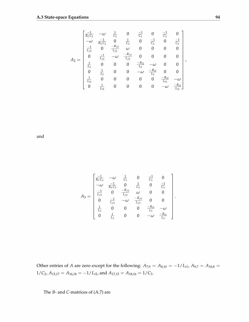
A.3 State-space Equations 94
A2 =
−1R2 C2
−ω 1C2
0 −1C2
0 −1C2
0
−ω −1R2 C2
0 1C2
0 −1C2
0 −1C2
−1L f 2
0 −R f 2L f 2
ω 0 0 0 0
0 −1L f 2
−ω−R f 2L f 2
0 0 0 01L2
0 0 0 −Rl2L2
−ω 0 0
0 1L2
0 0 −ω −Rl2L2
0 01
Lt20 0 0 0 0 −Rt2
Lt2−ω
0 1Lt2
0 0 0 0 −ω −Rt2Lt2
,
and
A3 =
−1R3 C3
−ω 1C3
0 −1C3
0
−ω −1R3 C3
0 1C3
0 −1C3
−1L f 3
0 −R f 3L f 3
ω 0 0
0 −1L f 3
−ω−R f 3L f 3
0 01L3
0 0 0 −Rl3L3
−ω
0 1L3
0 0 −ω −Rl3L3
.
Other entries of A are zero except for the following: A7,9 = A8,10 = −1/Lt1, A9,7 = A10,8 =
1/C2, A15,17 = A16,18 = −1/Lt2, and A17,15 = A18,16 = 1/C3.
The B- and C-matrices of (A.7) are

A.4 Mathematical Model of the Microgrid of Fig. 4.1 95
B =
0 0 0 0 0 00 0 0 0 0 0
1/L f 1 0 0 0 0 0
0 1/L f 1 0 0 0 0
0 0 0 0 0 00 0 0 0 0 00 0 0 0 0 00 0 0 0 0 00 0 0 0 0 00 0 0 0 0 00 0 1/L f 2 0 0 0
0 0 0 1/L f 2 0 0
0 0 0 0 0 00 0 0 0 0 00 0 0 0 0 00 0 0 0 0 00 0 0 0 0 00 0 0 0 0 00 0 0 0 1/L f 3 0
0 0 0 0 0 1/L f 3
0 0 0 0 0 00 0 0 0 0 0
,
and
C =
1 0 0 0 0 0 0 0 0 0 0 0 0 0 0 0 0 0 0 0 0 00 1 0 0 0 0 0 0 0 0 0 0 0 0 0 0 0 0 0 0 0 00 0 0 0 0 0 0 0 1 0 0 0 0 0 0 0 0 0 0 0 0 00 0 0 0 0 0 0 0 0 1 0 0 0 0 0 0 0 0 0 0 0 00 0 0 0 0 0 0 0 0 0 0 0 0 0 0 0 1 0 0 0 0 00 0 0 0 0 0 0 0 0 0 0 0 0 0 0 0 0 1 0 0 0 0
.
The above matrices are partitioned to identify blocks corresponding to each subsystem.
A.4 Mathematical Model of the Microgrid of Fig. 4.1
Mathematical model of the microgrid of Fig. 4.1, Chapter 4, is the same as the above model
except for the following: yT =(
I1,d, I1,q, V2,d, V2,q, I3,d, I3,q), yi = (Ii,d, Ii,q), i = 1, 3, and the

A.4 Mathematical Model of the Microgrid of Fig. 4.1 96
output matrix C should be replaced with C′ where
C′ =
0 0 1 0 0 0 0 0 0 0 0 0 0 0 0 0 0 0 0 0 0 00 0 0 1 0 0 0 0 0 0 0 0 0 0 0 0 0 0 0 0 0 00 0 0 0 0 0 0 0 1 0 0 0 0 0 0 0 0 0 0 0 0 00 0 0 0 0 0 0 0 0 1 0 0 0 0 0 0 0 0 0 0 0 00 0 0 0 0 0 0 0 0 0 0 0 0 0 0 0 0 0 1 0 0 00 0 0 0 0 0 0 0 0 0 0 0 0 0 0 0 0 0 0 1 0 0
.

B Output Power Control
ASINGLE-LINE block diagram of a VSC-interfaced DER unit is illustrated in Fig. B.1(a).
This appendix describes how the DER unit controls its output real/reactive power com-
ponents in grid-connected mode of operation. To achieve this, the well-established inner current
control loop of Fig. B.1(b) [82] is used. The set points for real/reactive power components are
translated into the set points for the d and q components of DER unit output current by
Id,re f =23
(VdPre f + VqQre f
V2d + V2
q
),
Iq,re f =23
(VqPre f −VdQre f
V2d + V2
q
),
(B.1)
where Vd and Vq are the d and q components of the PCC voltage. Current set points are then
fed into the current control loop of Fig. B.1(b) which provides tracking of these set points and
indirectly controls the output real/reactive power of the DER unit at the PCC.
(a) (b)
Vdc
DER UnitVt
jX
I
R
PCC
V
PI
PI
dq/abcSwitching
Signal
Generator
Vtd
Vtq
Id,re f
Iq,re f
Id
Iq
Vd
IqX
Vq
IdX
vt,abc
+
−
+
−
++
−
++
+
Figure B.1: (a) Schematic diagram of a DER unit, (b) block diagram of the current control loop.

C Droop Control
THIS appendix describes the droop-based control of [15] which is used as the backup
scheme in Chapter 5. The configuration of the DER unit is first explained and then
the frequency/real power ( f /P) and voltage/reactive power (V/Q) droop-based controls are
described.
C.1 DER Unit Configuration
Fig. C.1 illustrates a DER unit, represented by a dc voltage source, a voltage-sourced converter
(VSC), and a series RL filter, which is interfaced to the microgrid at the point of common
coupling (PCC in Fig. C.1) through a step-up transformer. The DER unit is interfaced to the
remainder of the microgrid at the PCC.
C.2 Frequency Control
This control scheme is analogous to that of a synchronous machine. A virtual inertia constant
H for the VSC unit of Fig. C.1 is assumed such that angular frequency of the voltage of the VSC
terminal, ω, is governed by
2Hdω
dt= Pm − Pout (C.1)
Vdc
DER UnitVt
jX
I
R
PCC
VMicrogrid
Remainder
Figure C.1: Schematic diagram a DER unit which is interfaced to the remainder of microgrid at the
PCC.

C.3 Voltage Control 99
(a) (b)
1DP
12Hs
1s
KD
ωre f
ωPCC Pre f P
δ
ωPCC
ω
+
−+
+
−+
−
−+
DQQ
Vt,re f
Vt−+
Figure C.2: Block diagram of the (a) f /P and (b) V/Q droop-based control.
where Pout is the DER unit output power at the PCC and Pm is the DER unit input power. Pm is
expressed as a droop function of system angular frequency by
Pm − Pre f =1
DP(ωre f −ωPCC), (C.2)
where ωPCC is the angular frequency of PCC voltage, DP is the f /P droop coefficient, and ωre f
and Pre f are reference set points for the PCC voltage angular frequency and DER output real
power. Augmenting the term corresponding to the viscous damping of the rotating shaft of a
synchronous machine with (C.1) results in the following
2Hdω
dt= Pm − Pout − KD(ω−ωPCC), (C.3)
where KD is the damping constant. The VSC terminal voltage angular frequency ω and phase-
angle δ are related based ondδ
dt= ω. (C.4)
The frequency control developed above is represented by the block diagram of Fig. C.2.
C.3 Voltage Control
The voltage controller of the DER unit of Fig. C.1 is based on V/Q droop characteristic given
by
Vt = Vt,re f − DQQ, (C.5)
where Q is the measured DER unit output reactive power, DQ is the V/Q droop coefficient,
and Vt,re f is the reference value of the VSC terminal voltage.

References
[1] R. A. Walling, R. Saint, R. C. Dugan, J. Burke, and L. A. Kojovic, “Summary of distributed
resources impact on power delivery systems,” IEEE Trans. Power Del., vol. 23, no. 3, pp.
1636–1644, Jul. 2008.
[2] R. H. Lasseter, “Microgrids,” in Proc. IEEE Power Engineering Society Winter Meeting, vol. 1,
2002, pp. 305–308.
[3] R. H. Lasseter and P. Piagi, “Microgrid: a conceptual solution,” in Proc. IEEE 35th Annual
Power Electronics Specialists Conf. PESC 04, vol. 6, Jun. 2004, pp. 4285–4290.
[4] N. Hatziargyriou, H. Asano, R. Iravani, and C. Marnay, “Microgrids,” IEEE Power Energy
Mag., vol. 5, no. 4, pp. 78–94, Jul./Aug. 2007.
[5] “DOE microgrid workshop report,” Office of Electricity Delivery and Energy Reliability,
Smart Grid R&D Program, San Diego, California, Tech. Rep., Aug. 2011.
[6] F. Katiraei, R. Iravani, N. Hatziargyriou, and A. Dimeas, “Microgrids management,” IEEE
Power Energy Mag., vol. 6, no. 3, pp. 54–65, May/Jun. 2008.
[7] IEEE Standard for Interconnecting Distributed Resources With Electric Power Systems, IEEE Std.
1547, 2003.
[8] IEEE Guide for Design, Operation, and Integration of Distributed Resource Island Systems with
Electric Power Systems, IEEE Std. 1547.4, 2011.
[9] F. Katiraei, “Dynamic analysis and control of distributed energy resources in a micro-grid,”
Ph.D. dissertation, University of Toronto, 2005.
[10] M. C. Chandorkar, D. M. Divan, and R. Adapa, “Control of parallel connected inverters in
standalone ac supply systems,” IEEE Trans. Ind. Appl., vol. 29, no. 1, pp. 136–143, Jan./Feb.
1993.

REFERENCES 101
[11] K. De Brabandere, B. Bolsens, J. Van den Keybus, A. Woyte, J. Driesen, and R. Belmans,
“A voltage and frequency droop control method for parallel inverters,” IEEE Trans. Power
Electron., vol. 22, no. 4, pp. 1107–1115, Jul. 2007.
[12] C. K. Sao and P. W. Lehn, “Autonomous load sharing of voltage source converters,” IEEE
Trans. Power Del., vol. 20, no. 2, pp. 1009–1016, Apr. 2005.
[13] P. Piagi and R. H. Lasseter, “Autonomous control of microgrids,” in Proc. IEEE Power
Engineering Society General Meeting, 2006.
[14] F. Katiraei, R. Iravani, and P. W. Lehn, “Micro-grid autonomous operation during and
subsequent to islanding process,” IEEE Trans. Power Del., vol. 20, no. 1, pp. 248–257, Jan.
2005.
[15] F. Gao and R. Iravani, “A control strategy for a distributed generation unit in grid-
connected and autonomous modes of operation,” IEEE Trans. Power Del., vol. 23, no. 2, pp.
850–859, Apr. 2008.
[16] Y. Li, D. M. Vilathgamuwa, and P. C. Loh, “Design, analysis, and real-time testing of a
controller for multibus microgrid system,” IEEE Trans. Power Electron., vol. 19, no. 5, pp.
1195–1204, Sep. 2004.
[17] H. Nikkhajoei and R. H. Lasseter, “Distributed generation interface to the CERTS micro-
grid,” IEEE Trans. Power Del., vol. 24, no. 3, pp. 1598–1608, Jul. 2009.
[18] C. K. Sao and P. W. Lehn, “Control and power management of converter fed microgrids,”
IEEE Trans. Power Syst., vol. 23, no. 3, pp. 1088–1098, Apr. 2008.
[19] T. L. Vandoorn, B. Meersman, L. Degroote, B. Renders, and L. Vandevelde, “A control
strategy for islanded microgrids with DC-link voltage control,” IEEE Trans. Power Del.,
vol. 26, no. 2, pp. 703–713, Apr. 2011.
[20] M. B. Delghavi and A. Yazdani, “An adaptive feedforward compensation for stability
enhancement in droop-controlled inverter-based microgrids,” IEEE Trans. Power Del.,
vol. 26, no. 3, pp. 1764–1773, Jul. 2011.
[21] J. M. Guerrero, J. C. Vasquez, J. Matas, L. G. de Vicuna, and M. Castilla, “Hierarchical
control of droop-controlled AC and DC microgrids—A general approach toward standard-
ization,” IEEE Trans. Ind. Electron., vol. 58, no. 1, pp. 158–172, Jan. 2011.
[22] X. Yu, A. M. Khambadkone, H. Wang, and S. Terence, “Control of parallel-connected
power converters for low-voltage microgrid—Part I: A hybrid control architecture,” IEEE
Trans. Power Electron., vol. 25, no. 12, pp. 2962–2970, Dec. 2010.

REFERENCES 102
[23] J. Kim, J. M. Guerrero, P. Rodriguez, R. Teodorescu, and K. Nam, “Mode adaptive droop
control with virtual output impedances for an inverter-based flexible AC microgrid,” IEEE
Trans. Power Electron., vol. 26, no. 3, pp. 689–701, Mar. 2011.
[24] F. Katiraei and R. Iravani, “Power management strategies for a microgrid with multiple
distributed generation units,” IEEE Trans. Power Syst., vol. 21, no. 4, pp. 1821–1831, Nov.
2006.
[25] J. M. Guerrero, J. Matas, L. G. de Vicuna, M. Castilla, and J. Miret, “Decentralized control
for parallel operation of distributed generation inverters using resistive output impedance,”
IEEE Trans. Ind. Electron., vol. 54, no. 2, pp. 994–1004, Apr. 2007.
[26] J. M. Guerrero, L. G. de Vicuna, J. Matas, M. Castilla, and J. Miret, “A wireless controller
to enhance dynamic performance of parallel inverters in distributed generation systems,”
IEEE Trans. Power Electron., vol. 19, no. 5, pp. 1205–1213, Sep. 2004.
[27] J. M. Guerrero, L. GarciadeVicuna, J. Matas, M. Castilla, and J. Miret, “Output impedance
design of parallel-connected UPS inverters with wireless load-sharing control,” IEEE Trans.
Ind. Electron., vol. 52, no. 4, pp. 1126–1135, Aug. 2005.
[28] Y. W. Li and C.-N. Kao, “An accurate power control strategy for power-electronics-
interfaced distributed generation units operating in a low-voltage multibus microgrid,”
IEEE Trans. Power Electron., vol. 24, no. 12, pp. 2977–2988, Dec. 2009.
[29] Y. Mohamed and E. F. El-Saadany, “Adaptive decentralized droop controller to preserve
power sharing stability of paralleled inverters in distributed generation microgrids,” IEEE
Trans. Power Electron., vol. 23, no. 6, pp. 2806–2816, Dec. 2008.
[30] R. Majumder, B. Chaudhuri, A. Ghosh, R. Majumder, G. Ledwich, and F. Zare, “Improve-
ment of stability and load sharing in an autonomous microgrid using supplementary
droop control loop,” IEEE Trans. Power Syst., vol. 25, no. 2, pp. 796–808, May 2010.
[31] M. N. Marwali and A. Keyhani, “Control of distributed generation systems-Part I: Voltages
and currents control,” IEEE Trans. Power Electron., vol. 19, no. 6, pp. 1541–1550, Nov. 2004.
[32] M. N. Marwali, J.-W. Jung, and A. Keyhani, “Control of distributed generation systems
- Part II: Load sharing control,” IEEE Trans. Power Electron., vol. 19, no. 6, pp. 1551–1561,
Nov. 2004.
[33] D. De and V. Ramanarayanan, “Decentralized parallel operation of inverters sharing
unbalanced and nonlinear loads,” IEEE Trans. Power Electron., vol. 25, no. 12, pp. 3015–
3025, Dec. 2010.
REFERENCES 103
[34] M. B. Delghavi and A. Yazdani, “Islanded-mode control of electronically coupled
distributed-resource units under unbalanced and nonlinear load conditions,” IEEE Trans.
Power Del., vol. 26, no. 2, pp. 661–673, Apr. 2011.
[35] N. Pogaku, M. Prodanovic, and T. C. Green, “Modeling, analysis and testing of au-
tonomous operation of an inverter-based microgrid,” IEEE Trans. Power Electron., vol. 22,
no. 2, pp. 613–625, Mar. 2007.
[36] E. Barklund, N. Pogaku, M. Prodanovic, C. Hernandez-Aramburo, and T. C. Green,
“Energy management in autonomous microgrid using stability-constrained droop control
of inverters,” IEEE Trans. Power Electron., vol. 23, no. 5, pp. 2346–2352, Sep. 2008.
[37] S. V. Iyer, M. N. Belur, and M. C. Chandorkar, “A generalized computational method to
determine stability of a multi-inverter microgrid,” IEEE Trans. Power Electron., vol. 25, no. 9,
pp. 2420–2432, Sep. 2010.
[38] G. Weiss, Q.-C. Zhong, T. C. Green, and J. Liang, “H∞ repetitive control of DC-AC convert-
ers in microgrids,” IEEE Trans. Power Electron., vol. 19, no. 1, pp. 219–230, Jan. 2004.
[39] Y. W. Li, D. M. Vilathgamuwa, and P. C. Loh, “Robust control scheme for a microgrid with
PFC capacitor connected,” IEEE Trans. Ind. Appl., vol. 43, no. 5, pp. 1172–1182, Sep./Oct.
2007.
[40] H. Karimi, E. J. Davison, and R. Iravani, “Multivariable servomechanism controller for au-
tonomous operation of a distributed generation unit: Design and performance evaluation,”
IEEE Trans. Power Syst., vol. 25, no. 2, pp. 853–865, May 2010.
[41] J. A. P. Lopes, C. L. Moreira, and A. G. Madureira, “Defining control strategies for mi-
crogrids islanded operation,” IEEE Trans. Power Syst., vol. 21, no. 2, pp. 916–924, May
2006.
[42] M. Prodanovic and T. C. Green, “High-quality power generation through distributed
control of a power park microgrid,” IEEE Trans. Ind. Electron., vol. 53, no. 5, pp. 1471–1482,
Oct. 2006.
[43] C.-L. Chen, Y. Wang, J.-S. Lai, Y.-S. Lee, and D. Martin, “Design of parallel inverters for
smooth mode transfer microgrid applications,” IEEE Trans. Power Electron., vol. 25, no. 1,
pp. 6–15, Jan. 2010.
[44] E. J. Davison, “The robust decentralized control of a general servomechanism problem,”
IEEE Trans. Autom. Control, vol. AC-21, no. 1, pp. 14–24, Feb. 1976.
REFERENCES 104
[45] S.-H. Wang and E. J. Davison, “On the stabilization of decentralized control systems,” IEEE
Trans. Autom. Control, vol. AC-18, no. 5, pp. 473–478, Oct. 1973.
[46] E. J. Davison, “Robust control for industrial systems,” in Proc. 25th IEEE Conf. Decision and
Control, vol. 25, Dec. 1986, pp. 367–374.
[47] Q. Li, B. Bernhardsson, A. Rantzer, E. J. Davison, P. M. Young, and J. C. Doyle, “A formula
for computation of the real stability radius,” Automatica, vol. 31, no. 6, pp. 879–890, Jun.
1995.
[48] E. J. Davison, “The robust decentralized servomechanism problem with extra stabilizing
control agents,” IEEE Trans. Autom. Control, vol. 22, no. 2, pp. 256–258, Apr. 1977.
[49] E. J. Davison and U. Ozguner, “Synthesis of the decentralized robust servomechanism
problem using local models,” IEEE Trans. Autom. Control, vol. AC-27, no. 3, pp. 583–600,
Jun. 1982.
[50] E. J. Davison, “Decentralized robust control of unknown systems using tuning regulators,”
IEEE Trans. Autom. Control, vol. 23, no. 2, pp. 276–289, Apr. 1978.
[51] E. J. Davison, N. S. Rau, and F. V. Palmay, “The optimal decentralized control of a power
system consisting of a number of interconnected synchronous machines,” Int. J. Control,
vol. 18, no. 6, pp. 1313–1328, 1973.
[52] E. J. Davison and N. Tripathi, “The optimal decentralized control of a large power system:
Load and frequency control,” IEEE Trans. Autom. Control, vol. AC-23, no. 2, pp. 312–325,
Apr. 1978.
[53] N. K. Tripathi and E. J. Davison, “Automatic generation control of a large multi-area
interconnected power system by optimal decentralized control,” in Large Scale Systems
Engineering Applications, A. T. M. Singh, Ed., North-Holland Publishing Co., 1979, pp.
472–795.
[54] ——, “The automatic generation control of a multiarea interconnected system using
reduced order models,” in IFAC Symposium on Computer Applications in Large Scale Power
Systems, New Delhi, India, Aug. 16-18 1979, pp. 117–126.
[55] E. J. Davison and N. K. Tripathi, “Decentralized tuning regulators: An application to solve
the load and frequency control problem for a large power system,” in Proc. 18th IEEE Conf.
Decision and Control including the Symp. Adaptive Processes, vol. 18, Fort Lauderdale, FL, Dec.
1979, pp. 879–885.

REFERENCES 105
[56] D. E. Davison and E. J. Davison, “Optimal transient response shaping of the servomecha-
nism problem,” J. Optimiz. Theory. App., vol. 115, no. 3, pp. 491–515, Dec. 2002.
[57] IEEE Standard for Synchrophasors for Power Systems, IEEE Std. C37.118-2005, 2006.
[58] J. Vig, “Quartz crystal resonators and oscillators for frequency control and timing ap-
plications: A tutorial,” U.S. Army Communications-Electronics Command, Tech. Rep.,
2000.
[59] A. Phadke and J. Thorp, Synchronized Phasor Measurements and Their Applications, 1st ed.,
M. Pai, Ed. New York, NY: Springer, 2008.
[60] P. Krause, O. Wasynczuk, and S. Sudhoff, Analysis of Electric Machinery and Drive Systems,
2nd ed. Danvers, MA: Wiley-IEEE Press, 2002.
[61] E. J. Davison and S. Wang, “Properties & calculation of transmission zeros of linear
multivariable systems,” Automatica, vol. 10, pp. 643–658, 1974.
[62] E. J. Davison and B. Scherzinger, “Perfect control of the robust servomechanism problem,”
IEEE Trans. Autom. Control, vol. AC-32, no. 8, pp. 689–702, Nov. 1987.
[63] D. Hinrichsen and A. Pritchard, “Stability radius for structured perturbations and the
algebraic riccati equation,” Syst. Control Lett., vol. 8, no. 2, pp. 105–113, Dec. 1986.
[64] E. J. Davison and I. Ferguson, “The design of controllers for the multivariable robust
servomechanism problem using parameter optimization methods,” IEEE Trans. Autom.
Control, vol. 26, no. 1, pp. 93–110, Feb. 1981.
[65] E. J. Davison and T. N. Chang, “Decentralized controller design using parameter opti-
mization,” Control: Theory and Advanced Technology, Special Issue on Large Scale and Complex
Systems, vol. 2, no. 2, pp. 131–154, Jun. 1986.
[66] W. Gesing and E. Davison, “A penalty function algorithm for solving general constrained
parameter optimization problems,” Automatica, vol. 15, no. 2, pp. 175–188, Mar. 1979.
[67] P. W. Sauer and M. A. Pai, Power System Dynamics and Stability. Upper Saddle River, NJ:
Prentice Hall, 1998.
[68] A. H. Etemadi, E. J. Davison, and R. Iravani, “A decentralized robust control strategy for
multi-DER microgrids — Part I: Fundamental concepts,” IEEE Trans. Power Del., to be
published.

REFERENCES 106
[69] ——, “A decentralized robust control strategy for a multi-DER microgrid — Part II:
Performance evaluation,” IEEE Trans. Power Del., to be published.
[70] E. Davison and B. Copeland, “Gain margin and time lag tolerance constraints applied
to the stabilization problem and robust servomechanism problem,” IEEE Trans. Autom.
Control, vol. AC-30, no. 3, pp. 229–239, Mar. 1985.
[71] E. J. Davison and T. N. Chang, “The decentralized stabilization and robust servomechanism
problem subject to gain margin and time lag tolerance constraints,” in 4th IFAC Symposium
on Large Scale Systems, Zurich, Aug. 1986, pp. 236–241.
[72] G. Hu and E. J. Davison, “Real stability radius of LTI time-delay systems,” Syst. Control
Lett., vol. 50, no. 3, pp. 209–219, Oct. 2003.
[73] R. Kuffel, J. Giesbrecht, T. Maguire, R. P. Wierckx, and P. McLaren, “RTDS - A fully digital
power system simulator operating in real-time,” in Proc. First Int Digital Power System
Simulators, ICDS ’95. Conf, 1995.
[74] UL Standard for Safety Inverters, Converters, Controllers and Interconnection System Equipment
for Use With Distributed Energy Resources, UL Std. 1741, 2002.
[75] Nordic grid code, Nordel Std., 2004.
[76] H. Karimi, H. Nikkhajoei, and R. Iravani, “Control of an electronically-coupled distributed
resource unit subsequent to an islanding event,” IEEE Trans. Power Del., vol. 23, no. 1, pp.
493–501, Jan. 2008.
[77] H. Li, F. Li, Y. Xu, D. Rizy, and J. Kueck, “Adaptive voltage control with distributed energy
resources: Algorithm, theoretical analysis, simulation, and field test verification,” IEEE
Trans. Power Syst., vol. 25, no. 3, pp. 1638–1647, Aug. 2010.
[78] H. Karimi, A. Yazdani, and R. Iravani, “Robust control of an autonomous four-wire
electronically-coupled distributed generation unit,” IEEE Trans. Power Del., vol. 26, no. 1,
pp. 455–466, Jan. 2011.
[79] A. M. Stankovic and T. Aydin, “Analysis of asymmetrical faults in power systems using
dynamic phasors,” IEEE Trans. Power Syst., vol. 15, no. 3, pp. 1062–1068, Aug. 2000.
[80] W. S. Levine, The control handbook, 1st ed. London: CRC Press, 1996.
[81] J. L. Blackburn and T. J. Domin, Protective Relaying: Principles and Applications, 3rd ed.
Boca Raton, FL: CRC Press, 2006.

REFERENCES 107
[82] C. Schauder and H. Mehta, “Vector analysis and control of advanced static var compen-
sators,” IEE Proc. C Gener. Transm. Distrib., vol. 140, no. 4, pp. 299–306, Jul. 1993.
[83] J. M. Guerrero, J. C. Vasquez, J. Matas, M. Castilla, and L. G. de Vicuna, “Control strategy
for flexible microgrid based on parallel line-interactive UPS systems,” IEEE Trans. Ind.
Electron., vol. 56, no. 3, pp. 726–736, Mar. 2009.
[84] R. Teodorescu and F. Blaabjerg, “Flexible control of small wind turbines with grid failure
detection operating in stand-alone and grid-connected mode,” IEEE Trans. Power Electron.,
vol. 19, no. 5, pp. 1323–1332, Sep. 2004.
[85] J.-D. Park, C. Kalev, and H. F. Hofmann, “Control of high-speed solid-rotor synchronous
reluctance motor/generator for flywheel-based uninterruptible power supplies,” IEEE
Trans. Ind. Electron., vol. 55, no. 8, pp. 3038–3046, Aug. 2008.
[86] H. Kim, T. Yu, and S. Choi, “Indirect current control algorithm for utility interactive
inverters in distributed generation systems,” IEEE Trans. Power Electron., vol. 23, no. 3, pp.
1342–1347, May 2008.
[87] G. Franklin, J. Powell, and M. Workman, Digital Control of Dynamic Systems, 3rd ed. Boston,
MA: Addison-Wesley, 1997.