control and fast measurement of spin qubits
TRANSCRIPT
Control and fast Measurement of Spin Qubits
A dissertation presented
by
Christian Barthel
to
The Department of Physics
in partial fulfillment of the requirements
for the degree of
Doctor of Philosophy
in the subject of
Physics
Harvard University
Cambridge, Massachusetts
2010
c 2010 by Christian Barthel
All rights reserved.
Dissertation Advisor: Professor Charles M. Marcus Author: Christian Barthel
Control and fast Measurement of Spin Qubits
Abstract
This thesis presents experiments on the manipulation, measurement and coherence of
an individual spin or of a two-electron spin state in GaAs double quantum dots. Single-spin
qubit manipulation is discussed in the first experiment. A novel hyperfine effect on a single
spin in a quantum dot is presented. Gradients in nuclear polarization allow single-spin
resonance to be driven by an oscillating electric field. Spin resonance spectroscopy revealed
a nuclear polarization built up by driving the resonance. The following experiments inves-
tigate measurement, relaxation and coherence of two-electron spin qubits. In the second
experiments fast single-shot measurement of the singlet-triplet qubit is demonstrated using
a radio frequency (rf) quantum point contact (QPC). The evolution of the GaAs nuclear
state is continuously monitored, and the qualitative difference between evolution of nuclear
spin components parallel and perpendicular to the applied magnetic field is illuminated.
The third experiment extends on the previous by using a proximal sensor quantum dot
(SQD) as a rf-charge sensor. The SQD is up to 30 times more sensitive than a comparable
QPC, and yields three times greater signal to noise in rf measurements. Numerical modeling
is qualitatively consistent with experiment and shows that the improved sensitivity of the
SQD results from reduced lifetime broadening and screening.
In the fourth experiment the triplet relaxation time, T1, is studied as function of mag-
netic field gradients induced by nuclear spin polarization for different gate voltage con-
figuration and applied magnetic fields. A simple model describes charge relaxation after
singlet-triplet mixing and agrees well with the data. The initialization fidelity of a singlet
iii
decreases with increasing field gradients, presumably due to finite times over which the
system is separated into two dots, and recombined into one dot.
The final experiment demonstrates interlacing of coherent qubit operations, via ex-
change and Overhauser field, with Carr Purcell (CP) spin echo sequences. Different de-
coupling sequences, Hahn echo (HE), CP, Concatenated dynamical decoupling (CDD) and
Uhrig dynamical decoupling (UDD) are compared in their effectiveness to preserve an ini-
tialized singlet state. Coherence times 100 µs are observed for a CP spin echo sequence.
iv
Contents
Abstract . . . . . . . . . . . . . . . . . . . . . . . . . . . . . . . . . . . . . . . . . iii
Table of Contents . . . . . . . . . . . . . . . . . . . . . . . . . . . . . . . . . . . . v
List of Figures . . . . . . . . . . . . . . . . . . . . . . . . . . . . . . . . . . . . . x
Acknowledgements . . . . . . . . . . . . . . . . . . . . . . . . . . . . . . . . . . . xii
1 Introduction 1
1.1 Organization of this Thesis . . . . . . . . . . . . . . . . . . . . . . . . . . . 1
1.2 Motivation . . . . . . . . . . . . . . . . . . . . . . . . . . . . . . . . . . . . 3
1.2.1 Quantum Control over single Spins interacting with a Bath . . . . . 3
1.2.2 Quantum Computation . . . . . . . . . . . . . . . . . . . . . . . . . 4
1.2.3 Spintronics . . . . . . . . . . . . . . . . . . . . . . . . . . . . . . . . 5
1.3 Summary of Contributions . . . . . . . . . . . . . . . . . . . . . . . . . . . . 6
2 Spin Qubits in GaAs Double Quantum Dots 8
2.1 Spin Qubits . . . . . . . . . . . . . . . . . . . . . . . . . . . . . . . . . . . . 8
2.1.1 Single-Spin Qubits . . . . . . . . . . . . . . . . . . . . . . . . . . . . 8
2.1.2 Two-Electron Spin Qubits . . . . . . . . . . . . . . . . . . . . . . . . 9
2.2 GaAs Heterostructures and Depletion Gates . . . . . . . . . . . . . . . . . . 11
2.3 Quantum Point Contacts and Quantum Dots . . . . . . . . . . . . . . . . . 13
v
2.4 Double Quantum Dots and Spin Blockade . . . . . . . . . . . . . . . . . . . 15
2.5 Coherent Manipulation and Decoherence of Singlet-Triplet Spin Qubits . . 19
3 A new Mechanism of electric Dipole Spin Resonance: Hyperfine Coupling
in Quantum Dots 28
3.1 Introduction . . . . . . . . . . . . . . . . . . . . . . . . . . . . . . . . . . . . 29
3.2 Device and Measurement . . . . . . . . . . . . . . . . . . . . . . . . . . . . 30
3.3 Electric Dipole Spin Resonance Spectroscopy . . . . . . . . . . . . . . . . . 34
3.4 Theory . . . . . . . . . . . . . . . . . . . . . . . . . . . . . . . . . . . . . . . 36
3.4.1 Comparison with Data . . . . . . . . . . . . . . . . . . . . . . . . . . 38
3.5 Nuclear Polarization . . . . . . . . . . . . . . . . . . . . . . . . . . . . . . . 40
3.6 Addressing individual Spins . . . . . . . . . . . . . . . . . . . . . . . . . . . 40
3.7 Open Issues and Discussion . . . . . . . . . . . . . . . . . . . . . . . . . . . 43
4 Rapid Single-Shot Measurement of a Singlet-Triplet Qubit 46
4.1 Introduction . . . . . . . . . . . . . . . . . . . . . . . . . . . . . . . . . . . . 47
4.2 Device and System . . . . . . . . . . . . . . . . . . . . . . . . . . . . . . . . 48
4.3 Single-shot Measurement and Fidelity . . . . . . . . . . . . . . . . . . . . . 49
4.4 Observation of Electron Spin Precession and nuclear Field Evolution . . . . 53
4.5 Ensemble Average, T ∗2 . . . . . . . . . . . . . . . . . . . . . . . . . . . . . . 54
4.6 Fast Measurement of Spin Exchange between Electron Qubit and nuclear Bath 55
5 Fast Sensing of Double Dot Charge Arrangement and Spin State with an
RF Sensor Quantum Dot 58
5.1 Introduction . . . . . . . . . . . . . . . . . . . . . . . . . . . . . . . . . . . . 59
5.2 Device and Measurement Setup . . . . . . . . . . . . . . . . . . . . . . . . . 59
vi
5.3 DC Sensitivity . . . . . . . . . . . . . . . . . . . . . . . . . . . . . . . . . . 61
5.4 Fast Single-shot Measurements . . . . . . . . . . . . . . . . . . . . . . . . . 62
5.5 Numerical Simulation . . . . . . . . . . . . . . . . . . . . . . . . . . . . . . 64
5.6 Conclusion . . . . . . . . . . . . . . . . . . . . . . . . . . . . . . . . . . . . 67
6 Singlet-Triplet Qubit Relaxation and Initialization in a magnetic Field
Gradient 69
6.1 Introduction . . . . . . . . . . . . . . . . . . . . . . . . . . . . . . . . . . . . 71
6.2 System . . . . . . . . . . . . . . . . . . . . . . . . . . . . . . . . . . . . . . . 73
6.3 Theory, Nuclear Polarization, S − T0 - Precession Measurements . . . . . . 75
6.4 Relaxation Model . . . . . . . . . . . . . . . . . . . . . . . . . . . . . . . . . 77
6.5 Time evolution of nuclear Gradient and S − T0 Visibility . . . . . . . . . . . 80
6.6 Triplet Relaxation Time as Function of magnetic Field Difference . . . . . . 82
6.7 Finite Pulse Rise-Time Effects, Singlet Initialization Fidelity . . . . . . . . 86
6.8 Magnetic Field Dependence, alternative Interpretation of Unity Singlet Re-
turn Probability after nuclear Pumping . . . . . . . . . . . . . . . . . . . . 88
6.9 Conclusion . . . . . . . . . . . . . . . . . . . . . . . . . . . . . . . . . . . . 89
7 Dynamic Decoupling and interlaced Operation of a Singlet-Triplet Qubit 91
7.1 Introduction . . . . . . . . . . . . . . . . . . . . . . . . . . . . . . . . . . . . 92
7.2 System and Setup . . . . . . . . . . . . . . . . . . . . . . . . . . . . . . . . 94
7.3 Energy Level Diagram and experimental Pulse Cycle . . . . . . . . . . . . . 94
7.4 Interlaced Operations . . . . . . . . . . . . . . . . . . . . . . . . . . . . . . 97
7.5 Comparison of different Decoupling Sequences . . . . . . . . . . . . . . . . . 99
A Fabrication of Nano-Scale Quantum Dot Devices 102
vii
A.1 Overview . . . . . . . . . . . . . . . . . . . . . . . . . . . . . . . . . . . . . 102
A.2 Fabrication of Double Quantum Dots . . . . . . . . . . . . . . . . . . . . . . 102
A.3 Magnetic Top Layer . . . . . . . . . . . . . . . . . . . . . . . . . . . . . . . 103
A.4 Fabrication Recipe . . . . . . . . . . . . . . . . . . . . . . . . . . . . . . . . 105
A.5 Detailed Fabrication Steps . . . . . . . . . . . . . . . . . . . . . . . . . . . . 108
B Reflectometry for fast Quantum Dot Charge-Sensing and Single-Shot
Measurements 118
B.1 Introduction . . . . . . . . . . . . . . . . . . . . . . . . . . . . . . . . . . . . 118
B.1.1 Motivation . . . . . . . . . . . . . . . . . . . . . . . . . . . . . . . . 118
B.1.2 Reflectometry . . . . . . . . . . . . . . . . . . . . . . . . . . . . . . . 119
B.2 Reflectometry Measurement Setup . . . . . . . . . . . . . . . . . . . . . . . 122
B.2.1 Fast Readout . . . . . . . . . . . . . . . . . . . . . . . . . . . . . . . 124
B.3 Single-Shot Readout . . . . . . . . . . . . . . . . . . . . . . . . . . . . . . . 124
C Signal and Noise in RF-Reflectrometry Measurements 127
C.1 Introduction . . . . . . . . . . . . . . . . . . . . . . . . . . . . . . . . . . . . 127
C.2 Common Parameters . . . . . . . . . . . . . . . . . . . . . . . . . . . . . . . 127
C.3 SQD Signal and Noise . . . . . . . . . . . . . . . . . . . . . . . . . . . . . . 128
C.3.1 SQD Signal . . . . . . . . . . . . . . . . . . . . . . . . . . . . . . . . 128
C.3.2 Noise Sources in SQD Measurement . . . . . . . . . . . . . . . . . . 129
C.4 QPC1 Signal and Noise . . . . . . . . . . . . . . . . . . . . . . . . . . . . . 131
C.4.1 QPC1 Signal . . . . . . . . . . . . . . . . . . . . . . . . . . . . . . . 132
C.4.2 Noise Sources in QPC1 Measurement . . . . . . . . . . . . . . . . . 133
C.5 Time Average of Shot-Noise, Integral Solution . . . . . . . . . . . . . . . . . 135
viii
D Rapid Single-Shot Measurement of a Singlet-Triplet Qubit: Supplemen-
tary Material 136
E Dephasing due to Imperfect Gate Voltage Pulses: Supplementary Mate-
rial to Chapter 7 139
E.1 Free Induction Decay . . . . . . . . . . . . . . . . . . . . . . . . . . . . . . . 140
E.2 Hahn Echo . . . . . . . . . . . . . . . . . . . . . . . . . . . . . . . . . . . . 141
E.2.1 Constant Offset between Gate Voltage Pulses . . . . . . . . . . . . . 141
E.2.2 Linear Decay of Gate Voltage Pulse Amplitude . . . . . . . . . . . . 143
F Etched Structures to define GaAs Quantum Dots 145
F.1 Motivation . . . . . . . . . . . . . . . . . . . . . . . . . . . . . . . . . . . . 145
F.2 Etched Lines, Widths and Depths . . . . . . . . . . . . . . . . . . . . . . . . 146
ix

List of Figures
2.1 Single-spin and two-electron spin qubit bloch spheres . . . . . . . . . . . . . 10
2.2 GaAs heterostructure and depletion gates. . . . . . . . . . . . . . . . . . . . 12
2.3 Quantum point contacts (QPCs) . . . . . . . . . . . . . . . . . . . . . . . . 13
2.4 Quantum dots (QDs) . . . . . . . . . . . . . . . . . . . . . . . . . . . . . . . 14
2.5 Double quantum dots (double dots) and charge stability diagram . . . . . . 16
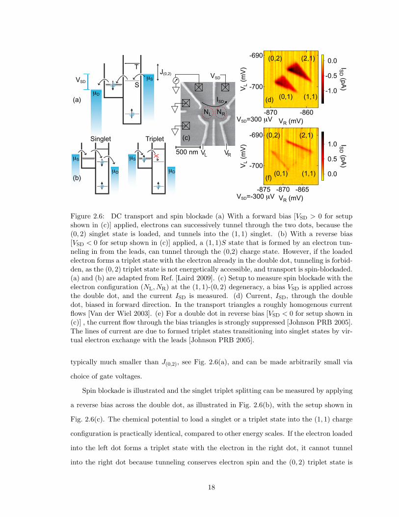
2.6 DC transport and spin blockade . . . . . . . . . . . . . . . . . . . . . . . . . 18
2.7 Energy level diagram of two-electron spin system as function of detuning, 20
2.8 Dephasing and inhomogenous dephasing time T ∗2 . . . . . . . . . . . . . . . 22
2.9 Qubit rotations around Bloch sphere z-axis . . . . . . . . . . . . . . . . . . 24
2.10 State tomography and universal qubit gate-control . . . . . . . . . . . . . . 25
3.1 Device, charge stability diagram, energy levels . . . . . . . . . . . . . . . . . 31
3.2 EDSR spectroscopy, spin resonance signal . . . . . . . . . . . . . . . . . . . 33
3.3 EDSR peak strength versus microwave pulse duration, Spin-flip rate versus
applied microwave power . . . . . . . . . . . . . . . . . . . . . . . . . . . . . 35
3.4 Nuclear polarization, created by EDSR . . . . . . . . . . . . . . . . . . . . . 41
3.5 Addressing of spins via magnetic field gradients induced by micromagnets . 42
3.6 Spin resonance signal driven by higher harmonics . . . . . . . . . . . . . . . 44
x

4.1 Device, charge configuration and experimental pulse-cycle . . . . . . . . . . 48
4.2 Single-shot measurement fidelity and visibility . . . . . . . . . . . . . . . . . 50
4.3 Coherent oscillations in nuclear Overhauser field, continous monitoring of
nuclear field gradient . . . . . . . . . . . . . . . . . . . . . . . . . . . . . . . 53
4.4 Ensemble average, fast probing of electron-nuclear spin interaction . . . . . 55
5.1 Device, sensor conductance as a function of nearby gate . . . . . . . . . . . 60
5.2 Charge stability diagrams measured via SQD and QPC (dc measurement) . 61
5.3 Single-shot measurement SNR for SQD and QPC . . . . . . . . . . . . . . . 65
5.4 Numerical simulation of sensor conductance for SQD and QPC . . . . . . . 67
6.1 Device image, charge stability diagram, pulse sequence . . . . . . . . . . . . 74
6.2 Energy level diagram, triplet relaxation channels, singlet initialization, relax-
ation rate and measurement point exchange energy. . . . . . . . . . . . . . . 76
6.3 Time evolution of nuclear polarization, singlet triplet precession visibility. . 81
6.4 Triplet relaxation time in measurement point, charge relaxation rate, mea-
surement visibility as function of magnetic field gradient. . . . . . . . . . . 83
6.5 Magnetic field gradient dependence of triplet relaxation rate and singlet-
triplet precession visibility for two different applied magnetic fields. . . . . . 86
6.6 Singlet initialization fidelity as function of magnetic field difference. . . . . 89
7.1 Device, charge stability diagram, pulse sequence, energy level diagram and
qubit Bloch sphere. . . . . . . . . . . . . . . . . . . . . . . . . . . . . . . . . 93
7.2 Decoherence protection of singlet-triplet superpositions, interlacing of oper-
ations and spin echo sequences. . . . . . . . . . . . . . . . . . . . . . . . . . 96
xi
7.3 Comparison of spin echo recovery amplitudes for Hahn echo, Carr Purcell,
Concatenated dynamical decoupling (CDD) sequence with 21 π-pulses,and a
22nd order Uhrig Decoherence Decoupling (UDD) . . . . . . . . . . . . . . 98
B.1 Reflectometry, Principle, Setup and Signal . . . . . . . . . . . . . . . . . . . 120
B.2 RF-setup and components . . . . . . . . . . . . . . . . . . . . . . . . . . . . 123
F.1 Scanning Electron Microscope Images of etched trenches in GaAs, width as
Function of Design Width and E-Beam Dosage . . . . . . . . . . . . . . . . 146
xii
Acknowledgements
With the completion of my Ph.D. in sight, I can take the luxury to pause and remember
the people who guided me in and contributed to this work, were part of my daily life and
shared the excitement, fun and pain.
My first thanks naturally goes to Charlie who offered guidance, inspiration, support
and impellent throughout all of my dissertation. Charlie invited me into his group and
paired me with great teachers in the form of David Reilly and Jason Petta. He gave me
challenging and exciting projects to work on, but he also gave me the means to do so. That
means on the one hand excellent equipment, a shipshape lab and sufficient cryogens in order
to stop an experiment not until it is done. On the other hand, and more importantly, he
provided me with excellent mentors, David, Jason, Jake Taylor, Emmanuel Rashba, Mike
Stopa, Hendrik Bluhm, Amir Yacoby, and most importantly himself.
A great physicist who not only has a deep understanding of theory but who also is a
true experimentalist, Charlie guided my thought process while also teaching me how to
wield a blowtorch to repair a broken refrigerator. He lead by example in keeping the lab
orderly by personally putting tools away. He maintained a balance of being an authoritative
figure, encouraging us to work hard, but also being someone we would enjoy grabbing beers
and cracking jokes with. Charlie is a great example of a well-rounded physicist - he talks
about Shakespeare, politics, movies and other worldly things, while still maintaining a deep
understanding of his field. His example made me doubt my decision to leave science multiple
times.
I am very happy to have chosen Charlie as an advisor. He always supported me, even
in my choice not to follow an academic career path. With the choice of an advisor comes
the choice of a lab and thus of lab mates, with whom most of the waking hours of five years
xiii
are spent, or, as in Jimmy’s case, sleeping hours as well.
We few, we happy few, we band of brothers1
this quote, intended to motivate the English footmen to throw themselves against the french
knights against all odds, in some sense describes the cohesion and determination of the
members of the Marcus lab2. Motivated to throw themselves against the odds of getting a
******** experiment or device to work and getting out of graduate school somewhat sane,
all Marcusites are united in the determination to work hard and do things right, lead by
the example of Charlie. I am grateful for having had the chance to share the lab with many
great undergraduate students, graduate students, post-docs and visitors.
David Reilly welcomed me to the group, and taught me about dilution refrigerators,
which I - as a former atomic physicist - knew nothing about at the time. After a short
time with David I went through the hard but thorough school of double dot fabrication and
quadruple-dot tuning of Jason Petta. Jason is a one hundred percent determined physicist,
who taught me nano-fabrication, running a dilution refrigerator and the tricks of device
tuning. His strict training prepared me well for the following years. Alex Johnson always
seemed to know an answer or solution when asked for help or advice, and furthermore an
aura of calm emanated from him. Another dear companion from the early years is Leo
DiCarlo, who not only offered advice, taught me about noise and save me from a nervous
breakdown when I falsely thought I had blown up Jason’s device 3. He is also a very pleasant
person to be around and to work with, and he always was a good sport when teased or
made fun of. After working with Jason I was paired to work with Edward, or ”Oh-Gosh”
as he was lovingly called due to his frequent mutterings during lab-mishaps. The results
presented in chapter 3 were obtained in collaboration with Edward. For a short time, Colin
1Shakespeare, Henry V
2At times, you would omit happy.
3Leo helped me track down the problem to a broken Lock-in.
xiv
Dillard was a Marcusite and worked with us figuring out the etching technique discussed in
appendix F.
Other people visited the lab shortly during that time. Slaven, Tim, Andrew, Rob,
Thomas, who I had the pleasure to meet again in Copenhagen, and Michi, who will be
remembered not only for his attempts at cursing in English, were great people to work
around. I also thank Michi for hosting me during my visit to the Tarucha lab in Tokyo
which I enjoyed very much. Jen Harlow 4 and Carolyn Stwertka were really fun people to
share the lab with, not only because they introduced me to great American literature, like
No girls allowed.
In the later years I had the pleasure to share the lab with Jacob Aptekar, who would
keep us entertained for hours during group meeting, Yiming Zhang and Doug McClure. The
latter two already were in the lab before I joined, but making the move to LISE, and as in
Doug’s case outlasting me, makes them count into the later years. Doug’s tireless efforts to
ensure our data is backed up are appreciated. Jeff Miller and his plants, now slowly dying,
as well as My Linh Pham - all in pink - brightened up the lab. Hugh Churchill always made
his few words count, recently even cracking jokes - unexpected at first.
Many thanks to David and Jimmy, who during the typically dark third year of graduate
school would help me maintain sanity and keep assuring me of the light soon to be at the
end of the tunnel. David’s jolly nature and his endless supply of funny, odd and interesting
stories always took the weight off days of hard work. His great find in McKay, back in the
days, will always be remembered. His contribution to the work presented in chapter 4 was
elemental and I am grateful for what he taught me about electronics and radio-frequency.
Jimmy was a great friend and invaluable partner in duels of wit, not only involving ancestral
mention. He always made a great example, working extremely hard but still taking time
to socialize, help out others and be a fun person to be around. Danielle also deserves
lots of gratitude, being the slightly older sister, caring for the Marcusites, well beyond her
exceptionally well done job as an administrator. Reuter cheered us up whenever possible
4Not actually a short-term visitor, but compared to being a graduate student, undergrad research is overquick and painless.
xv
by hiding easter treats, bringing her adorable kids, and coming out dancing with us.
Maja the bird, formerly known as the bee, always was one of the boys. Chris and
her would be up for dinner and beer, even host christmas parties for the lab orphans. She
would even occasionally donate her Helium when other’s experiments were at stake. Angela,
despite her two-dimensionality, always proved large capacity to deal with crude jokes from
us boys, and brightened up the lab with her high spirit. I am very grateful to Jim Medford,
not only for replacing me and continuing the work on my project, but also for being a
great collaborator. It was a pleasure to train Jim, and to see him grow into a partner, who
contributed much work to the last two chapters of this thesis. Aside from being a hard-
working colleague he is a fun person to work and hang out with as well, often demonstrating
how a link to cannibalism or zombies can be found in any topic of conversation.
Nocturnal Patrick was an amazing study on how a person can exist without food or sleep
but still be a really nice guy. Jonah was a pleasant person to work with, always friendly
and interested in discussion. Teesa not only surprised by learning everything Edward knew
in 3 weeks. She also impressed with very high ethics and responsibility, and by being a
person everybody in lab loved to spend time with. Ferdinand is a phenomenon, he forgets
everything and everyone while doing lab-work or thinking about physics. Despite these
light streaks of autism and his quirks, he is one of the kindest people I met over the years.
His stories are always entertaining and he can be relied on without doubt 5. Sandro was a
source of calm and friendliness. Menyoung would not only amuse by quoting numbers as
N , but he was also be patient in teaching me Korean and come out to drink with us. Max
Lemme, who turned out to be much younger inside than marriage, kids and gray hair led
to expect, was happy to listen and give advice as well as to partake in foolish joking around
with us. Thanks to Willy for advising me on photography. He as well as Anna, and Ruby
will make a good new generation of Marcusites.
Outside of the Marcus lab, Jake Taylor became a partner in stimulating and instructive
conversations early in my Ph.D. and remained one until the very end. I was happy to
5except for proof-reading thesis chapters
xvi
discuss ideas related to the work in chapter 3 with Mark Rudner. Discussing physics but
also especially non-physics with Frank Koppens was always enjoyable. It was a great honor
for me to work with Emmanuel Rashba who, despite his impressive achievements, surprised
by his modesty and kindness. I found it stimulating to collaborate with him on the work
presented in chapter 3, and was able to learn much from him. His passion for physics is
contagious. I enjoyed the stories he shared from his rich experience and I am happy to have
him on my Ph.D. committee. Mike Stopa was not only a great person to work with on the
paper which is presented in chapter 5, he also also a great companion to go out with in
Tokyo. Morten is a quirky physicist, with whom I enjoyed collaborating together with Mike
and Jim on the work in chapter 5. It was fun to go out in Copenhagen as well as in Boston.
Without the 2DEG, grown by Micah Hanson at UCSB, whom unfortunately I never met,
this thesis would not have been possible.
I thank Amir for the pleasure of having him on my Ph.D. committee, and working
with him on the paper presented in chapter 6. Discussion with him was always stimulating
and his questions are always succinct and instructive, and kept me on my toes during my
qualifying exam. Sandra Foletti not only displayed a high level of genuine openness when we
were working on two different yet very similar experiments. She was also a pleasant person
to interact with both in physics discussion and non-physics related conversation. Hendrik
Bluhm became one of my late-stage mentors and it was a pleasure to collaborate with him
on the work presented in chapter 6. He has a deep love for physics and many hours passed
discussing or arguing with and learning from him. Mikey, Gilad and Vivek were a fun bunch
who always happily shared the riches of the food in the Yacoby lab kitchen.
None of the work in this thesis could have been completed without the hardworking
people at CNS and DEAS, many thanks to Steve Shephard, Noah Clay, Steve Sheppard,
Ed Macomber, Jiangdong Deng, Ling Xie and Yuan Lu at CNS, and to Louis Defeo and
his colleagues in the machine shop, as well as to James McArthur. I am grateful to the
administrators of the Marcus lab during my time here, James Gotfredson, and Jess Martin
and Rita Filipowicz, who always made sure Helium or other necessities were ordered and
my stipend was paid.
I also want to thank my mentors and advisors before I started my Ph.D.. Professor Jodl
xvii
enabled me to engage in research before entering University and in my early undergraduate
semesters. Jorg Kreutz was a great teacher during these early years. Isaac Silvera enabled
me to do exciting research during a semester abroad at Harvard, made me feel welcome in
the US. It was always stimulating to discuss physics with him. Sandeep Rekhi, Eran Sterer,
Gerhard Bohler, Ako Chijioke were great coaches and companions during my short visit in
Ike’s lab.
For my Master’s thesis I had the luck to work with Klaas Bergmann who is not only
a great experimentalist and physicist but also a gifted manager and a great mentor who
cares a great deal about the advancement of his students and mentees. I am also grateful to
Frank, Manfred, Anett, Zsolt, Aigas, Vladimir, and Ruth whose company and partnership
during my Master’s thesis was very valuable to me.
Last but not least, I want to thank all of my friends, loved ones and my family who
supported me on the way to and during my dissertation. I am especially indebted to my
parents and grandparents without whom I would not be where I am now, as they gave me
a strong foundation to build on. I could always count on their support and love.
xviii
Chapter 1
Introduction
1.1 Organization of this Thesis
In chapter 1, after this brief outline, I give a broad overview of the motivation for the work
presented in this thesis, followed by a summary of what I believe are the key contributions.
Chapter 2 starts with a brief introduction to spin qubits, which are central to this thesis,
before giving a brief overview of the physics of gate-defined double quantum dots in GaAs
heterostructures and some of the experimental techniques used in this thesis. Finally, a
necessarily incomplete list of important, previous contributions to the field of GaAs spin
qubits, that put the work in the following chapters in context, is discussed.
In chapter 3, experiments on single-spin qubits are presented. A mechanism of electric
dipole spin resonance, driven by an electric field and mediated by hyperfine coupling is
described. While the coherence of the evolution is lost due to the randomly fluctuating
hyperfine fields, this method of spin manipulation is technically simpler than conventional
magnetically driven spin resonance, because time-varying electrical fields can be created
more easily on the nanoscale. The effect is useful for spectroscopic measurement of the
magnetic fields at the quantum dots, for average and difference fields, and for the creation
of nuclear polarizations.
In chapters 4 - 7, experiments on two-electron spin qubits are presented. Chapters 4 and
5 describe methods to rapidly determine the two-electron spin state in a single quantum
measurement. In chapter 6 the influence of magnetic field gradient on triplet relaxation
time is investigated, in chapter 7 the coherence of the singlet-triplet qubit is studied.
1
Chapter 4 discusses an experiment demonstrating the single-shot measurement of a
singlet-triplet spin qubit. While previous measurements of the state of a two-electron qubit
constituted ensemble averages over many individual measurements, in this work, a single
quantum mechanical measurement identifies the qubit state as singlet or triplet. The mea-
surement fidelity and visibility of the single-shot measurement are analyzed. The readout
is used to monitor the time-evolution of the Overhauser field difference between two quan-
tum dots, and to investigate the different time scale of the evolution of transversal and
longitudinal nuclear spin components.
In chapter 5, the use of a sensor quantum dot (SQD) as a charge detector is demon-
strated, and shown to provide a significant improvement over the work presented in chapter
4. Results from numerical simulations that are in qualitative agreement with the experiment
are discussed. The numerics show that the improved sensitivity of the sensor quantum dot
results from reduced lifetime broadening and reduced screening.
In chapter 6, I discuss experiments that were aimed to understand phenomenology
presented in Ref. [Reilly 2008] and initially attributed to the preparation of a special nuclear
spin state with zero polarization gradient. The experiments elucidate the mechanism of
triplet relaxation during the two-electron spin measurement, the influence of magnetic field
gradients on spin relaxation rate and on initialization and readout of the singlet-triplet
qubit.
Chapter 7, describes experiments aimed at studying and extending qubit coherence.
The interlacing of qubit rotations about two different Bloch sphere axis with Carr Purcell
spin echo pulses is demonstrated as an initial step to coherence-protected qubit operations
and to show that spin echo sequences extend the coherence of singlet-triplet superpositions
as well as the coherence of initial singlet states. The coherence times of an initial singlet
state for different types of spin echo sequences are compared.
Appendices give further physical background, and technical information related to the
experiments. Appendix A details the fabrication recipe used to create the devices discussed
in chapters 3-7, and comments on the difficulties fabricating nanoscale devices with micro-
magnets. In appendix B, I give a short introduction to rf-reflectometry which was essential
to obtain the results of chapters 4 and 5. Appendix C presents calculations estimating signal
2
and noise of rf-measurements in chapters 3 and 4.Appendix D gives supplementary material
to chapter 4 and Ref. [Barthel 2009], presenting the derivation of an equation. In Appendix
E inhomogeneous dephasing in spin-echo experiments due to electrical pulse imperfections
and drifts, is estimated. Appendix F briefly discusses the viability of etching techniques to
be combined with depletion gates in GaAs quantum dot fabrication.
1.2 Motivation
1.2.1 Quantum Control over single Spins interacting with a Bath
Anyone who is not shocked by quantum theory has not understood it.
Niels Bohr
Quantum mechanics, while widely applicable and believed to be the most accurate
description of nature, still offers mysteries and puzzles that are not completely under-
stood. Among the most prominent open questions or ”mysteries” are entanglement, the
process of measurement, the fractional quantum hall effect and the phenomenon of deco-
herence. In quantum mechanics, a particle or system can be in a superposition of two
distinct states, for example being located simultaneously at two different positions, or - in
the case of an electron spin - pointing up and down at the same time. This is not sim-
ply a mathematical oddness, but the superposition principle is experimentally confirmed.
In the ’classical’ world that we observe everyday, there are no superpositions, as illus-
trated by the famous Schroedinger’s cat paradox [Schrodinger 1935]. Generally, the laws
of quantum mechanics hold at small length scales, small temperatures and only over short
times, while for macroscopical objects a classical, non-quantum mechanical description is
completely adequate. Interaction of quantum mechanical systems with their environment
leads to decoherence and, hence, classical behavior. In the framework of quantum me-
chanic a measurement ”collapses” the state of the system into the state corresponding to
the measured observable [Wheeler 1983]. Weak measurements, however, can infer infor-
mation about a quantum state without collapse while yielding non-intuitive measurement
results [Aharonov 1988; Romito 2008; Katz 2008].
3
Electron spins in solids are ideal systems to study fundamental quantum mechanics and
decoherence. Recent advances in nanoscale fabrication techniques gave birth to mesoscopic
physics, allowing for length scales smaller than the particle’s coherence length, such that
quantum effects become important, but still large enough for the particle to interact with
many other particles.
Multiple electron spins can create long-lived superposition and entangled states, and
full experimental control over the Hamiltonian can be achieved electrically. The spin states
are coupled to the host material via hyperfine and spin-orbit interaction. These interactions
result in finite lifetime of superpositions and of entangled electron spin states, via the entan-
glement of the electron state with the environment. The evolution of electron spins, their
interaction with each other and with the environment can therefore be electrically tuned to
a wide degree. The spin state can be measured on individual spins, and in the experiments
discussed in chapters 4 and 5 the spin state of a two-electron system is determined in a
single quantum mechanical measurements.
1.2.2 Quantum Computation
Motivated by the simulation of physical systems Richard Feynman suggested the use of
a quantum computer, with the information encoded in the quantum state of the system
and the operations performed via unitary operations [38; Mermin 2007]. The probabilistic
nature of physics, and multiple particle interaction and entanglement make the simulation
of many physical problems too complex to solve in a classical computer, while a quantum
computer possesses the same large number of degrees of freedom as a physical system of
study. In a quantum computer, the bits that contain the information 1 or 0 are replaced by
qubits (quantum bits) that can be in any quantum mechanical superposition of 0 and 1. As
a whole, a quantum computer can be in a superposition, in multiple (or all possible) states
at the same time, and therefore perform multiple (or all possible) operations simultaneously.
Due to this quantum parallelism, a quantum computer is significantly more efficient
than a classical computer in the solution of certain computational problems, as was realized
a full ten years after Feynman’s initial proposal by Bruce Shore [Shor 1994] . The quantum
algorithms most widely known are Shor’s algorithm and Grover’s algorithm. Shor’s algo-
4
rithm allows to factorize numbers in an amount of time that scales as N2, for a number with
N digits, while the scaling with N for a classical algorithm is eN1/3 [Shor 1994]. Unique
solutions to mathematical functions with arguments of N bits can be found in a time that
scales as 2N/2 using Grover’s algorithm, while the classical scaling is as 2N [Grover 1997].
The biggest challenge in quantum computation is decoherence, which tends to make all
systems behave classically at high temperatures, for large numbers of interacting particles
and after long times over which a system evolves. Coupling to an environment always leads
to decoherence, and cannot be avoided as the quantum computer needs to be controlled,
and read out.
Recent results, however, give hope (and continued funding) to the quantum computa-
tion community. It was found by DiVincenzo that any unitary transformation on a collec-
tion of qubits can be decomposed into a series of one- and two-qubit unitary transforma-
tions [DiVincenzo 1995; Barnenco 1995]. Furthermore, it has been shown that an approxi-
mation of arbitrary single qubit operations by a discrete subset of transformations on a single
qubit is sufficient for the realization of quantum computation [Kitaev 1997; Mermin 2007].
Quantum error correction allows to perform quantum computation in the presence of im-
perfect gate operations [Steane 1996].
Electron spins in semiconductor quantum dots are a promising system to form the qubit
for quantum computation [DiVincenzo 1998; Loss 1998]. Electron spin qubits are compar-
atively insensitive to decoherence and dissipative initialization in a ground state is possible.
Such a system can in principle be integrated with conventional semiconductor electronics,
and the tools available to the semiconductor industry can be used in the fabrication and
measurement of devices.
1.2.3 Spintronics
Electronics was one of the success stories of the 20th century. For 50 years, the exponential
growth in computational power and functionality has followed Moores law, which predicts
a doubling of the number of transistors per chip every 18 months. Conventional electronics
relies on the encoding of information into electrical voltages and currents, and information
storage typically is handled differently from information processing. Heat dissipation is a
5
burning issue especially as devices shrink and insulating layers get thinner thereby increasing
leakage currents. The reduction in device size faces an unsurmountable boundary as atomic
length scales are approached.
Employing the electron spin as the smallest unit of information, even without harnessing
the powers of quantum computation, promises several advantages over conventional elec-
tronics [Prinz 1998; Das Sarma 2001; Datta 1990]. In spin electronics (spintronics), storage
and manipulation can in principle be done in the same devices, and a reduction of power
dissipation and device size is possible.
In order to realize spintronic devices, we need to understand how spins are transported
through materials, how to create aligned spins, and how to manipulate and control the
direction of spins. Semiconductor quantum dots offer highly tunable systems in which spin
dependent electron transport and electron tunneling can be studied. Experiments investi-
gating decoherence of electron spins may provide insights that help to preserve information
in spintronics devices. Decoherence and spin relaxation are important parameters. Methods
to electrically manipulate spin may prove useful as tools in applications or in basic research
on electron-spin devices.
1.3 Summary of Contributions
The key contributions reported here are as follows:
• In Chapter 3, electrically driven spin resonance of a single electron is demonstrated.
By studying the magnetic field dependence of the resonance strength, it is shown that
a novel mechanism couples the electric field to the electron spin, namely a fluctuating
hyperfine field. Driving the resonance is found to create a nuclear polarization in the
quantum dot. Using a micromagnet to create a magnetic field gradient across the
device, a technique to address individual spins in a multi-electron device is presented.
• In Chapter 4, rapidly repeated high-fidelity (> 90%) single-shot measurements of a
singlet-triplet qubit is demonstrated for measurement times of a few microseconds.
Quasi-static nuclear Overhauser fields are observed and their evolution is monitored.
A model of single-shot readout statistics that accounts for T1 relaxation, is developed.
6
It is shown that the transverse component of the Overhauser field difference is not
quasi-static on the time scale of data acquisition, as expected theoretically.
• In Chapter 5, the use of a sensor quantum dot (SQD) for fast charge and two-electron
spin-state measurement are demonstrated. The performance of the SQD is compared
to quantum point contact (QPC) sensors for dc and radio-frequency (rf) measurement.
The SQD is up to 30 times more sensitive, provides roughly three times the signal
to noise ratio (SNR) of a comparable QPC. Numerical simulations, also presented,
elucidate the role of screening in determining the sensitivity of proximal charge sensors.
• In Chapter 6, nuclear polarization gradients built by electrical pump-cycles are in-
vestigated. An increased triplet relaxation rate, during measurement, with increasing
nuclear field gradient is found and characterized. A model describing triplet decay is
developed, describes the data well and provides guidance in the choice of parameters
to improve measurement visibility. Initialization and readout fidelity of the qubit in
the presence of field gradients are studied as function of pulse rise- and ramp- times.
• In Chapter 7, the protection of a singlet-triplet superposition from decoherence is
demonstrated by interlacing qubit rotations about two different Bloch sphere axes
with Carr Purcell spin echo pulse sequences. Coherence times of a singlet, decou-
pled by a single Hahn echo, a Carr Purcell echo sequence with 16 π-pulses, a 5th
order Concatenated dynamical decoupling sequence, and a 22nd order Uhrig decoher-
ence decoupling sequence are compared. Singlet coherence times beyond 100 µs are
achieved.
7
Chapter 2
Spin Qubits in GaAs DoubleQuantum Dots
2.1 Spin Qubits
A qubit for quantum information processing can be realized by any two-level system, which
allows for manipulation of its state, that can be coupled to another two-level system, and
that can be measured. The challenge lies in the coupling qubits to each other and to a
classical control apparatus, to enable manipulation of the qubit state, without inducing
decoherence.
Electron spins are arguably the most fundamental manifestation of a quantum mechanical
two-level system. They are promising candidates for qubits, because the spin does usually
not strongly couple to the environment, while the charge of the electron allows to localize,
move and manipulate the system electrically. The two implementations, on which most
work has been done in recent years, are single-spin and two-electron spin qubits. Both are
discussed briefly in the following.
2.1.1 Single-Spin Qubits
In single-spin qubits [Loss 1998], the information is encoded in the quantum state of a
spin in a large applied magnetic field (> 1 Tesla) [Elzerman 2004]. The basis states of the
qubit are the states |↑ and |↓, the spin being parallel or anti-parallel to the applied field
respectively. The qubit bloch sphere, a graphical representation of the state of the two
level system, is shown in Figure 2.1.1(a). Large applied fields are needed to create a large
8
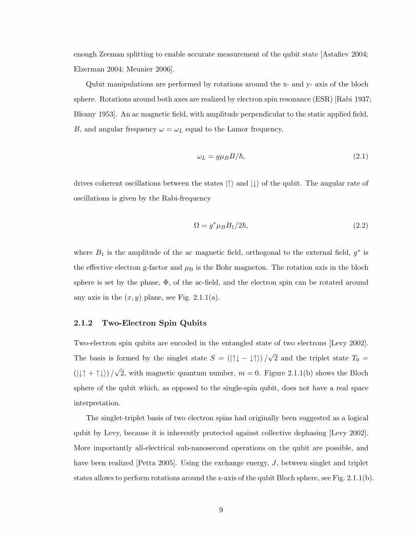
enough Zeeman splitting to enable accurate measurement of the qubit state [Astafiev 2004;
Elzerman 2004; Meunier 2006].
Qubit manipulations are performed by rotations around the x- and y- axis of the bloch
sphere. Rotations around both axes are realized by electron spin resonance (ESR) [Rabi 1937;
Bleany 1953]. An ac magnetic field, with amplitude perpendicular to the static applied field,
B, and angular frequency ω = ωL equal to the Lamor frequency,
ωL = gµBB/, (2.1)
drives coherent oscillations between the states |↑ and |↓ of the qubit. The angular rate of
oscillations is given by the Rabi-frequency
Ω = g∗µBB1/2, (2.2)
where B1 is the amplitude of the ac magnetic field, orthogonal to the external field, g∗ is
the effective electron g-factor and µB is the Bohr magneton. The rotation axis in the bloch
sphere is set by the phase, Φ, of the ac-field, and the electron spin can be rotated around
any axis in the (x, y) plane, see Fig. 2.1.1(a).
2.1.2 Two-Electron Spin Qubits
Two-electron spin qubits are encoded in the entangled state of two electrons [Levy 2002].
The basis is formed by the singlet state S = (|↑↓ − ↓↑) /√
2 and the triplet state T0 =
(|↓↑ + ↑↓) /√
2, with magnetic quantum number, m = 0. Figure 2.1.1(b) shows the Bloch
sphere of the qubit which, as opposed to the single-spin qubit, does not have a real space
interpretation.
The singlet-triplet basis of two electron spins had originally been suggested as a logical
qubit by Levy, because it is inherently protected against collective dephasing [Levy 2002].
More importantly all-electrical sub-nanosecond operations on the qubit are possible, and
have been realized [Petta 2005]. Using the exchange energy, J , between singlet and triplet
states allows to perform rotations around the z-axis of the qubit Bloch sphere, see Fig. 2.1.1(b).
9
J Bz
(a) (b)
xz
yx
z
ycos( B1
sin( B1
Figure 2.1: Single-spin and two-electron spin qubit bloch spheres (a) The Bloch sphere isa graphical representation of the quantum state of a two-level system, in our case of thedirection an electron spin. The inclination from the z-axis θ is determined by the probabilityamplitude of the spin superposition state, P↑ = cos2 θ, while the azimuthal angle givesthe phase of a superposition state of two spin directions. Rotations about the x- and y-axis of the Bloch sphere are realized via an oscillating magnetic field with amplitude B1,perpendicular to the applied static magnetic field, see text. The phase of the oscillating fieldΦ sets the axis of rotation on the Bloch sphere. (b) The Bloch sphere of the two-electronspin qubit does not have a real space interpretation, as opposed to the single-spin qubit.The qubit is spanned by the singlet and triplet states S and T0 and rotations around the z-axis of the Bloch sphere are induced by an energy difference, J , between singlet and triplet,see section 2.5. Rotations around the x-axis are driven by the projection of a magnetic fielddifference between the two electrons,∆ Bz, onto the average magnetic field direction.
Qubit rotations around a second independent axis are needed for universal control, and can
be induced around the x-axis of the Bloch sphere by a magnetic field difference,∆ Bz,
between the two electrons. A field difference for these rotations can be realized via a
micro magnet, [Pioro-Ladriere 2007] and has recently been realized via a gradient in the
nuclear polarization of the host material containing the electron spins, see section 2.5 and
Ref. [Foletti 2009].
Single-shot readout of the qubit has been realized as part of the work presented in
this thesis and is discussed in Ref. [Barthel 2009] and chapter 4. Coherence times over
200 µs can be achieved using a spin echo sequences [Hahn 1950; Carr 1954; Meiboom 1958;
Bluhm T2 2010] to suppress hyperfine dephasing [Petta 2005]. Thus all necessary compo-
nents for single qubit operations have been implemented, however not simultaneously in
a single experiment. Two-qubit operations have not yet been realized, however promising
progress has been made towards the coupling of two adjacent double quantum dots [Laird 2010],
each of which would contain a two-electron spin qubit [Taylor 2006].
10
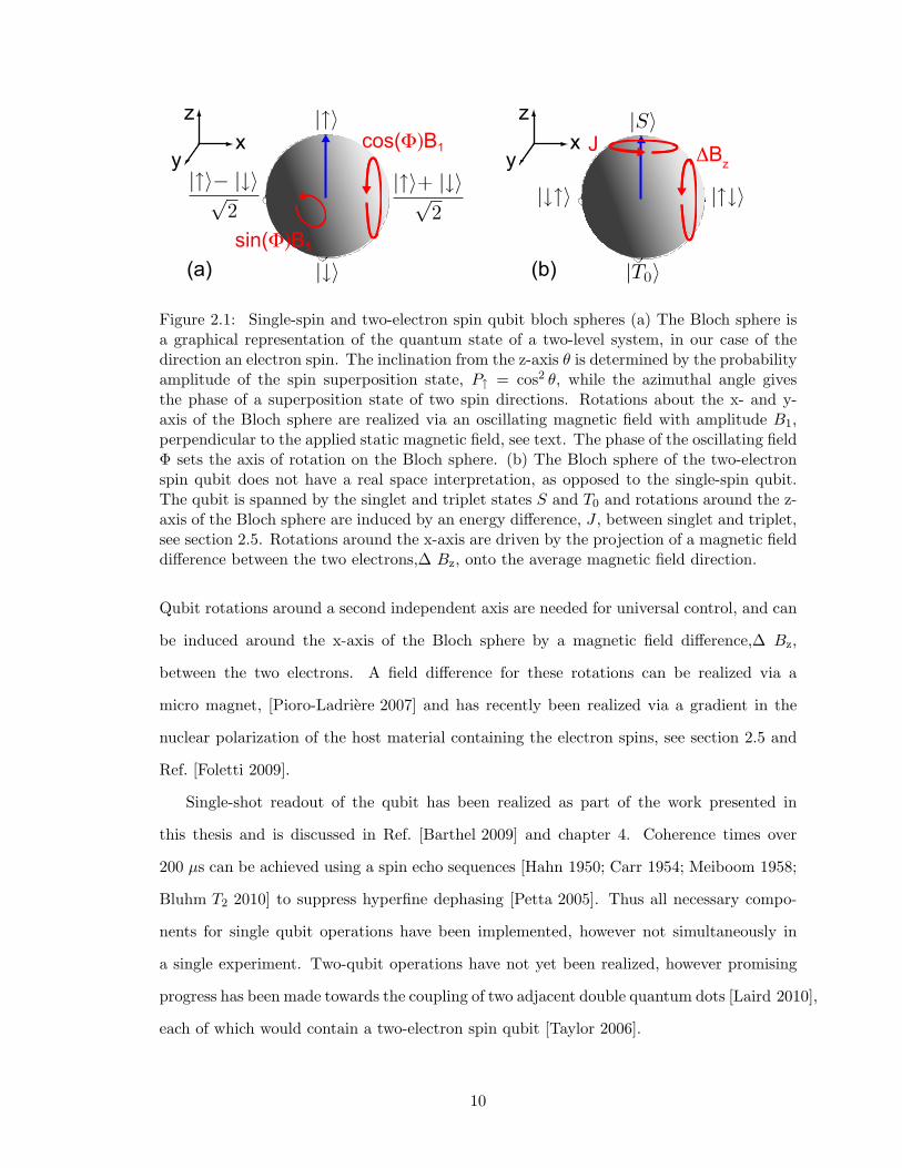
2.2 GaAs Heterostructures and Depletion Gates
GaAs heterostructures are ideal systems to study confined electrons and electron spins.
They provide confinement for electrons in one direction by an electronic band structure
tailored to the experimental needs. At low temperatures the confined electrons behave
like a two-dimensional electron gas (2DEG), as they are free to move in the directions
perpendicular to the confinement direction [Beenakker Review 1991; Johnson Thesis 2005].
Very clean crystals are grown by molecular beam epitaxy (MBE) [Drummond 1986] on top
of a GaAs substrate, as illustrated in Fig. 2.2(a). A superlattice, 30 alternating layers of
GaAs and Al0.3Ga0.7As, is deposited on the GaAs substrate by MBE, in order to minimize
lattice mismatch at the heterostructure. The experimental system is created by a layer
of Si dopant atoms, that forms and donates electrons to a triangular quantum well at the
interface of the 800 nm GaAs- and the 100 nm Al0.3Ga0.7As layers. One of the bound
states of the triangle well, indicated by the thick solid line in the energy level diagram in
Fig. 2.2(a), lies below the Fermi energy and forms the 2DEG, while other sub-bands [thick
dashed line in Fig. 2.2(a)] are not occupied at low temperatures.
The electrons in the 2DEG can be further confined by application of negative voltages to top
gates, as illustrated in Fig. 2.2(b). Metallic gates, patterned by electron-beam lithography
and deposited by thermal or electron-beam evaporation, create Schottky diodes. These
diodes are reverse-biased by negative voltages, which locally change the electric potential
experienced by electrons in the 2DEG underneath. For voltages low enough, the region of
2DEG directly underneath the gate can be depleted, completely emptied of electrons, as
indicated by the dashed line region of the 2DEG underneath the gates in Fig. 2.2(b). In
this work the top gates are realized by a 15 nm layer of gold on top of a 5 nm layer of
titanium to ensure strong adhesion of the gold to the GaAs wafer, see Appendix A.
The 2DEG is electrically contacted by a mixture of Gold and Germanium that diffuses
down to the 2DEG from Platinum-Gold-Germanium contact pads during a thermal anneal-
ing step, see Fig. 2.2(b). The contact pads are deposited on the surface of the wafer by
photo-lithography and electron-beam evaporation. Details are provided in Appendix A.
The schematic in Fig. 2.2(a) shows the parameters of the wafer 050329A grown by Micah
11
500 nm
VAC
VG
10 nm - GaAs cap
60 nm - Al0.3Ga0.7As
4 x 1012 cm-2 - Si -doping
40 nm - Al0.3Ga0.7As
800 nm - GaAs
30-period superlattice3 nm Al0.3Ga0.7As, 3 nm GaAs
500 m - GaAs substrateenergy
2DEG
fermi level
Figure 2.1: Wafer structure of a 2DEG. At right the energy of the conduction bandedge is shown schematically vs. depth. A trianglular potential well is formed at theburied GaAs/AlGaAs interface with one subband (thick solid line) below the Fermilevel. Other subbands (thick dashed line) are inaccessible. The specific parametersshown here describe the nominally identical wafers 010219B and 031104B, grown byMicah Hanson at UCSB, which were used to make all of the devices used in theexperiments in this thesis.
measuring this endless variety of devices.
2.1 GaAs/AlGaAs heterostructures
The first step in creating a GaAs nanostructure is to make a two-dimensional electron
gas (2DEG) [26] at the interface between GaAs and AlxGa1−xAs (typically x ∼ 0.3)
as shown in Fig. 2.1. Positively charged donors (usually group IV silicon atoms
substituting for group III gallium or aluminum) are placed tens of nanometers away
from the interface in the AlGaAs region. Because AlGaAs has a larger band gap
than GaAs, the global potential minimum is not at the donors but at the interface
7
(a) (b)2 DEG
Ohmic
contacts
Figure 2.2: GaAs heterostructure and depletion gates. (a) Schematic of GaAs/AlGaAs het-erostructure (left), shows layers of GaAs, and Al0.3Ga0.7As that are deposited to form a tri-angular potential well at the interface of the 800 nm GaAs layer and the 100nm Al0.3Ga0.7Aslayer, as shown by the profile of the conduction band on the right. One sub-band (thicksolid line) lies below the Fermi level and forms the two-dimensional electron gas (2DEG),while other sub-bands (thick dashed line) are not occupied at low temperatures. The spe-cific layer-thicknesses are for the wafer 050329A (grown by M. Hanson in the group of A.C.Gossard at U.C. Santa Barbara), which is used in the experiments described in this the-sis. (Image adapted from Ref. [Johnson Thesis 2005]) (b) Ohmic contact is made to the2DEG by thermal annealing of Pt/Ge/Au pads (black spikes, see Appendix A), allowingmeasurement of charge transport through devices. Negative gate voltages, VG, are appliedto metal top gates (light gray), to deplete the (2DEG) underneath and form constrictions,like quantum point contacts (QPCs) or quantum dots.
Hanson in the Gossard group at U. C. Santa Barbara. All experiments described in this
thesis are performed on four devices fabricated from this wafer.
Charge noise and telegraph noise 1 due to switching of charges between donors in the dopant
layer and due to electrons tunneling through the Schottky barriers of top gates [Buizert 2008],
pose a major complications in device tuning and operation. Different wafers have differ-
ent quality, characterized by the absence of switching noise. Limiting the magnitude of
the negative applied gate voltages, aided by the application of a positive bias during cool-
down (see Appendix B.4 of Ref. [Laird 2010] and Ref. [Buizert 2008]), reduces charge noise
as demonstrated in Ref. [Buizert 2008]. If charge noise from the GaAs heterostructure be-
comes the limiting noise, after eliminating noise from dc-wiring and pulse-generators, an
1called switching noise in lab jargon
12
insulator layer between gates and GaAs cap may reduce noise further [Buizert 2008].
2.3 Quantum Point Contacts and Quantum Dots
18 CHAPTER 2
4
3
2
1
0
g (2
e2 /h)
-500 -450 -400 -350 -300Vg (mV)
B = 0 TT = 80 mK
Figure 2-7. Quantized conductance in a quantum point contact. The linear differential conductance, g,through a QPC as a function of gate voltage shows steps, quantized in units of 2e2/h at B = 0, correspondingto the full transmission of spin-degenerate modes through the constriction. This data from QPC 4, describedin Chapter 6.
Vsd
Figure 2-8. Cartoon QPC showing quantized modes. The top drawing shows the two gates of the QPCwith applied gate voltage Vg. Current is restricted to flow through the constriction. The lower drawingindicates the lowest two transport modes, occurring when the width of the constriction is approximatelyone half and one full Fermi wavelength wide, respectively. (Figure courtesy of A. Huibers).
BASIC TRANSPORT IN QUANTUM POINT CONTACTS AND QUANTUM DOTS 19
ky
En
µsµd
EF
Figure 2-9. Energy dispersions for 1D channel. Energy En (for n = 1,2,3) vs. longitudinal wavevector kyfrom Eq. 2.3 at the bottleneck of a QPC assuming parabolic confinement in the lateral direction. Electronsin the source and drain fill the available states up to the chemical potentials µs and µd, respectively. When afinite source-drain voltage is applied, a net current results from the uncompensated occupied electron statesin the interval between µs and µd.
narrowest point of the QPC, which determines the transport properties. We take a parabolic confining
potential in the lateral direction, V(x) = 1/2 m*0
2x2, in accord with Refs. [68, 69]. Solutions to the
Schrodinger equation using this Hamiltonian can be written in the form of a harmonic oscillator with
energy eigenvalues
E nkmn
y( ) *12 0
2 2
2, (n = 1, 2, …). (2.3)
These energies describe 1-D subbands because electrons are free to move in the y-direction (described by
the free-electron kinetic energy dispersion) but quantized in the x-direction. Figure 2-9 shows these 1-D
subband dispersions versus the longitudinal wave vector ky. Electrons in the source and drain leads fill up
states in the Fermi sea to the respective chemical potentials, µs and µd . Considering the orientation of the
QPC shown in Fig. 2-8, electrons moving to the right come from the source and those moving to the left
come from the drain. The velocity of the electrons in each subband is given by vn = (dEn/dky)/ .
When a voltage Vsd is applied between the source and drain reservoirs, the chemical potentials on
each side of the QPC are related as eVsd = µs – µd. The resulting current, I, through the QPC is carried by
the uncompensated states in this energy interval. At zero temperature, the net current is
I e dE E v E T En n nn
N
d
s 12
1
( ) ( ) ( ), (2.4)
(a) (b)
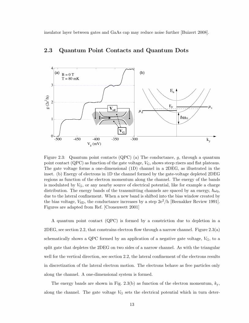
Figure 2.3: Quantum point contacts (QPC) (a) The conductance, g, through a quantumpoint contact (QPC) as function of the gate voltage, VG, shows steep risers and flat plateaus.The gate voltage forms a one-dimensional (1D) channel in a 2DEG, as illustrated in theinset. (b) Energy of electrons in 1D the channel formed by the gate-voltage depleted 2DEGregions as function of the electron momentum along the channel. The energy of the bandsis modulated by VG, or any nearby source of electrical potential, like for example a chargedistribution. The energy bands of the transmitting channels are spaced by an energy, ω0,due to the lateral confinement. When a new band is shifted into the bias window created bythe bias voltage, VSD, the conductance increases by a step 2e2/h [Beenakker Review 1991].Figures are adapted from Ref. [Cronenwett 2001]
A quantum point contact (QPC) is formed by a constriction due to depletion in a
2DEG, see section 2.2, that constrains electron flow through a narrow channel. Figure 2.3(a)
schematically shows a QPC formed by an application of a negative gate voltage, VG, to a
split gate that depletes the 2DEG on two sides of a narrow channel. As with the triangular
well for the vertical direction, see section 2.2, the lateral confinement of the electrons results
in discretization of the lateral electron motion. The electrons behave as free particles only
along the channel. A one-dimensional system is formed.
The energy bands are shown in Fig. 2.3(b) as function of the electron momentum, ky,
along the channel. The gate voltage VG sets the electrical potential which in turn deter-
13
mines the chemical energies of the electron bands. By changing VG, the number of bands
that fall into the bias window can be modified. Each band increases the conductance
by 2 e2/h [Beenakker Review 1991; Cronenwett 2001]. By fixing VG to the threshold, at
which an additional band enters the bias window (one of the steep risers in conductance in
Fig. 2.3(a)), the conductance through the QPC becomes sensitive to the charge arrange-
ment of nearby structures. This enables charge sensing, the measurement of the charge
occupation of quantum dots and other systems, as demonstrated for double quantum dots
in Ref. [Dicarlo 2004] and discussed in more detail in Ref. [Dicarlo Thesis 2007].
200 nmVG
VSDI Rs
QD
Vg
Cg
VdVs
CdCs
Rd
A
Vg
G
NgN
a) b)
Ec
kT eVsd
c) d) e)
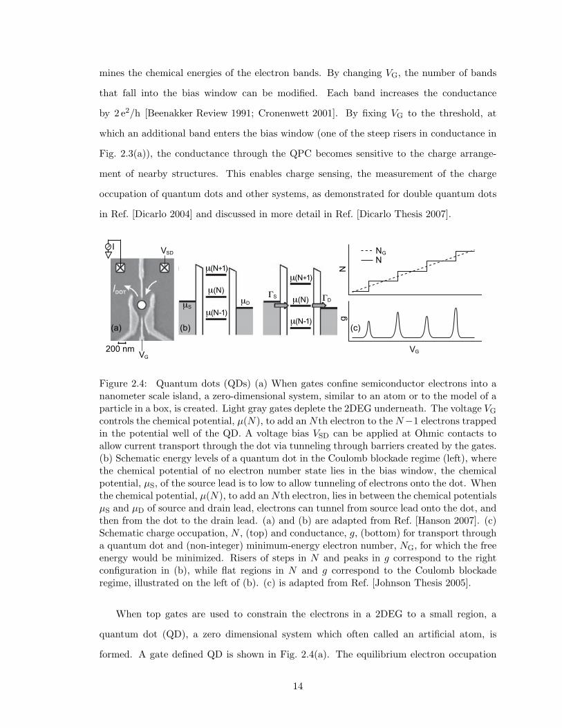
Figure 3.2: Schematic description of a quantum dot. a) Circuit equivalent of a quan-tum dot, showing voltages and capacitances of the source, drain, and gate, tunneling“resistances” to the source and drain, and the current measurement for calculatingconductance. b) The smooth gate charge Ng, resulting dot charge N , and conductancespikes characteristic of Coulomb Blockade. c) Five energy scales determine behaviorof a closed quantum dot. A gap Ec opens up between the occupied n-electron states(solid lines) and unoccupied n + 1-electron states (dotted lines), which are spaced by∆ and tunnel-broadened by Γ, while the leads are characterized by temperature kTand bias eVsd. A transport resonance condition in the quantum regime d) at zerobias, where current flows through only the ground state, and e) at Vsd > ∆, throughground and excited states. The thick solid line represents the newly occupied statein the n + 1-electron ground state. The thin solid and dotted lines represent statesfilled or empty, respectively, in the ground states of both occupancies.
shown on a generic level diagram in Fig. 3.2(c). Two involve the structure of the dot
(Ec and ∆), two concern the leads (kT and eVsd), and one describes the coupling
between them (Γ).8 The first question is what determines whether the dot is open or
8To determine the conductance through the dot it is necessary to know the tunnelrate to each lead, but for delineating regimes of different behavior only their sum isrelevant.
24
VGg
N
NGN
SD
SD
(N)
(N+1)
(N-1)
(N)
(N+1)
(N-1)(a) (b) (c)
Figure 2.4: Quantum dots (QDs) (a) When gates confine semiconductor electrons into ananometer scale island, a zero-dimensional system, similar to an atom or to the model of aparticle in a box, is created. Light gray gates deplete the 2DEG underneath. The voltage VG
controls the chemical potential, µ(N), to add an Nth electron to the N−1 electrons trappedin the potential well of the QD. A voltage bias VSD can be applied at Ohmic contacts toallow current transport through the dot via tunneling through barriers created by the gates.(b) Schematic energy levels of a quantum dot in the Coulomb blockade regime (left), wherethe chemical potential of no electron number state lies in the bias window, the chemicalpotential, µS, of the source lead is to low to allow tunneling of electrons onto the dot. Whenthe chemical potential, µ(N), to add an Nth electron, lies in between the chemical potentialsµS and µD of source and drain lead, electrons can tunnel from source lead onto the dot, andthen from the dot to the drain lead. (a) and (b) are adapted from Ref. [Hanson 2007]. (c)Schematic charge occupation, N , (top) and conductance, g, (bottom) for transport througha quantum dot and (non-integer) minimum-energy electron number, NG, for which the freeenergy would be minimized. Risers of steps in N and peaks in g correspond to the rightconfiguration in (b), while flat regions in N and g correspond to the Coulomb blockaderegime, illustrated on the left of (b). (c) is adapted from Ref. [Johnson Thesis 2005].
When top gates are used to constrain the electrons in a 2DEG to a small region, a
quantum dot (QD), a zero dimensional system which often called an artificial atom, is
formed. A gate defined QD is shown in Fig. 2.4(a). The equilibrium electron occupation
14
of the quantum dot can be changed via a top gate, that changes the size of the dot, or
equivalently the electrostatic energy of conduction band electron trapped in the quantum
dot. Gate voltages also set the potential barrier between the dot and the rest of the 2DEG,
and therefore tune the tunnel coupling between bound states of electrons in the dot and
free electron states in the 2DEG. The quasi-continuum of electronic states of the 2 DEG is
referred to as leads, as they act like metallic contacts to the quantum dot. If the potential
barrier between QD and the leads is large enough, with barrier-conductance e2/h, the
number of charges is quantized, see Ref. [Beenakker Review 1991] for a derivation. Even
though the number of charges, NG, that would minimize the free energy of the system
may be non-integer (dashed line in Fig. 2.4(c), top) the actual number of charges, N , is
an integer [Beenakker CB 1991; Beenakker Review 1991]. When a bias is applied across
a QD, then an electrical current only flows if the chemical potential µ(N) to add an N th
electron to the dot lies in between the chemical potentials of the leads, µS > µ(N) > µD.
Then electrons can hop form the source into the quantum dot and leave it by tunneling
to the drain. If µ(N) lies outside of the bias window, the transport through the QD is
blocked, which is called Coulomb blockade. The conductance of a QD with VG biased on
the steep riser of a Coulom peak (Fig. 2.4(c), bottom) is sensitive to the arrangement of
nearby charges.
The charge occupation of a quantum dot or a double quantum dot (see section 2.4)
can be measured with an adjacent charge sensor, which can be a QPC [Field 1993] or
another quantum dot, as demonstrated as part of this thesis, and discussed in chapter 5. A
change in the charge configuration of the object of interest will act as a change in electrical
potential at the sensor, effectively changing VG and therefore the sensor conductance as
seen in Fig. 2.3(a) and in the bottom part of Fig. 2.4(c).
2.4 Double Quantum Dots and Spin Blockade
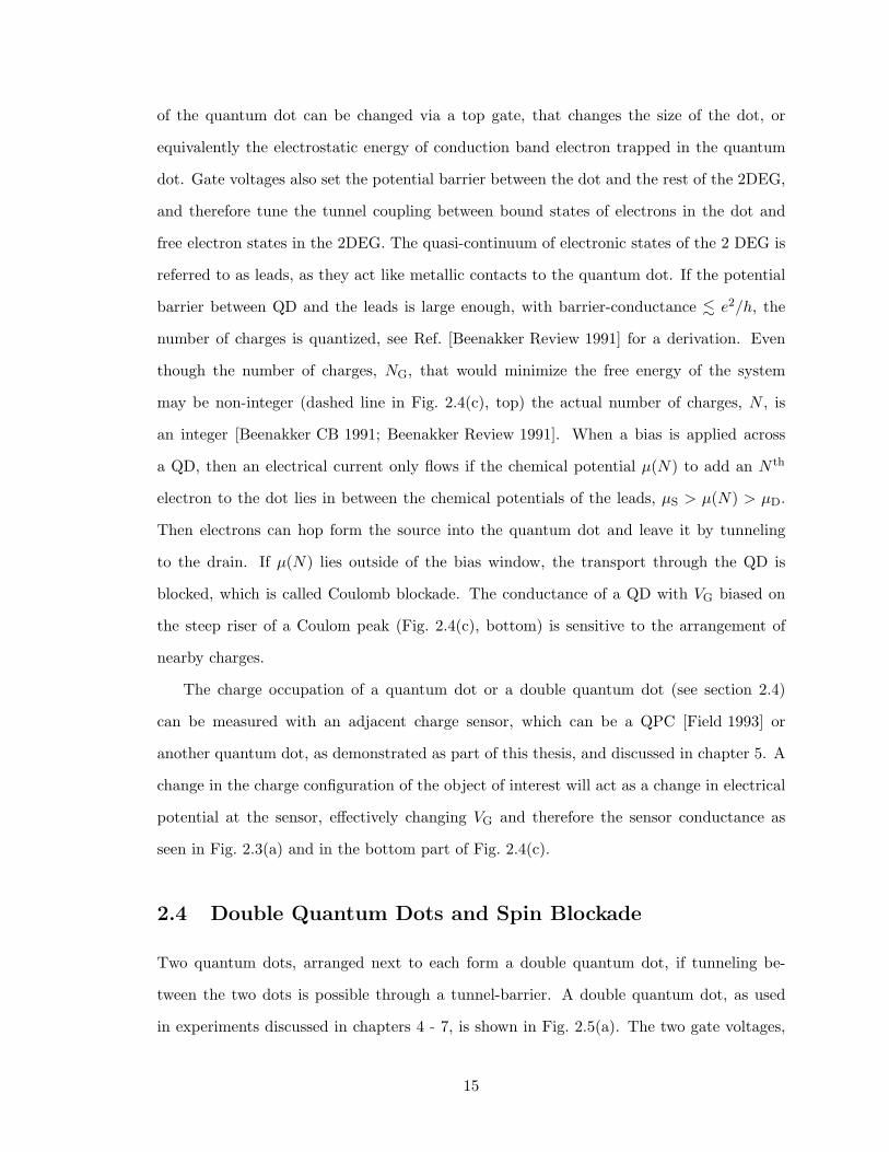
Two quantum dots, arranged next to each form a double quantum dot, if tunneling be-
tween the two dots is possible through a tunnel-barrier. A double quantum dot, as used
in experiments discussed in chapters 4 - 7, is shown in Fig. 2.5(a). The two gate voltages,
15
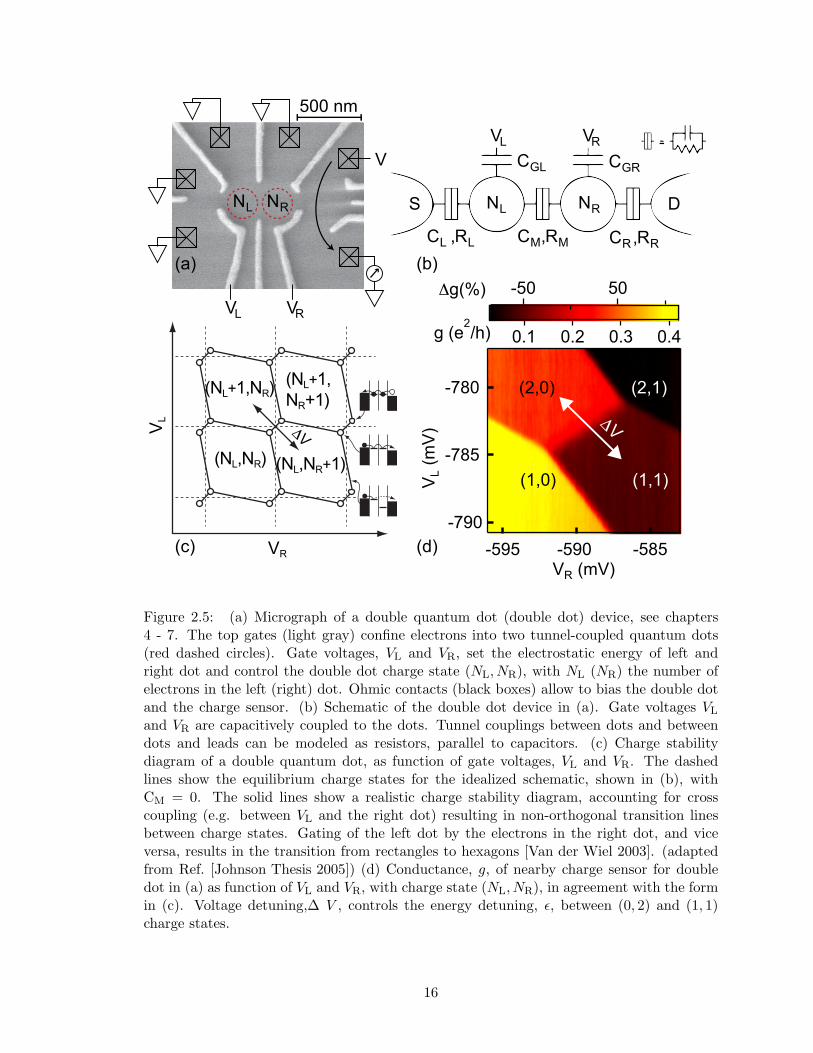
VL VR
500 nm
V
NL NR
Network of tunnel resistors and capacitors represent-
Network of tunnel resistors and capacitors represent-
VL VR
NL NRS D
CGL CGR
CM RM,CL RL, CR RR,
VV
sg1
sC Rs
C
a
ddC R
g1 C
C Rmm
g2
g2
VVs
QD1 QD2 (n+1, m+1)
(n+1, m)
(n, m+1)
(n, m)
1 n+1,m+1 -|e|Vn+1,m+1 01
(n, m) (n+1, m)
(n, m+1)
n+1,m+1 02
E
E
E 2|t|n,m+1
n+1,m
V
E.S.
G.S.
b
c d
V g2
Vg1
A
V
(n+1, m+1)
V g2
Vg1
Figure 3.3: Double quantum dots. a) Circuit equivalent of a double dot. The doubleboxes represent a capacitor and resistor in parallel. b) At zero source-drain bias,the ground state charge is constant within hexagonal regions in the Vg1–Vg2 plane.Ordered pairs (n, m) denote charge on the left and right dots respectively. Currentcan only flow at the vertices, called triple points, where three charge states are inequillibrium. The upper one (top diagram) is called the hole triple point and thelower one (middle diagram) the electron triple point. When the dots are fairly open,conduction is sometimes seen along the hexagon edges as well, due to cotunnelingprocesses as in the bottom diagram. When considering two states of the same totalcharge, e.g. (n, m + 1) and (n + 1, m), the relevant parameter is detuning, or motionaway from equal energy such as the line labeled ∆V . c) At finite source-drain bias,the triple points expand into triangles. Ground-state-to-ground-state transport occursalong the base of each triangle (∆V = 0), and excited states are manifest as lines ofcurrent parallel to the ground state line. d) Due to a finite tunnel coupling t betweenthe dots, two states of the same total charge will hybridize, displaying an avoidedcrossing as a function of detuning. Figure adapted from [40] and [56].
29
VR
VL
(NL,NR)
(NL+1,NR)
(NL,NR+1)
(NL+1,NR+1)
V
(2,0)
(1,1)(1,0)
(2,1)
(a) (b)
(c) (d)
V
Figure 2.5: (a) Micrograph of a double quantum dot (double dot) device, see chapters4 - 7. The top gates (light gray) confine electrons into two tunnel-coupled quantum dots(red dashed circles). Gate voltages, VL and VR, set the electrostatic energy of left andright dot and control the double dot charge state (NL, NR), with NL (NR) the number ofelectrons in the left (right) dot. Ohmic contacts (black boxes) allow to bias the double dotand the charge sensor. (b) Schematic of the double dot device in (a). Gate voltages VL
and VR are capacitively coupled to the dots. Tunnel couplings between dots and betweendots and leads can be modeled as resistors, parallel to capacitors. (c) Charge stabilitydiagram of a double quantum dot, as function of gate voltages, VL and VR. The dashedlines show the equilibrium charge states for the idealized schematic, shown in (b), withCM = 0. The solid lines show a realistic charge stability diagram, accounting for crosscoupling (e.g. between VL and the right dot) resulting in non-orthogonal transition linesbetween charge states. Gating of the left dot by the electrons in the right dot, and viceversa, results in the transition from rectangles to hexagons [Van der Wiel 2003]. (adaptedfrom Ref. [Johnson Thesis 2005]) (d) Conductance, g, of nearby charge sensor for doubledot in (a) as function of VL and VR, with charge state (NL, NR), in agreement with the formin (c). Voltage detuning,∆ V , controls the energy detuning, , between (0, 2) and (1, 1)charge states.
16
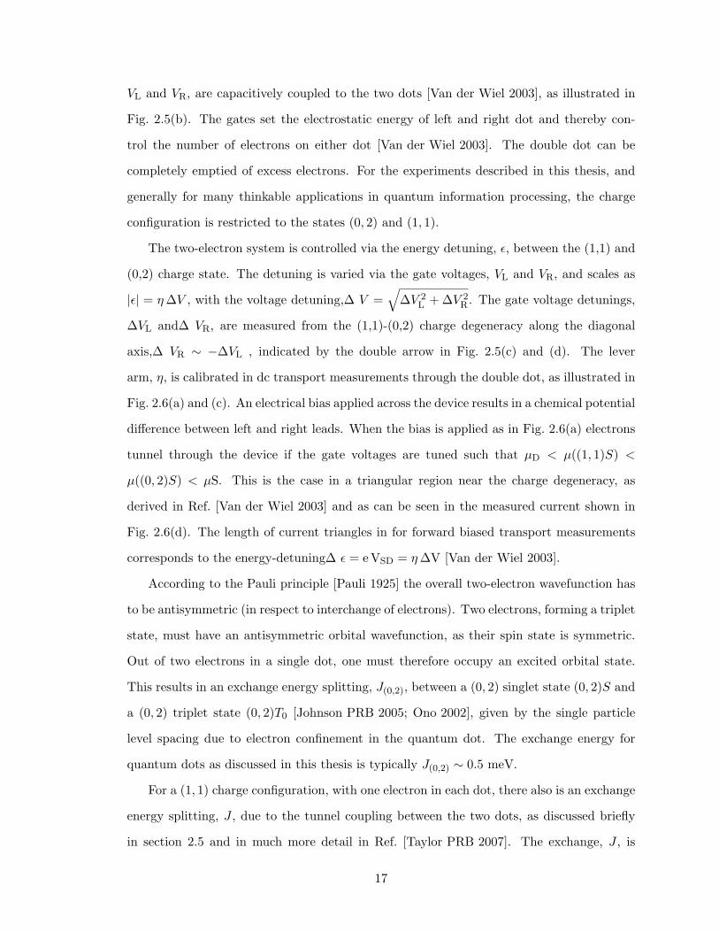
VL and VR, are capacitively coupled to the two dots [Van der Wiel 2003], as illustrated in
Fig. 2.5(b). The gates set the electrostatic energy of left and right dot and thereby con-
trol the number of electrons on either dot [Van der Wiel 2003]. The double dot can be
completely emptied of excess electrons. For the experiments described in this thesis, and
generally for many thinkable applications in quantum information processing, the charge
configuration is restricted to the states (0, 2) and (1, 1).
The two-electron system is controlled via the energy detuning, , between the (1,1) and
(0,2) charge state. The detuning is varied via the gate voltages, VL and VR, and scales as
|| = η ∆V , with the voltage detuning,∆ V =
∆V 2L + ∆V 2
R . The gate voltage detunings,
∆VL and∆ VR, are measured from the (1,1)-(0,2) charge degeneracy along the diagonal
axis,∆ VR ∼ −∆VL , indicated by the double arrow in Fig. 2.5(c) and (d). The lever
arm, η, is calibrated in dc transport measurements through the double dot, as illustrated in
Fig. 2.6(a) and (c). An electrical bias applied across the device results in a chemical potential
difference between left and right leads. When the bias is applied as in Fig. 2.6(a) electrons
tunnel through the device if the gate voltages are tuned such that µD < µ((1, 1)S) <
µ((0, 2)S) < µS. This is the case in a triangular region near the charge degeneracy, as
derived in Ref. [Van der Wiel 2003] and as can be seen in the measured current shown in
Fig. 2.6(d). The length of current triangles in for forward biased transport measurements
corresponds to the energy-detuning∆ = e VSD = η ∆V [Van der Wiel 2003].
According to the Pauli principle [Pauli 1925] the overall two-electron wavefunction has
to be antisymmetric (in respect to interchange of electrons). Two electrons, forming a triplet
state, must have an antisymmetric orbital wavefunction, as their spin state is symmetric.
Out of two electrons in a single dot, one must therefore occupy an excited orbital state.
This results in an exchange energy splitting, J(0,2), between a (0, 2) singlet state (0, 2)S and
a (0, 2) triplet state (0, 2)T0 [Johnson PRB 2005; Ono 2002], given by the single particle
level spacing due to electron confinement in the quantum dot. The exchange energy for
quantum dots as discussed in this thesis is typically J(0,2) ∼ 0.5 meV.
For a (1, 1) charge configuration, with one electron in each dot, there also is an exchange
energy splitting, J , due to the tunnel coupling between the two dots, as discussed briefly
in section 2.5 and in much more detail in Ref. [Taylor PRB 2007]. The exchange, J , is
17
sdeVS
T
-1.035
-1.025
100
-1.04
-1.03
-0.96 -0.95V2 (V)
(0,1)
(1,1)
(0,2)
(1,2)
V 6 (V
)V 6
(V)
gs (10-3 e2/h)
e)
f)
-1.035
-1.025
151050
-1.04
-1.03
V 6 (V
)-0.96 -0.95
V 6 (V
)V2 (V)
c)
d)
(0,1)
(1,1)
(0,2)
(1,2)
I| d | (pA)J02
sdV = +0.5 mV
sdV = -0.5 mV
sdV = +0.5 mV
sdV = -0.5 mV
a)
b) Singlet Triplet
Figure 1.4: Spin blockade in a double quantum dot. (a) Chemical potential of dots and leadsunder positive bias Vsd. The triplet state of the right dot is higher in energy by the exchangeJ02, but this does not prevent electron transport through the device. (b) Under negativebias, exchange makes electron tunneling spin-selective, suppressing transport. (c) and (d)Current Id through the device for positive and negative bias, showing strong asymmetry.(e) and (f) Charge sensing signal, also showing asymmetry [31].
1.4 Double quantum dots and spin blockade
A richer and more tunable spectrum of electron states can be achieved in double quantum
dots (Fig. 1.3(a)) [29]. To some extent, the properties of each dot can be tuned separately.
The occupations (NL, NR) of left and right dots respectively are controlled mainly by the
gate voltages VL and VR, resulting in the charge stability diagram shown in Fig. 1.3(b) [30,
28]. Small enough devices can be completely emptied, allowing precise control of the number
of electrons in each dot.
One of the most important features of double dots from the point of view of spin physics
is that the exchange between two electrons occupying the device can be tuned over a very
wide range. The exchange, defined as the energy difference between the lowest ms = 0spin-
triplet and spin-singlet levels, arises because Pauli exclusion requires overall antisymmetry
8
Singlet Triplet
T
SVSD
J(0,2)
D
S
D
S
D
S
-700
-690
VL (
mV
)
-870 -860VR (mV)
-1.0
-0.5
0.0IS
D (pA)
-700
-690
VL (
mV
)
-875 -870 -865VR (mV)
1.0
0.5
0.0
ISD (pA
)
VL VR500 nm
NL NR
VSD
ISD (d)
(f)
(a)
(b)
(c)
(0,2)
(1,1)(0,1)
(2,1)
(0,2)
(1,1)(0,1)
(2,1)
VSD=300 V
VSD=-300 V
Figure 2.6: DC transport and spin blockade (a) With a forward bias [VSD > 0 for setupshown in (c)] applied, electrons can successively tunnel through the two dots, because the(0, 2) singlet state is loaded, and tunnels into the (1, 1) singlet. (b) With a reverse bias[VSD < 0 for setup shown in (c)] applied, a (1, 1)S state that is formed by an electron tun-neling in from the leads, can tunnel through the (0,2) charge state. However, if the loadedelectron forms a triplet state with the electron already in the double dot, tunneling is forbid-den, as the (0, 2) triplet state is not energetically accessible, and transport is spin-blockaded.(a) and (b) are adapted from Ref. [Laird 2009]. (c) Setup to measure spin blockade with theelectron configuration (NL, NR) at the (1, 1)-(0, 2) degeneracy, a bias VSD is applied acrossthe double dot, and the current ISD is measured. (d) Current, ISD, through the doubledot, biased in forward direction. In the transport triangles a roughly homogenous currentflows [Van der Wiel 2003]. (e) For a double dot in reverse bias [VSD < 0 for setup shown in(c)] , the current flow through the bias triangles is strongly suppressed [Johnson PRB 2005].The lines of current are due to formed triplet states transitioning into singlet states by vir-tual electron exchange with the leads [Johnson PRB 2005].
typically much smaller than J(0,2), see Fig. 2.6(a), and can be made arbitrarily small via
choice of gate voltages.
Spin blockade is illustrated and the singlet triplet splitting can be measured by applying
a reverse bias across the double dot, as illustrated in Fig. 2.6(b), with the setup shown in
Fig. 2.6(c). The chemical potential to load a singlet or a triplet state into the (1, 1) charge
configuration is practically identical, compared to other energy scales. If the electron loaded
into the left dot forms a triplet state with the electron in the right dot, it cannot tunnel
into the right dot because tunneling conserves electron spin and the (0, 2) triplet state is
18
energetically inaccessible. Due to the bias it cannot escape back to the left lead either and
electron transport stops until a spin flip occurs, yielding a an almost zero average current
through the double dot. The current ISD is shown as function of the gate voltages∆ VL and
∆VR for a reverse bias, VSD = −300 µeV in Fig. 2.6(e). For a reverse bias there is no current
flowing in the transport triangles. The current along the lines bordering the triangle is due
to co-tunneling, electron spin flips due to virtual electron exchange with the leads. When
a sufficiently large bias, eVSD > J(0,2), is applied current starts flowing at the tip of the
transport triangle. This allows to measure J(0,2) in a dc-measurement [Johnson PRB 2005;
Van der Wiel 2003], analogous to the measurement for the lever-arm with forward bias,
discussed above.
2.5 Coherent Manipulation and Decoherence of Singlet-Triplet
Spin Qubits
The qubit, on which chapters 4 - 7 are focussing, is formed by the singlet-triplet basis of a
pair of electron spins in a double quantum dot [Levy 2002], see section 2.1.2. As discussed
in section 2.4, two electrons can be trapped in a double dot, and the energy detuning, ,
between the charge states (0, 2) and (1, 1) of the double dot can be controlled via the gate
voltage detuning,∆ V , as illustrated in Fig. 2.5(c), (d). The energy detuning can also be
used to control and manipulate the spin state of the two electrons, thanks to the Pauli
principle which leads to an influence of the spin-state on the orbital wave function and
charge state, and vice versa.
To understand the singlet-triplet qubit, its proposed operation and the experiments
discussed in the following, it is instructive to consider the energy level diagram as a function
of detuning, , shown in Fig. 2.7. The singlet states of (0, 2) and (1, 1) anti-cross at = 0,
because an increase in energy detuning makes it more favorable for the two electrons to
occupy one dot. For two electrons occupying one dot, there is a large exchange energy
splitting J(0,2) between singlet and triplet states (0, 2)S and (0, 2)T−,0,+. Thus the charging
energy must compensate for this, by making the occupation of a single dot more favorable,
compared to a singlet, in order to load a (0, 2) triplet state. The anti-crossing between the
19
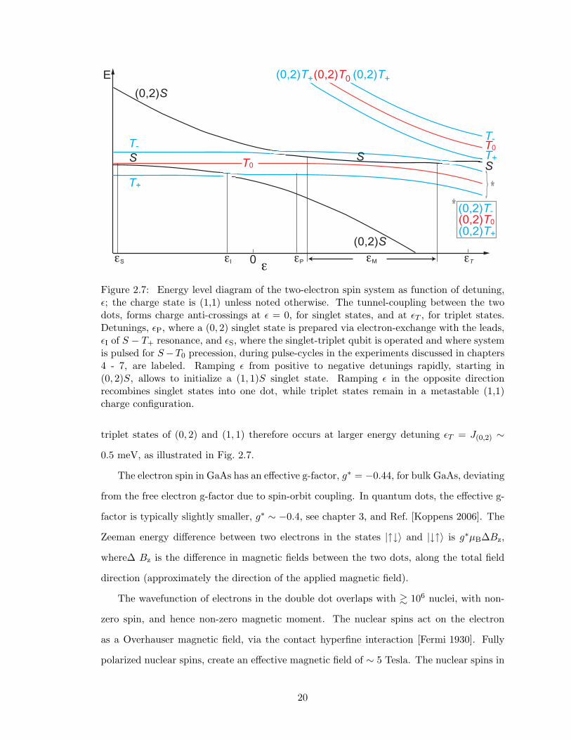
E
T-
0
(0,2)S
(0,2)S
T+
T0
S MI P T
SS
(0,2)T0 (0,2)T+(0,2)T+
T-
T+T0
S
(0,2)T0(0,2)T+
(0,2)T-
**
Figure 2.7: Energy level diagram of the two-electron spin system as function of detuning,; the charge state is (1,1) unless noted otherwise. The tunnel-coupling between the twodots, forms charge anti-crossings at = 0, for singlet states, and at T , for triplet states.Detunings, P, where a (0, 2) singlet state is prepared via electron-exchange with the leads,I of S − T+ resonance, and S, where the singlet-triplet qubit is operated and where systemis pulsed for S−T0 precession, during pulse-cycles in the experiments discussed in chapters4 - 7, are labeled. Ramping from positive to negative detunings rapidly, starting in(0, 2)S, allows to initialize a (1, 1)S singlet state. Ramping in the opposite directionrecombines singlet states into one dot, while triplet states remain in a metastable (1,1)charge configuration.
triplet states of (0, 2) and (1, 1) therefore occurs at larger energy detuning T = J(0,2) ∼
0.5 meV, as illustrated in Fig. 2.7.
The electron spin in GaAs has an effective g-factor, g∗ = −0.44, for bulk GaAs, deviating
from the free electron g-factor due to spin-orbit coupling. In quantum dots, the effective g-
factor is typically slightly smaller, g∗ ∼ −0.4, see chapter 3, and Ref. [Koppens 2006]. The
Zeeman energy difference between two electrons in the states |↑↓ and |↓↑ is g∗µB∆Bz,
where∆ Bz is the difference in magnetic fields between the two dots, along the total field
direction (approximately the direction of the applied magnetic field).
The wavefunction of electrons in the double dot overlaps with 106 nuclei, with non-
zero spin, and hence non-zero magnetic moment. The nuclear spins act on the electron
as a Overhauser magnetic field, via the contact hyperfine interaction [Fermi 1930]. Fully
polarized nuclear spins, create an effective magnetic field of ∼ 5 Tesla. The nuclear spins in
20
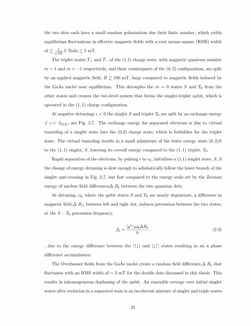
the two dots each have a small random polarization due their finite number, which yields
equilibrium fluctuations in effective magnetic fields with a root means square (RMS) width
of 1√106
5 Tesla 5 mT.
The triplet states T+ and T− of the (1,1) charge state, with magnetic quantum number
m = 1 and m = −1 respectively, and their counterparts of the (0, 2) configuration, are split
by an applied magnetic field, B 100 mT, large compared to magnetic fields induced by
the GaAs nuclei near equilibrium. This decouples the m = 0 states S and T0 from the
other states and creates the two-level system that forms the singlet-triplet qubit, which is
operated in the (1, 1) charge configuration.
At negative detunings < 0 the singlet S and triplet T0 are split by an exchange energy
J << J(0,2), see Fig. 2.7. The exchange energy for separated electrons is due to virtual
tunneling of a singlet state into the (0,2) charge state, which is forbidden for the triplet
state. The virtual tunneling results in a small admixture of the lower energy state (0, 2)S
to the (1, 1) singlet, S, lowering its overall energy compared to the (1, 1) triplet, T0.
Rapid separation of the electrons, by pulsing to S, initializes a (1,1) singlet state, S, if
the change of energy detuning is slow enough to adiabatically follow the lower branch of the
singlet anti-crossing in Fig. 2.7, but fast compared to the energy scale set by the Zeeman
energy of nuclear field differences∆ Bz between the two quantum dots.
At detuning, S, where the qubit states S and T0 are nearly degenerate, a difference in
magnetic field,∆ Bz, between left and right dot, induces precession between the two states,
at the S − T0 precession frequency,
fS =|g∗|µB∆Bz
h. (2.3)
, due to the energy difference between the |↑↓ and |↓↑ states resulting in an a phase
difference accumulation.
The Overhauser fields from the GaAs nuclei create a random field difference,∆ Bz that
fluctuates with an RMS width of ∼ 2 mT for the double dots discussed in this thesis. This
results in inhomogeneous dephasing of the qubit. An ensemble average over initial singlet
states after evolution in a separated state is an incoherent mixture of singlet and triple states
21
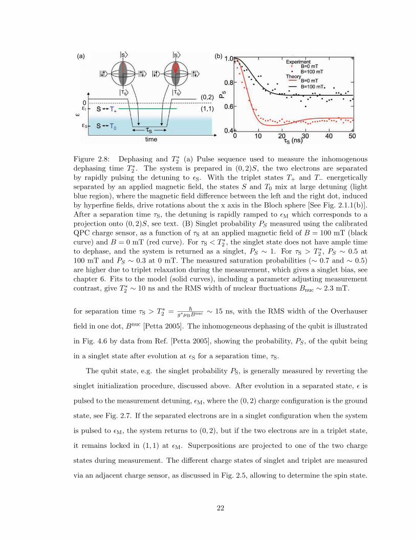
(0,2)
(1,1)
time
0I
S
(a) (b)
Figure 2.8: Dephasing and T ∗2 (a) Pulse sequence used to measure the inhomogenous
dephasing time T ∗2 . The system is prepared in (0, 2)S, the two electrons are separated
by rapidly pulsing the detuning to S. With the triplet states T+ and T− energeticallyseparated by an applied magnetic field, the states S and T0 mix at large detuning (lightblue region), where the magnetic field difference between the left and the right dot, inducedby hyperfine fields, drive rotations about the x axis in the Bloch sphere [See Fig. 2.1.1(b)].After a separation time τS, the detuning is rapidly ramped to M which corresponds to aprojection onto (0, 2)S, see text. (B) Singlet probability PS measured using the calibratedQPC charge sensor, as a function of τS at an applied magnetic field of B = 100 mT (blackcurve) and B = 0 mT (red curve). For τS < T ∗
2 , the singlet state does not have ample timeto dephase, and the system is returned as a singlet, PS ∼ 1. For τS > T ∗
2 , PS ∼ 0.5 at100 mT and PS ∼ 0.3 at 0 mT. The measured saturation probabilities (∼ 0.7 and ∼ 0.5)are higher due to triplet relaxation during the measurement, which gives a singlet bias, seechapter 6. Fits to the model (solid curves), including a parameter adjusting measurementcontrast, give T ∗
2 ∼ 10 ns and the RMS width of nuclear fluctuations Bnuc ∼ 2.3 mT.
for separation time τS > T ∗2 =
g∗µBBnuc ∼ 15 ns, with the RMS width of the Overhauser
field in one dot, Bnuc [Petta 2005]. The inhomogeneous dephasing of the qubit is illustrated
in Fig. 4.6 by data from Ref. [Petta 2005], showing the probability, PS , of the qubit being
in a singlet state after evolution at S for a separation time, τS.
The qubit state, e.g. the singlet probability PS, is generally measured by reverting the
singlet initialization procedure, discussed above. After evolution in a separated state, is
pulsed to the measurement detuning, M, where the (0, 2) charge configuration is the ground
state, see Fig. 2.7. If the separated electrons are in a singlet configuration when the system
is pulsed to M, the system returns to (0, 2), but if the two electrons are in a triplet state,
it remains locked in (1, 1) at M. Superpositions are projected to one of the two charge
states during measurement. The different charge states of singlet and triplet are measured
via an adjacent charge sensor, as discussed in Fig. 2.5, allowing to determine the spin state.
22
Generally, many experimental cycles of singlet separation, evolution and recombination
for spin-to-charge conversion are performed and the charge signal is averaged, yielding an
ensemble averaged singlet probability [Petta 2005]. Chapter 4 discusses the implementation
of single-shot qubit measurement for the singlet-triplet spin qubit [Barthel 2009].
In order to initialize the qubit in a state | X rather than | Z, a slow sweep of from
I to S, maps a (1, 1) singlet, S = (|↑↓− |↓↑) /√
2, onto the ground state of the
nuclear Overhauser fields, |↑↓ [Petta 2005], as illustrated in Fig. 2.9(a). This allows to
demonstrate fast z-axis rotation, driven by the exchange energy splitting, J , due to a phase
accumulation between S and T0.
After initialization into |↑↓, is pulsed to E, with an exchange energy, JE > |g∗|µB∆Bz,
larger (ideally much larger) than the nuclear field gradient [Petta 2005; Foletti 2009]. This
results in rapid precession around the z-axis of the qubit Bloch sphere as demonstrated
in Ref. [Petta 2005] and shown in Fig. 2.9(b) and (c). The oscillations are detected by
measuring the x-axis projection of the qubit as function of the exchange evolution time, τE
(Fig. 2.9).
The projection of the qubit on the x-axis, or equivalently onto state |↑↓ , is measured,
by reverting the initialization procedure of state | X =|↑↓. The detuning is slowly ramped
from S to I, mapping the state |↑↓ onto the (1, 1) singlet state. The state |↓↑ is
mapped onto T0. This state mapping is followed by a rapid pulse to M to measure the singlet
probability, PS, via the double dot charge state, using the charge sensor. The measured
singlet probability, shown in Fig. 2.9(b), corresponds to the | X probability, p(| X), before
the mapping. In Ref. [Petta 2005] oscillation periods shorter than one nanoseconds were
realized, the operation time for z-rotations is practically only limited by pulse rise-times.
Qubit rotations around a second independent axis are needed for universal control of the
singlet-triplet qubit in order for it to be a viable system for quantum information processing.
As discussed above, an x-rotation is induced by a magnetic field difference,∆ Bz between
the two quantum dots. A field difference for these rotations can be realized via a micro
magnet on top of the double dot as experimentally shown in Ref. [Pioro-Ladriere 2007] and
in Refs. [Laird 2007; Laird 2009] as part of this thesis, discussed in chapter 3.
Recently a nuclear field difference between two dots in a double dot has been realized
23
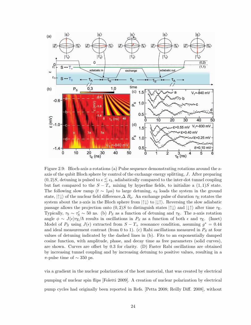
time
0I
S
(a)
(b)(c)
(d)
Figure 2.9: Bloch-axis z-rotations (a) Pulse sequence demonstrating rotations around the z-axis of the qubit Bloch sphere by control of the exchange energy splitting, J . After preparing(0, 2)S, detuning is pulsed to I, adiabatically compared to the inter-dot tunnel couplingbut fast compared to the S − T+ mixing by hyperfine fields, to initialize a (1, 1)S state.The following slow ramp (t ∼ 1µs) to large detuning, S loads the system in the groundstate, |↑↓ of the nuclear field difference,∆ Bz. An exchange pulse of duration τE rotates thesystem about the z-axis in the Bloch sphere from |↑↓ to |↓↑. Reversing the slow adiabaticpassage allows the projection onto (0, 2)S to distinguish states |↑↓ and |↓↑ after time τE.Typically, τS ∼ τ S ∼ 50 ns. (b) PS as a function of detuning and τE. The z-axis rotationangle φ ∼ J()τE/ results in oscillations in PS as a function of both and τE. (Inset)Model of PS using J() extracted from S − T+ resonance condition, assuming g∗ = 0.44and ideal measurement contrast (from 0 to 1). (c) Rabi oscillations measured in PS at fourvalues of detuning indicated by the dashed lines in (b). Fits to an exponentially dampedcosine function, with amplitude, phase, and decay time as free parameters (solid curves),are shown. Curves are offset by 0.3 for clarity. (D) Faster Rabi oscillations are obtainedby increasing tunnel coupling and by increasing detuning to positive values, resulting in aπ-pulse time of ∼ 350 ps.
via a gradient in the nuclear polarization of the host material, that was created by electrical
pumping of nuclear spin flips [Foletti 2009]. A creation of nuclear polarization by electrical
pump cycles had originally been reported in Refs. [Petta 2008; Reilly Diff. 2008], without
24
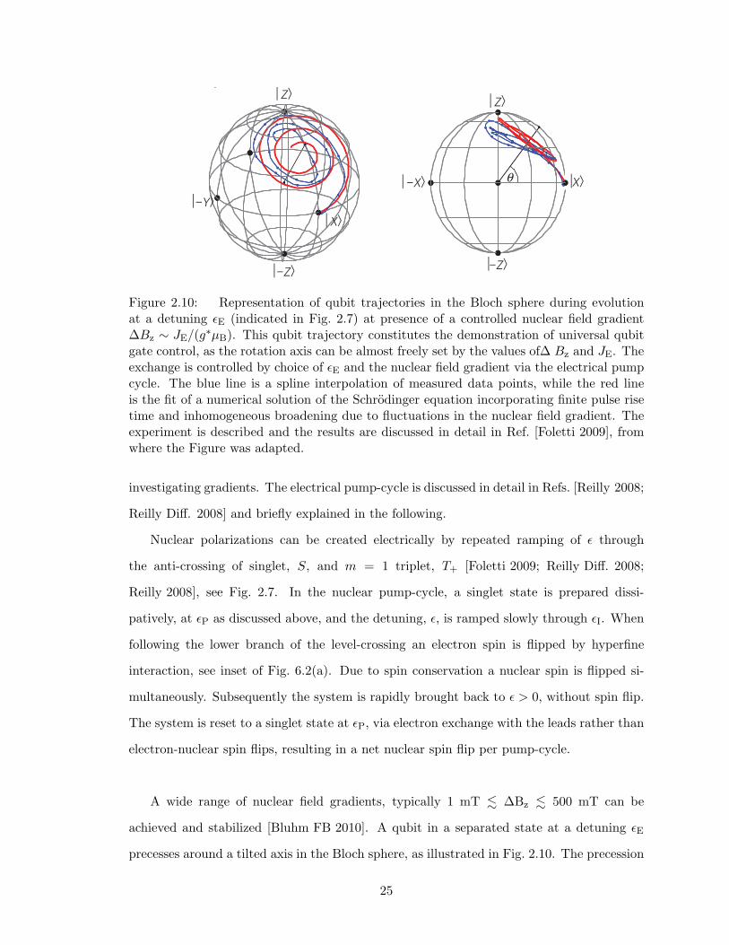
ARTICLES NATURE PHYSICS DOI: 10.1038/NPHYS1424
PreparationZ
X-readoutcddd e
Y-readout
0.4
0.6
0.8
1.0
0.2
0.8
X
Y
Z
t
rot
rot
rot (ns)
rot
/2¬pulse
M
S¬T+
S
t
t
M
M
S¬T+
S¬T+
S
S
0
0
0
p(X
)p(
Y)
p(Z
)
0.3
1
0 10 20 30
rot (ns)0 10 20 30
rot (ns)0 10 20 30
X ¬X
X
X
X
Y
¬Y
¬Z
Z
¬Z
ZZ
Z
a b
Figure 4 | State tomography and universal gate. a, Pulse schemes used to measure the singlet probability p(|S〉)≡ p(|Z〉), the |↑↓〉 probabilityp(|↑↓〉)≡ p(|X〉) and the |S〉+ i|T0〉 probability p(|S〉+ i|T0〉)≡ p(|Y〉) after rotation around a tilted, tunable axis. b, Measurements taken with the X, Y andZ pulses (dots) and fits (line) to a numerical solution of the Schrödinger equation of the S–T0 Hamiltonian incorporating the finite pulse rise time andinhomogeneous broadening owing to fluctuations in !Bznuc. c, A |↑↓〉= |X〉 state is prepared by adiabatically turning off J. d, Representation of themeasured and fitted trajectories in the Bloch sphere. To eliminate phase shifts owing to the slightly different frequencies (see text), the timescales for theX-data have been rescaled using spline interpolation so that the expected phase relations are maintained. The blue line is a spline interpolation of the datapoints in b. e, Visualization of the X and Y-readout schemes on the Bloch sphere.
interaction. Here, we present two polarization schemes by whichthe gradient can be increased to values significantly exceeding itsfluctuations. Both pumping schemes make use of the degeneracypoint between S(1,1) and T+. Transitions between the two statesthat are driven by the transverse component of !Bnuc (ref. 15)are accompanied by a spin flip of the nuclei to conserve the totalangular momentum. Our first pumping scheme follows a standardrecipe16,17 of initializing the system in the S(0,2) state followed bya 50- or 100-ns-long sweep across the S–T+ degeneracy point. Thisprocess ideally transfers one unit of angular momentum into thenuclear subsystem. In addition, we have developed an alternativepumping scheme,wherebywe initialize the system in aT+(1,1) statefollowed by a similar slow passage through the S–T+ degeneracypoint. This new T+-pumping scheme allows us to polarize thenuclear subsystem in a direction opposite to the S-pumping scheme.The T+-pumping scheme works only when the Zeeman energyexceeds the electron temperature in the reservoirs: the system isswept slowly into (0, 1) and subsequently reloaded into the (1, 1)charge state (Fig. 1e). First the right and then the left electron alignwith the external field because of large Zeeman energy (≈12.5 µeVat 500mT), which preferentially loads a T+ state.
Although the above nuclear pumping schemes should producenuclear polarization, it is not obvious at all that this nuclearpolarization should be different across the two dots17. As themixing between the S(1,1) and T0 (1, 1) is sensitive only to thefield gradient, we use a pulse cycle that monitors the coherentevolution around the x axis to measure this gradient. The systemis first reset into a S(0, 2) state. ε is then abruptly set topoint S in (1, 1) for an evolution time τS (see Fig. 1g). Here,!Bz
nuc & J (ε)/gµB drives coherent oscillations between S(1,1)and T0 and the probability of being in a singlet state oscillatesin time as p(S) = cos2(gµB!Bz
nuc · τS/2h). When the system isbrought back to the measurement point M, only transitions fromS(1,1) to S(0,2) are allowed, whereas T0 remains blocked inthe (1, 1) charge configuration. This spin-blockade effect allowsmapping of the spin configuration of the state onto a chargeconfiguration18, which is measured by a charge sensor18. Here,we use a quantum point contact (QPC) positioned next to thedouble quantum dot (Fig. 1b) to detect changes in the double-dot charge configuration. The QPC signal, averaged over manygradient-probing cycles, is proportional to the probability ofbeing in a singlet state.
906 NATURE PHYSICS | VOL 5 | DECEMBER 2009 | www.nature.com/naturephysics
Figure 2.10: Representation of qubit trajectories in the Bloch sphere during evolutionat a detuning E (indicated in Fig. 2.7) at presence of a controlled nuclear field gradient∆Bz ∼ JE/(g∗µB). This qubit trajectory constitutes the demonstration of universal qubitgate control, as the rotation axis can be almost freely set by the values of∆ Bz and JE. Theexchange is controlled by choice of E and the nuclear field gradient via the electrical pumpcycle. The blue line is a spline interpolation of measured data points, while the red lineis the fit of a numerical solution of the Schrodinger equation incorporating finite pulse risetime and inhomogeneous broadening due to fluctuations in the nuclear field gradient. Theexperiment is described and the results are discussed in detail in Ref. [Foletti 2009], fromwhere the Figure was adapted.
investigating gradients. The electrical pump-cycle is discussed in detail in Refs. [Reilly 2008;
Reilly Diff. 2008] and briefly explained in the following.
Nuclear polarizations can be created electrically by repeated ramping of through
the anti-crossing of singlet, S, and m = 1 triplet, T+ [Foletti 2009; Reilly Diff. 2008;
Reilly 2008], see Fig. 2.7. In the nuclear pump-cycle, a singlet state is prepared dissi-
patively, at P as discussed above, and the detuning, , is ramped slowly through I. When
following the lower branch of the level-crossing an electron spin is flipped by hyperfine
interaction, see inset of Fig. 6.2(a). Due to spin conservation a nuclear spin is flipped si-
multaneously. Subsequently the system is rapidly brought back to > 0, without spin flip.
The system is reset to a singlet state at P, via electron exchange with the leads rather than
electron-nuclear spin flips, resulting in a net nuclear spin flip per pump-cycle.
A wide range of nuclear field gradients, typically 1 mT ∆Bz 500 mT can be
achieved and stabilized [Bluhm FB 2010]. A qubit in a separated state at a detuning E
precesses around a tilted axis in the Bloch sphere, as illustrated in Fig. 2.10. The precession
25
frequency
fE =
J2
E + (g∗µB∆Bz)2
h(2.4)
and the rotation axis in the Bloch sphere (Fig. 2.10) are set by exchange energy and magnetic
field difference which can be controlled via the detuning E and the nuclear pump cycle.
This rotation around an arbitrary axis on the Bloch sphere constitutes the realization of
universal control of the qubit state.
Aside from being a useful tool to manipulate the qubit, the Overhauser fields of the nuclei
also are the major source of qubit decoherence as discussed above (Fig. 4.6 [Petta 2005]).
However the fluctuations of nuclear fields have been shown to be slow and to have a ∼
1/f2 power spectrum at moderate to high applied magnetic fields [Reilly 2007]. Dephasing
can be partially undone by a spin echo, a π-rotation on the bloch sphere, that refocusses
the evolution of the electron spin state [Hahn 1950; Petta 2005; Bluhm T2 2010]. The π-
rotations are realized via z-rotations by pulsing the system to detuning E for half an
oscillation period. In a Hahn echo sequence [Hahn 1950], a π-pulse is performed after time
τD/2 spent at S, during which the qubit state precesses out of its initial state. After the
π-rotation the system is rapidly brought back to S for the time τD/2 during which the spin
state precesses back into its original state, if the nuclear field has not changed.
In Refs. [Petta 2005; Bluhm T2 2010] a Hahn echo was used to extend the qubit co-
herence time from T ∗2 of few nanoseconds up to ∼ 30 µs. Multiple π- pulses extend the
coherence to longer times, as suggested in Refs. [Carr 1954; Meiboom 1958] and experimen-
tally demonstrated in Ref. [Bluhm T2 2010]. For the Carr Purcell spin echo sequence, Nπ
π-pulses are performed, each with an equal dephasing and rephasing time, before and after
the π-pulse [Carr 1954; Meiboom 1958]. Theoretical work suggests that, under the assump-
tions of certain dephasing power spectra, spin echo sequences more complex than CP could
further increase coherence times. [Witzel CDD 2007; Uhrig 2007] In chapter 7 experiments
that interlace operations around x- or z-axis of the Bloch sphere with Carr Purcell spin
echoes, and experiments that compare different spin echo pulse sequences are discussed.
Therefore the requirements for single qubit operation [DiVincenzo 1998], fast measure-
ment, initialization, universal control and long coherence times have been implemented,
26
while not simultaneously in a single device during a single experiment. However two-
qubit operations are critical for the realization of a quantum computer [DiVincenzo 1998],
and have not been realized thus far. Promising progress has been made however, the
charge coupling between two adjacent quantum dots has been shown to be strong enough
to in principle allow phase operations on one singlet-triplet qubit, conditional on another
qubit [Laird 2010]. One of the double dots being in the (0,2) versus (1,1) configuration re-
sults in a detuning difference of∆ ∼ 50 µeV in the other double dot [Laird 2010], enough
to create a significant difference in exchange oscillation frequency.
27
Chapter 3
A new Mechanism of electricDipole Spin Resonance: HyperfineCoupling in Quantum Dots
E A Laird1, C Barthel1, E I Rashba1,2, C M Marcus1, M P Hanson3 and A C Gossard3
1 Department of Physics, Harvard University, Cambridge, Massachusetts 02138, USA
2 Center for Nanoscale Systems, Harvard University, Cambridge, Massachusetts 02138, USA
3 Materials Department, University of California at Santa Barbara, Santa Barbara, Cali-
fornia 93106, USA
A recently discovered mechanism of electric dipole spin resonance, mediated by the
hyperfine interaction, is investigated experimentally and theoretically. The effect is studied
using a spin-selective transition in a GaAs double quantum dot. The resonant frequency
is sensitive to the instantaneous hyperfine effective field, revealing a nuclear polarization
created by driving the resonance. A device incorporating a micromagnet exhibits a magnetic
field difference between dots, allowing electrons in either dot to be addressed selectively.
An unexplained additional signal at half the resonant frequency is presented 1.
1This chapter is adapted from Ref. [Laird 2007; Laird 2009] with permission, c(2009) by the AmericanPhysical Society
28
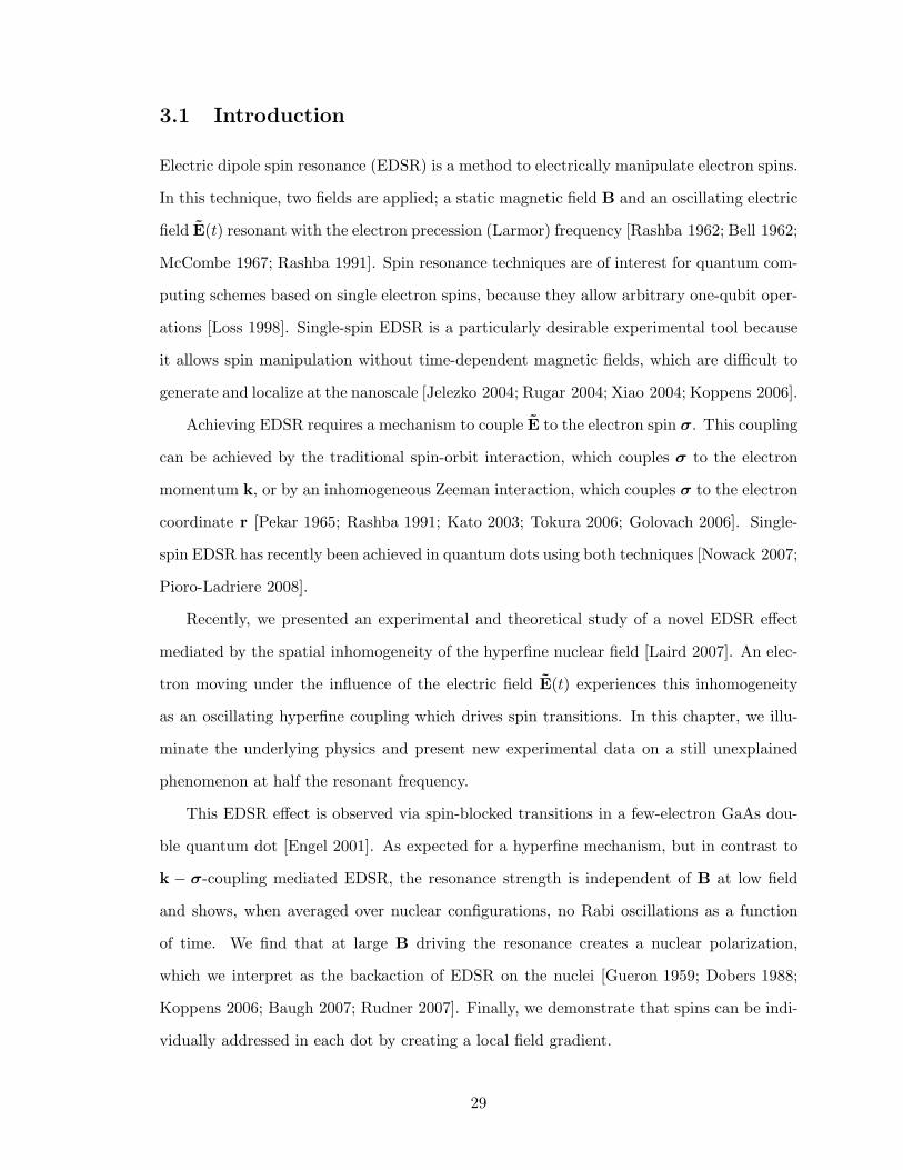
3.1 Introduction
Electric dipole spin resonance (EDSR) is a method to electrically manipulate electron spins.
In this technique, two fields are applied; a static magnetic field B and an oscillating electric
field E(t) resonant with the electron precession (Larmor) frequency [Rashba 1962; Bell 1962;
McCombe 1967; Rashba 1991]. Spin resonance techniques are of interest for quantum com-
puting schemes based on single electron spins, because they allow arbitrary one-qubit oper-
ations [Loss 1998]. Single-spin EDSR is a particularly desirable experimental tool because
it allows spin manipulation without time-dependent magnetic fields, which are difficult to
generate and localize at the nanoscale [Jelezko 2004; Rugar 2004; Xiao 2004; Koppens 2006].
Achieving EDSR requires a mechanism to couple E to the electron spin σ. This coupling
can be achieved by the traditional spin-orbit interaction, which couples σ to the electron
momentum k, or by an inhomogeneous Zeeman interaction, which couples σ to the electron
coordinate r [Pekar 1965; Rashba 1991; Kato 2003; Tokura 2006; Golovach 2006]. Single-
spin EDSR has recently been achieved in quantum dots using both techniques [Nowack 2007;
Pioro-Ladriere 2008].
Recently, we presented an experimental and theoretical study of a novel EDSR effect
mediated by the spatial inhomogeneity of the hyperfine nuclear field [Laird 2007]. An elec-
tron moving under the influence of the electric field E(t) experiences this inhomogeneity
as an oscillating hyperfine coupling which drives spin transitions. In this chapter, we illu-
minate the underlying physics and present new experimental data on a still unexplained
phenomenon at half the resonant frequency.
This EDSR effect is observed via spin-blocked transitions in a few-electron GaAs dou-
ble quantum dot [Engel 2001]. As expected for a hyperfine mechanism, but in contrast to
k − σ-coupling mediated EDSR, the resonance strength is independent of B at low field
and shows, when averaged over nuclear configurations, no Rabi oscillations as a function
of time. We find that at large B driving the resonance creates a nuclear polarization,
which we interpret as the backaction of EDSR on the nuclei [Gueron 1959; Dobers 1988;
Koppens 2006; Baugh 2007; Rudner 2007]. Finally, we demonstrate that spins can be indi-
vidually addressed in each dot by creating a local field gradient.
29
3.2 Device and Measurement
The device for which most data is presented (Figure 1(a)) was fabricated on a GaAs /
Al0.3Ga0.7As heterostructure with two-dimensional electron gas (2DEG) of density 2 ×
1015 m−2 and mobility 20 m2/Vs located 110 nm below the surface. Voltages applied to
Ti/Au top gates locally deplete the 2DEG, defining a few-electron double quantum dot. A
nearby charge sensing quantum point contact (QPC) is sensitive to the electron occupation
(NL, NR) of the left (NL) and right (NR) dots [Field 1993; Elzerman 2003]. The voltages
VL and VR on gates L and R can be rapidly pulsed; in addition, L is coupled to a microwave
source. The static magnetic field B was applied in the plane of the heterostructure, and
measurements were performed in a dilution refrigerator at 150 mK electron temperature.
The characteristic feature of tunnel-coupled quantum dots is a discrete electron energy
spectrum. An overall shift to the spectrum, proportional to the electron occupation, is in-
duced by VL and VR, which therefore determine which occupation is energetically favoured.
Figure 1(b) shows the QPC conductance gs as a function of VL and VR; different conduc-
tances correspond to different (NL, NR). For most VL, VR configurations, only one value of
(NL, NR) is energetically accessible; these correspond in Figure 1(b) to regions of uniform
gs.
A bias Vsd applied across the device drives electron transport via sequential tunneling
subject to two constraints [Hanson 2007]. The first constraint, Coulomb blockade, arises
because for most gate configurations electrostatic repulsion prevents additional electrons
from tunneling onto either dot. This constraint inhibits transport except when VL, VR are
tuned so that three occupation configurations are near-degenerate. The energy cost of an
extra electron tunneling through the device is then small enough to be provided by the bias
voltage. Values of VL and VR satisfying this condition correspond to the two white dashed
triangular regions marked in Figure 1(b), for which transport is permitted via the transition
sequences (0, 2) → (0, 1) → (1, 1) → (0, 2) or (0, 2) → (1, 2) → (1, 1) → (0, 2).
A second constraint, spin blockade, is caused by the Pauli exclusion principle, which
leads to an intra-dot exchange energy J02 in the right dot [Ono 2002; Johnson PRB 2005].
As shown in the first panel of Figure 1(c), the effect of this exchange is to make the (1, 1) →
30
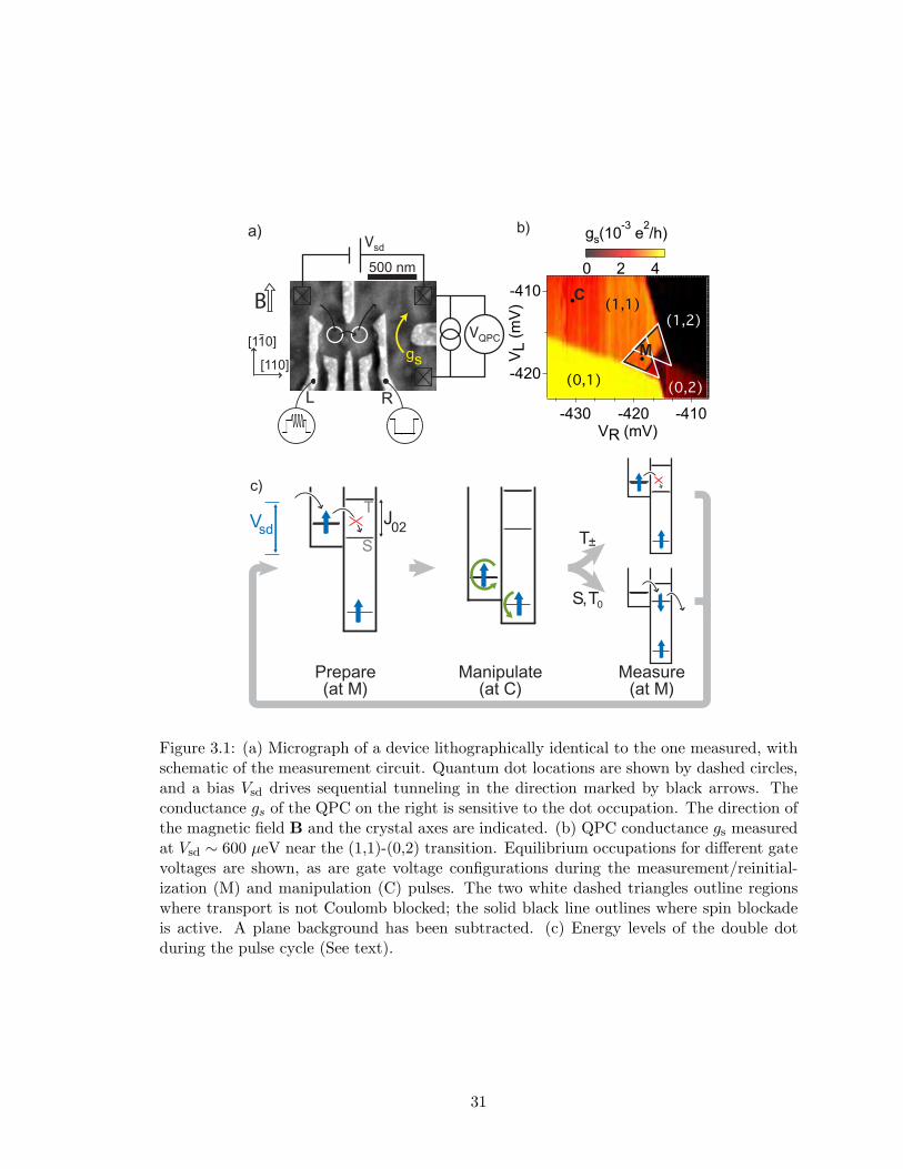
A new mechanism of electric dipole spin resonance 3
500 nm
RL
a) b)
c)
sdV J
02
S
T
S, T0
T±
Prepare(at M)
Manipulate(at C)
Measure(at M)
-420
-410
VL (
mV
)
-430 -420 -410VR (mV)
(1,1)(1,2)
(0,1)(0,2)
0 2 4
gs(10-3
e2/h)
VQPC
Vsd
C
gs
B
M[110]
[110]
Figure 1. (a) Micrograph of a device lithographically identical to the one measured,with schematic of the measurement circuit. Quantum dot locations are shown bydashed circles, and a bias Vsd drives sequential tunneling in the direction markedby black arrows. The conductance gs of the QPC on the right is sensitive to thedot occupation. The direction of the magnetic field B and the crystal axes areindicated. (b) QPC conductance gs measured at Vsd ∼ 600 µeV near the (1,1)-(0,2)transition. Equilibrium occupations for different gate voltages are shown, as are gatevoltage configurations during the measurement/reinitialization (M) and manipulation(C) pulses. The two white dashed triangles outline regions where transport is notCoulomb blocked; the solid black line outlines where spin blockade is active. A planebackground has been subtracted. (c) Energy levels of the double dot during the pulsecycle (See text).
The characteristic feature of tunnel-coupled quantum dots is a discrete electron
energy spectrum. An overall shift to the spectrum, proportional to the electron
occupation, is induced by VL and VR, which therefore determine which occupation is
energetically favoured. Figure 1(b) shows the QPC conductance gs as a function of
VL and VR; different conductances correspond to different (NL, NR). For most VL, VR
configurations, only one value of (NL, NR) is energetically accessible; these correspond
in Figure 1(b) to regions of uniform gs.
A bias Vsd applied across the device drives electron transport via sequential
tunneling subject to two constraints [24]. The first constraint, Coulomb blockade, arises
because for most gate configurations electrostatic repulsion prevents additional electrons
from tunneling onto either dot. This constraint inhibits transport except when VL, VR are
tuned so that three occupation configurations are near-degenerate. The energy cost of an
extra electron tunneling through the device is then small enough to be provided by the
bias voltage. Values of VL and VR satisfying this condition correspond to the two white
Figure 3.1: (a) Micrograph of a device lithographically identical to the one measured, withschematic of the measurement circuit. Quantum dot locations are shown by dashed circles,and a bias Vsd drives sequential tunneling in the direction marked by black arrows. Theconductance gs of the QPC on the right is sensitive to the dot occupation. The direction ofthe magnetic field B and the crystal axes are indicated. (b) QPC conductance gs measuredat Vsd ∼ 600 µeV near the (1,1)-(0,2) transition. Equilibrium occupations for different gatevoltages are shown, as are gate voltage configurations during the measurement/reinitial-ization (M) and manipulation (C) pulses. The two white dashed triangles outline regionswhere transport is not Coulomb blocked; the solid black line outlines where spin blockadeis active. A plane background has been subtracted. (c) Energy levels of the double dotduring the pulse cycle (See text).
31
(0, 2) transition selective in the two-electron spin state, inhibited for triplet states but
allowed for the singlet. The hyperfine field difference between dots converts the ms = 0
component T0 of the blocked triplet T to an unblocked singlet S within ∼ 10 ns, as we have
confirmed by the technique of [Petta 2005]. However, decay of ms = ±1 components T±
requires a spin flip and therefore proceeds much more slowly. This spin flip becomes the
rate-limiting step in transport, and so the time-averaged occupation is dominated by the
(1,1) portion of the transport sequence [Johnson PRB 2005]. Gate configurations where
spin blockade applies correspond to the black solid outlined region of Figure 1(b); inside
this region, gs has the value corresponding to (1,1). Any process that induces spin flips will
partially break spin blockade and lead to a decrease in gs.
Unless stated otherwise, EDSR is detected via changes in gs while the following cycle
of voltage pulses VL and VR [Koppens 2006] is applied to L and R (Figure 1(c)). The cycle
begins inside the spin blockade region (M in Figure 1(b)), so that the two-electron state is
initialized to (1, 1)T± with high probability. A ∼1 µs pulse to point C prevents electron
tunneling regardless of spin state. Towards the end of this pulse, a microwave burst of
duration τEDSR at frequency f is applied to gate L. Finally the system is brought back to M
for ∼3 µs for readout/reinitialization. If and only if a spin (on either dot) was flipped during
the pulse, the transition (1, 1) → (0, 2) occurs, leading to a change in average occupation
and in gs. If this transition occurs, subsequent electron transitions reinitialize the state to
(1, 1)T± by the end of this step, after which the pulse cycle is repeated. This pulsed EDSR
scheme has the advantage of separating spin manipulation from readout.
Changes in gs are monitored via the voltage VQPC across the QPC sensor biased at
5 nA. For increased sensitivity, the microwaves are chopped at 227 Hz and the change in
voltage δVQPC is synchronously detected using a lock-in amplifier. We interpret δVQPC as
proportional to the spin-flip probability during a microwave burst, averaged over the 100 ms
lock-in time constant.
32
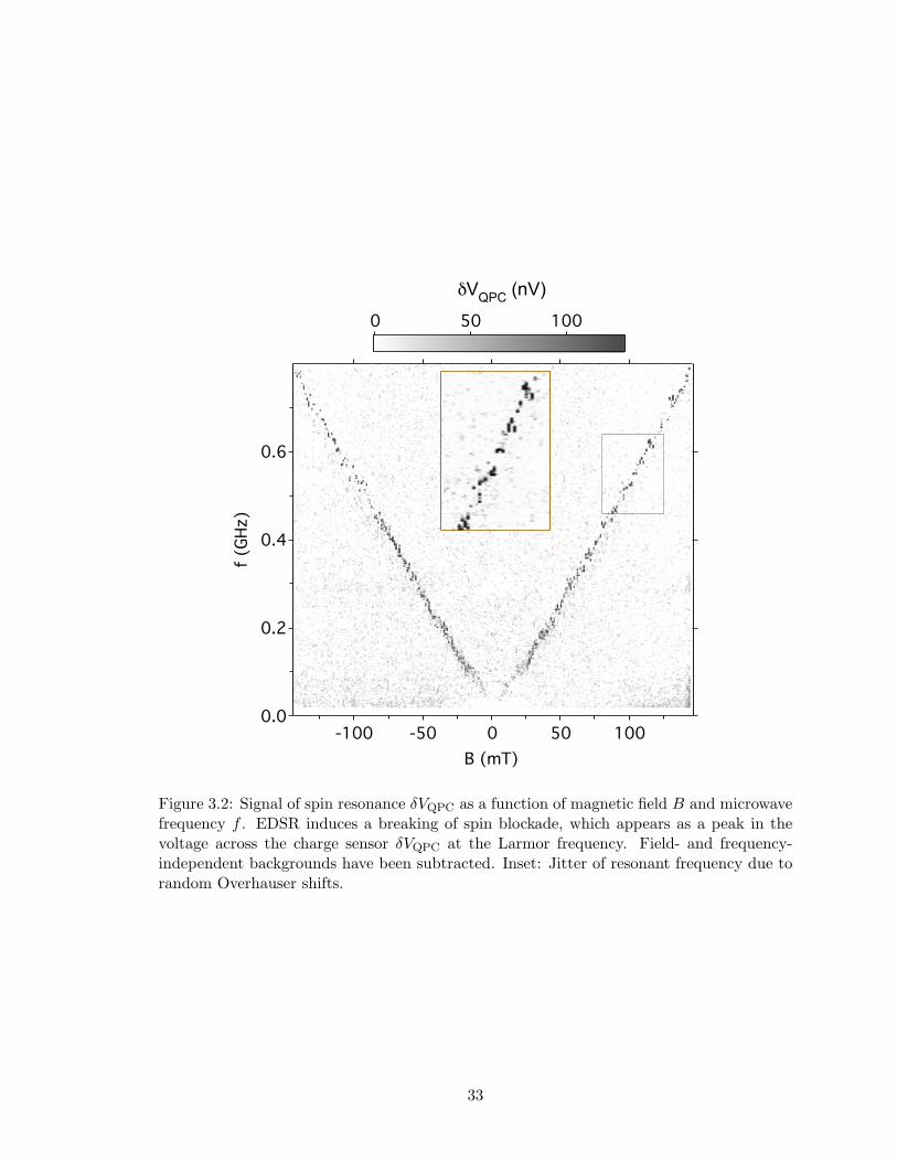
A new mechanism of electric dipole spin resonance 5
0.6
0.4
0.2
0.0
f (G
Hz)
-100 -50 0 50 100
B (mT)
100500
!VQPC
(nV)
Figure 2. Signal of spin resonance δVQPC as a function of magnetic field B and
microwave frequency f . EDSR induces a breaking of spin blockade, which appears
as a peak in the voltage across the charge sensor δVQPC at the Larmor frequency.
Field- and frequency-independent backgrounds have been subtracted. Inset: Jitter of
resonant frequency due to random Overhauser shifts.
(Figure 2 inset) to Overhauser shift caused by the time-varying hyperfine field acting
on the electron spin. Their range is ∼ ±22 MHz, corresponding to a field of ∼ 4 mT,
consistent with Overhauser fields in similar devices [30, 31, 27].
Information about the EDSR mechanism can be obtained by studying the peak
height as a function of duration, strength, and frequency of the microwave burst
(Figure 3). To reduce the effects of the shifting Overhauser field, the microwave source
is frequency modulated at 3 kHz in a sawtooth pattern with depth 36 MHz about a
central frequency f . The resonance line as a function of τEDSR is shown in the inset of
Figure 3(a). For equal microwave power at two different frequencies f , the peak heights
δV peakQPC are plotted in Figure 3(a) (main panel). The two data sets are similar in turn-on
time and saturation value; this is the case for frequencies up to f = 6 GHz. From similar
data (insets of Figure 3(b)), using theory to be described, we extract the dependence of
the spin-flip rate ΩR on microwave power PMW shown in the main panel of Figure 3(b).
Coherent Rabi-type oscillations in δV peakQPC (τEDSR) are not observed for any microwave
power or magnetic field over the range measured.
The B-independence of the EDSR strength rules out spin-orbit mediated EDSR
of the k − σ type (either Dresselhaus or Rashba), for which the Rabi frequency is
proportional to B [4, 13, 14]. This is in contrast to the results of [14], where the spin-
orbit effect was found to dominate in a similar device to ours. A possible explanation
is the device orientation relative to B and the crystal axes. In both our experiment
Figure 3.2: Signal of spin resonance δVQPC as a function of magnetic field B and microwavefrequency f . EDSR induces a breaking of spin blockade, which appears as a peak in thevoltage across the charge sensor δVQPC at the Larmor frequency. Field- and frequency-independent backgrounds have been subtracted. Inset: Jitter of resonant frequency due torandom Overhauser shifts.
33
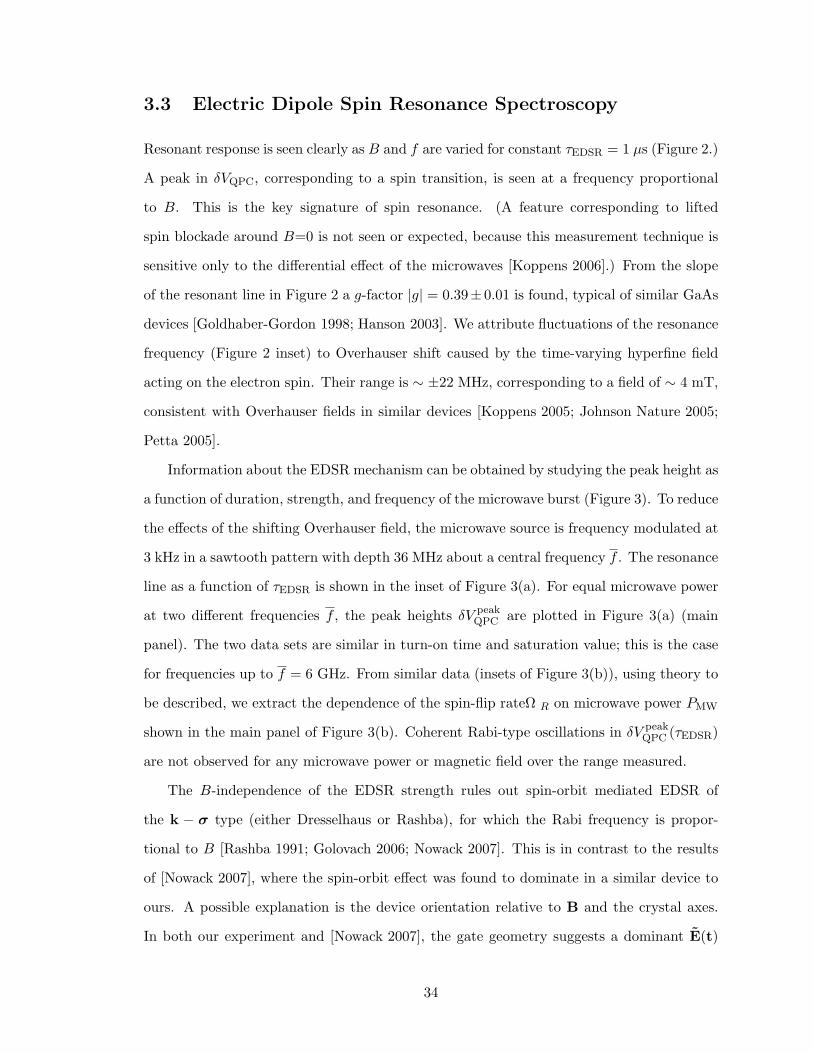
3.3 Electric Dipole Spin Resonance Spectroscopy
Resonant response is seen clearly as B and f are varied for constant τEDSR = 1 µs (Figure 2.)
A peak in δVQPC, corresponding to a spin transition, is seen at a frequency proportional
to B. This is the key signature of spin resonance. (A feature corresponding to lifted
spin blockade around B=0 is not seen or expected, because this measurement technique is
sensitive only to the differential effect of the microwaves [Koppens 2006].) From the slope
of the resonant line in Figure 2 a g-factor |g| = 0.39± 0.01 is found, typical of similar GaAs
devices [Goldhaber-Gordon 1998; Hanson 2003]. We attribute fluctuations of the resonance
frequency (Figure 2 inset) to Overhauser shift caused by the time-varying hyperfine field
acting on the electron spin. Their range is ∼ ±22 MHz, corresponding to a field of ∼ 4 mT,
consistent with Overhauser fields in similar devices [Koppens 2005; Johnson Nature 2005;
Petta 2005].
Information about the EDSR mechanism can be obtained by studying the peak height as
a function of duration, strength, and frequency of the microwave burst (Figure 3). To reduce
the effects of the shifting Overhauser field, the microwave source is frequency modulated at
3 kHz in a sawtooth pattern with depth 36 MHz about a central frequency f . The resonance
line as a function of τEDSR is shown in the inset of Figure 3(a). For equal microwave power
at two different frequencies f , the peak heights δV peakQPC are plotted in Figure 3(a) (main
panel). The two data sets are similar in turn-on time and saturation value; this is the case
for frequencies up to f = 6 GHz. From similar data (insets of Figure 3(b)), using theory to
be described, we extract the dependence of the spin-flip rateΩ R on microwave power PMW
shown in the main panel of Figure 3(b). Coherent Rabi-type oscillations in δV peakQPC (τEDSR)
are not observed for any microwave power or magnetic field over the range measured.
The B-independence of the EDSR strength rules out spin-orbit mediated EDSR of
the k − σ type (either Dresselhaus or Rashba), for which the Rabi frequency is propor-
tional to B [Rashba 1991; Golovach 2006; Nowack 2007]. This is in contrast to the results
of [Nowack 2007], where the spin-orbit effect was found to dominate in a similar device to
ours. A possible explanation is the device orientation relative to B and the crystal axes.
In both our experiment and [Nowack 2007], the gate geometry suggests a dominant E(t)
34
A new mechanism of electric dipole spin resonance 6
100
80
60
40
20
0
!V
peak(n
V)
0.80.60.40.20.0"
EDSR (µs)
0.17 GHz, 44 mT 2.9 GHz, 550 mT
50
40
0.80.60.40.20.0"
EDSR (µs)
0.17 GHz
560
550
2.9 GHz 60
40
20
0
5
6
7
8
9
1
#R
(10
6s
-1)
9
0.12 3 4 5 6 7 8 9
1PMW (mW)
0.91 GHz185 mT
30
20
10
0!V
pe
ak (
nV
)
10"EDSR (µs)
30
20
10
0!V
pe
ak (
nV
)
210"EDSR (µs)
!VQPC
(nV)
a)
b)
B (
mT
)
QP
C
QP
C
QP
C
Figure 3. (a) Measured EDSR peak strength δV peakQPC (symbols) versus microwave
pulse duration τEDSR for two frequencies, along with theoretical fits (curves) obtainedby numerically evaluating and scaling Equation (4) (see text). Both the applied power(PMW ∼ 0.6 mW) and the calibrated power at the device are equal at these twofrequencies (see footnote to Section 4.1). Inset: Raw data from which the points inthe main figure are extracted. Each vertical cut corresponds to one point in the mainfigure. Jitter in the field position of the resonance reflects time-dependent Overhausershifts. (b) Spin-flip rate ΩR as a function of applied microwave power PMW, alongwith a fit to the form ΩR ∝
√PMW (dashed line). Insets: δV peak
QPC versus τEDSR for twovalues of the microwave power, showing the fits from which points in the main figureare derived.
and [14], the gate geometry suggests a dominant E(t) oriented along one of the diagonal
axes ([110] or [110]), leading to an in-plane spin-orbit effective field BSOeff perpendicular
to E(t). In our geometry (see Figure 1(a)), this orientation of BSOeff is parallel to B,
and therefore ineffective at driving spin transitions. In the geometry of [14], B is
perpendicular to BSOeff , so that the k− σ spin-orbit mechanism becomes more efficient.
Although the strength of the EDSR line is field-independent, the hyperfine-induced
jitter becomes more pronounced with increasing field. As seen from the upper inset to
Figure 3(a), repeated scans over the resonance at high field display larger fluctuations
in the position of the peak center. This difference presumably reflects slower nuclear
spin diffusion [32] as well as incipient polarization (see Section 5). In none of the data
was any periodicity of the jitter detectible [33].
Figure 3.3: (a) Measured EDSR peak strength δV peakQPC (symbols) versus microwave pulse du-
ration τEDSR for two frequencies, along with theoretical fits (curves) obtained by numericallyevaluating and scaling Equation (4) (see text). Both the applied power (PMW ∼ 0.6 mW)and the calibrated power at the device are equal at these two frequencies (see footnote toSection 4.1). Inset: Raw data from which the points in the main figure are extracted. Eachvertical cut corresponds to one point in the main figure. Jitter in the field position of theresonance reflects time-dependent Overhauser shifts. (b) Spin-flip rateΩ R as a function ofapplied microwave power PMW, along with a fit to the formΩ R ∝
√PMW (dashed line).
Insets: δV peakQPC versus τEDSR for two values of the microwave power, showing the fits from
which points in the main figure are derived.
35
oriented along one of the diagonal axes ([110] or [110]), leading to an in-plane spin-orbit
effective field BSOeff perpendicular to E(t). In our geometry (see Figure 1(a)), this orientation
of BSOeff is parallel to B, and therefore ineffective at driving spin transitions. In the geome-
try of [Nowack 2007], B is perpendicular to BSOeff , so that the k − σ spin-orbit mechanism
becomes more efficient.
Although the strength of the EDSR line is field-independent, the hyperfine-induced
jitter becomes more pronounced with increasing field. As seen from the upper inset to
Figure 3(a), repeated scans over the resonance at high field display larger fluctuations in
the position of the peak center. This difference presumably reflects slower nuclear spin
diffusion [Reilly 2007] as well as incipient polarization (see Section 5). In none of the data
was any periodicity of the jitter detectible [Ono 2004].
3.4 Theory
A theoretical description of δV peakQPC (τEDSR) and its dependence on B and PMW can be
obtained by modeling EDSR as arising from the coupling of an electron in a single dot to
an oscillating electric field E(t) and the hyperfine field of an ensemble of nuclei 2 [Laird 2007;
Rashba 2008]. Then the center of the dot oscillates as R(t) = −eE(t)/mω20, where m is
the electron effective mass, and ω0 is its confinement frequency in a parabolic dot. As
a result, the Hamiltonian of the hyperfine coupling of the electron spin S = σ/2 with
spatial coordinate r to nuclear spins Ij located at rj becomes time dependent, Hhf =
AΣjδ(r + R(t)− rj)(Ij · S). Here A is the hyperfine coupling constant and the summation
over j runs over all nuclear spins. After expanding Hhf in R(t) (assumed small compared to
the dot size) and averaging over the orbital ground-state wave function ψ0(r) of the dot, the
time dependent part of Hhf becomes Hhf(t) = J(t) · σ, where J(t) is an operator in all Ij .
Choosing the z-axis in spin space along B, the components of J(t) are Jz = 12A
j ψ2
0(rj)Izj
and
2There exists some physical similarity between the hyperfine mechanism of EDSR described in this chapterand EDSR due to the coupling of electron spin to a random exchange field in semimagnetic semiconduc-tors [Khazan 1993].
36
J±(t) =eA
mω20
j
ψ0(rj)E(t) ·∇ψ0(rj)I±j . (3.1)
The time-dependent off-diagonal components J±(t) drive EDSR, while the quasi-static
diagonal component Jz describes detuning of EDSR from the Larmor frequency ωL by an
amount ωz randomly distributed as ρ(ωz) = exp(−ω2z/∆2)/(∆
√π) [Merkulov 2002]. The
dispersions ∆ of the detuning andΩ R of the Rabi frequency are the root-mean-square values
of Jz and J± respectively. Whereas Jz is dominated by fluctuations of Ij symmetric about
the dot centre, J± is dominated by fluctuations antisymmetric in the E direction because
E ·∇ψ0(r) is odd with respect to the E projection of r. Finally,
∆ =A
2
I(I + 1)mω0n0
2πd, ΩR =
eEA
2ω0
I(I + 1)n0
8πd, (3.2)
with I = 3/2 for GaAs, n0 the nuclear concentration, and d the vertical confinement. It is
seen thatΩ R is independent of B; this is in contrast to EDSR mediated by the conventional
k−σ spin-orbit coupling, where Kramers’ theorem requires that the Rabi frequency vanish
linearly as B → 0 [Rashba 1991; Levitov 2003; Golovach 2006].
In an instantaneous nuclear spin configuration with detuning δω = 2πf − (ωL +ωz) and
Rabi frequency Ω, the spin-flip probability from an initial ↑ spin state is [Rabi 1937]:
p↓(τEDSR) =Ω2
(δω/2)2 + Ω2sin2
(δω/2)2 + Ω2 τEDSR
. (3.3)
(We neglect the electron spin relaxation and nuclear-spin dynamics, which remain slow
compared with the Rabi frequency even in the EDSR regime [Petta 2005; Rashba 2008].)
To compare with the time-averaged data of Figure 3, we average Equation (3.3) over ωz
with weight ρ(ωz) and over Ω with weight ρ(Ω) = 2Ω exp(−Ω2/Ω2R)/Ω2
R. This latter distri-
bution arises because the J± acquire Gaussian-distributed contributions from both Ixj and
Iyj components of the nuclear spins, hence it is two-dimensional. Averaging over ωz and
Ω results in a mean-field theory of the hyperfine-mediated EDSR. The resulting spin-flip
37
probability
p↓(τEDSR; ∆,ΩR) = +∞
−∞dωz ρ(ωz)
+∞
0dΩ ρ(Ω)p↓(τEDSR) (3.4)
shows only a remnant of Rabi oscillations as a weak overshoot at τEDSR ∼ Ω−1R . The ab-
sence of Rabi oscillations is characteristic of hyperfine-driven EDSR when the measurement
integration time exceeds the nuclear evolution time [Reilly 2007], and arises because J±
average to zero.
3.4.1 Comparison with Data
To compare theory and experiment, the probability p↓(τEDSR; ∆,ΩR) is scaled by a QPC
sensitivity V 0QPC to convert to a voltage δV peak
QPC . After scaling, numerical evaluation of
Equation (4) gives the theoretical curves shown in Figure 3(a). The parameters that de-
termine these curves are as follows: The Larmor frequency spread, ∆ = 2π × 28 MHz, is
taken as the quadrature sum of the jitter amplitude seen in Figure 2 and half the frequency
modulation depth, whereasΩ R and V 0QPC are numerical fit parameters. The 44 mT data
(green curve in Figure 3(a)) giveΩ R = 1.7× 10⁶ s−1 and V 0QPC = 2.4 µV. Holding V 0
QPC to
this value, the 550 mT data giveΩ R = 1.8 × 10⁶ s−1 (blue curve in Figure 3(a)) and the
185 mT data give the dependence ofΩ R on microwave power PMW shown in Figure 3(b).
The Rabi frequencyΩ R increases as√
PMW (Figure 3(b)) and is independent of B, both
consistent with Equation (1). The B-independence ofΩ R — also evident in the EDSR
intensity in Figure 2—and the absence of Rabi oscillations support our interpretation of
hyperfine-mediated EDSR in the parameter range investigated 3
Estimating ω0 ∼ 1 meV [Hanson 2003], E ∼ 3 × 10³ Vm−1 at maximum applied
power 4, d ∼ 5 nm, and using values from the literature n0 = 4×1028 m−3 and An0=90 µeV
3AlthoughΩ R is found to be substantially smaller than the inhomogeneous dephasing rate 1/T ∗2 ∼100 MHz, oscillations would still be expected from a coherent process. Quasistatic dephasing processes, suchas the hyperfine process dominant here, allow Rabi oscillations to persist even whenΩ T ∗2 is considerablyless than unity [Nowack 2007; Koppens 2007].
4The power at the device is calibrated separately at each frequency from the threshold for non-resonantlifting of spin blockade, which we take to indicate a microwave amplitude large enough to configure the dot
38
[Paget 1977] we calculateΩ R ∼ 11× 106 s−1, an order of magnitude larger than measured.
The discrepancy may reflect uncertainty in our estimate of E.
We have neglected any effect of residual exchange in (1,1) during the ESR burst.
From the width of the (1,1)-(0,2) charge transition, the interdot tunnel rate tc is de-
duced to be much smaller than Boltzmann’s constant multiplied by the electron temper-
ature [Dicarlo 2004]. From the known (1,1)-(0,2) energy detuning with gate voltages
configured at C, we estimate an upper bound on the (1,1) exchange t2c/ 80 neV, of the
same order as the hyperfine coupling. Since different choices of point C give qualitatively
similar results, we conclude that (1,1) exchange is negligible.
Above, we generalized a mean-field description of the hyperfine interaction [Khaetski 2002;
Merkulov 2002] to the resonance regime. Justification for this procedure was provided re-
cently in [Rashba 2008]. A distinctive feature of the mean-field theory is a weak overshoot,
about 10 - 15%, that is expected in the data of Fig. 3(a) before δV peakQPC (τEDSR) reaches
its asymptotic value at τEDSR → ∞. No overshoot is observed in the 550 mT data (blue
symbols in Figure 3(a)), which was taken in a parameter range where an instability of the
nuclear polarization begins to develop; see Section 5. For the 44 mT data (green symbols
in Figure 3(a)), a considerable spread of experimental points does not allow a specific con-
clusion regarding the presence or absence of an overshoot. The theory of [Rashba 2008]
suggests that the existence of the overshoot is a quite general property of the mean-field
theory. However, after passing the maximum, the signal decays to its saturation value vary
fast, with Gaussian exponent e−Ω2Rτ2
EDSR . By contrast, the first correction to the mean-field
theory decays slowly, as 1/(NΩ2Rτ2
EDSR), where N is the number of nuclei in the dot. As
a result, the two terms become comparable at τEDSR ∼√
lnN/ΩR, which should make
the maximum less pronounced. Because for N ∼ 105 the factor√
lnN ∼ 3, the correc-
tions to the mean-field theory manifest themselves surprisingly early, at times only about
τEDSR ≈ 3/ΩR, making the overshoot difficult to observe.
temporarily in a different charge state. This amplitude corresponds in Figure 1(b) to the 4mV distance frompoint C to the nearest charge transition. The data in Figure 3(a) and the last data point in Figure 3(b) usepower 2± 1 dB below this threshold, corresponding to 3.2 mV. Dropped uniformly across the 500 nm widthof the device this voltage gives a field E ∼ 3× 10³ Vm−1.
39
3.5 Nuclear Polarization
Consistent with a hyperfine mechanism, this EDSR effect can create a non-equilibrium
nuclear polarization [Baugh 2007]. If f is scanned repeatedly over the resonance at high
power, a shift of the resonance develops (Figure 4(a)), corresponding to a nuclear spin
alignment parallel to B. The effect is stronger at higher B, and saturates over a timescale
∼ 200 s. In Figure 4(b), we show how to build up a substantial polarization: While slowly
increasing B, we scan f repeatedly downwards, i. e., in the direction which tracks the mov-
ing resonance. The resonance frequency remains approximately fixed, showing that the
developing polarization compensates the increase in B. From the maximum line displace-
ment from equilibrium, an effective hyperfine field of 840 mT can be read off, corresponding
to a nuclear polarization of ∼ 16%. Figure 4(c) shows similar data for lower power and
opposite frequency sweep direction, indicating the approximate equilibrium line position.
Figure 4(d), similar to Figure 4(b) but with a faster sweep rate, makes the displacement
and eventual escape of the resonance clearer although the maximum polarization is less.
The resonance shift is observed to be towards lower frequency, corresponding to a nu-
clear polarization parallel to B. This can be understood if the pulse cycle preferentially
prepares the electron ground state T+ over T−, either because it is more efficiently loaded
or because of electron spin relaxation. EDSR then transfers this electron polarization to
the nuclei [Rudner 2007]. We emphasize that the line shift is opposite to what is given
by the usual Overhauser mechanism for inducing nuclear polarization via electron reso-
nance [Overhauser 1953; Gueron 1959].
3.6 Addressing individual Spins
In quantum information applications, it is desirable to address individual spins selec-
tively [Loss 1998]. A scheme to allow this is presented in Figure 5. In an otherwise similar
device (Figure 5(a)), we incorporated a 100 nm thick micron-scale permalloy (84% Ni, 16%
Fe) magnet over 35 nm of atomic-layer-deposited alumina [Tokura 2006; Pioro-Ladriere 2007].
This device was measured with external field B normal to the heterostructure plane. A
finite-element simulation of the field Bmag due to the micromagnet, assuming complete
40
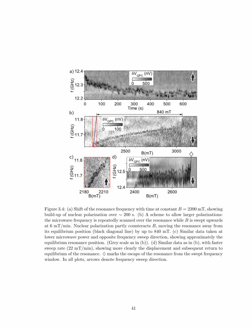
A new mechanism of electric dipole spin resonance 10
Figure 4. (a) Shift of the resonance frequency with time at constant B = 2390 mT,showing build-up of nuclear polarization over ∼ 200 s. (b) A scheme to allow largerpolarizations: the microwave frequency is repeatedly scanned over the resonancewhile B is swept upwards at 6 mT/min. Nuclear polarization partly counteracts B,moving the resonance away from its equilibrium position (black diagonal line) by up to840 mT. (c) Similar data taken at lower microwave power and opposite frequency sweepdirection, showing approximately the equilibrium resonance position. (Grey scale asin (b)). (d) Similar data as in (b), with faster sweep rate (22 mT/min), showingmore clearly the displacement and subsequent return to equilibrium of the resonance.♦ marks the escape of the resonance from the swept frequency window. In all plots,arrows denote frequency sweep direction.
efficiently loaded or because of electron spin relaxation. EDSR then transfers this
electron polarization to the nuclei [21]. We emphasize that the line shift is opposite
to what is given by the usual Overhauser mechanism for inducing nuclear polarization
via electron resonance [43, 18].
6. Addressing individual spins
In quantum information applications, it is desirable to address individual spins
selectively [5]. A scheme to allow this is presented in Figure 5. In an otherwise similar
device (Figure 5(a)), we incorporated a 100 nm thick micron-scale permalloy (84% Ni,
16% Fe) magnet over 35 nm of atomic-layer-deposited alumina [12, 44]. This device was
measured with external field B normal to the heterostructure plane. A finite-element
simulation of the field Bmag due to the micromagnet, assuming complete permalloy
magnetization along B, yields the field profiles shown in Figure 5(b). The difference
in total field Btot = |B + Bmag| between dots is ∼ 5 mT. As expected, the EDSR line
measured in this device is frequently split (Figure 5(c)). The splitting, 10 − 20 mT
Figure 3.4: (a) Shift of the resonance frequency with time at constant B = 2390 mT, showingbuild-up of nuclear polarization over ∼ 200 s. (b) A scheme to allow larger polarizations:the microwave frequency is repeatedly scanned over the resonance while B is swept upwardsat 6 mT/min. Nuclear polarization partly counteracts B, moving the resonance away fromits equilibrium position (black diagonal line) by up to 840 mT. (c) Similar data taken atlower microwave power and opposite frequency sweep direction, showing approximately theequilibrium resonance position. (Grey scale as in (b)). (d) Similar data as in (b), with fastersweep rate (22 mT/min), showing more clearly the displacement and subsequent return toequilibrium of the resonance. ♦ marks the escape of the resonance from the swept frequencywindow. In all plots, arrows denote frequency sweep direction.
41
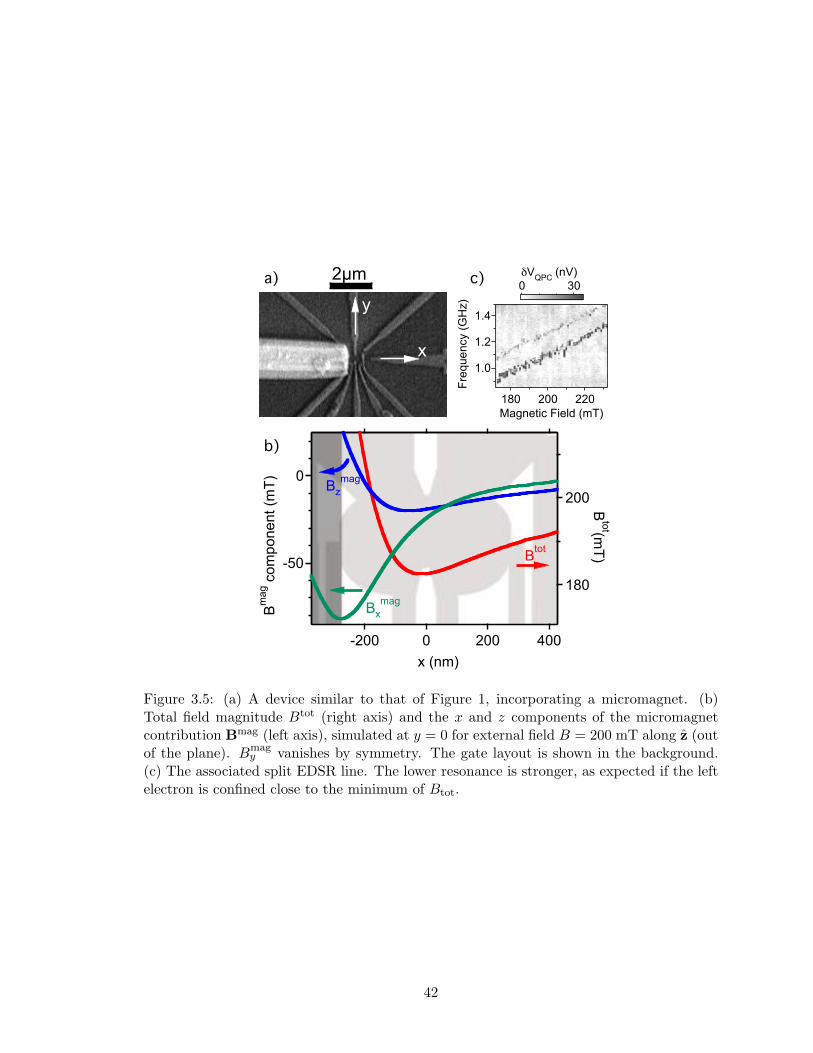
A new mechanism of electric dipole spin resonance 11
2!m
x
y1.4
1.2
1.0
Fre
quency (
GH
z)
220200180
Magnetic Field (mT)
300
!VQPC
(nV)
200
180
Bto
t(mT
)
4002000-200
x (nm)
-50
0
Bm
ag c
om
po
ne
nt
(mT
)
Bz
mag
Bx
mag
Btot
a) c)
b)
Figure 5. (a) A device similar to that of Figure 1, incorporating a micromagnet. (b)Total field magnitude Btot (right axis) and the x and z components of the micromagnetcontribution Bmag (left axis), simulated at y = 0 for external field B = 200 mT along z(out of the plane). Bmag
y vanishes by symmetry. The gate layout is shown in thebackground. (c) The associated split EDSR line. The lower resonance is stronger, asexpected if the left electron is confined close to the minimum of Btot.
depending on precise gate voltage and pulse parameters, is not observed without the
magnet and presumably reflects the field difference between dots. Since this splitting is
considerably larger than the Overhauser field fluctuations, spins in left and right dots
can be separately addressed by matching f to the local resonance condition [15].
The observation of a field difference between dots raises the possibility of EDSR
driven by a field gradient [15]. We cannot exclude a contribution from this effect to the
signal in Figure 5(c); however we did not observe the Rabi oscillations which would be
expected if the field gradient were the primary EDSR mechanism.
7. Open issues and discussion
Finally, we discuss unexplained behavior observed only in the device of Figure 5(a). For
the data described in this section, a simplified measurement scheme is used: Rather
than applying gate pulses, the device is configured in the spin blockade region (point M
in Figure 1(a)) throughout. Microwaves are applied continuously, and spin resonance is
detected by directly measuring the QPC conductance gs.
As well as the EDSR signal at full frequency f = gµBB/h, an unexpected half-
Figure 3.5: (a) A device similar to that of Figure 1, incorporating a micromagnet. (b)Total field magnitude Btot (right axis) and the x and z components of the micromagnetcontribution Bmag (left axis), simulated at y = 0 for external field B = 200 mT along z (outof the plane). Bmag
y vanishes by symmetry. The gate layout is shown in the background.(c) The associated split EDSR line. The lower resonance is stronger, as expected if the leftelectron is confined close to the minimum of Btot.
42
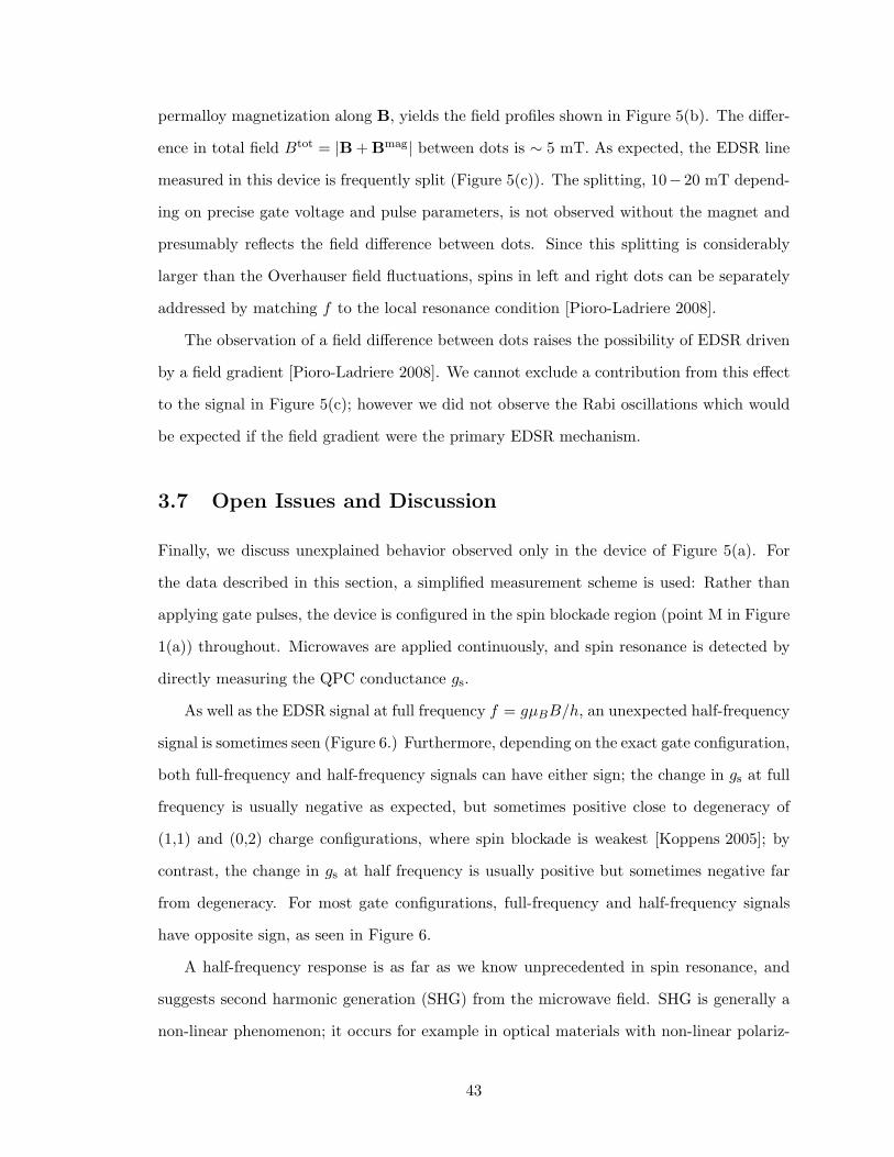
permalloy magnetization along B, yields the field profiles shown in Figure 5(b). The differ-
ence in total field Btot = |B + Bmag| between dots is ∼ 5 mT. As expected, the EDSR line
measured in this device is frequently split (Figure 5(c)). The splitting, 10− 20 mT depend-
ing on precise gate voltage and pulse parameters, is not observed without the magnet and
presumably reflects the field difference between dots. Since this splitting is considerably
larger than the Overhauser field fluctuations, spins in left and right dots can be separately
addressed by matching f to the local resonance condition [Pioro-Ladriere 2008].
The observation of a field difference between dots raises the possibility of EDSR driven
by a field gradient [Pioro-Ladriere 2008]. We cannot exclude a contribution from this effect
to the signal in Figure 5(c); however we did not observe the Rabi oscillations which would
be expected if the field gradient were the primary EDSR mechanism.
3.7 Open Issues and Discussion
Finally, we discuss unexplained behavior observed only in the device of Figure 5(a). For
the data described in this section, a simplified measurement scheme is used: Rather than
applying gate pulses, the device is configured in the spin blockade region (point M in Figure
1(a)) throughout. Microwaves are applied continuously, and spin resonance is detected by
directly measuring the QPC conductance gs.
As well as the EDSR signal at full frequency f = gµBB/h, an unexpected half-frequency
signal is sometimes seen (Figure 6.) Furthermore, depending on the exact gate configuration,
both full-frequency and half-frequency signals can have either sign; the change in gs at full
frequency is usually negative as expected, but sometimes positive close to degeneracy of
(1,1) and (0,2) charge configurations, where spin blockade is weakest [Koppens 2005]; by
contrast, the change in gs at half frequency is usually positive but sometimes negative far
from degeneracy. For most gate configurations, full-frequency and half-frequency signals
have opposite sign, as seen in Figure 6.
A half-frequency response is as far as we know unprecedented in spin resonance, and
suggests second harmonic generation (SHG) from the microwave field. SHG is generally a
non-linear phenomenon; it occurs for example in optical materials with non-linear polariz-
43
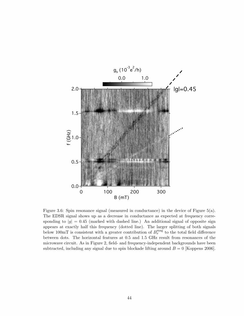
A new mechanism of electric dipole spin resonance 12
!"#
$"%
$"#
#"%
#"#
&'()
*+,
-##!##$###.'(/0,
$"##"#
12'($#3-4!56,
7178#"9%
Figure 6. Spin resonance signal (measured in conductance) in the device of Figure5(a). The EDSR signal shows up as a decrease in conductance as expected at frequencycorresponding to |g| = 0.45 (marked with dashed line.) An additional signal of oppositesign appears at exactly half this frequency (dotted line). The larger splitting of bothsignals below 100mT is consistent with a greater contribution of Bmag
x to the totalfield difference between dots. The horizontal features at 0.5 and 1.5 GHz result fromresonances of the microwave circuit. As in Figure 2, field- and frequency-independentbackgrounds have been subtracted, including any signal due to spin blockade liftingaround B = 0 [9].
frequency signal is sometimes seen (Figure 6.) Furthermore, depending on the exact gate
configuration, both full-frequency and half-frequency signals can have either sign; the
change in gs at full frequency is usually negative as expected, but sometimes positive
close to degeneracy of (1,1) and (0,2) charge configurations, where spin blockade is
weakest [30]; by contrast, the change in gs at half frequency is usually positive but
sometimes negative far from degeneracy. For most gate configurations, full-frequency
and half-frequency signals have opposite sign, as seen in Figure 6.
A half-frequency response is as far as we know unprecedented in spin resonance, and
suggests second harmonic generation (SHG) from the microwave field. SHG is generally
a non-linear phenomenon; it occurs for example in optical materials with non-linear
polarizability [45] and in non-linear electronic components. For hydrogenic donors in a
semiconductor, the nonlinear dependence of g-tensor on electric field has been predicted
to drive EDSR at subharmonics of the Larmor frequency [46]. In our system, a hyperfine
field at a harmonic of the microwave frequency arises if the confinement potential is non-
parabolic.
However, SHG alone does not explain the sign of the conductance change seen
at half-frequency in Figure 6. The positive signal would be consistent with a reduced
Figure 3.6: Spin resonance signal (measured in conductance) in the device of Figure 5(a).The EDSR signal shows up as a decrease in conductance as expected at frequency corre-sponding to |g| = 0.45 (marked with dashed line.) An additional signal of opposite signappears at exactly half this frequency (dotted line). The larger splitting of both signalsbelow 100mT is consistent with a greater contribution of Bmag
x to the total field differencebetween dots. The horizontal features at 0.5 and 1.5 GHz result from resonances of themicrowave circuit. As in Figure 2, field- and frequency-independent backgrounds have beensubtracted, including any signal due to spin blockade lifting around B = 0 [Koppens 2006].
44
ability [Franken 1961] and in non-linear electronic components. For hydrogenic donors in
a semiconductor, the nonlinear dependence of g-tensor on electric field has been predicted
to drive EDSR at subharmonics of the Larmor frequency [De 2009]. In our system, a hy-
perfine field at a harmonic of the microwave frequency arises if the confinement potential is
non-parabolic.
However, SHG alone does not explain the sign of the conductance change seen at half-
frequency in Figure 6. The positive signal would be consistent with a reduced admixture
of (0,2), corresponding to a unexpected enhancement of the spin lifetime by microwaves.
Alternatively, a positive signal could be caused by an admixture of the (0,1) charge state;
but it is observed even for the gate configurations where (0,1) is energetically inaccessible
(in the top right of the spin blockade region of Figure 1(b)). Also, there is no reason why
(0,1) should be admixed for one resonance but not the other. These anomalous behaviours
are therefore left unexplained.
Acknowledgements
We acknowledge useful discussions with Al. L. Efros, H.-A. Engel, F. H. L. Koppens, J. R.
Petta, D. J. Reilly, M. S. Rudner, J. M. Taylor, and L. M. K. Vandersypen. We acknowledge
support from the DTO and from DARPA. E. I. R. was supported in part by a Rutherford
Professorship at Loughborough University, U.K.
45
Chapter 4
Rapid Single-Shot Measurement ofa Singlet-Triplet Qubit
C. Barthel1 D. J. Reilly1,2 C. M. Marcus1 M. P. Hanson3 A. C. Gossard3
1Department of Physics, Harvard University, 17 Oxford Street, Cambridge, Massachusetts
02138, USA
2School of Physics, University of Sydney, Sydney, 2006, Australia
3Materials Department, University of California, Santa Barbara, California 93106, USA
We report repeated single-shot measurements of the two-electron spin state in a GaAs
double quantum dot. The readout scheme allows measurement with fidelity above 90% with
a ∼ 7 µs cycle time. Hyperfine-induced precession between singlet and triplet states of the
two-electron system are directly observed, as nuclear Overhauser fields are quasi-static on
the time scale of the measurement cycle. Repeated measurements on millisecond to second
time scales reveal evolution of the nuclear environment 1.
1This chapter is adapted from Ref. [Barthel 2009] with permission, c(2009) by the American PhysicalSociety
46
4.1 Introduction
Qubits constructed from spin states of confined electrons are of interest for quantum infor-
mation processing [Loss 1998], for investigating decoherence and controlled entanglement,
and as probes of mesoscopic nuclear spin environments. For logical qubits formed from pairs
of electron spins in quantum dots [Levy 2002], several requirements for quantum comput-
ing [DiVincenzo 1998] have been realized [Petta 2005; Nowack 2007; Pioro-Ladriere 2008;
Reilly 2008]. To date, however, measurements of these systems have constituted ensem-
ble averages over time, while protocols for quantum control, including quantum error
correction, typically require high-fidelity single-shot readout. Coherent evolution con-
ditional on individual measurement outcomes can give rise to interesting non-classical
states [Armen 2002; Romito 2008]. Rapidly repeated single-shot measurements can also
give access to the dynamics of the environment, allowing, for instance, feedback-controlled
manipulation of the nuclear state. Single-shot measurements of solid-state quantum systems
have been reported for superconducting qubits [Astafiev 2004], the charge state of a single
quantum dot [Lu 2003], the spin of a single electron in a quantum dot in large magnetic
fields [Elzerman 2004; Amasha 2008], and the two-electron spin state in a single quantum
dot [Meunier 2006].
In this chapter, we demonstrate rapidly repeated high-fidelity single-shot measurements
of a two-electron spin (singlet-triplet) qubit in a double quantum dot. Singlet and triplet
spin states are mapped to charge states [Petta 2005], which are measured by a radio-
frequency quantum point contact (rf-QPC) that is energized only during readout. The
measurement integration time required for > 90% readout fidelity is a few microseconds.
On that time scale, nuclear Overhauser fields are quasi-static, leading to observed peri-
odic precession of the qubit. By measuring over longer times, the evolution of the Over-
hauser fields from milliseconds to several seconds can be seen as well. We apply a model
of single-shot readout statistics that accounts for T1 relaxation, and find good agreement
with experiment. Finally, we examine the evolution of the two-electron spin state at the
resonance between the singlet (S) and the m = +1 triplet (T+) via repeated single-shot
measurement, and show that the transverse component of the Overhauser field difference is
47
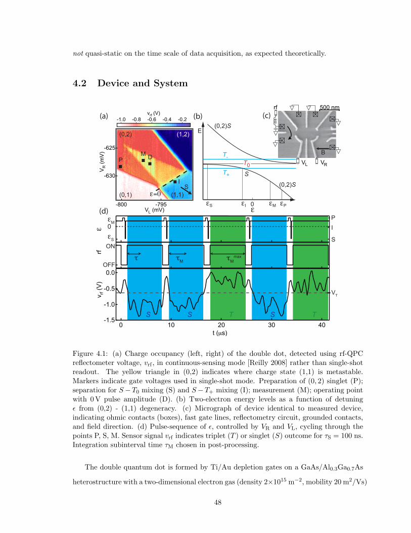
not quasi-static on the time scale of data acquisition, as expected theoretically.
4.2 Device and System
M M
max
VT
S
I
P
ON
OFF
M
S
0
S S T TS
0
E(0,2)S
(0,2)S
T-
T+
S I M P
T0
S
(b)
V VL R
500 nmrf
(c)
(1,2)
(1,1)(0,1)
(0,2)
MD
P
SI
B
(d)
(a)
Figure 4.1: (a) Charge occupancy (left, right) of the double dot, detected using rf-QPCreflectometer voltage, vrf , in continuous-sensing mode [Reilly 2008] rather than single-shotreadout. The yellow triangle in (0,2) indicates where charge state (1,1) is metastable.Markers indicate gate voltages used in single-shot mode. Preparation of (0, 2) singlet (P);separation for S−T0 mixing (S) and S−T+ mixing (I); measurement (M); operating pointwith 0 V pulse amplitude (D). (b) Two-electron energy levels as a function of detuning from (0,2) - (1,1) degeneracy. (c) Micrograph of device identical to measured device,indicating ohmic contacts (boxes), fast gate lines, reflectometry circuit, grounded contacts,and field direction. (d) Pulse-sequence of , controlled by VR and VL, cycling through thepoints P, S, M. Sensor signal vrf indicates triplet (T ) or singlet (S) outcome for τS = 100 ns.Integration subinterval time τM chosen in post-processing.
The double quantum dot is formed by Ti/Au depletion gates on a GaAs/Al0.3Ga0.7As
heterostructure with a two-dimensional electron gas (density 2×10¹⁵ m−2, mobility 20 m2/Vs)
48
100 nm below the surface. In order to split the three triplets, an in-plane magnetic field,
B, larger than the typical Overhauser fields is applied along the line between dot centers.
Except where noted, B = 200 mT. As described elsewhere [Reilly APL 2007], a proximal
radio-frequency quantum point contact (rf-QPC) is sensitive to the charge state of the
double dot, yielding an output signal vrf via reflectometry, with sub-microsecond time reso-
lution. The charge state of the double dot is controlled by fast-pulsed gate voltages VL and
VR from two synchronized Tektronix AWG710B arbitrary waveform generators.
Energy levels of the system as a function of detuning, , from the (1,1) - (0,2) charge
degeneracy (controlled by VR and VL) are shown in Fig. 5.1(b). The qubit comprises the
two-electron singlet (S) and m = 0 triplet (T0) of the (1,1) charge state [Petta 2005]. A
pulse cycle [Fig. 5.1(d)] first prepares a spin singlet in (0, 2) by waiting at point P (near
the edge of (0,2)) for τP = 400 ns, then moving to a separation point S (I), where S and
T0 (S and T+) are nearly degenerate, for a time τS (τI). Finally the system is brought
to the measurement point M for a time τmaxM . If the separated electrons are in a singlet
configuration when the system is pulsed to M, the system will return to (0, 2), which will
be detected by the rf-QPC. If the two electrons are in a triplet state, they will remain in
(1, 1) at point M, and detected accordingly. Coherent superpositions will be projected to
the corresponding charge state during measurement. The rf-QPC is only energized during
read-out, at point M [Fig. 5.1(d)].
4.3 Single-shot Measurement and Fidelity
The rf-QPC conductance is ∼ 5% higher in (0,2) than in (1,1), yielding a charge sensitivity
of 6 × 10⁻⁴ e/Hz−1/2, i.e., unity signal-to-noise after 400 ns of integration. To increase
fidelity, single-shot outcomes are averaged over a sub-interval τM of the full measurement
time τmaxM , Vrf = 1/τM
τM0 vrf(τ)dτ . By designating a threshold voltage VT, outcomes can
be classified as singlet for Vrf < VT or triplet otherwise. Optimization of τM and VT is
described below.
Figure 4.2(a) shows 7000 consecutive one-shot measurements of the S − T0 qubit with
τS ranging from 1 – 200 ns, stepped by ∼ 6 ns every 200 cycles. For these data, the in-
49
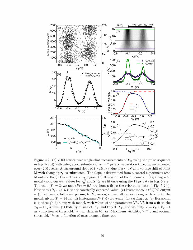
VrfT
VrfS
(a)
(b)
(g)
(d)
(e)
(f)
(c)
S T
Figure 4.2: (a) 7000 consecutive single-shot measurements of Vrf using the pulse sequencein Fig. 5.1(d) with integration subinterval τM = 7 µs and separation time, τS, incrementedevery 200 cycles. A background slope of Vrf with τS, due to a ∼ µV gate voltage shift of pointM with changing τS, is subtracted. The slope is determined from a control experiment withM outside the (1,1) - metastability region. (b) Histogram of the outcomes in (a), along withmodel (solid curve). Values for V S
rf and∆ Vrf are fit once using the 15 µs data in Fig. 5.2(e).The value T1 = 34 µs and PT = 0.5 are from a fit to the relaxation data in Fig. 5.2(c).Note that PT ∼ 0.5 is the theoretically expected value. (c) Instantaneous rf-QPC outputvrf(τ) at time τ following pulsing to M, averaged over all cycles, along with a fit to themodel, giving T1 = 34µs. (d) Histograms N(Vrf) (grayscale) for varying τM. (e) Horizontalcuts through d) along with model, with values of the parameters VS
rf , VTrf from a fit to the
τM = 15 µs data. (f) Fidelity of singlet, FS , and triplet, FT , and visibility V = FS +FT − 1as a function of threshold, VT, for data in b). (g) Maximum visibility, V max, and optimalthreshold, VT, as a function of measurement time, τM.
50
tegration subinterval, τM = 7 µs, was roughly half of the full measurement time, τmaxM =
15 µs. The histogram of single-shot outcomes (Fig. 5.2(b)), with voltage bin width Vbin ∼
10 mV, is bimodal, with one peak at V Srf , corresponding to the singlet ((0,2) charge state)
outcome, and the other peak at V Trf , corresponding to the triplet ((1,1) charge-state)
outcome. The splitting∆ Vrf = V Trf − V S
rf reflects the difference in output of the rf-
QPC between (0,2) and (1,1) charge states, while the width, σ, of the two peaks reflects
measurement noise [Reilly APL 2007]. However, the histogram is not simply the sum of
two noise-broadened gaussians, because some states in (1,1) decay (with relaxation time
T1 [Johnson Nature 2005]) during the measurement subinterval. We model the full his-
togram N(Vrf) = Ntot[nS(Vrf) + nT (Vrf)]Vbin as the sum of probability densities of singlet
outcomes, nS(Vrf), and triplet outcomes, nT (Vrf), with Ntot the total number of measure-
ments. The singlet probability density is modeled as a noise-broadened gaussian around
V Srf ,
nS(Vrf) = (1− PT ) e−(Vrf−V S
rf )2
2σ21√2πσ
, (4.1)
where PT is the triplet probability over all Ntot outcomes. Triplet outcomes, on the other
hand, can take on values spread between V Srf and V T
rf (and beyond, including measurement
noise) to account for relaxation during the subinterval τM,
nT (Vrf) = e−τM/T1PT e−(Vrf−V T
rf )2
2σ21√2πσ
+ V T
rf
V Srf
τM
T1
PT ∆Vrf
e−V−V S
rf∆Vrf
τMT1 e−
(Vrf−V )2
2σ2dV√2πσ
. (4.2)
The T1 relaxation of the (1,1) triplet can be measured directly from the instantaneous
rf-QPC output, vrf(τ), as a function of time τ following pulsing to point M (Fig. 5.2(c)). A
fit of the ensemble-averaged rf-QPC output to the exponential form
vrf(τ) = V Srf + PT ∆Vrf e−τ/T1 (4.3)
51
yields PT = 0.5 and T1 = 34 µs, using values for V Srf and∆ Vrf determined from a fit of
the N(Vrf) model to the τM = 15 µs histogram data 2, V Srf = −0.40 V..
The tradeoff for optimizing the integration subinterval τM is evident in Fig. 5.2(d),
which shows histograms for a range of τM from 0.25 µs to 15 µs. For short τM, the two
peaks are blurred due to measurement noise; for long τM, the triplet peak loses strength
due to relaxation. To optimize the readout, we first define fidelities, FS and FT , of pure
singlet (PT = 0) and pure triplet state (PT = 1),
FS = 1− ∞
VT
nS(V )dV, FT = 1− VT
−∞nT (V )dV, (4.4)
following Ref. [Elzerman 2004]. The integrals in Eq. (4.4) are the probabilities of misiden-
tifying a pure singlet as a triplet and vice versa. Figure 2(f) shows these fidelities as well
as the visibility,
V = FS + FT − 1, (4.5)
for the τM = 7 µs data [from Fig. 5.2(b)] as a function of the threshold voltage VT. For this
value of τM, the maximum visibility, ∼ 90%, is achieved for VT slightly less than the mean
of V Trf and V S
rf so that a triplet decaying towards the end of τM still gets counted correctly.
Optimal thresholds, VT, along with their associated maximum visibilities, V max, are plotted
in Fig. 5.2(g) as a function of τM using experimentally determined values for T1, V Trf , V S
rf ,
and σ(τM)2 3. The highest visibility, 90%, is realized for τM ∼ 6 µs.
2For τM = 1.5 µs, σ = 152 mV. For τM = 7 µs, σ = 82 mV. For τM = 15 µs, σ = 56 mV. σ is determinedfrom the control experiment. A background slope of Vrf with τS, due to a ∼ µV gate voltage shift of pointM with changing τS, is subtracted. The slope is determined from a control experiment with M outside the(1,1) - metastability region. Other fit parameters:∆ Vrf = 0.49 V
3Values for V Srf and∆ Vrf are fit once using the 15 µs data in Fig. 5.2(e). The value T1 = 34 µs and
PT = 0.5 are from a fit to the relaxation data in Fig. 5.2(c). Note that PT ∼ 0.5 is the theoreticallyexpected value.
52
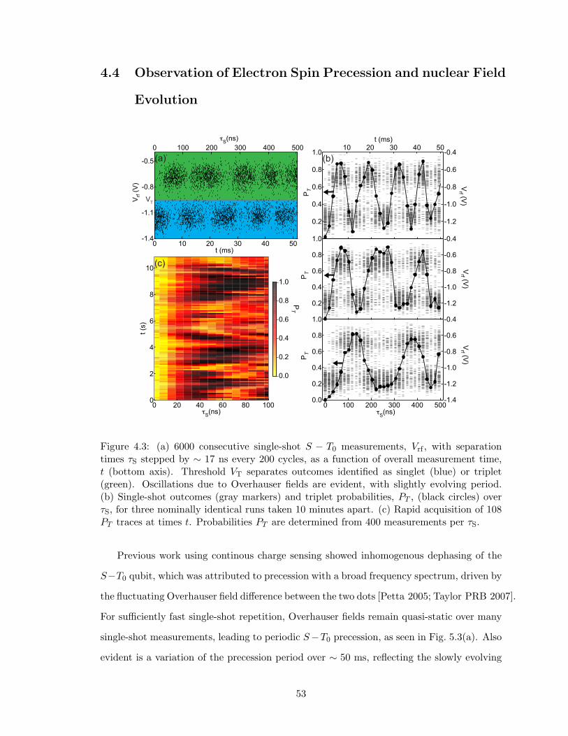
4.4 Observation of Electron Spin Precession and nuclear Field
Evolution
(a) (b)
(c)
VT
Figure 4.3: (a) 6000 consecutive single-shot S − T0 measurements, Vrf , with separationtimes τS stepped by ∼ 17 ns every 200 cycles, as a function of overall measurement time,t (bottom axis). Threshold VT separates outcomes identified as singlet (blue) or triplet(green). Oscillations due to Overhauser fields are evident, with slightly evolving period.(b) Single-shot outcomes (gray markers) and triplet probabilities, PT , (black circles) overτS, for three nominally identical runs taken 10 minutes apart. (c) Rapid acquisition of 108PT traces at times t. Probabilities PT are determined from 400 measurements per τS.
Previous work using continous charge sensing showed inhomogenous dephasing of the
S−T0 qubit, which was attributed to precession with a broad frequency spectrum, driven by
the fluctuating Overhauser field difference between the two dots [Petta 2005; Taylor PRB 2007].
For sufficiently fast single-shot repetition, Overhauser fields remain quasi-static over many
single-shot measurements, leading to periodic S−T0 precession, as seen in Fig. 5.3(a). Also
evident is a variation of the precession period over ∼ 50 ms, reflecting the slowly evolving
53
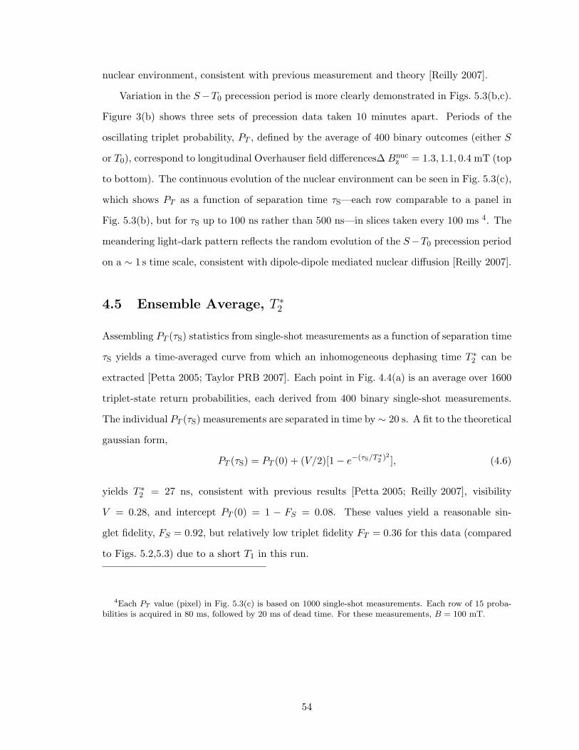
nuclear environment, consistent with previous measurement and theory [Reilly 2007].
Variation in the S−T0 precession period is more clearly demonstrated in Figs. 5.3(b,c).
Figure 3(b) shows three sets of precession data taken 10 minutes apart. Periods of the
oscillating triplet probability, PT , defined by the average of 400 binary outcomes (either S
or T0), correspond to longitudinal Overhauser field differences∆ Bnucz = 1.3, 1.1, 0.4 mT (top
to bottom). The continuous evolution of the nuclear environment can be seen in Fig. 5.3(c),
which shows PT as a function of separation time τS—each row comparable to a panel in
Fig. 5.3(b), but for τS up to 100 ns rather than 500 ns—in slices taken every 100 ms 4. The
meandering light-dark pattern reflects the random evolution of the S−T0 precession period
on a ∼ 1 s time scale, consistent with dipole-dipole mediated nuclear diffusion [Reilly 2007].
4.5 Ensemble Average, T ∗2
Assembling PT (τS) statistics from single-shot measurements as a function of separation time
τS yields a time-averaged curve from which an inhomogeneous dephasing time T ∗2 can be
extracted [Petta 2005; Taylor PRB 2007]. Each point in Fig. 4.4(a) is an average over 1600
triplet-state return probabilities, each derived from 400 binary single-shot measurements.
The individual PT (τS) measurements are separated in time by ∼ 20 s. A fit to the theoretical
gaussian form,
PT (τS) = PT (0) + (V/2)[1− e−(τS/T ∗2 )2 ], (4.6)
yields T ∗2 = 27 ns, consistent with previous results [Petta 2005; Reilly 2007], visibility
V = 0.28, and intercept PT (0) = 1 − FS = 0.08. These values yield a reasonable sin-
glet fidelity, FS = 0.92, but relatively low triplet fidelity FT = 0.36 for this data (compared
to Figs. 5.2,5.3) due to a short T1 in this run.
4Each PT value (pixel) in Fig. 5.3(c) is based on 1000 single-shot measurements. Each row of 15 proba-bilities is acquired in 80 ms, followed by 20 ms of dead time. For these measurements, B = 100 mT.
54
, B=100 mT
, B=16 mT(a) (b)
Figure 4.4: (a) Triplet probability PT as a function of separation time τS based on 1600single-shot measurements per separation time. Fit (blue curve) gives T ∗
2 = 27 ns, PT (0) =1 − FS = 0.08, V = 0.28 (see text). (b) PT as a function of separation time τI to theS − T+ anticrossing at point I. Probabilities (gray circles) based on 400 single-shot binarymeasurements. At each τI, 50 values of PT are taken 15 s apart and averaged (open blacksquares). Theory curve, Eq. (6), yields Bnuc = 0.7 mT (T ∗
2 = 37 ns), with relatively pooragreement between experiment and theory (see text).
4.6 Fast Measurement of Spin Exchange between Electron
Qubit and nuclear Bath
Finally, we investigate the triplet probability PT after separating (0,2) singlets to the point
I, where the (1,1) singlet state S crosses the T+ triplet [see Fig. 5.1(b)]. Whereas mixing of
S and T0 at point S relies on the component of the Overhauser field difference along the total
field direction, mixing of S and T+ at point I relies on the component of the Overhauser
field difference transverse to the total field. Evolution of transverse Overhauser fields are
not inhibited by nuclear or electron Zeeman energy differences, and is relatively fast, set by
nuclear dipole-dipole (∼ 100 µs) and Knight-shift (∼ 10 µs) energetics [Taylor PRB 2007;
Taylor Thesis 2007; Reilly 2007; Hanson 2007]. As expected, we do not observe periodic
precession between S and T+. We note a variation over the course of the measurement
in spin-flip probability at a fixed τI and separation point I. This is likely due to changes
in the position of the narrow S − T+ resonance resulting from a small build-up of nuclear
polarization during the measurement [Taylor Thesis 2007; Petta 2008].
Figure 4.4(b) shows probabilities PT for the T+ state as a function of τI. Each probability
value (gray circle) in Fig. 4.4(b) is based on 400 binary single-shot measurements with
τM = 8 µs. Series of PT (τI) measurements were made over a range of τI up to ∼ 100 ns,
55
with an acquisition time ∼ 50 ms per series. A total of 50 series, spaced by ∼ 15 s to allow
decorrelation of longitudinal Overhauser fields, were then averaged to give the black squares
in Fig. 4.4(b).
At small external fields, when the S − T+ anticrossing is in (1,1), the probability of
detecting a triplet following separation for a time τI can be written
PT = P 0T + V
d3B ρ(B)[(∆B2
x + ∆B2y)/2(ω/|g∗µB|)2] sin2(ωτI), (4.7)
where
ω = |g∗µB|/(2)[B2z + 2(∆B2
x + ∆B2y)]1/2 (4.8)
is the precession rate between S and T+ at the center of the anticrossing,
∆Bx(y) = [BLx(y) −BR
x(y)]/2 (4.9)
are transverse Overhauser field differences between left (L) and right (R) dots,
Bz = [BLz + BR
z ]/2 (4.10)
is the average longitudinal Overhauser field, V is readout visibility, and g∗ = −0.44 is the
effective electron g factor in GaAs. Assuming Overhauser fields B = ( ∆Bx,∆By, Bz) are
gaussian distributed on long time scales,
ρ(B) = (2πBnuc)−3/2e−(B/Bnuc)2/2, (4.11)
yields the form in Fig. 4.4(b) 5. Setting P 0T = 1− FS = 0 and Bnuc to match the overshoot
in the data yields Bnuc = 0.7 mT ∼ |g∗µBT ∗2 |−1, corresponding to T ∗
2 ∼ 40 ns, and
V = FT ∼ 0.7. Unlike Fig. 4.4(a), theory and experiment do not match well for the S − T+
5This form is expected to apply at low applied magnetic field, where the S − T+ anticrossing is in (1,1).See Eqs. (7.1)-(7.3) in Ref. [Taylor Thesis 2007]. See EPAPS Document No. E-PRLTAO-103-020943 orAppendix D for a derivation of this equation.
56
mixing, due in part to the the buildup of average nuclear polarization, which shifts the
S − T+ resonance and lowers PT .
Acknowledgments
We acknowledge support from IARPA/ARO, and the Department of Defense. Devices were
made at Harvard’s Center for Nanoscale Systems (CNS), a member of the NSF National
Nanotechnology Infrastructure Network (NNIN). We thank J. M. Taylor and E. A. Laird
for useful discussion, and J. Waissman for technical assistance.
57
Chapter 5
Fast Sensing of Double Dot ChargeArrangement and Spin State withan RF Sensor Quantum Dot
C. Barthel1 M. Kjærgaard1,2 J. Medford1 M. Stopa1 C. M. Marcus1 M. P. Hanson3 A. C.
Gossard3
1Department of Physics, Harvard University, Cambridge, Massachusetts 02138, USA
2Nano-Science Center, Niels Bohr Institute, University of Copenhagen, Universitetsparken
5, DK-2100 Copenhagen, Denmark
3Materials Department, University of California, Santa Barbara, California 93106, USA
Single-shot measurement of the charge arrangement and spin state of a double quantum
dot are reported, with measurement times down to ∼100 ns. Sensing uses radio-frequency
reflectometry of a proximal quantum dot in the Coulomb blockade regime. The sensor quan-
tum dot is up to 30 times more sensitive than a comparable quantum point contact sensor,
and yields three times greater signal to noise in rf single-shot measurements. Numerical
modeling is qualitatively consistent with experiment and shows that the improved sensitivity
of the sensor quantum dot results from reduced screening and lifetime broadening 1.
1This chapter is adapted from Ref. [Barthel SQD 2010] with permission, c(2010) by the AmericanPhysical Society
58
5.1 Introduction
Experiments on few-electron quantum dots [Hanson 2007], including spin qubits, have ben-
efitted in recent years from the use of proximal charge sensing, a technique that allows the
number and arrangement of charges confined in nanostructures to be measured via changes
in conductance of a nearby sensor to which the device of interest is capacitively coupled
[Field 1993; Ihn 2009]. Quantum point contacts (QPCs) have been widely used as charge
sensors, allowing, for instance, high-fidelity single-shot readout of spin qubits via spin-to-
charge conversion [Elzerman 2004; Barthel 2009]. Single electron transistors (SETs) based
on metallic tunnel junctions, and gate defined sensor quantum dots (SQD), conceptually
equivalent to SETs, have also been widely used as proximal sensors, and provide similar
sensitivity and bandwidth [Schoelkopf 1998; Buehler 2005; Lu 2003; Fujisawa 2004]. As a
typical application, measuring the state of a spin qubit via spin-to-charge conversion involves
determining whether two electrons in a double quantum dot are in the (1, 1) or the (0, 2)
charge configuration, where (left, right) denotes occupancies in the double dot [Fig. 1(a)],
on time scales faster than the spin relaxation time [Barthel 2009].
In this chapter, we demonstrate the use of a sensor quantum dot for fast charge and two-
electron spin-state measurement in a GaAs double quantum dot, biased near the (1,1)-(0,2)
charge transition. We compare the performance of the SQD to conventional quantum point
contact (QPC) sensors for dc and radio-frequency (rf) measurement. We find experimentally
that the SQD is up to 30 times more sensitive, and provides roughly three times the signal
to noise ratio (SNR) of a comparable QPC sensor for detecting the charge arrangement
and spin state of a double quantum dot. Numerical simulations, also presented, give results
consistent with experiment and elucidate the role of screening in determining the sensitivity
of these proximal charge sensors.
5.2 Device and Measurement Setup
Double quantum dots with integrated sensors are defined by Ti/Au depletion gates on
a GaAs/Al0.3Ga0.7As heterostructure with a two-dimensional electron gas (density 2 ×
1015 m−2, mobility 20 m2/Vs) 100 nm below the surface. The charge state of the double
59
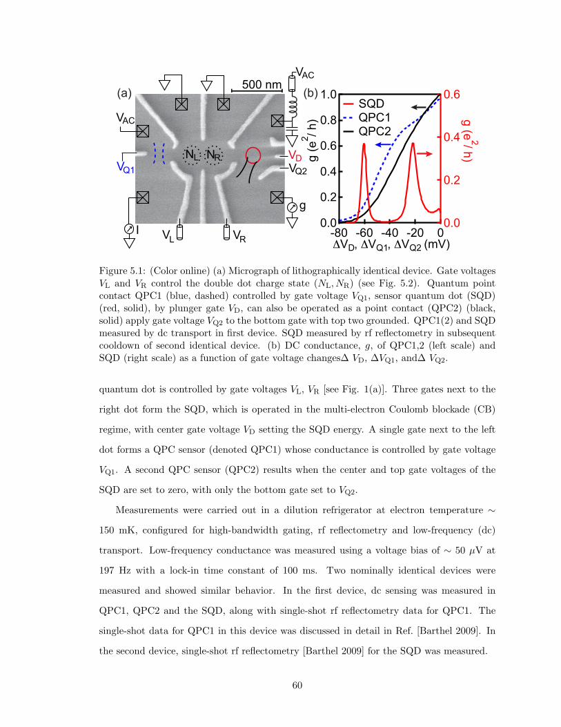
V VL R
500 nm
VAC
VQ2VQ1VD
I
g
N NL R
2
FIG.1:(Coloronline)(a)Schematicofmeasurementsetupincludingfalse-colorSEMimageofarepresentativedevice.Gatesshadedgreenareheldat∼1Vthroughout.Niobiumcoaxand∼50Ωohmiccontactsminimizelossesbetweensampleandcryogenicamplifier.AstriplinefabricatedonasapphiresubstrateisusedtothermalizetheinnerconductoroftheNbcoax.DemodulationisperformedbymixingtheRFsignalwithalocaloscillator(LO)toyieldaninterme-diatefrequency(IF)thatislow-passfiltered(LPF)beforefurtheramplificationanddigitization.(b)Photographofrfcircuitboardshowingsample,matchingcircuitandcompo-nentsusedtomakeabias-Tee.(c)ReflectioncoefficientS11ofimpedancetransformerwithchanginggQPC(resonanceat220.2MHz).(d)Demodulatedresponse(Vrf)measuredsi-multaneouslywithdcconductanceastheQPCgate(shadedblueinSEMimage)biasisvaried(VL=-700mV).Dashedlineindicatesbiaspointforchargesensing.InsetshowstransferfunctionofVrfversesconductance.(e)Demodulatedtime-domainresponseto50MHzgatesignalwithQPCbiasedto∼e2/handmatchinginductancereducedto560nH(differentdevicetoallothermeasurementspresented).
FIG.2:(Coloronline)(a)AMresponseofrf-QPCto1MHzgatemodulation,VR=0.7mV(rms).SNRofsidebandsyieldsasensitivitySg=5×10⁻⁶e2/hHz−1/2.(b)SNRofuppersidebandasafunctionofmodulationfrequency.Redcurveisaguidetotheeye.(c)SNRofuppersidebandasafunctionofcarrierpower.(d)SNRofuppersidebandasafunctionofcarrierfrequency,consistentwithFig.1(c).AllSNRmeasurementsmadeinaresolutionbandwidthof∆f=10kHz.
FIG.3:(Coloronline)(a)DerivativeofVrf(inarbitaryunits)asafunctionofVLandVR,magneticfieldB=100mT.VL
israsteredat∼1mV/150µs(∼106datapointsacquiredin∼180s).Labelsindicatenumberofelectronsintheleftandrightdots.
width∆f.ThisSNRgivesaconductancesensitivitySg=(1/2)dgQPC(∆f)−1/210−SNR/20,wherethefactor1/2accountsforpowercollectedfrombothsidebands,of5×10−6e2/hHz−1/2.Thissensitivityallows,forinstance,adgQPC=0.01e2/hconductancechangetobemeasuredwithunitySNRinτint=500ns.Above∼8MHz,theQ-factor(∼15)oftheimpedancematchingcircuitlimitsthesensitivityasshowninFig.2(b).TheSNRincreaseswithappliedcarrierpower[Fig.2(c)]uptotheenergy
VAC
(b)(a)
Figure 5.1: (Color online) (a) Micrograph of lithographically identical device. Gate voltagesVL and VR control the double dot charge state (NL, NR) (see Fig. 5.2). Quantum pointcontact QPC1 (blue, dashed) controlled by gate voltage VQ1, sensor quantum dot (SQD)(red, solid), by plunger gate VD, can also be operated as a point contact (QPC2) (black,solid) apply gate voltage VQ2 to the bottom gate with top two grounded. QPC1(2) and SQDmeasured by dc transport in first device. SQD measured by rf reflectometry in subsequentcooldown of second identical device. (b) DC conductance, g, of QPC1,2 (left scale) andSQD (right scale) as a function of gate voltage changes∆ VD, ∆VQ1, and∆ VQ2.
quantum dot is controlled by gate voltages VL, VR [see Fig. 1(a)]. Three gates next to the
right dot form the SQD, which is operated in the multi-electron Coulomb blockade (CB)
regime, with center gate voltage VD setting the SQD energy. A single gate next to the left
dot forms a QPC sensor (denoted QPC1) whose conductance is controlled by gate voltage
VQ1. A second QPC sensor (QPC2) results when the center and top gate voltages of the
SQD are set to zero, with only the bottom gate set to VQ2.
Measurements were carried out in a dilution refrigerator at electron temperature ∼
150 mK, configured for high-bandwidth gating, rf reflectometry and low-frequency (dc)
transport. Low-frequency conductance was measured using a voltage bias of ∼ 50 µV at
197 Hz with a lock-in time constant of 100 ms. Two nominally identical devices were
measured and showed similar behavior. In the first device, dc sensing was measured in
QPC1, QPC2 and the SQD, along with single-shot rf reflectometry data for QPC1. The
single-shot data for QPC1 in this device was discussed in detail in Ref. [Barthel 2009]. In
the second device, single-shot rf reflectometry [Barthel 2009] for the SQD was measured.
60
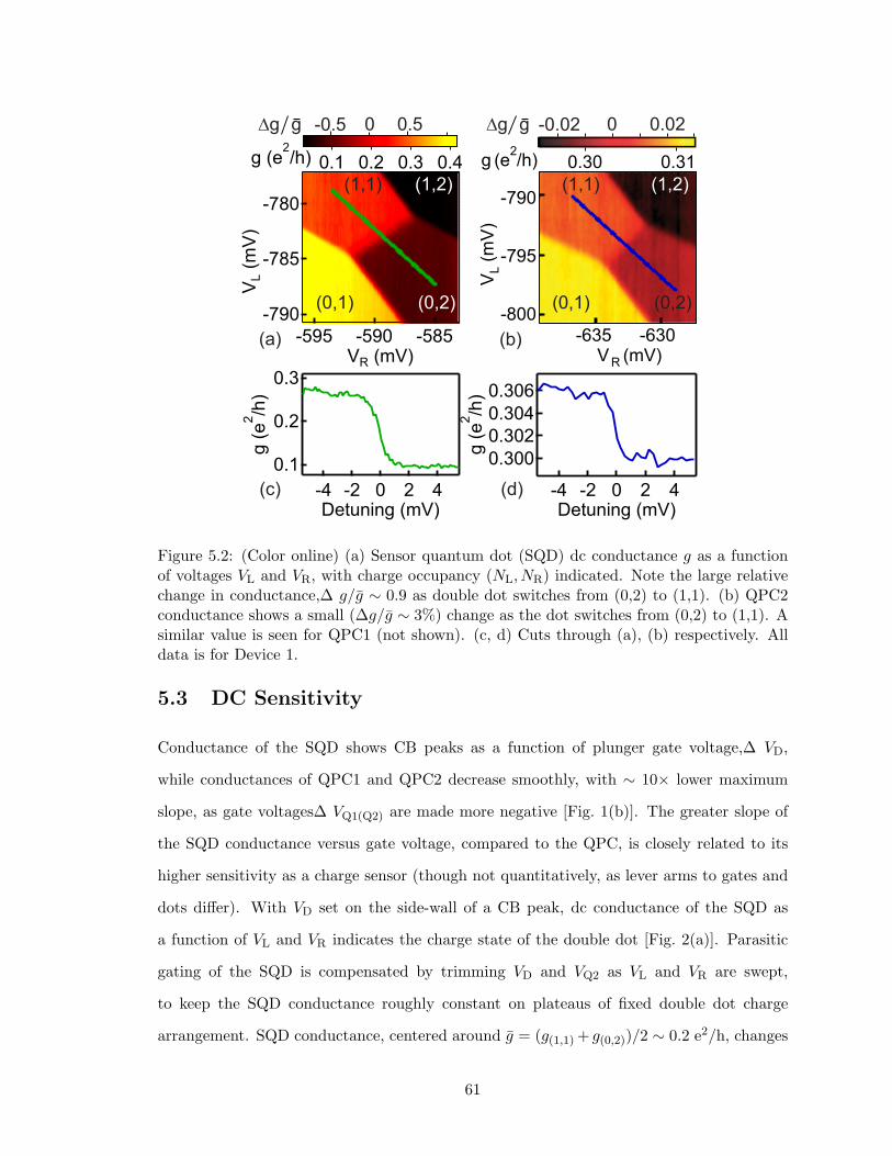
(b)(a)
(0,2)(0,1)
(1,2)
0 0.02-0.02
(c) (d)
(1,1)
0.306
0.304
0.302
0.300g
(e
2/h
)-4 -2 0 2 4Detuning (mV)
0.3
0.2
0.1
g (
e2/h
)
-4 -2 0 2 4Detuning (mV)
0 0.5-0.5
(0,2)(0,1)
(1,2)(1,1)
Figure 5.2: (Color online) (a) Sensor quantum dot (SQD) dc conductance g as a functionof voltages VL and VR, with charge occupancy (NL, NR) indicated. Note the large relativechange in conductance,∆ g/g ∼ 0.9 as double dot switches from (0,2) to (1,1). (b) QPC2conductance shows a small (∆g/g ∼ 3%) change as the dot switches from (0,2) to (1,1). Asimilar value is seen for QPC1 (not shown). (c, d) Cuts through (a), (b) respectively. Alldata is for Device 1.
5.3 DC Sensitivity
Conductance of the SQD shows CB peaks as a function of plunger gate voltage,∆ VD,
while conductances of QPC1 and QPC2 decrease smoothly, with ∼ 10× lower maximum
slope, as gate voltages∆ VQ1(Q2) are made more negative [Fig. 1(b)]. The greater slope of
the SQD conductance versus gate voltage, compared to the QPC, is closely related to its
higher sensitivity as a charge sensor (though not quantitatively, as lever arms to gates and
dots differ). With VD set on the side-wall of a CB peak, dc conductance of the SQD as
a function of VL and VR indicates the charge state of the double dot [Fig. 2(a)]. Parasitic
gating of the SQD is compensated by trimming VD and VQ2 as VL and VR are swept,
to keep the SQD conductance roughly constant on plateaus of fixed double dot charge
arrangement. SQD conductance, centered around g = (g(1,1) + g(0,2))/2 ∼ 0.2 e2/h, changes
61
by∆ gSQD ∼ 0.2 e2/h when the double dot charge arrangement changes from (0, 2) to (1, 1)
(Fig. 2(c),. Figure 2(d) shows corresponding 2 changes in QPC2 conductance, which changes
by∆ gQPC2 ∼ 0.01 e2/h around g ∼ 0.3 e2/h for the same charge rearrangement, consistent
with values in the literature. The ratio of conductance changes,∆ gSQD/∆gQPC2 ∼ 30, is a
measure of the relative sensitivity of SQD and QPC2 to the double dot charge state.
5.4 Fast Single-shot Measurements
To demonstrate fast measurement of a spin qubit via spin-to-charge conversion, the SQD is
configured as the resistive element in an rf reflectometry circuit [Reilly APL 2007], following
Ref. [Barthel 2009], and biased via VD on the sidewall of a CB peak. The reflected rf
amplitude, vrf , tracks SQD conductance. Gate pulses applied to VL and VR first prepare
the ground state singlet in (0, 2), then separate the spins by moving to point S, deep in
(1, 1), for a time τS = 1−200 ns 3, allowing precession between (1, 1)S and (1, 1)T0 driven by
hyperfine fields, then move to the measurement point M in (0,2) for τmaxM = 5 µs (Fig. 2(a)
and Ref. [Barthel 2009]). At M, only the singlet configuration of the two spins can rapidly
move to the (0,2) ground state; spin triplets remain trapped in (1, 1) for the spin relaxation
time [Barthel 2009].
With rf excitation applied to the SQD only during the measurement interval at point M,
the reflectometry signal, vrf , is digitally integrated over a subinterval of duration τM to yield
a single-shot measurement outcome Vrf . From histograms of 3×10⁴ Vrf measurements (with
0.7 mV binning), probabilities, P , of single-shot outcomes can be estimated for each value of
τM. As seen in Figs. 3(a,b), measurement noise decreases with increasing integration time,
allowing distinct peaks—indicating singlet [i.e., (0,2)] and triplet [i.e., (1,1)] outcomes—to
be distinguished for τM > 100 ns. The difference between singlet and triplet output voltages,
2Adjusting VQ2 and VD to switch between a QPC and a SQD, shifts the charge stability diagram by∼ 30 mV.
3The separation time τS is stepped from 1 to 200 ns, every 1000 cycles for a total of 30,000 cycles.
62
the signal
∆V = V Trf − V S
rf (5.1)
reflects the rf sensitivity of the SQD to the single-charge motion from (1,1) to (0,2).
Experimental P (Vrf) curves for the SQD are in good agreement with theoretical mod-
els [Barthel 2009], as shown in Fig. 3(b). Fits of the model give values for the spin relaxation
time, T1 = 13 µs, the mean triplet probability, PT = 0.46, the peak width, σrf , and the
peak positions, V Srf and V T
rf . The resulting signal to noise ratio,
SNR = ∆V/σrf (5.2)
is shown in Fig. 3(c) as a function of τM, along with the SNR for QPC1. A direct comparison
must take into account that the SQD data in all panels of Fig. 3 used -99 dBm applied rf
power (∼ 0.15 mV), while the QPC1 data in Fig. 3(c) used -89 dBm applied rf power
(∼ 0.45 mV), values chosen to maximize the SNR for each. For both QPC1 and SQD, the
output signal∆ V saturated at higher powers, due in part to broadening of the conductance
features due to heating and finite bias.
SNR for both the SQD and QPC1 improve with increasing integration time, as shown
in Fig. 3(c). Fitting the measured SQD signal to noise ratios to the form Eq. 5.2, with
σrf = σ0
1µs/(τM + τ0), (5.3)
yields an intrinsic integration time, τ0 = 190 ns, due to the ∼ 1.5 MHz bandwidth of the
reflectometry circuit, a signal,∆ VSQD = 33 mV, and a characteristic width, σ0 = 5 mV, the
measurement noise for one microsecond total integration time. The ratio∆ V/σ0 represents
a characteristic SNR, which is 6.6 for this SQD. A similar measurement of the characteristic
SNR for QPC1, at 10 dB higher applied rf power, yields a value 2.2 4, with ∆VQPC1 = 10 mV
and σ0 = 4.5 mV.
4For QPC1 in Ref. [Barthel 2009], the fit parameters for the histograms, are T1 = 34 µs, τ0 = 700 ns,and PT ∼ 0.5.
63
For both SQD and QPC1, analysis [Korotkov 1999] predicts signals,∆ V , consistent
with measured values, and widths, σ0, due to shot noise that are considerably lower than
the measured peak widths. Specifically, σ0 ∼ 1.5(3) mV and ∼ 3 mV are expected for SQD
(QPC1) 5. This is roughly one tenth (half) of the total noise for the SQD (QPC1). The
remaining measurement noise for both sensors is due to charge-, gate- and instrumenta-
tion noise, predominantly from the cryogenic amplifier5 [Reilly APL 2007]. We conclude,
based on the single-shot data, that the measured SQD offers improved SNR compared to
a comparable QPC sensor, SNRSQD/SNRQPC1 ∼ 3. The improvement is not as large as
the relative improvement in sensitivity at dc,∆ gSQD/∆gQPC1 ∼ 10, mainly due to a lower
rf power saturation of the SQD SNR and the experimental noise floor of the measurement
setup.
5.5 Numerical Simulation
To investigate QPC and SQD performance numerically, we consider the sensitivity, s, as
the change in conductance in response to a change in voltage, either applied to a gate or
arising from a charge rearrangement. Modeling the specific device geometry, for QPC1,
sQPC ≡∂g
∂VQ1=
∂g
∂φSP
∂φSP
∂VQ1, (5.4)
where φSP is the electrostatic potential at the saddle point of QPC1. For the SQD,
sSQD ≡∂g
∂VD=
∂g
∂φdot
∂φdot
∂VD, (5.5)
where φdot is the electrostatic potential in the center of the SQD.
For the QPC, the conductance, g, and its derivative with respect to potential, is calcu-
lated as a thermal average over the transmission probability, following Ref. [Fertig 1987].
5The contribution from thermal fluctuations to intrinsic sensor noise is negligible. The cryogenic amplifiercontributes 60% (40%) of the total noise for SQD (QPC1).
64
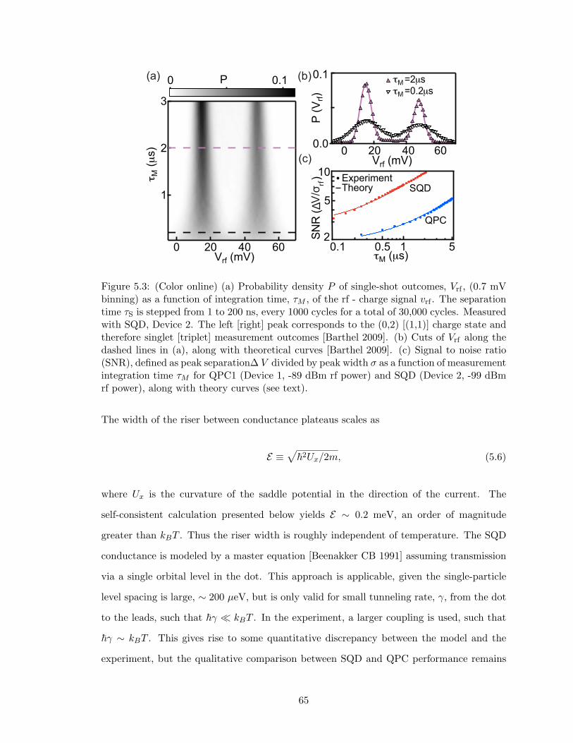
0.1
0.0
P (V
rf)
6040200Vrf (mV)
(a) (b)
2
5
10
M =2 sM =0.2 s
510.50.1 M ( s)
SNR
(
)rf
ExperimentTheory SQD
QPC
(c)
6040200Vrf (mV)
3
2
1
M (µ
s)
0.100.050 P
Figure 5.3: (Color online) (a) Probability density P of single-shot outcomes, Vrf , (0.7 mVbinning) as a function of integration time, τM , of the rf - charge signal vrf . The separationtime τS is stepped from 1 to 200 ns, every 1000 cycles for a total of 30,000 cycles. Measuredwith SQD, Device 2. The left [right] peak corresponds to the (0,2) [(1,1)] charge state andtherefore singlet [triplet] measurement outcomes [Barthel 2009]. (b) Cuts of Vrf along thedashed lines in (a), along with theoretical curves [Barthel 2009]. (c) Signal to noise ratio(SNR), defined as peak separation∆ V divided by peak width σ as a function of measurementintegration time τM for QPC1 (Device 1, -89 dBm rf power) and SQD (Device 2, -99 dBmrf power), along with theory curves (see text).
The width of the riser between conductance plateaus scales as
E ≡
2Ux/2m, (5.6)
where Ux is the curvature of the saddle potential in the direction of the current. The
self-consistent calculation presented below yields E ∼ 0.2 meV, an order of magnitude
greater than kBT . Thus the riser width is roughly independent of temperature. The SQD
conductance is modeled by a master equation [Beenakker CB 1991] assuming transmission
via a single orbital level in the dot. This approach is applicable, given the single-particle
level spacing is large, ∼ 200 µeV, but is only valid for small tunneling rate, γ, from the dot
to the leads, such that γ kBT . In the experiment, a larger coupling is used, such that
γ ∼ kBT . This gives rise to some quantitative discrepancy between the model and the
experiment, but the qualitative comparison between SQD and QPC performance remains
65
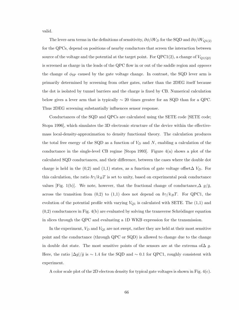
valid.
The lever-arm terms in the definitions of sensitivity, ∂φ/∂VD for the SQD and ∂φ/∂VQ1(2)
for the QPCs, depend on positions of nearby conductors that screen the interaction between
source of the voltage and the potential at the target point. For QPC1(2), a change of VQ1(Q2)
is screened as charge in the leads of the QPC flow in or out of the saddle region and opposes
the change of φSP caused by the gate voltage change. In contrast, the SQD lever arm is
primarily determined by screening from other gates, rather than the 2DEG itself because
the dot is isolated by tunnel barriers and the charge is fixed by CB. Numerical calculation
below gives a lever arm that is typically ∼ 20 times greater for an SQD than for a QPC.
Thus 2DEG screening substantially influences sensor response.
Conductances of the SQD and QPCs are calculated using the SETE code [SETE code;
Stopa 1996], which simulates the 3D electronic structure of the device within the effective-
mass local-density-approximation to density functional theory. The calculation produces
the total free energy of the SQD as a function of VD and N , enabling a calculation of the
conductance in the single-level CB regime [Stopa 1993]. Figure 4(a) shows a plot of the
calculated SQD conductances, and their difference, between the cases where the double dot
charge is held in the (0,2) and (1,1) states, as a function of gate voltage offset∆ VD. For
this calculation, the ratio γ/kBT is set to unity, based on experimental peak conductance
values [Fig. 1(b)]. We note, however, that the fractional change of conductance,∆ g/g,
across the transition from (0,2) to (1,1) does not depend on γ/kBT . For QPC1, the
evolution of the potential profile with varying VQ1 is calculated with SETE. The (1,1) and
(0,2) conductances in Fig. 4(b) are evaluated by solving the transverse Schrodinger equation
in slices through the QPC and evaluating a 1D WKB expression for the transmission.
In the experiment, VD and VQ1 are not swept, rather they are held at their most sensitive
point and the conductance (through QPC or SQD) is allowed to change due to the change
in double dot state. The most sensitive points of the sensors are at the extrema of∆ g.
Here, the ratio |∆g|/g is ∼ 1.4 for the SQD and ∼ 0.1 for QPC1, roughly consistent with
experiment.
A color scale plot of the 2D electron density for typical gate voltages is shown in Fig. 4(c).
66
0.0
0.5
-0.4
-0.2
0.2
0.4
0.0
0.0-0.5-1.0-1.5-2.0-2.5-3.0V (mV) 500 nm
0
2.5
5
g (e
/h)
2
(a)g(0,2)g(1,1)
gn (10
10cm-2)
g (e /h)2
(c)
D
(b)
2
Figure 5.4: (Color online) (a) Conductance (simulation) through the SQD as function ofthe gate voltage VD, for the two double dot charge-states (1, 1) and (0, 2). (b) Conductancethrough QPC1 at 5 mV intervals (lines are guide to the eye). (c) Electron density profile fortypical gate voltages in the (1,1) configuration, with superimposed micrograph of device.The color scale is centered near 2.5 × 1010cm−2 to accentuate the charge in the dots andthe saddle point of QPC1.
5.6 Conclusion
In conclusion, by taking advantage of the increased sensitivity and SNR of a sensor quantum
dot in the CB regime (compared to a proximal QPC), we have demonstrated single-shot spin-
to-charge readout of a few-electron double quantum dot in∼ 100 ns 6 with SNR ∼ 3 (Fig. 3),
representing an order of magnitude improvement over previous results [Barthel 2009]. Nu-
merical simulation based on density functional theory yields good qualitative agreement
with experiment, and elucidates key differences between a quantum dot and a QPC as a
proximal charge sensor. Reduced screening and smaller characteristic energy needed to
change transmission in the quantum dot compared to the QPC are responsible for its im-
6The measurement time is limited by the measurement bandwidth, not the time needed to obtain a SNRof unity.
67
proved performance.
Acknowledgments
We acknowledge funding from ARO/iARPA, the Department of Defense and IBM. MK ac-
knowledges support from Augustinus Foundation, Højgaard Foundation and Stefan Rozental
and Hanna Kobylinski Rozental Foundation. This work was performed in part at the Cen-
ter for Nanoscale Systems (CNS), a member of the National Nanotechnology Infrastructure
Network (NNIN), which is supported by the National Science Foundation under NSF award
no. ECS-0335765. Computational support from the NNIN computation project (NNIN/C)
is gratefully acknowledged. We thank Hendrik Bluhm, Edward Laird and David Reilly for
useful discussion.
68
Chapter 6
Singlet-Triplet Qubit Relaxationand Initialization in a magneticField Gradient
C. Barthel1,3 J. Medford1,3 H. Bluhm1 A. Yacoby1 C. M. Marcus1 M. P. Hanson2 A. C. Gossard2
1Department of Physics, Harvard University, Cambridge, Massachusetts 02138, USA
2Materials Department, University of California, Santa Barbara, California 93106, USA
3 These authors contributed equally to this work.
The measurement visibility and triplet relaxation time, T1, of a singlet-triplet qubit in
a double quantum dot are studied as function of magnetic field gradients induced by spin
polarization of GaAs nuclei. For applied magnetic fields between 10 mT and 2 T, a nuclear
field gradient is always observed after a nuclear polarization pump-cycle. The field gradient
results in a reduced visibility of measured singlet-triplet precessions, which for long time
averages reproduces the phenomenology previously attributed to a suppression of singlet-
triplet dephasing. Performing fast measurements, with a high sensitivity sensor quantum
dot (SQD), we study the dependence of the triplet relaxation time during measurement on
magnetic field gradient, gate voltage configuration during measurement and applied mag-
netic field. We develop a simple model describing charge relaxation after singlet-triplet
mixing that agrees well with the data. The initialization fidelity of a singlet decreases with
increasing field gradients, presumably due to finite times over which the system is sepa-
rated into two dots, and recombined into one dot. We intentionally reduce the initialization
69
fidelity in S − T0 precession experiments, thereby performing a weak measurement of the
nuclear magnetic field gradient. The findings are relevant for quantum information process-
ing, where high measurement and initialization fidelities in the presence of magnetic field
gradients are desired 1.
1This chapter is adapted from a manuscript in preparation for submission [Barthel T1 2010].
70
6.1 Introduction
Spin states of confined electrons are of interest for the investigation of basic quantum
mechanics, decoherence and controlled entanglement, as probes of mesoscopic nuclear spin
environments, and as qubits in quantum information processing [Loss 1998]. The singlet-
triplet basis of a pair of electron spins in two coupled quantum dots has been suggested
as a logical qubit, as it is inherently protected against collective dephasing [Levy 2002].
Sub-nanosecond operations on the qubit have been realized, using the exchange energy
between singlet and triplet states to perform rotations around one of the qubit bloch sphere
axes [Petta 2005]. Qubit rotations around a second independent axis, needed for universal
control, can be induced by a magnetic field difference between the two quantum dots. A
field difference for these rotations can be realized via a micro magnet on top of the double
dot [Pioro-Ladriere 2007], and has recently been realized via a gradient in the nuclear
polarization of the host material [Foletti 2009]. Fast measurement of a qubit state has
been demonstrated for two-electron spin states [Meunier 2006; Barthel 2009], as well as for
single-electron spin states [Elzerman 2004; Amasha 2008].
Aside from being a useful tool to manipulate the qubit, the Overhauser fields from the
nuclei also are the major source of qubit decoherence [Petta 2005]. The interaction between
electron spins and nuclear spins in GaAs has been studied optically [Paget 1977] and in
electronic transport measurements where the nuclear spin state showed hysteretic behav-
ior and strongly influenced the electronic properties [Ono 2004; Baugh 2007]. In pulsed
measurements, the time evolution and statistics of polarized and unpolarized nuclear states
have been studied [Reilly Diff. 2008; Reilly 2007], and the nuclear spins have been identified
as a mechanism of electron spin relaxation [Johnson Nature 2005]. Spin relaxation limits
the fidelity of qubit measurement [Barthel 2009], therefore it is important to understand
how magnetic field gradients, from micro-magnets or nuclear polarizations, affect the qubit
relaxation time at the readout stage.
In Ref. [Reilly 2008], it was observed that a nuclear pump-cycle, exchanging spin be-
tween the electrons and the nuclear bath, increased the probability, PS , to measure a sin-
glet outcome after evolution of a separated singlet state, which is sensitive to nuclear field
71
gradients. It was conjectured that the pump-cycle reduced the fluctuating nuclear field dif-
ference between the two quantum dots by preparing a special nuclear state, stable over long
time scales. This interpretation is consistent with various theoretical works [Ramon 2007;
Ribeiro 2008; Stopa 2010], while other experimental and theoretical work suggest that nu-
clear pump-cycles generally build up field gradients [Foletti 2009; Gulland 2010].
In this chapter, we suggest an alternative explanation for the increased singlet measure-
ment probability observed in Ref. [Reilly 2008], based on a nuclear field gradient induced
reduction of the triplet relaxation time, resulting in vanishing measurement visibility for
large nuclear polarizations. We investigate the buildup of nuclear polarization by electrical
pump-cycles for a range of directions and magnitudes of applied magnetic field and find that
for all investigated experimental parameters, a gradient in nuclear polarization is induced
together with an average polarization.
A reduction in the visibility of measured singlet-triplet precessions with increasing nu-
clear field gradient is observed for all parameters. The visibility is studied as function of
nuclear field gradient, applied magnetic field, and gate voltage configuration during the
measurement. Simultaneously, the triplet relaxation time at the measurement point is
measured in time domain. The dominant part of the visibility reduction for large nuclear
polarizations is due to an increased triplet relaxation rate during the measurement, inde-
pendent of applied magnetic field. We find good agreement with a simple model describing
triplet decay, via charge relaxation after singlet-triplet mixing driven by the field difference.
By introducing a ramp-time, over which an initial singlet state is separated to occupy two
dots and recombined into one dot after evolution, we intentionally reduce the initialization
fidelity in S − T0 precession experiments. Thereby a weak measurement of the nuclear
magnetic field gradient is performed. The precession data as function of ramp-time gives
evidence that a finite pulse rise-time decreases the initialization and readout fidelity of the
qubit in the presence of nuclear polarization.
The remainder of this chapter is organized as follows. In section 6.2 we discuss the
double dot system under investigation and the technical setup. The theory of the two
electron qubit system, the nuclear pumping and the probe-cycle, as employed in previous
72
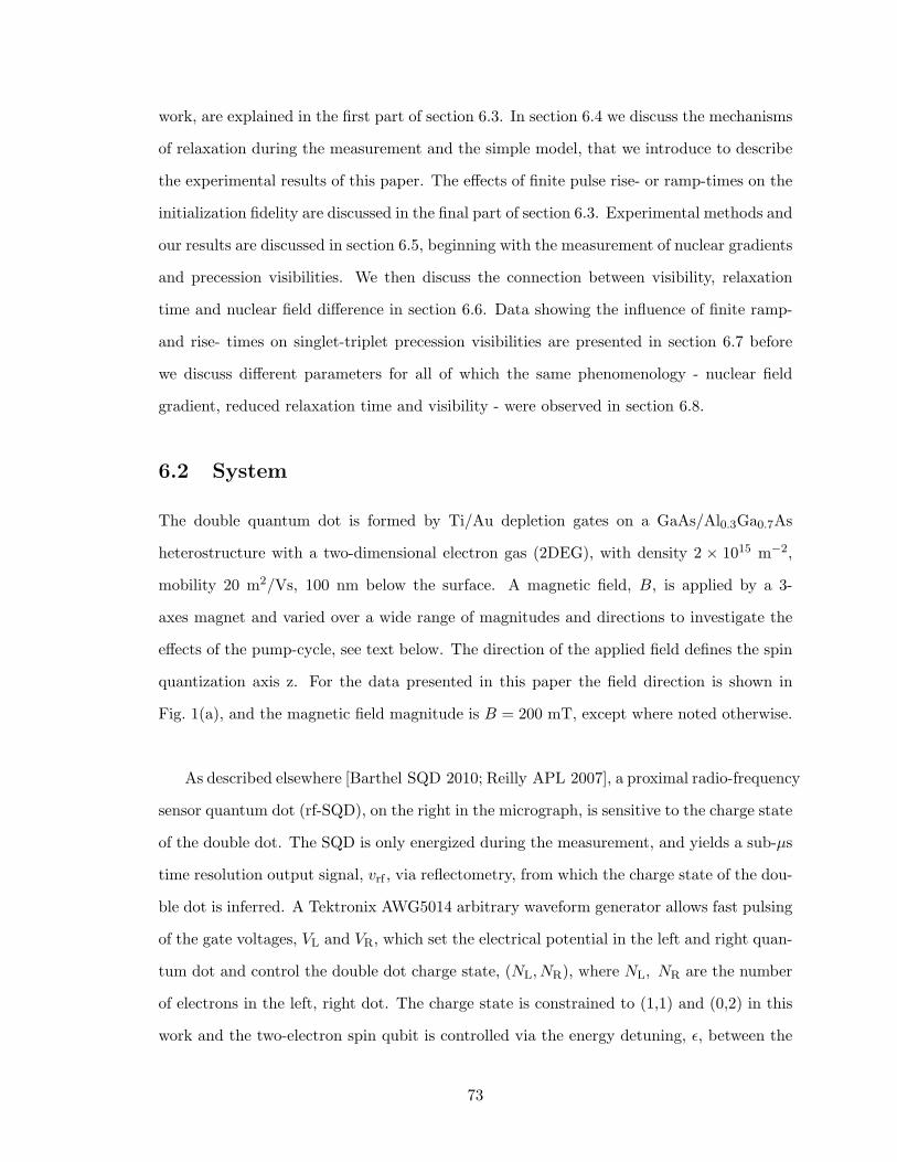
work, are explained in the first part of section 6.3. In section 6.4 we discuss the mechanisms
of relaxation during the measurement and the simple model, that we introduce to describe
the experimental results of this paper. The effects of finite pulse rise- or ramp-times on the
initialization fidelity are discussed in the final part of section 6.3. Experimental methods and
our results are discussed in section 6.5, beginning with the measurement of nuclear gradients
and precession visibilities. We then discuss the connection between visibility, relaxation
time and nuclear field difference in section 6.6. Data showing the influence of finite ramp-
and rise- times on singlet-triplet precession visibilities are presented in section 6.7 before
we discuss different parameters for all of which the same phenomenology - nuclear field
gradient, reduced relaxation time and visibility - were observed in section 6.8.
6.2 System
The double quantum dot is formed by Ti/Au depletion gates on a GaAs/Al0.3Ga0.7As
heterostructure with a two-dimensional electron gas (2DEG), with density 2 × 10¹⁵ m−2,
mobility 20 m2/Vs, 100 nm below the surface. A magnetic field, B, is applied by a 3-
axes magnet and varied over a wide range of magnitudes and directions to investigate the
effects of the pump-cycle, see text below. The direction of the applied field defines the spin
quantization axis z. For the data presented in this paper the field direction is shown in
Fig. 1(a), and the magnetic field magnitude is B = 200 mT, except where noted otherwise.
As described elsewhere [Barthel SQD 2010; Reilly APL 2007], a proximal radio-frequency
sensor quantum dot (rf-SQD), on the right in the micrograph, is sensitive to the charge state
of the double dot. The SQD is only energized during the measurement, and yields a sub-µs
time resolution output signal, vrf , via reflectometry, from which the charge state of the dou-
ble dot is inferred. A Tektronix AWG5014 arbitrary waveform generator allows fast pulsing
of the gate voltages, VL and VR, which set the electrical potential in the left and right quan-
tum dot and control the double dot charge state, (NL, NR), where NL, NR are the number
of electrons in the left, right dot. The charge state is constrained to (1,1) and (0,2) in this
work and the two-electron spin qubit is controlled via the energy detuning, , between the
73
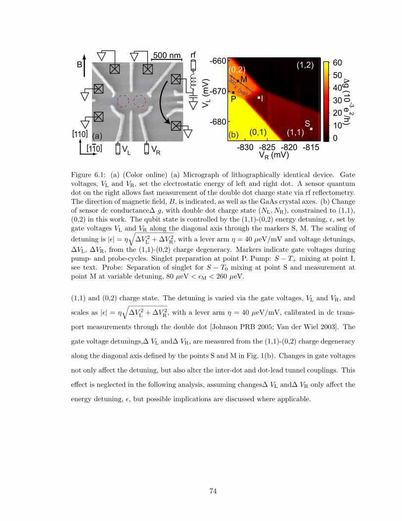
VL VR
500 nm rfB
[110]
[110]
-680
-670
-660
VL (
mV
)
-830 -825 -820 -815VR (mV)
60
50
40
30
20
10
0
g (1
0-3e
2/h)
(0,1)
(1,2)
(1,1)
(0,2)M
I
S
300 ( eV)
P
(a) (b)
Figure 6.1: (a) (Color online) (a) Micrograph of lithographically identical device. Gatevoltages, VL and VR, set the electrostatic energy of left and right dot. A sensor quantumdot on the right allows fast measurement of the double dot charge state via rf reflectometry.The direction of magnetic field, B, is indicated, as well as the GaAs crystal axes. (b) Changeof sensor dc conductance∆ g, with double dot charge state (NL, NR), constrained to (1,1),(0,2) in this work. The qubit state is controlled by the (1,1)-(0,2) energy detuning, , set bygate voltages VL and VR along the diagonal axis through the markers S, M. The scaling ofdetuning is || = η
∆V 2
L + ∆V 2R , with a lever arm η = 40 µeV/mV and voltage detunings,
∆VL, ∆VR, from the (1,1)-(0,2) charge degeneracy. Markers indicate gate voltages duringpump- and probe-cycles. Singlet preparation at point P. Pump: S − T+ mixing at point I,see text. Probe: Separation of singlet for S − T0 mixing at point S and measurement atpoint M at variable detuning, 80 µeV < M < 260 µeV.
(1,1) and (0,2) charge state. The detuning is varied via the gate voltages, VL and VR, and
scales as || = η
∆V 2L + ∆V 2
R , with a lever arm η = 40 µeV/mV, calibrated in dc trans-
port measurements through the double dot [Johnson PRB 2005; Van der Wiel 2003]. The
gate voltage detunings,∆ VL and∆ VR, are measured from the (1,1)-(0,2) charge degeneracy
along the diagonal axis defined by the points S and M in Fig. 1(b). Changes in gate voltages
not only affect the detuning, but also alter the inter-dot and dot-lead tunnel couplings. This
effect is neglected in the following analysis, assuming changes∆ VL and∆ VR only affect the
energy detuning, , but possible implications are discussed where applicable.
74
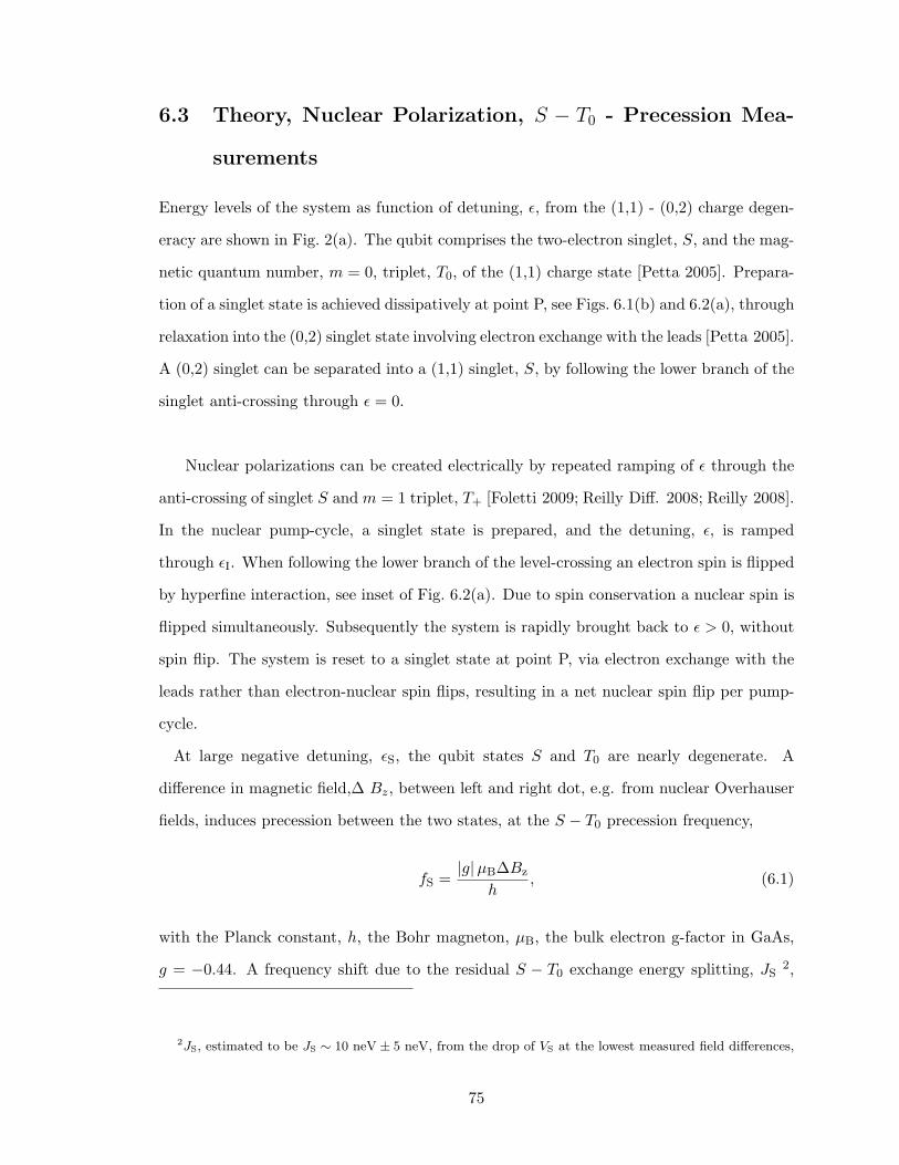
6.3 Theory, Nuclear Polarization, S − T0 - Precession Mea-
surements
Energy levels of the system as function of detuning, , from the (1,1) - (0,2) charge degen-
eracy are shown in Fig. 2(a). The qubit comprises the two-electron singlet, S, and the mag-
netic quantum number, m = 0, triplet, T0, of the (1,1) charge state [Petta 2005]. Prepara-
tion of a singlet state is achieved dissipatively at point P, see Figs. 6.1(b) and 6.2(a), through
relaxation into the (0,2) singlet state involving electron exchange with the leads [Petta 2005].
A (0,2) singlet can be separated into a (1,1) singlet, S, by following the lower branch of the
singlet anti-crossing through = 0.
Nuclear polarizations can be created electrically by repeated ramping of through the
anti-crossing of singlet S and m = 1 triplet, T+ [Foletti 2009; Reilly Diff. 2008; Reilly 2008].
In the nuclear pump-cycle, a singlet state is prepared, and the detuning, , is ramped
through I. When following the lower branch of the level-crossing an electron spin is flipped
by hyperfine interaction, see inset of Fig. 6.2(a). Due to spin conservation a nuclear spin is
flipped simultaneously. Subsequently the system is rapidly brought back to > 0, without
spin flip. The system is reset to a singlet state at point P, via electron exchange with the
leads rather than electron-nuclear spin flips, resulting in a net nuclear spin flip per pump-
cycle.
At large negative detuning, S, the qubit states S and T0 are nearly degenerate. A
difference in magnetic field,∆ Bz, between left and right dot, e.g. from nuclear Overhauser
fields, induces precession between the two states, at the S − T0 precession frequency,
fS =|g|µB∆Bz
h, (6.1)
with the Planck constant, h, the Bohr magneton, µB, the bulk electron g-factor in GaAs,
g = −0.44. A frequency shift due to the residual S − T0 exchange energy splitting, JS2,
2JS, estimated to be JS ∼ 10 neV ± 5 neV, from the drop of VS at the lowest measured field differences,
75
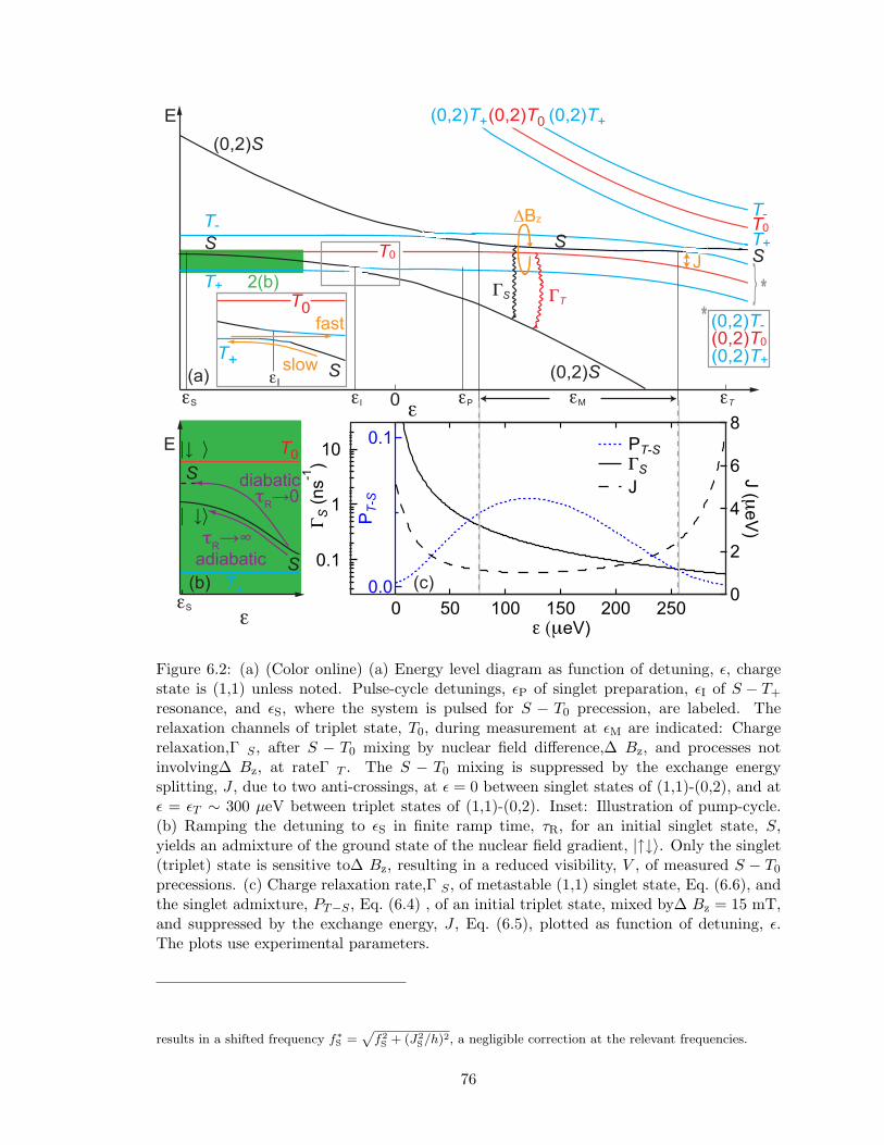
0.1
1
10
S (n
s-1)
250200150100500 (µeV)
0.1
0.0
P T-S
8
6
4
2
0
J (µeV)
PT-S S J
E
T-
0
(0,2)S
(0,2)S
T+
T0
S MI P T
SSBz
TS
J
(0,2)T0 (0,2)T+(0,2)T+
T-T+T0
S
(0,2)T0(0,2)T+
(0,2)T-
**
(a)
(c)
E
T+S
T0
S
diabatic
adiabatic
SR
R
2(b)
(b)
T+I
T0
S
fast
slow
Figure 6.2: (a) (Color online) (a) Energy level diagram as function of detuning, , chargestate is (1,1) unless noted. Pulse-cycle detunings, P of singlet preparation, I of S − T+
resonance, and S, where the system is pulsed for S − T0 precession, are labeled. Therelaxation channels of triplet state, T0, during measurement at M are indicated: Chargerelaxation,Γ S , after S − T0 mixing by nuclear field difference,∆ Bz, and processes notinvolving∆ Bz, at rateΓ T . The S − T0 mixing is suppressed by the exchange energysplitting, J , due to two anti-crossings, at = 0 between singlet states of (1,1)-(0,2), and at = T ∼ 300 µeV between triplet states of (1,1)-(0,2). Inset: Illustration of pump-cycle.(b) Ramping the detuning to S in finite ramp time, τR, for an initial singlet state, S,yields an admixture of the ground state of the nuclear field gradient, |↑↓. Only the singlet(triplet) state is sensitive to∆ Bz, resulting in a reduced visibility, V , of measured S − T0
precessions. (c) Charge relaxation rate,Γ S , of metastable (1,1) singlet state, Eq. (6.6), andthe singlet admixture, PT−S , Eq. (6.4) , of an initial triplet state, mixed by∆ Bz = 15 mT,and suppressed by the exchange energy, J , Eq. (6.5), plotted as function of detuning, .The plots use experimental parameters.
results in a shifted frequency f∗S =p
f2S + (J2
S/h)2, a negligible correction at the relevant frequencies.
76
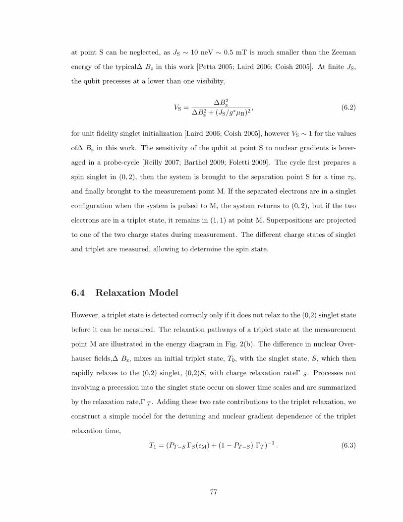
at point S can be neglected, as JS ∼ 10 neV ∼ 0.5 mT is much smaller than the Zeeman
energy of the typical∆ Bz in this work [Petta 2005; Laird 2006; Coish 2005]. At finite JS,
the qubit precesses at a lower than one visibility,
VS =∆B2
z
∆B2z + (JS/g∗µB)2
, (6.2)
for unit fidelity singlet initialization [Laird 2006; Coish 2005], however VS ∼ 1 for the values
of∆ Bz in this work. The sensitivity of the qubit at point S to nuclear gradients is lever-
aged in a probe-cycle [Reilly 2007; Barthel 2009; Foletti 2009]. The cycle first prepares a
spin singlet in (0, 2), then the system is brought to the separation point S for a time τS,
and finally brought to the measurement point M. If the separated electrons are in a singlet
configuration when the system is pulsed to M, the system returns to (0, 2), but if the two
electrons are in a triplet state, it remains in (1, 1) at point M. Superpositions are projected
to one of the two charge states during measurement. The different charge states of singlet
and triplet are measured, allowing to determine the spin state.
6.4 Relaxation Model
However, a triplet state is detected correctly only if it does not relax to the (0,2) singlet state
before it can be measured. The relaxation pathways of a triplet state at the measurement
point M are illustrated in the energy diagram in Fig. 2(b). The difference in nuclear Over-
hauser fields,∆ Bz, mixes an initial triplet state, T0, with the singlet state, S, which then
rapidly relaxes to the (0,2) singlet, (0,2)S, with charge relaxation rateΓ S . Processes not
involving a precession into the singlet state occur on slower time scales and are summarized
by the relaxation rate,Γ T . Adding these two rate contributions to the triplet relaxation, we
construct a simple model for the detuning and nuclear gradient dependence of the triplet
relaxation time,
T1 = (PT−S ΓS(M) + (1− PT−S) ΓT )−1 . (6.3)
77
At the measurement point, M, an exchange energy splitting, J , between the singlet and
triplet state suppresses the S − T0 mixing, such that only a small fraction, PT−S , of the
initial triplet population is in a singlet state at a given time. At large exchange, and
small relaxation rates, the evolution at M can be described by the eigenstates of the co-
herent evolution of the qubit in∆ Bz and J , with a triplet-like eigenstate and a singlet-like
eigenstate [Taylor PRB 2007]. For an initial triplet state, the population of the singlet-like
eigenstate is negligible and the evolution reduces to the relaxation of the triplet-like eigen-
state. Following the analysis in Ref. [Taylor PRB 2007], PT−S is calculated from the singlet
projection of the triplet-like eigenstate
PT−S =12
1− J(M)
∆B2z + J(M)2
. (6.4)
The exchange, J , is function of the energy detuning, M , of the point M, and is due to two
charge state anti-crossings. The first anti-crossing is between the singlet states of the (0,2)
and (1,1) charge configuration at = 0; the second anti-crossing, at = T , is between the
m = 0 triplet states of the (0,2) and (1,1) charge configuration. The exchange at > 0
cannot be measured directly and is approximated with the expression
J =t2S
+
4 t2S + 2− t2T
(− T )−
4 t2T + (− T )2(6.5)
from Ref. [Taylor PRB 2007], where tS is the tunnel coupling for singlet states, and tT is the
tunnel coupling for triplet states. Equation (6.5) neglects the change in tunnel couplings
due to changes in via gate voltage pulses, which is believed to give deviations from this
functional form [Laird 2006].
The detuning dependence of the charge relaxation rate,Γ S , has been discussed and
experimentally studied in Ref. [Fujisawa 1998]. There, a decrease in relaxation rate with
increased detuning, roughly faster than −1 but slower than −2, was found and compared
to expected power laws for different dissipation mechanisms. For piezoelectric interaction
with 3D (2D) phonons, a power law,Γ S ∝ −1 (−2), is expected [Fujisawa 1998]. As an
78
approximate description of the -dependence of the charge relaxation we use
ΓS = α−1 + β−2. (6.6)
The singlet charge relaxation rate,Γ S , Eq. (6.6), the exchange, J , Eq. (6.5), and the singlet
admixture, PT−S , of an initial triplet state, Eq. (6.4), are shown as function of detuning, ,
in Fig. 6.2(c). Experimental parameters, discussed in section 6.5, are used in the plots.
We now discuss the effects of finite pulse rise times. In order to perform S−T0 precession
experiments, or for qubit initialization in quantum information processing, a singlet state,
S, typically is initialized by electron separation from an (0, 2)S singlet state, as discussed
above. Figure 6.2(b) shows a close-up of the level diagram at large negative detuning, S,
where S and T0 are nearly degenerate and split by residual exchange, JS, smaller than the
typical Zeeman splitting between the two eigenstates in the nuclear Overhauser fields, |↑↓
and |↓↑. The arrows in |↑↓ indicate the electron spin in the left (right) dot being parallel
(anti-parallel) to the quantization axis,∆ Bz > 0 is assumed without loss of generality.
In that notation the triplet / singlet state is T/S = (|↑↓ ± |↓↑)/√
2 and in the limit,
JS/∆Bz → 0, the nuclear field eigenstates become the eigenstates of the total Hamiltonian,
as illustrated in Figure 6.2(b). A singlet, separated infinitely slowly with a ramp time,
τR →∞, is adiabatically loaded into the ground state of the nuclear field, |↑↓ [Petta 2005;
Taylor PRB 2007]. In the limit of instantaneous separation, with a ramp time, τR → 0, a
pure singlet state is initialized. For finite ramp- or rise-times, a singlet is initialized with
a smaller than one fidelity, with some admixture of the nuclear eigenstates. Similarly, the
recombination of the two electrons into one dot, after evolution in point S, only maps the
S, T0 state onto the (0,2), (1,1) charge state with unity fidelity for an instantaneous change
of detuning, . For a finite ramp time, the visibility of singlet and triplet is reduced due
to admixture of the nuclear eigenstates, analogous to the separation. In the final part of
this paper, the influence of ramp- and rise-time on initialization fidelity, FI, incorporating
visibility reduction due to the finite duration of both separation and recombination, is
investigated.
79
6.5 Time evolution of nuclear Gradient and S − T0 Visibility
To study the nuclear gradients built by the electron-nuclear spin flips, pump-probe ex-
periments are performed. The nuclear state is prepared by a pump-cycle, with a ∼ 4 MHz
repetition rate, ramping through ∼ 10 µeV around I in 100 ns. The pump-cycle is repeated
∼ 240 million times over 60 s. The waveform generator then immediately performs a se-
quence of probe-cycles, with varying τS, to extract the nuclear field difference from S − T0
precessions. The singlet measurement probability, PS , is determined from single-shot mea-
surements, following the procedure described in Ref. [Barthel 2009]. After preparation in
(0, 2)S at P, the probe-cycle cycle separates the singlet to point S, see Figs. 6.1(b), 6.2(a),
without nominal ramp time, τR = 0. The system is held at detuning, S ∼ −700 µeV, for
the separation time, τS, and is then brought back to the measurement point M, where the
charge signal, vrf , is recorded over the total measurement time, τmaxM ∼ 10µs. The charge
signal, vrf , is then integrated over ∼ 300 ns, yielding single-shot measurement outcomes, Vrf ,
which are identified as singlet or triplet outcomes by comparison to a threshold voltage, as
discussed in Ref. [Barthel 2009]. For each separation time, τS, 100 single-shot measurements
are performed, and the singlet measurement probability, PS , is calculated as the percentage
of singlet outcomes. Figure 6.3(a) shows PS as function of τS and time,∆ t, after the pump-
cycle. The separation time, τS, is stepped from 1 ns to 100 ns in 80 steps, for a total of
8000 single-shot measurements before the data is saved and processed. Sets of 8000 cycles,
corresponding to a column in Fig. 6.3(a), are acquired every second, and are shown for two
values of∆ t in Fig. 6.3(b). Measurements immediately after the pump-cycle,∆ t 50 s,
show an almost unity singlet measurement probability, PS , while after longer times,∆ t,
high frequency, low visibility oscillations become visible. At long times,∆ t 300s, close
to unity visibility S − T0 precessions with frequencies corresponding to equilibrium nuclear
field differences,∆ Bz, are observed. Fourier transforms (FFT) of PS are calculated and the
normalized Fourier amplitude AFFT is plotted as function of frequency, fS, and time after
pumping,∆ t, in Fig. 6.3(c). The Fourier transforms have clear maxima, as illustrated by
two vertical cuts through the data in Fig. 6.3(c) at∆ t = 150 s and∆ t = 300 s, shown in
Fig. 6.3(d). The frequency with maximum FFT component is correlated for two adjacent
80
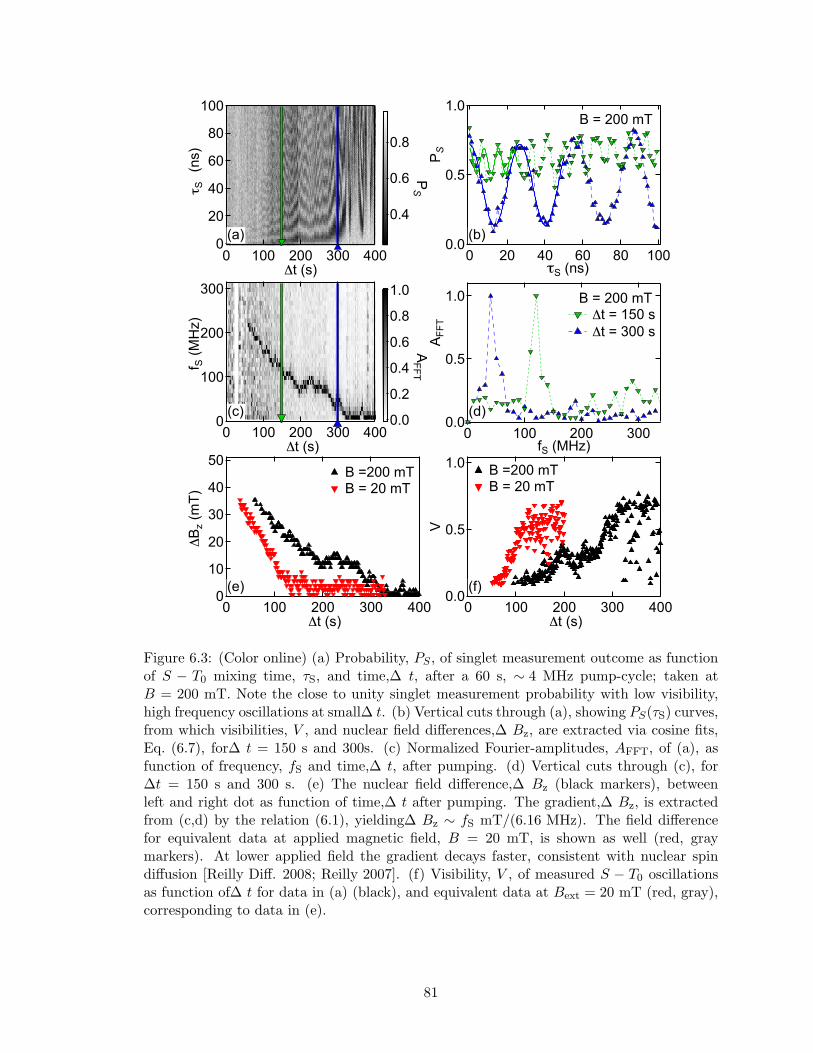
100
80
60
40
20
0
S
(n
s)
4003002001000t (s)
0.8
0.6
0.4
PS
1.0
0.5
0.0
P S
100806040200 S (ns)
4003002001000 t (s)
300
200
100
0
f S (M
Hz)
1.0
0.8
0.6
0.4
0.2
0.0
AFFT
4003002001000 t (s)
50
40
30
20
10
0
Bz (
mT
)
B =200 mTB = 20 mT
1.0
0.5
0.0A F
FT3002001000
fS (MHz)
B = 200 mT t = 150 s t = 300 s
1.0
0.5
0.0
V
4003002001000 t (s)
B =200 mTB = 20 mT
(a)
(c)
(e)
(b)
(d)
(f)
B = 200 mT
Figure 6.3: (Color online) (a) Probability, PS , of singlet measurement outcome as functionof S − T0 mixing time, τS, and time,∆ t, after a 60 s, ∼ 4 MHz pump-cycle; taken atB = 200 mT. Note the close to unity singlet measurement probability with low visibility,high frequency oscillations at small∆ t. (b) Vertical cuts through (a), showing PS(τS) curves,from which visibilities, V , and nuclear field differences,∆ Bz, are extracted via cosine fits,Eq. (6.7), for∆ t = 150 s and 300s. (c) Normalized Fourier-amplitudes, AFFT, of (a), asfunction of frequency, fS and time,∆ t, after pumping. (d) Vertical cuts through (c), for∆t = 150 s and 300 s. (e) The nuclear field difference,∆ Bz (black markers), betweenleft and right dot as function of time,∆ t after pumping. The gradient,∆ Bz, is extractedfrom (c,d) by the relation (6.1), yielding∆ Bz ∼ fS mT/(6.16 MHz). The field differencefor equivalent data at applied magnetic field, B = 20 mT, is shown as well (red, graymarkers). At lower applied field the gradient decays faster, consistent with nuclear spindiffusion [Reilly Diff. 2008; Reilly 2007]. (f) Visibility, V , of measured S − T0 oscillationsas function of∆ t for data in (a) (black), and equivalent data at Bext = 20 mT (red, gray),corresponding to data in (e).
81
columns and decreases with time after pumping,∆ t, as expected for a decaying nuclear
field gradient,∆ Bz. The values of nuclear field difference,∆ Bz, from FFT peak positions
are used as starting points for fits of
PS = P0 + 1/2 V cos (2πfSτS) (6.7)
to the time domain precession data, as shown in Fig. 6.3(b), with frequency, fS, given by
Eq. (6.1). The nuclear field differences,∆ Bz, extracted from the fits of Eq. (6.1) agree with
the values from Fourier transform peak positions within one FFT bin size (∼ 1 mT). For
the cut at∆ t ∼ 150 s the visibility is V = 0.2, and the extracted nuclear field difference
is∆ Bz ∼ 20 mT, while for the cut at∆ t ∼ 300 s, V = 0.6, and∆ Bz ∼ 6 mT 3. Fig-
ure 6.3(e) shows the nuclear field difference,∆ Bz, corresponding to the frequency, fS, of
maximum Fourier amplitude, AFFT, in Fig. 6.3(c), according to Eq. (6.1). For an iden-
tical pump-probe experiment, performed at applied field, B = 20 mT, the nuclear field
difference,∆ Bz, from FFT peak positions is shown as well. Note that the decay of the
field difference with time,∆ t, is faster for the 20 mT data, consistent with nuclear spin
diffusion [Reilly 2007; Reilly Diff. 2008]. Visibilities, V , extracted from fits, Eq. (6.7), are
shown as function of∆ t in Fig. 6.3(f) .
6.6 Triplet Relaxation Time as Function of magnetic Field
Difference
To investigate the dependence of the visibility on the magnetic field difference and the mech-
anism reducing the visibility, pump-probe measurements are performed for nine values of
measurement point detuning, M, after a 60 s, 4 MHz pump-cycle. Measured visibilities, V ,
are shown in Fig. 6.4(a) as function of the simultaneously measured nuclear field difference,
∆Bz, for three of the nine values of M. The visibility sharply decreases with increasing
3Other parameters are, P0 = 0.6 for∆ t = 150s, and P0 = 0.4 for∆ t = 150s.
82
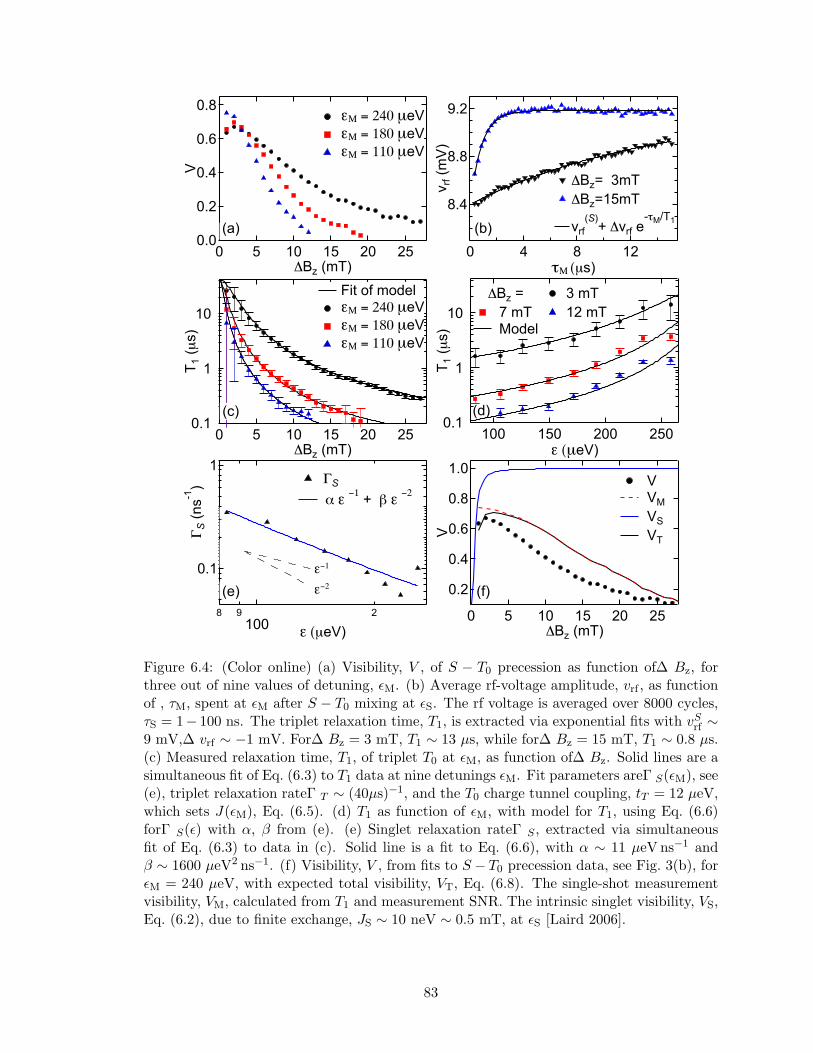
0.8
0.6
0.4
0.2
0.0
V
2520151050Bz (mT)
= 240 µeV
= 180 µeV
= 110 µeV
9.2
8.8
8.4
v rf (
mV
)
12840 (µs)
Bz= 3mTBz=15mT
vrf(S)
+ vrf e- M/T1
0.1
1
10
T1 (
µs)
2520151050Bz (mT)
Fit of model = 240 µeV
= 180 µeV
= 110 µeV
0.1
1
10
T1 (
µs)
250200150100 (µeV)
Bz = 3 mT
7 mT 12 mT Model
0.1
1
S (
ns
-1)
8 9
1002
(µeV)
S
1 +
2
1.0
0.8
0.6
0.4
0.2
V
2520151050Bz (mT)
V VM
VS
VT
(a)
(c)
(e)
(b)
(d)
(f)
Figure 6.4: (Color online) (a) Visibility, V , of S − T0 precession as function of∆ Bz, forthree out of nine values of detuning, M. (b) Average rf-voltage amplitude, vrf , as functionof , τM, spent at M after S − T0 mixing at S. The rf voltage is averaged over 8000 cycles,τS = 1− 100 ns. The triplet relaxation time, T1, is extracted via exponential fits with vS
rf ∼9 mV,∆ vrf ∼ −1 mV. For∆ Bz = 3 mT, T1 ∼ 13 µs, while for∆ Bz = 15 mT, T1 ∼ 0.8 µs.(c) Measured relaxation time, T1, of triplet T0 at M, as function of∆ Bz. Solid lines are asimultaneous fit of Eq. (6.3) to T1 data at nine detunings M. Fit parameters areΓ S(M), see(e), triplet relaxation rateΓ T ∼ (40µs)−1, and the T0 charge tunnel coupling, tT = 12 µeV,which sets J(M), Eq. (6.5). (d) T1 as function of M, with model for T1, using Eq. (6.6)forΓ S() with α, β from (e). (e) Singlet relaxation rateΓ S , extracted via simultaneousfit of Eq. (6.3) to data in (c). Solid line is a fit to Eq. (6.6), with α ∼ 11 µeV ns−1 andβ ∼ 1600 µeV2 ns−1. (f) Visibility, V , from fits to S − T0 precession data, see Fig. 3(b), forM = 240 µeV, with expected total visibility, VT, Eq. (6.8). The single-shot measurementvisibility, VM, calculated from T1 and measurement SNR. The intrinsic singlet visibility, VS,Eq. (6.2), due to finite exchange, JS ∼ 10 neV ∼ 0.5 mT, at S [Laird 2006].
83
magnetic field differences, while the curves for smaller detuning, M, fall off with∆ Bz more
rapidly. The total S−T0 precession visibility, VT, is reduced from unity due to two expected
mechanisms,
VT = VM VS, (6.8)
where the measurement visibility, VM , captures the imperfect fidelity of the single-shot
measurement, as discussed in Ref. [Barthel 2009]. The intrinsic visibility, VS, due to finite
exchange, JS, at the point S, Eq. (6.2), is VS ∼ 1 for all but the smallest nuclear field differ-
ences,∆ Bz 1 mT. The measurement visibility, VM, is calculated from the experimental
parameters following the analysis in Ref. [Barthel 2009], and depends on the triplet relax-
ation time, T1, at the measurement point. In order to determine the dependence of T1 on
∆Bz, the relaxation of a triplet state at the measurement point is monitored via the charge
signal, vrf , which is recorded with 100 ns time resolution over total time, τmaxM = 4 µs. After
200 s, the total time spent at M is increased from 4 µs to 15 µs, while the time resolution
is changed from 100 ns to 250 ns, in order to measure short and long relaxation times, T1,
optimally using oscilloscope memory. Figure 6.4(b) shows the rf voltage signal, vrf , averaged
over 8000 probe-cycles, with τS ranging from 1 to 100 ns, as function of the time, τM, spent
at the measurement point M. The voltage, vrf , decays from v(S)rf + ∆vrf , corresponding to
an equal mixture of charge states (0,2) and (1,1), to v(S)rf , corresponding to the (0,2) charge
state. The exponential fit yields a value of T1 ∼ 13 µs for data taken at∆ Bz = 3 mT and
a significantly smaller value of T1 ∼ 0.8 µs for the data taken at∆ Bz = 15 mT.
The triplet relaxation time, T1, is shown as function of nuclear field gradient,∆ Bz, in
Fig. 6.4(c) for three different values of measurement point detuning, M. Like the visibility,
the triplet relaxation time, T1, decreases sharply with increasing∆ Bz, and with decreasing
M as shown in Fig. 6.4(d) for three different values of∆ Bz. To test whether the observed
nuclear field dependence agrees with the model, a fit of Eq. (6.3) is performed simultaneously
for nine values of M, with ∆Bz as independent variable. The exchange, J(M), at point M
is set by Eq. (6.5), and contains one fit parameter, the triplet tunnel coupling, tT ∼ 12 µeV.
Assuming Eq. 6.5, the singlet tunnel coupling, tS ∼ 10 µeV, is estimated from the detuning,
84
I, of the S - T+ resonance footnoteAt I, the exchange energy, JS, is equal to the Zeeman en-
ergy of T+. Comparison with JS = t2S/(I−
4t2S + 2I ), from Ref. [Taylor PRB 2007], yields
an estimate of tS .. The energy detuning, T ∼ 300 µeV, of the triplet charge transition is
determined from dc transport measurements [Johnson PRB 2005; Van der Wiel 2003]. The
fit, together with the measured parameters, yields the dependence of exchange energy, J(),
shown in Fig. 6.2(c). The bare triplet relaxation rate,Γ T ∼ (40 µs)−1, is fitted to be equal
for all detunings, an estimation that is justified by the weak dependence of Eq. (6.3) onΓ T
for∆ Bz > 1 mT and because measured values of T1 agree with each other within the errors
at small∆ Bz. For the singlet charge relaxation rate,Γ S(M), one fit parameter is used for
each detuning, M, yielding the values shown in Fig. 6.4(e). The rate,Γ S , decreases with in-
creasing detuning, and a fit of Eq. (6.6), yielding α ∼ 11 µeV ns−1 and β ∼ 1600 µeV2 ns−1,
shows reasonable agreement with the data. At M ∼ 150 µeV, the contributions from 2D
and 3D phonons are about equal. The charge relaxation rates are consistent with the val-
ues measured in Ref. [Fujisawa 1998], when taking into account the difference in tunnel
couplings, tS . Deviations from the form (6.6) are expected, e.g. due to resonances from
finite lengths in the phonon environment [Fujisawa 1998]. Figure 6.4(d) shows the model,
Eq. (6.3), withΓ S() from Eq. (6.6), using α and β from the fit in Fig. 6.4(e). Note that the
extracted values of α and β are rough estimates, as the functional form of J(M), Eq. (6.5), is
only approximate. The detuning dependence ofΓ S, assuming Eq. 6.6 and using the obtained
fit parameters α and β, is shown in Fig. 6.2(c). SinceΓ S ∝ t2S [Fujisawa 1998], and roughly
J ∝ t2S (tT increases with tS), the first and dominant term in Eq. (6.3) becomes ∝ ∆B2z/t2S
for∆ Bz < J . Contrary to intuition, a more transparent tunnel barrier yields longer triplet
relaxation times, which is beneficial for quantum information processing, where large tunnel
couplings enable fast operations [Petta 2005; Foletti 2009].
85
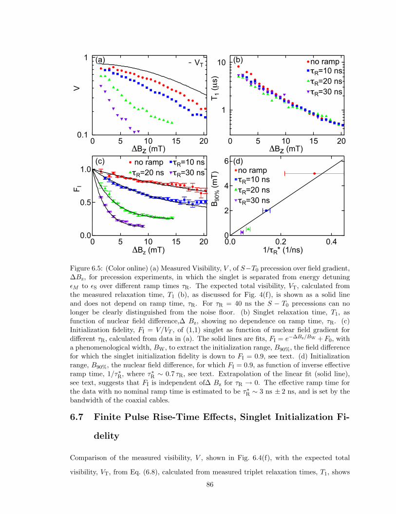
(a) (b)
(c) (d)
Figure 6.5: (Color online) (a) Measured Visibility, V , of S−T0 precession over field gradient,∆Bz, for precession experiments, in which the singlet is separated from energy detuningM to S over different ramp times τR. The expected total visibility, VT, calculated fromthe measured relaxation time, T1 (b), as discussed for Fig. 4(f), is shown as a solid lineand does not depend on ramp time, τR. For τR = 40 ns the S − T0 precessions can nolonger be clearly distinguished from the noise floor. (b) Singlet relaxation time, T1, asfunction of nuclear field difference,∆ Bz, showing no dependence on ramp time, τR. (c)Initialization fidelity, FI = V/VT , of (1,1) singlet as function of nuclear field gradient fordifferent τR, calculated from data in (a). The solid lines are fits, FI = e−∆Bz/BW + F0, witha phenomenological width, BW, to extract the initialization range, B90%, the field differencefor which the singlet initialization fidelity is down to FI = 0.9, see text. (d) Initializationrange, B90%, the nuclear field difference, for which FI = 0.9, as function of inverse effectiveramp time, 1/τ∗R, where τ∗R ∼ 0.7 τR, see text. Extrapolation of the linear fit (solid line),see text, suggests that FI is independent of∆ Bz for τR → 0. The effective ramp time forthe data with no nominal ramp time is estimated to be τ∗R ∼ 3 ns ± 2 ns, and is set by thebandwidth of the coaxial cables.
6.7 Finite Pulse Rise-Time Effects, Singlet Initialization Fi-
delity
Comparison of the measured visibility, V , shown in Fig. 6.4(f), with the expected total
visibility, VT, from Eq. (6.8), calculated from measured triplet relaxation times, T1, shows
86
qualitative agreement. The theory curve, VT, slightly overestimates the measured visibility
except for low values of∆ Bz. We speculate that this deviation is due to imperfect initial-
ization (separation) and recombination of a singlet state, reducing the measured visibility,
V = VTFI. (6.9)
The initialization fidelity, FI, captures the reduction in visibility due to an admixture of
the nuclear ground state because the separation of the singlet is not completely diabatic,
see Fig. 6.2(b), and the analogous reduction because the recombination of the two electrons
into one dot is not diabatic either. To test this hypothesis, pump-probe experiments with
an intentional ramp time, τR, are performed. As discussed above, a 4 MHz pump-cycle is
executed for 60 s. During the subsequent probe-cycles, a prepared singlet is separated from
the (0,2) charge state at M to the (1,1) charge state at point S over the ramp time, τR.
After evolution in the nuclear field difference,∆ Bz, the system is ramped back to the point
M, over the same ramp time. The singlet measurement probability, PS , is measured for the
same parameters as the data in Fig. 6.4, and the triplet relaxation time, T1, is measured
as discussed for Fig. 6.4(b). As a control, a pump-probe experiment without nominal
ramp is performed under the same conditions. The measured visibilities, V , are shown in
Fig. 6.5(a), together with the expected visibility, VT, calculated from the measured T1, using
Eq. (6.8) and following Ref. [Barthel 2009]. The relaxation time, T1, does not depend on
τR as shown in Fig. 6.5(b). The initialization fidelity, FI, shown in Fig. 6.5(c), is calculated
as the ratio, FI = V/VT, of measured and expected visibility. For larger ramp times, FI
falls off with∆ Bz more rapidly. Due to the finite rise time of the pulses, the data with
no nominal ramp time has an estimated effective ramp time, τ∗R ∼ 3 ns, and a fidelity,
FI < 1, at finite nuclear field differences. For the data with nominal ramp times, the
effective ramp time, τ∗R ∼ 0.7 τR, is estimated from the fraction of the ramp that is spent
in (1,1) at exchange energies, comparable to the Zeeman energy corresponding to∆ Bz.
To characterize the decline in fidelity with∆ Bz, we define the initialization range, B90%,
the maximum nuclear field gradient for which the fidelity, FI 0.9. A phenomenological
exponential curve is fitted to the fidelities shown in Fig. 6.5(c) to extract B90%, which
87
increases with increasing effective ramp rate, 1/τ∗R, as shown in Fig. 6.5(d)4. The increase
in B90% is approximately linear in 1/τ∗R. A linear fit, shown in Fig. 6.5(d) agrees reasonably
well with the data. This suggests that the smaller than unity fidelity for the probe-cycle
without nominal ramp time is due to the finite pulse rise time. For higher bandwidth
coaxial cables, a larger singlet initialization fidelity may be obtained, even in the presence
of magnetic field gradients. Moreover the S − T0 precession data at finite ramp-times
constitutes a weak measurement of the nuclear field gradient,∆ Bz, with the initialization
fidelity, FI, as coupling parameter [Aharonov 1988; Romito 2008].
6.8 Magnetic Field Dependence, alternative Interpretation
of Unity Singlet Return Probability after nuclear Pump-
ing
Pump probe experiments have been performed in six cool-downs of four devices for three
different magnetic field directions, along all three crystal axes, indicated in Fig. 6.1(a), and
at a wide range of magnetic field magnitudes between 10 mT and 2 T. For data shown in
this paper, B is applied along the direction given in Fig. 6.1(a). At all fields, the same
qualitative phenomenology, i.e. a nuclear field gradient and an average nuclear polariza-
tion of comparable magnitude, have been observed, while at no field value a suppression
of nuclear field fluctuations was found. We speculate that the phenomenology reported in
Ref. [Reilly 2008] was the result of a nuclear field gradient,∆ Bz, much larger than the equi-
librium field fluctuations, suppressing the measurement visibility. Drifts of the measurement
point M result in changes of sensor conductance and measurement visibility, that mimic a
reduction of PS for long separation times, as observed and interpreted as a T ∗2 envelope in
Ref. [Reilly 2008]. The fast, low-visibility precession would not be distinguishable from a
4The saturation values, F0, used in fits in Fig. 6.5(c), may be spurious since visibilities are approachingthe noise levels. Initialization range, B90%, is used to obtain a width insensitive to errors in low FI valuesat high∆ Bz. For no ramp, F0 ∼ 0.3, BW ∼ 31 mT; for τR = 10 ns, F0 ∼ 0.3, BW ∼ 12 mT; for τR = 20 ns,F0 ∼ 0.2, BW ∼ 4 mT; for τR = 30 ns, F0 ∼ 0.1, BW ∼ 2 mT. In Fig. 6.5(d), the slope of the linear fit is∼ 14 mTns.
88
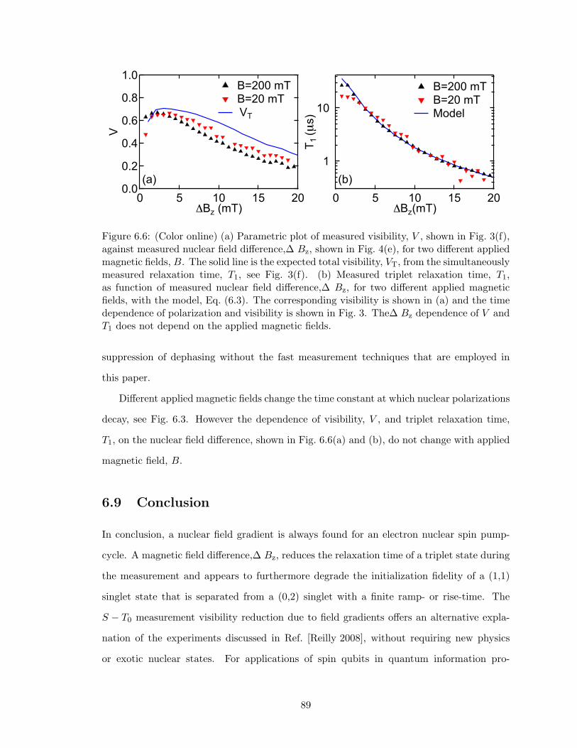
1.0
0.8
0.6
0.4
0.2
0.0
V
20151050Bz (mT)
B=200 mT B=20 mT VT
1
10
T1 (µ
s)
20151050Bz(mT)
B=200 mT B=20 mT Model
(a) (b)
Figure 6.6: (Color online) (a) Parametric plot of measured visibility, V , shown in Fig. 3(f),against measured nuclear field difference,∆ Bz, shown in Fig. 4(e), for two different appliedmagnetic fields, B. The solid line is the expected total visibility, VT, from the simultaneouslymeasured relaxation time, T1, see Fig. 3(f). (b) Measured triplet relaxation time, T1,as function of measured nuclear field difference,∆ Bz, for two different applied magneticfields, with the model, Eq. (6.3). The corresponding visibility is shown in (a) and the timedependence of polarization and visibility is shown in Fig. 3. The∆ Bz dependence of V andT1 does not depend on the applied magnetic fields.
suppression of dephasing without the fast measurement techniques that are employed in
this paper.
Different applied magnetic fields change the time constant at which nuclear polarizations
decay, see Fig. 6.3. However the dependence of visibility, V , and triplet relaxation time,
T1, on the nuclear field difference, shown in Fig. 6.6(a) and (b), do not change with applied
magnetic field, B.
6.9 Conclusion
In conclusion, a nuclear field gradient is always found for an electron nuclear spin pump-
cycle. A magnetic field difference,∆ Bz, reduces the relaxation time of a triplet state during
the measurement and appears to furthermore degrade the initialization fidelity of a (1,1)
singlet state that is separated from a (0,2) singlet with a finite ramp- or rise-time. The
S − T0 measurement visibility reduction due to field gradients offers an alternative expla-
nation of the experiments discussed in Ref. [Reilly 2008], without requiring new physics
or exotic nuclear states. For applications of spin qubits in quantum information pro-
89
cessing, where magnetic field gradients are promising tools in the realization of quantum
gates [Foletti 2009; Pioro-Ladriere 2007], it is desirable to engineer the exchange profile to
allow long triplet lifetimes, e.g. by having an (0,2) singlet-triplet splitting slightly larger
than the measurement detuning. In the presence of a magnetic field difference, the device
should be tuned to a large inter-dot tunnel coupling with a measurement point chosen at
large detuning, where exchange protects the triplet and the charge relaxation rate is small.
To mitigate errors from finite pulse rise times, an initialization of the qubit via an adiabatic
initialization of |↑↓, followed by a π/2 pulse, may be preferable over the diabatic initializa-
tion used here and in Refs. [Petta 2005; Foletti 2009; Reilly 2007]. We would like to point
out that the results of this paper do not imply a short relaxation time of the qubit while it
is operated in the (1, 1) state, where T1 is much longer and expected to be independent of
magnetic field gradient [Amasha 2008].
Acknowledgments
We acknowledge funding from ARO/iARPA, the Department of Defense. This work was
performed in part at the Center for Nanoscale Systems (CNS), a member of the National
Nanotechnology Infrastructure Network (NNIN), which is supported by the National Science
Foundation under NSF award no. ECS-0335765. We thank D.J. Reilly, J.M. Taylor and S.
Foletti for useful discussion.
90
Chapter 7
Dynamic Decoupling andinterlaced Operation of aSinglet-Triplet Qubit
C. Barthel1,3 J. Medford1,3 C. M. Marcus1 M. P. Hanson2 A. C. Gossard2 1Department of
Physics, Harvard University, Cambridge, Massachusetts 02138, USA
2Materials Department, University of California, Santa Barbara, California 93106, USA
3 These authors contributed equally to this work.
We demonstrate interlacing of Carr Purcell (CP) spin echo sequences with coherent
operations on a singlet-triplet qubit, formed by the spins of a two-electron GaAs double
quantum dot. Qubit operations are performed using exchange and the Overhauser nuclear
field difference between the two dots. The initial and final states of these operations are
preserved from decoherence over tens of microseconds. Different decoupling sequences,
Hahn echo (HE), CP, Concatenated dynamical decoupling (CDD) and Uhrig dynamical
decoupling (UDD) are compared in their effectiveness to preserve an initialized singlet state.
We find that for our system and setup the coherence time achieved employing a CP sequence
is as high as for a CDD sequence and significantly higher than the time achieved with a
UDD sequence, for similar numbers of π-pulses. Coherence times 100 µs are observed for
a CP spin echo sequence 1.
1This chapter is adapted from a manuscript in preparation for submission [Barthel T2 2010].
91
7.1 Introduction
The singlet-triplet basis of a pair of electron spins in two coupled quantum dots has been
suggested as a logical qubit for quantum information processing [Loss 1998; Levy 2002].
The qubit is inherently protected against collective dephasing [Levy 2002], and more im-
portantly allows for all-electrical sub-nanosecond operations, using the exchange energy
between singlet and triplet states to perform rotations around one of the qubit blochspere
axes [Petta 2005]. Qubit rotations around a second independent axis, needed for univer-
sal qubit control, can be induced by a magnetic field difference between the two quantum
dots, for example from a micro magnet on top of the double dot [Pioro-Ladriere 2007],
and have recently been realized via a gradient in the nuclear polarization of the host
material [Foletti 2009]. Fast measurement of a qubit state has been demonstrated for
two-electron spin states [Meunier 2006; Barthel 2009], and also for single electron spin
states [Elzerman 2004; Amasha 2008]. Aside from being a useful tool to manipulate the
qubit, the Overhauser fields from the nuclei also are the major source of qubit dephas-
ing [Petta 2005]. The fluctuations of nuclear fields have been shown to be slow [Reilly 2007],
and a Hahn spin echo pulse sequence has been used to extend the coherence time of a singlet
to up to ∼ 30 µs [Hahn 1950; Petta 2005; Bluhm T2 2010]. Carr Purcell (CP) spin echo
pulse sequences have been used to extend qubit coherence times up to ∼ 200 µs [Carr 1954;
Meiboom 1958; Bluhm T2 2010]. Theoretical work suggests that, under the assumptions of
certain dephasing power spectra, spin echo sequences more complex than CP could further
increase coherence times [Witzel CDD 2007; Uhrig 2007].
In this rapid communication we demonstrate the protection of a generalized singlet-
triplet superposition from decoherence by interlacing qubit rotations about two different
Bloch sphere axes into two CP spin echo pulse sequences. For nuclear Overhauser field
driven rotations around the x-axis of the qubit Bloch sphere, and exchange energy driven
rotations around the z-axis of the Bloch sphere, oscillations in singlet return probability
are preserved up to 60 µs, comparable to singlet coherence times. Finally, we compare the
coherence times of a singlet, protected by a single Hahn echo (HE), a CP echo sequence
with 16 π-pulses [Carr 1954; Meiboom 1958; Bluhm T2 2010], a 5th order Concatenated
92
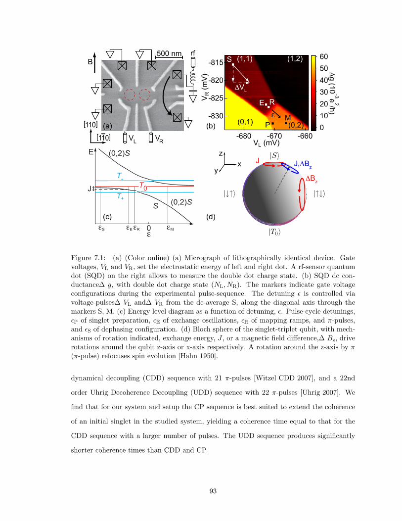
-830
-825
-820
-815
VR (
mV
)
-680 -670 -660VL (mV)
60
50
40
30
20
10
0
g (1
0-3e
2/h)
(0,1)
(1,2)(1,1)
(0,2)M
R
S
P
VL
E
0
E (0,2)S
(0,2)S
T-
T+
S M
T0
S
E
J
R
(b)
(c) (d)
VL VR
500 nm rfB
[110]
[110](a)
J
Bz
zx
yJ, Bz
Figure 7.1: (a) (Color online) (a) Micrograph of lithographically identical device. Gatevoltages, VL and VR, set the electrostatic energy of left and right dot. A rf-sensor quantumdot (SQD) on the right allows to measure the double dot charge state. (b) SQD dc con-ductance∆ g, with double dot charge state (NL, NR). The markers indicate gate voltageconfigurations during the experimental pulse-sequence. The detuning is controlled viavoltage-pulses∆ VL and∆ VR from the dc-average S, along the diagonal axis through themarkers S, M. (c) Energy level diagram as a function of detuning, . Pulse-cycle detunings,P of singlet preparation, E of exchange oscillations, R of mapping ramps, and π-pulses,and S of dephasing configuration. (d) Bloch sphere of the singlet-triplet qubit, with mech-anisms of rotation indicated, exchange energy, J , or a magnetic field difference,∆ Bz, driverotations around the qubit z-axis or x-axis respectively. A rotation around the z-axis by π(π-pulse) refocuses spin evolution [Hahn 1950].
dynamical decoupling (CDD) sequence with 21 π-pulses [Witzel CDD 2007], and a 22nd
order Uhrig Decoherence Decoupling (UDD) sequence with 22 π-pulses [Uhrig 2007]. We
find that for our system and setup the CP sequence is best suited to extend the coherence
of an initial singlet in the studied system, yielding a coherence time equal to that for the
CDD sequence with a larger number of pulses. The UDD sequence produces significantly
shorter coherence times than CDD and CP.
93
7.2 System and Setup
The double quantum dot and sensor are defined by Ti/Au depletion gates on a GaAs /
Al0.3Ga0.7As heterostructure with a two-dimensional electron gas (density 2 × 10¹⁵ m−2,
mobility 20 m2/Vs) 100 nm below the surface. An in-plane magnetic field, B = 750 mT, is
applied perpendicular to the dot connection axis, as indicated in Fig. 7.1(a). Measurements
were carried out in a dilution refrigerator (electron temperature ∼ 150 mK), configured for
high-bandwidth gating and rf reflectometry. As described elsewhere [Barthel SQD 2010;
Reilly APL 2007], a proximal radio-frequency sensor quantum dot (rf-SQD) is sensitive to
the charge state of the double dot, yielding an output signal, vrf , via reflectometry, with
sub-microsecond time resolution. The charge state of the double quantum dot is controlled
by gate voltages VL, VR [see Figs. 7.1(a) and 7.1(b)], that can be pulsed on ns-timescale by a
Tektronix AWG 5014 arbitrary waveform generator. The gate voltage configurations during
pulse cycles are indicated by markers in Fig. 7.1(b). To reduce the effect of gate voltage
drifts, the dc average of the gate voltages is set to the S, where the system spends the
longest time during spin echo experiments, via a compensation pulse between measurement
and preparation. Gate voltage drifts, due to capacitive coupling of the fast pulses, have
been found to reduce qubit coherence times [Bluhm T2 2010]. The qubit energies are set by
the detuning, , controlled by setting∆ VL and∆ VR along the axis connecting the points
M and S in Fig. 7.1(b). During the experimental pulse cycle, the plunger gate voltages are
pulsed by∆ VL and∆ VR ∼ −∆VL relative to the dc average at point S, to set the system
to the configurations marked in Fig. 7.1(b).
7.3 Energy Level Diagram and experimental Pulse Cycle
To understand the evolution of the system during the experimental cycle, it is instructive
to consider the energy level diagram as a function of detuning, , shown in Fig. 7.1(c).
The system is prepared in a singlet state through relaxation into the (0,2) singlet at point
P [Petta 2005]. Rapid separation of the electrons, by pulsing to S, initializes a (1,1) singlet
state, S. A slow, adiabatic sweep of from R to S maps a singlet, S = (|↑↓− |↓↑) /√
2,
onto the ground state of the nuclear Overhauser fields, |↑↓ [Petta 2005]. At S, the resid-
94
ual exchange energy splitting, JS, between singlet and triplet states is small, and the
qubit precesses in the magnetic field difference,∆ Bz, between the two dots. This pre-
cession constitutes a rotation around the x-axis of the qubit Bloch sphere, see Fig. 7.1
and Ref. [Foletti 2009] at frequency fS = |g∗|µB∆Bz/h, with the bulk g-factor of GaAs,
g∗ = −0.44. The magnetic field difference originates from the hyperfine interaction with
GaAs nuclei, and data is post-selected for∆ Bz = 3 mT from runs with randomly fluc-
tuating nuclear fields. A second axis of rotation, along the z-axis of the Bloch sphere, is
realized by pulsing the gate voltages from point S to point E, with an exchange energy, JE >
|g∗|µB∆Bz [Petta 2005; Foletti 2009]. Due to the magnetic field gradient,∆ Bz, the rotation
axis is slightly tilted away from the z-axis and the frequency is fE = 1/h
J2E + (g∗µB∆Bz)2.
After evolution at S andE, the projection of the final state onto the singlet is measured by
rapidly pulsing the detuning to M [Petta 2005; Barthel 2009]. If the qubit is in a singlet
state, the two electrons are recombined into one dot, following the lower branch of the anti-
crossing at = 0, while a triplet state remains locked in the (1,1) charge state [Petta 2005].
The qubit state is then inferred from the double dot charge state, measured via the con-
ductance of the adjacent charge sensor [Petta 2005; Barthel 2009; Barthel SQD 2010].
A qubit at detuning S is subject to dephasing due to interactions with the randomly
fluctuating nuclear spins. Since the nuclear fields evolve slowly compared to pulse cycle
durations [Reilly 2007], a spin echo, a π-rotation on the Bloch sphere, extends the coher-
ence [Petta 2005; Bluhm T2 2010]. The π-rotations are realized via z-rotations by pulsing
the system to detuning E. In a HE sequence, a π-pulse is performed after time τD/2 spent
at S. The system is then rapidly brought back to S for the time τD/2. Multiple π- pulses
extend the coherence to longer times, as suggested in Refs. [Carr 1954; Meiboom 1958] and
experimentally demonstrated in Ref. [Bluhm T2 2010]. For the CP spin echo sequence, Nπ
π-pulses are performed, each with an equal dephasing and rephasing time, before and after
the pulse [Carr 1954; Meiboom 1958]. For quantum information processing, arbitrary qubit
states need to be protected from decoherence, and decoupling schemes known to preserve
initial singlet states from dephasing need to be combined with operations. As an initial step
towards that goal we interlace gate operations with CP spin echo sequences to preserve the
state of the qubit.
95
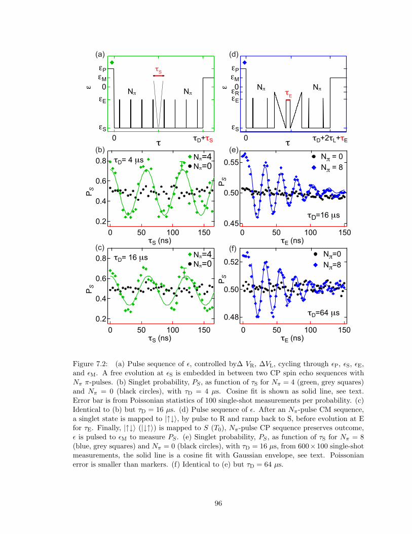
E
Ux ( S)
E
N N
Ux ( S)S
N NE
(a)
(b)
(c)
(d)
(e)
(f)
N =4N =0
N =4N =0
Figure 7.2: (a) Pulse sequence of , controlled by∆ VR, ∆VL, cycling through P, S, E,and M. A free evolution at S is embedded in between two CP spin echo sequences withNπ π-pulses. (b) Singlet probability, PS , as function of τS for Nπ = 4 (green, grey squares)and Nπ = 0 (black circles), with τD = 4 µs. Cosine fit is shown as solid line, see text.Error bar is from Poissonian statistics of 100 single-shot measurements per probability. (c)Identical to (b) but τD = 16 µs. (d) Pulse sequence of . After an Nπ-pulse CM sequence,a singlet state is mapped to |↑↓, by pulse to R and ramp back to S, before evolution at Efor τE. Finally, |↑↓ (|↓↑) is mapped to S (T0), Nπ-pulse CP sequence preserves outcome, is pulsed to M to measure PS . (e) Singlet probability, PS , as function of τS for Nπ = 8(blue, grey squares) and Nπ = 0 (black circles), with τD = 16 µs, from 600×100 single-shotmeasurements, the solid line is a cosine fit with Gaussian envelope, see text. Poissonianerror is smaller than markers. (f) Identical to (e) but τD = 64 µs.
96
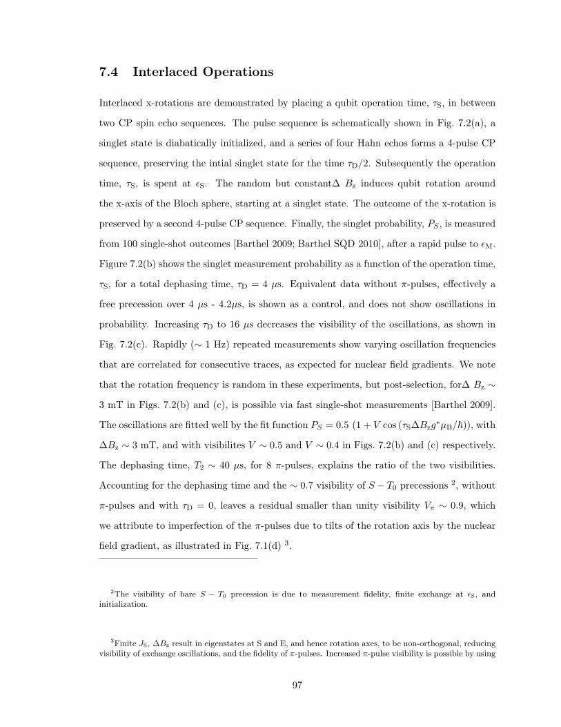
7.4 Interlaced Operations
Interlaced x-rotations are demonstrated by placing a qubit operation time, τS, in between
two CP spin echo sequences. The pulse sequence is schematically shown in Fig. 7.2(a), a
singlet state is diabatically initialized, and a series of four Hahn echos forms a 4-pulse CP
sequence, preserving the intial singlet state for the time τD/2. Subsequently the operation
time, τS, is spent at S. The random but constant∆ Bz induces qubit rotation around
the x-axis of the Bloch sphere, starting at a singlet state. The outcome of the x-rotation is
preserved by a second 4-pulse CP sequence. Finally, the singlet probability, PS , is measured
from 100 single-shot outcomes [Barthel 2009; Barthel SQD 2010], after a rapid pulse to M.
Figure 7.2(b) shows the singlet measurement probability as a function of the operation time,
τS, for a total dephasing time, τD = 4 µs. Equivalent data without π-pulses, effectively a
free precession over 4 µs - 4.2µs, is shown as a control, and does not show oscillations in
probability. Increasing τD to 16 µs decreases the visibility of the oscillations, as shown in
Fig. 7.2(c). Rapidly (∼ 1 Hz) repeated measurements show varying oscillation frequencies
that are correlated for consecutive traces, as expected for nuclear field gradients. We note
that the rotation frequency is random in these experiments, but post-selection, for∆ Bz ∼
3 mT in Figs. 7.2(b) and (c), is possible via fast single-shot measurements [Barthel 2009].
The oscillations are fitted well by the fit function PS = 0.5 (1 + V cos (τS∆Bzg∗µB/)), with
∆Bz ∼ 3 mT, and with visibilites V ∼ 0.5 and V ∼ 0.4 in Figs. 7.2(b) and (c) respectively.
The dephasing time, T2 ∼ 40 µs, for 8 π-pulses, explains the ratio of the two visibilities.
Accounting for the dephasing time and the ∼ 0.7 visibility of S − T0 precessions 2, without
π-pulses and with τD = 0, leaves a residual smaller than unity visibility Vπ ∼ 0.9, which
we attribute to imperfection of the π-pulses due to tilts of the rotation axis by the nuclear
field gradient, as illustrated in Fig. 7.1(d) 3.
2The visibility of bare S − T0 precession is due to measurement fidelity, finite exchange at S, andinitialization.
3Finite JS, ∆Bz result in eigenstates at S and E, and hence rotation axes, to be non-orthogonal, reducingvisibility of exchange oscillations, and the fidelity of π-pulses. Increased π-pulse visibility is possible by using
97
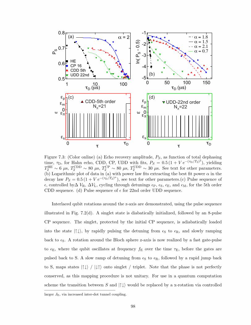
(a)
(b)
(c) (d)CDD-5th order
N =21UDD-22nd order
N =22
Figure 7.3: (Color online) (a) Echo recovery amplitude, PS , as function of total dephasingtime, τD, for Hahn echo, CDD, CP, UDD with fits, PS = 0.5 (1 + V e−(τD/T2)2), yieldingTHE
2 ∼ 6 µs, TCDD2 ∼ 80 µs, TCP
2 ∼ 80 µs, TUDD2 ∼ 30 µs. See text for other parameters.
(b) Logarithmic plot of data in (a) with power law fits extracting the best fit power α in thedecay law PS = 0.5 (1 + V e−(τD/T2)α), see text for other parameters.(c) Pulse sequence of, controlled by∆ VR, ∆VL, cycling through detunings P, S, E, and M, for the 5th orderCDD sequence. (d) Pulse sequence of for 22nd order UDD sequence.
Interlaced qubit rotations around the z-axis are demonstrated, using the pulse sequence
illustrated in Fig. 7.2(d). A singlet state is diabatically initialized, followed by an 8-pulse
CP sequence. The singlet, protected by the initial CP sequence, is adiabatically loaded
into the state |↑↓, by rapidly pulsing the detuning from S to R, and slowly ramping
back to S. A rotation around the Bloch sphere z-axis is now realized by a fast gate-pulse
to E, where the qubit oscillates at frequency fE over the time τE, before the gates are
pulsed back to S. A slow ramp of detuning from S to R, followed by a rapid jump back
to S, maps states |↑↓ / |↓↑ onto singlet / triplet. Note that the phase is not perfectly
conserved, as this mapping procedure is not unitary. For use in a quantum computation
scheme the transition between S and |↑↓ would be replaced by a x-rotation via controlled
larger JE, via increased inter-dot tunnel coupling.
98
∆Bz, as realized in Ref. [Foletti 2009]. The singlet-triplet superposition, with amplitudes
resulting from the z-rotation encoded in its probability amplitudes, is preserved over a
time τD/2 by a second 8-pulse CP sequence. The singlet probability is measured via a
diabatic pulse to M, as discussed above, and subsequently averaged over 600 runs to yield
an electron- and nuclear ensemble. Figure 7.2(e) shows the singlet measurement probability
for a total dephasing time τD = 16 µs, with 8-pulse CP before and after the z-axis rotation,
as function of the rotation time, τE. A control experiment without spin echoes (black
markers) shows no oscillations. Equivalent data for τD = 64 µs is shown in Fig. 7.2(f).
A fit of PS = 0.51 + V cos (JE/τE)e−(τE/T ∗2 )2
agrees well with the data, and yields
JE ∼ 0.2 µeV, and T ∗2 ∼ 100 ns due to gate and charge noise during the exchange operations
and shifts in oscillation frequency and -axis due to the fluctuating∆ Bz, see Fig. 7.1(d). The
visibilities, V ∼ 0.09 for Fig. 7.2(c), and V ∼ 0.06 for Fig. 7.2(c), are rather low 4. The
visibility of bare exchange oscillations is V ∼ 0.3, because of finite∆ Bz during exchange
rotation, and JS at S 5. The remaining loss in visibility is due to T2 ∼ 80µs, the smaller
than one fidelity of the mapping pulse, and of the 16 π-pulses 5. A larger tunnel coupling
between the quantum dots should enable significantly higher visibilities.
7.5 Comparison of different Decoupling Sequences
Performing a CP spin echo sequence strongly improves the coherence time of a separated
singlet, from THE2 ∼ 6 µs for a single Hahn echo to TCP
2 ∼ 80µs for a CP sequence with 16
π-pulses. A singlet is initialized by a diabatic gate-pulse to S, after a Hahn (CP) echo with
total time τD spent at S, the singlet echo recovery amplitude, PS, is measured as the per-
centage of singlet outcomes via a fast gate-pulse to M [Petta 2005; Hahn 1950]. The singlet
echo recovery amplitude, measured from an ensemble of single-shot measurements, is shown
4An offset t0 ∼ 10 ns, due to finite pulse-rise time is taken into account for the fit.
5Finite JS, ∆Bz result in eigenstates at S and E, and hence rotation axes, to be non-orthogonal, reducingvisibility of exchange oscillations, and the fidelity of π-pulses. Increased π-pulse visibility is possible by usinglarger JE, via increased inter-dot tunnel coupling.
99
in Fig. 7.3(a) with an empiric fit of PS = 0.51 + V e−τ2
D/T 22
6. The mechanism of singlet
dephasing determines the functional form of the falloff; PS = 0.51 + V e−(τD/T2)α
is a more
general dephasing time dependence. For a white dephasing spectrum one expects an expo-
nential decay, α = 1 while for coherence solely limited by hyperfine interaction α ∼ 4 is ex-
pected [Witzel 2006; Yao 2006], and has been experimentally observed [Bluhm T2 2010]. We
perform a power law fit to the logarithm of the singlet probability, as shown in Fig. 7.3(b).
For both the HE and CP pulse sequence the best fit is in reasonable agreement with a
Gaussian, with αHE ∼ 1.8 and αCP ∼ 1.5. These powers and comparison of coherence
times to Ref. [Bluhm T2 2010] suggest that the coherence time is limited by inhomogeneous
broadening due to gate voltage drifts and noise shifting the electron wavefunction in the
nuclear field gradient. For a 32-pulse order CP sequence a coherence time of TCP2 ∼ 120 µs
is realized in the device discussed in this paper, while in Ref. [Bluhm T2 2010] a coherence
time T2 ∼ 200 µs has been realized.
In Ref. [Witzel CDD 2007] and Ref. [Uhrig 2007] it has been suggested that more com-
plex pulse sequences outperform a CP pulse sequence for a similar number of π-pulses. The
CDD pulse sequence of nth order is recursively created from two sequences of (n−1)th order
with an additional π-pulse in between them for odd n, the first order is a regular Hahn-echo,
and the 2nd order is identical to a CP sequence with two π-pulses. The pulse cycle with a
5th order CDD sequence, with a total number of 21 π-pulses, is shown in Fig 7.3(c). The nth
order UDD sequence is created, by placing n π-pulses at times δτ = τD sin2 [jπ/(2n + 2)],
where j is the index of the π-pulse. is shown for n = 22 in Fig 7.3(d). Singlet echo recovery
amplitudes for the 5th order CDD and 22nd order UDD sequence are shown in Fig. 7.3(a)
with Gaussian fits, yielding TCDD2 ∼ 80µs for the CDD sequence and TUDD
2 ∼ 30 µs for
the UDD sequence 7. The CDD sequence, with a higher number of π-pulses, does not
6Other parameters in Fig. 7.3(a) are: V HE ∼ 0.6, V CP ∼ 0.6, V CDD ∼ 0.4, V UDD ∼ 0.4. Otherparameters in Fig. 7.3(b) are: V HE ∼ 0.6, THE
2 ∼ 5 µs; V CP ∼ 0.6, TCP2 ∼ 70 µs; V CDD ∼ 0.4, TCDD
2 ∼ 80µs;V UDD ∼ 0.4, TUDD
2 ∼ 17 µs.
7Other parameters in Fig. 7.3(a) are: V HE ∼ 0.6, V CP ∼ 0.6, V CDD ∼ 0.4, V UDD ∼ 0.4. Otherparameters in Fig. 7.3(b) are: V HE ∼ 0.6, THE
2 ∼ 5 µs; V CP ∼ 0.6, TCP2 ∼ 70 µs; V CDD ∼ 0.4, TCDD
2 ∼ 80µs;
100
yield a longer coherence time than the CP sequence, while the coherence time achieved for
the UDD sequence is significantly shorter than for CDD and CP. The discrepancy to the
improvement predicted for UDD in Ref. [Uhrig 2007] may be due to gate voltage drifts8 as
discussed in Ref. [Bluhm T2 2010], or due to the assumption of an ohmic dephasing power
spectrum with a sharp cutoff in Ref. [Uhrig 2007], while the actual power spectrum is of
form ∝ 1/f2 [Reilly 2007]. For a dephasing power spectrum closer to the experiment the
optimal spin echo pulse sequence has been predicted to be very similar to a simple CP
sequence [Pasini 2009], while in Ref. [Lee 2008] it was found that UDD is the optimal se-
quence for nuclear dephasing in GaAs quantum dots.
Acknowledgments
We acknowledge funding from ARO/iARPA, the Department of Defense. This work was
performed in part at the Center for Nanoscale Systems (CNS), a member of the National
Nanotechnology Infrastructure Network (NNIN), which is supported by the National Science
Foundation under NSF award no. ECS-0335765. We thank Hendrik Bluhm, Sandra Foletti,
David Reilly and W. Witzel, for useful discussion.
V UDD ∼ 0.4, TUDD2 ∼ 17 µs.
8Due to the irregular spacings of π-pulses, δτj+1− δτj, the UDD sequence may be more sensitive to driftsand finite rise times of the pulsed gate voltages.
101
Appendix A
Fabrication of Nano-ScaleQuantum Dot Devices
A.1 Overview
In this appendix, I am discussing the fabrication recipe that I used, in its most recent version,
from November 07 2006, given in a step by step guide, that can be easily reproduced.
The devices measured in chapters 3, 4, 5, 6, 7 were all fabricated using the recipe discussed
below.
In one of the two devices in chapter 3 a second metal layer, Permalloy with 84% Nickel
and 16% Iron, was deposited on an insulator layer, to create a micro-magnet on top of
the double dot device. The method used to fabricate the micro-magnet and the difficulties
of the process are discussed in section A.3. For the fabrication back in 2007 the ”Raith”
e-beam writer was used. Also see Jeff Miller’s e-beam guide (available on Marcus group
website 1, under member information).
A.2 Fabrication of Double Quantum Dots
Fabricating quantum dot devices requires patience, discipline and a high tolerance for frus-
tration. The process involves many steps (see section A.4) during any of which the device
can be ruined, due to trivial incidents. I found that it is important not to cut corners
1marcuslab.harvard.edu
102
and to religiously follow the recipe. Small deviations can not only result in failure, but
they will also make the process less comparable to previous and following attempts, making
trouble-shooting impossible.
I fabricated all devices discussed in chapters 3 - 7, using the wafer G050329A, grown
by Micah Hanson in the Gossard group at University of California Santa Barbara. This
wafer showed very good behavior, few switching noise and high reproducibility between
cool-downs.
During Titanium deposition it is important to increase the thermal evaporator power
slowly when heating up boat and material, as the boat may otherwise break. Blow-drying
with nitrogen gas should only be performed with the chip firmly but gently pressed against
a cleanroom wipe. The recipe for metal layer photolithography (see section A.4) has a
comparably low yield (< 80%) which is problematic, because this process needs to be
performed twice. One of these steps has to be performed at the very end of the fabrication
process, which may ruin a week of work. I recommend to replace this process by a different
process of metal deposition that produces an undercut without the need for the photo-resist
LOR3.
A.3 Magnetic Top Layer
The magnetic top layer is the most difficult step in the fabrication of the double dots
with micromagnets (CB3), on which part of the experiments described in chapter 3 were
performed. On top of one of the devices in chapter 3 Permalloy (84% Ni, 16% Fe) was
deposited via thermal evaporation using the CNS evaporator TE4. In the following I list a
few suggestions for future generations of quantum dot devices with micromagnets.
• The Permalloy quite quickly degrades the boats of the evaporator, so it is hard to
deposit more than 100 nm (400 nm are optimal to maximize the magnetic field gradi-
ent [Monzon 1997].). Keeping the deposition rate as low as possible (< 1 A/s) reduced
this problem slightly.
– One solution may be to use electron beam evaporation to deposit the Permalloy.
103

– A better solution may be to switch to Cobalt or a different single-element ferro-
magnet.
– A different boat material or thickness may help too. For the fabrication of CB3
two 0.015” Tungsten boats were used.
• The Permalloy cracks the insulator layer, therefore only a small (micron-size) micro-
magnet was deposited on CB3. The e-beam connector layer is made from Titanium-
Gold. (Separate e-beam exposure and metal deposition are necessary for the ∼ 50 µm
micromagnet and the ∼ 500 µm Ti-Au connector layer.) The photolithography bond
pad layer connecting to the connector layer and used to ground the micromagnet is
also as made from Titanium-Gold.
• The magnetic field gradient was rather small, and potentially absent on some of the
devices.
– One solution may be to use electron beam evaporation to deposit the Permalloy.
– A better solution may be to switch to Cobalt or a different single-element ferro-
magnet.
– A different boat material may help too.
– A thicker anti-oxidation layer of gold on top of the micromagnet may better
prevent surface oxidation.
– I suggest a change to the design in Ref. [Pioro-Ladriere 2008], which creates a
2× larger magnetic field gradient for equal thickness and material.
104

A.4 Fabrication Recipe
Mesa Etch
• prepare 2 chips, real chip and GaAs junk
• 1 a) Photolithography - one layer S1813 - see Photolithography-Mesa-Recipe
• 5 b) Plasma-Clean 5 s, 110 W (directly before etch)
• 1 c) Mesa-Etch - see Mesa-Etch recipe
Ohmic contacts
• 2 a) Photolithography - one layer LOR3, one layer S1818 - see Photolithography-Recipe
• 2 b) Oxygen Plasma-clean 110 W, 5 s
• 2 c) Metal deposition - see Ohmics-Metal-deposition
• 2 c) Liftoff in SVC 175 at 80 degree Celsius until liftoff complete (< 1hour) - seeLiftoff
• 2 d) Clean in IPA for 5 mins, blow-dry with Nitrogen
• 2 e) Thermal Annealing - see Ohmics-Annealing-Instructions
3. and 4. Gates and connector-layer
• If the chip has few devices combine step 3. and 4.
• Do the e-beam step of 3.
• Switch to the 120 micron aperture and do step 4.
• Then deposit both together in one evaporation
• For 22 devices of the double-dot -ESR kind (04/07/06-Chris-ESR) the gates take 55minutes of writing, the connection layer writes in 20 minutes - The device CB4 takes3.1 minutes each at dose 1.48*250 (numbers for Raith)
• Scale and plan accordingly
3. Gates
• 3 a) Do a dose-test on junk-GaAs-material - see E-Beam-Recipe and Dose-Test-Instructions
• 3 b) Do real E-Beam exposure, using the optimum parameters from dose-test - seeE-Beam-Recipe
• 3 c) Develop in 1:3 MIBK:IPA for 60 s, IPA for 30 s, blow-dry
105

• 3 d) UV-ozone clean in prep-room hood 120 s (when using PMMA 950K A4, for C3do 60s)
• 3 e) Metal deposition 50 Angstrom Ti, 150 Angstrom Gold - see gates metal deposition
• 3 f) Liftoff in Acetone > 2 hours (ideally overnight)
NO SONICATION AFTER THIS STEP - only emergencies
4. Connector layer
• 4 a) Expose the connector layer using the 120 micron aperture, either use multiplier1.4 or result from dose-test in step 3 a) (Bigger features tend to need less dose though)
• 4 b) Develop in 1:3 MIBK:IPA for 60 s, IPA for 30 s, blow-dry
• 4 d) UV-ozone clean in prep-room hood 120 s
• 4 e) Metal deposition 50 Angstrom Ti, 150 Angstrom Gold
• 4 f) Liftoff in Acetone > 2 hours (possibly overnight)
5. Photolithography layer
• 5 a) Photolithography - one layer LOR3, one layer S1818 - see Photolithography-Recipe
• 5 b) Plasma-Clean 5 s, 110 W (directly before Metal deposition)
• 5 c) Metal deposition - see Photolithography-Metal-Deposition-Insctructions
• 5 d) Liftoff in SCV 175 at 80 degree Celsius < 1 hr - see Liftoff
• 5 d) Clean in IPA for 5 minutes, blow-dry
Below here only for 2 - layer chips
6. Insulator-Layer (if a second metal layer is needed)
• 6 a) 3 -solvent clean, no sonication
• 6 b) Test deposition of 35 nm (ESR) on junk GaAs and Silicon - see ALD-Instructions
• 6 c) Observe GaAs layer under microscope, check homogeneity
• 6 d) Measure thickness of layer on Silicon chip with ellipsometer
• 6 e) Scale number of cycles according to height deviations
• 6 f) Deposit on real chip - see ALD-instructions
106

7. Top-gates
• 7 a) Perfor dose-test on previously insulator-deposited junk GaAs - 10 micron aperture- see E-Beam-Recipe
• 7 b) Do real E-Beam exposure, using the optimum parameters from dose-test - seeE-Beam-Recipe at 10 micron - Magnetic-Ebeam-Recipe
• 7 d) Develop in 1:3 MIBK:IPA for 120 s, IPA for 10 s, blow-dry
• 7 e) UV-ozone clean in prep-room hood 120 s (for PMMA 950 K A4)
• 7 f) Metal deposition of 5 nm of Titanium, 250 nm Permalloy at < 0.1 nm/s and a15 nm of Gold as a anti-oxidation cap, see Magnet-Layer-Metal-Deposition-Recipe
• 7 g) Liftoff in Acetone > 12 hours
8. Connector layer
• 8 a) Expose the connector layer using the 10 micron aperture, either use multiplier1.4 or result from dose-test in 7 a) (Bigger features tend to need less dose though) seeE-Beam-Recipe
• 7 d) Develop in 1:3 MIBK:IPA for 120 s, IPA for 10 s, blow-dry
• 7 e) UV-ozone clean in prep-room hood 120 s (for PMMA 950 K A4)
• 7 f) Metal deposition of 5 nm of Titanium, 250 nm Gold at < 0.1 nm/s , see Magnet-Layer- Metal-Deposition-Recipe
• 7 g) Liftoff in Acetone > 12 hrs
9. Magnetic photolithography layer
• 9 a) Photolithography - 1 layer LOR3, one layer S1818 - see Photolithography-Recipe
• 9 b) Plasma-Clean 5 s, 110 W(directly before Metal deposition)
• 9 c) Metal deposition - see Photolithography-Metal-Deposition-Instructions
• 9 d) Liftoff in SCV 175 at 80 degree Celsius < 1 hr - see Liftoff
• 9 d) Clean in IPA for 5 minutes, blow-dry
107

A.5 Detailed Fabrication Steps
1. Device photolithography for mesas
1.1 Switch on mask aligner
• Let Lamp warm up for > 30 minutes.
1.2. Three solvent clean
Sonicate during all three solvent cleans.
1. TCE 5 mins
2. Acectone 5 mins
3. IPA 5 mins
4. Blow-dry with compressed Nitrogen gas, careful not to blow away chip - press chipdown on paper
1.2. Singe on center of a hotplate at 200 degree Celsius for 5 mins
1.3. Spin resists
• Spin junk chip first.
• Cover drain of spinner!
1. Spin 1813
• 500 RPM for 5 s (1 s spin-up)
• 4000 RPM for 60 s (1 s spin-up)
2. Bake @ 115 degree Celsius for 2 mins
1.4. Develop
1. Use mask aligner to perform photolithography with appropirate mask, expose for 4seconds
2. Rinse in CD 26 for 60 seconds
3. Rinse in DI water for 20 secs
4. Blow dry with compressed Nitrogen gas
1.5. Finish and prepare for etch
1. Observe under RED FILTER optical microscope or under alignment microscope
2. Plasma-Clean @ 110 W for 5 secs (at about 0.9 Torr before discharge starts)
108

Starting over, in case of accident
Just do a 3-solvent clean with sonication → chip will be clean.
2. Mesa-etch-recipe
2.1. Mixing
• Get H2O2 bottle from refrigerator, and Marcus-glass-ware box
• mix 1:8:240 H2SO4:H2O2:H2O, stir
• prepare one to two beakers of DI water
2.2. If you do not know the approximate etch-rate
(e.g. if you have not used the chemicals recently)
• Do etching procedure (2.3.) on a GaAs junk chip first
• Determining etch-rate by measuring time, and the etched depth (via profilometer)
• If you know the material well, skip and directly proceed with real chip
2.3. Etch
1. Measure and write down the height of 4 mesa-resist piles at opposite edges of chip
2. Dunk chip into solution for time t, where t = h/(3 a)
• h is the desired height (for 110 nm 2DEG depth ∼ 140 nm)
• a is the known (or measured on junk chip) etch rate
• My last etch: a = 128nm/43 s
3. use profilometer to measure the four mesas measured before etch
4. recalculate a and proceed with second etching step, for t = h/(2 a), where h is thedistance still missing
5. When desired height is reached, liftoff resist in acetone for 5 mins in sonication, cleanin IPA, blow-dry
6. Measure height of mesas, calculate average a
2.4. Clean up and bring H2O2 back to fridge
3. Photolithography for metal liftoff
(for Ohmic contacts or top gate contact layer)
3.1 Switch on Mask aligner
• Let Lamp warm up for > 30 minutes.
109
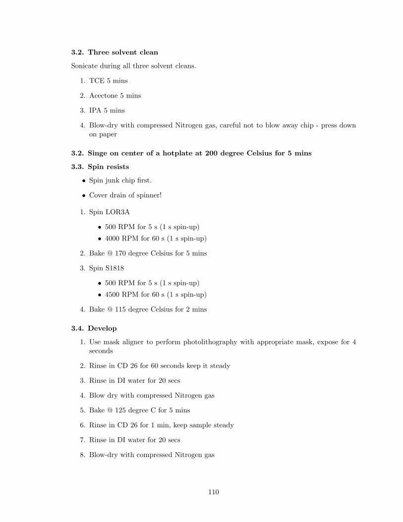
3.2. Three solvent clean
Sonicate during all three solvent cleans.
1. TCE 5 mins
2. Acectone 5 mins
3. IPA 5 mins
4. Blow-dry with compressed Nitrogen gas, careful not to blow away chip - press downon paper
3.2. Singe on center of a hotplate at 200 degree Celsius for 5 mins
3.3. Spin resists
• Spin junk chip first.
• Cover drain of spinner!
1. Spin LOR3A
• 500 RPM for 5 s (1 s spin-up)
• 4000 RPM for 60 s (1 s spin-up)
2. Bake @ 170 degree Celsius for 5 mins
3. Spin S1818
• 500 RPM for 5 s (1 s spin-up)
• 4500 RPM for 60 s (1 s spin-up)
4. Bake @ 115 degree Celsius for 2 mins
3.4. Develop
1. Use mask aligner to perform photolithography with appropriate mask, expose for 4seconds
2. Rinse in CD 26 for 60 seconds keep it steady
3. Rinse in DI water for 20 secs
4. Blow dry with compressed Nitrogen gas
5. Bake @ 125 degree C for 5 mins
6. Rinse in CD 26 for 1 min, keep sample steady
7. Rinse in DI water for 20 secs
8. Blow-dry with compressed Nitrogen gas
110

3.5. Finish and prepare for metal deposition
1. Observe under RED FILTER optical microscope
2. Plasma-Clean at 110 W power, for 5 secs (at about 0.9 Torr, before discharge starts)
4. Metal-deposition for ohmic contacts
• DO A JUNK CHIP FIRST
4.1 Electron-beam plasma clean
• 5s at 110 W
• Do NOT do UV-clean instead!
Minimize time between 4.2. and 4.3.!
• Perform 4.2 and 4.3 for junk-chip first, then for the real chip
• Prepare Metal deposition before etching in step 2. (vent and open evaporator EE3)
4.2. Ammonium-Hydroxide-etch
1. Fill glass beaker with Ammonium-Hydroxide from 30% bottle (29 % works too)
2. Dip chip into glass beaker with base for 2 seconds - use timer!
3. Clean in DI water and blow-dry thoroughly
4.3. Prepare metal deposition
1. Attach chip to holder with double sided tape, make the tape dirty (otherwise chipdoes not come off)
2. Open evaporator and confirm metal positions / place Marcus sources into evaporator
3. Load sample into evaporator, pump down below 10−5 mbar
4.4. Metal gas-out
• When pressure reached low 10−6 mbar, switch on power supply
• Gas out all sources by evaporating a few nanometers each (with shutter closed!)
4.5. Evaporate metal
• Wait for pressure to go down again, then deposit:
1. 5 nm of Pt at 0.1 nm/s
2. 160 nm of Au at 0.3 nm/s
3. 80 nm of Ge at 0.25 nm/s
111

4. 53 nm of Pt at 0.15 nm/s
5. 51 nm of Au at 0.3 nm/s
4.6. Unload sample after switching off power, and venting
5. Metal liftoff for photo-lithography layers
1. Prepare SVC 175
• let sit on hotplate at 80 deg Celsius for > 5 minutes
2. Liftoff - CHIP MUST NOT GET DRY!
(a) Lower chip in SVC
(b) Check after 20 mins, squirt IPA onto submerged chip (Do not let it dry!)
(c) Park chip in IPA, replace SVC
(d) Observe chip (still in IPA) under microscope
(e) Go on in steps of 10 mins / 20 mins, repeating the IPA / replacement step untilliftoff complete
(f) Observe in IPA to check whether the metal has indeed been completely lifted offand that there are no LOR stains
(g) Throw in fresh SVC for 5 mins, if there is metal or resist left
3. Leave in IPA for 5 mins
4. Blow-dry
6. Annealing of ohmic contacts
1. Switch On Annealer
2. Put in junk material with metal film on top
• choose recipe CB1, which is just Jason’s JRP1 copied over in early June 06
• check recipe - should go up to 525 deg Celsius
• pay attention that the actual temperature reaches the set temperature duringtest-run
• take out chip after cooldown is finished
3. Observe under microscope - should look like the chip in the notebook (not cleanroom)from 04/11/06 ”bubbly”
4. repeat 2. with real chip
5. Switch off Annealer
• Test Ohmic contacts in 4 K dunker
112

7. Electron beam recipe
7.1. Three solvent clean, if this is the first e-beam layer
Sonicate during all three solvent cleans.
1. TCE 5 mins
2. Acectone 5 mins
3. IPA 5 mins
4. Blow-dry with compressed Nitrogen gas, careful not to blow away chip - press downon paper
7.2. Prebake at 170 degree C for 2 minutes
7.3. Spin 950k PMMA A4
• Spin 500 R.P.M. for 5 seconds, 1 second spin-up - Put on resist in this step
• Spin 4000 RPM for 60 seconds with a 1k/second acceleration.
7.4. Bake for 15 minutes at 170 degree C
7.5. Load sample into the Raith.
Put a small amount of silver paint on the corners of the chip for coarse focusing, do not useAcetone to solve paint. Let dry for 5-10 minutes.
7.6. Tune up the Raith
Follow Jeff Miller’s e-beam guide. See Marcus lab member information page.
7.7. Expose pattern
• Use Voltage 30 kV, Area dose = 250, line dose = 1500, step size of 6 nm.
• For gates use 10 micron aperture and do focusing on burnt spots (see Jeff’s e-beamguide)
• For connector layer use 120 micron aperture and 20 nm step size
• Focus roughly at 10 micron and save the positions. (With the 120 aperture the beamexposes too fast, rough focusing on alignment marks is sufficient.)
Remark on dose tests
Expose a dose matrix with a dose factor ranging from 1 to 2 (or 2.2) in steps of 0.04.Expose the first dose-test over a 50x50 microns. For the remainder of the dose test restrictthe pattern to 10 x 10 microns around the center. This way, the dose test runs faster. (seedose test instructions)
113
7.8. Expose features
• Create position-list according to translations between mesas on chip.
• Use one of the alignment marks as zero-point of your coordinate system.
7.9. Develop for 60 seconds in 1:3 MIBK:IPA
7.10. Rinse in IPA for 30 seconds and blow dry.
7.11. UV ozone clean
Using the cleaner in Marcus lab sample prep-room hood for 120 seconds.
7.12. E-Beam evaporation, immediately after previous step.
Using TE-3 or TE-5 in CNS cleanroom.
• 50 angstroms of Ti at 0.5 Angstrom per second.
• 150 angstroms of Au at 0.5 Angstroms per second.
7.13. Liftoff in acetone for > 2 hours.
Spray with isopropanol and blow dry. Do not let acetone dry on the chip or it will beruined.
8. Metal-deposition for e-beam gates
Using TE-3 or TE-5 in CNS cleanroom.
8.1. Load sample into thermal evaporator
1. Open evaporator, close all pumps, then vent
2. Load Ti into crucible holder 2, Gold into crucible holder 3
3. Add backup of Ti into crucible 1
4. Attach chip to holder with double sided tape, make the tape dirty
5. Pre-pump using roughing pump, down to 2E-1Torr
6. Close roughing valve, open high vacuum valve
8.2. Metal gas-out
after about 30 mins to 1 hr
1. Degas Ion-gauge
2. when reached the low 10E-6 or ideally high 10E-7 pressures (≤ 2× 10⁻⁶ Torr) switchON Power supply
3. turn up current slowly, wait until current equilibrates (approx 10 A / 10 secs )
114
4. Ti: careful - will not melt until really high current and then practically explode andjump to 3 nm/s, observe boat with sun glasses TUNE down current immediately Timelts anywhere btw. 150 and 190 Amp with 0.15” Tungsten boats
5. gas out all sources (shutter closed)
6. possibly evaporate 10 nm of Titanium again which lowers the pressure strongly
8.3 Evaporate metal
• Wait for pressure to go down again, for about 1 hour.
Deposit:
• 5 nm of Ti at 0.05 nm/s
• 15 nm of Au at 0.05 nm/s
8.4 Unload sample
• Switch off power
• CLOSE ”HIGH VAC”, cryopump valve
• Vent evaporator
• Take sample off carefully, use razor-blade, don’t lever it up but circle around it pro-truding deeper underneath each time
9. Insulator-layer, via Atomic Layer Deposition (ALD)
1. Load sample into ALD in sample preparation room
(a) close stop-valve, set flow to 100(b) open after at room pressure(c) put sample in the center(d) close lid, open stop valve(e) OPEN precursor valve
2. Set cycles
(a) Set flow to 20(b) Set delay to 5 mins(c) Set valve 0 open time to 0.1 s(d) Set valve 1 open time to 0.1 s(e) Set pump time to 5 seconds each(f) Set Expose time to 0 seconds(g) Set number of cycles
• Assume 0.9 nm / cycle but compare to values in logbook, do a test-run if indoubt or if thickness is critical.
115

Date Substrate Cycles Thickness Deposition rate Comments04/24/06 Si-wafer 31 ± 1 nm 342 0.091 nm / cycle -04/25/06 Si-testchip 39.5 nm 427 0.093 nm/cycle -04/29/06 Si-testchip 33.8 nm 390 0.087 nm/cycle -
Table A.1: ALD deposition rate from past depositions.
3. Press Start
4. Wait
5. Close Stop Valve when done - set flow to 100
6. Take out sample, Close lid and set flow to 20
7. Close precursor
10. Metal-deposition for magnetic top layer
10.1. Load sample into TE 4
1. Open evaporator, close all pumps, then vent the system.
2. Load Permalloy, 84% Ni, 16% Fe into crucible holders 1 and 2 (backup boat)
3. Load gold into crucible holders 3 and 4 (backup boat)
4. Attach chip to holder with double sided tape, make the tape dirty to avoid breakingof chip during removal.
5. Prepump roughing pump until 2E-1Torr
6. Close roughing valve, open high vacuum valve
10.2. Metal gas-out
After pumping for about 0.5− 1hours, after reaching the low 10−6 Torr pressures
1. Switch ON Power supply
2. Turn up current slowly, wait until current equilibrates (approx 1 A / s )
3. Out-gas all sources (shutter closed!)
10.5. Evaporate Metal
Wait for pressure to go down again for about 1 hour.
• Deposit:
– 5 nm of Titanium
• Shutter closed:
– 10 nm of Permalloy
116
• Open shutter
– 100 nm of Permalloy at < 0.1 nm/s
– 15 nm of Gold at 0.1 nm/s as a cap against oxidation
10.6. Take out after switching off power and venting CLOSE HIGH VACFIRST!
10.7. Take sample off carefully (use razor-blade)
11. Metal deposition on photolithography layers (non-ohmic)
(for top gate contact layer)
11.1. Load sample into TE 3
1. Open evaporator, close all pumps, then vent
2. Load Ti into crucible holder 2, Gold into crucible holder 3
3. Attach chip to holder with double sided tape, make the tape dirty
4. Prepump roughing pump until 2× 10⁻¹Torr
5. Close roughing valve, open high vacuum valve
11.2. Metal gas-out
After about 30 mins, when low 10−6 Torr pressures are reached (around 2 × 10⁻⁶ Torr)switch on power supply.
• Turn up current slowly, wait until current equilibrates (∼ 0.1 nm/s)
• Out-gas all sources (shutter closed)
• Evaporate 10 nm of Titanium again which lowers the pressure strongly
11.3. Evaporate metal
Wait for pressure to go down again, for about 1 hour. Deposit:
• 5 nm of Ti at 0.05 nm/s
• 200 nm of Au at 0.3 nm/s
(The height of the Gold-layer should be 10 nm higher than the highest mesa.)
11.4. Take out after switching off power, CLOSING HIGH VAC valve, andventing
11.5. Take sample off carefully (use razor-blade)
117
Appendix B
Reflectometry for fast QuantumDot Charge-Sensing andSingle-Shot Measurements
B.1 Introduction
B.1.1 Motivation
For charge measurements in quantum dots, in particular for applications in spin measure-
ments for quantum information processing, it is desirable to detect the conductance of a
charge sensor at high bandwidth and with low noise [Schoelkopf 1998]. The charge sensor
in question can be a quantum point contact (QPC) [Reilly APL 2007], a single electron
transistor (SET) [Schoelkopf 1998], or a sensor quantum dot (SQD) [Barthel SQD 2010],
conceptually similar to a SET. Aside from high bandwidth it is also desirable to work at
high frequencies because of 1/f noise from the electronics and from the sample itself, e.g.
charge noise in a GaAs two dimensional electron gas.
The high resistance of the charge sensors, which are typically operated at conductances,
g < 0.5 e2/h, where they are most sensitive to their local electric potential [Field 1993;
Barthel SQD 2010], poses a fundamental challenge obtaining high bandwidth and opera-
tion frequencies in charge detection setups. At the typical conductances, g ∼ 0.25e2/h, the
resistance is, R ∼ 100 kΩ, which together with the typical capacitances, C > 100pF, of
dilution refrigerator dc wiring, sets an upper limit for the applied frequencies for sensing
currents and for the bandwidths that can be obtained. The bandwidth fRC for a QPC
118

measured at g ∼ 0.25 e2/h with fridge wiring capacitance C ∼ 500pF is
fRC =1
2π R C=
12 π 100 kΩ 500 pF
∼ 3 kHz. (B.1)
B.1.2 Reflectometry
Reflectometry is one of the key constituents that enabled the fast and sensitive measure-
ments in chapters 4 - 7. As discussed in section B.1.1 it is desirable to measure electronic
systems at higher frequencies to avoid 1/f noise, a goal that is complicated by the low
RC bandwidth of high impedance devices [Eq. B.1]. The reflectometry setup used in the
experiments of this thesis was only slightly modified after being implemented by David
Reilly as described in Ref. [Reilly APL 2007]. RF-reflectrometry was originally developed,
implemented and described in Ref. [Schoelkopf 1998].
In reflectometry the resistance of the device of interest, like a charge sensor, is measured
indirectly via the damping of a resonant rf-circuit. The so called tank circuit, schematically
shown in Fig. B.1(b), is an LCR circuit, and behaves as a resistance matching network when
used in reflectometry measurements.
In rf- or microwave circuits electromagnetic waves are reflected at interfaces between
elements that have different impedance Z. If the impedances of the source circuit, e.g.
rf-generator and coaxial connections, are equal to the coupled element, the power emitted
from the sources is completely absorbed by the coupled element. This is the case for a
standard rf-terminator which, at 50 Ω, absorbs the power emitted from a 50 Ω transmission
line, e.g. a standard coaxial cable, completely. Otherwise, part of or all of the power is
reflected back into the source. The reflection coefficient, for the voltage amplitude, at an
interface between a source with impedance Z0 and a circuit element with impedance Z is
Γ =Z − Z0
Z + Z0, (B.2)
as derived in great detail in Ref. [Pozar 1988].
The key of using a tank circuit in the measurement of high electronic devices is to
match a certain set-resistance of the measured device to the source, such that Z = Z0.
119
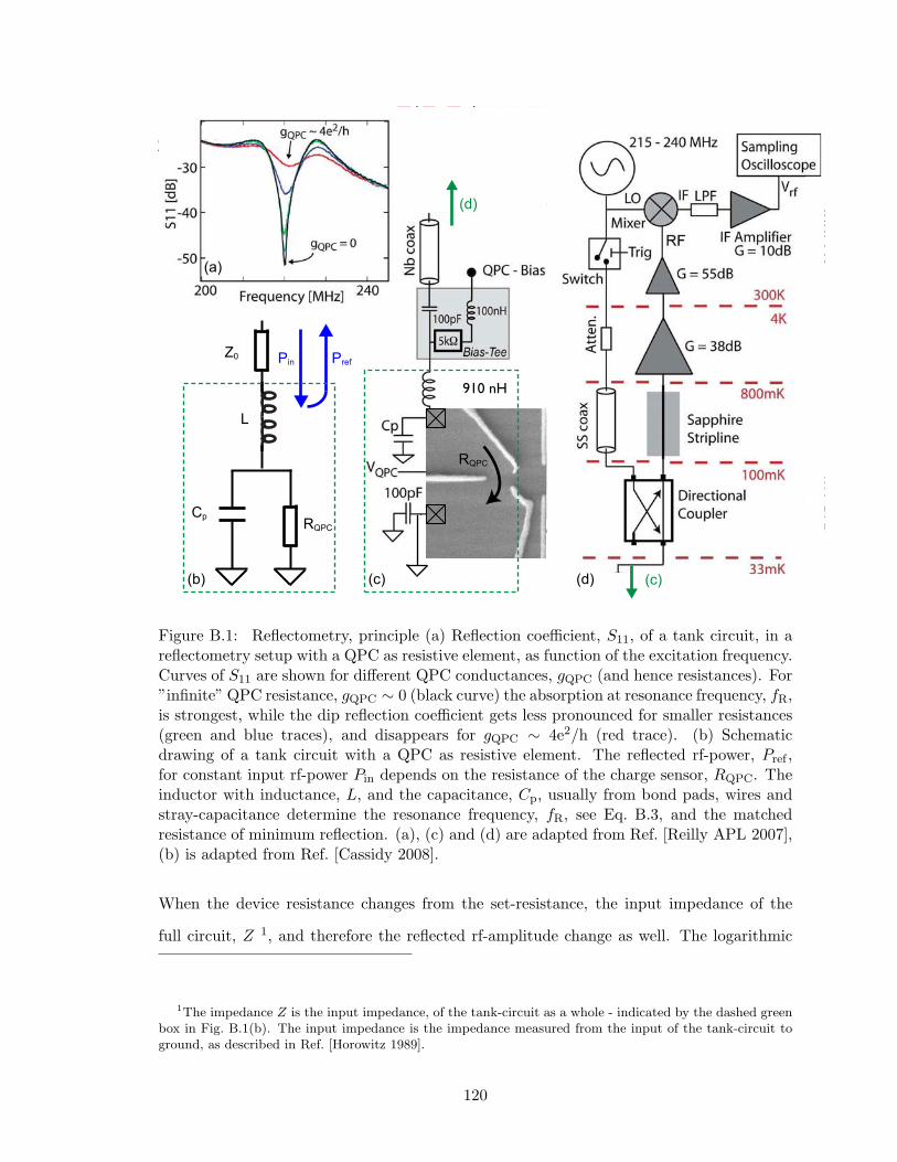
910 nH910 nH
RQPC
C P
LZ 0
R QPC
P in
P ref
Cp RQPC
Z0 Pin Pref
2
FIG. 1: (Color online) (a) Schematic of measurement setupincluding false-color SEM image of a representative device.Gates shaded green are held at ∼ 1V throughout. Niobiumcoax and ∼ 50 Ω ohmic contacts minimize losses betweensample and cryogenic amplifier. A stripline fabricated on asapphire substrate is used to thermalize the inner conductorof the Nb coax. Demodulation is performed by mixing theRF signal with a local oscillator (LO) to yield an interme-diate frequency (IF) that is low-pass filtered (LPF) beforefurther amplification and digitization. (b) Photograph of rfcircuit board showing sample, matching circuit and compo-nents used to make a bias-Tee. (c) Reflection coefficient S11of impedance transformer with changing gQPC (resonance at220.2 MHz). (d) Demodulated response (Vrf) measured si-multaneously with dc conductance as the QPC gate (shadedblue in SEM image) bias is varied (VL = -700mV). Dashed lineindicates bias point for charge sensing. Inset shows transferfunction of Vrf verses conductance. (e) Demodulated time-domain response to 50 MHz gate signal with QPC biased to∼ e2/h and matching inductance reduced to 560 nH (differentdevice to all other measurements presented).
FIG. 2: (Color online) (a) AM response of rf-QPC to 1 MHzgate modulation, VR = 0.7 mV (rms). SNR of sidebandsyields a sensitivity Sg = 5 × 10⁻⁶e2/h Hz−1/2. (b) SNR ofupper sideband as a function of modulation frequency. Redcurve is a guide to the eye. (c) SNR of upper sideband as afunction of carrier power. (d) SNR of upper sideband as afunction of carrier frequency, consistent with Fig. 1(c). AllSNR measurements made in a resolution bandwidth of ∆f =10 kHz.
FIG. 3: (Color online) (a) Derivative of Vrf (in arbitary units)as a function of VL and VR, magnetic field B = 100 mT. VL
is rastered at ∼ 1 mV/150 µs (∼ 106 data points acquired in∼ 180 s). Labels indicate number of electrons in the left andright dots.
width ∆f . This SNR gives a conductance sensitivitySg = (1/2)dgQPC(∆f)−1/210−SNR/20, where the factor1/2 accounts for power collected from both sidebands, of5×10−6e2/h Hz−1/2. This sensitivity allows, for instance,a dgQPC = 0.01 e2/h conductance change to be measuredwith unity SNR in τint = 500 ns. Above ∼ 8 MHz, theQ-factor (∼ 15) of the impedance matching circuit limitsthe sensitivity as shown in Fig. 2(b). The SNR increaseswith applied carrier power [Fig. 2(c)] up to the energy
(a)
(b) (c) (d)
(d)
(c)
L
Figure B.1: Reflectometry, principle (a) Reflection coefficient, S11, of a tank circuit, in areflectometry setup with a QPC as resistive element, as function of the excitation frequency.Curves of S11 are shown for different QPC conductances, gQPC (and hence resistances). For”infinite” QPC resistance, gQPC ∼ 0 (black curve) the absorption at resonance frequency, fR,is strongest, while the dip reflection coefficient gets less pronounced for smaller resistances(green and blue traces), and disappears for gQPC ∼ 4e2/h (red trace). (b) Schematicdrawing of a tank circuit with a QPC as resistive element. The reflected rf-power, Pref ,for constant input rf-power Pin depends on the resistance of the charge sensor, RQPC. Theinductor with inductance, L, and the capacitance, Cp, usually from bond pads, wires andstray-capacitance determine the resonance frequency, fR, see Eq. B.3, and the matchedresistance of minimum reflection. (a), (c) and (d) are adapted from Ref. [Reilly APL 2007],(b) is adapted from Ref. [Cassidy 2008].
When the device resistance changes from the set-resistance, the input impedance of the
full circuit, Z 1, and therefore the reflected rf-amplitude change as well. The logarithmic
1The impedance Z is the input impedance, of the tank-circuit as a whole - indicated by the dashed greenbox in Fig. B.1(b). The input impedance is the impedance measured from the input of the tank-circuit toground, as described in Ref. [Horowitz 1989].
120
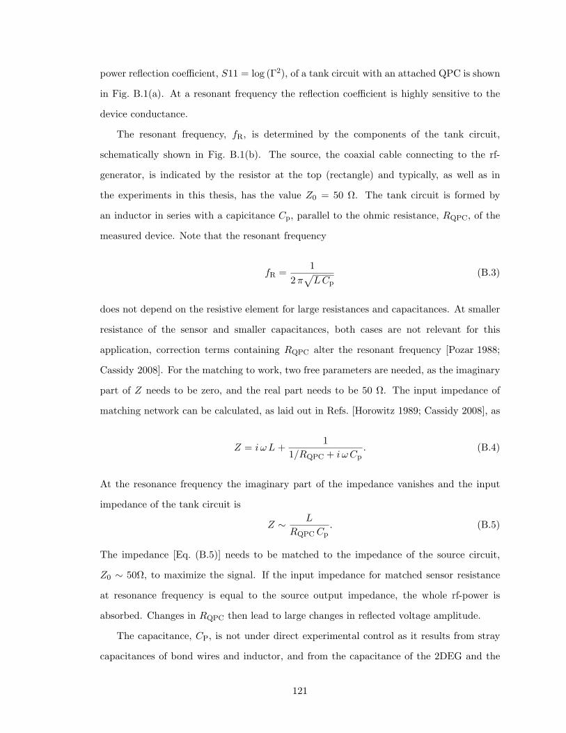
power reflection coefficient, S11 = log (Γ2), of a tank circuit with an attached QPC is shown
in Fig. B.1(a). At a resonant frequency the reflection coefficient is highly sensitive to the
device conductance.
The resonant frequency, fR, is determined by the components of the tank circuit,
schematically shown in Fig. B.1(b). The source, the coaxial cable connecting to the rf-
generator, is indicated by the resistor at the top (rectangle) and typically, as well as in
the experiments in this thesis, has the value Z0 = 50 Ω. The tank circuit is formed by
an inductor in series with a capicitance Cp, parallel to the ohmic resistance, RQPC, of the
measured device. Note that the resonant frequency
fR =1
2 π
L Cp(B.3)
does not depend on the resistive element for large resistances and capacitances. At smaller
resistance of the sensor and smaller capacitances, both cases are not relevant for this
application, correction terms containing RQPC alter the resonant frequency [Pozar 1988;
Cassidy 2008]. For the matching to work, two free parameters are needed, as the imaginary
part of Z needs to be zero, and the real part needs to be 50 Ω. The input impedance of
matching network can be calculated, as laid out in Refs. [Horowitz 1989; Cassidy 2008], as
Z = iωL +1
1/RQPC + iωCp. (B.4)
At the resonance frequency the imaginary part of the impedance vanishes and the input
impedance of the tank circuit is
Z ∼ L
RQPC Cp. (B.5)
The impedance [Eq. (B.5)] needs to be matched to the impedance of the source circuit,
Z0 ∼ 50Ω, to maximize the signal. If the input impedance for matched sensor resistance
at resonance frequency is equal to the source output impedance, the whole rf-power is
absorbed. Changes in RQPC then lead to large changes in reflected voltage amplitude.
The capacitance, CP, is not under direct experimental control as it results from stray
capacitances of bond wires and inductor, and from the capacitance of the 2DEG and the
121
Ohmic contacts. Therefore, CP will vary between nominally identical devices, and to some
extent even between different cool-downs of the same device (but only by few percent). The
typical value of the tank circuit capacitance for the devices in this thesis is CP ∼ 0.5 pF,
see Appendix C.
The matching resistance is therefore controlled via the rf-frequency and the inductance,
L. The cold amplifier, see section B.2, has a finite gain bandwidth of typically ∼ 40 MHz
around a center frequency which was ∼ 230 MHz for the amplifier used in the experiments
in chapters 4-7. In general one frequency, fR, that is suitable for the application 2 is chosen
when designing or ordering the customized rf-amplifier.
With the frequency constrained to the amplifier gain window after design, the induc-
tance, L, is the only parameter that can be changed for fine-tuning during device cool-down.
However, most coils develop a self-capacitance at high inductances, usually quoted as self-
resonant frequency. This limits the freedom in the choice of matched resistance RQPC, and
it is not always possible to achieve RQPC ∼ 100 kΩ, as desirable for charge sensors. It
is advisable to reduce the capacitance Cp by keeping bondwires of the sensors short and
avoiding cross coupling to wires of other connections. For the experiments in chapters 4 -
7, the inductance was L = 910 nH. Matching was achieved for g ∼ 0.4e2/h, ideal for charge
sensing.
The inductors were obtained from coilcraft 3. Free test-kits of inductors with a wide
range of inductances can be ordered from them by email.
B.2 Reflectometry Measurement Setup
The reflectometry setup used in the experiments in chapter 4 and 5 is shown in Figs. B.1(c)
and B.2. Figure B.2 shows the room temperature components in more detail. The rf-
2For GaAs QPCs and SQDs a center frequency, fR ∼ 230 MHz, of the amplifier gain window is a goodchoice.
3www.coilcraft.com
122
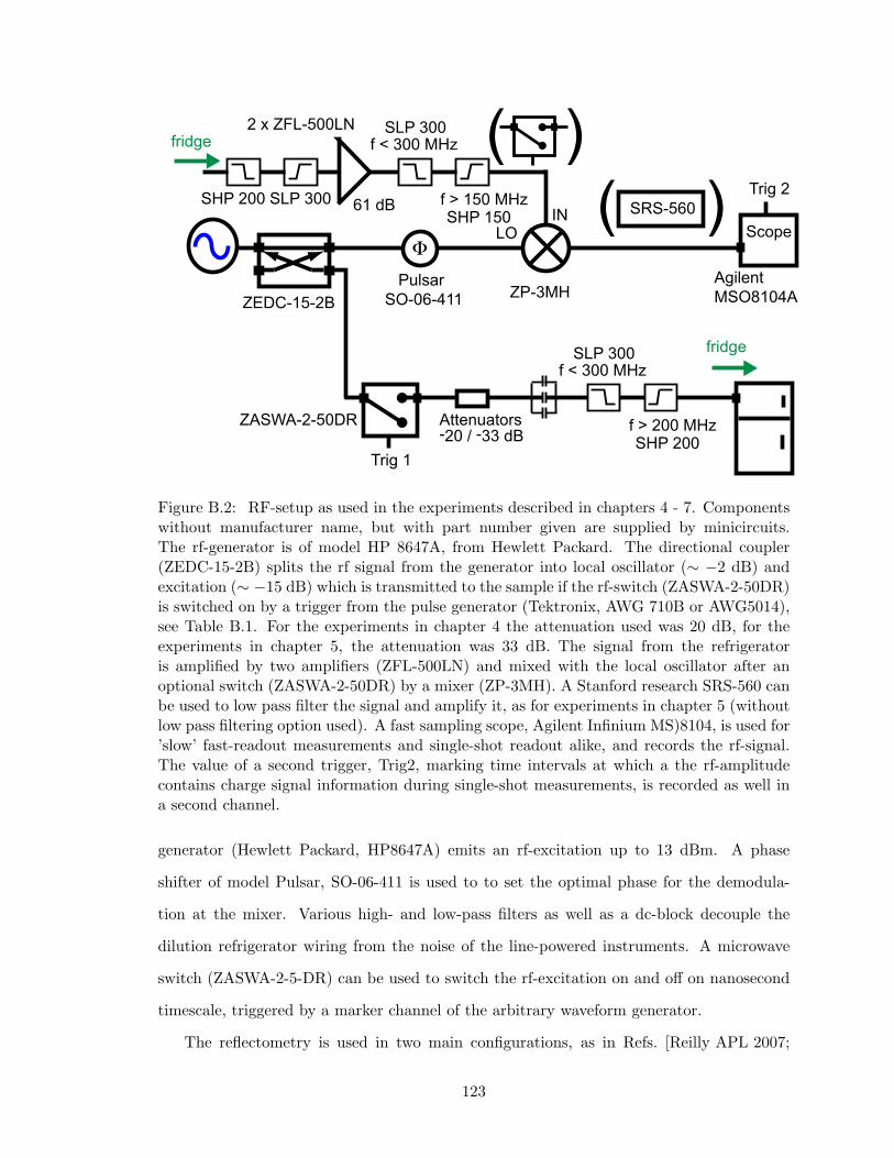
fridge
LO
Trig 1
ZEDC-15-2B
ZASWA-2-50DR Attenuators-20 / -33 dB f > 200 MHz
f < 300 MHzSLP 300
SHP 200
ZP-3MH
fridge
f > 150 MHz
f < 300 MHzSLP 300
SHP 150 IN61 dBSLP 300SHP 200
2 x ZFL-500LN
SRS-560( )Scope
AgilentMSO8104A
( )
PulsarSO-06-411
Trig 2
Figure B.2: RF-setup as used in the experiments described in chapters 4 - 7. Componentswithout manufacturer name, but with part number given are supplied by minicircuits.The rf-generator is of model HP 8647A, from Hewlett Packard. The directional coupler(ZEDC-15-2B) splits the rf signal from the generator into local oscillator (∼ −2 dB) andexcitation (∼ −15 dB) which is transmitted to the sample if the rf-switch (ZASWA-2-50DR)is switched on by a trigger from the pulse generator (Tektronix, AWG 710B or AWG5014),see Table B.1. For the experiments in chapter 4 the attenuation used was 20 dB, for theexperiments in chapter 5, the attenuation was 33 dB. The signal from the refrigeratoris amplified by two amplifiers (ZFL-500LN) and mixed with the local oscillator after anoptional switch (ZASWA-2-50DR) by a mixer (ZP-3MH). A Stanford research SRS-560 canbe used to low pass filter the signal and amplify it, as for experiments in chapter 5 (withoutlow pass filtering option used). A fast sampling scope, Agilent Infinium MS)8104, is used for’slow’ fast-readout measurements and single-shot readout alike, and records the rf-signal.The value of a second trigger, Trig2, marking time intervals at which a the rf-amplitudecontains charge signal information during single-shot measurements, is recorded as well ina second channel.
generator (Hewlett Packard, HP8647A) emits an rf-excitation up to 13 dBm. A phase
shifter of model Pulsar, SO-06-411 is used to to set the optimal phase for the demodula-
tion at the mixer. Various high- and low-pass filters as well as a dc-block decouple the
dilution refrigerator wiring from the noise of the line-powered instruments. A microwave
switch (ZASWA-2-5-DR) can be used to switch the rf-excitation on and off on nanosecond
timescale, triggered by a marker channel of the arbitrary waveform generator.
The reflectometry is used in two main configurations, as in Refs. [Reilly APL 2007;
123
Reilly 2007] - in fast readout, or for single-shot measurements as in Ref. [Barthel 2009;
Barthel SQD 2010].
B.2.1 Fast Readout
Due to the high bandwidth and signal-to-noise ratio of the reflectometry setup the measure-
ment integration is no longer the bottleneck of the measurement (dc-QPC measurements
typically average 100 ms per datapoint). The limitation now lies in the changing of gate
voltages. For the measurement of charge stability diagrams or in order to measure ensemble
averages of pulsed experiments as in Refs. [Reilly 2007; Reilly Diff. 2008; Reilly 2008], one
of the double dot plunger gate voltages VL or VR (see chapter 2, Fig. 2.5(a)) is rapidly
ramped with a sawtooth waveform at ∼ 40 Hz. The ramping is achieved by simply adding
the output of a Hewlett Packard HP 30250A function generator to one of the digital to
analog converter (DAC) channels that provide the voltages, VL and VR. Triggering the os-
cilloscope on the marker from the function generator encodes the gate-voltage information
in the time axis of the scope [Reilly APL 2007].
The gate voltage opposite of the charge sensor is ramped, in order to minimize parasitic
gating of the sensor. This allows to measure a whole column in a charge stability diagram
as in Fig. 2.5(d) to be measured in ∼ 20 ms, rather than 10’s of seconds with dc readout.
The ramp rate is limited by the RC time constant of the dc gate-wiring, e.g. by the bias
tee resistance. For more details about fast readout, see Ref. [Reilly APL 2007].
B.3 Single-Shot Readout
For single-shot readout operation, the rf-signal from the sample is recorded with ∼ 100 ns
time resolution on the scope 4, over ∼ 100 ms. The rf-voltage signal from ∼ 10000 ex-
perimental pulse-cycles, see chapter 2.5, is saved without loss of information, as it would
be the case in conventional ensemble averaged measurements via lock-in amplifiers or in
4In chapter 4, the time resolution is 250 ns, in chapter 5, 50 ns. In chapter 6 the time-resolution isadapted between 100 ns and 250 ns to optimize scope memory usage when measuring short decay timeconstants over shorter time periods, and long decay time constants over longer time periods.
124
Point ∆τ ∆VR ∆VL Trig1 Trig2Preparation 100 -3 1 0 0Separation 1000 -9 9 0 0Measure0 50 0 0 0 0Measure1 250 0 0 1 0Measure2 7000 0 0 1 1Wait 150 0 0 1 0
Table B.1: Simplified sample pulse sequence. The first column contains the name of thepulse segment, the second column contains the duration of the segment in nanoseconds.The third and fourth column contain the pulse-amplitudes applied to the gates∆ VR and∆VL that control the double dot energy detuning. The fifth column contains the binaryvalue of the first trigger Trig1 that switches on the rf-excitation to the sample, see Fig. B.2.The sixth column contains the binary value of the second trigger Trig2 that marks the timeintervals during which rf-charge signal information is contained in the rf-voltage recordedby the scope, see Fig. B.2.
fast-readout operation, see section B.2.1. The loss of information in those measurements is
due to integration over several experimental cycles, yielding only one averaged voltage for
thousands of cycles, from which a singlet or triplet probability can be extracted.
In single-shot readout, the intervals of rf-data that correspond to spin-/charge- mea-
surements must be identified in post-processing. In order to identify which time intervals
contain a signal from a measurement time window, and in order to switch on the rf-source
only during the measurement, two markers are generated by the pulse generator, and syn-
chronized with the gate voltage pulses.
Table B.1 shows a simplified gate- and marker- voltage sequence for single-shot read-
out measurments. No rf-excitation is applied to the charge sensor during the preparation
and separation time intervals. The separation interval is shown for a simple FID type
experiment, as discussed in chapter 4. Any operation sequence, as exchange rotations or
spin echo sequences can be substituted, see chapter 7. During the time interval Measure0
the gate voltage configuration is set to the measurement point, still without application of
rf-excitation, to avoid enhanced relaxation during electron recombination.
The marker Trig1, see Fig. B.2, switches the rf-excitation to the sensor on, shortly
after the gate voltages, VL and VR, are set to the measurement point, see chapter 2.5.
After a wait time, long enough for the tank circuit to settle from ringing during switch-on,
typically ∼ 200 ns, the marker channel Trig2 is switched on. The marker Trig2, see Fig. B.2,
125
is synchronized to the time at which the signal from the beginning of the measurement time
interval arrives at the scope. The voltage output from Trig 2 is recorded in a second scope
channel. A computer program written in Igor uses the scope trace with the Trig2 voltage
to identify pieces of data during which an actual charge signal from the sensor is arriving
at the scope.
The delay between Trig1 and Trig2 is set such that Trig2 fires just as the rf-signal
from a well determined delay after the beginning of Measure0 arrives at the scope. This
synchronization is achieved on the one hand by the delay in the pulse sequence, shown in
table B.3, on the other hand the delay is fine-tuned by the delay of the scope channels
that record charge sensor signal and marker Trig2 respectively. The scope delay is tuned
by creating a voltage spike on one of the plunger gates. The scope delay is then set such
that the voltage spike occurs at time zero on the scope. A time delay in the pulse sequence
of the AWG, then corresponds to the actual time delay between beginning of time spent
at the measurement point and the time at which Trig2 marks the voltage signal as charge
signal.
The delay between the signal from the beginning of Measure0 arriving at the scope
and the beginning of the marker Trig2 is set to ∼ 300 ns in the experiments described in
chapters 4 - 7.
126
Appendix C
Signal and Noise inRF-Reflectrometry Measurements
C.1 Introduction
In chapters 4 and 5 fast rf measurement of the charge and spin state of a double quantum is
discussed. In this appendix, the signal, vrf , and the RMS voltage noise, σrf , are calculated
for the sensor quantum dot (SQD), discussed in chapter 5, and for the QPC, discussed
in chapters 4 and 5, using the experimental parameters. This analysis closely follows
Ref. [Korotkov 1999].
C.2 Common Parameters
Both SQD and QPC are operated at rf frequency, f ∼ 220 MHz, which is the resonance of the
rf tank circuit, see Appendix B. With the inductance of the tank circuit coil, L = 910 nH,
and the relation for the tank circuit resonance frequency
f =1
2π√
LC, (C.1)
we can determine, C ∼ 0.56 pF. The capacitance is created by ohmic contacts 2DEG, bond
wires and pads and can hence not directly measured but may be different for each device
and even cooldown. For QPC and SQD in the experiments described in chapters 4 and 5
the resonance frequencies and therefore the capacitances were approximately equal.
127
Attenuation between rf generator and tank circuit
The applied power can be calculated from the output of the rf generator and the attenuations
between generator and tank circuit:
• directional couper: 15 dB
• rf switch: 2dB
• attenuators at room temperature:
– SQD: 33 dB
– QPC: 20 dB
• attenuation in dilution refrigerator: 57 dB
The total attenuation between rf generator and tank circuit is:
• SQD: 107 dB
• QPC: 94 dB
C.3 SQD Signal and Noise
Applied power is estimated from 7.8 dBm output at RF-generator, −107 dB attenuation.
The applied power to the SQD is −99 dBm, therefore P = 1.3 × 10⁻¹³W. The current
amplitude through the dot sensor is therefore, with a SQD resistance R ∼ 125 kΩat
g ∼ 0.2 e2/h,
I =√
2×
P/R =√
2×
1.3× 10−13VA/(1.25× 105V/A) = 1.4 nA. (C.2)
C.3.1 SQD Signal
The conductance swings over a range of up to 70% around g ∼ 0.2 e2/h, 95 . . . 180kΩ, so
the current will vary by∆ I ∼ 0.45 nA. According to Korotkov we can calculate the rf signal
as
X = 2
L/CI(t) sinωt =
L/C × I, (C.3)
128
as I(t) ∝ sin(ωt). The pre-mixer signal ,∆ V , will be related to the tank circuit signal
∆X =
L/C ×∆I as
∆V = GA ×∆X = GA ×
L/C ×∆I, (C.4)
with the Amplifier gain, GA = 102 dB, from 45 dB cold amplifier, -1dB from directional
coupler in fridge, and 61 dB from room temperature amplifier, as well as -3 dB loss from a
3dB-splitter. The pre mixer signal calculates to
∆V = 10102/20 ×
910 nH/0.56 pF× 0.45nA = 72mV, (C.5)
This voltage is before the mixer and the signal,∆ V , actually measured on the scope is
∆V = GM ×∆V , (C.6)
The gain of ZP-3MH mixer is -5 dB, for 10 dBm of applied local oscillator power, while we
are applying 5 dBm of local oscillator power. Measuring the conversion loss for the actual
conditions yields, GM ∼ −6 dB. Thus
∆V = 36mV, (C.7)
which is in good quantitative agreement with the measured signal,∆ VSQD ∼ 33mV , see
chapter 5.
C.3.2 Noise Sources in SQD Measurement
Shot-Noise
Assuming shot noise with Fano factor 1/2, as the tunnel barriers are about equal, and using
the current, I = 1.4 nA from Eq. (C.2) we get
SISQD = 2, (1/2) e I = 2× (1/2)× 1.602× 10−19As× 1.42× 10−9A = (C.8)
2.3× 10⁻²⁸A2/Hz (C.9)
129
We convert this current noise power into into a voltage noise power with Eq. (3) from
Ref. [Korotkov 1999],
SSQD = 4L/CSISQD(t) sin2 ωt. (C.10)
The time dependence in SISQD(t) comes from the time dependence of I(t), the time average
is solved below in section C.5. Taking the time-average, SISQD(t) sin2 ωt = 0.42, yields the
voltage noise power
SSQD = 4L/C × SISQD × 0.42 = 4× 910nH/0.56pF× 2.3× 10−28A2/Hz× 0.42 = (C.11)
6.2× 10⁻²²V2/Hz. (C.12)
This noise at the sensor is amplified by a gain of 102 dB, by cold amplifier (45 dB),
directional coupler (-1dB) and warm amplifier (61 dB), and 3dB splitter (-3dB). Ignoring
losses in the coaxes we get a noise power at room temperature
SRT = SSQD ×G = 6.2× 10⁻²²V2/Hz× 1010.2 = 1× 10⁻¹¹V2/Hz. (C.13)
As with the signal, the noise will be attenuated by the mixer gain, GM = −6 dB.
Sscope = 1/4 SRT (C.14)
This yields with a bandwidth, of 1.5 MHz, limited to 1 MHz due to the 1 µs integration
time associated with σ0, the 1 µs-RMS voltage noise
σ0 = VRMS =
Sscope × BW =
1/4× 10−11V2/Hz× 1MHz = 1.5 mV. (C.15)
With the measured RMS voltage width, σ0 = 5 mV, this indicates that ∼ 10% of the noise
is due to shot-noise1, while about 90% is due to other noise sources like the cold amplifier.
1Contributions to the RMS voltage noise add in quadrature, as the noise powers, not voltages add.
130
Amplifier noise
The noise of the cold amplifier can be calculated from the quoted amplifier noise temperature
of 2.7 K. The cold amplifier alone would yield a RMS voltage noise
VRMS = σ0 =
4× kB × 2.7K× 50Ω× 10102/10 × 0.5 MHz× 10−6/20 = 3.9 mV. (C.16)
Note that, because of the one-sided power spectral density in its definition, for the Johnson-
Nyquist formula the relation∆ f = 1/(2τ) with integration time, τ , is used. The Amplifier-
noise is therefore responsible for ∼ 60% of the total noise.
Johnson-Nyquist noise, thermal fluctuations
Analog to shot-noise and amplifier noise we can calculate the Johnson-Nyquist noise due to
thermal fluctuations in the SQD
SITh = 4× kB × 125mK/(125k× Ω) = 5.5× 10⁻²⁹A2/Hz, (C.17)
which is 1/4 of the shot-noise power spectral density. Remembering that the factor of two
difference in power spectrum definition (Johnson noise has a one-sided power spectral den-
sity, while shot-noise is two-sided.), makes the contribution from thermal fluctuations 1/8
of the shot-noise contribution or ∼ 1% of the total noise.
C.4 QPC1 Signal and Noise
The applied power is estimated from 5.4 dBm output at RF-generator, - 15 dB directional
coupler, -2 dB rf-switch, -20 dB RT attenuator, -57 attenuation in dilution refrigerator.
The applied power to QPC1 is −88.6 dBm, therefore P = 1.4−12W. The current through
QPC1, with a QPC resistance R ∼ 65 kΩat g ∼ 0.4 e2/h, is
I0 =√
2×
P/R =√
2×
1.4× 10−12VA/(6.5× 104V/A) = 6.5 nA. (C.18)
131
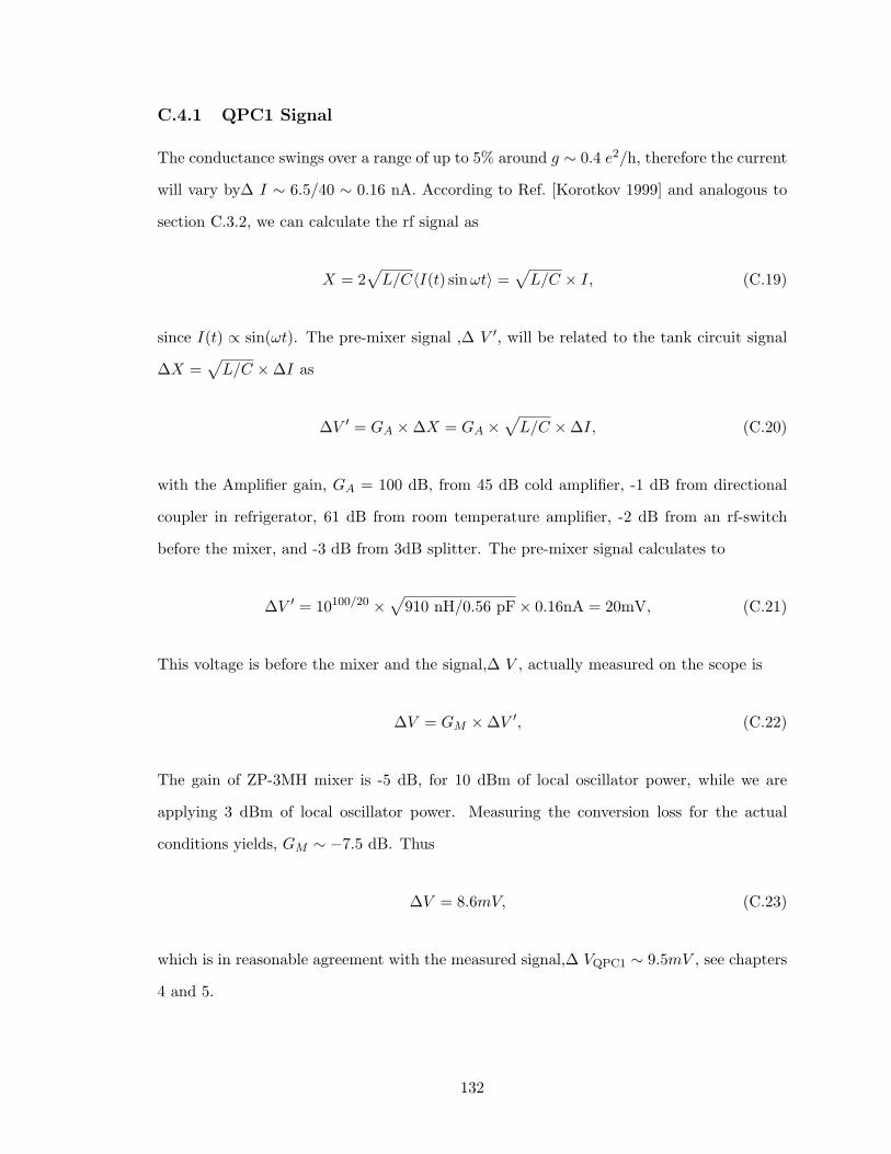
C.4.1 QPC1 Signal
The conductance swings over a range of up to 5% around g ∼ 0.4 e2/h, therefore the current
will vary by∆ I ∼ 6.5/40 ∼ 0.16 nA. According to Ref. [Korotkov 1999] and analogous to
section C.3.2, we can calculate the rf signal as
X = 2
L/CI(t) sinωt =
L/C × I, (C.19)
since I(t) ∝ sin(ωt). The pre-mixer signal ,∆ V , will be related to the tank circuit signal
∆X =
L/C ×∆I as
∆V = GA ×∆X = GA ×
L/C ×∆I, (C.20)
with the Amplifier gain, GA = 100 dB, from 45 dB cold amplifier, -1 dB from directional
coupler in refrigerator, 61 dB from room temperature amplifier, -2 dB from an rf-switch
before the mixer, and -3 dB from 3dB splitter. The pre-mixer signal calculates to
∆V = 10100/20 ×
910 nH/0.56 pF× 0.16nA = 20mV, (C.21)
This voltage is before the mixer and the signal,∆ V , actually measured on the scope is
∆V = GM ×∆V , (C.22)
The gain of ZP-3MH mixer is -5 dB, for 10 dBm of local oscillator power, while we are
applying 3 dBm of local oscillator power. Measuring the conversion loss for the actual
conditions yields, GM ∼ −7.5 dB. Thus
∆V = 8.6mV, (C.23)
which is in reasonable agreement with the measured signal,∆ VQPC1 ∼ 9.5mV , see chapters
4 and 5.
132
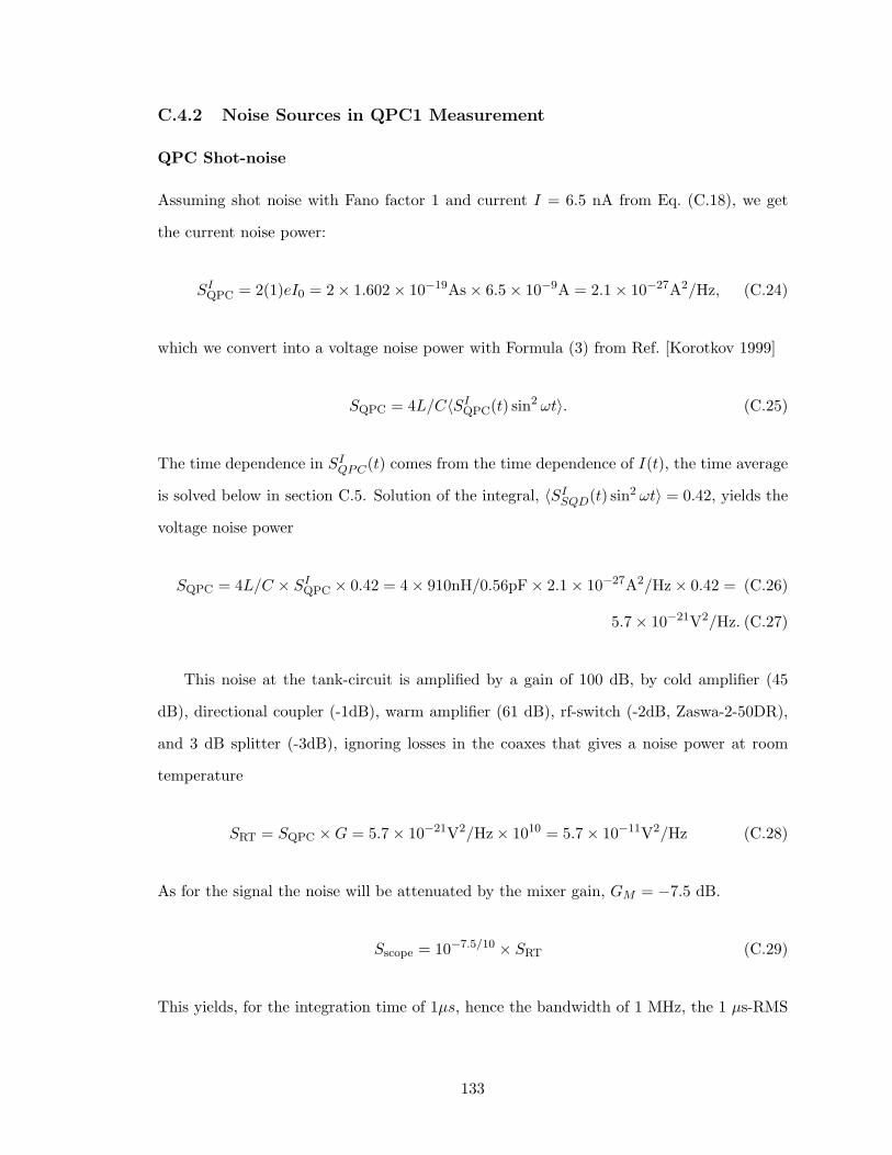
C.4.2 Noise Sources in QPC1 Measurement
QPC Shot-noise
Assuming shot noise with Fano factor 1 and current I = 6.5 nA from Eq. (C.18), we get
the current noise power:
SIQPC = 2(1)eI0 = 2× 1.602× 10−19As× 6.5× 10−9A = 2.1× 10⁻²⁷A2/Hz, (C.24)
which we convert into a voltage noise power with Formula (3) from Ref. [Korotkov 1999]
SQPC = 4L/CSIQPC(t) sin2 ωt. (C.25)
The time dependence in SIQPC(t) comes from the time dependence of I(t), the time average
is solved below in section C.5. Solution of the integral, SISQD(t) sin2 ωt = 0.42, yields the
voltage noise power
SQPC = 4L/C × SIQPC × 0.42 = 4× 910nH/0.56pF× 2.1× 10−27A2/Hz× 0.42 = (C.26)
5.7× 10⁻²¹V2/Hz. (C.27)
This noise at the tank-circuit is amplified by a gain of 100 dB, by cold amplifier (45
dB), directional coupler (-1dB), warm amplifier (61 dB), rf-switch (-2dB, Zaswa-2-50DR),
and 3 dB splitter (-3dB), ignoring losses in the coaxes that gives a noise power at room
temperature
SRT = SQPC ×G = 5.7× 10⁻²¹V2/Hz× 1010 = 5.7× 10⁻¹¹V2/Hz (C.28)
As for the signal the noise will be attenuated by the mixer gain, GM = −7.5 dB.
Sscope = 10−7.5/10 × SRT (C.29)
This yields, for the integration time of 1µs, hence the bandwidth of 1 MHz, the 1 µs-RMS
133
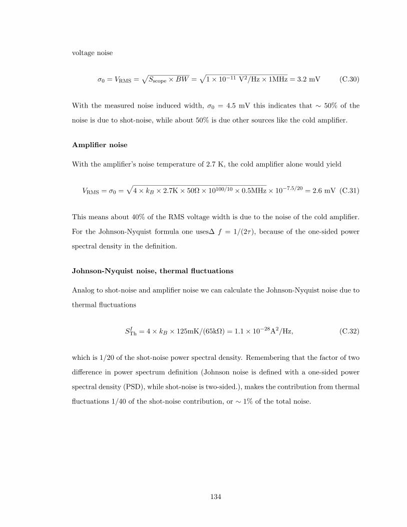
voltage noise
σ0 = VRMS =
Sscope ×BW =
1× 10⁻¹¹ V2/Hz× 1MHz = 3.2 mV (C.30)
With the measured noise induced width, σ0 = 4.5 mV this indicates that ∼ 50% of the
noise is due to shot-noise, while about 50% is due other sources like the cold amplifier.
Amplifier noise
With the amplifier’s noise temperature of 2.7 K, the cold amplifier alone would yield
VRMS = σ0 =
4× kB × 2.7K× 50Ω× 10100/10 × 0.5MHz× 10−7.5/20 = 2.6 mV (C.31)
This means about 40% of the RMS voltage width is due to the noise of the cold amplifier.
For the Johnson-Nyquist formula one uses∆ f = 1/(2τ), because of the one-sided power
spectral density in the definition.
Johnson-Nyquist noise, thermal fluctuations
Analog to shot-noise and amplifier noise we can calculate the Johnson-Nyquist noise due to
thermal fluctuations
SITh = 4× kB × 125mK/(65kΩ) = 1.1× 10⁻²⁸A2/Hz, (C.32)
which is 1/20 of the shot-noise power spectral density. Remembering that the factor of two
difference in power spectrum definition (Johnson noise is defined with a one-sided power
spectral density (PSD), while shot-noise is two-sided.), makes the contribution from thermal
fluctuations 1/40 of the shot-noise contribution, or ∼ 1% of the total noise.
134
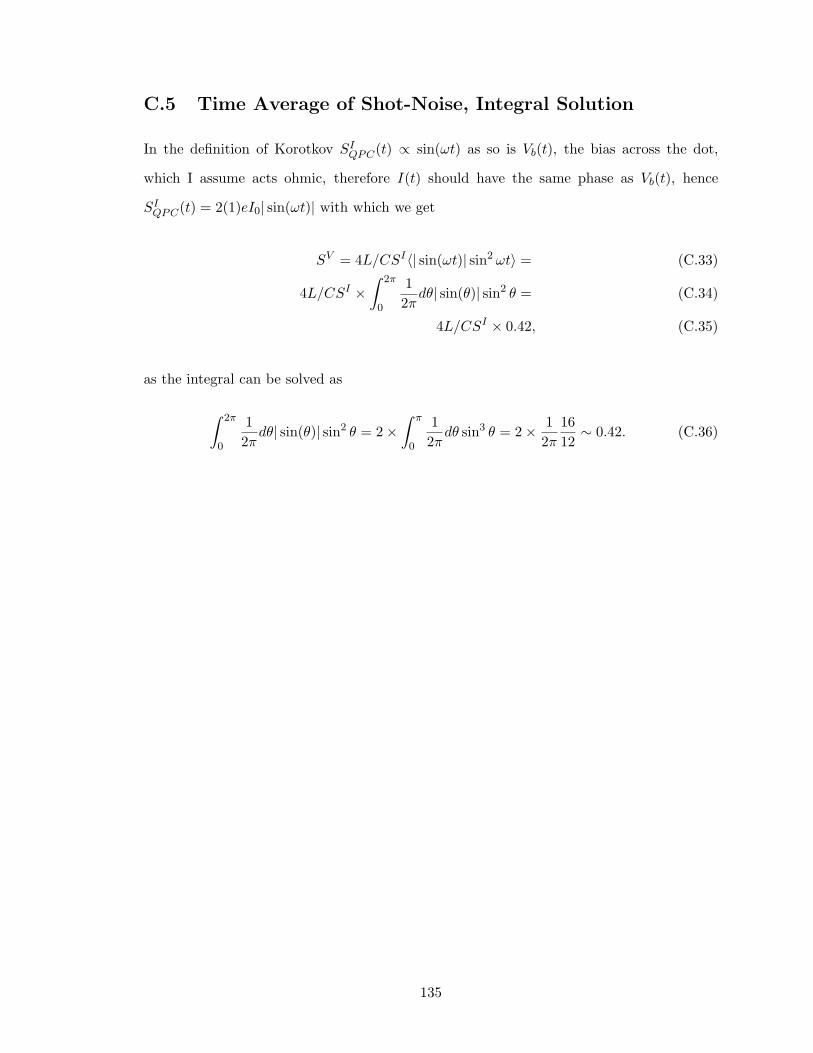
C.5 Time Average of Shot-Noise, Integral Solution
In the definition of Korotkov SIQPC(t) ∝ sin(ωt) as so is Vb(t), the bias across the dot,
which I assume acts ohmic, therefore I(t) should have the same phase as Vb(t), hence
SIQPC(t) = 2(1)eI0| sin(ωt)| with which we get
SV = 4L/CSI| sin(ωt)| sin2 ωt = (C.33)
4L/CSI × 2π
0
12π
dθ| sin(θ)| sin2 θ = (C.34)
4L/CSI × 0.42, (C.35)
as the integral can be solved as
2π
0
12π
dθ| sin(θ)| sin2 θ = 2× π
0
12π
dθ sin3 θ = 2× 12π
1612∼ 0.42. (C.36)
135
Appendix D
Rapid Single-Shot Measurement ofa Singlet-Triplet Qubit:Supplementary Material
C. Barthel1 D. J. Reilly1,2 C. M. Marcus1 M. P. Hanson3 A. C. Gossard3
1Department of Physics, Harvard University, 17 Oxford Street, Cambridge, Massachusetts
02138, USA
2School of Physics, University of Sydney, Sydney, 2006, Australia
3Materials Department, University of California, Santa Barbara, California 93106, USA
This supplementary note presents a derivation of an equation that appears in the main
text of the Letter “Rapid Single-Shot Measurement of a Singlet-Triplet Qubit” for the
ensemble-averaged triplet T+ return probability, PT . The equation is used to fit experimen-
tal data in Fig. 4(b) of that Letter. The analysis assumes classical Overhauser fields that
are static on the time scale of electron spin evolution but fluctuate randomly on longer time
scales, where ensemble statistics are measured.
136
In one of the experiments described in the accompanying Letter, “Rapid Single-Shot
Measurement of a Singlet-Triplet Qubit”, two electrons in a double quantum dot are ini-
tialized in the singlet state, then brought to the anticrossing of the lower branch of the
hybridized singlet, S, and the m = +1 triplet, T+ = |↑↑ . The hyperfine interaction felt
by the electrons due to the large number (∼ 106) of nuclei in the host material is treated
as an effective classical Zeeman (Overhauser) field acting on the electrons. The Overhauser
field is further assumed to be static on time scales of the electron dynamics. Near the
S − T+ resonance, the difference in transverse components of the Overhauser fields in the
left (L) and right (R) dots,∆ Bx(y) = [BLx(y) − BR
x(y)]/2 mix singlet and triplet state, while
the average longitudinal Overhauser field, Bz = [BLz + BR
z ]/2, acts as a random energy
detuning. An external magnetic field, B, defines the quantization axis z. This supple-
mentary note presents a derivation of the triplet probability, PT , used to fit experimental
data in Fig. 4(b), following Ref. [Taylor Thesis 2007]. The Hamiltonian in the basis (S, T+)
is [Coish 2005; Taylor PRB 2007]
H = g∗µB
−J/(g∗µB) cos θ B+/
√2
cos θ B−/√
2 B + Bz
, (D.1)
where cos θ is the (1,1) component of the hybridized singlet ground state, |S = cos θ |(1, 1)S+
sin θ |(0, 2)S and B± = ∆Bx ± i∆By. The effective electron g-factor is g∗ = −0.44. An
additional factor√
2 in the numerator of the off-diagonal term stems from constructive
interference of two electron spin flip - pathways, since there are two electrons participat-
ing [Coish 2005]. The exchange, J , the external magnetic field, B, and the nuclear Over-
hauser z-component, Bz, are combined to the energy mismatch δ = −g∗µB(B + Bz) − J .
In the described experiment the exchange is tuned to resonance, leaving δ = −g∗µBBz.
For an initial singlet cT (τI = 0) = 0 the solution for the probability amplitude, cT (τI),
is [CohenTanuoudji 1999]
cT (τI) =cos θ(∆Bx + i∆By)√
2 ω/|g∗µB|sin(ωτI), (D.2)
137
with the precession frequency, ω,
ω =12
δ2 + 2 cos2 θ (g∗µB)2(∆B2
x + ∆B2y) =
|g∗µB|2
B2
z + 2 cos2 θ (∆B2x + ∆B2
y).(D.3)
The nuclear Overhauser field z-component, Bz, and the gradient fields,∆ Bx and∆ By,
are not known and constant, but distributed [Coish 2005; Taylor PRB 2007] according to
the distribution function ρ(B) = (2πBnuc)−3/2e−(B/(Bnuc))2/2, with B = ( ∆Bx,∆By, Bz).
The evolution of the nuclear fields is slower than the evolution of the electron spin, hence
the triplet probability for an ensemble of measurements, P idealT (τI), can be written as the
integral of all probabilities for a single constant Overhauser field, weighted by ρ(B),
P idealT (τI) =
d3B ρ(B)cT (τI)c∗T (τI) =
d3B ρ(B)
cos2 θ (∆B2x + ∆B2
y)2 (ω/|g∗µB|)2 sin2(ωτI). (D.4)
The evolution occurs far detuned from the (1,1)-(0,2) charge degeneracy, therefore the
hybridized singlet is approximately identical to the (1,1) singlet, and cos θ ∼ 1. Furthermore
allowing an offset, P 0T , of PT , because of imperfect preparation or miscounting of singlets
as triplets and a smaller than one visiblity, V , yields the equation in the paper:
PT = P 0T + V
d3B ρ(B)
(∆B2x + ∆By)2
2 (ω/|g∗µB|)2 sin2(ωτI), (D.5)
which describes the measured triplet probability, averaged over many singleshot measure-
ments.
138
Appendix E
Dephasing due to Imperfect GateVoltage Pulses: SupplementaryMaterial to Chapter 7
C. Barthel1 J. M. Medford1 C. M. Marcus1 1Department of Physics, Harvard University,
17 Oxford Street, Cambridge, Massachusetts 02138, USA
This supplementary note presents a discussion of the influence of pulse-imperfections
on the envelope function of spin echo recovery amplitudes. For a constant gate-voltage
difference between the dephasing and rephasing step, before and after the π-pulse, inho-
mogenous broadening results in a Gaussian envelope function of the echo amplitude with a
microsecond time-scale. For a linear voltage droop over the whole time spent at the electron
separation point S, an envelope function of the form e−(τ/T ∗2,eff)4 is found. The analysis as-
sumes classical Overhauser fields that are static on the time scale of electron spin evolution
but fluctuate randomly on longer time scales, where ensemble statistics are measured. The
inhomogenous width T ∗2,eff would be fitted as and interpreted with an T2.
139
In one of the experiments described in chapter 7 of this thesis two electrons in a double
quantum dot are initialized in the separated singlet state, (1, 1)S. After a time τD/2 a
Hahn spin echo is performed and the singlet probability is measured after an additional
time τD/2, spent at point S. The hyperfine interaction felt by the electrons due to the large
number (∼ 106) of nuclei in the host material is treated as an effective classical Zeeman
(Overhauser) field acting on the electrons. The Overhauser field is further assumed to be
static on time scales of the electron dynamics. The longitudinal Overhauser field difference,
∆Bz = [BLz −BR
z ], acts as a random dephasing. An external magnetic field, B, defines the
quantization axis z.
E.1 Free Induction Decay
First we investigate the effect of a gate voltage drift during two-electron separation on the
free induction decay measurement that yields the inhomogeneous dephasing time T ∗2 , see
Ref. [Petta 2005]. Following Ref. [Taylor PRB 2007; Merkulov 2002] we can write down the
singlet return probability for a FID pulse in a constant field difference:
PS = cos2 (∆Bzγe/2τS) =12(1 + cos (∆BzγeτS)), (E.1)
where τS is the time the singlet spends separated in two dots. We can generalize this for a
field gradient that is not constant during the separation time:
PS = cos2 (γe/2 τS
0∆Bz(t)dt), (E.2)
with a time-dependent∆ Bz(t), due to a shift of the electron wavefunction over time induced
by a voltage-drift or -droop∆ V (t) of the double dot gate voltage detuning. Then the singlet
measurement probability becomes
PS = cos2 (γe/2 τS
0∆B0
z +d(∆Bz)d(∆V )
∆V (t)dt), (E.3)
140
with the change in gradient due to gate voltage change d(∆Bz)d(∆V ) . Assuming in first order,
that the nuclear field gradient is linear, and that the voltage droop is linear, we get
PS = cos2 (γe/2 [ ∆B0z +
d(∆Bz)d(∆V )
∆V τS]τS). (E.4)
Due to the assumption of a linear gradient, and linear voltage droop we can simplify
d(∆Bz)d(∆V )
=∆B0
z
aS
da
d∆V, (E.5)
with the two-electron separation, aS at the beginning of the separation, and the change
of separation dad∆V with gate voltage, assumed to be constant. This allows us to simplify
Eq. (E.4) to
PS = cos2 (γe/2 [1 +da
d∆V
∆V
aSτS]∆B0
z τS). (E.6)
which is identical to the regular free precession amplitude, aside from a small correction
dad∆V
∆VaS
. The inhomogenous broadening is dominated by the∆ B0z τS term.
E.2 Hahn Echo
For a Hahn echo, the evolution of the qubit is inverted after half of the total dephasing
time, τD, spent at the separation point. The singlet measurement probability for perfect
pulses and static nuclear field becomes:
PS = cos2 (∆Bzγe/2[τD/2− τD/2]), (E.7)
which is unity for arbitrary τD. The minus sign between the two times τD/2 is due to the
inversion of the evolution by the π-pulse.
E.2.1 Constant Offset between Gate Voltage Pulses
For a constant difference in gate voltage,∆ V , between the dephasing time window before
and the rephasing time window after the π-pulse we can modify the expression for an ideal
141
Hahn echo (E.7),
PS = cos2 (γe/2 [ ∆BzτD/2− (∆Bz + δ∆Bz) τD/2]), (E.8)
with the discrepancy in field difference, δ∆Bz, before and after the echo pulse. Due to the
field discrepancy only part of the dephasing will be refocussed,
PS = cos2 (γe/2 [−δ∆BzτD/2]) = cos2 (γeδ∆BzτD/4). (E.9)
The field discrepancy can be estimated from the relative shift in electron wave function due
to the voltage discrepancy.
δ∆Bz = ∆BzδaS
aS, (E.10)
with aS, the typical distance of the two electrons when separated into two dots, at point S,
and δaS, the difference in distance between the time interval before and after the π-pulse.
The electron wavefunction shift can be estimated from discrepancy, δ∆V , in gate voltage,
∆V , before and after the π-pulse,
δaS
aS= ∆Bz
daS
d∆V
1aS
δ∆V. (E.11)
Using the relation from Ref. [Taylor PRB 2007],
cos2 (ω τ) =12
1 + e−(t/T ∗2 )2
, (E.12)
we get:
PS =12
1 + e−(t/T ∗2,eff)2
, (E.13)
with the effective T ∗2 ,
T ∗2,eff = 2T ∗
2aS
δaS, (E.14)
142
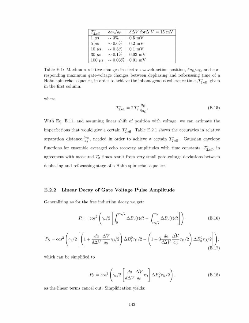
T ∗2,eff δaS/aS δ∆V for∆ V = 15 mV
1 µs ∼ 3% 0.5 mV5 µs ∼ 0.6% 0.2 mV10 µs ∼ 0.3% 0.1 mV30 µs ∼ 0.1% 0.03 mV100 µs ∼ 0.03% 0.01 mV
Table E.1: Maximum relative changes in electron-wavefunction position, δaS/aS, and cor-responding maximum gate-voltage changes between dephasing and refocussing time of aHahn spin echo sequence, in order to achieve the inhomogenous coherence time ,T ∗
2,eff , givenin the first column.
where
T ∗2,eff = 2T ∗
2aS
δaS, (E.15)
With Eq. E.11, and assuming linear shift of position with voltage, we can estimate the
imperfections that would give a certain T ∗2,eff . Table E.2.1 shows the accuracies in relative
separation distance, δaSaS
, needed in order to achieve a certain T ∗2,eff . Gaussian envelope
functions for ensemble averaged echo recovery amplitudes with time constants, T ∗2,eff , in
agreement with measured T2 times result from very small gate-voltage deviations between
dephasing and refocussing stage of a Hahn spin echo sequence.
E.2.2 Linear Decay of Gate Voltage Pulse Amplitude
Generalizing as for the free induction decay we get:
PS = cos2
γe/2
τD/2
0∆Bz(t)dt−
τD
τD/2∆Bz(t)dt
, (E.16)
PS = cos2
γe/2
1 +
da
d∆V
∆V
aSτD/2
∆B0
z τD/2−
1 + 3da
d∆V
∆V
aSτD/2
∆B0
z τD/2
,
(E.17)
which can be simplified to
PS = cos2
γe/2
da
d∆V
∆V
aSτD
∆B0
z τD/2
, (E.18)
as the linear terms cancel out. Simplification yields:
143
PS = cos2
γe/4
da
d∆V
∆V
aS
∆B0
z τ2D
, (E.19)
Using the relation from Ref. [Taylor PRB 2007],
cos2 (ω τ) =12
1 + e−(t/T ∗2 )2
, (E.20)
we get:
PS =12
1 + e−(t/T ∗2,eff)4
, (E.21)
with an effective T ∗2 ,
(T ∗2,eff)2 = 2T ∗
2
da
d∆V
∆V
aS
−1
. (E.22)
The term in the brackets can be identified as the time it takes for the electrons to drift back
into on dot, which is roughly ∼ 100 µs. Therefore (T ∗2,eff) ∼ 2 µs for our dots without any
compensation.
Acknowledgements
The inhomogeneous broadening effect and the idea for its derivation was pointed out to us by
Hendrik Bluhm, to whom we are especially grateful for useful discussion. We acknowledge
funding from ARO/iARPA, the Department of Defense. This work was performed in part
at the Center for Nanoscale Systems (CNS), a member of the National Nanotechnology
Infrastructure Network (NNIN), which is supported by the National Science Foundation
under NSF award no. ECS-0335765. We thank Sandra Foletti, David Reilly and W. Witzel,
for useful discussion.
144
Appendix F
Etched Structures to define GaAsQuantum Dots
F.1 Motivation
Much progress has been made in the realization of almost all the requirements for a vi-
able singlet-triplet qubit for quantum information processing [DiVincenzo 1998]. Single-
qubit initialization, universal control, fast measurement and coherence have been demon-
strated, see chapter 2. Two-qubit operations are crucial for the implementation of quan-
tum computing. In order to couple two singlet-triplet qubits, at least two double quan-
tum dots need to be fabricated in close vicinity to allow charge coupling between the
two [Taylor 2006; Laird 2010]. Two-qubit operations using dot-dot tunnel coupling is also
thinkable and needs two double dots in close vicinity as well.
Depletion gates are a versatile tool for the confinement of double and multiple quantum
dots. The need to contact them bears complications for large numbers of devices though
because not only the depletion gates themselves need to be intregrated in tight space, con-
nector layers run across the whole mesa and need ∼ 100 µm sized bond pads. Furthermore,
a large number of metallic gates screens the electrical interaction between the electrons in
for example two double dots. Creating confinement without metallic gates, e.g. by etch-
ing features into a GaAs heterostructure may thus be a useful tool to be combined with
depletion gates to create multiple charge and tunnel coupled quantum dots in close vicinity.
145
F.2 Etched Lines, Widths and Depths
Reactive ion beam etching when applied to a GaAs heterostructure surface, can etch narrow
trenches into the material and thus remove the Si delta-dopant layer, thereby completely
depleting the 2DEG underneath. With this in mind, trenches were written using a reactive
ion etch, to test the feasibility and the achievable smallest feature size. The work was
performed on the RIE7 - Unaxis Shuttleline ICP RIE, an Inductive Coupled Plasma reactor.
85-90 degree side wall angles, sharp edges and smooth etched surface
E-beam dose: 300 uC/cm^2E-beam dose: 325 uC/cm^2
85-90 degree side wall angles, well etched
E-beam dose: 425 uC/cm^2
“V” shape cross section
Richard Schalek measured the depth and width of some of trenches using AFM.The results are shown in Figs. 1 & 2. As a comparison, the line width measured with SEM is presented in Fig. 3, indicating the results are quite different. AFM data is greater than SEM data.
0
50
100
150
200
275 325 375 425 475
E-beam Dose (uC/cm^2)
Etch
Dep
th (n
m)
Left line
50 nm
80 nm
110 nm
050
100150
200250
300
275 325 375 425 475
E-beam dose (uC/cm^2)
Line
wid
th (n
m)
left line
50 nm
80 nm
110 nm
020406080
100120140160180200
250 350 450 550
e-beam dosage (uC/cm^2)
Line
wid
th m
easu
red
(nm
) 30405060708090100110120
Design line width (nm)
Fig. 1 AFM etch depth vs. doses
Fig. 2 AFM trench width vs. doses Fig. 3 SEM trench width vs. doses
Design line width
Design line width
(a) (b)
(c)(d)
Figure F.1: (a) Scanning electron beam images of cross section of GaAs wafer with trenchesetched by reactive ion etching. The e-beam dosage is 300 µC/cm2, the design line widthsare 120 nm for the right line, decreasing by 10 nm for each line towards the left. Lines fordesign line widths of 30, 40 nm are not visible. (b) Identical to (a) but with e-beam doseof 325 µC/cm2. (c) Identical to (a) but with e-beam dose of 425 µC/cm2. The trenchestake a wedge shape and are much wider and deeper than intended. (d) Trench widths foretched heterostructures as shown in (a)-(c), as a function of e-beam dosage, for differentdesign trench widths.
Features, defined by e-beam resist, down to 60 nm width can be written and etch depths
146
of ∼ 100 nm, sufficient for dopant-layer removal for most heterostructures, can be achieved.
Etch-depth weakly depends on dose, but strongly on design width. For design widths of
∼ 50 nm the etch-depth is ∼ 100 nm, while the etch depth for ∼ 100 nm design width is
∼ 200 nm.
SEM images of cross sections of etched trenches are shown in Fig. F.1(a)-(c) for three
different e-beam dosages. For the lowest dosage, 300 µC/cm2, the trenches are not fully
etched, while for higher doses the trenches become much deeper and wider than intended
and wedge-shaped. For ∼ 325, µC/cm2, see Fig. F.1(b) an optimal line depth (∼ 100 nm)
and width [∼ 60 nm, see Fig. F.1(c)] are obtained.
Acknowledgements
The work in this appendix was done in collaboration with Colin Dillard and Ling Xie. Ling
Xie performed the etch in the cleanroom at the Center for Nanoscale Systems (CNS), a mem-
ber of the National Nanotechnology Infrastructure Network (NNIN), which is supported by
the National Science Foundation under NSF award no. ECS-0335765.
147
Bibliography
[Aharonov 1988] Y. Aharonov, D.Z. Albert, and L. Vaidman, How the result of a measure-
ment of a component of the spin of a spin-1/2 particle can turn out to be 100,
Phys. Rev. Lett. 60, 1351 (1988).
[Amasha 2008] S. , K. MacLean, I. P. Radu, D. M. Zumbuhl, M. Kastner, M. P. Han-
son, and A. C. Gossard, Electrical Control of Spin Relaxation in a Quantum Dot
Phys. Rev. Lett. 100, 046803(2008).
[Armen 2002] M. A. Armen et al., Adaptive Homodyne Measurement of Optical Phase,
Phys. Rev. Lett. 89, 133602 (2002).
[Astafiev 2004] O. Astaev et al., Single-shot measurement of the Josephson charge qubit,
Phys. Rev. B 69, 180507 (2004).
[Barnenco 1995] A. Barenco, A universal 2-bit gate for quantum computation, P. Roy. Soc.
Lond. A-Mat. 449, 679 (1995).
[Barthel 2009] C. Barthel, D. J. Reilly, C. M. Marcus, M. P. Hanson, and A. C. Gossard,
Rapid single-shot measurement of a singlet-triplet qubit, Phys. Rev. Lett. 103,
160503 (2009).
[Barthel SQD 2010] C. Barthel, M. Kjærgaard, J. Medford, M., M. Stopa, C. M. Marcus,
M. P. Hanson, and A. C. Gossard, Fast sensing of double-dot charge arrangement
and spin state with an rf sensor quantum dot, Phys. Rev. B 81, 161308(R) (2010).
[Barthel T1 2010] C. Barthel, J. Medford, H. Bluhm, C. M. Marcus, M. P. Hanson, and
148
A. C. Gossard, Singlet-Triplet Qubit Relaxation and Initialization in a Magnetic
Field Gradient, in preparation(2010).
[Barthel T2 2010] C. Barthel, J. Medford, C. M. Marcus, M. P. Hanson, and A. C. Gossard,
Dynamic Decoupling and Protected Coherent Operations of a Singlet Triplet Qubit,
in preparation (2010).
[Baugh 2007] J. Baugh, Y. Kitamura, K. Ono, and S. Tarucha, Large nuclear overhauser
fields detected in vertically coupled double quantum dots, Phys. Rev. Lett. 99, 4
(2007).
[Beenakker Review 1991] C. W. J. Beenakker, H. van Houten Quantum Transport in Semi-
conductor Nanostructures Solid State Physics 44, 1 (1991).
[Beenakker CB 1991] C. W. J. Beenakker, Theory of Coulomb-blockade oscillations in the
conductance of a quantum dot Phys. Rev. B 44, 1646 (1991).
[Bell 1962] R. L. Bell, Electric dipole spin transitions in InSb, Phys. Rev. Lett. 9, 52 (1962).
[Bleany 1953] B. Bleaney, and K. W. H. Stevens, Paramagnetic resonance Rep. Prog. Phys.
16, 108 (1953)
[Bluhm FB 2010] H. Bluhm, S. Foletti, D. Mahalu, V. Umansky, and A. Yacoby, Enhanc-
ing the Coherence of Spin Qubits by Narrowing the Nuclear Spin Bath Using a
Quantum Feedback Loop, Phys. Rev. Lett., submitted (2010)
[Bluhm T2 2010] H. Bluhm, S. Foletti, I. Neder, M.Rudner, D. Mahalu, V. Umansky, and
A. Yacoby, Long coherence of electron spins coupled to a nuclear spin bath, Nature
Physics, submitted (2010)
[Buehler 2005] T. M. Buehler, D. J.Reilly, R. P. Starrett, A. D. Greentree, A. R. Hamilton,
A. S. Dzurak, and R. G. Clark, Single-shot readout with the radio-frequency single-
electron transistor in the presence of charge noise, Appl. Phys. Lett. 86 143117
(2005).
149
[Buizert 2008] C. Buizert, F. H. L. Koppens, M. Pioro-Ladriere, H.-P. Tranitz, I. T. Vink,
S. Tarucha, W. Wegscheider, and L. M. K. Vandersypen, In situ reduction of
charge noise in GaAs/AlxGa1−xAs Schottky-gated devices, Phys. Rev. Lett. 101,
1 (2008).
[Carr 1954] H. Y. Carr, E. M. Purcell, Effects of Diffusion on Free Precession in Nuclear
Magnetic Resonance Experiments, Phys. Rev. 94, 630638 (1954)
[Cassidy 2008] M. Cassidy, Effects of Diffusion on Free Precession in Nuclear Magnetic
Resonance Experiments, Master’s thesis, University of New South Wales (2008)
[CohenTanuoudji 1999] C.Cohen-Tannoudji, Quantum Mechanics 2, 4.3.3 (1999).
[Coish 2005] W. A. Coish, and D. Loss, Singlet-triplet decoherence due to nuclear spins in
a double quantum dot Phys. Rev. B,72, 125337,(2005).
[Cronenwett 2001] S. M. Cronenwett, Coherence, charging and spin effects in quantum dots
and point contacts, Ph.D. Thesis, Harvard University (2001).
[Das Sarma 2001] S. Das Sarma, Spintronics, Am. Sci. 89, 516 (2001).
[Datta 1990] S. Datta, and B. Das, Electronic analog of the electrooptic modulator, Appl.
Phys. Lett. 56, 665 (1990).
[De 2009] A. De, C. E. Pryor, and M. E. Flatte, Electric-field control of a hydrogenic donor’s
spin in a semiconductor, Phys. Rev. Lett. 102, 017603 (2009).
[Dicarlo 2004] L. Dicarlo, H. Lynch, A. C. Johnson, L. I. Childress, K. Crockett, C. M.
Marcus, M. Hanson, and A. C. Gossard, Differential charge sensing and charge
delocalization in a tunable double quantum dot, Phys. Rev. Lett. 92, 226801 (2004).
[Dicarlo Thesis 2007] L. Dicarlo, Mesoscopic Electronics Beyond DC Transport, Ph.D. The-
sis, Harvard University (2007).
[DiVincenzo 1995] D. P. DiVincenzo, 2-bit gates are universal for quantum computation,
Phys. Rev. A 51, 1015 (1995).
150
[DiVincenzo 1998] D. P. DiVincenzo, and D. Loss, Quantum information is physical, Su-
perlattices Microstruct. 23, 419 (1998).
[Dobers 1988] M. Dobers, K. V. Klitzing, J. Schneider, G. Weimann, and K. H. Ploog, Elec-
trical detection of nuclear magnetic-resonance in GaAs-AlxGa1−xAs heterostruc-
tures, Phys. Rev. Lett. 61, 1650 (1988).
[Drummond 1986] T. Drummond, W. T. Masselink, and H. Morcok, Modulation-doped
GaAs/(Al,Ga)As heterojunction field-effect transistors - modfets, P. Ieee 74, 773
(1986).
[Elzerman 2003] J. Elzerman, R. Hanson, J. S. Greidanus, L. H. W. V. Beveren, S. D.
Franceschi, L. M. K. Vandersypen, S. Tarucha, and L. P. Kouwenhoven, Few-
electron quantum dot circuit with integrated charge read out, Phys. Rev. B 67, 4
(2003).
[Elzerman 2004] J. M. Elzerman, R. Hanson, L. H. Willems van Beveren, B. Witkamp,
L. M. K. Vandersypen, and L. P. Kouwenhoven, Single-shot read-out of an indi-
vidual electron spin in a quantum dot, Nature 430, 431 (2004).
[Engel 2001] H.-A. Engel and D. Loss, Detection of single spin decoherence in a quantum
dot via charge currents, Phys. Rev. Lett. 86, 4648 (2001).
[Fermi 1930] E. Fermi, Uber die magnetischen Momente der Atomkerne. (About the mag-
netic moment of atomic nuclei.) Z. Phys.60, 320 (1930)
[Fertig 1987] H. Fertig, and B. I. Halperin, Transmission coefficient of an electron through
a saddle-point potential in a magnetic field Phys. Rev. B 36, 7969 (1987).
[38] R. Feynman, Simulating physics with computers, International Journal of Theo-
retical Physics 21, 467 (1982).
[Field 1993] M. Field, C. G. Smith, M. Pepper, D. A. Ritchie, J. E. F. Frost, G. A.
C. Jones, and D. G. Hasko, Measurements of Coulomb blockade with a noninvasive
voltage probe, Phys. Rev. Lett. 70, 1311 (1993).
151
[Foletti 2009] S. Foletti, H. Bluhm, D. Mahalu, V. Umansky, and A. Yacoby, Universal
quantum control of two-electron spin quantum bits using dynamic nuclear polar-
ization, Nature physics, 5, 903 (2009)
[Franken 1961] P. Franken, G. Weinreich, C. Peters, and A. Hill, Generation of optical
harmonics, Phys. Rev. Lett. 7, 118 (1961).
[Fujisawa 1998] T. Fujisawa, T. H. Oosterkamp, W. G. van der Wiel, B. W. Broer,
R. Aguado, S. Tarucha, and L. P. Kouwenhoven, Spontaneous Emission Spectrum
in Double Quantum Dot Devices, Science 282, 932 (1998).
[Fujisawa 2004] T. Fujisawa, T. Hayashi, Y. Hirayamab, H. D. Cheong, and Y. H. Jeong,
Real-time detection of single-electron tunneling current Appl. Phys. Lett. 84, 2343
(2004).
[Goldhaber-Gordon 1998] D. Goldhaber-Gordon, H. Shtrikman, D. Mahalu, D. Abusch-
Magder, U. Meirav, and M. Kastner, Kondo effect in a single-electron transistor,
Nature 391, 156 (1998).
[Golovach 2006] V. N. Golovach, M. Borhani and D. Loss, Electric-dipole-induced spin res-
onance in quantum dots, Phys. Rev. B, 74 165319 (2006)
[Grover 1997] L. Grover, Quantum mechanics helps in searching for a needle in a haystack,
Phys. Rev. Lett. 79, 325 (1997).
[Gueron 1959] M. Gueron and C. Ryter, Overhauser effect in metallic lithium, Phys. Rev.
Lett. 3, 338 (1959).
[Gulland 2010] M. Gulland, J. J. Krich, J. M. Taylor, H. Bluhm, B. I. Halperin, C. M. Mar-
cus, M. Stopa, A. Yacoby, and M. D. Lukin, Dynamic Nuclear Polarization in
Double Quantum Dots arXiv: 1003.4508v1 (2010)
[Hahn 1950] E. L. Hahn, Spin Echoes, Phys. Rev. 80, 580 (1950)
[Hanson 2003] R. Hanson, B. Witkamp, L. M. K. Vandersypen, L. H. W. V. Beveren,
152
J. Elzerman, and L. P. Kouwenhoven, Zeeman energy and spin relaxation in a
one-electron quantum dot, Phys. Rev. Lett. 91, 196802 (2003).
[Hanson 2007] R. Hanson, L. P. Kouwenhoven, J. R. Petta, S. Tarucha, and L. M. K. Van-
dersypen, Spins in few-electron quantum dots, Rev. Mod. Phys. 79, 1217 (2007).
[Horowitz 1989] P. Horowitz, and W. Hill, The art of electronics, Cambridge University
Press, 2 edition (1989)
[Ihn 2009] T. Ihn, S. Gustavsson, U. Gasser, B. Kung, T. Muller, R. Schleser, M. Sigrist,
I. Shorubalko, R. Leturcq, and K. Ensslin, Quantum dots investigated with charge
detection techniques Solid State Communications 149, 1419-1426 (2009).
[Jelezko 2004] F. Jelezko, T. Gaebel, I. Popa, A. Gruber, and J. Wrachtrup, Observation of
coherent oscillations in a single electron spin, Phys. Rev. Lett. 92, 076401 (2004).
[Johnson Nature 2005] A. C. Johnson, J. R. Petta, J. M Taylor, A. Yacoby, M. D. Lukin,
C. M. Marcus, M. Hanson, and A. C. Gossard, Triplet-singlet spin relaxation via
nuclei in a double quantum dot, Nature 435, 925 (2005).
[Johnson PRB 2005] A. C. Johnson, J. R. Petta, and C. M. Marcus, Singlet-triplet spin
blockade and charge sensing in a few-electron double quantum dot, Phys. Rev. B
72, 7 (2005).
[Johnson Thesis 2005] A. C. Johnson, Charge sensing and spin dynamics in GaAs quantum
dots, Ph.D. Thesis, Harvard University (2005).
[Kato 2003] Y. Kato, R. Myers, D. C. Driscoll, A. C. Gossard, J. Levy, and D. Awschalom,
Gigahertz electron spin manipulation using voltage-controlled g-tensor modulation,
Science 299, 1201 (2003).
[Katz 2008] N. Katz, M. Neeley, M. Ansmann, R. C. Bialczak, M. Hofheinz, E. Lucero,
A. O’Connell, H. Wang, A. N. Cleland, J. M. Martinis, and A. N. Korotkov,
Reversal of the weak measurement of a quantum state in a superconducting phase
qubit, Phys. Rev. Lett. 101, 200401 (2008).
153
[Khaetski 2002] A. Khaetskii, D. Loss, and L. Glazman, Electron spin decoherence in quan-
tum dots due to interaction with nuclei, Phys. Rev. Lett. 88, 186802 (2002).
[Khazan 1993] L. Khazan, Y. Rubo, and V. Sheka, Exchange-induced optical spin transi-
tions in semimagnetic semiconductors, Phys Rev B 47, 13180 (1993).
[Kitaev 1997] A. Kitaev, Quantum computations: algorithms and error correction, Russ.
Math. Surv. 52, 1191 (1997).
[Koppens 2005] F. H. L. Koppens, J. A. Folk, J. Elzerman, R. Hanson, L. H. W. V. Beveren,
I. T. Vink, H.-P. Tranitz, W. Wegscheider, L. P. Kouwenhoven, and L. M. K.
Vandersypen, Control and detection of singlet-triplet mixing in a random nuclear
field, Science 309, 1346 (2005).
[Koppens 2006] F. H. L. Koppens, C. Buizert, K. J. Tielrooij, I. T. Vink, K. C. Nowack,
T. Meunier, L. P. Kouwenhoven, and L. M. K. Vandersypen, Driven coherent
oscillations of a single electron spin in a quantum dot, Nature 442, 766 (2006).
[Koppens 2007] F. H. L. Koppens, D. Klauser, W. A. Coish, K. C. Nowack, L. P. Kouwen-
hoven, D. Loss, and L. M. K. Vandersypen, Universal phase shift and nonexponen-
tial decay of driven single-spin oscillations, Phys. Rev. Lett. 99, 106803 (2007).
[Korotkov 1999] A. N. Korotkov, and M. A. Paalanen, Charge sensitivity of radio frequency
single-electron transistor Appl. Phys. Lett. 74, 4052 (1999).
[Kouwenhoven 1999] L. P. Kouwenhoven, C. M. Marcus, P. L. McEuen, S. Tarucha, R. M.
Westervelt, and N. S. Wingreen, Electron transport in quantum dots, in Mesoscopic
Electron Transport (Kluwer Academic, Dordrecht, 1997).
[Laird 2006] E. A. Laird, J. R. Petta, A. C. Johnson, C. M. Marcus, A. Yacoby, M. P.
Hanson, and A. C. Gossard, Effect of exchange interaction on spin dephasing in a
double quantum dot, Phys. Rev. Lett. 97, 4 (2006).
[Laird 2007] E. A. Laird, C. Barthel, E. I. Rashba, C. M. Marcus, M. P. Hanson, and A. C.
Gossard, Hyperfine-mediated gate-driven electron spin resonance, Phys. Rev. Lett.
99, 246601 (2007).
154
[Laird 2009] E. A. Laird, C. Barthel, E. I. Rashba, C. M. Marcus, M. P. Hanson, and A. C.
Gossard, A new mechanism of electric dipole spin resonance: hyperfine coupling
in quantum dots, Semicond. Sci. Technol. 24, 064004 (2009).
[Laird 2010] E. A. Laird, Electrical control of quantum dot spin qubits Ph.D. Thesis, Har-
vard University
[Lee 2008] B. Lee, W. M. Witzel, and S. Das Sarma Universal Pulse Sequence to Minimize
Spin Dephasing in the Central Spin Decoherence Problem Phys. Rev. Lett. 100,
160505 (2008)
[Levitov 2003] L. S. Levitov and E. I. Rashba, Dynamical spin-electric coupling in a quan-
tum dot, Phys. Rev. B 67, 5 (2003).
[Levy 2002] J. Levy, Universal quantum computation with spin-1/2 pairs and Heisenberg
exchange, Phys. Rev. Lett. 89, 147902 (2002).
[Loss 1998] D. Loss, and D.P. DiVincenzo, Quantum computation with quantum dots, Phys.
Rev. A 57 589 (1998).
[Lu 2003] W. Lu, Z. Ji, L. Pfeiffer, K. W. West, and A. J. Rimberg, Real-time detection of
electron tunneling in a quantum dot, Nature 423 422 (2003).
[McCombe 1967] B. McCombe, S. Bishop, and R. Kaplan, Combined resonance and electron
g-values in InSb, Phys. Rev. Lett. 18, 748 (1967).
[Meiboom 1958] S. Meiboom, D. Gill, Modified Spin-Echo Method for Measuring Nuclear
Relaxation Times Rev. Sci. Instrum. 29, 688 (1958)
[Merkulov 2002] Merkulov I A, Efros Al L and Rosen M Electron spin relaxation by nuclei
in semiconductor quantum dots, Phys. Rev. B, 65 205309 (2002)
[Mermin 2007] N. D. Mermin, Quantum Computer Science Cambridge University Press,
2007.
[Meunier 2006] T. Meunier, I. Vink, L. H. Willems van Beveren, F. H. .L. Koppens, H.-
P. Tranitz, W. Wegscheider, L. P. Kouwenhoven, and L. M. K. Vandersypen,
155
Single-shot readout of electron spins in a semiconductor quantum dot Phys. Rev.
B 74, 195303 (2006).
[Monzon 1997] F. G. Monzon, M. Johnson, and M. L. Roukes, Strong Hall voltage modu-
lation in hybrid ferromagnet/semiconductor microstructures Appl. Phys. Lett. 71
(21), 3087 (1997)
[SETE code] The SETE code is available from the National Nanotechnology Infrastruc-
ture Network Computation project through the Harvard University Center for
Nanoscale Systems, www.cns.fas.harvard.edu.
[Nowack 2007] K. C. Nowack, F. H. L. Koppens, Y. V. Nazarov, and L. M. K. Vandersypen,
Coherent control of a single electron spin with electric fields, Science 318, 1430
(2007).
[Ono 2002] K. Ono, Current rectification by Pauli exclusion in a weakly coupled double
quantum dot system, Science 297, 1313 (2002).
[Ono 2004] K. Ono and S. Tarucha, Nuclear-spin-induced oscillatory current in spin-
blockaded quantum dots, Phys. Rev. Lett. 92, 256803 (2004).
[Overhauser 1953] A. Overhauser, Polarization of nuclei in metals, Phys. Rev. 91, 476
(1953).
[Paget 1977] D. Paget, G. Lampel, B. Sapoval, and V. Safarov, Low field electron-nuclear
spin coupling in gallium-arsenide under optical-pumping conditions, Phys. Rev. B
15, 5780 (1977).
[Pasini 2009] S. Pasini, G. S. Uhrig, Optimized dynamical decoupling for power-law noise
spectra Phys. Rev. A 81, 012309 (2010)
[Pauli 1925] W. Pauli, Uber den Zusammenhang des Abschlusses der Elektronengruppen
im Atom mit der Komplexstruktur der Spektren (On the Connexion between the
Completion of Electron Groups in an Atom with the Complex Structure of Spectra),
Z. Phys. 31, 765 (1925)
156
[Pekar 1965] S. I. Pekar and E. I. Rashba, Combined resonance in crystals in inhomogeneous
magnetic fields, Sov. Phys. - JETP 20, 1295 (1965).
[Petta 2004] J. R. Petta, A. C. Johnson, C. M. Marcus, M. Hanson, and A. C. Gossard,
Manipulation of a single charge in a double quantum dot, Phys. Rev. Lett. 93,
186802 (2004).
[Petta 2005] J. R. Petta, A. C. Johnson, J. M. Taylor, E. A. Laird, A. Yacoby, M. D. Lukin,
C. M. Marcus, M. P. Hanson, and A. C. Gossard, Coherent manipulation of coupled
electron spins in semiconductor quantum dots, Science 309, 2180 (2005).
[Petta PRB 2005] J. R. Petta, A. C. Johnson, A. Yacoby, C. M. Marcus, M. Hanson, and
A. C. Gossard, Pulsed-gate measurements of the singlet-triplet relaxation time in
a two-electron double quantum dot, Phys. Rev. B 72, 161301 (2005).
[Petta 2008] J. R. Petta, J. M Taylor, A. C. Johnson, A. Yacoby, M. D. Lukin, C. M. Mar-
cus, M. Hanson, and A. C. Gossard, Dynamic Nuclear Polarization with Single
Electron Spins, Phys. Rev. Lett. 100, 067601 (2008).
[Pioro-Ladriere 2007] M. Pioro-Ladriere, Y. Tokura, T. Obata, T. Kubo, and S. Tarucha,
Micromagnets for coherent control of spin-charge qubit in lateral quantum dots,
Appl. Phys. Lett. 90, 024105 (2007).
[Pioro-Ladriere 2008] M. Pioro-Ladriere, T. Obata, Y. Tokura, Y.-S. Shin, T. Kubo,
K. Yoshida, T. Taniyama, and S. Tarucha, Electrically driven single-electron spin
resonance in a slanting Zeeman field, Nature Physics 4, 776 (2008).
[Pozar 1988] D. M. Pozar, Microwave Engineering, John Wiley (1988).
[Prinz 1998] G. A. Prinz, Magnetoelectronics, Science 282, 1160 (1998).
[Rabi 1937] I. Rabi, Space quantization in a gyrating magnetic field, Phys Rev 51, 0652
(1937).
[Ramon 2007] G. Ramon, and X. Hu, Dynamical nuclear spin polarization and the Zamboni
effect in gated double quantum dots Phys. Rev. B 75, 161301 (2007)
157
[Rashba 1962] E. I. Rashba, Properties of semiconductors with an extremum loop: 1. Cy-
clotron and combinational resonance in a magnetic field perpendicular to the plane
of the loop, Sov. Phys. Sol. State. 2, 1109 (1960).
[Rashba 1991] E. I. Rashba and V. I. Sheka Landau Level Spectroscopy (Amsterdam: North-
Holland)(1991)
[Rashba 2008] E. I. Rashba, Theory of electric dipole spin resonance in quantum dots:
Mean field theory with Gaussian fluctuations and beyond, Phys. Rev. B 78, 195302
(2008).
[Reilly APL 2007] D. J. Reilly, C. M. Marcus, M. P. Hanson, and A. C. Gossard, Fast
Single-Charge Sensing with an rf Quantum Point Contact, Appl. Phys. Lett. 91,
162101 (2007).
[Reilly 2007] D. J. Reilly, J. M. Taylor, E. A. Laird, J. R. Petta, and C. M. Marcus,
Measurement of temporal correlations of the Overhauser field in a double quantum
dot, Phys. Rev. Lett. 101, 236803 (2008).
[Reilly Diff. 2008] D. J. Reilly, J. M. Taylor, J. R. Petta, C. M. Marcus, M. Hanson, and
A. C. Gossard, Exchange Control of Nuclear Spin Diffusion in a Double Quantum
Dot, arXiv: 0803.3082v1 (2008).
[Reilly 2008] D. J. Reilly, J. M. Taylor J. R. Petta C. M. Marcus, M. P. Hanson, and A. C.
Gossard, Suppressing Spin Qubit Dephasing by Nuclear State Preparation, Science
321, 817 (2008).
[Ribeiro 2008] H. Ribeiro, and G. Burkard, Nuclear State Preparation via Landau-Zener-
St—”uckelberg Transitions in Double Quantum Dots Phys. Rev. Lett. 102, 216802
(2009)
[Romito 2008] A. Romito, Y. Gefen, and Y. M. Blanter, Weak values of electron spin in a
double quantum dot, Phys. Rev. Lett. 100, 056801 (2008).
[Rudner 2007] M. S. Rudner and L. S. Levitov, Electrically driven reverse Overhauser
pumping of nuclear spins in quantum dots, Phys. Rev. Lett. 99, 4 (2007).
158

[Rugar 2004] D. Rugar, R. Budakian, H. J. Mamin, and B. W. Chui, Single spin detection
by magnetic resonance force microscopy, Nature 430, 329 (2004).
[Schoelkopf 1998] R. J. Schoelkopf, P. Wahlgren, A. A. Kozhevnikov, P. Delsing, and D. E.
Prober, The Radio-Frequency Single-Electron Transistor (RF-SET): A Fast and
Ultrasensitive Electrometer, Science 280, 1238 (1998).
[Schrodinger 1935] E. Schrodinger, Die gegenwartige Situation in der Quantenmechanik
(The Present Situation in Quantum Mechanics) , Naturwissenschaften 23 pp.807-
812; 823-828; 844-849 (1935).
[Shor 1994] P. Shor, Algorithms for quantum computation: Discrete logarithms and factor-
ing, Proceedings, 35th Annual Symposium on Foundations of Computer Science
(1994).
[Steane 1996] A. Steane, Multiple-particle interference and quantum error correction, P.
Roy. Soc. Lond. A-Mat. 452, 2551 (1996).
[Stopa 1993] M. Stopa, Coulomb oscillation amplitudes and semiconductor quantum-dot
self-consistent level structure, Phys. Rev. B 48, 18340 (1993).
[Stopa 1996] M. Stopa, Quantum dot self-consistent electronic structure and the Coulomb
blockade, Phys. Rev. B 54, 13767 (1996).
[Stopa 2010] M. Stopa, J. J. Krich, and A. Yacoby, Inhomogeneous Nuclear Spin Flips,
arXiv: 0905.4520v2 (2010)
[Taylor 2006] J. M. Taylor, H.-A. engel, W. Dur, A. Yacoby, C. M. Marcus, P. Zoller, and
M. D. Lukin, Fault-tolerant architecture for quantum computation using electrically
controlled semiconductor spins Nature Physics, 1, 177 (2006)
[Taylor PRB 2007] J. M. Taylor, J. R. Petta, A. C. Johnson, A. Yacoby, C. M. Marcus
and M. D. Lukin, Relaxation, dephasing, and quantum control of electron spins in
double quantum dots, Phys. Rev. B 76, 035315,(2007).
159
[Taylor Thesis 2007] J. M. Taylor, Hyperfine Interactions and Quantum Information Pro-
cessing in Quantum Dots, Ph.D. Thesis, Harvard University (2007).
[Tokura 2006] Y. Tokura, W. G. van der Wiel, T. Obata, and S. Tarucha Coherent Single
Electron Spin Control in a Slanting Zeeman Field, Phys. Rev. Lett., 96 047202
(2006)
[Uhrig 2007] G. S. Uhrig, Keeping a Quantum Bit Alive by Optimized π-Pulse Sequences
Phys. Rev. Lett. 98, 100504 (2007)
[Van der Wiel 2003] W. G. V. D. Wiel, S. D. Franceschi, J. Elzerman, T. Fujisawa,
S. Tarucha, and L. P. Kouwenhoven, Electron transport through double quantum
dots, Rev. Mod. Phys. 75, 1 (2003).
[Van Wees 1989] B. J. van van Wees, L. P. Kouwenhoven, C. J. P. M. Harmans,
J. Williamson, C. Timmering, M. Broekaart, C. Foxon, and J. Harris, Obser-
vation of zero-dimensional states in a one-dimensional electron interferometer,
Phys. Rev. Lett. 62, 2523 (1989).
[Wheeler 1983] J. A. Wheeler, and W. H. Zurek (eds), Quantum Theory and Measurement,
Princeton University Press, (1983)
[Witzel 2005] W. M. Witzel, R. de Sousa, and S. Das Sarma, Quantum theory of spectral-
diffusion-induced electron spin decoherence Phys. Rev. B 72, 161306(R) (2005)
[Witzel 2006] W. M. Witzel and S. Das Sarma, Quantum theory for electron spin decoher-
ence induced by nuclear spin dynamics in semiconductor quantum computer ar-
chitectures: Spectral diffusion of localized electron spins in the nuclear solid-state
environment, Phys. Rev. B 74, 035322 (2006)
[Witzel CDD 2007] W. M. Witzel, S. Das Sarma, Concatenated dynamical decoupling in
a solid-state spin bath Phys. Rev. B 76, 241303 (2007).
[Witzel CPMG 2007] W. M. Witzel, S. Das Sarma, Multiple-Pulse Coherence Enhance-
ment of Solid State Spin Qubits, Phys. Rev. Lett. 78, 077601 (2007).
160
[Xiao 2004] M. Xiao, I. Martin, E. Yablonovitch, and H. W. Jiang, Electrical detection of
the spin resonance of a single electron in a silicon field-effect transistor, Nature,
430 435 (2004)
[Yao 2006] W. Yao, R.-B. Liu, and L. J. Sham, Theory of electron spin decoherence by
interacting nuclear spins in a quantum dot, Phys. Rev. B, 74 195301 (2006)
161