contact resistivity analysis of different passivation
TRANSCRIPT

CONTACT RESISTIVITY ANALYSIS OF DIFFERENT PASSIVATION
LAYERS VIA TRANSMISSION LINE METHOD MEASUREMENTS
A THESIS SUBMITTED TO
THE GRADUATE SCHOOL OF NATURAL AND APPLIED SCIENCES
OF
MIDDLE EAST TECHNICAL UNIVERSITY
BY
GAMZE KÖKBUDAK
IN PARTIAL FULFILLMENT OF THE REQUIREMENTS
FOR
THE DEGREE OF MASTER OF SCIENCE
IN
MICRO AND NANOTECHNOLOGY
JULY 2017


Approval of the Thesis:
CONTACT RESISTIVITY ANALYSIS OF DIFFERENT PASSIVATION
LAYERS VIA TRANSMISSION LINE METHOD MEASUREMENTS
submitted by GAMZE KÖKBUDAK in partial fulfillment of the requirements for the
degree of Master of Science in Micro and Nanotechnology Department, Middle
East Technical University by,
Prof. Dr. Gülbin Dural Ünver
Dean, Graduate School of Natural and Applied Sciences
Assoc. Prof. Burcu Akata Kurç
Head of Department, Micro and Nanotechnology, METU
Prof. Dr. Raşit Turan
Supervisor, Physics Dept., METU
Asst. Prof. Dr. Selçuk Yerci
Co-Supervisor, Electrical and Electronics Eng., METU
Examining Committee Members
Prof. Dr. Çiğdem Erçelebi
Physics Dept., METU
Prof. Dr. Raşit Turan
Physics Dept., METU
Prof. Dr. Atilla Aydınlı
Electrical and Electronics Eng., Uludağ University
Prof. Dr. Mehmet Parlak
Physics Dept., METU
Prof. Dr. Ali Çırpan
Chemistry Dept., METU
Date: 21.07.2017

iv
I hereby declare that all information in this document has been obtained and
presented in accordance with academic rules and ethical conduct. I also declare
that, as required by these rules and conduct, I have fully cited and referenced all
material and results that are not original to this work.
Name, Lastname: Gamze KÖKBUDAK
Signature:

v
ABSTRACT
CONTACT RESISTIVITY ANALYSIS OF DIFFERENT PASSIVATION
LAYERS VIA TRANSMISSION LINE METHOD MEASUREMENTS
Kökbudak, Gamze
MS, Department of Micro and Nanotechnology
Supervisor: Prof. Dr. Raşit Turan
Co-Supervisor: Asst. Prof. Dr. Selçuk Yerci
July 2017, 113 pages
Crystalline silicon (c-Si) homojunction solar cells constitute over 90% of the
current photovoltaic market. Although the standard solar cells are cost effective and
easy to process, their efficiency potential is unfortunately limited. Currently, more
innovative cell concepts appeared with their high efficiency potential coupled with low
costs. Since the recombination at surfaces and under metal contacts is one of the major
obstacles against high conversion efficiencies, surface passivation has primary
importance in solar cell design. However, the challenging part is reducing surface
recombination and properly conducting electrical current simultaneously. To perform
these requirements, depositing a thin interface oxide layer and a conductive thin film
on top of it, under metal regions, namely passivation layer is a suitable solution.
Simultaneously having low contact resistivity and recombination velocity is necessary
for such structures. For this, different passivating contact structure have been applied
by different research groups.
The goal of this thesis is to analyze 3 different passivating contact structures in
terms of contact resistivity. Electron beam (e-beam) evaporated in-situ doped (n)

vi
passivating contact, PECVD deposited in-situ doped (n) TOPCon passivating contact
and LPCVD deposited and ex-situ doped (n) Poly-silicon passivating contact
structures are the major type of investigated cell designs. The focus of this analysis is
on the contact resistivity extraction of these layers. Oldest 1D-TLM contact resistivity
extraction method coupled with the recently published 2D-TLM method is applied for
all samples. Additional novel idea also presented in this work is applying a new contact
resistivity evaluation method using 3D numerical simulations. This method could only
be applied to a few samples within the scope of this thesis.
The trade-off between the contact properties (ρcontact) and the passivation
quality (iVOC) is investigated for various oxide layers obtained via different methods
and post annealing temperature following passivation layer deposition. The methods
of extracting contact resistivity are also compared. 900 °C annealed HNO3 sample
shows as good contact resistivity as non-oxided sample with a contact resistivity of 0.9
mΩ•cm2 using 1D-TLM evaluation and 0.56 mΩ•cm2 using 2D-TLM evaluation.
Differentiation of resistivity values between metal/TOPCon interface (ρc1) and
TOPCon/bulk interface (ρc2) could be done via the 3D numerical simulation method
with the help of plasma etching coupled with numerical simulations. ρc1 and ρc2 were
found to be 0.1 and 0.25 mΩ•cm2 respectively for this specific sample. The 3D
numerical simulation technique developed for contact resistivity analysis can be
applied to a wide variety of structures with as few as possible assumptions.
This work contributes to the research and development of high-efficiency
silicon solar cells by providing new insights on the properties of passivating contacts.
The methods of extracting contact resistivity are additionally compared and the most
realistic evaluation method was also presented and performed on some of the samples.
Keywords: passivating contact, silicon solar cells, specific contact resistivity,
transmission line method.

vii
ÖZ
FARKLI PASİVASYON KATMANLARININ İLETİM HATTI MODELİ
YOLUYLA KONTAK DİRENCİ ANALİZİ
Kökbudak, Gamze
Yüksek Lisans, Mikro ve Nanoteknoloji Bölümü
Tez Yöneticisi: Prof. Dr. Raşit Turan
Ortak Tez Yöneticisi: Yrd. Doç. Dr. Selçuk Yerci
Temmuz 2017, 113 sayfa
Kristal silisyum (c-Si) homo-eklem güneş hücreleri mevcut fotovoltaik pazarın
% 90'ından fazlasını oluşturmaktadır. Standart güneş hücreleri maliyet açısından etkili
ve kolay işlenmekle birlikte, malesef verimlilik potansiyelleri sınırlıdır. Son
zamanlarda, düşük maliyetlerle üretilen yüksek verimlilik potansiyeline sahip daha
yenilikçi kavramlar ortaya çıkmıştır. Yüzeylerdeki ve metallerin altındaki
rekombinasyon, yüksek verimliliğin önündeki büyük engellerden olduğu için, yüzey
pasivasyonu, güneş hücrelerinin tasarımında büyük öneme sahiptir. Bununla birlikte,
hücre yapılarında, aynı anda yüzey rekombinasyonunu azaltmak ve elektrik akımını
iletmek güçtür. Bu gerekleri yerine getirmek için, metal bölgeleri altındaki silisyum
alttaş üzerinde çok ince bir oksit tabakası ve iletken ince bir filmin, yani pasivasyon
tabakasının kaplanması uygun bir çözümdür. Bu tür yapılar için düşük kontak direnci
ve düşük rekombinasyon hızının eş zamanlı sağlanması gereklidir.
Bu tezin amacı, bu yüksek verim potansiyelli hücrelerde kullanılan farklı
pasivasyon yapılarını analiz etmektir. Yerinde (n) katkılı elektron demeti

viii
buharlaştırma sistemi (EBPVD) ile hazırlanmış silisyum ince filmler, yerinde (n)
katkılı plazma destekli kimyasal buhar biriktirme (PECVD) ile hazırlanmış silisyum
ince filmler ve düşük basınçta kimyasal buhar biriktirme (LPCVD) ile hazırlanmış ve
sonradan (n) katkılanmış pasivasyon katmanları incelenmiştir. Bu çalışmanın odağı,
bu tabakaların kontak direnç analizi üzerinedir. 1 boyutlu iletim hattı modeli (1D-
TLM) ve son zamanlarda yayınlanmış 2 boyutlu iletim hattı modeli (2D-TLM)
uygulanmıştır. Bu çalışmada, 3 boyutlu sayısal simülasyonları kullanarak yeni bir
kontak direnç değerlendirme yöntemi geliştirilerek, kontak direnci hesaplama
yöntemlerine bir yenisi eklenmiştir. Bu yöntem, bu tez kapsamında sadece birkaç
seçilmiş örneğe uygulanmıştır.
Kontak direnci ve pasivasyon arasındaki ödünleşime sıkça rastlanmıştır.
Kontak direnci hesaplama yöntemleri de, bu çalışma kapsamında karşılaştırılmıştır.
900 °C sıcaklıkta tavlanmış nitrik asit oksitli numune, 1D-TLM değerlendirmesinden
sonra yaklaşık 0.9 mΩ•cm2, 2D-TLM değerlendirmeden sonra 0.56 mΩ•cm2 civarında
kontak direnci gösterir. Metal/pasivasyon katmanı arayüzü (ρc1) ile pasivasyon
katmanı/alt taş arayüzü (ρc2), bu yeni sayısal simülasyon yöntemi ile birlikte plazma
aşındırmanın da yardımıyla ayrı ayrı hesaplanabilmiştir. ρc1 ve ρc2 bu spesifik örnek
için sırasıyla, 0.1 ve 0.25 mΩ•cm2 olarak bulunmuştur. Kontak direnci analizi için
geliştirilen bu sayısal simülasyon tekniği, mümkün olan en az sayıda varsayım
içerirken, çok çeşitli yapılara da uygulanabilir.
Bu çalışma, pasive edilmiş kontakların özelliklerine yeni bakış açıları
sağlayarak yüksek verimli silikon tabanlı güneş hücrelerinin araştırılmasına ve
geliştirilmesine katkıda bulunmaktadır. Kontak direnci hesaplama yöntemleri de
karşılaştırılarak en gerçekçi değerlendirme metodu olan 3 boyutlu sayısal
simülasyonlar yoluyla hesaplama yöntemi de bazı örneklerde sunulmuş ve
uygulanmıştır.
Anahtar Kelimeler: pasifleştirici kontak, silikon güneş pilleri, spesifik kontak direnci,
iletim hattı modeli.

ix
Dedicated to all real explorers…

x
ACKNOWLEDGMENTS
First and foremost, I would like to express my sincere gratitude to my
supervisor Prof. Dr. Raşit Turan for the continuous support during my MSc studies;
his patience, motivation and immense knowledge. During my research, he gave me
intellectual freedom in my work, supporting my attendance at various conferences and
demanding a high quality of work in all my studies. Additionally, I would like to thank
my committee members; Prof. Dr. Atilla Aydınlı, Prof. Dr. Ali Çırpan, Prof. Dr.
Çiğdem Erçelebi and Prof. Dr. Mehmet Parlak for their interest in my studies. I
additionally would like to thank my co-supervisor Asst. Prof. Dr. Selçuk Yerci for his
guidance to complete my MSc studies.
I would like to thank all the fellow labmates and colleagues who contributed
to the work described in this thesis. First of all, I would like to offer my deepest
gratitude to my daily supervisor in GÜNAM, E. Hande Çiftpınar, in my words ‘atom
ant’. I owe a debt of gratitude for her patient supervising, endless support and great
friendship. She is the one sustaining the ‘Woman Power’ in science. I would like to
continue with Dr. Fırat Es who was my second daily supervisor at my first year in
GÜNAM. I am always enjoying the discussions with him about science and daily life
conversations. His guidance and feedbacks are leading me all the time.
My deepest thanks go to my ‘Eküri’, Merve Pınar Kabukçuoğlu who first
supported me to join the GÜNAM team. I would like to continue with my unique
office-mate, Zeynep Demircioğlu for always spreading her positive energy all around
our office. I am thankful to Olgu Demircioğlu for his continuous support and nice
friendship during the time we worked together in GÜNAM. Dr. Engin Özkol deserves
my indebtedness giving the ‘Barbecue’ motivation during my Masters studies. Dr.
Hisham Nasser is my memorable colleague with his energy, determination

xi
and guidance. He is one of the many researchers who keep the research soul alive in
GÜNAM. We have shared many creative ideas and worked together in many topics. I
would also like to thank my fellow worker Salar Habibpur Sedani for his help in my
research studies round-the-clock in the laboratory. I am grateful to my colleague Ergi
Dönerçark for his effort about my thesis research, encouragement and of course for his
unique friendship. I would like to continue with Gülsen Baytemir. I am grateful for her
nice friendship, infinite energy and positive attitute. I would also like to thank Serra
Altınoluk for her nice friendship during my research in GÜNAM. A very special
gratitude goes to my friend and colleague, Efe Orhan for his thoughtful attitude
towards me and his good friendship.
Special thanks go to GÜNAM family including Dr. Bülent Arıkan, Dr. Tahir
Çolakoğlu, Mona Zolfaghari Borra, Mete Günöven, Gence Bektaş, Wiria Soltanpoor,
Wisnu Hadibrata, Doğuşcan Ahiboz, Yasin Ergunt, Mustafa Ünal, Çiğdem Doğru,
Makbule Terlemezoğlu, Musa Kurtuluş Abak, Dr. Mehmet Karaman. I would also like
to thank all GÜNAM staff including Emel Semiz, Harun Tanık, Buket Gökbakan and
Tuncay Güngör for their thoughtful approach and our technical staff Nevzat Görmez,
Tayfun Yıldız, Dursun Erdoğan and Yücel Eke for their supports.
I would like to continue with High Efficiency Solar Cell Group members in
Fraunhofer ISE, Germany. I would like to express my deepest gratitude to Prof. Dr.
Stefan W. Glunz for giving me the opportunity to work in Fraunhofer ISE and
providing cooperative and friendly atmosphere during my research in ISE. What a
gorgeous place to work! I am grateful to Dr. Ralph Müller who was my daily
supervisor in ISE. Without his guidance, my research would have undoubtedly been
more difficult. I am more than thankful to him for sharing his knowledge,
his guidance and all the sportive times we had together in Freiburg. He provided a
friendly atmosphere at work and also useful feedback and insightful comments on my
work. I would also like to thank the other members of ISE team including Dr. Martin
Hermle, Dr. Frank Feldmann, Dr. Andreas Fell, Dr. Christian Reichel, Dr. Martin
Bivour, Dr. Ino Geisemeye and Dr. Heiko Steinkemper for their continuous support.

xii
While these names constitute the academic part of my Masters studies, I need
to memorialize the other unique people who contributed to this work mostly with their
motivation and support. I have been fortunate to have many memorable friends at ISE.
I would like to thank them for all the good moments we shared together. I would like
to thank to our ‘Beer Lovers’ team in Fraunhofer ISE including Rik, Bram, Lisa and
Leo who made my time at ISE a lot more fun. I am lucky to have met my precious
friend, Gonca Dülger in Freiburg during my Masters research, and I thank her for her
friendship, compassion, and unyielding support. A thousand thanks go to my ‘coach’,
Dr. Emre Erdem from Freiburg University for being always there whenever I need. He
was a coach for me in any field mostly academically and also in the fitness studio.
Huge thanks, love and appreciation go to Emre Yalçın who was always keen
to know what I was doing and how I was proceeding, although his field is totally
different from mine. Last but not least, for the tolerance they always showed towards
me, my greatest thanks go to my family. I am especially grateful to my elder brother,
his wife and my dearie niece who have provided me through moral and eternal
emotional support in my life. I am also grateful to my other family members and
friends who have supported me along the way with their best wishes. Most
importantly, I am respectful and thankful to the person who is the reason of me being
here, reason of all my achievements and motivation for me to continue to the life with
a big smile, my mother. Thank you for the strenuousness and strength that I absolutely
took after from you. You have been and will always be in my heart and my mind.

xiii
TABLE OF CONTENTS
ABSTRACT ............................................................................................................ v
ÖZ .......................................................................................................................... vii
ACKNOWLEDGMENTS ....................................................................................... x
TABLE OF CONTENTS ..................................................................................... xiii
LIST OF TABLES ............................................................................................... xvi
LIST OF FIGURES ............................................................................................. xvii
NOMENCLATURE ............................................................................................. xxi
CHAPTERS
1. INTRODUCTION ......................................................................................... 1
1.1 Current Status of World Energy .......................................................... 1
1.2 History and Development of Photovoltaics ........................................ 3
1.3 Principles of Solar Cell Operation ...................................................... 7
1.3.1 Solar Irradiance ...................................................................... 7
1.3.2 Basics of Semiconductors ...................................................... 9
1.3.3 Light Absorption and Carrier Generation ............................ 11
1.3.4 Formation of p-n Junction and Carrier Transport ................ 12

xiv
1.3.5 Contact Formation and Carrier Collection ........................... 13
1.3.6 Basic Solar Cell Characterization Parameters ...................... 14
1.3.7 Loss Mechanisms Affecting Cell Performance .................... 18
1.4 Monocrystalline Silicon Solar Cells .................................................. 20
1.4.1 Standard Silicon Solar Cell ..................................................... 21
1.4.2 High Efficiency Solar Cell Concepts ...................................... 23
1.4.2.1 Interdigitated Back Contact Solar Cells .......................... 24
1.4.2.2 Silicon Heterojunction Solar Cells .................................. 25
1.4.2.3 Passivating Contact Solar Cells ....................................... 27
1.4.2.4 Novel Solar Cell Concepts .............................................. 30
2. THEORY ..................................................................................................... 33
2.1 Background Information .................................................................. 33
2.1.1 Contacts and Contact Resistivity ............................................. 33
2.1.1.1 Metal-Semiconductor Contacts ....................................... 33
2.1.1.2 Metal-Insulator-Semiconductor Contacts ........................ 37
2.1.1.3 Contact Resistance and Specific Contact Resistivity ...... 37
2.1.2 Tunneling ................................................................................ 39
2.1.3 Recombination and Passivation .............................................. 39
2.1.4 Passivating Contacts – Trade-off between passivation and
contact resistivity ..................................................................................... 42
2.2 Characterization Techniques ............................................................. 45
2.2.1 Quasi-steady-state Photoconductivity (QSSPC) ..................... 45
2.2.2 Electrochemical capacitance-voltage (ECV) .......................... 47
2.2.3 Spectroscopic Ellipsometry (SE) ............................................ 49
2.2.4 Raman Spectroscopy ............................................................... 50

xv
2.2.5 Contact Resistivity Measurements .......................................... 50
2.2.5.1 1D Transmission Line Method Evaluation ..................... 51
2.2.5.2 2D Transmission Line Method Evaluation ..................... 55
2.2.5.3 3D Simulations via Quokka 3 ......................................... 56
2.3 Concepts Investigated in This Thesis ................................................ 58
3. SAMPLE PREPARATION ......................................................................... 61
3.1 Fabrication Procedure for e-beam Evaporated Layers ..................... 61
3.2 Fabrication Procedure for (n) TOPCon Layers ................................ 66
3.3 Fabrication Procedure for (n) poly-Si Layers .................................. 72
4. RESULTS AND DISCUSSIONS ............................................................... 77
4.1 (n) e-beam Evaporated Passivation Layer........................................ 77
4.2 (n) TOPCon Passivation Layer ........................................................ 82
4.3 (n) Poly-Si Passivation Layer........................................................... 90
5. CONCLUSIONS ....................................................................................... 101
REFERENCES .................................................................................................... 105
APPENDICES
A. LIST OF PUBLICATIONS ……………………………..……………..113

xvi
LIST OF TABLES
TABLES
Table 1: Possible reactions occur during formation of O2 at silicon surface. ............ 68
Table 2: Contact resistivity values after different evaluation methods ...................... 90

xvii
LIST OF FIGURES
FIGURES
Figure 1: World energy consumption by source 1990-2040 ........................................ 2
Figure 2: World net electricity generation from renewable power 2012-2040 ............ 2
Figure 3: Global solar panel prices/watt and solar panel installations per year ........... 5
Figure 4: The best research-cell efficiencies ................................................................ 6
Figure 5: Air Mass changing with the zenith angle ..................................................... 8
Figure 6: Solar energy spectrum of the atmosphere..................................................... 8
Figure 7: Schematic representation of covalent bonds in a silicon crystal lattice. No
broken bonds (a), a bond broken and carriers (b). ..................................................... 10
Figure 8: Schematic band diagrams for (a) a direct gap material, (b) and an indirect
gap material ............................................................................................................... 11
Figure 9: Energy band diagram for the p-n junction in thermal equilibrium. ............ 13
Figure 10: I-V curve of solar cell and relevant electrical circuit. .............................. 14
Figure 11: Electric Circuit Model for a Solar Cell ..................................................... 16
Figure 12: I-V and P-V curve for a solar cell............................................................. 16
Figure 13: The major efficiency limits in the Shockley-Queisser limit at AM1.5
spectrum.. ................................................................................................................... 18
Figure 14: Schematic representation bonds in silicon semiconductor ...................... 21
Figure 15: (a) Schematic of the standard Al-BSF solar cell [28], (b) Analysis of
recombination losses (PC1D model) ......................................................................... 22
Figure 16: Cross-section representation of the IBC cells fabricated in ..................... 25
Figure 17: Structure of Panasonic’s heterojunction solar cell ................................... 26
Figure 18: Structure of TOPCon solar cell ............................................................... 28
Figure 19: Structure of PERPoly solar cell ............................................................... 29

xviii
Figure 20: The cell structure of Kaneka Corporation ............................................... 31
Figure 21: IBC with POLO junction cell structure of ISFH. ..................................... 32
Figure 22: Band diagrams of a metal and a semiconductor before Schottky contact
formation (a), after Schottky contact formation in equilibrium (b). .......................... 34
Figure 23: Conduction mechanisms for metal/n-semiconductor contacts. ................ 35
Figure 24: Bulk recombination processes .................................................................. 40
Figure 25: Band diagram of TOPCon structure (a), carrier flow in POLO approach
(b) ............................................................................................................................... 43
Figure 26: Simulated resultant efficiency as a function of J0, ρc and the contact
fraction (dotted lines).. ............................................................................................... 44
Figure 27: Sinton Instruments WCT-120 lifetime tester. Illustration of the tool (a),
Sketch of the setup (b). ............................................................................................... 45
Figure 28: ECV Measurement Setup. ........................................................................ 47
Figure 29: Configuration of Spectroscopic Ellipsometry. ......................................... 49
Figure 30: Plot of the total resistance as a function of distance between metal
structures together with a linear fit. ............................................................................ 52
Figure 31: Typical arrangement for a TLM pattern. Cross section (a) top view (b). . 53
Figure 32: Sketch of current flow path showing the transfer length. ......................... 53
Figure 33: TLM geometry as defined in Quokka3 (a), R(d) match between
experimental data and the numerical simulations (b). ................................................ 57
Figure 34: Contact resistivity characterization structures investigated. e-beam
evaporated in-situ (n) doped silicon layer (a), (n) TOPCon in-situ doped passivating
layer (b), (n) Poly-silicon ex-situ doped passivating layer (c). .................................. 60
Figure 35: Simplified process sequence for the fabrication of the e-beam evaporated
layers characterization. ............................................................................................... 62
Figure 36: Schematic representation of e-beam evaporation system. ........................ 63
Figure 37: e-beam evaporator system in GÜNAM laboratories. ............................... 64
Figure 38: Defined TLM pattern prepared by laser cut. ............................................ 65
Figure 39: Simplified process sequence for the fabrication of the n-TOPCon
passivating layers characterization. ............................................................................ 66

xix
Figure 40: Reaction mechanisms and schematics of Hg vapor lamp (a), excimer
system (b). .................................................................................................................. 68
Figure 41: Schematic Representation of AK-400 PECVD tool at Fraunhofer ISE ... 70
Figure 42: Schematic Representation of RPHP tool at Fraunhofer ISE .................... 71
Figure 43: Transmission Line Method pattern defined by photolithography ............ 72
Figure 44: Simplified process sequence for the fabrication of the n-poly passivating
layers characterization. ............................................................................................... 73
Figure 45: Schematic Representation of LPCVD Process ......................................... 74
Figure 46: Illustration of an Ion Implanter ................................................................. 75
Figure 47: Implied Voc values before and after Solid Phase Crystallization (SPC). 78
Figure 48: Sheet resistance of crystallized layers after different treatments ............. 79
Figure 49: Raman spectroscopy of layer as deposited and after crystallization via
variable conditions (a), exemplarily illustration of disappearance of a-Si peak after
SPC (b). ...................................................................................................................... 80
Figure 50: Comparison of R(d) graphs of samples with varying annealing conditions
for SPC. ...................................................................................................................... 81
Figure 51: Contact resistivity values evaluated by 1D-TLM method (a), evaluated by
2D-TLM method (b). ................................................................................................. 82
Figure 52: iVoc after RPHP of various oxide layers including Hg lamp oxide time
and distance variations ............................................................................................... 83
Figure 53: iVoc after RPHP of various oxide layers including best Hg lamp oxide . 84
Figure 54: Comparison of R(d) graphs of samples with HNO3 oxide ....................... 85
Figure 55: Contact resistivities of the samples with Ti/Pd/Al metal evaluated using
1D-TLM (a), Ti/Pd/Al metal evaluated using 2D-TLM (b) ...................................... 86
Figure 56: Contact resistivities of the samples with Ti/Pd/Ag metal evaluated using
1D-TLM (a), Ti/Pd/Ag metal evaluated using 2D-TLM (b)...................................... 87
Figure 57: The illustration of plasma etching applied to the front side of one specific
(n) TOPCon sample. .................................................................................................. 88
Figure 58: The match between experimental data and numerical simulations .......... 89
Figure 59: iVoc values as a function of P implantation dose before RPHP (a) after
RPHP (b).. .................................................................................................................. 91

xx
Figure 60: Sheet resistance values extracted from QSSPC measurements (a), P-
doping profiles from ECV measurements (b). ........................................................... 93
Figure 61: Plot of the measured total resistance as a function of distance between
metal structures .......................................................................................................... 94
Figure 62: 1D- and 2D- TLM evaluations of each (n) Poly-Si sample with DI-O3
oxide-850°C annealed (a), DI-O3 oxide-900°C annealed (b), HNO3 oxide-850°C
annealed (c), HNO3 oxide-900°C annealed (d). ......................................................... 95
Figure 63: The illustration of plasma etching applied to the front side of one specific
(n) poly-Si sample. ..................................................................................................... 97
Figure 64: The match between experimental data and numerical simulations .......... 98

xxi
NOMENCLATURE
a-Si:H Hydrogenated amorphous silicon
AM Air Mass
Al Aluminum
ARC Anti-reflection coating
BSF Back surface field
C Capacitance
CB Conduction band
c-Si Crystalline silicon
CO2 Carbon dioxide
Cz Czochralski
CVD Chemical Vapor Deposition
DI Deionized
EBPVD e-beam physical vapor deposition
ECV Electrochemical capacitance voltage
EG Energy band gap
EM,F Metal fermi level
eV Electron volt
FE Field emission
FF Fill factor
FZ Float-Zone
G Photogeneration rate
GW Gigawatt
HF Hydrofluoric
HIT Heterojunction with intrinsic thin layer
HJBC Heterojunction Back Contact
HTJ Heterojunction
xxii
IBC Interdigitated-back-contact
ICP Inductively coupled plasma
I0 Saturation current
IL Light generated current
ISC Short circuit current
I-V Current-Voltage
J Current density
JMPP Current density at maximum power point
J0 Dark saturation current density
JSC Short circuit current density
kWh Kilowatt-hour
LCOE Levelized cost of electricity
LD Diffusion length
LPCVD Low pressure chemical vapor deposition
LT Transfer length
MIS Metal-Insulator-Semiconductor
MS Metal-Semiconductor
MW Megawatt
NAOS Nitric acid oxidation of silicon
N0 Photon flux
ND Doping concentration
NREL National renewable energy laboratory
PECVD Plasma enhanced chemical vapor deposition
P(E) Tunneling probability
PMPP Power density at maximum power point
POLO Poly-silicon on oxide
PV Photovoltaic
RC Contact resistance
RCA Radio corporation of America
RPHP Remote Plasma Hydrogen Passivation

xxiii
RS Series resistance
RSH Shunt resistance
SE Spectroscopic ellipsometry
SiNX Silicon nitride
SiO2 Silicon dioxide
SPC Solid phase crystallization
SRH Shockley-Read-Hall
SQ Shockley–Queisser
TCO Transparent conductive oxide
TE Thermionic Emission
Teff Effective Lifetime
TFE Thermionic-Field Emission
Ti/Pd/Ag Titanium/Palladium/Silver
Ti/Pd/Al Titanium/Palladium/Aliminum
TLM Transmission line method
TOPCon Tunnel oxide passivated contact
U Net recombination rate
V Voltage
VB Valence band
Vbi Built-in potential
VMPP Voltage at maximum power point
VOC Open circuit voltage
WFM Metal work function
WFSC Semiconductor work function
QSSPC Quasi-steady-state photoconductance
ρc Specific contact resistivity
q Elementary charge
η Cell conversion efficiency
ΦB Schottky barrier height
xd Depletion width

ii

1
CHAPTER 1
INTRODUCTION
1.1. Current Status of World Energy
The growth in the world economy, population and urbanization necessitates
the developments in life-sustaining operations such as industry, electricity,
transportation or food obtainment. With the expansion of these fields, global demand
for energy rapidly rise which is primarily led by developing countries.
The Energy Information Administration (EIA)’s International Energy Outlook
2016 notes that global energy consumption will increase by 48 percent over the next
three decades [1]. According to this outlook, while the dominant energy source will
remain as natural gas, the fastest-growing energy sources are expected to be
renewables and nuclear power between 2012 and 2040 with an increase rates of 2.6%
and 2.3% per year respectively as illustrated in Figure 1. Coal, natural gas and
renewable energy sources will contribute roughly same shares (28-29%) of electricity
production in 2040, according to EIA’s projection.

2
Figure 1: World energy consumption by source 1990-2040 [1].
When the current state of renewable energy sources is examined closely, it can
be seen that the most additions of renewable energy are hydropower, wind and solar
energy (Figure 2). Since 2013, while wind and solar photovoltaic (PV) technology
have been dominating the market share, hydropower has remained at the same levels.
According to the International Renewable Energy Agency (IRENA), the growth in the
wind power (66 GW) and solar PV power (47 GW) in total, exceeded the hydropower
in 2015, for the first time in the history. Moreover, solar PV technology is mentioned
to be represented the most rapidly growing share in this field [2].
Figure 2: World net electricity generation from renewable power 2012-2040 [1].

3
Moreover, the need for cost effective clean energy systems has shown up while
the demand is increasing worldwide. Renewable Energy Policy Network (REN21),
reported that the cost of producing photovoltaic generators are dramatically declined
by 58% in 2015 according to the 2010 costs owing to the enhancements in technology
and manufacturing [3]. The cost of the electricity (called Levelized Cost of Electricity
– LCOE) has reached values below 0.05 $/kWh in some favorable places in the world.
This value is very competitive with other energy producing sources. This trend is
expected to sustain and to decrease another 57% by 2025 as against 2015 costs. By
decreasing the cost, solar PV with many advantages, will be the main source of energy
in the near future.
1.2. History and Development of Photovoltaics
Physical phenomenon describing the conversion of light into electricity is
known as photovoltaic effect. Like many other discoveries in the history, photovoltaics
began in the 1830’s as a coincidence while French Physicist A.E. Becquerel was
experimenting a solid electrode in an electrolyte solution. He observed the generation
of electrical current in his experimental system. 40 years later, an English engineer
Willoughby Smith observed a conductance rise with illumination via the difference in
electricity travel through selenium in light and at dark, while testing the telegraph lines,
by chance [4].
The first electricity generation from a PV device was carried out by W.G.
Adams and R.E. Day using selenium material. In this way, they could prove that a
solid material is able to transfer light into electricity without any additional source
even if the output power was not sufficient to run every day electrical equipment in
those days [4].
In 1914, photovoltaic features of metal-semiconductor surfaces and the
existence of a barrier layer in PV devices were discovered by Goldman and Brodsky,
followed by the theoretical explanation of energy barriers by Schottky in 1930’s [5].

4
At that time, with an increasing attention on silicon for its use in PV field, the invention
of single-crystal silicon ingot by a Polish scientist Jan Czochralski has led to
production of monocrystalline solar cells [6]. A solar cell converts sunlight into
electricity while producing current and voltage, acting like a diode when the light
shines on it.
Even with a limited information about dopants and junction formation in PV
devices, the first silicon solar cells were formed by cutting the ingot into the fractions
including p type and n type zones with a natural junction and applying metal contacts
to it, in 1941 [7]. Later on, in 1954, Chapin, Fuller and Pearson demonstrated the first
modern silicon solar cell with an efficiency of 6% in Bell Laboratories [8]. They have
proven their solar device by utilizing it to run a small Ferris wheel toy and a radio
transmitter. This breakthrough has opened the first real prospects for solar PV with a
huge improvement among its previous counterparts. The New York Times marked it
as “the beginning of a new era, leading eventually to the realization of one of
mankind’s most cherished dreams”, the next day on its front page [9].
Production of the first solar cells were expensive and mass production was a
long way off. However, in less than a few decades, solar cells were started to be used
in satellites and space-crafts for the space research and sun-powered automobiles. In
1970’s, with the establishment of large photovoltaic companies, the worldwide
photovoltaic module production gained steam. After that, large scale solar cell
producers started to look for a way to produce cheaper PV devices with higher
efficiency values. After 1980’s, technology has been rapidly developed and more than
20% efficiency values were obtained in a few decades [4].
Figure 3 shows both the global solar panel prices/watt and installations per
year. As can be seen from the figure, the price of solar PV was higher than $100/watt
in 1975 with the total amount of almost 2 Megawatts (MW) global installations. Until
the 2015, the price has drastically decreased being around $0.61/watt when installation
amount has increased up to 65 Gigawatts (GW) [10].

5
Figure 3: Global solar panel prices/watt and solar panel installations per year [10].
It is obvious that lower solar panel prices are needed as well as the higher
efficiency values in order to use solar energy much effectively. In terms of efficiency,
there are fewer researches on solar panels, but solar cells are investigated since they
are the core of the solar technology. The following well-known chart in Figure 4 is an
up to date plot of compiled values of highest confirmed conversion efficiencies
prepared by The National Renewable Energy Laboratory (NREL). In this impressive
chart, all the different technologies are included, from crystalline and thin-film, to
organic cells, dye-sensitized, perovskite cells, single- and multi-junction cells and
more.
Basically, because the highest efficient devices requires high production costs
and conversely the cheaper materials show low operating efficiency and durability,
silicon material dominates the PV market currently. In other words, even though
silicon is not the best material for solar cell operation because of its unsuitable band
gap and low absorption properties, its advantages such as easy and large scale process
conditions, availability, and well known material properties makes it difficult for other
materials to compete.

6
Figure 4: The best research-cell efficiencies [11].
Crystalline silicon (c-Si) solar cells technology is the most common
commercially used technology representing more than 90% of world PV cell market
share owing to excessive amount of raw material available coupled with comparably
high efficiencies than the competitors. c-Si PV cells are commonly produced from
single-crystal (mono-crystalline) or multi-crystalline silicon wafers [12]. Recently,
laboratory efficency values over 26% and over 21% have been demonstrated for mono-
crystalline and multi-crystalline solar cells, respectively.
With the new technology developments, solar energy is expected to continue
improving steadily with higher cell efficiencies combining with lower production costs
and hence to play a vital part in energy landscape in the near future.

7
1.3. Principles of Solar Cell Operation
1.3.1. Solar Irradiance
The surface of the sun, in other words photosphere, approximates a blackbody
with a temperature about 6000 Kelvin. However, an object standing in a distance from
the sun, like Earth, faces only a fraction of the overall power radiated by the sun. Solar
irradiance means the power density received from the sun and it decreases as the
distance from any object to sun increases. Whereas the solar irradiance reaches the
Earth atmosphere is accepted to be almost constant, at the surface of the Earth it varies.
This variation may be due to atmospheric effects such as absorption, scattering because
of the water molecules and CO2 or some locational effects such as pollution, location,
season or the time of the day. There is an air mass coefficient defined to characterize
the solar spectrum after solar irradiance has reached to earth through atmosphere.
Air Mass (AM) is used to evaluate the distance of sun rays travelled through
the atmosphere till the Earth’s surface. It can be calculated as follows;
𝑎𝑖𝑟 𝑚𝑎𝑠𝑠 =
𝑝𝑎𝑡ℎ 𝑙𝑒𝑛𝑔𝑡ℎ 𝑡𝑟𝑎𝑣𝑒𝑙𝑙𝑒𝑑
𝑣𝑒𝑟𝑡𝑖𝑐𝑎𝑙 𝑑𝑒𝑝𝑡ℎ 𝑜𝑓 𝑡ℎ𝑒 𝑎𝑡𝑚𝑜𝑠𝑝ℎ𝑒𝑟𝑒=
1
𝑐𝑜𝑠 (𝜃) (Eq. 1.1)
where θ is ‘zenith angle’ that is the angle between position of the sun at the given time
and its zenith. This means if the sun is 90 degrees above the horizon (θ=0), air mass
can be calculated to be 1 and the spectrum is called ‘AM1’. In this case, spectrum
‘AM0’ occurs outside the Earth’s atmosphere (Figure 5). AM1.5 is usually taken to be
the universal standard and it corresponds to the angle 48.2° between the position of
Sun and zenith for a clear sunny day.

8
Figure 5: Air Mass changing with the zenith angle.
Figure 6 shows the change of spectral with respect to AM. In this figure,
AM1.5 is separated into its components as ‘AM1.5 Global’ and ‘AM1.5 Direct’ where
the former stands for both direct and diffuse radiation while the latter is only for direct
radiation [13].
Figure 6: Solar energy spectrum of the atmosphere [14].

9
1.3.2. Basics of Semiconductors
Semiconductor is a material having electrical conductivity between metals and
insulators. In other words, semiconductors conduct electricity less than a conductor
such as gold or silver and conduct more than an insulator such as glass or ceramic. So,
the flow of carriers can be controlled in the device owing to this semi-conducting
behavior. Materials can be classified according to the band gap (Eg) which is defined
as the minimum energy required to excite an electron from maximum attainable VB
to the minimum attainable conduction band. While in insulators, valence band (VB)
electrons are separated from the holes in the conduction band (CB) by a large gap, in
conductors these two bands overlap. In semiconductor case, the gap is small enough
so that some external alterations such as temperature, optical excitation and doping
can increase conductivity. In the case of solar cell operation, sun ray photons having
sufficient energy can excite the electrons to conduction band, and these electrons
contribute to the power generation.
Semiconductor parts of the device are the most important regions of the solar
cell and hence their properties mostly affect the solar cell performance. These
materials can either be a single element from group IV of the periodic table for instance
Ge or Si; a compound from combination of group III-V such as GaAs, InP or an alloy
such as AlxGa(1-x) [15]. Silicon is the most widely used semiconductor material in solar
cell technology.
The design and the operation performance of the solar cells primarily depend
on the semiconductor material properties. Some main features affecting the
performance of solar cell involves band gap energy (Eg), absorption coefficient (α),
refractive index (n), mobility (µ), lifetime (τ) or diffusion length (LD), donor and
acceptor atom concentrations, etc. [16]. Most of these properties will be discussed in
detail in the following chapters.
With the atomic number of 14, silicon atom has 14 electrons around the nucleus
in which outermost 4 of them are the valence electrons creating covalent bonds

10
between Si atoms via sharing electrons. So, silicon can be bonded to 4 other Si atoms
around it in crystalline form, which can be seen in Figure 7a. Coupled with the lattice
constant of 5.4 Ǻ, there can be found 5×10²² Si in each cm3. If there is no impurity
atoms, the material can be called as ‘intrinsic semiconductor’ as in the figure below
[15]. Intrinsic semiconductors contain electron and holes in which the carrier
concentration ni refers to the concentration of electron-hole pairs formed in
consequence of breaking covalent bonds (Figure 7b). Eventually, concentration of
electrons is equal to that of holes which is approximately 1.5 × 10¹⁰ per cm3 in an
intrinsic semiconductor at room temperature [16].
Figure 7: Schematic representation of covalent bonds in a silicon crystal lattice. No
broken bonds (a), a bond broken and carriers (b).
The properties of the band gap of semiconductor is also one of the most vital
properties affecting the performance of the solar cell. The band gap for silicon at 300
K is 1.12 eV [17]. In semiconductors, valence and conduction bands do not necessarily
located at the same value of momentum. As shown in the Figure 8a, if the bottom of
the CB has the same momentum with the top of the VB, it is called ‘direct band gap
semiconductor’ while if they stay at different momentum values, it is called ‘indirect
band gap semiconductor’ in which silicon is an example of (Figure 8b). In short,

11
electron should undergo both an energy and a momentum change in order to produce
charge carriers in silicon case unlike the direct band gap semiconductors [18].
Figure 8: Schematic band diagrams for (a) a direct gap material, (b) and an indirect
gap material [18].
1.3.3. Light Absorption and Carrier Generation
Operation of a solar cell necessarily begins with light absorption by the active
layer which leads to generation of electron-hole pairs if the incident photon has an
energy equal or greater than that of the band gap of the bulk material. Generating an
electron-hole pair basically means exciting a negatively charged electron into the
conduction band while leaving a hole acting as positive charge, in the valence band.

12
This generation occurs after photon absorption within the semiconductor at an
arbitrary depth.
Absorption depth means how deep the sun light passes through the
semiconductor before being absorbed and it is inversely proportional to the
“absorption coefficient” of the bulk material. This is why the thickness of the device
is important while designing a solar cell. Photons having higher energy, e.g. blue light,
have shorter absorption depths and hence are absorbed near to the surface of solar cell
and vice versa.
One can calculate the electron-hole pair generation rate at an arbitrary location
in the solar cell using the equation below.
𝐺 = 𝛼𝑁0𝑒−𝛼𝑥 (Eq. 1.2)
where α corresponds to absorption coefficient in (cm-1), N0 is the photon flux
defined as the number of photons per unit area per unit time (cm-2s-1) at the surface
and x is the distance (cm) of the photon penetrating into the material. Hence, it is
obvious that the generation rate is highest at the surface and declines exponentially
within the material. Furthermore, the incident light is the combination of different
wavelengths. Thus, the generation rate also differs depending on the wavelength [19].
1.3.4. Formation of p-n Junction and Carrier Transport
N type region corresponds to high electron concentration while p type region
stands for high hole concentration. These regions are generally created by changing
the number of electrons and holes in the semiconductor via ‘doping’ with materials
from group III and V atoms for Si. Bringing n and p type regions together, p-n junction
is formed. As can be seen in Figure 9 below, diffusion of electrons from n-region to p-

13
region and that of holes in the reverse direction occurs until the concentration of
carriers becomes equal. Between the holes left behind in n-region and electrons passed
to p-region an electrical field is induced. This induced electric field results in a drift
current through the junction region. In this junction region, a built in potential Vbi is
formed due to the Fermi level differences at equilibrium. In other words, concentration
gradient of carriers leads to diffusion current, while the drift current depends on the
electric field. Close to the junction, amount of bend bending and the strength of electric
field as shown in the Figure 9 depends on the difference between Fermi levels of n and
p type. Away from the junction, bulk conditions dominates and no electrical field or
built in potential exists through the rest of the system.
Figure 9: Energy band diagram for the p-n junction in thermal equilibrium.
1.3.5. Contact Formation and Carrier Collection
After the light absorption and carrier generation and separation within the p-n
junction, the next step is the collection of these created carriers before they recombine
and get lost. By placing ohmic metal semiconductor contacts at both n- and p-type
sides of the junction, and connecting them to an external load, light-generated carriers

14
flow through this external circuit and collected. The difference in Fermi levels of both
regions indicates the voltage measured on this load.
The collection probability refers to that the rate of carriers joining the light-
generated current to the carriers generated by the absorption of light. This probability
mainly depends on the diffusion length of carriers and the distance they have to
penetrate until being collected. Collection probability decreases while getting far away
from the junction, especially when the distance to the junction is larger than the
diffusion length or when the surface passivation is so poor that the carriers recombine
much more than being collected.
1.3.6. Basic Solar Cell Characterization Parameters
The performance and energy conversion capability of solar cells is assessed
through current-voltage (I-V) characterization. The light shifts the dark I-V curve by
an amount of light generated current along y-axis, as shown on the left side of Figure
10. In non-illuminated case, the PV cell behaves like a diode. When the intensity of
light rises, current is generated by the solar PV cell, as illustrated in Figure 10.
Figure 10: I-V curve of solar cell and relevant electrical circuit.

15
I-V behavior of a PV cell can be modeled by the ideal diode equation under
dark and illuminated conditions in the first quadrant as in Eq. 1.3 and Eq. 1.4
respectively.
I = I0(eqV/kT − 1) (Eq. 1.3)
I = IL − I0 (e
qVkT − 1) (Eq. 1.4)
where I0 is the saturation current of the diode, IL is the light generated current,
q is the elementary charge, k is Boltzmann constant, T is the cell temperature and V is
the cell voltage measured which is either produced or applied.
Eq. 1.3 and 1.4 can be further expanded as the following equation, in this way
electrical circuit model shown in the Figure 11 can be interpreted.
𝐼 = 𝐼𝐿 − 𝐼0 (𝑒
𝑞(𝑉+𝐼.𝑅𝑠)𝑛.𝑘.𝑇 − 1) −
𝑉 + 𝐼. 𝑅𝑠
𝑅𝑆𝐻 (Eq. 1.5)
Here, n refers to the diode ideality factor changing between 1 and 2 while Rs
and Rsh refers to the series and shunt resistances respectively. Rs and Rsh are the internal
parasitic resistances which affects the overall efficiency of the device. As shunt
resistance provides an alternative path to the current, it should be infinitively high for
an ideal solar cell, while the series resistance causes drop in voltage while current is
flowing, it is desirable to have it as close to zero as possible.

16
Figure 11: Electric Circuit Model for a Solar Cell [20].
In a more detailed look, I-V curve ranges between ‘short circuit current (ISC)’
and ‘open circuit voltage (VOC)’, as in the Figure 12. ISC is the maximum current at
zero voltage and the VOC is the maximum voltage at zero current. Maximum electrical
power can be obtained at maximum power point which is located at the knee of the I-
V curve. Furthermore, inverse slope of the I-V curve at zero voltage and zero current
points can also give interpretations about Rs and Rsh respectively.
Figure 12: I-V and P-V curve for a solar cell.
The ratio of maximum power which is the product of Vmp and Imp to the product
of VOC and ISC gives another solar cell parameter ‘fill factor (FF)’. FF is the measure
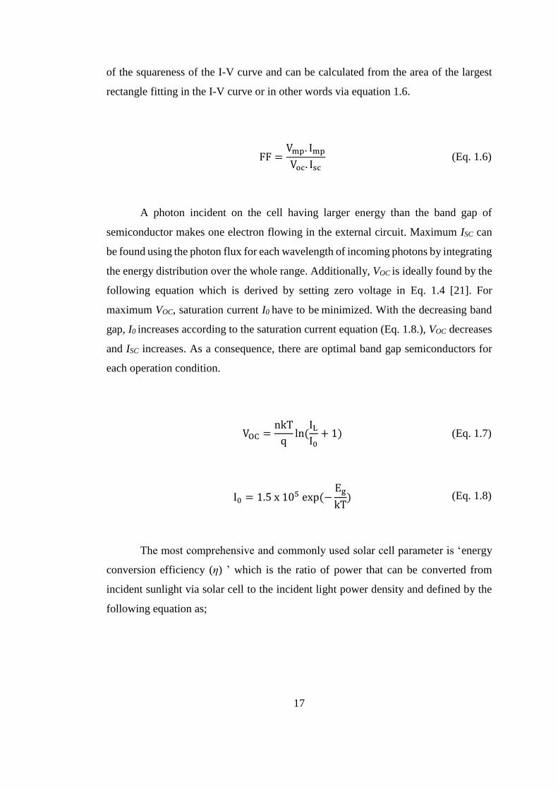
17
of the squareness of the I-V curve and can be calculated from the area of the largest
rectangle fitting in the I-V curve or in other words via equation 1.6.
FF =
Vmp. Imp
Voc. Isc (Eq. 1.6)
A photon incident on the cell having larger energy than the band gap of
semiconductor makes one electron flowing in the external circuit. Maximum ISC can
be found using the photon flux for each wavelength of incoming photons by integrating
the energy distribution over the whole range. Additionally, VOC is ideally found by the
following equation which is derived by setting zero voltage in Eq. 1.4 [21]. For
maximum VOC, saturation current I0 have to be minimized. With the decreasing band
gap, I0 increases according to the saturation current equation (Eq. 1.8.), VOC decreases
and ISC increases. As a consequence, there are optimal band gap semiconductors for
each operation condition.
VOC =
nkT
qln (
IL
I0+ 1) (Eq. 1.7)
I0 = 1.5 x 10⁵ exp (−
Eg
kT) (Eq. 1.8)
The most comprehensive and commonly used solar cell parameter is ‘energy
conversion efficiency (η) ’ which is the ratio of power that can be converted from
incident sunlight via solar cell to the incident light power density and defined by the
following equation as;

18
η =
FF. Voc.Isc
Pin=
Pmp
Pin (Eq. 1.9)
where Pin is the total power of the light incident of the cell [22].
1.3.7. Loss Mechanisms Affecting Cell Performance
There are several factors leading to reduction in the expected performance of
solar cells. Shockley–Queisser (SQ) limit refers to the maximum theoretical efficiency
limit of a solar cell made from a single p-n junction. The effects which restricts the
solar cell performance to even reach SQ limit is shown in Figure 13.
Figure 13: The major efficiency limits in the Shockley-Queisser limit at AM1.5
spectrum. Adapted from [23].
For a single p-n junction with 1.34 eV band gap, maximum conversion
efficiency is calculated to be around 33% (at AM 1.5 solar spectrum). The main losses
are due to photons with energy below band gap since they cannot be absorbed. Also

19
photons with energy above band gap results in performance losses because of the
carrier relaxation at the edges of the conduction and valence bands. Moreover, we
assume Sun as a blackbody having about 6000 K temperature while the solar cell is
assumed to be a blackbody at 300 K, so that the radiation coming from the Sun cannot
be totally captured by the solar cell at room temperature. “Other losses” term in the
Figure 13 refers to the losses due to the tradeoff between low radiative recombination
and high operating voltages [24].
However, it is important to note that this limit is not very appropriate for the
crystalline silicon solar cells because of its indirect band gap. SQ limit is calculated
based on radiative recombination mechanism, whereas in crystalline silicon cells
dominant recombination mechanism is non-radiative (Auger recombination) [23].
Taking these propertis into the account, 29.43% efficiency limit is derived for silicon
solar cells in 2013 [25].
Above all, there are additional intrinsic losses leading less efficient solar cells
than expected by the theoretical limits.
Short Circuit Current Losses
ISC losses are mainly caused by ‘optical’ nature of the cells. Reflection losses
because of highly reflective bare silicon and metal contacts on the front side of the cell
reduces ISC output of the cell. Additionally, bulk of the cell should be thick enough to
absorb enough photon to produce charge carriers. Collection probability of these
generated carriers is also important, so the recombination in the bulk and at the surface
has also significant effect on ISC losses.
Open Circuit Voltage Losses
The main reason of VOC losses is the ‘recombination’ in semiconductor. The
process of that an electron and a hole combines before being collected at the
corresponding contacts is called as “recombination”. Low diffusion length resulting
from low quality bulk material and weak passivation of the surfaces are main reasons

20
of high recombination and consequently reduce VOC. Band gap energy has also impact
on VOC and with decreasing band gap energy, VOC decreases as well.
There are 3 main recombination types named as; radiative (band to band)
recombination, Shockley-Read-Hall (through defect level) recombination and Auger
recombination. In a silicon solar cell, Auger and Shockley-Read-Hall recombination
are more dominant because the radiative recombination is less probable for indirect
band gap materials. Radiative recombination is reverse of absorption process in which
an electron from the CB directly combines with a hole and emits the resultant energy
as light Auger recombination is dominant in highly doped materials and in materials
having high impurity levels. It involves three carriers. While two carriers recombine,
the resulting energy is given to another electron in the CB which thermalizes back to
the CB edges. Shockley-Read-Hall recombination, on the other hand, is a two-step
process in which electrons are captured in an energy state in the forbidden region due
to defects before combines with a hole [22].
Fill Factor Losses
The parasitic Rsh and Rs resistances have a major impact on fill factor of solar
cells. The main contribution of Rs comes from bulk resistance of semiconductor and
the interface resistances between layers and also between the contacts and the bulk.
Rsh on the other hand, caused by the defects and impurities near the junction that leads
shorting of the junction, especially at the cell edges. High Rs values also act to reduce
ISC while low Rsh causes drop in VOC.
1.4. Monocrystalline Silicon Solar Cells
Semiconductor materials can be single- (mono-), multi-, poly-crystalline or
amorphous depending on the size of the crystals constructing the material. For the
silicon semiconductor bulk in a solar cell, either mono-crystalline or multi-crystalline
materials are used. Although multi-crystalline silicon production is cheaper and more

21
simple, grain boundaries within the material decreases its quality compared to the
mono-crystalline ones (Figure 14).
Figure 14: Schematic representation bonds in silicon semiconductor
(a) Monocrystalline (b) Multicrystalline [26].
Grain boundaries are known as regions of high recombination centers reducing
carrier lifetime and electronic properties located at the boundaries between two crystal
grains. Hence, with the well-defined band structure and regular arrangement of silicon
atoms, single-crystalline solar cells have better material parameters although they are
more expensive. Besides, with the drop in silicon price over the past years, single-
crystal silicon has become much more attractive for solar cell production with a current
market share of about 35% in 2015 [27]. Common mono-crystalline growth techniques
include Czochralski (Cz) and Float Zone (FZ). Cz wafers are the most commonly used
ones besides despite the high amount of impurity. FZ wafers are used to overcome this
problem with its more complicated growth technique and higher cost.
1.4.1. Standard Silicon Solar Cell
A standard silicon solar cell consists of high concentration of dopants at the
both sides of the wafer, phosphorus diffused front side and aluminum-doped back side

22
as shown in Figure 15a schematically. Traditional solar cells generally based on p-type
crystalline silicon (c-Si) wafer. This kind of n+pp+ structure is generally named by
“aluminum-back surface field (Al-BSF)” solar cells Figure 15a. In the textured p type
silicon wafer, electrons and holes are extracted from the front and the back sides
respectively. Silicon nitride on the front side acts both as surface passivation and anti-
reflection coating (ARC) layer. Aluminum on the back side play a role as p+ dopant
source besides back contact.
Figure 15: (a) Schematic of the standard Al-BSF solar cell [28], (b) Analysis of
recombination losses (PC1D model) [29].
In a study published recently, this structure was modelled with representative
industrial solar cell parameters using PC1D modelling program and predicted a
maximum efficiency of 21.1% with the recombination loss analysis [29]. Standard
fabricated silicon solar cells reached efficiencies up to 20.29% [30] for
monocrystalline and 17.8% [31] for multicrystalline silicon substrates. It is obvious
that the recombination at rear metal contact is dominant loss mechanism in addition to

23
the recombination in the absorber region, phosphorus diffused region and front surface
(Figure 15b).
Fabrication of standard solar cell starts with the texturing of 180 µm thick p-
type waferschemical cleanings, high temperature phosphorus diffusion. Since this
diffusion is done on both sides, back side diffused region needs to be etched off or
overcompensated by p doping. n+ type layer on the front generally has sheet resistance
of between 50-100 Ω/sq. An ARC layer is subsequently deposited to minimize the
reflection from the cell and to passivate the surface. For metallization, front side
fingers and busbars are made by Silver printing with appropriate masks. The rear side
of the cells is fully covered by full Aluminum by the same printer. A subsequent firing
step allows to form front contacts through silicon nitride layer. It also overcompensate
P doped n-type region previously created during phosphorus diffusion on rear side by
driving in Al into the bulk of Si, leading to creation of a p+ layer which provides an
electric field called Back Surface Field (BSF) pushing the minority carriers away from
the interface region.
1.4.2. High Efficiency Solar Cell Concepts
Although the standard solar cells are cost effective and easy to process, their
efficiency potential is obviously limited. In the last two decades, new device concepts
with high efficiency potential have been introduced and realized at R&D laboratories.
Moreover, more recently, it has been shown that the cost of these highly efficient can
be reduced to affordable levels. Among others, interdigitated-back-contact (IBC),
silicon heterojunction (HTJ), passivating contact solar cells or even the combination
of them have proven to be promising technology alternatives from both efficiency and
cost point of view.

24
1.4.2.1. Interdigitated Back Contact Solar Cells
In the IBC design, collection of both type of carriers is done at the rear side of
the cell which allows fully optically active front side. This design is advantageous both
in terms of optics and electronics because there is no trade-off between series
resistance and grid shading. Since no metal is placed on the front side, high ISC values
are achievable as a result of high incident photon flux on the front side. Additionally,
this cell structure is easier to interconnect and may be placed closer to each other in
the module because it is not necessary to leave space between cells.
Although there are many possible fabrication sequences, the main goal is to
create interdigitated p+ and n+ patterns, alternatively named as emitter and back surface
field (BSF) respectively on the back side as shown in Figure 16. Boron diffusion is
generally implemented to the back surface to transport holes selectively while
phosphorus is diffused to gather electrons. The underlying reason of having larger
emitter regions than BSF is that the electron mobility is higher than hole mobility.
Hence, for better carrier collection, larger fraction of p+ region is preferred. The
openings between these two regions must be large enough for less contact resistance
losses and sufficiently small to have less recombination because of direct contact of
the metal to the silicon. To avoid any possible shunt between back side electrodes,
electrodes are generated slightly narrower.
Figure 16 shows the back contacted cell structure produced in a collaborative
work of Australian National University, Trina Solar and PV Lighthouse in 2014,
resulted in 24.4% cell efficiency from 2 × 2 cm2 cell area [32].

25
Figure 16: Cross-section representation of the IBC cells fabricated in [32].
It is also common to create an additional lightly diffused n+ layer on the front
side to make electrons flow laterally through this layer before being collected from the
back side. The design of IBC solar cells can vary according to the additional layers
such as passivation and anti-reflection.
With the further developments mainly on reduction of edge losses and series
resistance, SunPower broke the efficiency record with n type monocrystalline IBC
technology (X-Series), achieving 25.2% on a full area (153.5 cm2), under one-sun
operation, using industrial processes [33].
1.4.2.2. Silicon Heterojunction Solar Cells
Different from homojunction solar cells, two different semiconductor materials
namely amorphous hydrogenated silicon and crystal silicon (a-Si:H and c-Si) rather
than diffused emitter and c-Si create the p-n junction in heterojunction solar cells.
Hydrogenated amorphous silicon is used for many years due to its excellent
passivation quality on the c-Si surfaces.

26
Figure 17: Structure of Panasonic’s heterojunction solar cell [34].
Although Sanyo was the pioneer of the c-Si heterojunction solar cells, they
changed their brand name of solar modules Sanyo to Panasonic in 2012. Afterwards,
Panasonic has broken the heterojunction conversion efficiency record with 24.7% in
2013 on 101.8 cm2 solar cell area from the heterojunction with intrinsic thin layer
(HIT) solar cell structure shown in Figure 17. HIT solar cell includes an intrinsic (i-
type) and a p-type a-Si layers deposited on n type c-Si crystalline silicon wafer to form
a p-n junction and also i-type and n-type a-Si layers on the opposite side to get a BSF
structure. Additional Transparent Conductive Oxide (TCO) layers and electrodes are
also produced on both sides of the cell [34].
Thanks to the intrinsic thin a-Si:H layer that gives us excellent surface
passivation, HIT solar cells attains high Voc values. Additional benefits of this structure
includes low processing temperatures which is lower than 200 ºC meaning less
contamination and less damage on the bulk. It is believed that there are still some
possibilities to further raise the conversion efficiency with higher quality of the a-Si
film and more optimized front electrode size to reduce shadow loss and hence to gain
much more from Jsc.
Further improvements and higher conversion efficiency on HIT cell structure
came from Kaneka Corporation in 2015 by optimization of process conditions with
25.1% conversion efficiency on 151.9 cm2 cell area. This is the latest world record in
a both-side-contacted heterojunction silicon solar cells [35]. The main improvement

27
they have made was the reduction in interface carrier recombination which causes
improvement in FF and hence in overall efficiency.
1.4.2.3. Passivating Contact Solar Cells
Since the recombination at surfaces and under metals is one of the major
obstacle against very high conversion efficiencies, surface passivation has primary
importance in solar cell design. However, the challenging part is decreasing surface
recombination and conducting electrical current simultaneously. Recombination at
contacts needs to be minimized in order to get low saturation current density (J0,contact).
Furthermore, the requirement of carrier selectivity should be fulfilled allowing one
type of charge carrier while blocking the other type which is necessary to get a high
external open circuit voltage (VOC). To perform these requirements, the structure is
created by generally depositing a thin interface oxide layer and a conductive thin film
on the silicon wafer. In order to obtain high fill factor (FF) from such structures having
several layers and interfaces, having low contact resistivity is also necessary for
majority carrier transport.
Although in the literature “carrier selective” term is also used on behalf of
“passivating”, there are different conditions to be fulfilled for an ideal contact in a
carrier selective structure. A great passivation layer may not be carrier-selective
because it blocks both electrons and holes. Similarly, a perfect carrier-selective contact
may not serve good passivation [36].
Doped silicon layer and very thin insulating layer is needed under the metal
region in this structure (Figure 18). The silicon layer can be either deposited directly
as polycrystalline silicon or as hydrogenated amorphous silicon. Phosphorus or boron
dopants can be defined in situ [37] or they can be subsequently introduced by ion
implantation [38], by thermal diffusion from a gaseous source [39] or from a doped
oxide [40]. In order to crystallize the amorphous silicon layer and to activate dopants
simultaneously, subsequent temperate process is performed. In most of the cases, this

28
temperature process is followed by a hydrogenation process from a plasma or
annealing in a gaseous environment which includes nitrogen and hydrogen, to further
improve passivation properties.
In 2015, The Fraunhofer Institute for Solar Energy Systems (ISE) achieved
new world record from such a cell with a full area passivating back contact with 25.1%
conversion efficiency. After one and half years later, they increased their former record
by 0.6 % absolute, with the developments in the same cell structure (Figure 18), and
their updated record conversion efficiency to 25.7% (2 × 2 cm2 area). This so-called
TOPCon (Tunnel Oxide Passivated Contact) technology has shown the highest
efficiency achieved to date for both sides-contacted monocrystalline silicon solar cells
[41].
Figure 18: Structure of TOPCon solar cell [37].
This record cell structure includes very thin wet chemically grown tunnel oxide
and Plasma Enhanced Chemical Vapor Deposition (PECVD) based in-situ
phosphorus-doped a-Si:H layer which has been semi-crystallined after high

29
temperature treatment. The cell properties will be discussed in detail later in
experimental part of this thesis.
There are plenty of studies on passivating contact cell structures in the last
years. Yet another both side contacted passivating contact structure has been studied
by Energy Research Centre of the Netherlands (ECN) with their bifacial solar cell,
namely PERPoly structure, shown in Figure 19. Bifaciality allows light to enter from
both sides different from entire metal covered back surface TOPCon structure
discussed.
Figure 19: Structure of PERPoly solar cell [42].
Another point of difference from the record efficient TOPCon cell structure is
that they employed industial screen printed passivating contact cells in their 21.3%
efficient PERPoly structure from large area (239 cm2) [42].

30
1.4.2.3. Novel Solar Cell Concepts
With the intention of pushing the efficiencies towards the theoretical limit of
29.43% (for a 110-μm-thick Si wafer) [25], combinations of different high efficiency
solar cell concepts have been recently on rise.
Heterojunction Back Contact (HJBC);
Since heterojunction solar cells achieve high VOC and FF values with their high
minority lifetime advantage, and IBC solar cells promises good optical properties
which enhances Jsc values. Higher efficiencies are achieved by combining these two
concepts. In 2014, the highest efficiency in a silicon solar cell of 25.6% (144 cm2) was
reached by a HJ back contact cell [43].
Recently, a Japan company, KANEKA Corporation has reported the world’s
highest conversion efficiency from mono c-Si solar cell with industrially compatible
large-area cell (179.74 cm2). Associating interdigitated back contact design with an
amorphous silicon/crystalline silicon heterojunction structure (Figure 20), they have
achieved photoconversion efficiency of 26.6% which is an absolute improvement of
1% relative to the 25.6% [44]. This cell was the first to exceed 26% conversion
efficiency among the equivalent c-Si technology counterparts.

31
Figure 20: The cell structure of Kaneka Corporation [45].
Additionally, they have shown practical attainable efficiency limit of HJBC
cell as 27.1%, using their device design and fabrication processes with their best
quality HJ passivation. KANEKA’s real device result confirmed the potential of HJBC
device with the approximately 10% reduction of the remaining loss to theoretical limit
[45].
IBC with Passivating Contact;
Another structure combining two different cell concepts is introduction of
passivating contacts to IBC structure. While IBC structure provides the optical gain,
passivating contacts enable to get high open circuit voltages via low recombination
rates at the surfaces. Recently, Institute for Solar Energy Research Hamelin (ISFH)
has achieved a solar cell efficiency of 25% (3.97 cm2) from such a structure shown in
Figure 21. This high efficiency was achieved with their “poly-Si on oxide” namely
POLO structure which avoids recombination under metal contacts for both polarities
on the back side.
The contact includes thin silicon oxide and doped polycrystalline silicon layer
as in the case of TOPCon cell structure. However, here the difference is no contact is
placed on the front side of the cell. For the electrical current conduction from thin

32
silicon, they utilized localized current flow through pinholes in the oxide while in
TOPCon structure, it has been done by tunneling effect which will be discussed in the
next chapter, this thesis.
Figure 21: IBC with POLO junction cell structure of ISFH [46].

33
CHAPTER 2
THEORY
2.1. Background Information
2.1.1. Contacts and Contact Resistivity
In this chapter, contact types including Schottky and ohmic contacts, their
formation, contact resistance and resistivity parameters will be explained. Contacts
between semiconductor and metal and the effect of the existence of an insulating layer
between them will be discussed.
2.1.1.1 Metal-Semiconductor Contacts
The formation of metal-semiconductor (MS) contact is important for most of
the electronic and photovoltaic devices. MS contacts do not necessarily have low
resistances as contacted two metals because of the mismatch between the Fermi levels
of metal and the semiconductor. This difference may also result in high resistance
rectifying contact. In such a contact, the flow of carriers is easier in one direction than
it is in the other direction. In Figure 22, the energy band diagrams of a metal and n-
type semiconductor (a) before contact formation and (b) after contact formation in
equilibrium case is drawn for the case of a Schottky contact formation.

34
(a) (b)
Figure 22: Band diagrams of a metal and a semiconductor before Schottky contact
formation (a), after Schottky contact formation in equilibrium (b).
When semiconductor and the metal are contacted, a barrier is formed at their
interface which is responsible for current flow control. EM,F corresponds to metal Fermi
level. The delocalized electronic states lead conduction around this level. WFM is the
metal work function that is the energy difference between vacuum and EM,F. Similarly,
WFSC is semiconductor work function and χ refers to the electron affinity [47].
If WFM is greater than WFSC (for n-type semiconductor), a Schottky contact is
formed resulting in a barrier at the contact interface between metal and semiconductor.
The energy difference between the metal work function and the electron affinity of
semiconductor determines the Schottky barrier height denoted as ΦB,n and ΦB,p for n
and p-type semiconductor respectively according to the Schottky-Mott rule [48]. This
barrier height is important as it acts as a potential barrier against charge carriers and
affects the electrical features of the device [49]. A Schottky diode is preferred in low
voltage and high current applications because there is lower voltage drop across the
diode terminals when current flows compared to a normal pn junction diode. Majority
carriers are responsible for carrier transport in Schottky contacts while in p-n junctions
minority carriers are the responsible ones.
In a MS contact, main majority carrier transport is carried out by thermionic
emission (TE) over the barrier to the metal. In a TE, the depletion region is wide to

35
make electrons to jump over the potential barrier as in the Figure 23a. So the current
flow in a Schottky contact governed by TE is given as below [50].
𝐽𝑆 = 𝐴∗𝑇2𝑒(
−2Φ𝐵𝑘𝑇
)(𝑒𝑞𝑉/𝑘𝑇 − 1) (Eq. 2.1)
where A* is Richardson’s constant, q is the elementary charge, k is the
Boltzmann constant and T is the temperature. Hence, the resulting current has a non-
linear relation with the voltage (Figure 23a) which depends on the barrier height and
the temperature.
Figure 23: Conduction mechanisms for metal/n-semiconductor contacts. Thermionic
emission (a), thermionic-field emission (b), field emission (c). Adapted from [51].
Ohmic contact is also one type of metal semiconductor contacts in which the
Schottky barrier height is low, or negative (Figure 23c). In Figure 23, conduction
mechanisms for metal/n-semiconductor contacts is shown with increasing doping
concentration from a to c. For lowly doped substrates where ND < 1017 cm-3, TE

36
dominates as in the Figure 23a case while b shows Thermionic-Field Emission (TFE)
with intermediate doping 1017 < ND <1019 cm-3 and finally c shows high doping with
ND > 1017 cm-3 in which the barrier is sufficiently thin making Field Emission (FE) to
be the dominant mechanism [52].
Contrary to Schottky contacts, ohmic contacts allow carrier flow in both
directions with very low contact resistances. Hence, ohmic contacts show linear
current voltage dependence. Another way to achieve an ohmic contact is to decrease
the depletion width so that carriers can tunnel by thermionic field emission (if the
barrier height is also lower) or field emission (FE) through a thin barrier at interface
(Figure 23b and Figure 23c) [51]. Current flow for semiconductor-metal tunneling
contact case is given below.
𝐽𝑠𝑚 =
𝐴∗𝑇
𝑘∫ 𝐹𝑆 𝑃(𝐸)(1 − 𝐹𝑚)𝑑𝐸 (Eq. 2.2)
where Fs and Fm refers to the semiconductor and metal’s Fermi-Dirac
distributions while P(E) refers to the tunneling probability. If Fs, Fm and P(E) is
replaced, more explicit equation may be found as follows.
𝐽𝑠𝑚 𝛼 exp (−2𝑥𝑑√
2𝑚∗(𝑞Φ𝐵 − 𝑞𝑉)
ℎ2 ) (Eq. 2.3)
Here, xd is the depletion region width, while m* is the effective mass of the
tunneling carrier and h is the Plank's constant.

37
2.1.1.2 Metal-Insulator-Semiconductor Contacts
The interface of MS structure is modified by placing a thin insulator between
metal and the semiconductor. The insulator acts as a tunnel barrier which allows one
type of the charge carrier to tunnel with some probability. This insulator may either be
a dielectric or sometimes a semiconductor like amorphous silicon as in the case of HTJ
solar cells. Barrier width and barrier height have the major importance in this case
because the tunneling probability mostly depends on these parameters.
Resultant Metal-Insulator-Semiconductor (MIS) contact has lower contact
resistivity values than MS contacts [53]. However, still there is a trade-off between
reduced resistance after lowering barrier height and increased resistance from the
tunneling through the insulator. If the interlayer is amorphous silicon rather than a
dielectric, it can be thicker than a dielectric film because the carrier transport
mechanism will be different [54].
2.1.1.3 Contact Resistance and Specific Contact Resistivity
In order to investigate the contact quality, suitable methods & evaluations and
well-defined terms are needed to be measured and identified. In 1972, Berger has filled
this deficiency by clearly describing the terms related to contacts of electronic devices
[55]. Contact resistance (Rc) is defined to be the additional resistance as an obstacle to
reach ideal contact. It represents the resistance between semiconductor and metal
contacts, which can be high depending on the electronic properties of the interface. A
contact may behave like a nonideal contact due to the differences in work functions of
metal and semiconductor, surface states or multiple foreign layers introduced
inbetween.
In order to characterize metal-semiconductor interface independent of the
contact geometry or semiconductor bulk characteristics, the term called as specific

38
contact resistivity or contact resistivity (ρc). When the current distribution at the
contact is uniform, Eq. 2.4. can be used to determine contact resistivity.
𝜌𝑐 = 𝑅𝑐 • 𝐴𝑐 (Eq. 2.4)
where Ac is the contact area. More widely used form to calculate ρc becomes as
Eq. 2.5. which shows the ratio of total voltage drop Vc across the layers to Jc current
density at the contact. More accurately, for a MS and MIS contact, the current transport
is characterized by its specific contact resistivity which has the unit of [Ω·cm2] and
defined under dark conditions as;
𝜌𝑐 ≈ (
∂ V
∂ J)
𝑉=0
(Eq. 2.5)
where V is the voltage applied and J is the current density.
The quality of the contact is characterized by contact resistance which is
sometimes assumed to be negligible compared to the series resistance. Characterizing
ohmic contacts includes many difficulties in terms of measurement and evaluation.
Main difficulty is to separate the metal-semiconductor interface resistance from the
semiconductor bulk resistance. There are some basic and also advanced methods to
separate contribution of different interfaces which will be discussed later in this
chapter.

39
2.1.2. Tunneling
Tunneling is a quantum mechanical concept in which carriers pass through a
barrier that they are not able to do it in classical conditions. Because electron has
wavelike property and the waves do not end suddenly at a barrier or a wall, contrary
to the classical case, it can either tunnel through barrier, or decay out after certain
penetration into the barrier. This can occur even if the energy of the electron is much
smaller than the barrier height. In the classical case, only the carriers with enough
energy can escape the barrier as in the case of TE. Using time dependent Schrödinger’s
equations, probability of electron tunneling can be determined [49].
Adding an insulator between metal and semiconductor interface results in
change in work functions and reduces Schottky barrier height. As the tunneling
probability depends on the barrier width, the thickness of insulator between metal and
semiconductor should be well controlled. If the barrier is thin, insulator’s additional
resistance will be low enough to save the advantages of this Schottky barrier reduction.
So the overall contact resistance will be lower as expected. As the tunneling barrier
becomes thicker, additional resistance increases exponentially and dominates the total
contact resistance. According to a simulation study done by Roy, A.M. in 2012, there
is a lowest limit for the thickness of this insulator to get barrier reduction together with
the highest limit to obtain low contact resistivity [56].
2.1.3. Recombination and Passivation
Electrons excited to the CB eventually decay back to the lower energy empty
VB states removing a hole. This process is known as recombination. The average time
passes between the generation of the carrier and their recombination is called carrier
lifetime, which is a crucial parameter for devices. The ratio of excess concentration of
carriers, Δ𝑝 or Δn, to the net recombination rate, U (cm-3s-1), gives the carrier lifetime.

40
The recombination process is separated into two main types as bulk
recombination and surface recombination. Since recently, the quality of wafers has
been enhanced, the main recombination centers became the high carrier concentration
regions and also the cell surfaces. To avoid these losses, surface states have to be
“passivated.” In order to have higher conversion efficiencies from a solar device, both
of these recombination types must be minimized since they cause loss of carriers
within the device.
Within the bulk, there are three types of recombination which are Shockley-
Read-Hall (via defect states), Radiative (band to band) and Auger. The Radiative and
Auger Recombination are intrinsic recombinations while Shockley-Read-Hall (SRH)
Recombination is extrinsic with its high defect dependence. Furthermore, Auger and
SRH recombination are the dominant ones for silicon solar cells because of its indirect
band gap. These processes are shown in Figure 24.
Figure 24: Bulk recombination processes
Radiative recombination is reverse the of the absorption process and usually
occurs in direct band gap semiconductors since an additional phonon emission is
required to conserve momentum in indirect band gap materials. In Auger
recombination case, electron recombining with a hole gives resulting excess energy to
a second electron rather than emitting as a photon. Then, this second excited electron

41
emits photon while relaxes back to its original position. Because, more than two
carriers are included in this process, it is more likely to happen in highly doped
materials. SRH recombination, on the other hand, is a two-step recombination
mechanism including a defect level in the forbidden region in which electron gets
trapped before relaxing to the valence band [22].
All types of recombination mechanisms must be taken into account to
determine the lifetime of material. The bulk lifetime then can be found via the
following equation.
1
Ƭ𝑏𝑢𝑙𝑘=
1
Ƭ𝑟𝑎𝑑𝑖𝑎𝑡𝑖𝑣𝑒+
1
Ƭ𝑆𝑅𝐻+
1
Ƭ𝐴𝑢𝑔𝑒𝑟 (Eq. 2.6)
Surfaces also introduce additional recombination centers since the crystal
lattice is incomplete at the surface resulting in dangling bonds. They promote the
electron-hole recombination at the surfaces by acting as intermediary level for carrier
transfer between CB and VB. The surface recombination rate is measured by the
minority carrier transfer rate headed to surface which is called surface recombination
velocity. Surface passivation is needed to reduce surface recombination and hence raise
the efficiency of the device.
The lifetime of the material may be enriched by suppressing the surface
recombination velocity via passivation. The passivation at the surfaces can be done
either through reducing number of dangling bonds (chemical passivation) or reducing
the concentration of one carrier type at the surfaces. Reducing number of dangling
bonds is performed through growing or depositing a layer on top of the surface to
chemically bind the dangling bonds to atoms. This layer can be a dielectric or
amorphous silicon. This chemical passivation may also be performed by additional
hydrogen atoms introduced to the surface via hydrogen annealing. Furthermore,
reducing one type of carrier number at the surfaces is performed by introducing a field
to the surface as a result of bend alignment at the physical junction, by an external bias

42
or by a passivating dielectric layer (field effect passivation) [47]. Increasing surface
dopant density decreases the surface recombination velocity especially for the surfaces
passivated with a dielectric layers.
Bulk and surface recombination contributes together to the effective lifetime
which is expressed by;
1
Ƭ𝑒𝑓𝑓=
1
Ƭ𝑟𝑎𝑑𝑖𝑎𝑡𝑖𝑣𝑒+
1
Ƭ𝑆𝑅𝐻+
1
Ƭ𝐴𝑢𝑔𝑒𝑟+
1
Ƭ𝑆𝑢𝑟𝑓𝑎𝑐𝑒 (Eq. 2.7)
2.1.4. Passivating Contacts – Trade-off between passivation and contact
resistivity
Traditional homojunction solar cells commonly have surfaces in direct contact
with metal and remaining area is passivating with a dielectric. As the regions under
the metal are critical obstacles against reaching high efficiencies with their high
recombinative potential. However, reducing the metallized region is not a solution
because of the limited carrier travel length, so it is necessary to provide passivation
under these metallized areas. However, as the most of the passivating materials are
insulators, decreasing the surface recombination and conducting the current at the
same time is challenging. One way to achieve simultaneously both of these properties
is to use hydrogenated amorphous silicon semiconductor with a very thin dielectric
layer in between. This approach is also very similar to the MIS structures discussed in
the previous sections where a microcrystalline silicon layer with a dielectric such as
silicon dioxide is used. High efficiency values obtained for this structure were
announced in 1980’s [58]. Furthermore, most of the current back contacted cells with
record efficiencies also utilize passivating contact to achieve very high VOC values.
Recent passivating contact examples are the TOPCon technology [41] and
POLO technology [46] that yields very high efficiency values using an ultra-thin

43
silicon oxide layer and a heavily doped deposited silicon layer. The idea of using an
ultra-thin silicon oxide layer between metal and semiconductor is based on the MIS
structure and contemporarily applied to a p-n junction device. In the TOPCon device,
this ultra-thin silicon oxide layer is required to allow one type of charge carrier while
blocking the other type, based on the quantum mechanical tunneling approach as
mentioned in the previous sections. Because of this selective tunneling issue, the oxide
thickness must be well-controlled and usually less than 25 Å is required for current
transport. The application of tunneling oxide and deposited n+ silicon layer at full back
side of the n type solar cell structure (Figure 18) has led to 25.7% conversion efficiency
for 4 cm2 cell area [41]. However, for p type devices with p+ silicon layer, these high
efficiency values could not be achieved so far. It may be related to different pathways
for carriers while tunneling, large valence band offsets and problems originating from
boron defects. The band diagram of TOPCon structure is illustrated in the Figure 25a.
On the other hand, in the POLO approach (Figure 25b), the current flow occurs through
the pinholes generated intentionally within the oxide layer.
Figure 25: Band diagram of TOPCon structure (a), carrier flow in POLO approach
(b).
As discussed also in the first chapter in this thesis, low saturation current
density (J0) is required as an indication of low recombination at the metallized
(J0,contact) and non-metallized (J0,pass) surfaces separately. J0,pass values are expected to
be typically few orders of magnitude lower than J0,contact ones. Hence, there exists a

44
trade-off between passivating the surfaces and obtaining good contact. The former is
characterized by J0 (A·cm-2) while the latter is characterized by ρc (Ω·cm2). To show
this trade-off between these parameters, Bullock et.al. performed a simulation on
idealized solar cell structure (Figure 26). It is illustrated that to obtain high efficiencies,
keeping both J0 and ρc low is a necessity [59].
Figure 26: Simulated resultant efficiency as a function of J0, ρc and the contact
fraction (dotted lines). Adapted from [59].
It is apparent to achieve high power conversion efficiencies, obtaining J0 below
10 fA/cm2 and ρc below 1 mΩ·cm2 is necessary. It also strongly depends on the contact
fraction. For the full area contacts, in other saying, unity contact fraction, having
higher contact resistivity is acceptable as long as the passivation is fairly high.
Reduction in contact fraction constricts the carrier flow towards metal-silicon interface
and results in reduced conduction. Hence, reducing the contact fraction requires
gradually lower contact resistivity values in order to stay in high efficiency region
according to simulation done by Bullock et al [59].

45
2.2 Characterization Techniques
In order to evaluate the properties of passivating layers used in this thesis work,
different methods were used such as quasi-steady-state photoconductivity lifetime
measurements, electrochemical capacitance-voltage, spectroscopic ellipsometry,
secondary ion mass spectroscopy, raman spectroscopy and contact resistance
measurement techniques. Yet, the focus of this thesis will be on contact resistivity
analysis of these layers.
2.2.1 Quasi-steady-state Photoconductivity (QSSPC)
Minority carrier effective lifetime can be obtained either by transient or the
Quasi-steady-state photoconductance method (QSSPC). For this purpose, Sinton
Instruments WCT-120 lifetime tester is used and the measurement setup is illustrated
and sketched in Figure 27.
Figure 27: Sinton Instruments WCT-120 lifetime tester. Illustration of the tool (a),
Sketch of the setup (b).

46
Measurement starts with a short flash to generate excess charge carriers and
enhance the conductance, after the flash is over, conductance decay again. Relatively
longer flash is used in the QSSPC case than in transient measurements in order to keep
generation rate constant over a short time. The setup records the conductance over time
via the coil coupled to a radio frequency (RF) generator and calculates excess charge
carrier density from the photoconductance change applying Eq. 2.8.
∆σ = qW(µ𝑛 + µ𝑝)∆n (Eq. 2.8)
where ∆𝜎 refers to the variation in photoconductance, W is the thickness of the
sample, µ𝑛 and µ𝑝 are the mobilities of electron and hole carriers respectively. After
then, effective lifetime of the sample, Ƭ𝑒𝑓𝑓 is calculated by;
Ƭ𝑒𝑓𝑓 =
∆n
𝐺 − ∂∆n
∂t
(Eq. 2.9)
where G is photogeneration rate of the excess carriers. G can be neglected in
the transient measurement while in the QSSPC technique, G becomes important.
Implied open circuit voltage value can also be extracted from the measured data via
the following equation. Implied circuit voltage indicates the maximum achievable VOC
in current state of the sample.
iVoc =
𝑘𝑇
𝑞ln (
𝑛𝑝
𝑛𝑖2) (Eq. 2.10)

47
where n and p are the total electron and hole concentrations respectively, ni is
the intrinsic carrier density, k is the Boltzmann constant and T is the temperature of the
sample.
The measurement output also gives the inverse lifetime graph on the main
purpose of extracting total saturation current density J0 measured under high injection
conditions. From the slope of the linear fit to this graph, J0 value is extracted. However
if the sample does not include diffused conductive surfaces or the low injection levels
are used instead of high injection levels , then it is less possible to get linear fit and
extracted J0 value does not have a physical meaning [60].
2.2.2 Electrochemical capacitance-voltage (ECV)
Wafer profiler CVP21 tool is used to quantify the doping profiles via active
carrier concentration measurement within the semiconductors by Electrochemical
Capacitance Voltage (ECV) profiling method. The measurement setup is shown in the
Figure 28. Even though it is a destructive method, it provides limitless measurement
depth through the sample and easiness in sample preparation.
Figure 28: ECV Measurement Setup. Adapted from [61].

48
This method includes etching the surface of the cell and measuring the
concentration of the carriers repeatedly in order to identify the electrically-active
dopant concentration for each depth. Electrolyte within the sealing ring etches the
surface and the ring opening identifies the contact area. A Schottky diode is utilized
between sample and an electrolyte and charge of the ions in the solution decides
carriers to be attracted or repelled. As a result, when the depletion region is created,
ionized donors generate a capacitive effect. By applying an external voltage, the width
of depletion layer can be changed and hence the capacitance changes accordingly.
Equations for depletion width and capacitance is given by
𝑊𝑑 = (
2(Ø − 𝑉)ε0ε𝑟
𝑞𝑁)1/2 (Eq. 2.11)
𝐶 = 𝐴(
𝑞𝑁ε0ε𝑟
2(Ø − 𝑉)) (Eq. 2.12)
where Wd stands for the depletion region, C corresponds to capacitance, Ø is
the built in potential, V is the applied bias voltage, A is the contact area and, 휀0 and 휀𝑟
are the permittivities of free space and the semiconductor respectively.
From the capacitance, determining carrier concentration, N, is done through
the Equation 2.13 [61].
1
𝐶2=
2(Ø − 𝑉)
𝑄𝑁ε0ε𝑟𝐴2 (Eq. 2.13)

49
2.2.3 Spectroscopic Ellipsometry (SE)
Spectroscopic Ellipsometry (SE) is a non-destructive and contactless thin film
characterization technique. Generated light in an initial polarization state interacts with
the sample surface and reflected from the surface with a different polarization state.
This change in the polarization states allows the analysis of the layer in terms of some
properties such as layer thickness, refractive index, absorption coefficient or even
crystallinity (Figure 29).
Figure 29: Configuration of Spectroscopic Ellipsometry.
Main measured data in SE are called as amplitude ratio, Ψ and phase shift, Δ.
These parameters are related to the intensity of decoupled s and p components of the
reflected light via Equation 2.14. Measured amplitude ratio and phase shift can be
transferred to many other parameters as refractive index or thickness of the layer by
doing some computer analysis. This computer analysis part includes modelling and
adjusting fit parameters to estimate the fit parameters [62].
𝜌 =
𝑅𝑝
𝑅𝑆= 𝑡𝑎𝑛Ψ𝑒𝑖Δ (Eq. 2.14)

50
where 𝜌 is the reflectance ratio. The film thickness and optical band gap of
silicon layers after deposition were determined by SE, in this thesis study.
2.2.4 Raman Spectroscopy
Raman spectroscopy is a technique providing information about molecular
vibrations and crystal structures of the concerned material. Monochromatic light is
generated by laser in visible, near infrared (IR) or near ultraviolet (UV) range and used
to irradiate the sample. The molecule interacted with the incoming photon change its
rotational and vibrational states. Raman bands results from change in polarizability of
molecule after interaction. Hence, scattered laser photons is shifted which can be
detected in Raman system via CCD camera. This shift in energy gives information
about vibrational modes of the molecule.
In this thesis, Raman spectroscopy was used in order to examine the
crystallinity of the a-Si deposited layers after the annealing steps. Since the as-
deposited a-Si Raman peak and the peaks of other crystallized layers differs in peak
frequency, crystallinity of the deposited layers can be checked after annealing steps.
2.2.5 Contact Resistivity Measurements
In order to enhance the cell performances, accurate determination of contact
resistivity is needed especially when the cell structure has passivating layers with
multiple interfaces and is contacted with a fraction less than unity. There are number
of ways to assess the performance of ohmic contacts to semiconductors and quantify
the contact resistivity ρc.
The methods used so far in the literature are usually for conventional simple cell
structures withouth many layers and the ρc values reported are not accurate but indeed
relative values. Hence, it is very important to determine contact resistivity of these

51
high efficiency cell structures accurately. Furthermore, it is desired to differentiate the
several interface contributions. Discussing and comparing different approaches on
contact resistivity determination of different cell structures including passivating
layers is the main purpose of this thesis. Additionally, a numerical model using solar
cell simulation tool Quokka 3 to evaluate accurate contact resistivity and separate out
the contributions from different interfaces is developed and applied on some of the
structures. This numerical simulations also offers information about individual layers
aside from the interfaces.
2.2.5.1 1D Transmission Line Method Evaluation
To define the specific contact resistivity within the metal semiconductor
interface, Transmission Line Method (TLM) was first suggested for planar ohmic
contacts by Shockley in 1964 [63]. In this technique, contacts were separated by
variable distances from each other and the current is constrained to flow from one
metal contact into semiconductor sheet and up into second metal contact pad. From
the voltage drop associated with this current flow, the total resistance encountered is
calculated. This voltage drop measurement can be done by a multimeter and from the
ratio of voltage drop to current applied, total resistance is obtained. This resistance
between any two contacts can be plotted as a function of distance between these
contacts as illustrated in Figure 30 below.

52
Figure 30: Plot of the total resistance as a function of distance between metal
structures together with a linear fit.
The resistance of a single contact is identified as the sum of the metal resistance
and contact resistance. However, since the resistance of metal in the contact is so small
that contact resistance dominates, metal resistance can be disregarded. RC in Figure 30
refers to the contact resistance at the metal/semiconductor interface. Incrementing
separation between the metal pads are named as d1, d2... (Figure 31) and having more
altered gap distances yields more precise results with the need of least 3 different gap
distances. The resistance value at the zero gap distance interception gives twice of the
contact resistance which can be found from the plot by extrapolating to d=0. Slope of
the linear fit gives the sheet resistance divided by the contact length Z. However, as
the contact resistance is influenced by the size of the contact, as an alternative, contact
resistivity is used as a point of evaluation and comparison.

53
Figure 31: Typical arrangement for a TLM pattern. Cross section (a), top view (b).
The lateral current flow through the semiconductor is usually uniform, yet the
fraction of vertical flow between semiconductor and metal contacts is not the same
throughout the metal. Hence, the physical length and width of the contact does not
state the real active contact area. Major current transfer from the semiconductor to the
metal contact pads or vice versa occur at the edges of the contacts and it declines
moving away from the edge, as illustrated in Figure 32. This behavior is known as
“current crowding effect” which was developed by Hower et al. [64] and decides the
effective length of the contact. Then, transfer length, LT, ought to be taken into
consideration and can be measured from the interception at R=0 by extrapolating to
the horizontal axis. This interception point refers to -2LT .
Figure 32: Sketch of current flow path showing the transfer length.

54
Apart from the extraction of transfer length from the interception point of the
linear fit, more accurate determination can be done via numerical solution of Eq. 2.16
for LT after sheet resistance calculation from the slope. For small metal distances
linearity of the R(d) curve fails. Therefore, larger pad distances are desired for sheet
resistance extraction from the slope but smaller pad distances are also crucial for
accurate interception points. Then, all parameters are known to find contact resistivity
which is calculated via Eq. 2.17 assuming to have electrically long contact W>LT [65].
𝑅𝑠ℎ𝑒𝑒𝑡 = 𝑚 ∗ 𝑍 (Eq. 2.15)
𝑅𝐶 =
𝑅𝑠ℎ𝑒𝑒𝑡
𝑍∗ 𝐿𝑇 ∗ coth (
𝑊
𝐿𝑇)
(Eq. 2.16)
𝜌𝑐 = 𝑅𝑠ℎ𝑒𝑒𝑡 ∗ 𝐿𝑇2
(Eq. 2.17)
Even though some parameters are extracted using the simple analytical theory
of TLM, it should not be forgotten that there are so many assumptions which are not
compatible with up-to-date designs. Assumptions cover;
The effect of bulk is disregarded.
Thin conductive layers (diffusion, poly Si, etc.) are not involved.
Metal layer resistance is ignored.
Current trails from the edges of the metal are ignored.
Only one effective interface is taken into the account.
Hence, 1D-TLM measurement overestimates the contact resistivity value
because of the ignored additional resistances (from bulk, metal and different
interfaces) which can not be clearly separated from contact resistivity. There are
numerous TLM evaluations including the correction for the current flowing around the
contact edges or using circular structures in order to discard this effect [66]. However,
there is no non-assumptive evaluation which gives definite contact resistivity values.

55
2.2.5.2 2D Transmission Line Method Evaluation
Since the 2 dimensional (2D) current transport through the bulk of the silicon
was ignored in standard 1D TLM evaluation, Eidelloth and Brendel suggested an
analytical expression for extraction of the contact resistivity from TLM measurements
taking the current flowing through the bulk into consideration for samples with any
thickness [67]. Even if this method stands for correcting the bulk effect, it does not
comprise a lateral edge effect correction. The metal layer is also expected to be
infinitively conductive as in 1D TLM case. They additionally provide numerical
simulations in order to verify the experimental results.
This method accounts for the thickness and the resistance of the bulk
semiconductor since they both affect the length and the curvature of the current
streamlines (See Figure 33). Likewise 1D TLM evaluation, R(d) plot should be formed
as well as the interception point with the resistance axis, b, and the slope, m at large
gap distances. Dimensionless geometry factors (G2D-TLM, G1D-TLM, GCM) were defined
in order to extract contact resistivity value. After the ratio of interception point to slope,
b/m is extracted from the plot, using the related equations, 2D bulk corrected contact
resistivity value can be obtained independent of the contact length Z in line with the
paper of Eidelloth and Brendel [67].
𝛾 =
𝑊2𝜌𝑏
𝜌𝑐ℎ (Eq. 2.18)
𝛿 =
ℎ
𝑊
(Eq. 2.19)
where 𝛾 is used in order to calculate G1D-TLM from the usual solution of 1D-
TLM theory. 𝛿 becomes a part of these calculations when GCM is calculated. GCM is

56
described as G2D-TLM factor when contact resistivity goes to zero, in other words limρc→0
(G2D-TLM) by conformal mapping approach.
𝐺1𝐷−𝑇𝐿𝑀 = √𝛾 𝑐𝑜𝑡ℎ√𝛾 (Eq. 2.20)
𝐺𝐶𝑀 = 1 + 𝛾 + 𝛾
𝛿
𝜋(𝑙𝑛4 − ln (𝑒
𝛿𝜋 − 1))
(Eq. 2.21)
Combining these two formulas produces an analytical expression for 𝜌𝑐which
is valid for arbitrary thickness and bulk resistance (Eq.2.22). It is obvious that 𝐺1𝐷−𝑇𝐿𝑀
refers to 𝐺2𝐷−𝑇𝐿𝑀for infinitively small sample thicknesses.
𝑏
𝑚
𝜌𝑏𝑊
2𝜌𝑐ℎ= 1 + √((𝐺1𝐷−𝑇𝐿𝑀 − 1)2 + (𝐺𝐶𝑀 − 1)2 (Eq. 2.22)
‘(G1D-TLM-1)’ term in the equation refers to the resistance by a supplementary
transport length below the contact parallel to the surface. ‘(GCM-1)’ term represents the
resistance due to vertical transport perpendicular to the surface below the contact.
Contact resistance contribution is added as 1, unity. However, both in this and their
subsequent work, it is stated that this model is not reliable for the values below 1
mΩ•cm2 [46-67]. Furthermore, assumptions like single interface layer, current flow at
the edges, infinitively high metal conductivity and not including thin conductive layers
are still valid. Yet, this evaluation is more accurate than the 1D evaluation to some
extent.
2.2.5.3 3D Simulations via Quokka 3
In addition to the TLM measurements and 1D and 2D evaluations, another
method is developed in order to evaluate contact resistivity using as less assumptions
as possible. This section is based on the study done and to be published with the title
of “On the determination of the contact resistivity for passivating contacts using 3D

57
simulations” [68]. A 3D numerical model is used by the 3rd version of Quokka solar
cell simulation tool in which a solver for ohmic carrier transport was additionally
developed [69]. This simulation tool can be used constituting up to two conductive
layers at each side of the bulk including sheet resistances and contact resistivities at
the interfaces. Therefore, it may be used to represent TLM structures on more
complicated devices having more than one interfaces and interlayers. Since devices
including passivating layers are used in this thesis work, evaluation via Quokka 3
simulations were well suited for the main aim.
Physical properties like bulk resistance, thickness, size and position of the
TLM patterns, gap distances between them should be well-defined to the simulation.
Knowing the sheet resistance of each layer makes additional contribution. After
defining the identical properties as experimental case, the contact resistivity can be
extracted where the match between experimental R(d) data and simulation R(d) data
occurs (See Figure 33). This contact resistivity represents the sum of contact
resistivities at each interface between individual layers. The contact resistivities can
be further distinguished using the same simulation tool if the silicon layer’s
conductivities are adequately high and an etching process is applied in between the
metal pads to eliminate the conductive layers in-between.
Figure 33: TLM geometry as defined in Quokka3 (a), R(d) match between
experimental data and the numerical simulations (b).

58
The only assumption in this case is the metal conductivity which is taken to be
infinitively high because of some limitations about simulation tool. However, metal
layer conductivity was also observed to have no sufficient effect on the result, with an
additional simulation set [68]. Profitably, any specific geometry can be defined, 2
conductive layers at each side can be included with 2D bulk. Since an alike
characterization device to the experimental structure is formed in the simulation tool,
this technique seems to be the most precise evaluation way although it has a time-
consuming structure which may be enhanced with future developments.
2.3 Concepts Investigated in This Thesis
There are many high efficiency and novel solar cell concepts apart from the
conventional Al-BSF solar cell as presented in the first chapter of this thesis. On the
purpose of examining contacts of some of these solar cells, characterization samples
regarding to these cell concepts were fabricated and analyzed.
Electron beam (e-beam) evaporated in-situ doped (n) passivating contact,
PECVD deposited in-situ doped (n) TOPCon passivating contact and LPCVD
deposited and ex-situ doped (n) Poly-silicon passivating contact structures are the
major investigated cell designs (Figure 34). e-beam evaporated structure is fabricated
in e-beam evaporation system from Vaksis company in The Center for Solar Energy
Research and Applications (GÜNAM) laboratories, Middle East Technical University,
Turkey. Other two structures were fabricated in the tools from Roth and Rau company,
located in Fraunhofer Institute for Solar Energy (ISE) laboratories, Germany.
All of the characterization samples are produced by both side polished wafers.
It is not necessary for TLM, ECV, Raman and SE measurements to have symmetrical
samples as shown in the Figure 34, but for the QSSPC lifetime measurements,
symmetrical samples are required. In order to carry out all the characterizations from
the same sample, they were fabricated symmetrically.

59
The e-beam evaporated in-situ (n) doped amorphous layers were fabricated
symmetrically on top of a very thin tunnel silicon dioxide layer (Figure 34a). One of
the well-known methods to obtain poly-crystalline silicon layers is the solid phase
crystallization (SPC) method by thermal annealing using in-situ doped amorphous
layers as starting material. [70]. Thermal annealing of amorphous layers affects the
grain size of deposited layer which can be analyzed via Raman measurements. After
the characterization steps of QSSPC, Raman, metal TLM structures were defined on
the front side for further characterization as contact analysis. The fundamental
fabrication details will be described in Chapter 3. In the present study, the influence of
thermal annealing temperature was investigated in terms of crystallinity, passivation
and contact resistivity.
The other fabricated structure is PECVD based n-TOPCon passivating layer
(Figure 34b). This structure includes a very thin tunnel oxide on both sides. n type
amorphous crystalline layer is symmetrically deposited by PECVD. Subsequently, a
high temperature annealing step is applied to partially crystallize amorphous layer in
addition to simultaneously obtain diffusion layer underneath and activate the dopants.
This time, characterization steps include QSSPC and contact resistivity measurements.
The influence of the different procedures to get thin tunnel oxide, annealing
temperature after deposition of n-TOPCon layer and the metal type on contact
resistivity was investigated.
Final structure has very similar working principle as the TOPCon, where poly-
crystalline silicon passivating layers were used. Contrary to the TOPCon structure, the
deposition of intrinsic amorphous layer is done via Low Pressure Chemical Vapor
Deposition (LPCVD) for poly-crsytalline Si layers (Figure 34c). Subsequently, ion
implantation method is used to implant this layer with Phosphorous to obtain n type
doped layer, namely ex-situ doped. Next thermal treatment is done to crystallize the n
type layer, to diffuse and activate the dopants as mentioned in the previous sections
related to other structures investigated in this study.

60
Figure 34: Contact resistivity characterization structures investigated. e-beam
evaporated in-situ (n) doped silicon layer (a), (n) TOPCon in-situ doped passivating
layer (b), (n) Poly-silicon ex-situ doped passivating layer (c).

61
CHAPTER 3
SAMPLE PREPARATION
The concepts investigated in this thesis were separated into 3 sections as
mentioned in the previous chapter. e-beam evaporated (n) layers were fabricated and
characterized in GÜNAM laboratories. Other structures including (n) TOPCon and (n)
poly-Silicon layers were entirely produced and characterized in Fraunhofer ISE
laboratories.
3.1. Fabrication Procedure for e-beam Evaporated Layers
n type shiny-etched float-zone (FZ) silicon wafers with 200 µm thickness and
1 Ω·cm base resistivity were used in fabrication and characterization in GÜNAM
laboratories. n type amorphous silicon layers structures were fabricated symmetrically
in order to be able to perform QSSPC measurements. The fabrication sequence can be
seen in Figure 35 for both contact resistivity and passivation characterization samples.
Following the standard Radio Corporation of America (RCA) cleaning step, a
short Hydrofluoric (HF) acid dip is performed. RCA cleaning is the very first step of
silicon solar cell or characterization samples production [71]. This cleaning step is a
must in order to remove metallic and organic residuals at the sample surface followed
by dip samples into HF solution, rinse in the Deionized (DI) water and make it dry.
RCA cleaning done in GÜNAM laboratory includes subsequent RCA-1 and RCA-2
cleaning procedures. Ingredients of these solutions were prepared and mixed with
magnetic stirrer while it was heated up to 70ºC ± 5 ºC. 10 minutes treatment for each
cleaning solution was performed at this temperature.

62
Since these cleaning treatments oxidize the surfaces as mentioned in previous sections,
HF dip and drying under nitrogen environment is performed to obtain clean surface.
The surface after HF dip is expected to be hydrophobic which means non-wetting
surface.
Figure 35: Simplified process sequence for the fabrication of the e-beam evaporated
layers characterization.
Tunnel oxide formation was done symmetrically on cleaned surfaces of the
wafer via wet chemical nitric acid oxidation method.
Nitric Acid (HNO3) Oxide (NAOS)
NAOS refers to the Nitric Acid Oxidation of Silicon method. Wafers were
dipped in boiling 68 wt% (i.e. azeotropic mixture with water) nitric acid solution at
100 °C to form thin (~1.4 nm) tunnel oxide layer on both sides. Azeotropic mixture

63
refers to a solution of two liquids (in this case nitric acid and water) in which the
density does not change upon vaporization during boiling, in other words constant
boiling solutions. Since the concentration of nitric acid remains constant, the process
is accepted as reproducible. Atomic oxygen is the oxidizing agent reacting with the
Si/SiO2 interface after the breakdown of the reaction [72];
2HNO3 2NO + H2O + 3O
Subsequent to tunnel oxide formation, n type amorphous layers were deposited
by e-beam evaporation or in another saying e-beam physical vapor deposition
(EBPVD) system at 9.0x10⁻⁸ Torr base pressure and approximately 5x10⁻⁸ Torr process
pressure. The deposition was done when the substrate temperature was 400 °C
temperature. Evaporation rate was kept at 1Å/s. Passive dopant concentration is
expected around 5.25x10²⁰ atoms/cm3 according to the previous ToF-SIMS
measurements.
Figure 36: Schematic representation of e-beam evaporation system. Adapted from
[73].

64
The schematics of the EBPVD vacuum system is shown in the Figure 36. The
material to be evaporated on substrate, which is silicon in this case, is melted by beam
of electrons emitted from charged filament under high vacuum (10-6-10-7 Torr). The
material to be evaporated is separated from the filament by a water-cooled crucible in
order to protect the filament from possible contaminations. Electron beam bends
towards the material with the help of magnetic field. Atoms of concerned material
leaves target to coat the surface of substrate.
EBPVD is known with better control and higher deposition rates than the other
vapor deposition systems. Impurity level is lower than thermal evaporation but higher
than PECVD techniques. Although the uniformity of the layers is not as good as
PECVD systems, EBPVD may be preferable in terms of lower cost and high
directionality of the system.
e-beam evaporation customized system by Vaksis company used in the
GÜNAM laboratories is sketched in Figure 37. This system includes additional
effusion cells for p type and n type doping via boron element and gallium phosphide
compound respectively. In this thesis, only n type was required and utilized. P atoms
were separated from GaP compound by sublimation using a particular pyrolytic Boron
Nitride crucible which causes efficient trap for Ga atoms.
Figure 37: e-beam evaporator system in GÜNAM laboratories. Adapted from [74].

65
Following the n type layer deposition, tube furnace annealing was done to
obtain poly-silicon layers instead of amorphous ones. 2 different temperatures and time
(800 and 900 °C, each for 2 and 4 hours) were employed to see the effect of
temperature and time of annealing on layers in terms of different aspects. Crystallinity
analysis via Raman and iVOC measurements by QSSPC were done before and after this
annealing step. SIMS was additionally performed in order to see the dopant profiles
after annealing steps.
In order to define TLM pattern on top of these layers, TLM hard masks were
prepared as shown in Figure 38 via laser cut. Hard masks were placed on top of the
samples before putting them into the thermal evaporation system. Ag metal is
thermally evaporated to form TLM contacts. The vacuum level in the thermal
evaporation system was below 1.0x10⁻⁵ Torr.
Figure 38: Defined TLM pattern prepared by laser cut.
Metal pad widths of 600 µm and lengths of 2000 µm were used for TLM
contacts. The range of gap distance between each metal is from 260 µm to 480 µm.
Lower gap distances could not be obtained because of the limitations related to hard
mask fabrication. A short anneal for contact formation was realized at 200 °C for 20

66
minutes. The setup for measuring I-V via four point probe measurements and Keithley
Digital Multimeter were used to extract resistance associated to each different metal
separations. Following to determination of resistance as a function of metal pad gap d
for each sample, 1 and 2 dimensional TLM evaluations were implemented for contact
resistivity analysis.
3.2. Fabrication Procedure for (n) TOPCon Layers
Differently from the previous section, the fabrication of (n) TOPCon layers
were carried out in Fraunhofer ISE Clean Room. For characterization of these layers,
symmetrical samples were prepared whose cross-sections were shown in the Figure
34b. The fabrication sequence can be seen in Figure 39.
Figure 39: Simplified process sequence for the fabrication of the n-TOPCon
passivating layers characterization.

67
n type shiny-etched float-zone (FZ) silicon wafers with 200 µm thickness and
1 Ω·cm base resistivity were used. Subsequent to RCA cleanings, a short Hydrofluoric
(HF) acid dip is performed. Since RCA process leaves a thin oxide at the surface which
should be removed afterwards, HF dip was performed to remove this thin oxide from
the surface as mentioned before.
Next, a tunneling dielectric layer had to be defined on both sides of the clean
sample. This layer may be one of various materials such as silicon dioxide, silicon
nitride or aluminum oxide. However, silicon dioxide is mostly used tunneling
dielectric thanks to its low fixed and interface trapped charge density potential in
comparison with the other materials [75]. An extremely thin silicon dioxide layer is
formed simultaneously on front and the rear side of the sample. Additionally, non-
oxidized sample was also included in the experimental set of (n) TOPCon layers.
Different ways were performed to grow thin oxide (1.3-1.5 nm) layers.
Nitric Acid (HNO3) Oxide (NAOS)
NAOS refers to the Nitric Acid Oxidation of Silicon method. Wafers were
dipped in boiling 68 wt% (i.e. azeotropic mixture with water) nitric acid solution at
120 °C to form thin (~1.4 nm) tunnel oxide layer on both sides as mentioned in
previous section.
Ozonated DI Water Oxide
Ozone is a suitable wet chemical oxidizing material which can be used either
for removal of contaminations on the wafer surface or surface passivation. Since ozone
has a powerful oxidizing material, ozone based wet chemical oxidation is performed
using ozonized DI water. Reactions that may occur during ozonated DI water oxidation
is shown in Table 1.

68
Table 1: Possible reactions occur during formation of O2 at silicon surface [76].
Initial Step Intermediate Step Decompositon to O2
Si-H + O3 Si- + HO3 Si-OH + O2
Si-H + O3 Si-O + HO2 Si-OH + O2
Si-H + O3 Si- + OH + O2 Si-OH + O2
O3 reaching to the surface decomposes into O2 and atomic O. Atomic O has
much shorter lifetime whereas O2 is less reactive and causes oxidation of Si-H bond.
HO3, HO2 or OH radicals are formed at intermediate steps resulting in formation of
silicon oxidizing agent O2 at the end [76].
Oxide from UV/O3 Sources (Excimer and Hg vapor lamp)
There are also ozone based oxidation techniques. This time the oxidation is
performed in dry atmosphere rather than wet-chemical oxidation. UV/O3 photo-
oxidation is performed using two different sources as Hg vapor lamp and an excimer
source in ozone ambient (Figure 40).
Figure 40: Reaction mechanisms and schematics of Hg vapor lamp (a), excimer
system (b). Adapted from [77].

69
In the Hg lamp system, photons with different special wavelengths are
generated in order to be absorbed by O2 to produce atomic O and generate O3 as a
result of reaction between O and O2 at the same time (Figure 40). Simultaneously, in
the chamber, O3 separates in O2 and some other radicals. Produced O and O3 reach and
oxidize the wafer surface. Similarly, in excimer source systems, monochromatic UV
light is generated resulting in similarly oxidizing the surface. The distance of the lamp
to the surface to be oxidized can be varied as well as the time of exposure. The time
and distance variations are expected to change the quality and the thickness of the
oxide created.
After the thin tunnel oxide formation, 15 nm thin Phosphorus doped a-Si layer
(n-TOPCon) was deposited by AK-400 PECVD tool (Figure 41) on both sides of the
sample. Using the mixture of some reactive gases as SiH4 (silane), CH4 (methane) with
dopant gas PH3, and forming the plasma, deposition of doped layer was carried out.
AK-400 PECVD tool includes a process chamber and a load lock parts
separated as shown in Figure 40. Microwave and radio frequency power generators
are used to excite the reactive gases and to fire the plasma. Subsequent to the electron
excitation with the help of plasma environment, electrons start to make collisions with
molecules and cause chemical reactions.

70
Figure 41: Schematic Representation of AK-400 PECVD tool at Fraunhofer ISE
[78].
As a consequence of the difference between bulk plasma potential and surface
potential, acceleration of ions towards the electrodes occurs, in other words ions are
bombarded onto the substrate surface. As a result, some of the produced gas phase
radicals hold on the substrate surface and initiate a chemical reaction there.
On the purpose of activating the dopants in deposited amorphous layer and
moreover to partially crystallize this layer, subsequent furnace annealing was
performed under N2 environment. Samples were exposed to 800 – 900 °C
temperatures. For lower temperatures, longer exposure times were utilized. For non-
oxided samples, only 900 °C annealing was performed where an additional 800 °C
annealing is added for other samples. The iVOC and lifetime results were obtained by
QSSPC measurements after the furnace annealing step.
While annealing in the tube furnace, oxide may grow unintentionally, so this
oxide was removed by short HF dip. In order to get further passivation, Remote Plasma
Hydrogen Passivation (RPHP) technique was used. The RPHP tool used is shown in
Figure 42. There is a microwave generator to obtain plasma from the gas mixture at
about 400°C. A large number of atomic hydrogen H+ is generated and since they are
fast diffusers and active species for passivation of defects or impurities, they diffuse

71
and further reduce interface recombination. Pressure should not be high to prevent H
collisions with each other. The wafers were exposed to hydrogen plasma for 30
minutes. Then, the passivation quality was checked again using the QSSPC technique.
Figure 42: Schematic Representation of RPHP tool at Fraunhofer ISE [79].
Then, the samples were prepared for contact resistivity analysis by utilizing a
photolithographically defined TLM pattern. TLM contacts are formed by thermal
evaporation of Ti/Pd/Ag or Ti/Pd/Al stacks and the following lift-off technique. The
TLM geometry used is shown in Figure 43.
Metal pad widths of 600 µm and lengths of 2000 µm were used. The range of
gap distance between each metal is from 20 µm to 240 µm. Resistance as a function
of metal pad gap d was measured for each sample for further contact resistivity
evaluations.
1 and 2 dimensional TLM evaluations were implemented after the R(d) plot
formation. For one specific sample (HNO3 oxided, 900 °C annealed sample), 3
dimensional evaluation was additionally included using Quokka 3 simulation. For a
detailed analysis on the contact resistivity of this specific sample, plasma etching was
applied to remove the conductive layers between metals and R(d) plot was also

72
obtained after this removal. Microwave plasma source SLAN (SLit ANtenna) from JE
Plasma Consult, was used for that purpose using SF6 as the reactant gas.
Figure 43: Transmission Line Method pattern defined by photolithography
3.3. Fabrication Procedure for (n) poly-Si Layers
Similar to TOPCon passivating contact structure, symmetrical poly-silicon
passivating layers were prepared on planar n-type FZ, 1 Ω·cm, 200 µm thick wafers.
The fabrication was done in clean room of Fraunhofer ISE laboratories (Figure 44).

73
Figure 44: Simplified process sequence for the fabrication of the n-poly passivating
layers characterization.
After similar RCA cleaning and the following oxide removal by HF, tunnel
oxide formation was done by two wet chemical methods. Only nitric acid and ozonized
DI water oxidation was carried out in poly-silicon contacts case. Then, undoped
amorphous silicon was deposited via LPCVD reactor at 485 °C. The LPCVD
deposition was separately done at the Institute for Microsystems Engineering
(IMTEK), Freiburg. In LPCVD process, pressure is lower relative to the other
Chemical Vapor Deposition (CVD) processes. Due to this low pressure, diffusion of
reactant gases decline resulting more uniform and homogeneous layers [80]. Inside of
a typical LPCVD reactor is shown in the Figure 45. Quartz tube is heated with the
spiral heaters to preferred temperature at a low pressure. Reactive gases are sent to the
tube to react with the substrate and form desired layer on the substrate surfaces. 40 nm

74
was the target thickness of a-Si for this study, nevertheless the real thicknesses were
measured after the deposition using spectroscopic ellipsometry.
Figure 45: Schematic Representation of LPCVD Process [81].
Afterwards, ion implantation was used to dope this undoped a-Si layer with
Phosphorus at 2 keV to form n type poly-silicon layer. 4 different doses were used
between 7.5e14 to 15e14 cm-2. Ion implantation is one of the existing doping techniques
which occurs via bombarding the sample surface with accelerated ions with the help
of an electric field. Representation of a usual ion implanter is illustrated in Figure 46.
Dopants are ionized within the ion source and accelerated by accelerator. Lenses are
used to focus the ion beam. Desired ions are separated using mass separator with the
help of their atomic mass differences. In order to remove the created additional
damages during ion implantation process, annealing step is a must. Under the nitrogen
ambience, samples were received 30 minutes annealing in tube furnace at temperatures
of 850 °C and 900 °C.

75
Figure 46: Illustration of an Ion Implanter [81].
Next, wafers were exposed to RPHP at 400 °C for 30 min for further
passivation. The passivation quality was analyzed by QSSPC technique before and
after RPHP step. Additional ECV measurements were taken to clearly see the profiles
of doping and the diffusion from poly layer to silicon for each ionization dose.
Then, the samples were prepared for contact resistivity analysis, similar to
TOPCon layers case. Photolithography was used for defining the same TLM pattern
as in Figure 43. Ti/Pd/Al stack is deposited by thermal evaporation and following lift-
off. TLM geometry and the dimensions are identical to the one in TOPCon passivating
layer case. R(d) plot was drawn for each case subsequent to the I-V measurements via
a probe station and Keithley 195/196 System Digital Multimeter (DMM). Various
TLM evaluations including 1D and 2D were done following to measurements.
Additional 3D evaluation using Quokka 3 simulation was also done for one particular
sample (HNO3 oxided, 850 °C annealed sample). For a detailed analysis on the contact
resistivity of this specific sample, plasma etching was also applied to remove the
conductive layers between metals and R(d) plot was also obtained after this removal.

76

77
CHAPTER 4
RESULTS AND DISCUSSIONS
The theory underlying passivation layers and characterization of these layers
considering open circuit voltage and contact resistivity have already been described in
detail in Chapter 2. The focus of this thesis is on the contact resistivity analysis of these
layers. Implied VOC is also discussed in order to analyze contact resistivity and contact
passivation behavior at the same time. In this chapter, the effect of different parameters
on passivation and contact resistivity are presented. Contact resistivity measurements
were done via Transmission Line Method measurements as explained in previous
sections. The evaluations were done via 3 different evaluation techniques one of them
which is common old method in the literature [63]. The other method was proposed
recently by Eidelloth and Brendel [67]. Third evaluation method was developed in this
thesis work and could only be applied to one specific sample from two out of three
passivation layer types [68].
4.1. (n) e-beam Evaporated Passivation Layer
Following the main cleaning steps, thin nitric acid oxides were formed wet
chemically and symmetrically on the sample. The characterization of this thin tunnel
oxide was not additionally done within the scope of this thesis since the wet chemical
nitric acid oxide formation has already been optimized at GÜNAM laboratories.

78
Following the oxide formations, deposition of n type doped a-Si layers were
carried out via e-beam physical vapor deposition (EBPVD) system. Target thickness
of this layer was about 40 nm and since the process has been already optimized, no
further check for thickness was done. Before and after the n type doped a-Si layer
deposition, Raman and QSSPC measurements were carried out. Then, solid phase
crystallizations (SPC) were done in the tube furnace and additional Raman and QSSPC
measurements were done in order to extract implied VOC values before and after SPC
step. For SPC, four combinations were performed including two different temperatures
and 2 different annealing times. Figure 47 illustrates implied Voc values just after the
(n) a-Si layer deposition, after 2 hours and 4 hours annealing at 800 °C and 900 °C
temperatures.
Figure 47: Implied Voc values before and after Solid Phase Crystallization (SPC).
As can be clearly seen from the Figure 47, passivation is inversely proportional
to the annealing temperature and annealing time as expected since high annealing
temperatures increases the recombination velocity at the silicon-dioxide/c-Si interface.
Annealing time has a positive impact on passivation quality since the crystallization

79
increases when the time of annealing increases. Whereas the iVoc was around 525 mV
after the a-Si layer deposition, it reached almost 665 mV after 4 hours annealing at 800
°C. It can be further developed and optimized in order to reach best passivation with
this layer.
Sheet resistance of the upmost layer was checked with 4-point-probe sheet
resistance measurement. As the larger grain sizes were expected when increasing the
annealing temperature and time, sheet resistance of these layers were expected to
decrease when exposed to higher temperature treatments and longer times. Figure 48
shows the sheet resistance measurements from 4 different points on the sample
including front side deposited and back side deposited layers. The layer shows high
homogeneity within a layer and between front and back side of the same sample. The
sheet resistance of the layer before any SPC annealing step measured around 300 Ω/.
For 900 °C annealing, longer annealing causes approximately 5 Ω/ drop in sheet
resistance. For 800 °C annealing, increasing annealing time raises sheet resistance
unexpectedly.
Figure 48: Sheet resistance of crystallized layers after different treatments

80
Raman spectroscopy measurements were also carried out just after the a-Si
layer deposition and after SPC treatments. Figure 49a illustrates the Raman spectra
measured from the sample revealing the presence of highly-crystalline (blue and
green) and non-crystalline (black) as deposited layer and the partially crystallized
states in between [82]. Highly crystalline silicon has very sharp peaks for instance the
one centered at ~ 520 cm-1 as can be seen in Figure 49a. Figure 49b exemplarily shows
focused projection of the same Raman spectroscopy after background subtraction. a-
Si peak which is at ~ 480 cm-1 disappears after 900 °C, 2 hours annealing.
Figure 49: Raman spectroscopy of layer as deposited and after crystallization via
variable conditions (a), exemplarily illustration of disappearance of a-Si peak after
SPC (b).
Subsequently, TLM pattern was formed by hard mask and metal was defined
by thermal evaporation using approximately 300 nm Ag. Following the metal
formation, short anneal for contact formation was performed. For the TLM
measurements, total resistances were measured for several different contact spacing
and corresponding R(d) vs. resistance plots were created (Figure 50). As mentioned in
Chapter 2, some of the parameters were extracted using simple analytical old TLM
evaluation based on many incorrect assumptions.

81
Figure 50: Comparison of R(d) graphs of samples with varying annealing conditions
for SPC.
Although there is no good linearity in the resistance vs. distance plots as shown
in Figure 50, it is possible compare the contact quality of different conditions and even
to extract contact resistivity values. From the R(d) plot, it is obvious that the lowest
contact resistivity is obtained from the sample with 900 °C, 4 hours annealing from
the interception point at d=0. Even though the other samples have quite close contact
resistivity values to each other, 900 °C, 2 hours annealing shows the second lowest
contact resistivity which is followed by the sample annealed at 800 °C, 4 hours
annealing. The contact resistivity values were evaluated using oldest 1D-TLM method
mentioned in Chapter 2. 2D bulk corrected method published by Eidelloth and Brendel
were also performed and contact resistivities were extracted using the same R(d) data.
The results are shown in Figure 51.

82
Figure 51: Contact resistivity values evaluated by 1D-TLM method (a), evaluated by
2D-TLM method (b).
Both 1D-TLM and 2D-TLM evaluation results shows that contact resistivity
decreases with increasing annealing temperature and annealing time (Figure 51).
However, extracted contact resistivity values are ultra-high for a good contact. The
non-linearity in the R(d) graph were also a sign of poor contacting. The reason behind
that maybe the quality of the metal layers deposited or the non-uniformity in the oxide
layer in-between silicon layers. Increasing the annealing time or temperature may be
a solution, however the passivation would reduce since there is a trade-off between
contact resistivity and passivation.
4.2. (n) TOPCon Passivation Layer
Subsequent to main cleaning steps, thin tunnel oxides were symmetrically
formed on the sample. The characterization of these tunnel oxides were not
additionally done within the scope of this thesis since these oxide formations have
already been studied in detail and optimized at Fraunhofer ISE. Following the oxide
formations, deposition of n type doped a-Si layers were carried out via PECVD. Target

83
thickness of this layer was about 15 nm and since the process has been already
optimized, no further check for thickness was done.
Then, tube furnace anneal was performed and QSSPC measurements were
done in order to extract implied VOC values before and after hydrogenation step. In this
part of the thesis, only after RPHP iVOC values will be given and compared to each
other. Subsequently, TLM pattern was formed via photolithography and metal was
defined by thermal evaporation. Ti/Pd/Ag and Ti/Pd/Al metals were used.
Figure 52: iVoc after RPHP of various oxide layers including Hg lamp oxide time
and distance variations.
The data in Figure 52 originates from cooperation with the colleague
F.Feldmann from Fraunhofer ISE. It shows the detailed passivation optimization of
Hg lamp oxidation various time and exposure distances. For instance, Hg 0.5/1
represents the exposure from the distance of 0.5 cm between lamp and the sample for
1 minute. UV/O3 stands for the excimer source. Surface passivation improves with
longer exposure time and smaller distances for Hg lamp. Before continuing with the

84
contact resistivity measurements, one of these Hg lamp oxide samples was chosen.
Since the best implied VOC was obtained from the Hg 0.5 cm/3 min sample annealed
at 800 °C, contact resistivity analysis work continued with only this sample for
comparison with the other oxides. Best passivation was obtained from DI-O3 and
excimer UV/O3 oxides amongst all oxide layers. However, only DI-O3 oxide was
observed to be stable after annealing at 900 °C (Figure 53). For other oxides, increasing
annealing temperature decreases the passivation quality. For no oxide sample,
passivation is extremely poor with very low iVOC values even after RPHP.
Figure 53: iVoc after RPHP of various oxide layers including best Hg lamp oxide.
Lines are for visual guide.
Figure 54 is an example for the R(d) graphs of samples with nitric acid oxide.
The same analysis was carried out for each sample. For the sample with nitric acid
oxide annealed at 900 °C, applied metal type does not change the contact resistivity
with the value of around 2.1 mΩ·cm2 after 1D-TLM evaluation. However, for the

85
sample annealed at 800 °C, Ti/Pd/Al metal leads to lower contact resistivity (4
mΩ·cm2) than the Ti/Pd/Ag metal (6.75 mΩ·cm2).
Figure 54: Comparison of R(d) graphs of samples with HNO3 oxide
It is obvious that annealing temperature has a significant effect on passivation
and contact resistivity. From Figure 55, it is observed that the contact resistivity is
inversely proportional to the annealing temperature for 800-900 °C temperature range.
The lower annealing temperature leads the better the passivation properties after
hydrogenation step (Figure 53). This behavior can be attributed to the strong band
bending at the poly-Si/c-Si interface which hinders carriers to diffuse into the bulk.
Moreover, high annealing temperatures end up with the increasing of recombination
velocity at the silicon-dioxide/c-Si interface and within diffused region through c-Si
bulk. So, it is clearly seen that there is a trade-off between contact properties (ρcontact)
and passivation quality (iVOC) in terms of annealing temperature.

86
Figure 55: Contact resistivities of the samples with Ti/Pd/Al metal evaluated using
1D-TLM (a), Ti/Pd/Al metal evaluated using 2D-TLM (b). Lines are for visual
guide.
Figure 55a shows the contact resistivity value which is evaluated using old 1D-
TLM method as discussed in the previous chapters for Ti/Pd/Al metal case. Figure 55b
stays for the same samples as Figure 55a, but this time 2D-TLM evaluation was
applied where 2D bulk correction was carried out. 2D-TLM evaluation gives much
lower contact resistivity values than old 1D-TLM evaluation method since the old one
already overestimates the contact resistivity. Still, 2D-TLM evaluation is not reliable
enough as it was already stated in the publication of M. Rienäcker et al. (2016). This
model is not applicable for small contact resistivity values such as ρc ≪ 1 mΩ•cm2
[46]. For some samples, 2D evaluation gives no result and could not be included
especially when ρcontact was very large (>30 mΩ•cm2) or very small (<1 mΩ•cm2).

87
Figure 56: Contact resistivities of the samples with Ti/Pd/Ag metal evaluated using
1D-TLM (a), Ti/Pd/Ag metal evaluated using 2D-TLM (b). Lines are for visual
guide.
UV/O3 excimer lamp oxide shows worse contact properties than the other
samples. Non-oxided sample shows low contact resistivity than the other samples as
expected since no insulator layer is presented between the conductive layers. However,
it is observable that 900 °C annealed HNO3 sample shows as good contact resistivity
as non-oxided sample with a contact resistivity around 0.50 mΩ•cm2 after 2D-TLM
evaluation. For samples annealed at 800 °C, DI-O3 oxide shows higher contact
resistivity than HNO3 oxide whereas optimized Hg lamp with 0.5 cm/3 min exposure
parameters shows the best contact resistivity. For samples annealed at 900 °C, results
are much more close to each other. The contact resistivity of all samples are lower than
that of samples annealed at 800 °C except UV/O3 Hg lamp sample where ρcontact is
observed to be stable with increasing annealing temperature.
Additional 3D numerical simulation was carried out for one specific sample
with good passivation properties using Quokka version 3. Since the simulation
includes as few assumptions as possible and it represents very similar TLM structure
to experimental case, results seem to be more reliable than the other two evaluation

88
methods. However, simulation could not be implemented for all the samples since the
simulation method is brand new and more time-consuming. After extracting the
contact resistivity of one specific sample, others can be relatively estimated since
trends are already known from 1D-TLM and 2D-TLM evaluations.
For the 3D Quokka Simulation, plasma etching was additionally applied to
remove conductive layers between metals on the front side as illustrated in Figure 57.
The chosen sample was the one with nitric acid tunnel oxide, annealed at 900 °C for
10 minutes with Ti/Pd/Al used for metallization . This specific sample has already
shown larger than 1 ms lifetime after hydrogenation and QSSPC extracted overall
sheet resistance was 39.8 Ω/ before etching step. R(d) plot before and after this
etching step was obtained and realistic simulations were done trying to get a match
between experimental R(d) graphs before plasma etching and R(d) graph that
simulation gives. The same was applied for after plasma etching using the same sheet
resistance and contact resistivity values also used before plasma etching. In this way,
contact resistivity of each interface could be separated and the sheet resistance of
TOPCon layer and diffused layers could be obtained.
Figure 57: The illustration of plasma etching applied to the front side of one specific
(n) TOPCon sample.

89
Differentiation of resistivities between metal/TOPCon interface (ρc1) and
TOPCon/bulk interface (ρc2) could be done via this new method with the help of
plasma etching coupled with numerical simulations. ρc1 and ρc2 were found to be 0.1
and 0.25 mΩ•cm2 respectively for the specific sample. TOPCon layer’s sheet
resistance was found to be 100 kΩ/ where the underlying diffusion layer is much
more conductive with the sheet resistance of 200 Ω/. Calculating the total resistance
of the whole structure considering all the layers and the bulk as parallel resistances,
sheet resistances are found to be around 33.31 Ω/ and 39.98 Ω/ before etching and
after etching the front side respectively (Figure 58). After the etching of front side
layers, total sheet resistance is expected to approach bulk resistance value which is 50
Ω/. The exact value of 50 Ω/ sheet resistance would be expected if both sides of the
sample were etched and no additional conductive layers left at the surfaces.
Figure 58: The match between experimental data and numerical simulations
For the sample mentioned above, contact resistivity values via different
methods were obtained as tabulated in Table 2.

90
Table 2: Contact resistivity values after different evaluation methods
1D-TLM 2D-TLM Quokka 3
0.917 mohm.cm2 0.560 mohm.cm2 0.25+0.1 mohm.cm2
4.3. (n) Poly-Si Passivation Layer
The fabrication of poly silicon passivation layers has started with main
cleaning steps as described in previous chapter. Subsequently, thin tunnel oxides were
formed on both sides of the sample. These oxide formations have already been studied
in detail and optimized at Fraunhofer ISE. It is known that wet chemical nitric acid
oxidation and ozonized DI water oxidation yields approximately 1.3-1.4 nm oxide
thickness as mentioned in previous section.
Subsequent to oxide formations, deposition of a-Si layers was done via
LPCVD. Afterwards, Spectroscopic Ellipsometry (SE) measurements provided band
gap and thickness of poly-Si layer from 3 random samples just before the ion
implantation step. Target thickness of LPCVD deposited a-Si was 40 nm. SE yields
the thicknesses as 35.1 nm, 36.1 nm and 36.3 nm from 3 different samples. Band gap
of the LPCVD deposited layers were measured as 1.43 eV from each of these 3
samples.
During the following P implantation step, implantation dose was varied
keeping the ion energy constant at 2 keV. Next, tube furnace anneal was performed
and QSSPC measurements were done in order to extract implied VOC values before
and after hydrogenation step (Figure 59).

91
Figure 59: iVOC values as a function of P implantation dose before RPHP (a) after
RPHP (b). Solid filled symbols represents 850 °C annealed, empty filled symbols
represents 900 °C annealed samples.
As shown in Figure 59, implied VOC increases with the P dose and reaches the
highest value of about 715 mV and 727 mV following the annealing and after RPHP
steps respectively. These values were obtained from the structure of (n+) poly-Si/HNO3
oxide/n-Si/HNO3 oxide/(n+) poly-Si for the highest implantation dose and annealing
at 850 °C.
Another study from Fraunhofer ISE [81] has already revealed that the
passivation of poly-silicon passivating layers is related to the doping profile at the
interface of poly-Si and c-Si. They found that the passivation of LPCVD deposited and
ion implanted poly-Si is dependent on implantation dose and energy, layer thickness,
annealing temperature and time. In this thesis study, only the ion implantation dose
and the annealing temperature and time were varied to see the passivation and contact
quality.
Tunneling silicon dioxide and the doped poly-silicon layer collaboratively
provides passivation properties due to the contributions of chemical passivation and
field effect passivation respectively [83]. In this part of this thesis, we present the effect

92
of both of them as a function of the oxide type or the doping density of poly-silicon
layer.
Nitric acid oxidation shows slightly higher passivation than ozonized DI water
oxidation both before and after RPHP process. Figure 60a represents the sheet
resistance values extracted from QSSPC measurements while Figure 60b shows P-
doping profiles from ECV measurements which were carried out by the F.Feldmann
from Fraunhofer ISE. Sheet resistance shows the overall sheet resistance of
symmetrical sample. The bulk resistivity (1 Ω∙cm), corresponds to the wafer sheet
resistance of 50 Ω/ for a 200 µm thick wafer. If the sheet resistances of additional
doped and diffused regions were considered as parallel resistances with the bulk,
overall sheet resistances below 50 Ω/ can be expected as shown in Figure 60a.
It is clear that the doping density increases with the increasing implantation
dose. P atoms were activated and diffused after annealing processes. Correlating the
implied VOC and ECV measurements, it can be understood that the higher annealing
temperatures, in other words deeper diffusions leads to poorer passivation properties.
This behavior has been also observed in the study of Yang et.al. [82] showing that
shallow diffusion of dopants into the bulk leads to higher iVOC values than the deep
diffusion profiles. Thus, lower annealing temperature generates better passivation
properties after hydrogenation step. This behavior can be attributed to the strong band
bending at the poly-Si/c-Si interface as in the case of TOPCon. This prevents carriers
to diffuse into the bulk. So the field effect passivation becomes dominant than the
deeper diffusion of dopants case where the band bending is lesser. Moreover, high
annealing temperatures end up with the increasing of recombination velocity at the
silicon-dioxide/c-Si interface and within diffused region through c-Si bulk.

93
Figure 60: Sheet resistance values extracted from QSSPC measurements (a), P-
doping profiles from ECV measurements (b). Solid filled symbols represents 850 °C
annealed, empty filled symbols represents 900 °C annealed samples.
As another result of deeper diffusion dopants, sheet resistance decreases with
increasing annealing temperature since the larger grain size is expected from higher
annealing temperatures. Sheet resistance is inversely proportional to the grain size of
the deposited film.
Slight decrease in sheet resistance with increasing implantation dose is also
observable since there are simply more activated dopants in higher dose implantations
(Figure 60a). The behavior of decreasing sheet resistance with increasing implantation
dose was also reported in many earlier studies [84].
Since the main focus of this thesis is on the contact properties of passivating
layers, subsequent to photolithographical TLM Ti/Pd/Al metal pattern definition,
metal evaporation and lift-off steps were done. Following TLM measurements and
data collection, evaluations were carried out for each sample. For the TLM
measurements, total resistances were measured for several different contact spacing
and corresponding R(d) vs. resistance plots were created (Figure 61). Simple analytical
old TLM evaluation which is based on many incorrect assumptions were performed.

94
For small distances, linearity of R(d) fails as observed in many TLM studies
done in the literature. The main reason of this non-linearity for very small metal
distances would be that the current is not necessarily face all the interlayers and
resistances before reaching the nearby metal. For large distances, this becomes
different and current starts to face all resistances before reaching the metal. Hence, for
the very small metal gaps, resistance measured are lower than its actual value. The
slope of the R(d) plot at linear region is mainly related to the sheet resistance and the
interception at d=0 is related to the contact resistance. Figure 61 gives the comparison
of R(d) plots of each sample. It is clear that the behavior of R(d) plots, slope and the
interception points are similar for different oxides. However, annealing temperature
has a clear effect especially on the interception point at d=0, so the contact resistivity.
This can be seen from the difference of R(d) interception points between Figure 61a&b
and Figure 61c&d. It is understood that the contact resistivity is inversely proportional
to the annealing temperature for 850-900 °C temperature range.
Figure 61: Plot of the measured total resistance as a function of distance between
metal structures

95
Similar slopes indicate similar sheet resistance values obtained from the
samples. Similar sheet resistances have been also concluded from Figure 60, a slight
expected change here may not be observable.
According to the very old TLM evaluation method and 2D bulk corrected
method published by Eidelloth and Brendel, contact resistivities were extracted using
R(d) data. For some samples, 2D evaluation gives no result as in the previous sections
and could not be included in Figure 62 (especially if ρcontact is very low).
Figure 62: 1D- and 2D- TLM evaluations of each (n) Poly-Si sample with DI-O3
oxide-850°C annealed (a), DI-O3 oxide-900°C annealed (b), HNO3 oxide-850°C
annealed (c), HNO3 oxide-900°C annealed (d).
96
Contact resistivity decreases with increasing annealing temperature and
increasing Phosphorous dose. Hence, we clearly observe the already mentioned trade-
off between contact properties (ρcontact) and passivation quality (iVOC) in terms of
annealing temperature. The effect of doping on the contact resistivity is also seen in
agreement with the literature. For all the annealing temperatures and different tunnel
oxides, contact resistivity decreases with increasing implantation dose. This behavior
is attributed to the fixed charge mechanism at the interface. At low implantation doses,
drastic increase at contact resistivity is expected due to the strong increase in Schottky
barrier [56].
Additional 3D numerical simulation was also carried out using Quokka version
3 for one specific poly-Si sample which also has good passivation properties. For the
3D Quokka Simulation, plasma etching was additionally applied to remove conductive
layers between metals on the front side as illustrated in Figure 63. The chosen sample
was the one with nitric acid tunnel oxide, annealed at 850 °C for 30 minutes and
implanted with the highest P dose. This specific sample has already shown lifetime
values larger than 2 ms lifetime after hydrogenation and QSSPC extracted overall sheet
resistance was 43.5 Ω/ before etching. R(d) plot before and after this etching step
was obtained and realistic simulations were done trying to get a match between
experimental R(d) graphs before plasma etching and R(d) graph that simulation gives.
The same was also done after plasma etching results using the same sheet resistance
and contact resistivity values for both of the cases. In this way, contact resistivity of
each interface could be separated and the sheet resistance of poly-silicon and diffused
layers could be obtained.

97
Figure 63: The illustration of plasma etching applied to the front side of one specific
(n) poly-Si sample.
Figure 64 shows the match between experimental data and simulation output
both before and after etching the conductive layers between metals on the front side.
Since the etching was not applied to the back side, back side conductive layers were
kept also in the after etching simulation input. This match gives the result of 0.21
mΩ•cm2 total contact resistivity which was calculated as 3.45 mΩ•cm2 using the old
1D-TLM and as 1.39 mΩ•cm2 using the 2D-TLM evaluation method. This value
represents the sum of the resistivities between metal/poly-Si interface (ρc1) and poly-
Si/bulk interface (ρc2).

98
Figure 64: The match between experimental data and numerical simulations
Since LPCVD deposited poly-crystalline layer is more conductive than the
TOPCon layer, R(d) plots before and after etching differs much more, hence the
differentiation of resistivities between metal/poly-Si interface (ρc1) and poly-Si/bulk
interface (ρc2) becomes easier. ρc1 and ρc2 were found to be 0.1 and 0.11 mΩ•cm2
respectively. Poly-silicon layer sheet resistance was found as 15 kΩ/ where the
underlying diffusion layer is much more conductive with resistance of 600 Ω/. The
sheet resistance of poly-silicon layer is much more than TOPCon sheet resistance in
the previous section which is expected since the TOPCon layer is not totally
crystallized layer. Additionally, less conductive diffused layer was also expected since
the annealing temperature for this specific sample is lower than the annealing
temperature for the chosen TOPCon sample. Calculating the resistance of the overall
structure considering all the layers and the bulk, sheet resistance before etching is
found to be around 42 Ω/ which is very close the sheet resistance extracted from
QSSPC (43 Ω/) before any etching step. After etching back of the front side, total
sheet resistance is expected to approach bulk resistance value which is 50 Ω/.

99
Calculated overall sheet resistance becomes approximately 46 Ω/ after etching the
front side. 50 Ω/ sheet resistance would be expected if both sides of the sample were
etched and no additional conductive layers left at the surfaces.

100
101
CHAPTER 5
CONCLUSIONS
With the increasing global demand of clean and cheap energy, renewables have
become the major and growing part of current energy transformation of the world.
Solar PV technology is expected to be the most affordable power available amongst
all renewables in the near future. Developments on cost reduction and efficiency
improvement are supposed to make PV more attractive investment. Within the solar
PV technology, crystalline silicon (c-Si) homojunction solar cells dominates the
market with the global share of over 90%.
In order to achieve high conversion efficiencies together with low fabrication
cost, a novel cell structure has been presented in the literature, namely ‘passivating
contact’ structure. This structure is generated via depositing thin and doped silicon
layer underneath metal contacts and additionally inserting an ultra-thin insulator
between this film and the bulk c-Si. The deposited film can either be an in-situ doped
Si layer or an intrinsic Si layer subsequently doped via ion implantation. The aim of
this cell structure is to passivate the c-Si surface while providing a good carrier
transport through the metal contacts simultaneously. Lately, 25.7% (2×2 cm2 area)
record conversion efficiency has been reached by a bifacial monocrystalline silicon
solar cell [41].
102
In ‘passivating contact’ structures, the most challenging part is the trade-off
between the surface passivation and the contact quality. This thesis study focuses on
the contact quality analysis of different passivating contact structures and the
extraction of corresponding contact resistivity via different methods. The general
observation is an enhancement in the passivation quality with the decreasing annealing
temperature. However, the contact resistivity also tends to increase with decreasing
annealing temperature. The aim is to find an optimum annealing temperature both
keeping passivation and contact quality at a reasonable level. In addition to annealing
temperature, doping concentration also has an effect on contact resistivity value.
Increasing the doping concentration decreases the contact resistivity and sheet
resistance of the layer at the same time while it contributes the passivation. Oxide
layers formed via different methods were also examined in terms of their effect on
passivation quality and contact resistivity. SiO2 layers stacked with e-beam deposited
(n) doped a-Si:H, PECVD deposited (n) doped TOPCon and LPCVD deposited (n)
doped poly-Si layers have been analyzed within the scope of this thesis.
For the in-situ (n) doped TOPCon structure deposited via PECVD, it is obvious
that contact resistivity of all samples annealed at 900 °C with various oxide layers are
similar. For the samples annealed at 800 °C, nitric acid oxidation and Hg lamp
oxidation with 0.5 cm/3 min exposure parameters show the lowest contact resistivity
values. It is also apparent that the Ti/Pd/Ag metal causes higher contact resistivity
values than Ti/Pd/Al metal. For the ex-situ ion implanted LPCVD deposited poly-Si
layer, ozonized DI water oxidation and nitric acid oxidation indicated very similar
contact resistivity values with below 10 mΩ•cm2 for each sample even after 1D-TLM
evaluation.
From a specific sample from TOPCon set, three different contact resistivity
extraction methods were applied. The sample with thin nitric acid oxide and annealed
at 900 °C has about 0.92 mΩ•cm2 contact resistivity according to the old 1D-TLM
evaluation and 0.56 mΩ•cm2 according to the 2D-TLM evaluation method. 3D
Quokka simulations has also been performed and illustrated that this sample has an
overall contact resistivity of about 0.35 mΩ•cm2. This specific sample has shown 715

103
mV implied VOC after hydrogenation step. Hence, not only the contact quality but also
the passivation of this sample seems proper for a high efficiency cell design. It is worth
to mention that the sample with no thin oxide layer shows similar contact resistivity
values while it shows much worse passivation with an iVOC of 615 mV.
The same contact resistivity extraction methods were also applied for a specific
sample from poly-Si set. The sample with nitric acid oxide and annealed at 850 °C has
about 3.45 mΩ•cm2 contact resistivity according to the old 1D-TLM evaluation and
1.39 mΩ•cm2 according to the 2D-TLM evaluation method while the 3D Quokka
simulations give about 0.21 mΩ•cm2 overall contact resistivity. The contact resistivity
values extracted from the numerical simulations could also be separated into
components corresponding to different interfaces such as the interface between metal
and passivation layer and the one between passivation layer and the bulk. The
investigated sample has shown both excellent passivation quality with implied open-
circuit voltage iVOC of 728 mV together with a low specific contact resistivity as
extracted from the 3D numerical simulations. The 3D numerical simulation technique
can be applied to wide variety of structures to be analyzed in terms of contact formation
with as few as possible assumptions.
The TOPCon and poly-Si passivation layers that fabricated in Fraunhofer ISE
laboratories have demonstrated excellent contact resistivity and passivation
performances. These layers have already been optimized in terms of doping level and
passivation in ISE laboratories when contact resistivity study have started. The
samples fabricated in the GÜNAM laboratories were the first trials in order to start
passivation layer study and optimize both in terms of passivation and contact quality.
The samples fabricated via e-beam evaporation technique has shown almost 670 mV
implied VOC values after 4 hours annealing at 800 °C while 525 mV iVOC was extracted
from the same sample prior to high temperature treatment. Only Ag metal could be
deposited for these samples in contrast to the TOPCon and poly-Si ones which have
Ti/Pd/Ag or Ti/Pd/Al metals. Additionally, hard mask definition of metal pattern was
performed for the samples fabricated in GÜNAM laboratories while the TLM patterns
of TOPCon and poly-Si layers were defined via photolithography. Samples fabricated

104
via e-beam evaporation system together with thin nitric acid oxidation and annealed at
800 °C and 900 °C for crystallization has shown around 370 mΩ•cm2 and 320 mΩ•cm2
respectively after 2D-TLM contact resistivity evaluation.
The higher contact resistivity values extracted from e-beam deposited
passivation than the values extracted from other passivation layers could be caused by
the non-optimized doping level coupled with the sheet resistances of layers deposited.
Even though the contact resistivity values from e-beam deposited layers are not as low
as the values from TOPCon and poly-Si layers, having higher contact resistivity (<100
mΩˑcm2) is still acceptable as long as the passivation is fairly high for the full area
contacts. SPC temperature and duration has not been optimized for such a passivating
contact structure. Therefore, various temperature and time of annealing can be
performed coupled with different doping levels of the deposited layer in order to
optimize crystallization and conductivity of the deposited layer. Additionally,
utilization of a better contacting metal is another possible pathway for further
development of such layer. Hence, the optimization on the passivation quality coupled
with the contact resistivity is needed for enhancement on these passivating layers.

105
REFERENCES
[1] U.S. Energy Information Administration. (2016). International Energy Outlook-
Electricity. International Energy Outlook, 81–100.
[2] IRENA. (2017). REthinking Energy. ASHRAE Journal (Vol. 55).
[3] Towards, G. D. (2017). Renewables global futures report: great debates towards
100 % renewable energy. Retrieved from http://www.ren21.net/wp-
content/uploads/2017/03/GFR-Full-Report-2017.pdf
[4] Nelson, J. (2003). The physics of solar cells. London: Imperial College Press.
[5] Sah, C. (2006). Fundamentals of solid state electronics. Singapore: World
Scientific.
[6] P.E. Tomaszewski, Professor Jan Czochralski (1885-1953) and his contribution to
the art and science of crystal growth, AACG Newsletter 27, 12 (1998).
[7] R. S. Ohl, “Light-Sensitive Electric Device”, U.S. Patent, vol. 2, p. 402, 602, 1941.
[8] D. M. Chapin, Fuller, C. S., and Pearson, G. L., “A New Silicon P-N Junction
Photocell for Converting Solar Radiation into Electrical Power”, Journal of
Applied Physics, vol. 25, pp. 676-677, 1954.
[9] Vast Power of the Sun Is Tapped By Battery Using Sand Ingredient; New Battery
Taps Sun's Vast Power. (n.d.). The New York Times. Retrieved May 10, 2017,
from http://www.nytimes.com/1954/04/26/archives/vast-power-of-the-sun-is-
tapped-by-battery-using-sand-ingredient.html
[10] World Solar Photovoltaics Installations. (n.d.). Earth Policy Institute. Retrieved
May 10, 2017.

106
[11] National Renewable Energy Laboratory (NREL). (2017, April 14). Retrieved
from https://www.nrel.gov/pv/assets/images/efficiency-chart.png
[12] Crystalline Silicon Photovoltaics Research. (n.d.). Retrieved May 11, 2017, from
https://www.energy.gov/eere/sunshot/crystalline-silicon-photovoltaics-research
[13] The Solar Spectrum. (n.d.). Retrieved May 11, 2017, from
https://www2.pvlighthouse.com.au
[14] Reference Solar Spectral Irradiance: Air Mass 1.5. (n.d.). Retrieved May 11,
2017, from http://rredc.nrel.gov/solar/spectra/am1.5/
[15] Semiconductor Materials. (n.d.). Retrieved May 10, 2017, from
http://www.pveducation.org/pvcdrom/semiconductor-materials
[16] Chapter, S. C., Materials, S., & Solar, F. (n.d.). Chapter 3. Semiconductor
materials for solar cells. Solar Cells, 3.1-3.27.
[17] Effective Mass In Semiconductors. (n.d.). Retrieved May 12, 2017, from
https://ecee.colorado.edu/~bart/book/effmass.htm
[18] Excitation Of Photoluminescence. (n.d.). Retrieved May 12, 2017, from
https://ned.ipac.caltech.edu/level5/Sept03/Li/Li4.html
[19] Generation Rate. (n.d.). Retrieved May 15, 2017, from
http://www.pveducation.org/pvcdrom/generation-rate
[20] Bahaidarah, H., Tanweer, B., Gandhidasan, P., & Rehman, S. (2015). A
Combined Optical, Thermal and Electrical Performance Study of a V-Through
PV System—Experimental and Analytical Investigations. Energies, 8(4), 2803-
2827. doi:10.3390/en8042803
[21] Open Circuit Voltage. (n.d.). Retrieved May 16, 2017, from
http://www.pveducation.org/pvcdrom/open-circuit-voltage
[22] Green, M. A. (1982). Solar cells—Operating principles, technology and system
applications. Solar Energy, 28(5), 447. http://doi.org/10.1016/0038-
092X(82)90265-1
[23] Losses and Efficiency Limits. (n.d.). Retrieved May 16, 2017, from

107
https://ocw.tudelft.nl/wp-content/uploads/solar_energy_section_10_1_10_2.pdf
[24] Shockley, W., & Queisser, H. J. (1961). Detailed Balance Limit Of Efficiency Of
P-N Junction Solar Cells. Journal of Applied Physics, 32(3), 510–519.
http://doi.org/10.1063/1.1736034
[25] Richter, A., Hermle, M., & Glunz, S. W. (2013). Reassessment of the Limiting
Efficiency for Crystalline Silicon Solar Cells. IEEE Journal of Photovoltaics,
3(4), 1184-1191. doi:10.1109/jphotov.2013.2270351
[26] Multi-Crystalline Silicon. (n.d.). Retrieved May 17, 2017, from
http://www.pveducation.org/pvcdrom/manufacturing/multi-crystalline-silicon
[27] S. Philipps and W. Warmuth, Photovoltaic Report, August 2015,
www.ise.fraunhofer.de.
[28] Schmidt, J., Lim, B., Walter, D., Bothe, K., Gatz, S., Dullweber, T., & Altermatt,
P. P. (2013). Impurity-Related Limitations Of Next-Generation Industrial Silicon
Solar Cells. IEEE Journal of Photovoltaics, 3(1), 114–118.
http://doi.org/10.1109/JPHOTOV.2012.2210030
[29] Battaglia, C., Cuevas, A., & Wolf, S. D. (2016). High-Efficiency Crystalline
Silicon Solar Cells: Status And Perspectives. Energy Environ. Sci., 9(5), 1552-
1576. doi:10.1039/c5ee03380b
[30] Kim, K. H. (2016). Record High Efficiency of Screen Printed Si Al-BSF Solar
Cell: 20.29%. Singapore: PVSEC-26.
[31] Volk, A., Tucher, N., Seiffe, J., Hauser, H., Zimmer, M., Blasi, B., Rentsch, J.
(2015). Honeycomb Structure on Multi-crystalline Silicon Al-BSF Solar Cell
With 17.8% Efficiency. IEEE Journal of Photovoltaics, 5(4), 1027-1033.
doi:10.1109/jphotov.2015.2402757
[32] Franklin, E., Fong, K., Mcintosh, K., Fell, A., Blakers, A., Kho, T., . . . Verlinden,
P. J. (2014). Design, Fabrication And Characterisation Of A 24.4% Efficient
Interdigitated Back Contact Solar Cell. Progress in Photovoltaics: Research and
Applications, 24(4), 411-427. doi:10.1002/pip.2556
[33] Smith, D. D. et al. (2016). Silicon Solar Cells With Total Area Efficiency Above
25%. IEEE 43rd Photovoltaic Spec. Conf. 3351–3355.
[34] Taguchi, M., Yano, A., Tohoda, S., Matsuyama, K., Nakamura, Y., Nishiwaki,

108
T., Maruyama, E. 24.7%; Record Efficiency HIT Solar Cell on Thin Silicon
Wafer (2014). IEEE Journal of Photovoltaics,4(1), 96-99.
[35] Adachi, D., Hernández, J. L., & Yamamoto, K. (2015). Impact Of Carrier
Recombination On Fill Factor For Large Area Heterojunction Crystalline Silicon
Solar Cell With 25.1% Efficiency. Applied Physics Letters, 107(23), 233506.
doi:10.1063/1.4937224
[36] Reinders, A., Verlinden, P., Sark, W. V., & Freundlich, A. (2017). Photovoltaic
Solar Energy: From Fundamentals To Applications. Chichester, West Sussex,
United Kingdom: John Wiley & Sons, Ltd.
[37] F. Feldmann, M. Bivour, C. Reichel, M. Hermle, and S. W. Glunz, (2014). Sol.
Energy Mater. Sol. Cells, 120, 270-274
[38] U. Romer, R. Peibst, T. Ohrdes, B. Lim, J. Krugener, T. Wietler, and R. Brendel
(2015). IEEE Journal of Photovolt., 5, 507-514
[39] D. Yan, A. Cuevas, J. Bullock, Y. Wan and C. Samundsett, (2015). Sol. Energy
Mater.Sol. Cells, 142, 75
[40] R. M. Swanson, (2009). Back Side Contact Solar Cell With Doped Polysilicon
Regions, Patent. US 7633006 B1.
[41] Richter, A. (2017). Silicon Solar Cells with Passivated Rear Contacts: Influence
of Wafer Resistivity and Thickness. Freiburg, Germany: SiliconPV 2017.
[42] Stodolny, M.K. et al (2017). Material Properties of LPCVD Processed n-Type
Polysilicon Passivating Contacts and Application in PERPoly Industrial Bifacial
Solar Cells. Freiburg, Germany: SiliconPV 2017.
[43] Masuko, K. et al. (2014). Achievement of more than 25% conversion efficiency
with crystalline silicon heterojunction solar cell. IEEE J. Photovolt. 4,
14331435.
[44] Yoshikawa, K. et al (2017). Exceeding Conversion Efficiency of 26% by Silicon
Heterojunction Technology. Freiburg, Germany: SiliconPV 2017.
[45] Yoshikawa, K., et al. (2017). Silicon Heterojunction Solar Cell With
Interdigitated Back Contacts For A Photoconversion Efficiency Over 26%.
Nature Energy, 2(5), 17032. doi:10.1038/nenergy.2017.32

109
[46] M. Rienäcker et al., (2016). Junction Resistivity of Carrier-Selective Polysilicon
on Oxide Junctions and Its Impact on the Solar Cell Performance, 42nd IEEE
PVSC.
[47] Demaurex, B., Ballif, C., & Wolf, S. D. (2014). Passivating Contacts For
Homojunction Solar Cells Using A-Si:H/C-Si Hetero-Interfaces. Lausanne:
EPFL.
[48] W. Schottky, (1942). Vereinfachte und erweiterte Theorie der
Randschichtgleichrichter, Zeitschrift für Physik, vol. 118, pp. 539.
[49] Sze, S. M., & Ng, K. K. (2007). Physics of semiconductor devices. New Jersey:
John Wiley & Sons.
[50] G. Schubert, (2006). Thick Film Metallisation Of Crystalline Silicon Solar Cells.
PhD Thesis, Universität Konstanz.
[51] Metal/Semiconductor Ohmic Contacts. (n.d.). Retrieved May 31, 2017, from
https://web.stanford.edu/class/ee311/NOTES/Contacts.pdf
[52] Schroder, D., & Meier, D. (1984). Solar cell contact resistance—A review. IEEE
Transactions on Electron Devices, 31(5), 637-647. doi:10.1109/t-ed.1984.21583
[53] M. Green, (1998). Solar Cells. Australia: University of New South Wales Press.
Sections 9.4 and 9.6.
[54] J. Bullock, D. Yan, Y. Wan, A. Cuevas, B. Demaurex, A. Hessler-Wyser,and S.
De Wolf, (2014). Amorphous Silicon Passivated Contacts For Diffused Junction
Silicon Solar Cells, Journal of Applied Physics, vol. 115, p.163703.
[55] H.H. Berger, (1972). Solid-State Electron. 15:145–158; J. Electrochem. Soc.
119:507–514.
[56] A. M. Roy, (2012). Tunneling Contacts For Novel Semiconductor Devices, PhD
Thesis, Stanford University, PhD Thesis, Stanford University.
[57] A. Cuevas, P. A. Basore, G. Giroult-Matlakowski, and C. Dubois, (1996). Surface
Recombination Velocity Of Highly Doped N-Type Silicon, Journal Of Applied
Physics, vol. 80, pp. 3370.
[58] E. Yablonovitch, T. Gmitter, R. M. Swanson and Y. H. Kwark, (1985). Appl.
Phys. Lett., 47, 1211.

110
[59] J. Bullock, D. Yan, A. Cuevas, B. Demaurex, A. Hessler-Wyser, and S. De Wolf,
(2014). Passivated Contacts To N+ And P+ Silicon Based On Amorphous
Silicon And Thin Dielectrics," 40th IEEE Photovoltaic Specialists Conference,
Denver, Co, USA.
[60] Sinton Instruments. (2010). WCT-120 Photoconductance Lifetime Tester and
optional Suns-Voc stage [User Manual]. Boulder, Colorado,
U.S.A.:www.sintoninstruments.com
[61] 4D LABS, Wafer Profiler CVP21 System. (2016) [User Manual]. Simon Fraser
University, Burnaby.;www.4dlabs.ca
[62] Tompkins, H. G. (2010). Handbook of ellipsometry. Norwich, NY: Andrew.
[63] W. Shockley, (1964). Research And Investigation Of Inverse Epitaxial UHF
Power Transistors. Air Force Atomic Laboratory, Wright-Patterson Air Force
Base, OH, Rep. A1-TOR-207.
[64] P. L. Hower, W. W. Hooper, B. B. Cairns, R. D. Fairman and D. A. Tremere,
(1971). The Gaas Field Effecttr Ansistor, Semiconductors and Semimetals, R.
Willardson and A. C. Beer, Eds. vol. IA, New York: Academic Press, 1971, pp.
147-200.
[65] Reeves, G., & Harrison, H. (1982). Obtaining The Specific Contact Resistance
From Transmission Line Model Measurements. IEEE Electron Device Letters,
3(5), 111-113. doi:10.1109/edl.1982.25502
[66] Reeves, G. (1980). Specific Contact Resistance Using A Circular Transmission
Line Model. Solid-State Electronics, 23(5), 487-490. doi:10.1016/0038-
1101(80)90086-6
[67] Brendel, R., & Eidelloth, S. (2014). Analytical Theory For Extracting Specific
Contact Resistances Of Thick Samples From The Transmission Line Method.
IEEE Electron Device Letters.
[68] Kökbudak, G., Müller, R., Feldmann, F., Fell, A., Turan, R., & Glunz, S. W.
(2017), On the determination of the contact resistivity for passivating contacts
using 3D simulations. EUPVSEC/To be published.
[69] A. Fell, M. C. Schubert, S. W. Glunz, (2017). The concept of skins for (silicon)
solar cell modelling, SiliconPV / SOLMAT.

111
[70] Matsuyama T, Terada N, Baba T, Sawada T, Tsuge S, Wakisaka K, Tsuda S.
High-quality polycrystalline silicon thin film prepared by a solid phase
crystallization method . J. Non-Cryst. Solids 1996;940:198–200
[71] Kern, Werner. (1990). The Evolution of Silicon Wafer Cleaning Technology.
Journal of The Electrochemical Society 137.6.
[72] Asuha, H. K., Maida, O., Takahashi, M., & Iwasa, H. (2003). Nitric Acid
Oxidation Of Si To Form Ultrathin Silicon Dioxide Layers With A Low Leakage
Current Density. Journal of Applied Physics, 94(11), 7328-7335.
doi:10.1063/1.1621720
[73] Ref Gupta, S. K., Singh, J., Anbalagan, K., Kothari, P., Bhatia, R. R., Mishra, P.
K., Akhtar, J. (2013). Synthesis, Phase To Phase Deposition And
Characterization Of Rutile Nanocrystalline Titanium Dioxide (Tio2) Thin Films.
Applied Surface Science, 264, 737-742. doi:10.1016/j.apsusc.2012.10.113
[74] Sedani, S. H. (2013). Fabrication And Doping Of Thin Crystalline Si Films
Prepared By E-Beam Evaporation On Glass Substrate (Master's thesis, Middle
East Technical University), Ankara.
[75] J. Schmidt, A. Merkle, R. Brendel, B. Hoex, de Sanden, M. C. M. van, and W. M.
M. Kessels, (2008). Surface passivation of high-efficiency silicon solar cells by
atomic-layer-deposited Al2O3,” Prog. Photovolt: Res. Appl, vol. 16, no. 6, pp.
461–466, 2008.
[76] Kazor, A., & Boyd, I. (1993). Ozone Oxidation Of Silicon. Electronics Letters,
29(1), 115-116. doi:10.1049/el:19930075
[77] Moldovan, A., Feldmann, F., Krugel, G., Zimmer, M., Rentsch, J., Hermle, M.,
.Hagendorf, C. (2014). Simple Cleaning and Conditioning of Silicon Surfaces
with UV/Ozone Sources. Energy Procedia, 55, 834-844.
doi:10.1016/j.egypro.2014.08.067
[78] Flores, L. (2015). Analysis And Process Optimization Of A Passivated Contact
For P-Type Si Solar Cells (Unpublished Master's thesis). University of Freiburg.
[79] R. Lüdemann, (1999). Hydrogen Passivation Of Multicrystalline Silicon Solar
Cells, Materials Science and Engineering: B, vol. 58, no. 1-2, pp. 86–90.
[80] Curley, R. (n.d.). Low-pressure CVD and Plasma- Enhanced CVD. Retrieved
June 13, 2017, from

112
http://www.ece.umd.edu/class/enee416/GroupActivities/LPCVD-PECVD.pdf
[81] Wafer Fabrication-Doping Techniques. (n.d.). Retrieved June 13, 2017, from
https://www.halbleiter.org/en/waferfabrication/doping/
[82] Green Photonics Raman Spectroscopy. (n.d.). Retrieved July 07, 2017, from
https://www.semrock.com/green-photonics-raman-spectroscopy.aspx
[83] Yang, G., Ingenito, A., Isabella, O., & Zeman, M. (2016). IBC c-Si solar cells
based on ion-implanted poly-silicon passivating contacts. Solar Energy
Materials and Solar Cells, 158, 84-90. doi:10.1016/j.solmat.2016.05.041
[84] Reichel, C., Feldmann, F., Müller, R., Reedy, R. C., Lee, B. G., Young, D. L.,
Glunz, S. W. (2015). Tunnel Oxide Passivated Contacts Formed By Ion
Implantation For Applications In Silicon Solar Cells. Journal of Applied Physics,
118(20), 205701. doi:10.1063/1.4936223

113
APPENDIX A
LIST OF PUBLICATIONS
G. Kökbudak, E.H. Çiftpınar, O. Demircioğlu, R. Turan, “Passivation of silicon solar
cells via low temperature wet chemical oxidation” EUPVSEC Proceeding, 2016.
G. Kökbudak, R. Müller, F. Feldmann, A. Fell, R. Turan, S.W. Glunz, “On the
determination of the contact resistivity for passivating contacts using 3D simulations”
EUPVSEC Proceeding, 2017 (to be published).
H. Nasser, G. Kökbudak, H. Mehmood, R. Turan, “Designing and fabrication of n-
cSi/MoOx heterojunction solar cells” SiliconPV Energy Procedia, 2017 (in press).