configuring the k70 lcdc using the...
TRANSCRIPT
1 IntroductionThis application note explains how to configure the K70Liquid Crystal Display Controller Module (LCDC) andinterface it with a graphical display, TWR-LCD-RGB. It alsodiscusses the implementation of an eGUI-enabled codeexample as well as a PEG+ “hello world” example using IAREmbedded Workbench.
2 LCD generalities
2.1 LCD basicsLiquid crystal displays (LCD) are electronic devicescomposed of an array of pixels which can be either color ormonochrome units. Every element in the array is created witha special material allowing them to change the characteristicsof the light that passes through them. These devices are notable to emit light and that is why another element calledbacklight is usually shipped with the panel in order to create afully functional display device.
Resolution
Freescale Semiconductor Document Number:AN4588
Application Note Rev. 0, 9/2012
Configuring the K70 LCDC Usingthe TWR-LCD-RGBby: Augusto Panecatl
Automotive and Industrial Solutions Group
© 2012 Freescale Semiconductor, Inc.
General Business Information
Contents
1 Introduction................................................................1
2 LCD generalities........................................................1
3 Kinetis LCD controller..............................................5
4 Graphics FrameWorks (GUI)..................................16
5 PEG+.......................................................................26
6 Example...................................................................31
7 Code.........................................................................35
8 Appendix A.............................................................37

For this application note, the term resolution is used as the number of pixels contained in the LCD array. It has twodimensions: horizontal and vertical. Even though almost any size and resolution LCD array is available, the user must beaware of some standard resolutions in the market. Some of the most common video resolution standards are shown in thefollowing table.
Table 1. Common video resolutions
Video format Description Width Height Aspect ratio
CGA Color graphics adapter 320 200 8:5
QVGA Quarter VGA 320 240 4:3
VGA Video Graphics Array 64 480 4:3
NTSC National TelevisionSystem Comittee
PAL Phase Alternating Line[TV]
WVGA Wide VGA 800 480 4:3
SVGA Super VGA 800 600 4:3
WSVGA Wide Super VGA 1024 600 4:3
XGA Extended GraphicsArray
1024 768 4:3
All the resolutions mentioned in Table 1 show a landscape orientation, which means there are more pixels in the horizontalaxis than in the vertical axis. However, there are also portrait LCD panels in the market with the same standard resolutionalthough the horizontal and vertical sizes are inverted. If this is the case, a portrait LCD must have more vertical pixels thanhorizontal pixels.
Figure 1. Portrait orientation
LCD generalities
Configuring the K70 LCDC Using the TWR-LCD-RGB, Rev. 0, 9/2012
2 Freescale Semiconductor, Inc.General Business Information

Figure 2. Landscape orientation
It is very important to select the orientation of an LCD, because not only electronic, but the optical features are alsooptimized for applications using the native orientation of the panel. Besides the optical characteristics, Dumb displays alsoinclude an embedded LCD controller, which will draw the pixels from left to right and also from top to bottom. In caseswhen the user wants to show images or video using a non-native orientation, the display content needs to be processed tocreate a buffer where the image is rewritten with the purpose to fit the orientation the LCD controller expects the pixelinformation to be in. This process is called rotation and even when the K70 includes hardware to perform this operation; it isrecommended to select an LCD panel which works most of the time in its native orientation to avoid extra image processing.
Figure 3. Portrait orientation, rotated screen
LCD generalities
Configuring the K70 LCDC Using the TWR-LCD-RGB, Rev. 0, 9/2012
Freescale Semiconductor, Inc. 3General Business Information

Figure 4. Landscape orientation, rotated screen
Figure 1, Figure 2, Figure 3, and Figure 4 show both portrait and landscape LCD panels in a non-native orientation. It isimportant to mention that rotation can be 90°, 180° or 270°.
NOTEWhile choosing any one of these orientations, every frame needs to be rotated beforesending it to the display.
Size
The LCD size is usually described in inches, and it stands for the length between upper left corner and the bottom rightcorner. The size directly impacts the pixel width, so, it may be easy to assume that out of VGA (640 x 480) and QVGA (320x 240), the VGA panel will be bigger in size since VGA has four times more pixels than QVGA. But, this is not true; due totechnological advancements, both size and resolution can be chosen. The size of the display is as hard to determine asresolution. Big screens will consume more energy and might also impact size and weight of the final product; on the otherhand, high resolutions in small LCD screens might complicate the visibility to the final user. Sometimes, it is really hard toimagine how well the LCD will fit on an application based only on the information given in the datasheet. So, it isrecommended to physically observe the LCD display in any other reference design or demo before taking the final decision.
Color spaces
A color space is a scheme to represent colors. There are two main color spaces, RGB and YUV. The K70 supports thefollowing RGB color spaces:
• 4bpp (mapped to RGB666)• 8bpp (RGB666)• 12bpp (RGB444)• 16bpp (RGB565)• 18bpp (RGB666)• 24bpp (RGB888)
2.2 LCD types• Synchronous panel (Dumb display): Dumb display or synchronous displays require the controller unit to send data
continually. The refresh is performed by sending the data continuously. Normally, Dumb displays are less expensivethan Smart displays, this being one of the reasons synchronous panels are more commonly used in a final product.
• Asynchronous panel (Smart displays): The advantage of Smart displays is that the controller needs to send onlydisplay data when the data has changed. The images can be sent at any time and the screen refresh is handled by theSmart LCD display controller.
LCD generalities
Configuring the K70 LCDC Using the TWR-LCD-RGB, Rev. 0, 9/2012
4 Freescale Semiconductor, Inc.General Business Information

Both these types of displays are provided in monochrome and color schemes.
3 Kinetis LCD controller
3.1 LCD interfacesThe K70 LCD controller can handle the two different types of LCD devices:
• Passive or Dumb TFT• Monochrome• Color
• Active TFT• Monochrome• Color
For these cases, the K70 provides 29-line interface which is described in the following table:
Table 2. Signal description
Signal Description I/O Function
LD [23:0] Line data. LCDC data bus O Graphical interface data bus; all graphical data issent through these lines
FLM/VSYNC Passive matrix: First line marker
Active matrix: Vertical sync pulse. Indicates start of next frame.
O Vertical Synchronization signal also known asFPFRAME, FLM, SPS or TV. When active, itindicates to the LCD that current frame hasended, the LCD display must restart the lineindex to 0 to draw the next valid data in the firstline of the panel.
LP/HSYNC Passive matrix: Line pulse
Active matrix: Horizontal Sync pulse. Indicates start of next line.
O Horizontal Synchronization signal also known asFPLINE or LP indicates to the LCD that a linehas ended and the following valid pixels will bedisplayed in the next line.
LSCLK Shift Clock. Clock for latching datainto the display driver’s internal shiftregister.
O Latches data into the panel on its negative edge(when positive polarity is selected). In activemode, LSCLK runs continuously.
ACD/OE Passive matrix: Alternate crystaldirection
Active matrix: Output Enable to enable data to be shifted onto the display.
O Functions as an Output Enable signal to theCRT. This signal is similar to blanking output in aCRT and enables the data to be shifted onto thedisplay. When disabled, data is invalid and thetrace is off.
CONTRAST Controls the LCDC bias voltage forcontrast control.
O Controls the LCDC bias voltage for the displaycontrast control through a PWM signal.
This application note focuses only on the Active TFT color display.
SPI interface
Active TFT LCD displays require an initialization routine through a serial interface, 3-wire, 4-wire, or 5-wire.
Kinetis LCD controller
Configuring the K70 LCDC Using the TWR-LCD-RGB, Rev. 0, 9/2012
Freescale Semiconductor, Inc. 5General Business Information

Figure 5. LCD interface between K70 and SEIKO 4.3" WQVGA (800x600) 24-bit TFT LCD
This display is the one featured in the TWR-LCD-RGB. As can be seen in Figure 5, it requires LSCLK, VSYNC, HSYNC,OE, CONTRAST and depending on the color depth, the full RGB data bus.
3.2 Synchronous display timings/signalsThe display timings and signals are necessary to define the control scheme of each display; these definitions can be found inthe datasheet of each display. The datasheet of each display must contain pinout, control signals description, timing charts,and initialization routines for the different color schemes and contrast levels.
3.2.1 Timing conceptsThe following timing concepts must be considered, since these constitute the basis of the LCD interface timing.
Table 3. Timing parameters
Timing concepts Definition
Horizontal Back Porch (HBP) Number of PIXCLK between HSYNC signal and the first validpixel data.
Horizontal Front Porch (HFP) PIXCLK pulses between the last valid pixel data in the lineand the next HSYNC pulse.
Table continues on the next page...
Kinetis LCD controller
Configuring the K70 LCDC Using the TWR-LCD-RGB, Rev. 0, 9/2012
6 Freescale Semiconductor, Inc.General Business Information

Table 3. Timing parameters (continued)
Timing concepts Definition
Vertical Back Porch (VBP) HSYNC pulses since VSYNC signal is asserted and the firstvalid line
Vertical Front Porch (VFP) HSYNC pulses between last valid line of the frame and thenext VSYNC pulse.
VSYNC Pulse Width (VPW) HSYNC pulses that VSYNC signal is active
HSYNC Pulse Width (HPW) PIXCLK pulses that HSYNC signal is active
Active Frame Width This value is basically the Horizontal Resolution, whichmeans the number of pixels in one line. For example, for aWVGA display (800x480), the frame width is equal to 800pixels.
Active Frame Height This value is equal to the Vertical Resolution of the LCD.Using the same WVGA (800x480), as an example, the valueof the frame height will be 480 lines.
Screen Width Pixel clock periods between the last HSYNC and the newHSYNC. This value not only includes the valid pixels but alsothe Horizontal Back and Front porches
SCREEN_WIDTH = ACTIVE_FRAME_WIDTH + HBP + HFP + HPW
Screen Height Rows between the last VSYNC pulse and the new VSYNCpulse. It includes all valid lines and also the Vertical Back andFront porch.
SCREEN_HEIGHT = ACTIVE_FRAME_HEIGHT + VBP + VFP + VPW
VSYNC Polarity VSYNC value indicating the start of a new frame. It can beactive-low when set to logic 0 or active-high when set to logic1.
HSYNC Polarity HSYNC value indicating the start of a new line. It can beactive-low when set to logic 0 or active-high when set to logic1.
3.2.2 Timing charts
3.2.2.1 Vertical timingThe following chart shows the vertical timing of the WQVGA (800x600) display:
Kinetis LCD controller
Configuring the K70 LCDC Using the TWR-LCD-RGB, Rev. 0, 9/2012
Freescale Semiconductor, Inc. 7General Business Information

Figure 6. Vertical timing example
VSYNC period involves a complete frame cycle wherein every pixel and line in the frame are sent to the panel during itscycle. Following are the steps involved in this cycle.
1. When VSYNC = low, the beginning of the frame is asserted. When HYSNC = low, it marks the beginning of the firstline.
2. In order to accomplish the LCD timing, the first lines are designated for the Vertical Back Porch (VBP).3. After VBP, Data Enable (DE) signal appears into the boundaries of the HSYNC period. The details regarding DE
during line cycle are reviewed in Horizontal timing. Consequently, DE will appear during all valid lines (Verticalresolution = 800); during this time (active frame height), the LCD panel will latch the RGB data of all lines and drawthem on the screen.
4. The final stage in the frame cycle is the Vertical Front Porch (VFP), where extra lines (HSYNC cycles) will appear.During this time, DE remains inactive and again, the panel will discard any information in the RGB bus.
5. The frame ends when the next VSYNC signal is asserted (when low).
Seiko 4.3 in. WQVGA (800x600) 24-bit TFT LCD Display vertical control signals and recommended values are shown inthe following table:
Table 4. TWR-LCD-RGB vertical control signals
Signal Symbol Min. Typ. Max. Unit
Clock cycle fclk - 9 15 MHz
Vsync cycle 1/tv - 59.94 - Hz
V cycle tv - 286 - H
Table continues on the next page...
Kinetis LCD controller
Configuring the K70 LCDC Using the TWR-LCD-RGB, Rev. 0, 9/2012
8 Freescale Semiconductor, Inc.General Business Information

Table 4. TWR-LCD-RGB vertical control signals (continued)
Signal Symbol Min. Typ. Max. Unit
V Display period tvd - 272 - H
Vertical FrontPorch
tvf 1 3 - H
Vertical PulseWidth
tvp 1 10 - H
Vertical Back Porch tvb 1 2 - H
NOTEUnit CLK= 1/fclk, H=th
It is highly recommended to use the typical values (specified in Table 4), or values close to them. VBP and VFP are alsodescribed; notice the values are measured in lines or HSYNC pulses. The user must be aware that VSYNC width is includedinto the VBP stage. It means VBP starts when VSYNC is asserted, and not when the VSYNC returns to normal state. Usingthe values described in Table 4, the Screen Height or Vertical cycle will be 815.
Screen Height = Active Height + VBP + VFP + VPW
VHeight = 800 + 2 + 3 + 10
VHeight= 815
In some cases, VBP and VFP values are not given in lines. In such cases when VBP and VFP are expressed in nanosecondsor milliseconds, the user can calculate the necessary lines needed to accomplish the timing.
3.2.2.2 Horizontal timing
Figure 7. Horizontal timing example
Kinetis LCD controller
Configuring the K70 LCDC Using the TWR-LCD-RGB, Rev. 0, 9/2012
Freescale Semiconductor, Inc. 9General Business Information

Seiko 4.3 in. WQVGA (800x600) 24-bit TFT LCD Display horizontal control signals and recommended values are shown inthe following table:
Table 5. TWR-LCD-RGB horizontal control signals
Signal Symbol Min. Typ. Max. Unit
Clock cycle fclk - 9 15 MHz
Hsync cycle 1/th - 17.14 - KHz
Vsync cycle 1/tv - 59.94 - Hz
H cycle th - 525 -
Horizontal Displaycycle
thd - 480 - Clk
Horizontal FrontPorch
thf 2 - Clk
Horizontal PulseWidth
thp 2 41 - Clk
Horinzontal BackPorch
thb 2 2 - Clk
The following steps are included in the line cycle.1. When HSYNC = low, the line cycle begins and the Horizontal Back Porch (HBP) stage appears. During this time, the
DE signal remains inactive.2. After that, the horizontal active area (active frame width) begins. This stage starts when DE is asserted, because in this
case, DE is active in only in high logic states; it starts when DE signal goes high. While DE is active, the panel willlatch the RGB data placed in the bus and draw a new pixel in the screen in the current line every pixel clock pulse. Dataenable width is always equal to the horizontal resolution of the panel, for example in this, case DE will be 600 pixelslong.
3. After the active area, HBP occurs; by this time, DE is inactive again and all the pixels in the line have been drawn. Theline cycle ends when the new HSYNC pulse is asserted.
3.2.2.3 Pixel timingApart from the pixel clock frequency, another important feature regarding the pixel clock is to know when RGB data islatched by the panel. This characteristic is very important since the controller must prepare the data one edge before LCDlatches the data in the bus. A similar chart is usually included in the datasheet. In this case, data is latched by the LCD panelin SCLK rising-edges, so the controller must be configured to write the RGB data in the bus on the falling-edge. In thismanner, the data will be ready and stable when the panel reads it. This waveform shows the typical inverse clock polarity.Figure 8 shows the pixel timing chart.
Kinetis LCD controller
Configuring the K70 LCDC Using the TWR-LCD-RGB, Rev. 0, 9/2012
10 Freescale Semiconductor, Inc.General Business Information
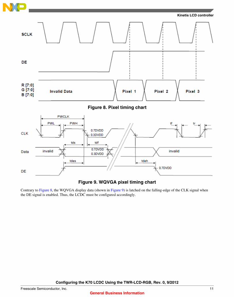
Figure 8. Pixel timing chart
Figure 9. WQVGA pixel timing chart
Contrary to Figure 8, the WQVGA display data (shown in Figure 9) is latched on the falling-edge of the CLK signal whenthe DE signal is enabled. Thus, the LCDC must be configured accordingly.
Kinetis LCD controller
Configuring the K70 LCDC Using the TWR-LCD-RGB, Rev. 0, 9/2012
Freescale Semiconductor, Inc. 11General Business Information

Figure 10. LCDC interface timing for 24-bit data active matrix color panels
Figure 10 shows the LCD interface timing generated by the K70 LCDC for an active matrix color TFT panel. In this figure,signals are shown with negative polarity. In TFT mode, LSCLK is automatically inverted. The panel interface timing foractive matrix panels is sometimes referred to as a "digital CRT" and is controlled by shift clock (LSCLK), horizontal sync
Kinetis LCD controller
Configuring the K70 LCDC Using the TWR-LCD-RGB, Rev. 0, 9/2012
12 Freescale Semiconductor, Inc.General Business Information

pulse (HSYNC, LP pin in passive mode), vertical sync pulse (VSYNC, FLM pin in passive mode), output enable (OE, ACDpin in passive mode), and line data (LD) signals. The following steps define the sequence of events for active matrix interfacetiming.
1. LSCLK latches data into the panel on its negative edge (when positive polarity is selected). In active mode, LSCLKruns continuously.
2. HSYNC causes the panel to start a new line.3. VSYNC causes the panel to start a new frame. It always encompasses at least one HSYNC pulse.4. OE functions as an output enable signal to the CRT. This signal is similar to blanking output in a CRT and enables the
data to be shifted onto the display. When disabled, data is invalid and the trace is off.
In a 24-bit color scheme, colors are defined as follows:• LD[23:16] bits define red.• LD[15:8] bits define green.• LD[7:0] bits define blue.
3.2.3 Custom LCD timingReset
Many LCD panels include an LCD controller which needs an external system reset. If an LCD needs this signal, the timingfor this pulse must also be found out. See the following figure.
Figure 11. Reset signal example
Table 6. LCD controller reset timing
Parameter Symbol Min. Typ. Max. Unit
Reset width TRW 15 - - ns
Reset rising time TRR - 10 ns
According to Figure 11, the RESET signal is active-low.
For the RESET signal to be at a logic High level during normal operation, it must be at least 15 ns in a Low state to beconsidered as a valid reset. Finally, according to Figure 11, the rising time of the signal is 10 ns, and for this reason, it is notrecommended to use an RC circuit to provide this signal.
Serial command interface
Generally, active matrix LCD displays have a more complex structure than passive displays requiring initialization andpower ON/OFF sequences. In order to be configured, these displays feature a serial interface, which uses either I2C or SPIprotocol as a standard.
Kinetis LCD controller
Configuring the K70 LCDC Using the TWR-LCD-RGB, Rev. 0, 9/2012
Freescale Semiconductor, Inc. 13General Business Information

Figure 12. SPI command interface timing chart exampe
WQVGA (800x600) SPI timing chart
The display power ON/OFF and initialization sequences are programmed via SPI interface. The following figure shows theWQVGA SPI timing chart.
Figure 13. WQVGA [800x600] SPI timing chart
The signal timings required to configure the display via SPI are shown in the following table:
Table 7. SPI signal timings
Item Symbol Min. Typ. Max. Unit
Serial Fclk fclk - - 20 MHz
Serial clk cycle time tclk 50 - - ns
Clk low width tsl 25 - - ns
Clk high width tsh 25 - - ns
Chip select setup time tcss 0 - - ns
Chip select hold time tcsh 10 - - ns
Chip select high delaytime
tcsd 20 - - ns
Data setup time tds 5 - - ns
Data hold time tdh 10 - - ns
Kinetis LCD controller
Configuring the K70 LCDC Using the TWR-LCD-RGB, Rev. 0, 9/2012
14 Freescale Semiconductor, Inc.General Business Information

Power ON/OFF sequence
To prevent the device damage from latch-up or DC operation, the power ON/OFF sequence shall be as shown in thefollowing figure.
Figure 14. Power ON/OFF sequence chart
Table 8. Power ON/OFF sequence timing
Parameter Specification Unit
T1 10 < T1 µs
T2 10 < T2 µs
T3 1 < T3 µs
• When DISP pin is pulled “H” (logic High state), blank data is output for 10 frames first, from the falling-edge of thefollowing VS signal.
• When DISP is pulled “L” (logic Low state), 10 frames of blank data will be output from the falling-edge of thefollowing VS, too.
Kinetis LCD controller
Configuring the K70 LCDC Using the TWR-LCD-RGB, Rev. 0, 9/2012
Freescale Semiconductor, Inc. 15General Business Information

3.3 LCD panels supported by K70TWR-LCD-RGB
Currently, only the TWR-LCD-RGB display is fully supported by the K70 LCDC module. Although planning is underway toadd more panels, it does not mean the module can only interact with that specific display (43WQW3T—4.3” WQVGA(480RGB x 272) TFT with Touch-Panel from Seiko Instruments Inc.). The user might develop his own interface with anydesired display as long as the control signals and timing parameters of such display comply with those on the K70 LCDC.
4 Graphics FrameWorks (GUI)
4.1 eGUIThe complimentary Freescale embedded graphical user interface (eGUI) allows single chip microcontroller (MCU) systemsto implement a graphical user interface and drive the latest generation of color graphics LCD panels with integrated displayRAM and simple serial peripheral interface (SPI) or parallel bus interface. The evolution of LCD panels integrating thedisplay RAM and LCD controller means that the products can be easily implemented without the need for a conventionalmicroprocessor (MPU) with integrated LCD driver hardware and external display RAM. The eGUI has also been expandedto support conventional LCD panels and ColdFire LCD MPUs, giving a complimentary entry level solution for theseplatforms. To support the eGUI, Freescale also provides a "converter utility" to change graphical bit maps and fonts into the"C" language arrays needed by the eGUI. The features of the eGUI/D4D are as follows.
Features
The eGUI/D4D is capable of generating the user menu, graphics, pictures, text, and display them on the LCD module. Itallows interacting with all objects, dynamically changing, adding, or removing them. It can also read and write their status orcurrent value. The D4D also fully supports touch screen capabilities of the LCD displays.
• Supports graphical color LCD displays of various sizes• Small RAM (volatile) memory footprint• Multiple platform support• Object style of driver• Smart support-screen-oriented structure of the user code• Custom screen sizes, position, and a header like window• Objects:
• Button• Check Box• Gauge• Icon• Label• Menu• Picture• Slider• Graph• Scroll Bar• Console• Text Bar
• Touch screen support• Multiple font support• Buffer for input keys
Graphics FrameWorks (GUI)
Configuring the K70 LCDC Using the TWR-LCD-RGB, Rev. 0, 9/2012
16 Freescale Semiconductor, Inc.General Business Information

Structure of an eGUI/D4D project
The following figure indicates the position of the D4D in the whole project. It is placed between the low-level drivers of theLCD and the user application.
Figure 15. eGUI/D4D project structure
Since this application note is aimed to develop a simple eGUI example, assuming that the user is already familiar with the filestructure and eGUI environment, only a brief description of its features is given. For basics and more detailed description oneGUI, see DRM116: Freescale Embedded GUI (D4D), available at freescale.com.
Hardware interface
Since the K70 features a dedicated data bus for the display control, unlike the preceding microcontrollers from the Kinetisand ColdFire family, which need to route the LCD data through the FlexBus, there is no need to configure the bus, though itis necessary to enable Port F Alternate Functions [ALT5 ] in the Configuration Register PORTF_PCR.
SPI for LCD Display
The LCD display requires a 4-wire SPI interface comprising of the following signals: SCK, CS, SDI, and SDO:
Figure 16. K70– LCD interface
When CS enables the communication [ LOW ], DSI is shifted into a 16-bit register on every SCK falling edge in an MSB bitfirst, the register-data differentiation is performed by a pair of bits sent before the SDO enablement [ LOW ]. CS can becontrolled by using either SPI_CS or a GPIO pin.
Graphics FrameWorks (GUI)
Configuring the K70 LCDC Using the TWR-LCD-RGB, Rev. 0, 9/2012
Freescale Semiconductor, Inc. 17General Business Information

Touch screen interface
The WQVGA dispay in TWR-LCD-RGB features an overlay resistive touch panel. It is a 4-wire resistive touch screen.Figure 17 shows its basic structure.
Figure 17. Basic touch screen structure
The touch screen is composed by two plastic films, each coated with a conductive layer of metal (usually indium tin oxide,ITO) separated by an air gap. One plate, X-plate (see Figure 17), is excited by the supply voltage. When the screen istouched, the two conductive plates come together, creating a resistor divider along the X-plate. The voltage at the point ofcontact, which represents the position on the X-plate, is sensed through the Y+ electrode, as shown in Figure 18. The processis then repeated by exciting the Y-plate and sensing the Y position through the X+ electrode.
Graphics FrameWorks (GUI)
Configuring the K70 LCDC Using the TWR-LCD-RGB, Rev. 0, 9/2012
18 Freescale Semiconductor, Inc.General Business Information

Figure 18. Position measurement
So, two ADC channels can be used with the GPIO pin multiplexed and two GPIO pins to simulate a touch screen controller.According to Figure 18 :
X position:1. Drive HIGH on X+ and drive LOW on X-, set Y- to HIGH-Z (may set it as input port).2. Set Y+ as ADC channel, then the user can read raw X voltage value from Y+.
Y position:1. Drive HIGH on Y+ and drive LOW on Y-, set X- to HIGH-Z (may set it as input port).2. Set X+ as ADC channel, then the user can read raw Y voltage value from X+.
However, this is just an example. The user can also use Y-/X- to read X/Y position. It is important to set another side (Y+/X+) to HIGH-Z to avoid reading a wrong value. After getting the raw voltage value, the X/Y position can be calculated withthe equation given below.
4.1.1 CodeWarrior projectFollow these steps to load the example code in CodeWarrior:
1. Download the eGUI from freescale.com/eGUI and unzip it, it will create a folder with the demo projects and anotherwith the D4D files.
2. Open the IDE. Choose File > Import > Existing projects into workspace. See Figure 19.
Graphics FrameWorks (GUI)
Configuring the K70 LCDC Using the TWR-LCD-RGB, Rev. 0, 9/2012
Freescale Semiconductor, Inc. 19General Business Information

Figure 19. Opening eGUI project in Codewarrior 13. Click Next, select the 'Select root directory' option and browse to the location where the demo project is located inside
the eGUI folder and click Finish. See Figure 20.
Graphics FrameWorks (GUI)
Configuring the K70 LCDC Using the TWR-LCD-RGB, Rev. 0, 9/2012
20 Freescale Semiconductor, Inc.General Business Information

Figure 20. Opening eGUI project in Codewarrior 2
4.1.2 eGUI configurationsBefore compiling, the user must configure the LCD and touch screen drivers according to the settings of the TWR-LCD-RGB board and controller module.
The eGUI LCD configuration headers set the low-level driver structure and the LCD hardware interface driver, in this case,the K70 LCDC.
d4d_user_cfg.h:
/**************************************************************//*!** Low Level driver specification for LCD display and optionally * for a touch screen interface*******************************************************************/
// Please define a used low LCD driver#define D4D_LLD_LCD d4dlcd_frame_buffer // the name of low level driver descriptor structure
// Please (if it's needed) define a used LCD hw interface driver#define D4D_LLD_LCD_HW d4dlcdhw_k70_lcdc
/**************************************************************//*!*
Graphics FrameWorks (GUI)
Configuring the K70 LCDC Using the TWR-LCD-RGB, Rev. 0, 9/2012
Freescale Semiconductor, Inc. 21General Business Information

* Touch screen low level driver section*******************************************************************/
// Please (if needed) define a used touch screen hw interface driver
#define D4D_LLD_TCH d4dtch_cr_touch
In order to make the LCDC interface with the display, configure all the screen parameters like height and width, type, cursor,color scheme and configuration registers; all this information must be included in the module’s header:
d4dlcdhw_k70_lcdc_cfg.h
#ifndef __D4DLCDHW_K70_LCDC_CFG_H#define __D4DLCDHW_K70_LCDC_CFG_H
/****************************************************************************** * includes ******************************************************************************/ // include here what the driver needs to run i.e.: "derivative.h" #include "MK70F15.h"
/****************************************************************************** * Constants ******************************************************************************/ #include "d4d.h" // include of all public items (types, function etc) of D4D driver#include "d4d_lldapi.h" // include non public low level driver interface header file #include "d4d_private.h" // include the private header file that contains perprocessor macros as D4D_MK_STR
// identification string of driver - must be same as name D4DTCH_FUNCTIONS structure + "_ID"// it is used for enable the code for compilation
#define d4dlcdhw_k70_lcdc_ID 1#if (D4D_MK_STR(D4D_LLD_LCD_HW) == d4dlcdhw_k70_lcdc_ID) // include of low level driver header file #include "d4dlcdhw_k70_lcdc.h"
/**************************************************************//*! * * Functions bodies * ******************************************************************/
static unsigned char D4DLCDHW_Init_K70LCDC(void){#ifdef TWRLCDRGB_REVA /* Initialize LCD Screen over SPI */ lcdc_init_spi_lcd(); // to do rewrite this part to any universal scheme#endif /* Setup LCD pin muxing */ lcdc_init_pins(); #if D4DLCDHWFB_MIRROWED == 1 LCDC_LSSAR = D4DLCDHWFB_START_ADDRESS + D4DLCDHWFB_X_MAX * D4DLCDHWFB_Y_MAX * 2; #else LCDC_LSSAR = D4DLCDHWFB_START_ADDRESS;
Graphics FrameWorks (GUI)
Configuring the K70 LCDC Using the TWR-LCD-RGB, Rev. 0, 9/2012
22 Freescale Semiconductor, Inc.General Business Information

#endif LCDC_LSR = (D4DLCDHWFB_X_MAX / 16) << 20 | (D4DLCDHWFB_Y_MAX); LCDC_LVPWR = (D4DLCDHWFB_X_MAX / 2); //LCDC_LDCR = ( 0| LCDC_LDCR_HM(4)| LCDC_LDCR_TM(8) ); //Configure_Bursting(); // set LCD virtual page width LCDC_LVPWR = LCDC_LVPWR_VPW( D4DLCDHWFB_X_MAX );
// set LCD cursor positon & settings (turn off) LCDC_LCPR = 0; LCDC_LCWHB = 0;
#ifdef TWRLCDRGB_REVA // set LCD panel configuration LCDC_LPCR = LCDC_LPCR_TFT_MASK | //TFT Screen LCDC_LPCR_COLOR_MASK | //Color LCDC_LPCR_BPIX(D4DLCDHWFB_BPP) | //bpp //LCDC_LPCR_PIXPOL_MASK | // pixel polarity LCDC_LPCR_FLMPOL_MASK | //first line marker active low LCDC_LPCR_LPPOL_MASK | //line pulse active low //LCDC_LPCR_END_SEL_MASK | //Use big-endian mode (0xFFAA5500 means R=AA,G=55,B=00) LCDC_LPCR_SWAP_SEL_MASK | LCDC_LPCR_SCLKIDLE_MASK | //Enalbe LSCLK when vsync is idle LCDC_LPCR_SCLKSEL_MASK | //Always enable clock LCDC_LPCR_ACD(ACD_DIV_0) | LCDC_LPCR_PCD(D4DLCDHWFB_PANEL_CLKDIV); //Divide 120 PLL clock by (3+1)=4 to get 30 MHz clock
// set LCD horizontal configuration based on panel data
LCDC_LHCR = LCDC_LHCR_H_WIDTH(9) | //(9+1)=10 SCLK period for HSYNC activated LCDC_LHCR_H_WAIT_1(9) | //(9+1)=10 SCLK period between end of OE and beginning of HSYNCLCDC_LHCR_H_WAIT_2(56); //(56+3)=59 SCLK periods between end of HSYNC and beginning of OE
// set LCD vertical configuration based on panel data
LCDC_LVCR = LCDC_LVCR_V_WIDTH(15) | //15 SCLK period for VSYNC activated LCDC_LVCR_V_WAIT_1(15) | //15 SCLK period between end of OE and beginning of VSYNC LCDC_LVCR_V_WAIT_2(15); //15 SCLK periods between end of VSYNC and beginning of OE #else LCDC_LPCR = LCDC_LPCR_TFT_MASK | //TFT Screen LCDC_LPCR_COLOR_MASK | //Color LCDC_LPCR_BPIX(D4DLCDHWFB_BPP) | //bpp //LCDC_LPCR_PIXPOL_MASK | // pixel polarity LCDC_LPCR_FLMPOL_MASK | //first line marker active low LCDC_LPCR_LPPOL_MASK | //line pulse active low LCDC_LPCR_END_SEL_MASK | //Use big-endian mode (0xFFAA5500 means R=AA,G=55,B=00) //LCDC_LPCR_SWAP_SEL_MASK | LCDC_LPCR_SCLKIDLE_MASK | //Enable LSCLK when vsync is idle LCDC_LPCR_SCLKSEL_MASK | //Always enable clock LCDC_LPCR_CLKPOL_MASK | //Active on positive edge of LSCLK. In TFT mode, active on negative edge of LSCLK. // LCDC_LPCR_ACD(ACD_DIV_7) | // It isn't used in TFT mode LCDC_LPCR_PCD(12); //Divide 120 PLL clock by (12+1)=13 to get 9.23 MHz clock
Graphics FrameWorks (GUI)
Configuring the K70 LCDC Using the TWR-LCD-RGB, Rev. 0, 9/2012
Freescale Semiconductor, Inc. 23General Business Information

// set LCD horizontal configuration based on panel data
LCDC_LHCR = LCDC_LHCR_H_WIDTH(1) | //(1+1)=2 SCLK period for HSYNC activated LCDC_LHCR_H_WAIT_1(1) | //(1+1)=2 SCLK period between end of OE and beginning of HSYNC LCDC_LHCR_H_WAIT_2(38); //(38+3)=41 SCLK periods between end of HSYNC and beginning of OE
// set LCD vertical configuration based on panel data
LCDC_LVCR = LCDC_LVCR_V_WIDTH(2) | //2 SCLK period for VSYNC activated LCDC_LVCR_V_WAIT_1(2) | //2 SCLK period between end of OE and beginning of VSYNC LCDC_LVCR_V_WAIT_2(10); //10 SCLK periods between end of VSYNC and beginning of OE #endif // set LCD panning offset LCDC_LPOR = 0;
// set LCD interrupt configuration LCDC_LICR = 0; // set LCD interrupt enable LCDC_LIER = 0; //Set background plane DMA to burst mode LCDC_LDCR &= ~(LCDC_LDCR_BURST_MASK);
#if 0 // set LCD graphic window start address LCDC_LGWSAR = 0x80000000;
// set LCD graphic window size LCDC_LGWSR = LCDC_LGWSR_GWW(0) | LCDC_LGWSR_GWH(0);
// set LCD graphic window virtual page width LCDC_LGWVPWR = 0;
// set LCD graphic window panning offset LCDC_LGWPOR = 0;
// set LCD graphic window position LCDC_LGWPR = LCDC_LGWPR_GWXP(0) | LCDC_LGWPR_GWYP(0);
// set LCD graphic window control LCDC_LGWCR = LCDC_LGWCR_GWAV(0xF) | // alpha-transparent // (1 << LCDC_LGWCR_GWE_SHIFT) | // enable (1 << LCDC_LGWCR_GWCKE_SHIFT) | // color key enable LCDC_LGWCR_GWCKR(0xFF) | // color key LCDC_LGWCR_GWCKG(0) | LCDC_LGWCR_GWCKB(80); // LCDC_LAUSCR = LCDC_LAUSCR_AGWCKB_MASK;#endif /* Enable LCD */ SIM_MCR|=SIM_MCR_LCDSTART_MASK;
return 1;}
Graphics FrameWorks (GUI)
Configuring the K70 LCDC Using the TWR-LCD-RGB, Rev. 0, 9/2012
24 Freescale Semiconductor, Inc.General Business Information

} //-----------------------------------------------------------------------------// FUNCTION: D4DLCD_FlushBuffer_K70LCDC // SCOPE: Low Level Driver API function // DESCRIPTION: For buffered low level interfaces is used to inform the // driver the complete object is drawn and pending pixels should be flushed // // PARAMETERS: none // RETURNS: none //----------------------------------------------------------------------------- static void D4DLCD_FlushBuffer_K70LCDC(void) { //mcf5227_cache_invalidate(); }
static void lcdc_init_pins(void){ //#define ALT2 (0|PORT_PCR_MUX(2)|PORT_PCR_DSE_MASK) //#define ALT5 (0|PORT_PCR_MUX(5)|PORT_PCR_DSE_MASK) //#define ALT7 (0|PORT_PCR_MUX(7)|PORT_PCR_DSE_MASK) #define ALT1 (0|PORT_PCR_MUX(1)) #define ALT2 (0|PORT_PCR_MUX(2)) #define ALT5 (0|PORT_PCR_MUX(5)) #define ALT7 (0|PORT_PCR_MUX(7)) PORTF_PCR4 =ALT7; // Graphic LCD D[0], Schematic PTF4PORTF_PCR5 =ALT7; // Graphic LCD D[1], Schematic PTF5PORTF_PCR6 =ALT7; // Graphic LCD D[2], Schematic PTF6PORTF_PCR7 =ALT7; // Graphic LCD D[3], Schematic PTF7PORTF_PCR8 =ALT7; // Graphic LCD D[4], Schematic PTF8PORTF_PCR9 =ALT7; // Graphic LCD D[5], Schematic PTF9PORTF_PCR10=ALT7; // Graphic LCD D[6], Schematic PTF10PORTF_PCR11=ALT7; // Graphic LCD D[7], Schematic PTF11
PORTF_PCR12=ALT7; // Graphic LCD D[8], Schematic PTF12PORTF_PCR13=ALT7; // Graphic LCD D[9], Schematic PTF13PORTF_PCR14=ALT7; // Graphic LCD D[10], Schematic PTF14PORTF_PCR15=ALT7; // Graphic LCD D[11], Schematic PTF15PORTF_PCR16=ALT5; // Graphic LCD D[12], Schematic PTF16PORTF_PCR17=ALT5; // Graphic LCD D[13], Schematic PTF17PORTF_PCR18=ALT5; // Graphic LCD D[14], Schematic PTF18PORTF_PCR19=ALT5; // Graphic LCD D[15], Schematic PTF19
PORTF_PCR20=ALT5; // Graphic LCD D[16], Schematic PTF20PORTF_PCR21=ALT7; // Graphic LCD D[17], Schematic PTF21PORTF_PCR22=ALT7; // Graphic LCD D[18], Schematic PTF22PORTF_PCR23=ALT7; // Graphic LCD D[19], Schematic PTF23PORTF_PCR24=ALT7; // Graphic LCD D[20], Schematic PTF24PORTF_PCR25=ALT7; // Graphic LCD D[21], Schematic PTF25
PORTF_PCR26=ALT7; // Graphic LCD D[22], Schematic PTF26PORTF_PCR27=ALT7; // Graphic LCD D[23], Schematic PTF27
PORTF_PCR0=ALT7; // Graphic LCD PCLK, Schematic PTF0PORTF_PCR1=ALT7; // Graphic LCD DE, Schematic PTF1PORTF_PCR2=ALT7; // Graphic LCD HSYNC, Schematic PTF2PORTF_PCR3=ALT7; // Graphic LCD VSYNC, Schematic PTF3
Graphics FrameWorks (GUI)
Configuring the K70 LCDC Using the TWR-LCD-RGB, Rev. 0, 9/2012
Freescale Semiconductor, Inc. 25General Business Information

5 PEG+This part of the document describes steps required to configure the IAR Embedded Workbench for ARM® development tooland use it to build, run, and debug PEG+ applications for the TWR-K60N512 board. This document also provides board-specific information related to the PEG.
NOTEC/PEG, PEG+, PEG PRO and IAR are third-party applications, the code exampledepicted and included in this document does not grant access rights nor does it license theusage of any of the above mentioned products, henceforth proper software and/or licensemust be acquired by the developers at their own cost.
Fore more information on PEG+, see swellsoftware.com/products/pegplus.php.
5.1 Requirements to run the code example• IAR Embedded Workbench for ARM: IAR Embedded Workbench for ARM must be installed on the computer. If
not, download the latest version from the IAR website: iar.com• Freescale MQX™ RTOS: Freescale MQX RTOS operating system must be installed on the computer. If not,
download the last version from the Freescale website: freescale.com/MQX• PE micro OSBDM Drivers: The P&E OSDBM drivers have to be installed in order to download and debug the PEG+
application. If not, download the latest version from PEmicro website: pemicro.com/osbdm• PEG supports a wide range of platforms and CPUs, but this document focuses on PEG+ running on the Tower board
TWR-K70F120M with its TWR-LCD peripheral module. For more details, see the Freescale Tower website:freescale.com/TWR-K70F120M
5.2 Building PEG+ application
5.2.1 Building the MQX librariesFor more information, see C:\Program Files\IAR Systems\Embedded Workbench 6.4\ARM\RTOS\FreescaleMQX.
5.2.2 Compile-time configurationMajor compile-time configuration options are centralized in a single user configuration file located in
<mqx_path>/config/twrk70f120m/user_config.h. See the following figure.
This user configuration file is included internally by private configuration files in MQX PSP and BSP projects.
NOTEBSPCFG_ENABLE_CPP option must be enabled in the user_config.h file.
PEG+
Configuring the K70 LCDC Using the TWR-LCD-RGB, Rev. 0, 9/2012
26 Freescale Semiconductor, Inc.General Business Information

5.2.3 Build processAfter any change to the compile-time user configuration file or MQX kernel source files, the MQX libraries need to berebuilt. The build process is similar with all core components:
• The output directory are <mqx_path>/lib/twrk70f120m.iar/bsp and <mqx_path>/lib/twrk60n512.iar/psp.
• All public header files needed by application to make use of the library are automatically copied from internal foldersto the same output directory as the library itself.
• During PSP or BSP build process, the user_config.h file and other header files from the <mqx_path>/ config/twrk70f120m and config/common directories are copied into the <mqx_path>/ lib/twrk70f120m.iar outputdirectory.
With IAR, the MQX build process can be simplified by using the Batch Build feature. For each supported board, there is anIAR Workspace file which includes build projects for all related MQX libraries:
<mqx_path>/config/twrk60n512/iar/build_libs.eww
The Workspace file contains Batch Build configurations which can be used to build all MQX libraries at once. See thefollowing figure.
PEG+
Configuring the K70 LCDC Using the TWR-LCD-RGB, Rev. 0, 9/2012
Freescale Semiconductor, Inc. 27General Business Information

5.2.4 Building the PEG+ example Hellopeg
5.2.4.1 MQX Project pathThe hellopeg project is prepared using a Windows System variable called MQX_PATH. So, before starting the hellopeg IARproject:
From Control panel, choose System Properties > Advanced Tab -> Environment Variables to set the MQX_PATH variable tothe location where Freescale MQX RTOS is installed. See the following figure.
PEG+
Configuring the K70 LCDC Using the TWR-LCD-RGB, Rev. 0, 9/2012
28 Freescale Semiconductor, Inc.General Business Information

5.2.4.2 Importing hellopeg IAR projectIn order to compile the hellopeg example, the project has to be opened into IAR. From Menu, choose File > Open workspace,then File > Open file and navigate through the example folder (See the following figure). Select and import the followingprojects.
• hellopeg project:
<peg_path>\examples\plus\480x272\hellopeg\build_twrk70f120m-iar-mqx-d\iar
PEG+
Configuring the K70 LCDC Using the TWR-LCD-RGB, Rev. 0, 9/2012
Freescale Semiconductor, Inc. 29General Business Information

5.2.4.3 Building the hellopeg IAR projectSelect hellopeg project, right-click and then press Rebuild All or the Make button. See the following figure.
NOTECurrently only one configuration is available, FLASH_1M_PFLASH.
5.2.4.4 Downloading and debugging the hellopeg IAR projectIn order to download and debug the PEG+ application, just press the Download and Debug button.
The debug configuration is already set for the USB/OSBDM interface (PEMicro). See the following figure.
PEG+
Configuring the K70 LCDC Using the TWR-LCD-RGB, Rev. 0, 9/2012
30 Freescale Semiconductor, Inc.General Business Information

After the application is downloaded, the PEG+ hellopeg application is ready to run.
6 Example
6.1 Register configurationThis section discusses how to configure the LCD controller registers necessary to establish:
• Screen size• Display properties
• Cursor properties• Color space• Contrast
6.2 Screen sizeThe first parameter to be defined is the screen size; this information cannot be randomly selected, it must concur with thescreen size depicted in the datasheet of the display. In this specific case, the screen size is 480x272.
LCDC_LSSAR LCDC Screen Start Address Register
This register specifies the LCD screen start address.
LCDC_LSSAR = D4DLCDHWFB_START_ADDRESS;
Defined in the header file as: D4DLCDHWFB_START_ADDRESS= 0x80000000
LCDC_LSR LCDC Size Register
Table continues on the next page...
Example
Configuring the K70 LCDC Using the TWR-LCD-RGB, Rev. 0, 9/2012
Freescale Semiconductor, Inc. 31General Business Information

This register defines the height and width of the LCD screen defined in its datasheet.
LCDC_LSR = (D4DLCDHWFB_X_MAX / 16) << 20 | (D4DLCDHWFB_Y_MAX);
Defined in the header file as: D4DLCDHWFB_X_MAX= 480D4DLCDHWFB_Y_MAX= 272
LCDC_LVPWR LCDC Virtual Page Width Register
This register defines virtual page width for LCD panel. Refer to LCD screen format for more details.
LCDC_LVPWR = (D4DLCDHWFB_X_MAX / 2);
6.3 Display propertiesOnce the screen size has been defined, the user must establish the display properties such as screen type (TFT/color), cursorheight, width, color, blink and starting position. All the cursor properties except the starting position are aesthetic choices; thecursor starting position indicates where the graphics will start being “drawn” on the screen.
LCDC_LCPR
LCDC_LCPR = 0;
LCDC Cursor Position Register
This register determines the starting position of the cursor on the LCD panel
LCDC_LCWHB
// set LCD cursor positon & settings (turn off)LCDC_LCWHB = 0;
LCDC Cursor Width, Height, and Blink Register
This register determines the cursor’s width and height, and how it blinks
LCDC_LCCMR LCDC Color Cursor Mapping register
This register defines the cursor color in passive or TFT color modes. If bpp mode setting is smaller than 18bpp, cursor color component bits must be put in the MSBs
The next step is to define the color space, scheme or depth which specifies the number of available colors. If the color depthis higher, the number of colors available to display graphics or text, would be more. It also defines how many physical linesof the LCDC controller will be used to feed the LCD screen. For this example, the highest color depth was chosen (24bpp),thus the 24 lines (8 lines/color) of the LCDC bus will be used.
LCDC_LPCR LCDC Panel Configuration Register
This register defines all properties of the LCD screen.
LCDC_LPCR =
LCDC_LPCR_TFT_MASK | //TFT Screen
LCDC_LPCR_COLOR_MASK | //Color
LCDC_LPCR_BPIX(D4DLCDHWFB_BPP) | //bpp
Table continues on the next page...
Example
Configuring the K70 LCDC Using the TWR-LCD-RGB, Rev. 0, 9/2012
32 Freescale Semiconductor, Inc.General Business Information

LCDC_LPCR_FLMPOL_MASK | //first line marker active low
LCDC_LPCR_LPPOL_MASK | //line pulse active low
LCDC_LPCR_SWAP_SEL_MASK |
LCDC_LPCR_SCLKIDLE_MASK | //Enable LSCLK when vsync is idle
LCDC_LPCR_SCLKSEL_MASK | //Always enable clock
LCDC_LPCR_ACD(ACD_DIV_0) |
LCDC_LPCR_PCD(D4DLCDHWFB_PANEL_CLKDIV);
//Divide 120 PLL clock by (3+1)=4 to get 30 MHz clock
Defined in the header file as:
D4DLCDHWFB_BPP_BYTE 4
D4DLCDHWFB_BPP BPP24= 7
D4DLCDHWFB_PANEL_CLKDIV 3
6.4 Display horizontal and vertical controlNow that the screen properties have been defined, the horizontal and vertical configuration registers must be configured,these values must be taken from the display’s datasheet since they define the CLK periods the controller will use to “draw”the graphics.
LCDC_LHCR LCDC Horizontal Configuration Register
This register defines the horizontal sync pulse timing. Defined by the displays properties.
// set LCD horizontal configuration based on panel data (See Seiko Datasheet)
LCDC_LHCR =
LCDC_LHCR_H_WIDTH(9) | //(9+1)=10 SCLK period for HSYNC activated
LCDC_LHCR_H_WAIT_1(9) | //(9+1)=10 SCLK period between end of OE and beginning ofHSYNC
LCDC_LHCR_H_WAIT_2(56); //(56+3)=59 SCLK periods between end of HSYNC andbeginning of OE
LCDC_LVCR LCDC Vertical Configuration Register
This register defines the vertical sync pulse timing. Defined by the displays properties
LCDC_LVCR =
LCDC_LVCR_V_WIDTH(15) | //15 SCLK period for VSYNC activated
LCDC_LVCR_V_WAIT_1(15) | //15 SCLK period between end of OE and beginning ofVSYNC
Table continues on the next page...
Example
Configuring the K70 LCDC Using the TWR-LCD-RGB, Rev. 0, 9/2012
Freescale Semiconductor, Inc. 33General Business Information

LCDC_LVCR_V_WAIT_2(15); //15 SCLK periods between end of VSYNC and beginning ofOE
LCDC_LPOR LCDC Panning Offset Register
This register sets up panning for the image.
LCDC_LPOR = 0;
6.5 Display contrast and brightnessAfter setting up the horizontal and vertical signals we need to define the display contrast and brightness, interrupt settings andgraphic windows size.
LCDC_LPCCR LCDC PWM Contrast Control Register
This register controls the signal output at the contrast pin controlling the display’s contrast.
LCDC_LDCR
//Set background plane DMA to burst mode LCDC_LDCR & = ~ (LCDC_LDCR_BURST_MASK);
LCDC DMA Control Register
There is a 128 x 32 bit line buffer in the LCDC that stores DMA data from system memory. LDCR controls DMA burst length and when to trigger a DMA burst in terms of number of data bytes left in the pixel buffer.
LCDC_LICR
LCDC_LICR = 0;
LCDC Interrupt Configuration Register
This register configures the interrupt conditions.The LCDC selects between triggering an interrupt at either the End of Frame or at the Beginning of Frame. This register works in conjunction with the LIER to enable LCDC interrupts.
LCDC_LIER
LCDC_LIER = 0;
LCDC Interrupt Enable Register
This register enables the LCDC to generate an interrupt. When the interrupt is disabled, its status can still be observed in the Interrupt Status Register.
LCDC_LGWSAR
LCDC_LGWSAR = 0x80000000;
LCDC Graphic Window Start Address Register
This register defines the starting address of the graphic window image
Table continues on the next page...
Example
Configuring the K70 LCDC Using the TWR-LCD-RGB, Rev. 0, 9/2012
34 Freescale Semiconductor, Inc.General Business Information

LCDC_LGWSR
LCDC_LGWSR = LCDC_LGWSR_GWW(0); LCDC_LGWSR_GWH(0);
LCDC Graphic Window Size Register
This register defines the height and width of the graphic window on the LCD screen.
LCDC_LGWVPWR
LCDC_LGWVPWR = 0;
LCDC Graphic Window Virtual Page Width Register
This register defines the virtual page width for the graphic window picture on the LCD screen.
LCDC_LGWPOR
// set LCD graphic window panning offset LCDC_LGWPOR = 0;
LCDC Graphic Window Panning Offset Register
This register sets up panning for the graphic window.
LCDC_LGWPR
// set LCD graphic window position LCDC_LGWPR = LCDC_LGWPR_GWXP(0) | LCDC_LGWPR_GWYP(0);
LCDC Graphic Window Position Register
This register determines the starting position of the graphic window on the LCD panel.
LCDC_LGWCR
// set LCD graphic window control
LCDC_LGWCR =LCDC_LGWCR_GWAV(0xF) |(1 << LCDC_LGWCR_GWCKE_SHIFT) |LCDC_LGWCR_GWCKR(0xFF) |LCDC_LGWCR_GWCKG(0) |LCDC_LGWCR_GWCKB(80);
LCDC Graphic Window Control Register
This register defines the behaviors of graphic window.
// alpha-transparent // color key enable // color key
7 Code
7.1 eGUI Code/* * File:Game.c * Purpose:Main process * */#include "main.h"
Code
Configuring the K70 LCDC Using the TWR-LCD-RGB, Rev. 0, 9/2012
Freescale Semiconductor, Inc. 35General Business Information

#include "common.h"#include "mcg.h"#include "pit.h"#include "isr.h"#include "d4d.h"volatile LWord free_counter2ms = 0;D4D_EXTERN_SCREEN(screen_entry);
/**************************************************************//*!** Global variables*******************************************************************/
TIME_FLAGS time;LWord time100sm_cnt = 0;
/**************************************************************//*!* Prototypes ******************************************************************/static void pit_ch0_callback(void);void MCU_Init(void);void Timer_Init(void);/**************************************************************//*!* Module Global Variables******************************************************************/short int value;volatile unsigned char value_msb;volatile unsigned char value_lsb;char Acceleration[6];volatile unsigned char Read_End=0;volatile unsigned char Enable_Acc=0;
/**************************************************************//*!* Init Clock and PLL ******************************************************************/void MCU_Init(void){ volatile int fmc_pfb01cr_register, fmc_pfb23cr_register; #define _CACHE_ON_ #ifdef _CACHE_ON_ // turn code cache on LMEM_PCCCR = (LMEM_PCCCR_GO_MASK | LMEM_PCCCR_INVW1_MASK | LMEM_PCCCR_INVW0_MASK | LMEM_PCCCR_ENWRBUF_MASK | LMEM_PCCCR_ENCACHE_MASK);while( LMEM_PCCCR & LMEM_PCCCR_GO_MASK ){};#endif // Enable IPF/DPF/IC/DCFMC_PFB01CR ^= 0x00000001F;FMC_PFB23CR ^= 0x00000001F; // Enable IPF/DPF/IC/DC/**************************************************************//*!* Module Global Variables******************************************************************/short int value;volatile unsigned char value_msb;volatile unsigned char value_lsb;char Acceleration[6];volatile unsigned char Read_End=0;volatile unsigned char Enable_Acc=0;
/**************************************************************//*!* Init Clock and PLL ******************************************************************/void MCU_Init(void){ volatile int fmc_pfb01cr_register, fmc_pfb23cr_register; #define _CACHE_ON_ #ifdef _CACHE_ON_
Code
Configuring the K70 LCDC Using the TWR-LCD-RGB, Rev. 0, 9/2012
36 Freescale Semiconductor, Inc.General Business Information

// turn code cache on LMEM_PCCCR = (LMEM_PCCCR_GO_MASK | LMEM_PCCCR_INVW1_MASK | LMEM_PCCCR_INVW0_MASK | LMEM_PCCCR_ENWRBUF_MASK | LMEM_PCCCR_ENCACHE_MASK);while( LMEM_PCCCR & LMEM_PCCCR_GO_MASK ){};#endif // Enable IPF/DPF/IC/DCFMC_PFB01CR ^= 0x00000001F;FMC_PFB23CR ^= 0x00000001F; // Enable IPF/DPF/IC/DC if(flags.bits.b100ms) time100sm_cnt++; }}
/********************************************************************/
7.2 PEG+ code#include "peg.hpp"
#ifdef PEGMQXextern void PegTaskMain(uint_32);
TASK_TEMPLATE_STRUCT MQX_template_list[] ={ {PEG_TASK_ID, PegTaskMain, PEG_STACK_SIZE, PEG_PRIORITY, "PegTask", MQX_AUTO_START_TASK, 0, 0}, {0, 0, 0, 0, 0, 0, 0, 0}};#endif
PEGCHAR Hello[] = {'H','E','L','L','O', 0};PEGCHAR Day[] = {'H','a','v','e',' ','a',' ','n','i','c','e',' ','d','a','y', 0};
8 Appendix AUsing different LCD screens
The fact that the only LCD screen depicted in this application note is a Seiko 4.3" WQVGA (800x600) 24-bit TFT LCDdisplay and no other display is mentioned does not mean the K70 LCDC module does not support different screens; theregister settings can be modified to use different screens as long as they comply with the LCDC module parameters.
Industrial applications: Screen and controller physically separated
Industrial control applications often require a graphic control module separated from the control module by more than a fewinches which makes the interface development difficult, in those cases there are a couple of workarounds, depending on howcost sensitive the application is, that is,
• For example, consider a scenario where the graphic control module (display) must be 6 ft. away from the controlmodule (K70). The question arises whether a simple cable can be used to communicate to both.
The answer is must definitely no, the signal strength will be almost completely attenuated to a point the display willrecognize the signals as noise.
A possible solution would be to configure the LCDC to work on a VGA resolution and use a VGA cable. The drawback ofthis solution would be the inability to use the touchscreen functionality; unless a separate cable was used to feed the K70’sADC and even then an instrumentation amplifier would be necessary in order to amplify the touchscreen signals so the ADCcould recognize and validate them.
Appendix A
Configuring the K70 LCDC Using the TWR-LCD-RGB, Rev. 0, 9/2012
Freescale Semiconductor, Inc. 37General Business Information

• The second question is how to achieve the link between the two modules.
If cost is not a problem, a K61 which has the same functionality, package and GPIOs with the exception of the LCDC modulecould be used as the controller module. Then, a SPI communication link could be established to a K70 placed at the samelocation the LCD screen is, feeding the K70 with the real time operations, allowing the K70 to manage the graphic-touchscreen interface. The main drawback is its cost.
Appendix A
Configuring the K70 LCDC Using the TWR-LCD-RGB, Rev. 0, 9/2012
38 Freescale Semiconductor, Inc.General Business Information
How to Reach Us:
Home Page:www.freescale.com
Web Support:http://www.freescale.com/support
USA/Europe or Locations Not Listed:Freescale SemiconductorTechnical Information Center, EL5162100 East Elliot RoadTempe, Arizona 85284+1-800-521-6274 or +1-480-768-2130www.freescale.com/support
Europe, Middle East, and Africa:Freescale Halbleiter Deutschland GmbHTechnical Information CenterSchatzbogen 781829 Muenchen, Germany+44 1296 380 456 (English)+46 8 52200080 (English)+49 89 92103 559 (German)+33 1 69 35 48 48 (French)www.freescale.com/support
Japan:Freescale Semiconductor Japan Ltd.HeadquartersARCO Tower 15F1-8-1, Shimo-Meguro, Meguro-ku,Tokyo 153-0064Japan0120 191014 or +81 3 5437 [email protected]
Asia/Pacific:Freescale Semiconductor China Ltd.Exchange Building 23FNo. 118 Jianguo RoadChaoyang DistrictBeijing 100022China+86 10 5879 [email protected]
Document Number: AN4588Rev. 0, 9/2012
Information in this document is provided solely to enable system and softwareimplementers to use Freescale Semiconductors products. There are no express or impliedcopyright licenses granted hereunder to design or fabricate any integrated circuits orintegrated circuits based on the information in this document.
Freescale Semiconductor reserves the right to make changes without further notice to anyproducts herein. Freescale Semiconductor makes no warranty, representation, orguarantee regarding the suitability of its products for any particular purpose, nor doesFreescale Semiconductor assume any liability arising out of the application or use of anyproduct or circuit, and specifically disclaims any liability, including without limitationconsequential or incidental damages. "Typical" parameters that may be provided inFreescale Semiconductor data sheets and/or specifications can and do vary in differentapplications and actual performance may vary over time. All operating parameters,including "Typicals", must be validated for each customer application by customer'stechnical experts. Freescale Semiconductor does not convey any license under its patentrights nor the rights of others. Freescale Semiconductor products are not designed,intended, or authorized for use as components in systems intended for surgical implantinto the body, or other applications intended to support or sustain life, or for any otherapplication in which failure of the Freescale Semiconductor product could create asituation where personal injury or death may occur. Should Buyer purchase or useFreescale Semiconductor products for any such unintended or unauthorized application,Buyer shall indemnify Freescale Semiconductor and its officers, employees, subsidiaries,affiliates, and distributors harmless against all claims, costs, damages, and expenses, andreasonable attorney fees arising out of, directly or indirectly, any claim of personal injuryor death associated with such unintended or unauthorized use, even if such claims allegesthat Freescale Semiconductor was negligent regarding the design or manufacture ofthe part.
RoHS-compliant and/or Pb-free versions of Freescale products have the functionality andelectrical characteristics as their non-RoHS-complaint and/or non-Pb-free counterparts.For further information, see http://www.freescale.com or contact your Freescalesales representative.
For information on Freescale's Environmental Products program, go tohttp://www.freescale.com/epp.
Freescale™ and the Freescale logo are trademarks of Freescale Semiconductor, Inc.All other product or service names are the property of their respective owners.
© 2012 Freescale Semiconductor, Inc.