configurable hardware architectures for frequency …
TRANSCRIPT

CONFIGURABLE HARDWARE ARCHITECTURES FOR FREQUENCY
DIVERSE TARGET DETECTION
BY
JOSHUA WEBER
Submitted in partial fulfillment of therequirements for the degree of
Master of Science in Computer Engineeringin the Graduate College of theIllinois Institute of Technology
ApprovedAdvisor
Chicago, IllinoisMay 2008

c© Copyright by
JOSHUA WEBER
May 2008
ii

ACKNOWLEDGMENT
I would like to thank my academic advisors, Dr. Erdal Oruklu and Dr. Jafar
Saniie. They have provided invaluable guidance not only in the production of this
thesis but in guidance of my academic and career paths.
I’d like to further thank my girlfriend, Jennifer Keplinger, for not only the
support she has provided to me but also for challenging me to always be improving.
I’m ever grateful to my sister, Kali Weber, who has made my life a joy and
always provided me with the sense of a home filled with loving family.
And most importantly I’d like to thank my parents, Lon and Sharlene Weber,
who taught me to be the person I am today. With out you I would have never
learned the value of knowledge or developed the drive to always learn more. None of
my accomplishments could have been achieved without your support, I love you.
iii

TABLE OF CONTENTS
Page
ACKNOWLEDGEMENT . . . . . . . . . . . . . . . . . . . . . . . . . iii
LIST OF TABLES . . . . . . . . . . . . . . . . . . . . . . . . . . . . v
LIST OF FIGURES . . . . . . . . . . . . . . . . . . . . . . . . . . . . vi
ABSTRACT . . . . . . . . . . . . . . . . . . . . . . . . . . . . . . . vii
CHAPTER
1. INTRODUCTION . . . . . . . . . . . . . . . . . . . . . . . 1
1.1. Motivation . . . . . . . . . . . . . . . . . . . . . . . . 11.2. Significance of Work . . . . . . . . . . . . . . . . . . . 21.3. Organization . . . . . . . . . . . . . . . . . . . . . . . 3
2. SURVEY OF PRIOR WORK . . . . . . . . . . . . . . . . . 4
2.1. Introduction . . . . . . . . . . . . . . . . . . . . . . . 42.2. Split Spectrum Processing . . . . . . . . . . . . . . . . 4
3. ARCHITECTURAL DESIGN . . . . . . . . . . . . . . . . . 9
3.1. Pure Hardware Architecture . . . . . . . . . . . . . . . 93.2. Pure Software Architecture . . . . . . . . . . . . . . . . 15
4. IMPLEMENTATION DETAILS . . . . . . . . . . . . . . . . 18
4.1. General Implementation Details . . . . . . . . . . . . . . 184.2. Hardware Implementation . . . . . . . . . . . . . . . . . 204.3. Software Implementation . . . . . . . . . . . . . . . . . 27
5. EXPERIMENTAL RESULTS . . . . . . . . . . . . . . . . . 31
5.1. Experimental Test Configuration . . . . . . . . . . . . . 315.2. Flaw-To-Clutter Ratio Performance . . . . . . . . . . . . 325.3. Execution Time Results . . . . . . . . . . . . . . . . . . 375.4. Implimentation Area Results . . . . . . . . . . . . . . . 415.5. Design Space Considerations . . . . . . . . . . . . . . . 44
6. CONCLUSION . . . . . . . . . . . . . . . . . . . . . . . . 47
6.1. Concluding Remarks . . . . . . . . . . . . . . . . . . . 476.2. Future Work . . . . . . . . . . . . . . . . . . . . . . . 48
BIBLIOGRAPHY . . . . . . . . . . . . . . . . . . . . . . . . . . . . . 50
iv

LIST OF TABLES
Table Page
5.1 SSP Matlab simulation of 4 and 8 channels . . . . . . . . . . . . 33
5.2 Software Architecture Flow-To-Clutter Ratio . . . . . . . . . . . 34
5.3 Hardware Architecture Flaw-To-Clutter Ratio . . . . . . . . . . . 36
5.4 Software Architecture Execution Time . . . . . . . . . . . . . . 39
5.5 Hardware Architecture Execution Time . . . . . . . . . . . . . . 40
5.6 Software FPGA Resource Usage . . . . . . . . . . . . . . . . . . 42
5.7 Hardware FPGA Resource Usage . . . . . . . . . . . . . . . . . 43
v

LIST OF FIGURES
Figure Page
2.1 Split Spectrum Processing . . . . . . . . . . . . . . . . . . . . 5
2.2 Window Filter Placement . . . . . . . . . . . . . . . . . . . . 6
2.3 FCR improvement using Split Spectrum Processing . . . . . . . 8
3.1 Pure Hardware Architecture . . . . . . . . . . . . . . . . . . . 11
3.2 Signal Processing Module Block Diagram . . . . . . . . . . . . 13
3.3 User Interface Software Stack . . . . . . . . . . . . . . . . . . 14
4.1 Nallatech ExtremeDSP Development Kit-IV . . . . . . . . . . . 19
4.2 Memory Address Space . . . . . . . . . . . . . . . . . . . . . 22
4.3 Hardware Architecture Graphical User Interface . . . . . . . . . 27
4.4 Microblaze Soft Core Implementation . . . . . . . . . . . . . . 29
5.1 Experimental Test Setup . . . . . . . . . . . . . . . . . . . . 32
5.2 FCR Performance vs. Resource Usage . . . . . . . . . . . . . . 46
5.3 Execution Time vs. Resource Usage . . . . . . . . . . . . . . . 46
vi

ABSTRACT
Ultrasonic imaging has applications in many industries, such as non destructive
testing, medical imaging, and industrial applications. Previous research into ultra-
sonic imaging has focused on offline processing of echo data. A topic of increasing
interest is real-time processing of ultrasonic data.
Due to the microstructure of materials the echo signal contains a high amount
of clutter noise. In order to achieve target detection it is necessary to filter this
clutter noise. Split Spectrum Processing (SSP) has been demonstrated to excel at
filtering of clutter noise. While the SSP algorithm is able to achieve excellent filtering
performance it does so at a large computational complexity.
In order to produce a portable real time system the restrictions on process-
ing time and computational complexity must be overcome. The system-on-a-chip
(SOC) methodology is one such technique to achieve this. SOC attempts to com-
bine all system components on a single device to provide benefits in performance and
integration.
This paper will present two unique SOC based architectures for achieving
real-time SSP ultrasonic target detection. These two architectures will be design,
implemented, and tested. Discussion of the issues of implementation and performance
of the designs will be presented. The goal of this paper is to explore and quantify the
issues surrounding a reconfigurable hardware implementation for ultrasonic frequency
diverse target detection.
vii

1
CHAPTER 1
INTRODUCTION
1.1 Motivation
Ultrasonic target (flaw) detection has applications in many industries and fields
such as medical imaging, manufacturing, maintenance, and non destructive testing
[APR96, LV90]. One of the limiting factors in the application of ultrasonic target
detection is the presence of very high clutter noise. This high cluttering noise is very
detrimental to target detection, as it is often larger then the target echo itself. For
this reason, it is difficult to filter this clutter noise using simple signal processing
techniques [San81].
It has been demonstrated that a more advanced technique, Split Spectrum
Processing (SSP), is able to provide significant improvements in filtering a large por-
tion of the clutter noise [NBSF82]. The SSP algorithm is able to function by exploiting
the frequency dependence of clutter noise. As a result of the large amount of signal
analysis, the algorithm also contains a significant computational complexity.
For many of the ultrasonic imaging applications it is advantageous to be able
to have a small and compact device that performs the ultrasonic target detection.
In addition to the unit size, it is also important to be able to perform all signal
processing in real time, to facilitate more rapid testing. In order to achieve this
real-time processing, the device should be able to process full data frames at a rate
exceeding 1 KHz, or 1000 frames per second. These two requirements create many
complications for implementation. The SSP algorithm has a high computational
complexity, making it difficult to achieve both a small implementation that is still
able to achieve the high real time processing rate with traditional signal processing
techniques.

2
One possible solution to overcome these limitations is to utilize a System-on-a-
Chip (SoC) methodology [RL04, Wol02]. This design methodology works to combine
multiple discrete components onto a single chip. This combination of separate exe-
cution units into a single device provides for several advantages. By implementing
them all together a large amount of computational resources can be allocated in a
small area. In addition, by shorting signaling distances and allowing for more direct
communication, performance increases to both power dissipation and execution time
can be obtained.
In this work, several architectures that attempt to achieve SoC integration are
presented. These architectures will strive to meet and exceed all the requirements
for a small, portable, real time ultrasonic target detection device. In addition to this
we will attempt to gain a better understanding of the many important factors and
trends that arise when attempting to implement the SSP algorithm as a single SoC
designed chip.
1.2 Significance of Work
This work is primarily focused on advancing the study of ultrasonic imaging
implementations. It is concerned with taking advantage of the breadth of research and
multiple techniques that have been explored for ultrasonic imaging and application
of those techniques during implementation of a SoC design. It evaluates the critical
factors that influence the design when realizing a proven ultrasonic imaging algorithm.
In addition, this work hopes to explore frameworks for SoC design that can
be utilized for other signal processing tasks. The architectures presented should be
robust enough that the techniques used should be applicable when applied to other
computationally complex signal processing requirements.

3
1.3 Organization
This thesis is organized in the following manner. Chapter 2 is concerned
with an overview of previous research into this area. The split spectrum processing
algorithm is reviewed and critical requirements are set forth. Chapter 3 deals with the
proposed architectural design presented in this work. Both a pure hardware and pure
software architecture are presented and the architectural design work is discussed.
Chapter 4 provides insight into the implementation of these architectural designs.
Details of their implementations are presented. In addition, multiple variations of
the architecture are provided. This chapter also discusses many of the experiences
and insight achieved when implementing these architectures, such as limitations of
the architectures, ease of implementation, and configurability of the resulting designs.
Chapter 5 discusses the experimental results obtained by this work. These results are
mostly focused on the resulting resource usage and achievable performance goals. An
extensive discussion is presented on the exploration of the design space, being able
to meet all design requirements while still producing an optimal low cost design.
Chapter 6 summarizes all the work presented in this thesis. It continues to discuss
the impact of this research and future avenues of research that have been opened up
as a result.

4
CHAPTER 2
SURVEY OF PRIOR WORK
2.1 Introduction
Ultrasonic target detection is made difficult by the presence of high scattering
microstructure noise. The use of frequency diverse ultrasonic testing provides signal
echo data containing high amounts of statistical variation in scattering noise. This
scattering noise is the result of a large number of small randomly distributed scatters
arising from the microstructure of the material.
As this is a common problem for target detection in many fields, many tech-
niques have been researched to provide suppression of this scattering noise while
retaining target echo information. Signal averaging has been proposed but demon-
strated to perform weakly when the scatters are stationary [NBSF82, SWB88, SN92].
Additionally, since scattering noise and target echo contains very closely related fre-
quency responses, techniques to apply band pass filtering have also been ineffective.
Even though standard band pass filtering is ineffective it is possible to achieve
decorrelation of scattering noise from target echoes through the use of a shifting
frequency transmitter/receiver. Research was performed into this area of frequency
diverse target detection and further refined by research into techniques of post pro-
cessing utilizing Bayesian and Order Statistics post detection processors.
2.2 Split Spectrum Processing
When the transmitted wavelength of the ultrasonic signal is larger then the
microstructure of the material under test, the echoes exhibit Rayleigh scattering.
These clutter echoes exhibit a large degree of randomness in amplitude and sensitivity
to frequency shifts. On the other hand, targets (flaws) are most often much larger
then the transmitted wavelength. Correspondingly the echoes are less susceptible to

5
frequency shifts.
The SSP algorithm uses this fact to achieve decorrelation between the target
echo and clutter noise. The algorithm, as shown in Figure 2.1, works by decompos-
ing the wide band input signal into a series of overlapping narrow subbands. These
subbands contain information about the target echoes and a subset of the scattering
noise. Due to the fact that clutter noise is high frequency sensitive and target echoes
information is insensitive, the subbands clutter noise will exhibit high degrees of ran-
domness while the target information will remain relatively constant across subbands.
These subbands are then combined back together in a post-processing unit utilizing
Bayesian [SN92] or Order Statistics [SDB90, SND91, NS95]. Within Order Statis-
tics it is shown that an absolute minimizer is able to achieve very good performance
improvements.
Receiver
Forward
Transform
Inverse
Transform
Post
Processing
Block
Broadband
Transmitter
s(n)
x(n)
X (n)1
X (n)2
X (n)m
y (n)
f c 2
f c m
f c 1
Inverse
Transform
Inverse
Transform
Figure 2.1. Split Spectrum Processing
The choice an absolute minimizer post processor and characteristics of the SSP
algorithm make the choice of the narrow subbands very important for the performance
of the algorithm. It is important to have subbands that are wide enough to contain a
full set of target echo information. There should also be an overlap of frequency bands
in order to facilitate a decorrelation of clutter noise. This choice of bands has to be

6
balanced with respect to the minimizer post processor. If any subband contains null
target information in which the band placement resulted in no target information,
then the output performance will be significantly degraded. This requires careful
balancing of the band placement to contain significant amounts of target and clutter
echo, while having a limited overlap to aid in decorrelation, but still retaining target
information in all subbands.
The subbands are placed as a series of overlapping bandpass filters. Their
placement is controlled by three primary parameters, starting frequency offset, sub-
band width, and overlap. N filters of width W are placed, each starting at
Offset + (n − 1) × Overlap for n = 1 . . .N
To maximize the performance of this algorithm, it is important to optimize
the filter placement. Each subband needs to contain the target echo and a subset of
the overall clutter in order to perform optimally. Shown in Figure 2.2 is a graphical
representation of the overlapping window filters.
Figure 2.2. Window Filter Placement

7
Performance of the algorithm is also dependent on the number of subbands
used, with a trend of higher FCR ratios for more subbands. As a limiting factor is
the requirement that all subbands contain target detection. This creates a limited on
the size of the filters and a corresponding limited on the total number of subbands.
For SSP, the most important performance metric is the FCR ratio and FCR
is used to judge the overall performance of the algorithm. SSP implementation result
of ultrasonic experimental data is shown in Figure 2.3. The results (typically >10dB
improvement) demonstrate the ability of the SSP algorithm to perform flaw detection
robustly even when the input FCR is very poor.

8
0
2000
00
0.8
1
400 600 800 1000
200 400 600 800 1000
0.6
0.4
0.2
16
12
8
4
20
a) Ultrasonic experimental data from a steel block
b) FCR improvement using SSP algorithm
Data points
Data points
Am
pli
tud
eA
mp
litu
de
Flaw echo
Flaw echo
Clutter echoes
Clutter echoes
Figure 2.3. FCR improvement using Split Spectrum Processing

9
CHAPTER 3
ARCHITECTURAL DESIGN
There are many architectural designs that can be utilized to solve this sig-
nal processing problem. The two main approaches are a hardware approach and a
software approach. The hardware approach utilizes dedicated hardware accelerator
units. This design provides for all the processing and provides a state machine to
control the flow of data within the device. A software approach uses an embedded
microprocessor to perform the control and processing of data. We have provided an
architecture based on both of these principles and will compare the two approaches
in this paper.
3.1 Pure Hardware Architecture
3.1.1 Design Overview. In order to achieve the highest performance gains we
can use a pure hardware architecture. A hardware architecture is able to achieve
the most gains by the very low latency of communication between processing blocks,
and high level of optimization that is achievable. In addition to optimization and
performance, another design goal is system flexibility. The SSP algorithm has many
parameters that significantly influence overall performance depending on the input
data. For this reason modularity of design is highly emphasized. This modularity
allows for a high level of performance gains from optimization while still retaining the
flexibility to quick and easily make parameter changes.
In order to facilitate ease of use and development a separation is made between
the user interface and processing hardware. A standard PC computer is used as
the user interface device. This allows for a much simpler implementation of user
interface controls and display of the results. In addition to this, it separates the
design from being locked into a single interface type. Instead, through the use of

10
a generic communication means between the PC and the hardware unit, different
methods for user interface can be utilized. This simplifies the implementation and
removes interface considerations from the evaluation of the processing.
3.1.2 Hardware Processing Unit.
3.1.2.1 Hardware Overview. The hardware unit will provide the resources to
accomplish data capture, processing, and communications with the user interface.
These three major tasks have been broken down into three submodules. Each sub-
module will act independently of each other, allowing for the highest flexibility. This
flexibility allows for interchangeable modules to be utilized, as a new module can be
designed and inserted without rework to the rest of the design. In this way mod-
ules provide much of the flexibility to this architecture. It expands the flexibility to
beyond just simply the SSP algorithm itself. As it leaves open the ability to swap
out the processing module for a different algorithm produced later. This provides an
excellent test bench for comparison between algorithms.
A top level view of the system and the interfaces between modules can be seen
in Figure 3.1. This figure shows the 3 major components and their interactions. Of
note is the fact that the data capture module interfaces to an external data capture
unit. This external module provides for input and capture of signal data and output
of processed results data. The remaining modules are implemented efficiently by
integration together onto a single device. This allows for fast communications between
the modules and the highest possible performance.
3.1.2.2 Signal Capture Module. The signal capture module provides important
capabilities to the system. It controls the firing of the transducer and capturing of
all echo data coming in from the dedicated ADC chips. It also provides support for
pre-processing of the incoming data signal. It provides support for a configurable

11
Data
Acquisition
Unit
ADC 1
DAC 1
USB/PCI
Interface FPGA
Spartan-II
To PC
Main FPGA Virtex 4
Signal Processing Module
Communications Module
Clock Management
FPGA Virtex-II
Data
Capture
Module
Transducer Data
Transducer
Control
Figure 3.1. Pure Hardware Architecture
amplifier to the incoming data to correct for signal level issues. In addition, within
this module there is support for other pre processing techniques, such as averaging
over multiple data sets, or application of digital filters. It is important for the design
of this module to maintain independence from the other modules. Any pre processing
done here should be independent of changes needed in the signal processing module.
3.1.2.3 Communications Module. The communication module provides an
interface to the host PC and oversees all communications. It provides two primary
services. The creation of a register file and the ability to access those registers through
a memory mapped interface and a DMA interface that can be easily connected to
internal Block RAMs (BRAMs). The register file provides the primary means of
communication of control and status between the hardware unit and the controlling
PC. The design of the register file is independent of the overall system. As in the
whole system, modularity and flexibility is emphasized. Registers can be added or
removed and configured to be read or write only through small code modifications.

12
The focus of the design is to support any design needs. Registers should be able to
accommodate any control and communications needed by the design with a minimum
of modification. In addition to direct memory mapped access is support for DMA
requests. DMA provides support for direct access into the on chip memory storage.
This allows for fast access directly to the on chip block memory. This provides
two advantages, faster communication of results and an increased ability to perform
research and debug. With direct access to any on chip memory fine grained analysis
can be performed at each step of the algorithm. This ability to view the algorithm
as it performs aids greatly in research into performance and debug of the device.
3.1.2.4 Signal Processing Module. The signal processing module provides the
implementation of the SSP algorithm itself. It receives data from the data capture
module, and control and configuration information from the communications module.
It then configures itself using the configuration settings provided and processes the
incoming data set.
The SSP algorithm is highly configurable and can be implemented in many
different architectures. Although the architecture provided in this paper provides
support for all of the parameters, a specific configuration was chosen for implemen-
tation and comparison. The configuration chosen is to utilize the FFT transform, a
configurable number of subbands (4 or 8 subbands), and an absolute minimization
post processor.
As seen in Figure 3.2 the SSP algorithm can be subdivided into individual
sequential blocks, each performing a critical transform step of the SSP algorithm.
These steps are to first perform the FFT transformation, then apply digital filters
to provide subband decomposition, perform a IFFT operation, and finally recombine
the data using a minimizing post processor. In addition to the fundamental blocks to
perform the operation there are supporting systems. The most important is a finite

13
F
FT
Post Processor
IFFT
IFFT
RAMRAMRAMRAM
RAMRAMRAM
Input
FrameOutput
Data
Control SignalsFinite State Machine
Window Filter
Figure 3.2. Signal Processing Module Block Diagram
state machine controlling the state and progression of data through the module, in
addition to interpreting configuration control signals coming from the communications
module. There is also the addition of multiple block RAMs to this modules design.
These modules are not necessary to the operation of the design. Instead they are
utilized as research and development tools. These RAM blocks store the whole data
set at various times during the processing. This allows for comparing each step
individually to gain insight into the operation of the processing module.
3.1.3 User Interface and Control Software. The application software has
been developed to work in conjunction with the hardware. It primarily acts as a user
friendly Graphical User Interface (GUI). This allows for configuration and program-
ming of the FPGA, control of all system functions, support for modification of all
run-time configurable algorithm parameters, and support for display and analysis of
results.

14
MATLAB
GUI
MATLAB
Toolbox
NallatechCommunication
API
USB/PCIPhysical
Interface
Provides all controls and displays results
for the user . Allows for full control of all
run-time configurable parameters .
A generic reusable Matlab toolbox . It
provides basic functionality to configure
and communicate with the FPGA device .
API provided by Nallatech to enable
communication with the interface FPGA ,
which then passes on communications to
the main user FPGA.
A configurable choice between USB or
PCI based interfacing to the computer .
Figure 3.3. User Interface Software Stack
In order to maintain the modularity and reusability, the software package has
been designed in a layered manner, as shown in Figure 3.3. At the most basic level
is the PCI/USB communication drivers, controlled by the PC operating system. On
top of that is the communication API developed by Nallatech. This step is a 3rd
party tool that allows for communication between the PC system and the onboard
FPGA. It provides support for basic communications of two types between the host
PC and the hardware components. It provides memory map register access and 16
DMA channels.
To enable a simple and flexible interface to the hardware, a new MATLAB
toolbox has been developed. This toolbox acts as a wrapper around Nallatech de-
veloped API. This provides a much more convenient and flexible design for the most
common communications between the host PC and the hardware. Furthermore, the
toolbox can be easily updated for accelerating the development of new applications.

15
By utilizing this toolbox, a MATLAB based user interface has been created,
which provides both control over the operation of the hardware, and support for
the advanced display, processing, and analysis of data provided by the MATLAB
environment.
3.2 Pure Software Architecture
3.2.1 Design Overview. With the rapid advancement in performance and cost for
embedded processor it may be of interest to design a system that functions around a
single embedded processor. This architecture is design to take advantage of the use of
a single embedded processor to provide all signal processing and system control. By
using a single processor the system can integrate all aspects of the system into a single
running program. The major benefit of this design is to simplify the implementation of
the system. The single processor system can be designed with very limited knowledge
of the algorithm to be run on it. In addition since the algorithm is run in a pure
software environment development and testing can be performed using traditional
software development techniques.
Of further interest to the field of reconfigurable computing is the ability to
have embedded soft core processors running on FPGA resources. This allows for
direct comparisons between hardware and software architectures. Tradeoffs can be
analyzed between the merits of the architectures as they can be compared on the
same platform, namely utilizing the same FPGA resources.
3.2.2 Physical Hardware Design. For this architecture, a generic embedded
processor system has been used. The architecture will function on any embedded
processor system design, as no assumptions to the underlying system are made. It
is assumed that the input data will be located in a processor addressable memory
mapped location. After processing of the data, the architecture leaves the location

16
of the processed results as flexible, it can return the results over standard output, or
can place them in a memory mapped location for user retrieval.
By using a generic processor system it provides two benefits. The design effort
can be focused purely on the software design aspects. This concentration of effort
allows for a quicker implementation of the design. In addition, this architecture has
a great deal of flexibility. It can be implemented on any embedded processor, or on
embedded soft core processors on FPGA resources. This allows the design of the
hardware and software to proceed mostly independently.
3.2.3 Software Design. The software system will provide all of the functionality
of this architecture. The software design has to provide two major functions. The
first is simply control and communication with the user. The second task is the actual
execution of the SSP algorithm on the input data set.
The communications for this architecture, like the rest of the system design,
focus on modularity and flexibility. To accomplish this end the software is design
using the generic stdio system. It uses standard C library calls to stdin and stdout for
all communication needs. This allows the designer the flexibility to utilize whatever
communication methods needed or provided by the embedded processor. It also
allows the design to be ported to a new hardware system without making changes to
the software system.
Execution of the SSP algorithm is very straight forward. A C code implemen-
tation of the SSP algorithm has been coded. Because this architecture exists purely
in software it is very easy to maintain flexibility. With very simple code changes we
can make any of the SSP parameter changes needed. Of note of this design is the
impact coding efficiency will have on performance. Since the design operates entirely
within software, efficient coding is necessary. This is especially important for the

17
implementation of the data transforms, e.g. FFT. More efficient implementations of
these transforms in software will have a drastic impact on the performance of this
system as a whole.

18
CHAPTER 4
IMPLEMENTATION DETAILS
4.1 General Implementation Details
All of the architectures presented in this study have been implemented on the
same developmental hardware platform to facilitate comparisons between architec-
tures. The platform used is a Nallatech ExtremeDSP Development Kit-IV, with a
design structure shown in Figure 4.11. This platform provides a system that provides
a host of computing resources that the architectures can take advantage of.
This development kit is based primarily on a Xilinx Virtex 4 (XC4SX35) FPGA
device. This device provides the core computing resources and is the main resource
used for both architectures. In addition to the primary FPGA hardware resources
the development kit also provides many complementary resources that are utilized in
the design.
In addition to the main user FPGA, the development kit also provides a sec-
ondary Xilinx Virtex 2 (XC2V80) FPGA. This secondary FPGA is provided for clock
management. It allows for offloading of the clock management and is connected di-
rectly to multiple clock input pins on the main user FPGA. Working in conjunction
with the clock management of the FPGA is the programmable oscillators and 105
MHz fixed oscillator. Through the use of the oscillators and the onboard PLL based
clock synthesis resources on the FPGA any necessary clock for the design can be
provided. Through the use of the feedback pins the clock management devices allows
for real time programmable control over all the clock domains within the design and
the sampling clock rate for data capture.
1Reproduction of Figure 2 on page 6 from [Nal05]

19
Figure 4.1. Nallatech ExtremeDSP Development Kit-IV

20
The kit also provides a third FPGA device, a Xilinx Spartan 2 (XC2S200).
This FPGA device is limited to configuration with two precompiled designs. The uti-
lization of these precompiled designs provides the functionality to communicate over
the PCI or USB bus. The designs work in conjunction with the Nallatech provided
software drivers to allow support of device programming and data communications
with the FPGA resources in the development kit. This frees the designer from the
intricacy of designing a PCI and USB interface system, both tasks which are beyond
the scope of this project.
The final important resource provided by this development kit is a pair of
Analog Devices ADC chips (AD6645) and a pair of Analog Devices DAC chips
(AD9772A). These four chips are utilized by all designs to control the firing of the
transducer, capture of the input data echo signal, and display the final processed
data. The ADCs provide 14 bits of precision at up to 105 MSPS with a maximum
signal magnitude of 2 Vpp. The DAC provide 14 bits of precisions at 160 MSPS with
a signal magnitude of 2 Vpp. These four devices provide for all analog conversions
required by the designs.
4.2 Hardware Implementation
4.2.1 Implementation Overview. The hardware implementation has been
designed as a single system-on-a-chip approach. It was coded entirely in VHDL and
executes on a single FPGA. It provides all of the functionality for the processing
and control of capturing and processing data. Modularity and flexibility of design
was the primary goal during the implementation of the pure hardware architecture.
This focus allows for rapid changes to the algorithm in the future and produces an
implementation that functions as an excellent research tool.

21
The final implementation is highly modular and flexible in design. This flexi-
bility is demonstrated many times through the redesign and implementation of various
algorithmic parameter changes. Through the use of this technique a unique architec-
ture which can generate the necessary insight to view the impact these algorithmic
changes have on resource consumption.
4.2.2 Signal Capture Module Implementation. This module functions to
capture incoming data and perform preprocessing before passing the captured data
frame onto the signal processing module. This module is implemented as its own
clock domain, allowing it to operate at the sample rate and independent of the signal
processing rate.
The design is controlled by a simple finite state machine. This state machine
controls the capture module as it sequentially steps through its tasks. The module
provides as a first step the control of a single DAC. This DAC is used to generate a
short pulse to act as a the trigger for firing of the transducer. To maximize flexibility,
the pulse has been designed as a pulse map, mapping the shape of the generated pulse,
and a register for controlling the pulse generation rate, as a single or programmable
repeat rate. The module then waits for a programmable amount of time to allow
for transducer firing and echo transit time before it captures the full 14 bits of data
from the ADC at the programmable sample rate. Once the module has captured a
full frame of data it passes this data frame to the signal processing module through a
simple FIFO. While passing the data to the FIFO it performs a down conversion of
the data from 14 to 8 bits. Through the use of a selectable mux to determine which
8 bits are selected a simple amplifier preprocessor is created to control amplification
of the input signal.
4.2.3 Communication Module Implementation. The communications module
provides support for communication with the onboard communication FPGA (pro-

22
Figure 4.2. Memory Address Space
viding translation to the PCI or USB bus) and support for control signaling for the
design. Like the rest of the design a modular approach was used, breaking the design
down into a communications interface and register file.
The communications interface provides interfacing between the custom Nal-
latech protocol used by the onboard communications FPGA and the internal design
memory. This communications can be broken down into 2 access methods. The first
is a simple memory mapped technique. Read and write requests are generated to ac-
cess 32 bit addressable registers. In addition to the straight forward memory mapped
access technique support for direct memory access (DMA) memory transfers are also
provided. Support for 16 separate DMA channels are provided by the design. Each of
these channels can be connected to internal block ram to allow for rapid direct access
to memory resources. By utilizing dual port memories through the design, the design

23
provides access to the data frame as it progresses through each step of the algorithm,
without impact on the performance of the algorithm.
In addition to the communications interface, a basic register file is created,
with a memory layout as seen in Figure 4.2. Flexibility and modularity are funda-
mental to the design of this file. A framework is created for 1024 memory mapped
32 bit registers. Each of these registers can be created as read only, write only, or as
read/write registers. This register file can be reused to provide all the control and
status register for any design. It also makes it very easy to update and modify the
control and status scheme when design changes are called for in the future.
4.2.4 Signal Processing Module Implementation.
4.2.4.1 Initial Implementation. The signal processing module implements
the execution of the SSP algorithm. For the initial design a 4 channel fast Fourier
transform (FFT) based system with an absolute minimization post processor was
created. Like all other elements of the system it was done with modularity and
configurability as the primary concern.
To control the design a large finite state machine was created. While this
state machine had a large number of states its design and implementation was very
simple, as it was almost a perfectly sequential progression of states. This state ma-
chine controlled both the flow of data through the processing modules, but also the
interpretation of all configuration data and its application to all the sub modules.
The 8 bit precision data flows into the chip and is immediately passed to the
FFT module. An IP core module from Xilinx is utilized to implement the FFT. This
IP core is a highly optimized design produced by Xilinx that takes full advantage
of all the internal FPGA resources and is fully optimized for this specific FPGA
architecture [Xil07b]. For this reason this implementation is able to produce a highly

24
optimized solution. There are a few important configuration characteristics for this
IP design. The first is that this is a Radix-2 FFT design. It also takes as input 8-bit
data and provides an unscaled and untruncated 19 bit output. This allows the data
to grow dynamically unlimited by bit length precision concerns.
The data is then passed to a window filtering module to perform the subband
decomposition. This window filter is a very simple module. It simply checks the
window bounds and if the data falls within the window, passes it through unchanged,
and if it falls outside the window bounds replaces the data with a 0 result. This
effectively creates the multiple subband needed.
Once again Xilinx IP is used to produce an individual IFFT module. A single
IFFT module is created for each subband, creating a completely parallel implemen-
tation. These IFFT modules are configured as 16 bit input, Radix-2, unscaled IFFT
modules, allowing full precision growth to 27 bits. The highest 16 bits of the data
are simply passed directly into the IFFT modules for processing.
As a final step an absolute minimizer is created. This minimizer acts on the
27 bit IFFT outputs the minimum value at each data point. Through the use of
carefully placed 2 input comparators we are able to achieve minimization at a rate of
1 data point per second.
In addition to the control and computational elements, block RAMs are in-
stantiated through the design. The output data from every stage of computation is
feed in parallel to these block RAMs. This gives the ability to analyze the perfor-
mance of the algorithm at each processing step. It also gives a tremendous insight
into the operation of the hardware and was an invaluable tool for debug.
4.2.4.2 Implementation Variations. As a demonstration of the design config-
urability of the module a few variations of the signal processing module were created.

25
These variations demonstrate the flexibility of the overall architecture and allow us
to evaluate the impact the SSP parameters make on hardware implementation. As
a first step, an 8 channel implementation was also created. Support was added to
increase from 4 to 8 channels was implemented, including adding in 4 addition sub
band processing channels to maintain a fully parallel implementation. These two de-
signs were further modified by changing the FFT implementation from a Radix-2 to
a Radix-4 FFT. This modification was done to evaluate the performance gains and
resources costs of a more complex FFT implementation.
Most important in the design of these implementation variations was the short
amount of time for design, implementation, and testing. Each new design was able to
be created in less then a single day, including all design and modification work, debug
and testing work, and collection of performance results data. This quick ability
to modify the design and rapidly obtain performance result data is a key design
advantage of this architecture.
4.2.5 GUI Control Software. The control GUI software was written in Matlab.
It takes advantage of the ease of development provided by the Matlab environment.
The interface can be seen in Figure 4.3. The GUI provides support for control of the
design and support for many research aids.
The GUI design provides for basic control of the processing performed by the
unit. It allows for programming of both the main and clock FPGA devices. It then
provides support for two methods of data processing. The first is through generation
of a trigger pulse, which controls firing of the transducer. This pulse is controlled
by a pulse shape map stored in design memory. It then also controls the capture of
incoming data through the ADC chip with a programmable control of the delay, to
allow for pinpointing of returning echo data. The software then initiates processing
of the captured data by the hardware unit. The second technique for data processing

26
is designed to aid research. It allows for the transfer of a pre captured data frame to
memory, which is then processed by the unit. This technique allows for more uniform
comparisons between design implementations. It allows each design implementation
to process the same set of data, something that would be impossible to achieve if the
unit had to capture real world data each time. This feature provided a large benefit
to research and allowed for more accurate performance results.
In addition to overall system control the GUI provides support for real time
parameter changes. It provides this through control of window filter placement and
access to memory addressable registers. The software calculates and configures the
design with the start and stop filter locations based on an easier to use set of parame-
ters, the width, offset, and overlap of the window filters. It also provides functionality
for generic programming of any location in the memory space, which allows for sup-
port for creation of new unanticipated control registers. The ability to have direct
access to register memory space makes the design more robust to design changes as
addition of new control registers can be operated, without modification to the control
GUI software.
It also provides support for six graphical displays, which are directly connected
to internal block RAMs and display the data sets graphically. The first and second
displays are hard coded to display the input and output data, respectively. The re-
maining displays are dynamically controlled. They can be configured to display the
contents of any internal block RAM. The internal block RAMs contain the interme-
diate data as it is processed by the algorithm, allowing a direct and easy to interpret
view into the execution of the algorithm implementation. The examination of inter-
mediate processed data was the means of many of the research insights obtained in
this work.
The final functionality of the software is to perform post analysis on the input

27
and output data. Since the software operates within the Matlab program it is easy
to take advantage of the advanced mathematical processing available. These features
were utilized to provide for analysis of the data frames. It calculates the FCR for the
input and output data, providing quick analysis of the most important performance
metric.
Figure 4.3. Hardware Architecture Graphical User Interface
4.3 Software Implementation
4.3.1 Implementation Overview. The software architecture consists of a C code
representation of the algorithm that executed on a soft core embedded processor.

28
This soft core processor is a VHDL implementation of a general purpose embedded
processor. The design uses the Xilinx Embedded Development Platform Studio, to
control both the implementation of the soft core processor and the integration of the
software executable.
4.3.2 Soft Core Embedded Processor Implementation. The design can
make use of any embedded processor type; specifically, the tool chain has support
for both the PowerPC processor and the soft core Xilinx Microblaze processor. For
this implementation we utilize the Microblaze processor, for its ease of implementa-
tion, flexibility in implementation parameters, and because it allows a more direct
comparison of resource usage to the pure hardware architecture.
The Microblaze processor is a highly configurable 32 bit soft core processor,
programmed to operate at 100 MHz. In addition to the core processor functionality
a set of processor peripherals are instantiated to support the design. These include
both internal block RAMs for instruction and data caches, a jtag debug module to
support stdio between the user controlled PC, and a timer module to provide support
for code execution profiling. The Microblaze soft core processor implementation is
shown in Figure 4.4 2.
As a demonstration of the configurability of the processor and flexibility of the
architecture two implementations were created. The first uses a very basic minimum
resource implementation. The second adds on a floating point unit (FPU) to the
processor to aid in floating point performance. These two versions were created,
implemented, and tested while requiring no modifications to any of the other system
parameters or code modification.
2Produced by Xilinx Platform Studio Software

29
Figure 4.4. Microblaze Soft Core Implementation

30
4.3.3 Software Code Implementation. A C representation of the algorithm
was produced that will execute on the soft core embedded processor. As a research
aid, the input data was hard coded as a constant data array into the code itself. This
was done to allow for a focus on the processing time itself and eliminate and time it
would take for the capture and communication of the data to the processor.
Most complex in this implementation was the careful focus on memory man-
agement. Since we are working with an embedded processor with very limited memory
resources, providing only 256 KB of total memory, we have to carefully allocate mem-
ory. To aid in this all calculations for performed on the data set in place. Only a single
amount of memory was allocated to hold the data set. All calculations were done
within this memory segment as the values were updated as the algorithm progressed
through its multiple steps.
For the FFT implementation we used a straight forward implementation of the
Cooley-Tukey decimation-in-time algorithm. This implementation was taken straight
from a industry standard computer science reference and is able to achieve very good
performance.
The design also took into account precision of the data calculations. Two
designs were produced, one using double point precision and another using only single
point precision. This allowed for comparisons between the accuracy and performance
of the 2 designs functioning both with and without a FPU coprocessor.

31
CHAPTER 5
EXPERIMENTAL RESULTS
5.1 Experimental Test Configuration
The experimental test setup up is shown in Figure 5.1. In this setup, a stan-
dard PC is used to control and communicate with all experimental equipment. This
PC system is loaded with the Nallatech communication drivers, the Matlab software,
and the user interface Matlab toolboxes developed to control the designs. USB in-
terfacing is used to communicate with the Nallatech ExtremeDSP kit. Once the kit
has been programmed it is used to control the capture of all data sets. After a start
signal is communicated the design generates a triggering pulse, this pulse is then
passed to a transducer pulse generator. This pulse generator generates the high volt-
age pulse required by the transducer, and conditions and amplifies the echo signal
returning from the transducer. The conditioned data is then feed back into the ADC
chips on the development kit. After a programmable delay from the time the trigger
signal was generated, the device captures a full data set containing 1024 samples.
The programmable delay is needed to account for transit time to the transducer and
propagation delay through the material. To aid in the calculation of this delay the
device also generates a high voltage on the secondary DAC output. Using this sig-
nal in parallel with the output of the transducer allows for very fine grained visible
adjustments to the location of the capture window. This technique allows for the
capture of a single frame of data.
To aid in research, this data set capture was only performed once for each data
set. Using this technique a set of multiple frame captures was created and stored.
This set of frames was then reused for all the designs. This allows all the designs to
be compared directly, without discrepancies caused by the variation in data capture.
This provided a method for evaluation of designs that was more accurate and quicker.

32
Hardware Unit
USER PC
PCI/USB
Connection
Material
Under Test
Transducer
Transducer
Echo
Control Signal
Transducer
Pulse
Generator
Figure 5.1. Experimental Test Setup
5.2 Flaw-To-Clutter Ratio Performance
5.2.1 Theoretical FCR Performance. The most important performance metric
for evaluating design is that of the Flaw-to-Clutter Ratio (FCR). The equation to
calculate the FCR is shown below. This ratio provides the most important factor in
target detection. It provides the difference in value between the flaw target and the
surrounding clutter noise. This ratio is a direct representation of how easily you can
detect the target in the surrounding noise.
FCR = 20 × log10
(
Magnitude of Flaw
max(Magnitude of Clutter)
)
As a reference point for all the designs a Matlab representation of the algorithm
was created. This design was then applied to all the data sets to obtain the data
results shown in Table 5.1. This table can be used an ideal performance benchmark
of the SSP algorithm in both 4 and 8 channel configurations. As the calculations are

33
Table 5.1. SSP Matlab simulation of 4 and 8 channels
Sample Flaw-to-Clutter ratio (dB)
Data Starting 4-channels 8-channels
Set Value After SSP Improvement After SSP Improvement
Processing Processing
1 3.6905 10.1923 6.5018 12.6052 8.9147
2 -2.3301 13.4694 15.7995 14.7891 17.1192
3 2.2395 14.9143 12.6748 14.196 11.9565
4 -3.7417 12.616 16.3577 13.6947 17.4364
5 0 10.3862 10.3862 12.1798 12.1798
6 1.5368 11.7592 10.2224 11.4251 9.8883
7 2.694 13.7964 11.1024 16.4624 13.7684
8 4.1425 11.3511 7.2086 16.4566 12.3141
9 4.2522 12.6291 8.3769 11.6029 7.3507
10 -1.743 8.5301 10.2731 8.6731 10.4161

34
Table 5.2. Software Architecture Flow-To-Clutter Ratio
Data Double Precision Single Precision
Set FCR Improvement FCR Improvement
(dB) (dB)
1 6.5018 6.5018
2 15.7995 15.7995
3 12.6748 12.6748
4 16.3577 16.3577
5 10.3862 10.3862
6 10.2224 10.2224
7 11.1024 11.1024
8 7.2086 7.2086
9 8.3769 8.3769
10 10.2731 10.2731
performed using full double precision in Matlab, it provides the highest accuracy for
data processing.
5.2.2 Software Architecture FCR Performance. Table 5.2 shows the results of
the software implementations. These 2 implementations were done using both single
and double precision. As you can see from the results the both the single and double
precision results match the Matlab reference results.
The expectation is for the double results to match the Matlab reference as the
Matlab tools use double precision for all calculations. In addition to this the single
precision results also show no difference in performance. On closer inspection of the
single precision results the only difference between the between the two representa-
tions are a slight variation in the output of the transform steps. In all test cases this
variation is less then 0.1% between the single and double precision implementations.
This very small difference that is only applied on the transform steps is simply lost
when performing rounding errors. The end result is no noticeable difference in perfor-

35
mance. This result shows that there is nearly no advantage by increasing to double
precision.
It is also interesting to note that the overall performance matches that of the
reference implementation. This shows that for these parameters this architecture
is achieving maximum FCR performance. The implementation of the algorithm in
hardware is being achieved without degradation to FCR accuracy. This makes sense
as the implementation in Matlab and on software are identical, the only modification
being that the software implementation is being run on a soft core embedded processor
instead of a generic PC processor.
Overall performance results for this architecture are very good. The design is
able to achieve a FCR improvement rate that matches the theoretical ideal rate of
10.89dB improvement. This shows significant improvement in flaw target detection,
even under conditions where the flaw amplitude is smaller then the clutter noise.
5.2.3 Hardware Architecture FCR Performance. Table 5.3 contains the re-
sults of the hardware implementations for both the 4 and 8 channel implementations
in hardware. Remember that for performance FCR results both the Radix-2 and
Radix-4 implementation return identical results. Both implementation show marked
improvement in the FCR of the input signals. The 4 channel implementation averages
a 7.42527 dB improvement and the 8 channel implementation has an average improve-
ment of 10.6919 dB. The trend from 4 channels to 8 shows significant improvement
in performance, as expected from the viewing the theoretical results.
There are many interesting facts about the hardware implementation that are
revealed by these results. The first is that in both cases the designs fail to perform at
the same rate as the theoretical results, with the 4 channel showing 3.46 dB degrada-
tion and the 8 channel showing 1.44 dB degradation. This decrease in performance is

36
Table 5.3. Hardware Architecture Flaw-To-Clutter Ratio
Data 4-channel 8-channel
Set FCR Improvement FCR Improvement
(dB) (dB)
1 3.0204 11.8952
2 12.3069 13.1987
3 8.7339 8.8952
4 10.1084 13.2994
5 7.3143 9.9475
6 7.4275 8.782
7 8.4931 10.2905
8 5.4973 10.7804
9 0.8722 7.4354
10 10.4787 12.3947
directly related to the limitations of physical hardware implementation, specifically
the change of the data path to a fixed point representation.
Both implementations make use of an 8-bit forward transform and a 16-bit
inverse transform, and both designs perform limited data truncation to round to these
values. This truncation of data introduces a certain amount of digitally generated
noise to the signal which remains even in the output. This small increase in the
noise floor lowers the overall performance of the design. This deficiency could be over
come, by increasing the precision of the transforms. This increase in precision would
come at increase hardware resource costs. As the current implementation function
very close to the this increase in hardware resource usage would not net much overall
gain. It is also important to realize that from a systems standpoint, transducer and
other system components will most likely contribute a larger portion of the noise
level. For this reason, although improvements may be made to the overall processing
architecture, they may not show up in final results for a fully operational system.

37
It is also important to notice that the 8 channel implementation is able to
achieve results much closer to the theoretical ideal. This result is not easily pre-
dictable and demands some discussion. In addition to the overall performance, the 8
channel implementation exhibits a standard deviation of 1.9898 compared to a stan-
dard deviation of 3.4845. This shows that the 8 channel is able to produce more
consistent performance increases. The more consistent performance in combination
with results closer to theoretical maximum demonstrates that the 8 channel imple-
mentation provides a much more robust performance.
The reason for this more robust performance is due to the placement of the
window filters. The 8 channel result is able to use smaller filters with a similar over-
lap, and still be able to cover a larger portion of the frequency spectrum. Smaller
filters with a similar overlap provide for more decorrelation between subband clutter
information. In addition the wider frequency range provides a more robust perfor-
mance when there are variations in input signal, since all defects do not reflect in
a perfectly similar manner. This allows the 8 channel design to perform at both a
higher performance metric, and in a more consistent manner.
5.3 Execution Time Results
5.3.1 Real Time Execution Requirements. An important objective of these
architectures is the achievement of real time processing, therefore the next metric
used in the evaluation of the designed architectures is that of total processing time.
The total processing time is the time to process an input data frame through all
steps of the SSP algorithm. This time value does not include any time required to
capture the incoming signal or display the processed data. The exclusion of these
times is fair as they can be easy separated and pipelined and is outside of the focus
of this paper. Important to the evaluation of processing time is the state goal of 1
KHz frame processing rate, giving a time of 1ms per frame. This rate is the accepted

38
processing rate to achieve real time processing for ultrasonic imaging. In order for an
architecture to be considered real time it must be able to process frames at a rate in
excess of this stated figure.
5.3.2 Software Architecture Execution Time. Shown in Table 5.4 is the
cycle count for all stages of the SSP algorithm and the total processing time for
the software architectures operating on a processor running at a 100 MHz system
clock rate. In this chart the results for two software designs running on two separate
processor implementations can be seen. There are many observations that can be
made concerning these results.
The most critical observation is the impact that the FPU unit has on process-
ing time. For the single precision implementation we are able to achieve almost 2
orders of magnitude improvement in processing time. The reason for this very drastic
gain is the fact that most of the algorithm processing time is tied up in the forward
and inverse transforms. These transforms make heavy use of mathematical calcula-
tions, specifically trigonometric calculations. The mathematical calculations are all
being performed in full single precision floating point math. The FPU is specifically
designed to assist in these specific calculations and is able to drastically reduce the
cycle count for each instruction. Since so much of the execution time is devoted to
these instructions the performance impact is dramatic.
The other factor that is noticeable is the limited improvement that the FPU
has on double precision performance. This result is surprising given how much im-
provement is achieved by the single precision implementation. It can be explained by
the fact that the FPU does not support double precision instructions. Since the unit
does not support these instructions the compiler uses the same technique to evaluate
the double precision trigonometric functions. For this reason the code is unable to
take full advantage of the FPU and computation time remains large.

39
Table 5.4. Software Architecture Execution Time
Without FPU With FPU
Algorithm Double Precision Single Precision Double Precision Single Precision
Stage Implementation Implementation Implementation Implementation
(Cycles) (Cycles) (Cycles) (Cycles)
FFT 54,270,134 28,764,300 45,663,370 599,026
Window Filtering 98,984 98,984 99,156 99,153
IFFT 204,323,677 109,978,539 171,838,060 2,396,039
Post Processing 1,086,792 1,086,792 66,172 66,169
Total cycles 260,392,763 140,540,767 218,279,934 3,772,536
Total time 2,603ms 1,405ms 2,182ms 37.72ms

40
Table 5.5. Hardware Architecture Execution Time
Algorithm Hardware Hardware
Stage (Radix-2 FFT) (Radix-4 FFT)
(Cycles) (Cycles)
FFT 5190 1322
Window Filtering 1024 1024
IFFT 5190 1322
Post Processing 1024 1024
Total cycles 12,428 4692
Total time 108µs 40.8µs
Overall all of these designs fail to meet the real time requirements. The fast
implementation of single precision with FPU coprocessor assisted processing is only
able to achieve a rate of 26.5 Hz of processing, well below the needed 1000 Hz process-
ing rate. In order to achieve the real time processing goals further code optimization
could be applied to gain some performance. In addition a more powerful processor
would need to be employed. The current processor is only able to operate at 100
MHz clock rate. This would need to be increased 3-4 times in order to achieve the
real time processing requirements. As this is a limited soft core based embedded pro-
cessor it is a reasonable requirement to be able to provide a more powerful processor
for execution.
5.3.3 Hardware Architecture Execution Time. For the hardware implementa-
tion the results are shown in Table 5.5. It is important to realize that the comparison
between 4 and 8 channel implementations is unimportant, because they both perform
equivalently. Both architectures utilize a fully parallel implementation. For that rea-
son all subband channels are processed simultaneously and modification to number
of subband has no impact on execution time.

41
The windowing and post processing modules are already at the minimum
execution time. They are able to perform at 1 data point per clock cycle, and are
limited at that rate by memory access. Only 1 data point can be access from memory
per clock cycle. To achieve a greater performance a more complicated memory storage
would be needed that allows for access to multiple memory locations per clock cycle.
In addition, the module would need to be designed to support to processing of multiple
data points in parallel. These are achievable but costly changes if the performance
gains are required.
With the windowing and post processing at nearly minimum optimal rates, the
most important component to the execution time is the FFT implementation used.
2 separate FFT implementations were used and evaluated, both a minimum resource
usage Radix-2 design and a more resource intensive Radix-4 design. As shown in
Table 5.5, the Radix-4 implementation is able to achieve a noticeable performance
improvement over that of the Radix-2 implementation by cutting execution time to
less then 1/2.
Overall it is important to notice that both designs are able to perform very fast
frame processing, at a rate of 9.26 KHz and 24.51 KHz. Both of these rates a clearly
above the real time requirement. As both easily exceed the real time requirement the
lower resource usage Radix-2 implementation is a preferred implementation, freeing
up logic resources to lower cost or that can be used in other areas of the design to
improve FCR performance.
5.4 Implimentation Area Results
5.4.1 Total Hardware Resources. For a FPGA device there are many types
of resources provided [Xil08]. This research is concerned with the 3 major resources
provided by the Xilinx Virtex 4 FPGA device, logic slices, block RAMs, and DSP48s.

42
Logical slices provide the fundemental configurable logical resources in an FPGA
device. They provide the ability to perform all logic, arithmetic, and ROM storage
and have addition elements to enable distributed RAM storage. The device used
provides support for up to 30,720 slices. For larger RAM storage needs the device
also provides 192 distributed dual port 18 Kbit RAM blocks. The final important
resource provided are 192 DSP48 elements [Xil07a].
5.4.2 Software Architecture Logic Usage. For the pure software architecture
the only use of logic is in the implementation of the embedded soft core processor.
2 soft core processor configurations were proposed and implemented. The results of
FPGA resource usage are shown in Table 5.6. You can see the rather large impact
that the FPU unit makes, increasing the over all design by approximately 44%. This
shows that while the FPU unit is able to provide very large performance gains, it
does come at a fairly step resource usage cost. The designs also make use of some
of the DSP48 elements as fast arithmetic processing units. The designs also requires
a fairly large number of block RAMs. It requires this large amount of RAM as all
memory used by the system is instantiated block RAM, no external RAM is used.
The memory requirements for the design include both the instruction and data cache,
holding not only the data set and variables being worked on, but also the code itself
and all supporting code such as the standalone operating system. This creates a
rather large requirement for memory for the system.
Table 5.6. Software FPGA Resource Usage
Microblaze Soft Core Processor
Without FPU With FPU
Slices 1307 1886
DSP48 3 7
RAM16 35 35
43
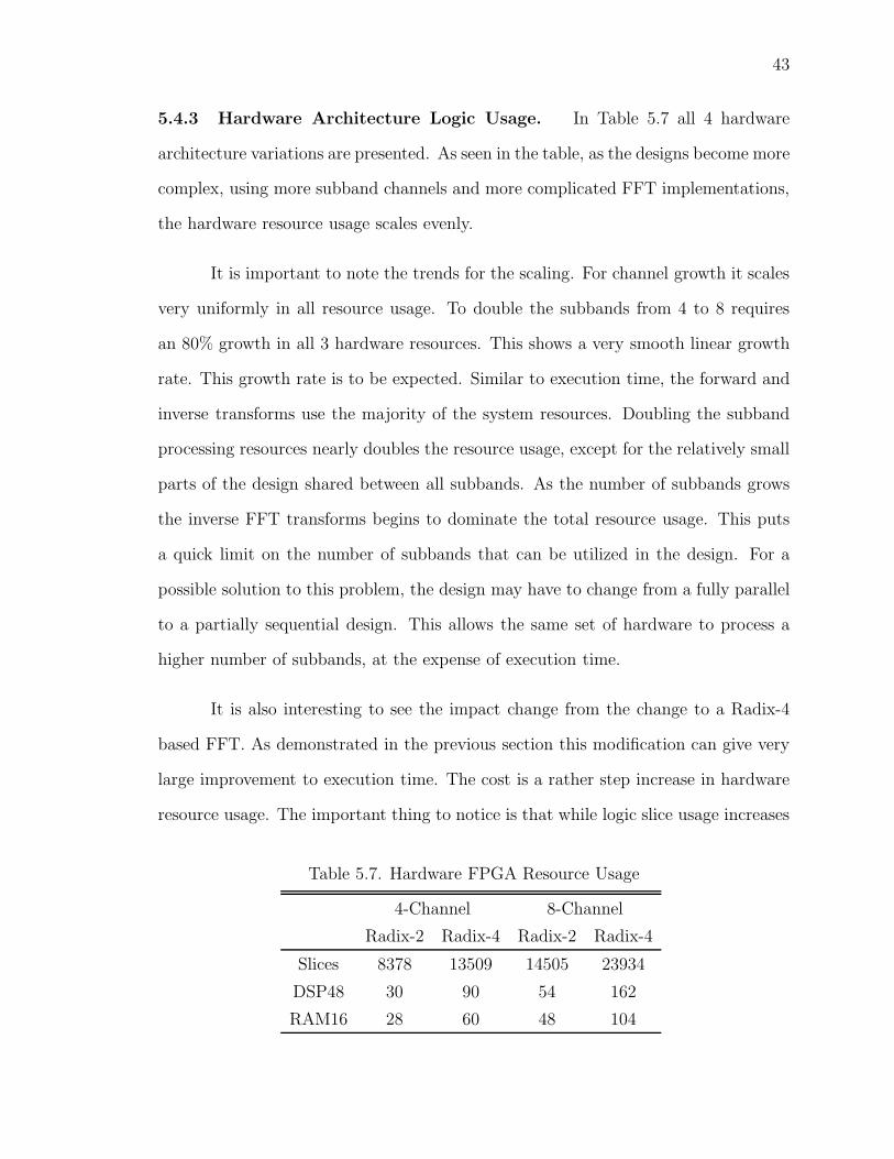
5.4.3 Hardware Architecture Logic Usage. In Table 5.7 all 4 hardware
architecture variations are presented. As seen in the table, as the designs become more
complex, using more subband channels and more complicated FFT implementations,
the hardware resource usage scales evenly.
It is important to note the trends for the scaling. For channel growth it scales
very uniformly in all resource usage. To double the subbands from 4 to 8 requires
an 80% growth in all 3 hardware resources. This shows a very smooth linear growth
rate. This growth rate is to be expected. Similar to execution time, the forward and
inverse transforms use the majority of the system resources. Doubling the subband
processing resources nearly doubles the resource usage, except for the relatively small
parts of the design shared between all subbands. As the number of subbands grows
the inverse FFT transforms begins to dominate the total resource usage. This puts
a quick limit on the number of subbands that can be utilized in the design. For a
possible solution to this problem, the design may have to change from a fully parallel
to a partially sequential design. This allows the same set of hardware to process a
higher number of subbands, at the expense of execution time.
It is also interesting to see the impact change from the change to a Radix-4
based FFT. As demonstrated in the previous section this modification can give very
large improvement to execution time. The cost is a rather step increase in hardware
resource usage. The important thing to notice is that while logic slice usage increases
Table 5.7. Hardware FPGA Resource Usage
4-Channel 8-Channel
Radix-2 Radix-4 Radix-2 Radix-4
Slices 8378 13509 14505 23934
DSP48 30 90 54 162
RAM16 28 60 48 104

44
at a reasonable 60% rate, memory usage doubled and DSP usage tripled. The Radix-4
implementation makes much heavier use of the built in mathematical DSP processing
blocks and begins to consume a significant large amount. This is important if the
design will be ported to other FPGA devices. If other FPGA may not have the same
amount of type of DSP execution units then the logical slice usage could drastically
increase when porting this design to alternate FPGA devices.
Of final importance is the overall resource consumption. For the Xilinx Virtex
4 device used (SX35) all of the designs are able to fit within the device, although the
Radix-4 8 channel implementation is starting to use the majority of the resources.
Changes to exceed 8 channels or to an even more complicated FFT implementation
would be difficult to implement on this FPGA device. In addition the largest of
these designs fail to provide adequate room for more complex implementations of the
alternate processing blocks. Different window filters, such as more complex Gaussian
filters may wish to be tried, or more advanced post processing, such as averaging or
neural networks will all need more logic resources to be implemented. In some cases
it may be preferential to allocate more resources to these modules, then to use them
to increase FFT performance or increase subbands.
5.5 Design Space Considerations
To see the true value of these results this research demonstrates the interactions
between performance metrics and allows insight into the design space as a whole.
This view of the design from a high level systems stand point is very valuable. It
allows a designer to make intelligent structural design decisions based on expected
performance, without having to design and construct all the systems for comparison.
This paper will review this high level approach by evaluating the interplay between
FCR performance, execution time, and hardware resource consumption.

45
To ease in display of data resource consumption has been combined into a
single metric value. For resource consumption it is important to see not only the
total resources used but also the percentage of the available resources consumed. For
this presentation the 3 hardware resources, logic slices, DSP48s, and block RAMs,
will be combined. A value will be obtained by determining the total percentage of
the total available resources which have been utilized by each design.
Two comparisons between performance metrics are shown in Figure 5.3 and
Figure 5.2. As a sample designer evaluation we will return to the original goals of
this research, achievement of a real time processing architecture. Execution time is a
critical requirement, needing to exceed 1 KHz of performance. From Figure 5.3 it is
easy to see that the pure software based designs fail to achieve the necessary rate and
all the pure hardware based designs exceed the needed rate. Since the pure software
design are unable to perform at real time they can be dismissed as potential design
solutions. It is also important to notice that for execution time it is important only
to exceed the necessary rate, increase in performance beyond that provides for little
improvement to overall system performance.
The key design parameter remaining is to balance the resource costs with over
all FCR performance. Through reviewing Figure 5.2 it is easy to gain a cost/performance
overview of the various designs. For this limited set of designs the best cost/performance
is achieved by the 8-Channel Radix-2 implementation. It is able to easily meet the real
time requirements, achieve nearly optimal results and consume a moderate amount
of resource.
The ability to explore the design space is a key advantage of the architectures
presented. The architectures can quickly provide insight into the impact design ar-
chitecture choices have on performance. This allows for a much lower design time
and a better understanding of the impact of design decisions.

46
Figure 5.2. FCR Performance vs. Resource Usage
Figure 5.3. Execution Time vs. Resource Usage
47
CHAPTER 6
CONCLUSION
6.1 Concluding Remarks
The object of this thesis is to produce architectures that are able to achieve
real time frequency diverse target detection for ultrasonic imaging. In order to achieve
reliable target detection clutter noise from microstructure sources must be drastically
lowered. It has been shown that the Split Spectrum Processing (SSP) algorithm is
able to make large improvements to the Flaw-to-Clutter ratio (FCR).
Utilizing the SSP algorithm leads to many implementation difficulties. The
algorithm has a very high computational complexity, necessitating a highly opti-
mized implementation. The algorithm’s performance is highly impacted by parameter
choices, specifically overall structure of the algorithm, number of channels, transform
type selection, ect., and window filter placement. To over come these difficulties
two architectures are presented which take advantage of the system-on-a-chip (SOC)
design methodology.
The SOC methodology is a highly integrated design approach. It allows for
very high performance designs by integration of all processing components onto a
single chip. Two architectures based on this principle are presented, a pure hardware
architecture and a pure software architecture. Both of these architectures are com-
plete system designs and focus on providing both a high degree of performance and
large amount of flexibility to faciliate design modification.
The pure hardware architecture integrates the whole design as system of dis-
crete interoperating hardware components implemented on a field programmable gate
array (FPGA). This design provides a high performance design that is easily exten-
sible through modification of individual hardware components. The pure software

48
architecture implements the algorithm in C code, which is then run on an embedded
soft core Microblaze processor implemented on a FPGA. This design allows for the ad-
dition of software optimization principles, while still operating on a similar hardware
unit, FPGA device, which facilitates performance comparisons between architectures.
Initial implementations of both architectures were created and tested. To
further demonstrate the flexibility of the architecture additional alternate implemen-
tations were created. This set of design implementations were then run through
experimental conditions to obtain performance results.
The set of results demonstrates the ability of these architectures to fulfill the
stated objectives of real time frequency diverse target detection. Furthermore they
reveal the many design issues that arise in the hardware implementation of the design.
The architectures function as research and design tools. They allow for direct insight
into the implementation to observe what impact parameter and system level design
choices have on the implementation results. This allows a designer to make informed
system level design choices based on the ability of the system as a whole to meet
performance requirements.
The architectures are value tools that provide for insight into implementation
of the SSP algorithm for frequency diverse ultrasonic target detection. In addition the
principles used to create these architectures can be applied to many other applications
requiring high signal processing capabilities in a portable device.
6.2 Future Work
The research presented here opens up many future avenues of research. The
first of which is a more in depth analysis of SSP algorithmic changes. It has been
shown that for many cases alternate transforms other then the FFT can achieve
increased performance results [Oru05]. In addition to over all performance, these

49
alternate transforms must be explored to see their impact on system implementation.
Beyond the transforms themselves is the selection of post processing tech-
niques. Promising research has been done on the results of alternate order statistical
methods and neural network techniques for post processing. Modification to the al-
gorithm based on this research will have large impacts on hardware implementation.
These impacts can be explored through the use of the architectures presented.
It has also been demonstrated that for different input data sets varied SSP
implementation achieve a peak performance. It would be advantageous to be able to
perform multiple implementations at the same time to allow for selection of the best
performing one in real time. To accomplish this goal a reconfigurable architecture
would be needed that could support multiple transform and SSP implementations.
An architecture that addresses this idea has been proposed but not realized as a
hardware implementation [Oru05].
Beyond the SSP algorithm itself there are many research topics of interest in
signal processing. Many of the techniques used in the creation of the architectures
presented can be applied to other signal processing applications.

50
BIBLIOGRAPHY
[APR96] U. Abeyratne, A. Petropulu, and J. Reid. On modeling the tissue responsefrom ultrasonic b-scan images. IEEE Transactions on Medical Imaging,15:479–490, 1996.
[LV90] L. Landini and L. Verazzani. Spectral characterization of tissues mi-crostructure by ultrasounds: A stochastic approach. IEEE Transactions onUltrasonics, Ferroelectrics and Frequency Control, 37(5):448–456, Septem-ber 1990.
[Nal05] Nallatech. Virtex-4 XtremeDSP Development Kit User Guide, 2005.
[NBSF82] V. Newhouse, N. Bilgutay, J. Saniie, and E. Furgason. Flaw-to-grain echoenhancement by split-spectrum processing. Ultrasonics, 20:59–68, March1982.
[NS95] D. Nagle and J. Saniie. Performance analysis of linearly combined orderstatistic cfar detectors. IEEE Transactions on Aerospace and ElectronicSystems, 31(2):522–533, April 1995.
[Oru05] Erdal Oruklu. High Speed Architecture Design and Performance Evalua-tion of Frequency-Diverse Orthogonal Transforms For Ultrasonic ImagaingApplications. PhD thesis, Illinois Institute of Technology, May 2005.
[RL04] C. Rowen and S. Leibson. Enginering the Complex SoC: Fast, FlexibleDesign with Configurable Processors. Professional Technical Reference.Prentice Hall, Upper Saddle River, NJ, 2004.
[San81] J. Saniie. Ultrasonic Signal Processing: System Identification and Param-eter Estimation of Reverberant and Inhomogeneous Targets. PhD thesis,Purdue University, 1981.
[SDB90] J. Saniie, K. Donohue, and N. Bilgutay. Order statistic filters as postde-tection processors. IEEE Transactions on Acoustics, Speech, and SignalProcessing, 38(10):1722–1732, October 1990.
[SN92] J. Saniie and D. Nagle. Analysis of order statistic cfar threshold estimatorsfor improved ultrasonic flaw detection. IEEE Transactions on Ultrasonics,Ferroelectrics and Frequency Control, 35(5):618–630, September Septem-ber 1992.
[SND91] J. Saniie, D. Nagle, and K. Donohue. Analysis of order statistic fil-ters applied to ultrasonic flaw detection using split spectrum processing.IEEE Transactions on Ferroelectrics and Frequency Control, 38(2):133–140, March 1991.
[SWB88] J. Saniie, T. Wang, and N. Bilgutay. Statistical evaluation of backscatteredultrasonic grain signals. Journal of the Acoustical Society of America,84(1):400–408, July 1988.
[Wol02] W. Wolf. Modern VLSI Design:System-on-a-Chip Design. Modern Semi-conductor Design Series. Prentice Hall, Upper Saddle River, NJ, 2002.
[Xil07a] Xilinx,Inc. ExtremeDSP for Virtex-4 FPGAs User Guide, October 2007.

51
[Xil07b] Xilinx,Inc. Fast Fourier Transform v5.0, October 2007.
[Xil08] Xilinx,Inc. Virtex-4 User Guide, April 2008.