confidential - sundance · confidential approvals date ... flash memory attached exclusively to...
TRANSCRIPT

Page 1
Unit / Module Name: Dual DSP PMC Module
Unit / Module Number: SMT417
Used On: PMC Carriers
Document Issue: See Revision History
Date: See Revision History
CONFIDENTIAL
Approvals Date
Managing Director
Software Manager
Design Engineer
Sundance Digital Signal Processing Inc, 4790 Caughlin Parkway #233, Reno, NV 89509-0907, USA.This document is the property of Sundance and may not be copied nor communicated to a third partywithout the written permission of Sundance. © Sundance Digital Signal Processing Inc. 2003

Page 2
Revision History
Changes Made Issue Initials
5/30/06 First Draft, from 407 0.0 FRH
06/09/06 Revised RSL, added SMA connector, removed SLB,updated JTAG description, added external powerconnector, compliance references.
0.1 BV
6/16/06 Merged QL JTAG into Xilinx chain for manufacturingtesting. Separated QL/DSP clocks. Identified RSLallocation for different Virtex devices.
0.2 FRH
6/22/06 Updated top-level block diagram. Clarified FPGA blockdiagram and switch operation. Updated Sec 2.4regarding XMC standard. Added several illustrativefigures.
0.3 BV
08/28/06 2.1: Fixed typo in block diagram (SDR SDRAM is used).
2.2.5.3, 2.7: Set 64MHz as QL5064 local bus speed.
2.3.1: Added indication of SMT417 actual width.
2.3.4: Changed side 2 max component height to 1.5mm,reflecting change in PCB thickness to 2.0mm.
2.4.3: Added design change for PCIe compatibility.
2.7: Added descriptions of RSLCLK and XMC REFCLK.
2.8: Moved section 3.3 description to this section.
3.3: Added pinout of JTAG header connector.
3.4.1: Added description of signals for PCIe on XMC.
6.1, 6.2: Updated layout from PCB design.
6.3: Added edge-view from mechanical design.
6.4: Added side 1 and side 2 mechanical diagrams.
7.2: Updated Table 9, power budget
7.3: Changed BOM section to Ordering Information
RFC.2 BV

Page 3
List of Abbreviations
Abbreviation ExplanationASIC Application Specific Integrated Circuit
BOM Bill Of Materials
CMC Common Mezzanine Card
Comport Communications Port
DSP Digital Signal Processor
FMS Trade name for a flat-ribbon cable family from JST Mfg. Inc.
FPDP Front Panel Data Port
FPGA Field Programmable Gate Array
NA Not Applicable
OTP One-Time Programmable
PC Personal Computer
PCB Printed Circuit Board
PCI Peripheral Component Interconnect
PMC PCI Mezzanine Card
PrPMC Processor PMC
RF Radio Frequency
RSL Rocket Serial Link
SDB Sundance Digital Bus
SDRAM Synchronous Dynamic Random Access Memory
SHB Sundance High-speed Bus
SLB Sundance LVDS Bus
SMA Trade name for a threaded RF co-axial connector family
SMT Sundance Multiprocessor Technology
TBD To Be Determined
TI Texas Instruments
XMC Switched Mezzanine Card

Page 4
Table of Contents1 Introduction.................................................................................................................. 7
1.1 Overview................................................................................................................ 7
1.2 Module Features.................................................................................................... 7
1.3 Related Documents................................................................................................ 7
2 Functional Description................................................................................................ 82.1 Module Overview ................................................................................................... 8
2.2 Hardware Features ................................................................................................ 8
2.2.1 TI 6416........................................................................................................... 8
2.2.2 PCI Bridge...................................................................................................... 8
2.2.3 Memory .......................................................................................................... 8
2.2.4 JTAG.............................................................................................................. 8
2.2.5 FPGA ............................................................................................................. 9
2.3 PMC Standard ..................................................................................................... 13
2.3.1 General ........................................................................................................ 13
2.3.2 Voltage keying.............................................................................................. 13
2.3.3 Connectors................................................................................................... 13
2.3.4 Component heights ...................................................................................... 13
2.3.5 Standoffs...................................................................................................... 14
2.3.6 Power Consumption..................................................................................... 14
2.3.7 Cooling......................................................................................................... 14
2.3.8 Grounding .................................................................................................... 14
2.3.9 Compliance .................................................................................................. 14
2.4 XMC Standard ..................................................................................................... 14
2.4.1 General ........................................................................................................ 14
2.4.2 ANSI/VITA 42.2 Serial RapidIO Protocol Layer Standard ............................. 15
2.4.3 ANSI/VITA 42.3 PCI Express Protocol Layer Standard ................................ 15
2.5 Power Supplies.................................................................................................... 15
2.6 Reset Hierarchy ................................................................................................... 16
2.7 Clock sources ...................................................................................................... 16
2.8 JTAG ................................................................................................................... 17
2.8.1 JTAG Operation ........................................................................................... 17
3 Description of Interfaces........................................................................................... 183.1 PCI....................................................................................................................... 18
3.2 SHB ..................................................................................................................... 21
3.3 JTAG header ....................................................................................................... 23
3.4 XMC..................................................................................................................... 24

Page 5
3.4.1 PCIe Support................................................................................................ 24
4 FMS............................................................................................................................. 255 Control Register Settings.......................................................................................... 25
5.1 Control Packet Structure ...................................................................................... 25
5.2 Reading and Writing Registers............................................................................. 25
5.3 Memory Map ........................................................................................................ 25
6 PCB Layout ................................................................................................................ 266.1 Top ...................................................................................................................... 26
6.2 Bottom ................................................................................................................. 26
6.3 Edge View............................................................................................................ 26
6.4 Mechanical Layout Diagrams............................................................................... 27
7 Design Notes.............................................................................................................. 287.1 FPGA Choice....................................................................................................... 28
7.2 Power Estimate.................................................................................................... 28
7.3 Power Requirements............................................................................................ 29
7.4 Ordering Information ............................................................................................ 29

Page 6
Table of FiguresFigure 1 - Block diagram of the SMT417. .............................................................................. 8
Figure 2 - Block diagram of SMT417 FPGA (standard firmware) ........................................... 9
Figure 3 - Single-size PMC card (from IEEE 1386-2001)..................................................... 13
Figure 4 - Single-size XMC card (from ANSI/VITA 42)......................................................... 15
Figure 5 - Module Top View – Artist’s Conceptualization ..................................................... 26
Figure 6 - Module Bottom View – Artist’s Conceptualization................................................ 26
Figure 7 - Module Side View................................................................................................ 28
Table of TablesTable 1 - PMC P11/P12 Interface........................................................................................ 19
Table 2 - PMC P13/P14 Interface........................................................................................ 20
Table 3 - SHB Interface....................................................................................................... 21
Table 4 - XMC P15 pinout ................................................................................................... 24
Table 5 - FMS connector pinout .......................................................................................... 25
Table 6 – RSL Allocation vs. Virtex size .............................................................................. 28
Table 7 - Power Budget Based on Supply ........................................................................... 29

Page 7
1 Introduction1.1 OverviewThis document describes the implementation of a PMC module with two fixed-point DSPs,one large FPGA, and other interfaces described below. The details of this specification willinclude hardware and programmable logic aspects.
1.2 Module FeaturesThe main features of the SMT417 are listed below:
§ Two TI 6416T DSPs with independent SDRAM
§ Xilinx Virtex II Pro (FF1152 package)
§ Provision for data processing in FPGA
§ One XMC connector with 8 RSL data links
§ Two FMS connectors
§ Standard single-size PMC module
§ 66MHz 64-bit PCI interface with over 500MB/s data rate
§ Standard Sundance software interface
Additional features meeting ANSI/VITA 32 (PrPMC) spec for tall modules:
§ Two SHB AND one RSL (7x bidirectional RocketIO) interface for easy interconnection toSundance products.
§ One (1x bidirectional RocketIO) to a Samtec GRF1-J connector for interfacing to XilinxRocketIO connectivity boards and other custom multi-gigabit serial interface hardware.
1.3 Related Documents
[1] PCI Mezzanine Card (PMC) Specification – IEEE 1386-2001.
http://standards.ieee.org/reading/ieee/std/busarch/1386-2001_and_1386.1-2001.pdf
[2] Sundance High-speed Bus (SHB) Specification – Sundance.
http://sundance.com/docs/SHB%20Technical%20Specification.pdf
[3] External Interface User Manual – Sundance.
http://sundance.com/docs/Firmware.pdf
[4] Rocket Serial Link (RSL) Specification – Sundance.
http://www.sundance.com/docs/Specification_RSL.pdf
[5] Processor PMC (PrPMC) Specification – VITA 32.
http://www.vita.com/specifications.html
[6] (FMS) Specification - Sundance
ftp://ftp2.sundance.com/Pub/documentation/pdf-files/comm-port.pdf
[7] Switched Mezzanine Card (XMC) Specification- VITA 42
http://www.vita.com/specifications.html

Page 8
2 Functional Description2.1 Module OverviewThe following figure details the block diagram of the SMT417.
16x2.5Gbps
SerialLinks
XilinxVirtex 2FPGA
XC2VP30/40/50
XilinxCoolRunner
CPLDXC2C256
QuickLogicQL5064
PCI Bridge
128MB SDRSDRAM
128MB SDRSDRAM
512MBFLASH
PCI HostP11P12P13
Local Bus
TITMS320C416T
1GHz
TITMS320C416T
1GHz
JTAG-IN
JTAG-OUT
FPGA JTAG
CONFIG + JTAGMcBSP (x3)
McBSP (x3)
RSL
SHB
SHB
FMS
FMS
PMC P14
XMC P15
GRF-1
x7
x1
x8
EMIFA64-bit/133MHz
EMIFA64-bit/133MHz
64-bit/64MHz
EMIFB8-bit
64-bit/66MHz
16-bit
2x400MB/sParallel
2x20MB/sParallel
64xUser I/O
HPI
Multi-Gigabit Serial
High-Speed Parallel
Figure 1 - Block diagram of the SMT417.
The SMT417 allows for parallel DSP computation on data acquired from PCI, SHB or RSLinterfaces while conforming to a single-sized PMC form factor.
2.2 Hardware Features2.2.1 TI 6416Two Texas Instruments 320C6416T DSPs, up to 1GHz, are present in this design. BothDSPs will have equal access to the PCI bus via logic within the Virtex FPGA. DSPA will beresponsible for initial configuration of DSPB, and will have the ability to configure the FPGA.
2.2.2 PCI BridgeThe PCI bridge is a separate hardware component. It is implemented as a QuickLogicQL5064 device which includes a hard PCI ASIC as well as an OTP fabric. The QL5064FPGA is preconfigured with the dedicated “Companion Design” logic from QuickLogic, whichprovides a very efficient multi-master 64-bit bus interface to the FPGA and allows the FPGAfull access to the DMA controllers, single-access PCI controller, and the target read/writebuffers. The QL5064 also has the ability to access the DSP JTAG chain. In cases where nohost is present, and therefore the state of the QL5064 is unknown, the rest of the board maycontinue to configure and run normally.
2.2.3 MemoryFlash memory attached exclusively to DSPA/EMIFB provides boot code and FPGAconfiguration data. Each DSP has separate banks of SDRAM for local processing on EMIFA.Up to 128MB of 64-bit SDRAM per DSP may be populated on the board, based on two512Mbit x32 parts per DSP (Total of 256MB on board).
2.2.4 JTAGA PCI-addressable CPLD provides JTAG access for Code Composer compatibility.Hardware is provided such that TI Code Composer can control the DSPs on the modulewithout need for additional cables.

Page 9
2.2.5 FPGAA standard Xilinx Parallel-IV JTAG interface is provided to allow the user to interface directlyto the FPGA.
Additionally, the PCI-addressable CPLD implements the SelectMAP interface to program theFPGA. This allows the FPGA on the SMT417 to be programmed by either DSPA or the PCIinterface. Software is provided such that a user can program the FPGA via the PCI buswithout need for additional cables.
2.2.5.1 FPGA block diagram
DSPAEMIFA
78
DSPBEMIFA
78
SHBA
60
15
CP3
CP0
SHBB
User-defined
Switch
Select
PCIBridge
64
1
21
DSP
AM
cBS
P 21
DSP
BM
cBS
P
RS
Lx7
P14
28FMS
SDB
SDB
SDB
SDB
PCIA
Comport
Comport
PCIB
FMS
Comport
Comport
XMC
(RS
Lx8
)
32CP0
CP3
4S
MA-
RF
(RS
Lx1
)4
6012
12
66
Figure 2 - Block diagram of SMT417 FPGA (standard firmware)
The basic architecture of the FPGA implements an EMIF target interface to each of theDSPs. Each DSP accesses its resources independently and concurrently of the other.Resources such as comports, SDBs, the PCI interface and the user-defined blocks arememory mapped into the DSPs EMIF. The DSP’s DMA engines and device drivers areresponsible for pushing or pulling data to and from the resources respectively.
The switch is statically configured by DSPA after reset, and remains set for the duration ofoperation (until the next reset). Standard Sundance device drivers on the DSP have thecapability of supporting up to 4 SDB ports and up to 6 Comport link ports mapped on theEMIF of any given DSP processor. Control of the switch is a memory mapped registerwhose value can be defined in flash and programmed by the boot loader.
User-defined resources can be mapped into the EMIF as appropriate and necessary for thecustomer application.

Page 10
2.2.5.2 ComportsComports will be implemented in order to allow communication between the DSPs. Whenrunning 3L Diamond software a Comport is required for loading applications. Each DSP willhave an independent set of Comport interfaces; Comport0 of DSPA will be bridged toComport3 of DSPB to allow standard Diamond software to function normally.
Each Comport includes a status register indicating the current port direction and number ofFIFO entries (for each direction). The Comport will be implemented with 32-word bi-directional FIFOs. Interrupts generated by the Comports will be routed through standardSundance interfaces.1
2.2.5.3 PCIA Comport-like interface will also be provided to interface each DSP to the PCI bridge. Thedifferences between this interface and a standard Comport is the 64-bit data path and theFIFO buffering depth. The 64-bit data path from each DSP EMIFA, through the FPGA, to thePCI bus allows for maximum performance using currently established softwareimplementations. The interface between the FPGA and PCI bridge is determined by thespeed grade of the QL5064 device that is ordered. This will be a minimum of 60MHz, andtypically 64MHz across all temperature ranges2.
2.2.5.4 SHBThe SMT417 can include two Sundance High-speed Bus (SHB) interfaces, both on side twoof the board. They are connected directly to the FPGA device, and can support data rates of3.2Gbps each (32-bit @100MHz). The SHBs can be configured for data widths of 8, 16, or32-bits. The SHB FIFO is 512 words deep, and bi-directional.
The SHB interface will generate interrupts to the DSP when a predefined number of wordsare available in the FIFO. SHB interrupts will be routed through standard Sundanceinterfaces.
The default configuration will be for each SHB to implement 2 SDBs. Either DSP may controleither SHB through software setting of the switch matrix.
Pin2
Integral Ground plane
Pin 1
Alignment PinBlade and Beam Design
0.5mm
Figure 3 - SHB Connector
1 http://www.sundance.com/docs/Firmware.pdf2 The QL5064 companion design achieves a maximum of 65MHz operation across 0°-70° using -75(fastest) speed grade parts.

Page 11
Note that if the SHB connectors are mounted (a build-time option), the module becomesgoverned by the ANSI/VITA 32 specification (PrPMC). This may preclude spacing the PMCcarrier boards in adjacent slots.
2.2.5.5 Interrupts and miscellaneous I/ORegisters grouped under this heading serve to provide two basic functions: interrupt routingand I/O interfaces. The interrupt control registers (ICR) allow interrupts from any Comport orSHB or PCI I/O interfaces to be mapped to any of the four external interrupts connected tothe DSP.
2.2.5.6 FMS2 FMS connectors are provided on side 1 of the board.
Figure 4 - FMS Connector Detail
These are connected to Comports inside the FPGA, and can be routed as described inFigure 2, above. These are provided to make simple integration with other Sundance carrierboards to create multiprocessor systems. 3
2.2.5.7 XMCOne XMC primary (P15) connector is also provided on side 1, implementing 8 Rocket-Serial-Link (RSL) interfaces.
Figure 5 - XMC Connector Detail
3 http://www.sundance.com/docs/SDL%20Technical%20Specification.pdf

Page 12
2.2.5.8 JTAGThe ANSI/VITA 42 specification governs how the JTAG signals are to be treated. The boardwill not attach any devices to the PMC or XMC JTAG pins, but will route TDI->TDO tomaintain integrity of any chains on the carrier boards. All manufacturing tests of the SMT417are performed using the dedicated JTAG header.
2.2.5.9 User-defined I/OEach DSP will provide the following additional interfaces to the FPGA:
q 3x McBSP
The following external interfaces will be provided for user-defined functions:
q PMC P14 (64-bits including 2 global clocks). This port will be made 5V tolerant throughthe use of “zero-delay” bidirectional FET switches. NOTE, these are the only 5V tolerantpins that interface directly to the FPGA. All other external interfaces must be clamped to4.5V.
2.2.5.10 RSLsThree Rocket Serial Link interfaces are present in this design.
1. A Sundance RSL connector with up to 7 bidirectional links routed to it. Note, that theRLS specification defines only 6 bidirectional pairs, but the connector allows for 14signal pairs, so the 7th link is connected.
2. The XMC connector implements 8 bidirectional links according to ANSI/VITA 42.2(Serial RapidIO for XMC)
3. A set of 4 coaxial connectors in a high-density mounting (5mm x 32.20mm) fromSamtec. The GRF1-J PCB connector mates with a GRF1-C cable end to provide ameans to expose a single 1x bidirectional RSL.
Figure 6 - Sundance RSL Connector Detail

Page 13
2.2.5.11 External PowerThe SMT417 derives is supply voltage from the PMC/XMC bus. Many customers desire touse the board in a stand-alone (non PMC/PCI) mode. For this purpose, a connector can beoptionally fitted to provide the +3.3V and +5V voltages from which the operating voltages arederived.
2.3 PMC Standard2.3.1 GeneralPMC is a variant of CMC that uses PCI to communicate over the backplane. The IEEE CMCstandard describes both single- and double-size mezzanine cards. The SMT417 will be asingle-size card.
Figure 7 - Single-size PMC card (from IEEE 1386-2001)
Dimensions of the single-size CMC are 74.0mm wide by 149.0mm deep. Note that theSMT417 does not provide any front panel connectors or ports, as per the ANSI/VITA 20(conduction cooled specification). Therefore, the SMT417 is 143.75mm deep.
2.3.2 Voltage keyingThe QuickLogic 5064 bridge is both 3.3V and 5V compliant. Both keying holes will beprovided. Note that the SMT417 requires both 3.3V and 5V power to function.
2.3.3 ConnectorsAccording to IEEE 1386.1-2001 connectors Pn1 through Pn3 are required for 64-bit PCIconnectivity. Additionally, connector Pn4 shall be provided for 64 bits of user-defined I/O.Given that the SMT417 is a single-size card, these connectors are referenced P11 throughP14.
2.3.4 Component heightsHeights of components on PMC Side 1 (see Figure 3) are limited to 4.7mm except in the I/OArea (where they may extend to the host module surface). Components on PMC Side 2 (seeFigure 3) are limited to 3.5mm minus PCB thickness, or about 1.5mm (assuming 2.0mm PCBthickness).
Given that neither the DSPs nor FPGA meet the clearance requirement, only the slightestparts such as memories and discrete components will be allowed on Side 2. Note that theSMT417 has build options which place certain connectors onto Side 2. When ordered in this
Page 14
way, the SMT417 conforms to ANSI/VITA 32 (PrPMC), which allows 10mm to 20mm ofheight above the PCB for components on Side 2.
2.3.5 StandoffsThere shall be two standoffs as part of the module. The standoffs should be of standard10mm height in order to support the broadest range of host modules.
2.3.6 Power ConsumptionDue to the close packing of components between PMC Side 1 and the host module, powerconsumption for convection (air) cooling is limited to 4.0W for 10.0mm standoffs (thisincreases to 6.0W for 13.0mm standoffs). The total consumption for Side 1 and Side 2 of themodule shall not exceed 7.5W.
The following information shall be provided on the PMC card:
q 5V current drawn, peak and average
q 3.3V current drawn, peak and average
Note: While it may appear that a stacking height of 13.0mm is desirable, some hosts may notaccept this.
Note: Depending on the operating frequency and user-defined FPGA designs implemented,the SMT417 is easily capable of exceeding the recommended power dissipation limits.Careful planning at both the software and firmware levels is required when integrating theSMT417 into end-user systems.2.3.7 Cooling
The SMT417 is designed to be used with conduction-cooled PMC carriers and systems. Thespecifications governing this are defined by ANSI/VITA 20-2001. The specification definescertain areas on the PMC board to be reserved free of components, to contain significantamounts of metal for thermal conductivity and to provide numerous through-hole terminalsfor attaching thermal and stiffening components.
2.3.8 GroundingPer section 4.14 of IEEE 1386-2001.
2.3.9 ComplianceThe SMT417 shall conform to EN61000-4-2 for EMC and ANSI/VITA 47-2005 for othermechanical and environmental requirements.
2.4 XMC Standard2.4.1 GeneralXMC is an extension of CMC that uses implements multi-gigabit switched serial connectionsto the backplane. The ANSI/VITA 42 standard describes both single- and double-sizemezzanine cards. The SMT417 will be a single-size card implementing an 8-lane interface tothe XMC connector.

Page 15
Figure 8 - Single-size XMC card (from ANSI/VITA 42)
2.4.2 ANSI/VITA 42.2 Serial RapidIO Protocol Layer StandardANSI/VITA 42.2 defines requirements and considerations for implementing Serial RapidIOover XMC to switched serial carriers. The SMT417 will be electrically compatible with thisstandard. Two x4 links will be available to the connector. A user will have the option ofintroducing a Serial RapidIO core to the FPGA on the SMT417 to allow it to interact with thefabric.
2.4.3 ANSI/VITA 42.3 PCI Express Protocol Layer StandardANSI/VITA 42.3 defines requirements and considerations for implementing PCI Express overXMC to switched serial carriers. The SMT417 will be4 electrically compatible with thisstandard. One x8 link will be available to the connector. A user will have the option ofintroducing a PCI Express core to the FPGA on the SMT417 to allow it to interact with thefabric.
2.5 Power SuppliesThe SMT417 shall conform to the PMC standard for single-size modules. The PCIconnectors supply the module with 5.0V and 3.3V power supply. The 3.3V will be used tosupply all LVTTL digital I/O voltages directly, including the FPGA I/O rail VCCO. The FPGACore Voltage (VCCINT = 1.5V, up to 10A) and DSP Core Voltage (VDSP = 1.2V, up to 5A) aregenerated from the 5.0V by high-efficiency DC/DC converters. To avoid problems with theFPGA, the ramp rate of VCCINT is limited by soft-start circuitry to between 200us and 50ms.
The FPGA Auxiliary voltage (VCCAUX = 2.5V) is derived from 3.3V using a linear LDOregulator to minimise losses.
2.5V Power for the Rocket-IO sections of the FPGA is supplied by two independent linearregulators,
Note: On 11/17/04, the Virtex-IIPro datasheet was amended, removing the requirement forspecial power-supply sequencing. From the v4.5 datasheet: VCCAUX and VCCO canpower on at any ramp rate. Power supplies can be turned on in any sequence.
4 The PCIe reference clock (REFCLK+/-) needs to be handled by a PLL:
http://www.xilinx.com/xlnx/xil_ans_display.jsp?BV_UseBVCookie=yes&getPagePath=18329
The SMT417 design uses a single ICS874005 to perform the 100MHz -> 125MHz conversion:
http://www.icst.com/icscs/SiteSearch.aspx?q=ICS874005

Page 16
2.6 Reset HierarchyThe SMT417 shall obey the reset signal provided by the PCI connector; however this signalwill only reset the QL5064. If desired, the DSPs and FPGA may be reset via PCI controlthrough the CPLD interface. Additionally, the DSPs may also reset the FPGA. In any casethe FPGA reset should not be released until the FPGA configuration has completed. Properoperation of the board in a stand-alone configuration (no PCI host present, no PCI clock) willbe insured by use of a dedicated reset generator.
There are two fundamental scenarios at power-on:
1. PCI-controlled: The PCI bus resets the QL5064. Following PCI enumeration thedriver software asserts reset to the DSPs and FPGA, configures the FPGA, loadscode into DSPA and/or DSPB via JTAG, and releases the resets. Note that in thiscase, if there is valid code in the flash memory, the DSPs may start to execute codebefore the host PC has gotten around to asserting reset. This is a necessaryconsequence of supporting the following non-PCI case, where the state of theQL5064 is undefined. If this could be a problem, a “NOP” program should be loadedinto the flash memory.
2. “Embedded The PCI bus may or may not be connected. Following the expiration ofthe on-board reset timer, DSPA begins to execute code from the flash memory. Thiscode likely contains a configuration for the FPGA which will be loaded by DSPA, aswell as code to be loaded into DSPB through that processor’s host port. DSPB willnot begin execution until commanded to do so by host-port control. Once the FPGAand DSPB have been configured, the two DSPs may communicate with each otherthrough the FPGA, and other peripherals through various comports.
2.7 Clock sourcesThere are several independent clock sources on the SMT417:
1. PCI Clock: From the external PCI host, this clock is connected only to the QL5064.This clock may be idle if no external host is present.
2. QLCLK: The clock for the FPGA side of the QL5064, a dedicated crystal oscillatorprovides 64MHz. This clock is distributed to the QL5064, the Virtex FPGA and thecontrol CPLD.
3. DSPCLKA/B: Both DSPs have a fixed 50MHz clock input, and may be configured torun at in internal clock rate which is any supported multiple of this frequency. For a1G device this includes 1GHz (x20), 600MHz (x12), and 300MHz (x6); for all otherspeed grades the internal DSP clock may be 600MHz or 300MHz. The crystaloscillator may be populated with a different value to support other DSP clock speeds.
4. EMIFCLK: Both DSPs are supplied with a single clock to use with the two EMIFports. If the DSP is operating at no more than 800MHz, the user has the option ofgenerating the EMIF clock by dividing-down the DSP clock by 6, or by using theexternal clock. Whichever clock is chosen by software will be passed to the externaldevices through the ECLKOUT pins. EMIFA and EMIFB may be configuredseparately. If the DSP clock is faster than 800MHz, then the external EMIF clockmust be selected for both EMIFA and EMIFB. The frequency of the EMIF crystal maybe selected at build time based on the speed of the SDRAM devices installed,(133MHz default). The EMIFB clock input runs at ½ the rate of the EMIFA clockinput.
5. RSLCLK: An LVPECL (differential) clock source is required to generate the 2.5GHz –3.125GHz MGT clocks. A dedicated crystal oscillator provides 125MHz.

Page 17
6. XMC REFCLK: When the SMT417 is used in a PCIe environment, the referenceclock must be used to generate the 2.5GHz MGT clock. The XMC REFCLK is100MHz, which must be translated to 125MHz for the FPGA to generate 2.5GHz.This is accomplished by an ICS874005 LVPECL jitter cleaner and PLL device.
2.8 JTAGThere are two distinct JTAG chains present on the SMT417:
1. The Xilinx JTAG chain is used to access the XC2VP FPGA + CoolRunnerII CPLD.The chain is brought out to a high-density debug header, and is used to update theCPLD firmware and to assist in board bring-up and debug of the FPGA firmware.The QL5064 JTAG interface is also on this chain, and is used for manufacturing testonly. When programming the FPGA using an external JTAG controller, it is importantto configure the tool to bypass both the CPLD and the QL5064.
2. The TI DSP JTAG chain connects the two DSPs to separate pins on the same high-density debug header. Additionally, this chain terminates into I/O pins of theCoolRunnerII CPLD. The CPLD can function as a Master (driver) of the chain, or asa Linker (transparent) according the debug mode desired. When functioning as amaster, the CPLD is under the control of the host driver. This chain is used to controland debug DSP software, as well as to run the Sundance FLASH programming utilitywhen managing the contents of the FLASH.
The XMC and PMC connectors also provide JTAG pins, but they are not used on theSMT417 and are simply tied TDI->TDO to maintain integrity of any chains that may beimplemented on the carrier cards.
The SMT417 attempts to maximize compatibility with existing practices and software. TheXilinx and TI JTAG chains are kept separate, allowing both sets of devices to be connectedto corresponding standard external controllers as needed.
Both JTAG-IN and JTAG-OUT for the DSP JTAG are provided to allow daisy-chaining ofmultiple DSP boards. Alternatively, users may target Code Composer Studio to the DSPboards directly through the PCI interface without connecting an external emulator.
Due to board real estate constraints, it was not possible to use standard headers for theexternal JTAG. The SMT417 implements a proprietary high-density debug header to allowthe Xilinx and DSP JTAG headers to be available. A small companion PCB and short cableinterfaces to this high-density connector and provides standard Xilinx Parallel Cable IV orPlatform Cable USB and TI XDS510 (IN and OUT) emulation headers.
2.8.1 JTAG OperationThe default state of the CPLD is to provide (transparent) operation to the DSP JTAG chainsfrom the external connector. Through the programming of control registers accessible fromthe PCI host, the CPLD is capable of driving the DSP JTAG chain as a scan path controller.During stand-alone operation, the PCI is inactive, so the CPLD operates in its default state.

Page 18
3 Description of Interfaces3.1 PCIA 66MHz 64-bit PCI bridge allows the SMT417 to communicate with the host module. Giventhis bus architecture, transfer rates of over 500MB/s may be achievable. This interface isalso completely backward-compatible with 32bit and/or 32MHz PCI hosts.
The minimum addressable functions include a high-speed Comport-like interface to eachDSP, as well as any user-defined interfaces that may be built inside the Virtex FPGA. Accessis also provided to a JTAG master attached to both DSPs on one chain, through a CPLD thatalso arbitrates configuration of the FPGA via the FPGA’s SelectMAP port.
PMC PCI connectors are directly connected to the QuickLogic QL5064 bridge chip.
P11 P12
Pin # Signal name Signal name Pin # Pin # Signal name Signal name Pin #
1 TCK -12V 2 1 +12V TRSTN 2
3 GND INTAN 4 3 TMS TDO 4
5 INTBN INTCN 6 5 TDI GND 6
7 BUSMODE1N +5V 8 7 GND PCI-RSVD* 8
9 INTDN PCI-RSVD* 10 9 PCI-RSVD* PCI-RSVD* 10
11 GND 3.3Vaux 12 11 BUSMODE2N +3.3V 12
13 CLK GND 14 13 RSTN BUSMODE3N 14
15 GND GNTN 16 15 +3.3V BUSMODE4N 16
17 REQN +5V 18 17 PMEN GND 18
19 VIO AD31 20 19 AD30 AD29 20
21 AD28 AD27 22 21 GND AD26 22
23 AD25 GND 24 23 AD24 +3.3V 24
25 GND C/BE3N 26 25 IDSEL AD23 26
27 AD22 AD21 28 27 +3.3V AD20 28
29 AD19 +5V 30 29 AD18 GND 30
31 VIO AD17 32 31 AD16 C/BE2N 32
33 FRAMEN GND 34 33 GND PMC-RSVD 34
35 GND IRDYN 36 35 TRDYN +3.3V 36
37 DEVSELN +5V 38 37 GND STOPN 38
39 GND LOCKN 40 39 PERRN GND 40
41 PCI-RSVD* PCI-RSVD* 42 41 +3.3V SERRN 42
43 PAR GND 44 43 C/BE1N GND 44
45 VIO AD15 46 45 AD14 AD13 46
47 AD12 AD11 48 47 M66EN AD10 48

Page 19
49 AD9 +5V 50 49 AD8 +3.3V 50
51 GND C/BE0N 52 51 AD7 PMC-RSVD 52
53 AD6 AD5 54 53 +3.3V PMC-RSVD 54
55 AD4 GND 56 55 PMC-RSVD GND 56
57 VIO AD3 58 57 PMC-RSVD PMC-RSVD 58
59 AD2 AD1 60 59 GND PMC-RSVD 60
61 AD0 +5V 62 61 ACK64N +3.3V 62
63 GND REQ64N 64 63 GND PMC-RSVD 64
Table 1 - PMC P11/P12 Interface
P13 P14
Pin # Signal name Signal name Pin # Pin # Signal name Signal name Pin #
1 PCI-RSVD GND 2 1 I/O I/O 2
3 GND C/BE7N 4 3 I/O I/O 4
5 C/BE6N C/BE5N 6 5 I/O I/O 6
7 C/BE4N GND 8 7 I/O I/O 8
9 VIO PAR64 10 9 I/O I/O 10
11 AD63 AD62 12 11 I/O I/O 12
13 AD61 GND 14 13 I/O I/O 14
15 GND AD60 16 15 I/O I/O 16
17 AD59 AD58 18 17 I/O I/O 18
19 AD57 GND 20 19 I/O I/O 20
21 VIO AD56 22 21 I/O I/O 22
23 AD55 AD54 24 23 I/O I/O 24
25 AD53 GND 26 25 I/O I/O 26
27 GND AD52 28 27 I/O I/O 28
29 AD51 AD50 30 29 I/O I/O 30
31 AD49 GND 32 31 I/O I/O 32
33 GND AD48 34 33 I/O I/O 34
35 AD47 AD46 36 35 I/O I/O 36
37 AD45 GND 38 37 I/O I/O 38
39 VIO AD44 40 39 I/O I/O 40
41 AD43 AD42 42 41 I/O I/O 42
43 AD41 GND 44 43 I/O I/O 44
45 GND AD40 46 45 I/O I/O 46

Page 20
47 AD39 AD38 48 47 I/O I/O 48
49 AD37 GND 50 49 I/O I/O 50
51 GND AD36 52 51 I/O I/O 52
53 AD35 AD34 54 53 I/O I/O 54
55 AD33 GND 56 55 I/O I/O 56
57 VIO AD32 58 57 I/O I/O 58
59 PCI-RSVD PCI-RSVD 60 59 I/O I/O 60
61 PCI-RSVD GND 62 61 I/O I/O 62
63 GND PCI-RSVD 64 62 I/O I/O 64
Table 2 - PMC P13/P14 Interface

Page 21
3.2 SHBThe SMT417 has two SHB connectors, both on side 2:
Hw QSH Pinnumber
QSH Pinnumber
Hw
SHBxCLK0 1 2 SHBxD0(0)
SHBxD0(1) 3 4 SHBxD0(2)
SHBxD0(3) 5 6 SHBxD0(4)
SHBxD0(5) 7 8 SHBxD0(6)
SHBxD0(7) 9 10 SHBxD0(8)
SHBxD0(9) 11 12 SHBxD0(10)
SHBxD0(11) 13 14 SHBxD0(12)
SHBxD0(13) 15 16 SHBxD0(14)
SHBxD0(15) 17 18 SHBxUSER0(16)
SHBxUSER0(17) 19 20 SHBxUSER0(18)
SHBxUSER0(19) 21 22 SHBxWEN1
Hw
0
SHBxREQ1 23 24 Hw
0
SHBxACK1
SHBxUSER1(23) 25 26 SHBxUSER1(24)
SHBxUSER1(25) 27 28 SHBxUSER1(26)
SHBxUSER1(27) 29 30 SHBxUSER1(28)
SHBxUSER1(29) 31 32 SHBxUSER1(30)
SHBxUSER1(31) 33 34 SHBxUSER1(32)
SHBxUSER1(33) 35 36 SHBxUSER1(34)
SHBxCLK3 37 38 SHBxD1(0)
SHBxD1(1) 39 40 SHBxD1(2)
SHBxD1(3) 41 42 SHBxD1(4)
SHBxD1(5) 43 44 SHBxD1(6)
SHBxD1(7) 45 46 SHBxD1(8)
SHBxD1(9) 47 48 SHBxD1(10)
SHBxD1(11) 49 50 SHBxD1(12)
SHBxD1(13) 51 52 SHBxD1(14)
SHBxD1(15) 53 54 SHBxUSER2(52)
SHBxUSER2(53) 55 56 SHBxUSER2(54)
SHBxUSER2(55) 57 58 SHBxWEN4
Hw
1
SHBxREQ4 59 60 Hw
1
SHBxACK4
Table 3 - SHB Interface

Page 22
The SHB signals have been named to match 2 16-bit SDB interfaces (or Hw SHB interface)pinout according to the SUNDANCE SHB specification Half Word configuration.
Typically right-angle SHB cables are used:
http://www.sundance.com/edge/files/productpage.asp?strfilter=smt512-120

Page 23
3.3 JTAG headerDue to board real estate constraints, it was not possible to use standard headers for theexternal JTAG chains. The SMT417 implements a proprietary high-density debug header toallow the Xilinx and DSP JTAG headers to be available. The header is an FTS-110-02-F-DVfor an IDC ribbon cable. A small companion PCB and short cable interfaces to this high-density connector and provides standard Xilinx Parallel Cable IV or Platform Cable USB andTI XDS510 (IN and OUT) emulation headers.
Signal Pin No. Function TypeDEMU0 17 DSP EMU0 I/ODEMU1 19 DSP EMU1 I/O
DNTRST 5 DSP /TRST InDPDN5
18 DSP /PD Out
DTCK 11 DSP TCK InDTCK_RET 15 DSP TCK_RET OutDTDI 1 DSP TDI InDTDOB 13 DSP TDO OutDTMS 3 DSP TMS I/O
FTCK 8 FPGA TCK InFTDI6 14 FPGA TDI InFTDO7
12 FPGA TDO Out
FTMS 6 FPGA TMS I/OGND 7,9,10,16,20 GroundV33 2,4 +3.3V
Table 4 JTAG header pinout
5 DPDN= nDJPRESENT on schematic6 FTDI=CTDI on schematic7 FTDO=QTDO on schematic
Page 24
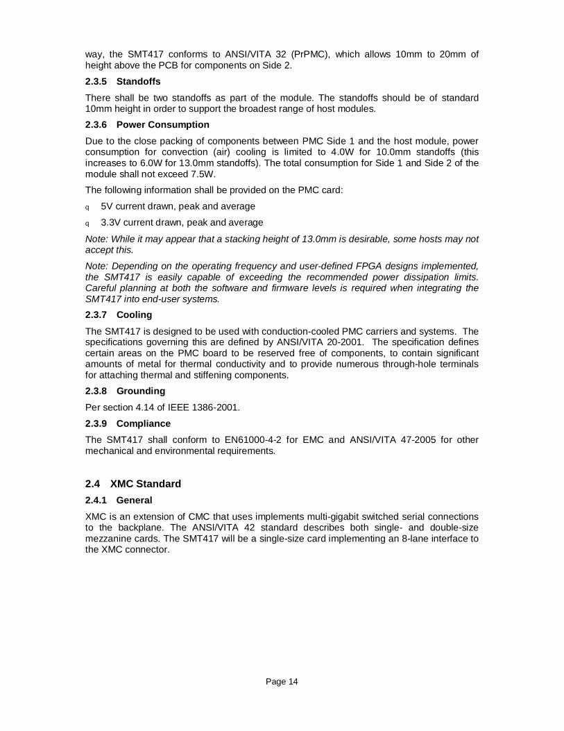
3.4 XMCThe XMC connector conforms to the type, position, and pinout specified in VITA 42.2 forXMC serial RapidIO. The pinout is shown below.
Table 5 - XMC P15 pinout
3.4.1 PCIe SupportIn order to support PCIe operation over the XMC connector, the following signals areimplemented according to ANSI/VITA 42.3:
A B C D E F19 REFCLK+0 REFCLK-0 WAKE# ROOT0#
Table 6 - XMC P15 pins for PCIe

Page 25
4 FMSTwo FMS connectors are provided on side 1, and conform to the Sundance “Comm-ports”spec to implement one comm. port each. The connectors are single-row 14-pin type with0.6mm pitch, and the pinout follows in table 7. To determine ownership of the port oninitialization, one of the two “detect” pins may be pulled-up to 3.3V while the other isgrounded by the FPGA. If each side sees that both pins have been forced to ground then itmay be understood that one port has initially been configured as an input and the other as anoutput. On the SMT417 this may be configured through the FPGA.
Signal Pin No. Function TypeDET1 1 Direction-indicator I/OCxD(0-7) 2-9 Comm-Port DataBus I/O
CREQx 10 Comm-Port Token Request I/O
CACKx 11 Comm-Port Token Acknowledge I/O
CSTRBx 12 Comm-Port Data Strobe I/O
CRDYx 13 Comm-Port Ready I/ODET2 14 Direction-indicator I/O
Table 7 - FMS connector pinout
5 Control Register Settings5.1 Control Packet StructureNo special commands are defined.
5.2 Reading and Writing RegistersRegister formats and offsets for Comport, SDB/SHB, interrupt selection, etc. conform toSundance standard firmware specification8.
5.3 Memory MapMemory locations of standard Sundance functions conform to the Sundance standardfirmware specification. The FPGA base address is TBD.
8 http://www.sundance.com/docs/Firmware.pdf

Page 26
6 PCB Layout6.1 Top
Figure 9 - SMT417 v0.3 PCB Top Layout (Side 1)
6.2 Bottom
Figure 10 - SMT417 v0.3 PCB Bottom Layout (Side 2 X-RAY VIEW)
6.3 Edge View
Page 27
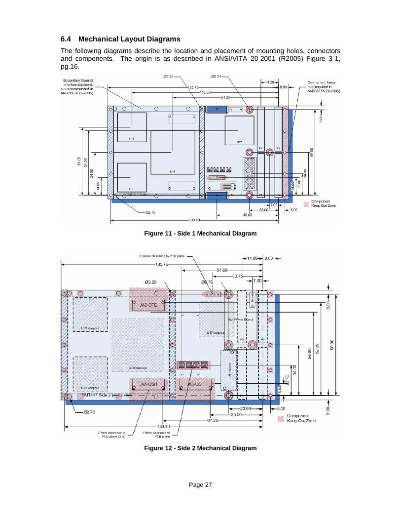
6.4 Mechanical Layout DiagramsThe following diagrams describe the location and placement of mounting holes, connectorsand components. The origin is as described in ANSI/VITA 20-2001 (R2005) Figure 3-1,pg.16.
Figure 11 - Side 1 Mechanical Diagram
Figure 12 - Side 2 Mechanical Diagram

Page 28
7 Design Notes7.1 FPGA ChoiceThe FPGA device will be a Xilinx Virtex II Pro of package type FF1152. In order to supportthe 637 total I/Os required by this design, the minimum device size will be a VP30. A VP50is the minimum size that supports all 16 RSL links possible on this board. Table 8 shows thenumber and allocation of RSLs for different Virtex devices.
Virtex Device XMC RSLs RSL Connector GRF-1
VP30 4 3 1
VP40 4 7 1
VP50 8 7 1
Table 8 – RSL Allocation vs. Virtex size
7.2 Power EstimateA power consumption estimate is performed for the following conditions:
• DSP CPU utilization of 60%, EMIF @133MHz, 50%, 70°C junction
• FPGA with standard firmware, PCI and SHB at 100% utilization
• Both DSPs active, no RSLs in use
Figure 13 - Full Power Estimation
Page 29
DSP power estimates are obtained from ‘spraa45.xls. FPGA power estimation is obtainedfrom web-based Xilinx Power Central. Other estimates are obtained from respectivemanufacturer datasheets.
The expected “full-power’ dissipation is 11.27W at 70C junction temperatures, not countingRSL consumption.
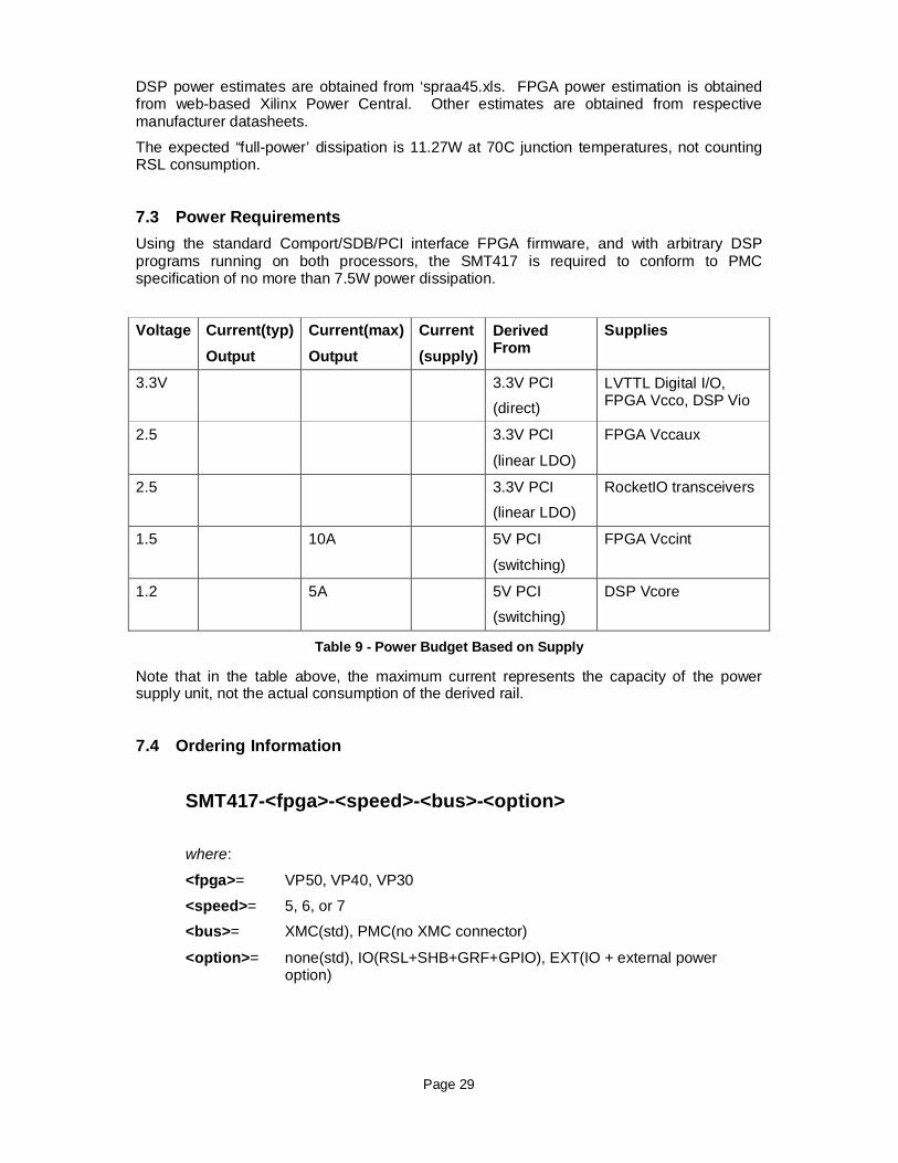
7.3 Power RequirementsUsing the standard Comport/SDB/PCI interface FPGA firmware, and with arbitrary DSPprograms running on both processors, the SMT417 is required to conform to PMCspecification of no more than 7.5W power dissipation.
Voltage Current(typ)Output
Current(max)Output
Current(supply)
DerivedFrom
Supplies
3.3V 3.3V PCI
(direct)LVTTL Digital I/O,FPGA Vcco, DSP Vio
2.5 3.3V PCI
(linear LDO)
FPGA Vccaux
2.5 3.3V PCI
(linear LDO)
RocketIO transceivers
1.5 10A 5V PCI
(switching)
FPGA Vccint
1.2 5A 5V PCI
(switching)
DSP Vcore
Table 9 - Power Budget Based on Supply
Note that in the table above, the maximum current represents the capacity of the powersupply unit, not the actual consumption of the derived rail.
7.4 Ordering Information
SMT417-<fpga>-<speed>-<bus>-<option>
where:
<fpga>= VP50, VP40, VP30
<speed>= 5, 6, or 7
<bus>= XMC(std), PMC(no XMC connector)
<option>= none(std), IO(RSL+SHB+GRF+GPIO), EXT(IO + external poweroption)