con - ohio state university
TRANSCRIPT

An Introduction to
The Design and Testing of Microwave Amplifiers
LABORATORY MANUAL
for the
EE 723 Adjunct Microwave Laboratory
Patrick Roblin
Associate Professor
The Ohio State University
2003 (12th Edition)

Contents
Acknowledgements 4
1 INTRODUCTION 5
1.1 Laboratory Overview . . . . . . . . . . . . . . . . . . . . . . . . . . . . . . . 5
1.2 The Laboratory Facilities . . . . . . . . . . . . . . . . . . . . . . . . . . . . . 5
1.3 Laboratory Policies . . . . . . . . . . . . . . . . . . . . . . . . . . . . . . . . 6
1.4 Laboratory Schedule and Report . . . . . . . . . . . . . . . . . . . . . . . . 6
2 LABORATORY 1:
Microwave Measurement of a Microwave Amplier 8
2.1 Preparation for Lab 1 . . . . . . . . . . . . . . . . . . . . . . . . . . . . . . . 8
2.2 PART I: Frequency and Gain Compression Measurement . . . . . . . . . . . 8
2.3 PART II: Measurement of the Noise Figure . . . . . . . . . . . . . . . . . . . 12
3 LABORATORY 2:
Measurement of the Scattering Parameters of a Microwave Transistor 16
4 LABORATORY 3:
Design of a Microwave Amplier 18
4.1 Design . . . . . . . . . . . . . . . . . . . . . . . . . . . . . . . . . . . . . . . 18
4.1.1 Important Design Constrains: . . . . . . . . . . . . . . . . . . . . . . 18
4.1.2 Design Procedure: . . . . . . . . . . . . . . . . . . . . . . . . . . . . . 18
4.1.3 Summary of the Design rules associated with the Fabrication . . . . . 21
4.2 Fabrication Procedure . . . . . . . . . . . . . . . . . . . . . . . . . . . . . . 23
4.3 Measurement of Your Circuit. . . . . . . . . . . . . . . . . . . . . . . . . . . 24
4.4 Write Up . . . . . . . . . . . . . . . . . . . . . . . . . . . . . . . . . . . . . . 25
4.4.1 The Laboratory Report . . . . . . . . . . . . . . . . . . . . . . . . . . 25
4.4.2 Poster Page . . . . . . . . . . . . . . . . . . . . . . . . . . . . . . . . 25
2

5 APPENDICES 27
5.1 How to Use ADS . . . . . . . . . . . . . . . . . . . . . . . . . . . . . . . . . 27
5.2 How to Use the Layout Tool . . . . . . . . . . . . . . . . . . . . . . . . . . . 28
5.3 How to Use LineCalc . . . . . . . . . . . . . . . . . . . . . . . . . . . . . . . 30
5.4 Tips for Soldering . . . . . . . . . . . . . . . . . . . . . . . . . . . . . . . . . 31
5.5 Caring About Connectors . . . . . . . . . . . . . . . . . . . . . . . . . . . . 33
5.6 AT42085 S-Parameters and Noise Parameters . . . . . . . . . . . . . . . . . 34
5.7 Computer Data Acquisition for 2-Port S-parameters . . . . . . . . . . . . . . 35
5.8 Loading S-parameter data in ADS and MATLAB . . . . . . . . . . . . . . . 37
5.9 Active Biasing Circuit . . . . . . . . . . . . . . . . . . . . . . . . . . . . . . 41
5.10 Laboratory Report Forms . . . . . . . . . . . . . . . . . . . . . . . . . . . . 43
3

Acknowledgements
This laboratory would not have been possible without the help and support of many
people whose contributions I would like to acknowledge.
Most of all I am very grateful to the Hewlett Packard/Agilent Technologies Company
for donating our rst Network Analyzer (now retired), the Spectrum Analyzer HP8592A and
Noise Figure meter HP8970B. Particular I would like to thank our famous OSU alumini Dr.
John Moll of HP Laboratories as well as Howard Boyd, Tom Nebel, and Je Skokal of the
local HP sale oce for their active support.
The Network Analyzer HP8753C currently used in the lab was acquired thanks to a
National Science Foundation education equipment grant.
Several parts and supplies have been generously donated by the microwave industry.
I would like to thank the Rogers Corporation for the donation of microstrip circuit boards;
and Agilent/Avantek for the donation of microwave transistors.
The rst demonstration microwave amplier was developed for this laboratory by
Truong X. Nguyen during the course of independent study projects.
I am most grateful to my graduate students Sung Choon Kang, Chih Ju Hung, Vakur
Erturk and Siraj Akhtar for their dedicated contribution to the development of this labora-
tory since 1992.
Finally I would like to thank Professors. H.C. Ko, B. Mayan, D. Hodge, and Y. Zheng
for the full support provided to this project as chairman of the EE department. Prof. Klein
on-going support is also acknowledged.
Patrick Roblin
January 2003
4

1. INTRODUCTION
1.1 Laboratory Overview
The EE 723 adjunct microwave laboratory is designed to run in parallel with EE 723. An
introduction to microwave amplier and oscillator design is given in the EE 723 lecture. In
support to the theory, the simulation and optimization of the microwave ampliers studied
are performed using an advanced microwave circuit simulator (ADS) in our ER4 computer
facilities. To complete the learning cycle the EE 723 adjunct microwave laboratory provides
the EE 723 students with the opportunity to experimentally verify the device principles and
design theory of the microwave devices and circuits studied. The two main objectives of the
laboratory are therefore:
1. To introduce the EE 723 student to the techniques and principles of microwave mea-
surement with a modern Network Analyzer.
2. To involve the EE 723 student in the design of an amplier. The project includes
rst principle design, CAD simulation and optimization, CAD layout, fabrication of a
prototype, and testing.
Note that the students who are interested in pursuing a design project of their own will have
the opportunity to do so under a follow-up independent study. Successful design projects
will be used as demo in the microwave laboratory.
1.2 The Laboratory Facilities
The measurement and fabrication facilities of the Education Microwave Laboratory are lo-
cated in CL 305
The measurement station consists of one HP 8753C Network Analyzer, the HP 8970B Noise
Figure meter, the HP437B Power meter, the HP 8592A Spectrum Analyzer, the Colorpro
HP Plotter, printer, the HP 6237B power supplies, and the HP 3457A multimeter.
A bench rack is available for storing your circuits under development. Please use the white
stickers available in CL 305 to write your name(s) on your circuits.
The circuits designed by the students are fabricated in CL305 using computer aided ma-
chining by the EE 723 teaching assistant. CL305 features a workbench, a tool box, various
drills, two dierent soldering irons, and a parts cabinet.
5
1.3 Laboratory Policies
For a proper and ecient sharing of the laboratory equipment a set of rules is necessary. The
latter make up the Laboratory policy. A sample of the Laboratory Policy is given below.
You are asked to read it and obide by its rules to participate in this laboratory.
EE 723 Laboratory Policy
1. Schedule your measurement and fabrication time (CL 305) in advance on the sign up
sheet on the door of CL 305. You can reserve up to 2 hours/per week. Open time is
however available on a rst come, rst served basis.
2. Read your laboratory manual and make a plan of work before coming to the lab.
3. You can obtain the laboratory key against your I.D card at the reception desk of the
EE department oce. The receptionist should check that you are on the EE 723 class
roster; remind him to do so!.
4. Make sure that the laboratory door is closed when you leave the room even for a short
period.
5. Care for the measurement cables and connectors (refer to Appendix 5.5 of your labo-
ratory manual) and the equipment in general. The measurements will be made using
SMA test cables. Do not disconnect the SMA test cables from the Network Analyzer.
Dirty cables lead to bad data.
6. Read soldering, drilling and cutting tips in the Appendices D, E and F of your labo-
ratory manual to ensure a proper use of the tools and to assure your proctection. If
you are uncomfortable with a particular laboratory procedure request help from the
instructor.
7. Report damage or malfunction immediately (you will not be penalized) to the instruc-
tor or teaching assistant.
1.4 Laboratory Schedule and Report
A laboratory report is due for each laboratory and should be turned in by the due date
specied in your EE723 syllabus In addition a poster page summarizing your design should
be included with the last laboratory report. A few guidelines are given below:
6

use for rst page of your lab report the laboratory report sheet given in Appendix 5.10,
include a table of contents describing the material appended,
write a caption on each gure and plot,
discuss any problems encountered.
Only one report per team should be turned in. The reports do not need to be long but
must be well organized. The rst two laboratory reports do not need to be typed. However
to help with clarity please write the laboratory 3 (design project) report and poster page
on a word processor (latex is strongly recommended). Note that you can store your ADS
simulation plots in a postscript le and include them in your report without cutting and
pasting. Your report will be archived so that it can be used as a reference by future EE723
students and your poster will displayed in the display case in the Dreese-Caldwell bridge.
7

2. LABORATORY 1:
Microwave Measurement of a Microwave Amplier
Laboratory Goal: This laboratory is divided into two parts. The purpose of Part I of this
laboratory is to get familiarized with the Network Analyzer and to perform measurements
on a microwave amplier. In Part II of this laboratory, the measurement of the Noise Figure
of the microwave amplier is performed using a Noise Figure meter. Approximate Duration:
4-5 hours.
2.1 Preparation for Lab 1
1. Preliminary Reading:
Read in the User's guide of the HP 8753B Network Analyzer the following chapters:
- Chapter 1: Operating the HP 8753B
- Chapter 3: Scattering Parameter Measurements with the HP 8753B
- Chapter 4: Time Domain Analysis
Do not forget to bring your Network Analyzer User's guide with you to the
lab for quick reference.
2. Laboratory Overview:
Read the remaining of the instructions for Lab 1 before coming to your scheduled
laboratory time. Determine the goals to be attained.
3. Connector and Cable Care:
The measurement of microwave circuit is a science. In this laboratory and the subse-
quent ones you will physically connecting many microwave devices to the test cables of
the network analyzer. The quality of your measurement and the lifetime of the devices
and cables will dependent critically on this simple process. Please read Appendix 5.5
which gives some key advices about it. It is indeed important to learn how to do it
right and develop habits which you can keep during your professional life.
2.2 PART I: Frequency and Gain Compression Measurement
Measurement Procedure:
8

1. Clean the SMA connectors of the cables, and standards:
The relatively inexpensive SMA connectors are not made to be connected more than
a few times. You might notice gold particles on the white dielectric of the cables,
and standards which will aect the quality of your calibration and measurement. The
standards which are sketched below are available in a small wooden box. Clean the
cables and standards (50 and short) using a cotton swab, alcohol and compressed
air. See connector care in Appendix 5.5.
2. Power Up:
Turn the Network Analyzer on if it is o or press PRESET if it is already on.
3. Perform a 2-Port Calibration of the Network Analyzer
You might nd it convenient to select the SMITH CHART format (p. 10) for all the
scattering parameters before calibrating. Simply press MEAS to select a S-parameters
and then press FORMAT and select SMITH CHART.
Do NOT HOLD the cable when you calibrate as this introduces calibration
instabilities. Just let the coaxial cable lying at rest on the table before you
select SHORT, OPEN, 50 LOAD and the four THRU in the calibration
procedure.
To start the calibration press CAL and select the 2-port Calibration (p. 13). Use the
calibration short, open, 50 load in the SMA calibration kit (available in the small
wooden box) for the re ection calibration of ports 1 and 2. A sketch of the standards
is given below. Use the thru for the THRU calibration. For the isolation calibration
select Omit Isolation.
Press DONE when done. Save your calibration in a register (p. 31).
Verify the calibration by testing the 50 load, the open and short and thru connections.
Note that this calibration is only valid for the particular test cables you are using.
Please do not remove the test coaxial cables!. You are now ready to perform a two-port
measurement.
OPEN50 Ω
THRUSHORT
Figure 2.1: Calibration Standards
Before you continue a few comments on calibration are in order.
9

The transmission calibration required the use of a thru standard. A thru is supposed
to have no length. We have a mating problem since our SMA connectors are both male
can be connected together. Since an error in the thru calibration is not too critical at
3 GHz you used the short female to female barrel available. A more rigorous approach
at high-frequency requires the use of two equal length barrels. The female to female
barrel is connected between port 1 and port 2 during the thru calibration. The female
to male which provides an equal electric length is connected say to port 1 for the S11
calibration and for the subsequent S-parameter measurements. [Note: Once you have
become familiar with the calibration procedure you can avoid the calibration step by
recalling the 2-Port calibration data from a previous calibration which have been stored
on disk for your convenience (check with the instructor to verify if this is available).]
To retrieve calibration data use the following input procedure:
Press [LOCAL], select [SYSTEM CONTROLLER].
Press [RECALL], select [LOAD FROM DISK], [LOAD TWOFULL].
Press [LOCAL], select [TALKER/LISTNER].
The last step is intended to free the HPIB (IEEE488) network so that another piece of
instrument (the other Network Analyzer or the Noise Figure meter) can also become
temporarely a system controller to plot or access the disk drive. Once these calibration
data have been loaded the network analyzer should be calibrated. You can verify it
with the open short, thru and 50 to make sure. Note: The calibration data are only
valid for the pair of coaxial cables used. The network analyzer will be improperly
calibrated if someone has changed the coaxial cables. Do not disconnected the coaxial
cables from the network analyzer itself!
4. S-parameters of a microwave amplier:
We shall now measure the S parameters of a low noise narrow-band microwave ampli-
er.
Clean the connector of the amplier (see Appendix 5.5 on connector care).
Connect the low noise amplier model 13LNA (aluminium body with 2 SMA
connectors, blue label) between port 1 (input) and 2 (output).
Turn on the HP6237B power supply. The operating voltage should already be set
to 12 V on the lower scale of the power supply meter (Do not increase it as this
would damage the amplier). Note: The red banana cable should be connected
to +18 V and the black cable to COM. The meter switch should indicate +18 V.
10
Connect the power supply to the amplier. Respect the polarity! Red is positive.
Black is negative. To prevent power gain compression of the front end 13LNA
amplier we need to reduce the power used by the Network Analyzer for the S-
parameter measurements to -10 dBm:
[MENU]
[POWER] [-10] [1]
Find the frequency f0 at which S21 is maximum using the marker MKR. Find the 3
dB bandwidth B of the amplier. Make a hardcopy output on the plotter (Follow
the instruction given in the User's guide manual p. 17). Record jS21j and jS12j in
dB at this frequency and measure jS11j and jS12j using VSWR units. [Note: The
network analyser should only become the system controller for the time necessary
to plot (Press SYSTEM and select CONTROLLER). Once you are done free the
HPIB (IEEE488) network (Press SYSTEM and select TALKER/LISTEN) to give
access to the plotter and disk drive to other users.]
5. 1 dB Power Compression:
We shall now measure the 1 dB Power compression point at the frequency f0 of the
amplier under test.
The network analyzer HP 8753B oers the capability (not usually associated with
a network analyzer) to sweep the RF input power. An accurate measurement of the
output power of an amplier requires a special calibration procedure to account for the
loss through the test set between the amplier output and the receiver input. For the
sake of simplicity we shall bypass here this special calibration. Our measurement should
give us the amplier's response to a power ramp. Record jS21j in dB of the amplier
for -10 dBm input power Pin. [Note: Pin in dBm is dened as 10 log(Pin=1 mW ). From
this response we shall determine the input power at which the gain jS21j is compressed
by 1 dB.
Measurement procedure:
Select a power sweep at the frequency fo (e.g. 2 GHz)
[MENU]
[SWEEP TYPE MENU]
[POWER SWEEP]
[RETURN]
[CW FREQ] [2] [G/n]
Set the stimulus parameters. Power levels must be set so that the amplier is
forced into power gain compression. The range of the HP 8753's source is from
11

-10 to +10 dBm.
[MEAS]
[S21[B/R]]
[START] [-10] [1]
[STOP] [10] [1]
Use the marker [MKR] to nd the input power for which a 1 dB drop in the
amplier's gain occurs relative to the small signal gain.
6. Fill the Lab Report # 1 given in Appendix 5.10. Append the plots which documents
steps 4, and 5.
2.3 PART II: Measurement of the Noise Figure
Low noise RF and microwave ampliers are used at the front end of microwave communica-
tion systems to amplify the weak signals recieved by the antenna or dish. The signal recieved
from a sattelite are typically in the order of -120 dBm (1015 Watt) which corresponds ap-
proximately to a voltage of 0.2 V across a resistor of 50 .
The Noise Figure F is dened (see Gonzalez p. 296) as the ratio of the output noise power
PNo of the amplier divided by the amplier gain GA and the input noise power Pni.
F =PNo
PNi GA
The noise gure F of an amplier is larger than 1 because it is a measure of the noise added
by the amplier to the output noise power. If the amplier did not add noise we would have
F = 1 or 0 dB. The bandwidth B of the amplier and its noise gure F will permit us to
calculate the minimum detectable signal input power Pi;mds (see Gonzalez p. 354).
The measurement of the noise gure is quite simple with the HP8970B meter.
1. Power up:
Turn the HP8970B Noise Figure meter by pressing the LINE switch ON. If the noise
gure meter is already on press RESET. The noise Figure Meter performs a quick
internal check and frequency calibration.
2. Set frequency parameters:
The HP8970B measures the noise gure versus frequency from 10 to 1800 MHz. The
default START, STOP and START frequencies are 10, 1600 and 20 MHz respectively.
To extend it to 1800 MHz simply press STOP FREQ 1800 ENTER. [Note: The noise
12

gure of the low noise amplier 13LNA at its center frequency f0 cannot be measured
as it is above 1800 MHz.]
3. Calibration:
Connect (using a thru) the Noise Figure Meter as shown below
NOISE FIGURE METERHP 8970B
NOISE SOURCE
INPUTSOURCE
Figure 2.2: Noise Figure Meter Calibration
Press CALIBRATE twice. The HP8970B measures its own noise gure. The noise
gure meter should make two frequency sweeps. If an error occurs you might have
to increase the number of measurements averaged by pressing INCREASE in the
SMOOTHING block and try again. If after several trials an error is still occuring
you might have to limit the measurement to 1600 MHz.
4. Measurement of the Noise Figure of the Amplier:
Once the noise gure meter has been calibrated it is possible to measure the corrected
noise gure and gain of the device under test (DUT). [Note: This noise gure is
corrected because the meter removes its own noise gure from the measurement results.]
Connect the amplier between the noise source output and the meter input as
shown below:
To measure the noise gure and gain press the key NOISE FIGURE AND GAIN.
The INSERTION GAIN display shows the device gain and the NOISFE FIGURE
display shows the noise gure of the DUT at room temperature at the displayed
frequency.
Connect the HP6237 power supply to the amplier. Respect the polarity! See
earlier instructions regarding the use of the power supply. Notice the reduction
of the noise gure once the amplier is powered.
Measure the noise gure and gain at 1800 MHz by entering the frequency.
13

NOISE FIGURE METERHP 8970B
INPUTSOURCE
AMPLIFIERNOISE SOURCE
Figure 2.3: Noise Figure Measurement
Measure the noise gure versus frequency by pressing the SINGLE key to obtain
a single sweep.
FOR UNKNOWN REASONS THE PLOT INSTRUCTIONS BELOW
ARE NO LONGER WORKING. Please simply record the data man-
ually and plot the results in MATLAB!
Plot the data measured. In order to plot, the noise gure meter must be the
controller of the HPIB (IEEE488) network.
Verify that nobody is plotting or using the disk and inform the other users that the
noise gure meter will temporarely become the controller of the HPIB network.
Turn the plotter on and introduce a sheet of paper.
Press 48.0 SPECIAL function for the noise gure meter to become the controller.
Press 47.0 SPECIAL FUNCTION to verify that the plotter is on the HPIB net-
work.
Press 25.0 SPECIAL FUNCTION to start the plot.
Once the plot is done press 48.1 SPECIAL FUNCTION to free the HPIB network
from the control of the noise gure meter.
5. Complete the Laboratory Report #1 with the noise gure data. Append you noise
gure plot. Calculate the power of the minimum dectectable input signal Pi;mds of this
amplifer at f0 (you will need to extrapolate F at f0).
14

15

3. LABORATORY 2:
Measurement of the Scattering Parameters of a Microwave Transistor
Laboratory Goal: The goal of this laboratory is to measure the scattering parameters of
the NPN transistor AT42085 you will use for designing your amplier. The NPN transistor
AT42085 will be biased with 10 mA collector current and 8 V collector-emitter potential. A
microwave test bed specially developed for microstrip transistor will be used for this purpose.
You will compare the scattering parameters obtained for your NPN transistor AT42085 will
the scattering parameters quoted by Advantek (see Appendix 5.6). You will use these data
for the design of your amplier.
Measurements:
You must have requested and obtained from your instructor your own AT42085 transistor
before starting this laboratory.
1. Power Up:
Turn the Network Analyzer HP8753C on if it is o or press PRESET if it is already
on.
2. Calibration:
Due to the cost and fragility of the microwave transistor test-bed and the open, short,
thru and 50 ohm standards, we will not perform the calibration of the Network An-
alyzer with the test bed in this laboratory. Instead you will retrieve the TWOPORT
calibration data which have been stored in the adjacent Personal Computer. SPE-
CIAL INSTRUCTIONS WILL BE PROVIDED BY THE TA.
Note that the calibration of the Network Analyzer with the test-bed has set the refer-
ences planes at the level of the microwave transistor itself.
3. Introduction of your microwave transistor in the test bed:
Gently lift the white lid of the test bed by pressing on its silver button. PLEASE be
careful. Use the tweezers to position your transistor in the test bed. The base of the
transistor is indicated by either a green dot or triangle shape on the transistor body
or is dierentiated by the triangular shape of its lead. The collector is on the opposite
side of the base and the two emitters on both sides. Port 1 of the Network Analyzer
should be connected to the input of the transistor (base of the NPN). Port 2 of the
network Analyzer should be connected to the output of the transistor (collector of the
NPN).
4. Turn on the bias network:
16

The bias network should have the BNC connector labeled "base" connected to
port 1 and the BNC connector labeled "collector" connected to port 2.
Turn on the HP6237 power supply. The operating voltage should already be set
to 10.1 V on the lower scale of the power supply meter (Do not increase it as
this could damage the biasing network). [Note: The read banana cable should
be connected to +18 V and the black cable to COM. The meter switch should
indicate +18 V.]
Connect the NPN biasing network to the HP6237 power supply. Respect the
polarity (red with red, black with black)! The red part of the banana plug should
be connected to +18 V and the black part to COM.
5. Measurement: Verify that the S21 scattering is in the order of 7 dB for a wide range
of frequencies. This indicates that the transistor provides some gain and is biased
properly. Reduce the measurement power level to -10 dBm by pressing MENU, and
then POWER 10
Data Acquisition: Plot the scattering parameters from 300 kHz to 3 GHz on the Smith
Chart. Record the scattering parameters for the frequencies specied in Appendix 5.6.
THIS TASK IS NOW PERFORMED USING COMPUTER DATA ACQUISITION.
Use the special instruction given in Appendix 5.7
6. Using ADS compare on a single Smith Chart the scattering parameters measured with
those given in Appendix 5.6. To create the S parameter le for your transistor see
Appendix 5.8.
17
4. LABORATORY 3:
Design of a Microwave Amplier
Laboratory Goal: The goal of this laboratory is to design, fabricate and test a microwave
amplier. Three possible designs are proposed:
- Narrow band/maximum gain (2 GHz center frequency)
- High Q Narrow band/maximum gain (2 GHz center frequency)
- Narrow band/low noise (1.5 GHz center frequency)
Approximate Duration: 6 hours
4.1 Design
4.1.1 Important Design Constrains:
1. The amplier must be stable for 50 source and load impedances at all frequencies.
2. The amplier will be designed using the NPN transistor AT42085 biased with 10 mA
collector current and 8 V collector emitter potential. Typical values for the scattering
and noise parameters of the AT42085 transistor at this bias point are given in Appendix
5.6. It is expected that the scattering parameters measured in Lab #2 should be more
accurate than those of Appendix 5.6 for your amplier design.
3. The input and output matching network will be designed for a 50 source and load
impedance. The matching circuit will be realized using the technique of your choice.
Note however that short circuit stubs and lumped elements cannot be used.
4. The microstrip will be constructed on a Duroid substrate. Get the spec of this substrate
from your instructor. The pattern will be fabricated by the Quick Circuit machine.
5. The biasing of the bipolar transistor will be realized through the built-in
bias Tees of port 1 and port 2 of the Network Analyzer (see Appendix 5.9)
using the NPN bias network provided in the laboratory. This active biasing
circuit is analyzed in Appendix 5.9.
4.1.2 Design Procedure:
The design procedure of the amplier is based on the following steps:
18

1. See the instructor to obtain the values you should use for the dielectric
thickness, dielectric constant r and tangent loss and copper thickness of
the Duroid microstrip substrate you will use for your amplier. For copper we
have RHO = .84. Using lineCalc calculate the width and length of a 50 line of
electrical length of 360 degree (length equal to one wavelength). .
2. To start your design you need realistic scattering parameters for your transistor which
accounts for the way the transistor is connected on the microstrip board. You will use
the transistor S-parameter le you acquired in Laboratory 2. However the via holes
used to connect the emitter of the transistor to the ground introduces a
parasitic inductance. It results that the scattering parameters of the transistor plus
connecting bed seen by the circuit departs from those you measured for the transis-
tor. This is very important as this aects the amplier design, stability and noise
performance. Via Hole elements must therefore be introduced between the transistor
emitters and the ground to account for this parasitic inductance in your simulation.
Also the dierence between the width of the transistor pads and the width of your
transmission lines must be bridged by a tapered line. TO FACILITATE your design a
transistor footprint subcircuit accounting for these parasitics is provided in Appendix
5.2.
3. Using ADS calculate the new scattering parameters for the transistor plus its connect-
ing bed. Make sure that the correct microstrip substrate has been used. Make
sure that the tapered line connects to the correct width of the line connected to it (for
example your design might use a line of 50 ). Make sure to use your own S-parameters
measured in Laboratory 2. See Appendix 5.7 to learn how to save the new transistor
S-parameter data in a le and Appendix 5.8 to verify the format used by ADS.
4. Do a rst cut design (see Homework #2) using the Smith Chart and the new scattering
parameters resulting from this circuit.
5. Implement your rst cut design in ADS using transmission lines. Do not optimize
yet this ideal circuit as you still need to design a realistic microstrip layout.
Compare your rst cut design with your Smith Chart design to verify that the rst
cut design is correct. This rst cut design provides you with a starting point for the
design of the amplier with microstrip lines.
6. Using Linecalc (see Appendix 5.3) calculate the width and length of the microstrip line
required for your design (use MLIN in linecalc). Actually or a 50 line you can just
scale the wavelength obtained in the rst step for E=360 by the appropriate electrical
length E you need to implement.
19

7. Implement your amplier design in ADS using microstrip lines. You can compare the
microstrip and transmission line implementation but do not optimize yet as this is not
the nal circuit yet. Indeed the nal circuit you are going to optimize should realisti-
cally represent the circuit you are going to fabricate. Introduce MCROSS, MTEE,
MSTEP, MOPEN and VIA2 to account for all the discontinuities present in your
layout (see Appendix 5.2). Use the transistor TEST BED: trans_sim.dsn intro-
duced in Appendix 5.2 to simulate or optimize your design. Update FILE=at42085N
in trans_sim.dsn with the S-parameters measured for your own transistor. Once
your circuit has been optimized replace the TEST BED le tran_sim.dsn by
trans_lay.dsn to be able to generate the correct transistor layout. Then you can
generate the layout of your complete circuit using the synchronize command describe
in Appendix 5.2 to verify that the layout is acceptable (not too long) and that all the
discontinuities are properly modeled in your circuit. ALSO your layout should not
violate the design rules given in the next section. You can use MBEND to reduce
the length when appropriates. If you are adding biasing lines (see low noise amplier
design comment below) includes them in your design to verify if they impact the RF
performance and make sure they are properly implemented in your layout!
8. The footprint for the input and output SMA connectors will be added to your layout
by the TA (unless otherwise instructed). JUST make sure to add a 50 ununcombered
microstrip line of a quarter of an inch (1/4 in) at both the input and output of the
amplier to permit the installation of the connectors without interfering with your
circuits. The connector footprint should not aect your amplier design apart from
reducing its gain and increase its noise gure due to the SMA connector to microstrip
launcher loss.
9. Once a realistic circuit modeling of the nal amplier circuit to be layout has been
implemented then it is worthwhile to optimize your design. Plot jS21j (dB) and jS11j
and jS22j versus frequency.
10. Investigate the stability of the amplier from .1 to 6 GHz. For this purpose
generate the stability circles of the amplier using ADS. This permits to verify whether
or not the nal amplier is stable for the 50 load used at the input and output.
Unconditional stability is usually too much of a constrain to target. It is generally
preferable to avoid using resistive loading since it reduces the gain unless if you are
purposely designing a broad band amplier. If resistive loading is to be used note that
only series loading can be used since a shunt loading requires a capacitor to prevent
shorting the bias (see the instructor if you absolutly need a shunt loading). A resistor
in series with a high impedance (very narrow) microstrip line (inductance) and DC
20

block capacitor will realize a resistive loading with would stabilize the transistor at low
frequency but will not decrease its gain at high-frequency.
11. If you are building a low noise amplier you need to have it t inside a box to shield
it from the environment noise and approach the simulated noise gure. In such a case
the entire circuit should t inside a specic rectangle size with an appropriate safety
margin, say of 1/4 of a inch, from the box's edge. The dimension of the box available
for your design is shown in Figure 4.1.
Note that the box will also impact the synthesis of the microstrip line width and
you you need to set the correct value for HC, W1 and W2 for the distance of the
microstrip line to the cover and wall of the box (see Appendix 5.3). Also to measure
its noise characteristic, a an external biasing TEE will need to be implemented on the
microstrip board to bias the transistor (usually the network analyzer is used to perform
this function). The best approach is to include the bias TEE as part of the amplier
layout. You can discuss these various options with the instructor.
4.1.3 Summary of the Design rules associated with the Fabrication
Your circuit will be fabricated using the Quick Circuit machine. Your design should therefore
account for the physical constrains introduced by the layout and the fabrication.
Read Appendix 5.2 for more information on the layout procedure. In particular the layout
tool introduces the following constrains
Via holes (connection to the ground plane through the microstrip board) should be
modeled using the VIA2 model.
All the line discontinuities should be modeled using elements such as MSTEP, MCROSS,
MTEE, MBEND, MCLIN, MGAP and so on.
Use an MGAP statement for the foot print of chip resistors and chip capacitors.
A few design rules should be respected to permit the succesful fabrication of your design:
The minimum line width is 10 mils
The mininum separation between two lines (line gap) is 11 mils.
Connectors (SMA launchers) should not be closer than 2 cm for easing their connection
to the SMA cables.
21
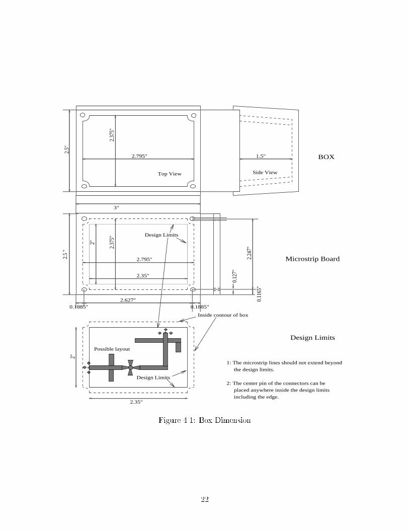
Top View Side View
2.795"
2.627"
2.795"
2.35"
2"
2.37
5"
2.5"
2.5
"
2.37
5"
2.35"
2"
Possible layout
the design limits.
including the edge.
Inside contour of box
3"
1.5"
2.24
7"
BOX
0.12
7"
0.1885"0.1885"
0.11
65"
Microstrip Board
Design Limits
1: The microstrip lines should not extend beyond
2: The center pin of the connectors can be
placed anywhere inside the design limits
Design Limits
Design Limits
Figure 4.1: Box Dimension
22
A 50 line of 1/4 of an inch should be reserved to attach the SMA Connector (SMA
launcher).
MINIMIZE the area of your circuit. The Quick Circuit fabrication time and therefore
tool-wear is proportional to the amount of copper to remove! Please minimize the
foot-print of your circuit. For the low-noise amplier the box constrains the size of the
layout.
Please set up an appointment with the TA before the Layout Approval by TA date
specied in your syllabus. to have your layout checked and approved for fabrication by the
TA.
Expect up to a week turn around for fabrication.
The circuits are all fabricated together in a single batch. Your design should
therefore be delivered to the Teaching Assistant by the Final Layout De-
livery date specied in your syllabus.
4.2 Fabrication Procedure
The fabrication of your circuit with Quick Circuit involves multiple steps which are performed
by the Teaching Assistant. First your layout is nalized with the addition of the connector
footprints and the transistor footprint determined and the circuit bound is determined. The
le is then converted in Gerber format. The fabrication process is manually designed from
your layout using a tool call Isolator. Finally the fabrication process is executed.
Your circuit built with the Quick-Circuit machine should already include all the transmission
lines and holes required and no additional drilling or cutting should be required. Therefore
the remaining fabrication steps are relatively few.
List of parts:
Microwave transistor
Microstrip board
2 SMA connectors
PNP biasing network (provided)
bias TEE are required for oscillators and LNA
Fabrication Procedure:
1. Solder the transistor using the soldering iron (see Appendix 5.4). Use a heat sink to
23

avoid damaging the transistor. The transistor leads need to be ush with the
microstrip board.
2. Fix the connectors on the circuit board. One of the four legs must be removed if this
has not been done. The connector NEEDs to be ush with the ground plane.
Solder the connectors using the soldering gun (see Appendix 5.4). Soldering to legs on
the ground plane should be sucient.
4.3 Measurement of Your Circuit.
Measurement procedure:
1. Make a 2 port calibration with the Network Analyzer or recall one saved on the HP
disk drive for the same test cables.
2. Amplier Biasing:
Connect Port 1 to the input of the amplier (base of the NPN). Connect Port 2 to
the output of the amplier (collector of the NPN). The bias network should have
the BNC connector labeled "base" connected to port 1 and the BNC connector
labeled "collector" connected to port 2.
Turn on the HP6237 power supply. The operating voltage should already be set
to 10.1 V on the lower scale of the power supply meter (Do not increase it as
this could damage the biasing network). [Note: The red banana cable should
be connected to +18 V and the black cable to COM. The meter switch should
indicate +18 V.]
Connect the NPN biasing network to the HP 6237A power supply. Respect the
polarity (red with red, black with black)! The read part of the banana plug should
be connected to +18 V and the black part of the banana plug to COM.
3. Measure and plot jS21j in dB versus frequency. At which frequency f0 is the maximum
gain? What is the 3dB bandwidth B? Measure and plot jS11j in dB.
4. Measure and plot jS11j and jS22j in VSWR units. Check how well the input and output
networks are matched at the operating frequency.
5. Trim the open stub to improve the matching if necessary. You could also increase the
stubs' length by soldering a piece of copper tape.
24

6. If you experience diculty (apparent noise) with the measurement of the scattering
parameters with the Network Analyzer the amplier might be unstable. You can
verify it with the spectrum analyzer. The amplier can be stabilized with a feedback
resistance between collector and emitter or a shunt resistance (in series with a ship
capacitor) between base and emitter or collector and emitter.
7. Measure the input power for which the power gain drops of 1 dB.
8. For low noise ampliers: Measure the noise gure at the design frequency .
4.4 Write Up
4.4.1 The Laboratory Report
Your report should include:
0. The complete laboratory 3 report sheet available in Appendix 5.10
1. 1. Smith Chart Design
2. ADS circuit le and plot of S11, S22 and S21 (dB).
3. The drawing of the amplier layout including all dimensions.
4. Plots of measured jS11j; jS22j; jS12j; and jS21j (dB or VSWR) versus frequencies.
5. Compare the measured and simulated data.
6. Discuss the design and fabrication problems encountered.
4.4.2 Poster Page
A poster page summarizing your design and experimental results should be included with
the report. This poster page should include:
Project Title
Your names
EE723, Fall Quarter 1995
25
A project abstract describing the circuit targeted, the design approach and the perfor-
mance obtained.
A gure or two with short captions comparing the measured and simulated (ADS)
circuit performance.
A gure showing the layout generated by ADS.
A prototype Poster page in latex will be made available in the directory:
~roblin/latex/ .
26

5. APPENDICES
5.1 How to Use ADS
The most current information for using ADS is available at:http://eewww.eng.ohio-state.edu/ads
Usually to start ADS the following commands are used:
source /apps/ads2002/Startup.EEhpads
TUTORIAL:
If you are new to ADS you should go through the OSU tutorial:http://eewww.eng.ohio-state.edu/ads/tutorial2.pdf
Check also our local ADS webpage: http://eewww.eng.ohio-state.edu/ads for accessto the online ADS manual and other various tutorials found on the web.
MOVING OR SHARING DESIGNS:
Note that if you are moving your design les to another directory (or want to share themwith someone else) you can copy both the .dsn and .ael les of the networks directory ofyour project directory. The .atf les are generated automatically.
IMPORTANT NOTE:
It is important not to exist ADS in an unconventional way. When you do ADS keeps runningin the background even if you log o. We have only ten user licenses and we quickly runout of them if such processes are running in the background. The consequence is that otherpeople (including yourself) stop being able to use ADS. Please exit ADS using the exitcommand in the Project menu.
If ever ADS dies or is exited unconventionaly you need to kill all the unix process which arestill running. For this purpose type:psor type:ps -ef j grep yourusername
Then kill the job number involving your name and hpeesof. For example by typing ps -ef jgrep roblin the user roblin obtained among otherthing:
roblin 14776 14775 0 Jan 5 pts/0 0:00 hpeesofviewer
To kill that job simply type:kill -9 14776
27

5.2 How to Use the Layout Tool
ADS allows for the automatic generation of the layout from the circuit design.
To generate the layout you must have both the schematic and layout windows open. In the
schematic window select the synchronize menu and the rst item on this menu. ADS will
highlight in red every circuit for which it has a corresponding layout or foot print. It does
not have a foot print for capacitors. ADS starts by Port 1 and asks you where you want to
locate it. Position (0,0) is just ne. The layout will stop whenever, starting from port 1,
ADS runs into a device for which it does not have a layout. If you run again synchronize it
will then ask for a new position (x,y) where to initiate the continuation of the layout. The
best is to instead introduce elements which specify a foot print. For example for a capacitor
you would use a chip capacitors. Simply place in parallel with the ideal capacitor a MGAP
(microstrip gap) element and specify the width of the gap (width of the capacitor).
Note that the synchronize tool requires that you make use of the discontinuities MSTEP,
MCROSS, MGAP, VIA2 and so on to establish a physical network. This is also required to
obtained a realistic simulation of your circuits as these discontinuities introduces parasitics
which impact the microwave performance of your circuit.
As you go through several layout trials you will want to RESET the layout window. For this
purpose go to the le menu and select: clear layout and then synchronize again to obtain
a new layout. Be careful if you synchronize in the layout window your schematic
will be updated! Save your schematic ahead of time to avoid an unwanted modication of
your schematic.
Sometimes the layout is not what you want. For example one can experience two lines
intersecting. In the layout window you can then click on all the items you want to move
together and then move them and rotate them where you want. All the editing commands
apply to these items.
The layout is really occuring on several layers. The metal (cond) layer is the most important
one for our process. However you need also to dene the bound (size) of the circuit. In the
Layout window go to the Draw menu and select the Select layer menu time. Select (you
might have to scroll down the menu) the bound layer (not bond!). Then again select the
Draw menu and select rectangle. Place your rectangle with the mouse. The Quick Circuit
machine will cut the contour of your circuit using the bound you specied. If your circuit is
to be placed in the box available refer to the section below discussing
Holes are also considered as a layer. There are automatically introduced by the via holes:
VIA2 (see below).
28

Ask you instructor for more information on the substrate you will be using. For the nal
Quick Circuit design we usually use a thin substrate of 30 or 45 mils to obtain smaller
microstrip linewidth. Changing the substrate MSUB aects the width of all the lines. Such
a change can be easily implemented in your schematic if you dene a variable say W1 for
microstrip lines of same width. Then you can select the value type of the width to be a
variable (instead of a parameter) and select this variable to be W1 in the value option
menu.
Via Holes:
Via holes are used to establish a connection to ground. They also aect the simulation
since a via hole behaves as an inductor. You need therefore to include them both for the
simulation and the layout. Use the model VIA2 available in the microstrip library. W is
the width of the square pad used on the top of the microstrip. The hole should be smaller
than the width of the pad.
So in summary to perform a layout you need to updage your schematic with MCROSS,
MSTEP, MGAP, VIA2, bias line (for active circuits) and so on to obtain a realistic design.
When you are done with your layout schedule an appointment with your instructor to discuss
your layout/schematics and simulation before the scheduled fabrication (see EE723 syllabus).
29

5.3 How to Use LineCalc
How to Start and Use LineCalc:
1. You can start LineCalc from the ADS Circuit window from the TOOLS menu.
2. We will most likely use LineCalc to synthesize a microstrip line. Click on Select... and
scroll down the menu to select MLIN (and not MCLIN) and click on OK.
3. Edit the various substrate parameters using the Modify Substrate key (you may need
to scroll the menu or make the window bigger): Er is the eective relative dielectric
constant, Mur is the permittivity (1.0), H is the thickness of the substrate, Hu is the
position of the cover (keep it large if there is none), T the thickness of the copper line
Cond is the copper line conductivity: (4:878 107!1m1, TanD is the loss tangent,
Rough is the ideal surface roughness (Rough=0 is a very good approximation).
4. Edit the component parameters. Select the frequency Freq targeted. Wall1 andWall2
are the distance of the microstrip line from the side metallic walls. Set Wall1 = 0 and
Wall2 = 0 to make them innite (no walls) except maybe if you are making a low
noise amplier going into a box.
5. Set the characteristic impedance ZO and eective electrical length E_Eff you wish to
obtain.
6. Click the up arrow to calculate the width W and length L of the microstrip line. Also
calculated are K_Eff the eective relative dielectric constant, the line attenuation A_DB
and the skin depth.
7. For more information use the on-line Help command.
30

5.4 Tips for Soldering
Tips for soldering the transistor:
1. Moisten the sponge of the soldering stand.
2. Turn on the soldering iron.
3. Set the temperature around 700oF.
4. The right light is blinking when the tip is hot.
5. Before soldering clean the soldering tip with the moisten sponge.
6. Fast soldering will prevent overheating of both the circuit and elements.
7. Avoid breathing the fumes.
8. Do not use too much solder.
9. When you solder the chip capacitor or resistor, one student can hold the element with
tweasers and the other solder it.
10. When you solder the center conductor of the connector, you should solder both sides
of the conductor.
11. Be careful when soldering the transistor on the copper tape. To prevent damaging
your transistor use a heat sink such as a metal clip or pliers.
Tips for soldering the connectors
To solder the SMA connectors to the microstrip board use the soldering gun. BE CARE-
FULL. You must plug it and press on the trigger to active it for the time you
are soldering ONLY.
The SAFETY PRECAUTIONS are:
1. Keep you soldering gun well away from all ammable material.
2. To avoid burns, always assume that the tip is hot.
3. Be sure the hot metal tip does not come in contact with the electrical power cord.
4. Before making any adjustment-removing or replacing a tip etc- make sure the gun is
unplugged and cool.
31

5. Release the trigger whenever the tip is not in contact with work. NEVER EVER tape
back the trigger.
6. Do not hold work in your hand if you can possibly avoid it. Use a vise, clamp or pliers.
7. Do not dip the tool into any liquid.
8. Many materials give o unpleasant fumes when heated-so always work in a well venti-
lated room.
9. Clean the tip by wiping it, when hot across a damp sponge or cloth- placed on a
non- ammable surface, NOT held in the hand.
10. AFTER USE, DISCONNECT the soldering gun. allow the tip to cool
completely, and store the tool in a safe place (out of reach of children).
11. Safety goggles are recommanded to prevent hot materials from entering the eyes.
Do not use much solder to hold the connectors. We intend to reuse these connectors.
32

5.5 Caring About Connectors
The relatively inexpensive SMA connectors we use are not made to be connected more than
a few times in their lifetime. You might notice gold particles on the white dielectric of the
cables and standards which will aect the quality of you calibration and measurement. In
such a case clean the cables and standards using a cotton swab and alcool. Here are some
general care and maintenance rules.
1. Do
a) Keep connectors clean
b) Extend sleeve or connector nut when you store it
c) Place plastic end-caps after you use it
d) Inspect all connectors carefully before every connection
e) Look for metal particles, scratches, dents when you inspect it
f) Align connectors carefully when you connect them
g) Make preliminary connection lightly
h) Turn connector nut only to tighten
i) Use a torque wrench for nal connection. Use the 5 lb-in torque wrench to connect
a male SMA to a female SMA or a female precision 3.5 mm. Use the 8 lb-in torque
wrench to connect a male precision 3.5 mm to female SMA connectors.
2. Do not
a) Touch mating plate surfaces
b) Set connectors contact-end down
c) Use a damaged connector
d) Apply bending force to connector
e) Overtighten preliminary connection
f) Twist or screw in connectors
g) Tighten past \break" point of torque wrench
33

5.6 AT42085 S-Parameters and Noise Parameters
! File AT42085
! Vce=8V Ic=10mA
! S parameters, Common Emitter
0.1 .72 - 50 26.52 152 .014 73 .90 -16
0.5 .66 -139 11.23 103 .035 36 .53 -32
1.0 .65 -168 5.95 84 .037 39 .45 -33
1.5 .65 175 4.06 71 .045 46 .43 -36
2.0 .65 163 3.06 60 .054 51 .42 -41
2.5 .66 157 2.51 55 .063 60 .42 -42
3.0 .68 149 2.07 46 .072 65 .41 -48
3.5 .68 141 1.79 38 .085 64 .43 -55
4.0 .69 133 1.57 29 .104 64 .45 -61
4.5 .69 125 1.41 21 .119 63 .46 -66
5.0 .69 114 1.28 12 .139 58 .47 -71
5.5 .71 103 1.17 3 .161 55 .44 -76
6.0 .75 91 1.07 -6 .177 49 .40 -85
! Noise Parameters, Common Emitter
!FREQ Fopt GAMMA OPT RN/Zo
!GHZ dB MAG ANG -
0.1 1.1 0.05 16 0.13
0.5 1.2 0.06 77 0.13
1 1.3 0.10 131 0.12
2 2.0 0.24 -179 0.11
4 3.5 0.46 -128 0.25
34

5.7 Computer Data Acquisition for 2-Port S-parameters
NOTE: A new improved data acquisition tool is now also available contact the
TA for additional information
Overview
The purpose of this document is to outline the necessary steps to acquire data from the
network analyzer for use in a program such as MATLAB or ADS. The HP 8753C network
analyzer communicates though the GPIB (General Purpose Interface bus) card installed in
the PC. A graphical interface for GPIB commands has been implemented in LabVIEW to
acquire data. To get started, set the network analyzer to Talker/Listener mode from the
LOCAL menu button.
Loading a Calibration from the PC
Double click on the SaveRecall.vi icon located on the Windows 95 desktop. Select Run from
the Operate menu. The red stop sign on the LabVIEW menu toolbar indicates when the
program is nished. When the program is nished, select Exit from the File menu. Press
the LOCAL menu button on the front panel of the network analyzer to regain control of it.
Saving Sparameter Measurements
Locate the Daq4SP.vi icon on the Windows 95 desktop. Double click on this icon to start
the data acquisition virtual instrument in LabVIEW. This programs allows up to four mea-
surements; use the scroll bar on the right side of the screen to view the rest of the panel.
The default selections of the Data Format and S Parameter controls are set to measure all
four S parameters in Smith Chart format. You can change the Destination File to the path
where the data is to be saved for a single measurement. Note that four separate les for data
will be created at the completion of the program. To perform a measurement select Run
from the Operate menu. The program may take some time to transfer the calibration les
to the network analyzer. If the le in the Destination File prompt currently exists another
dialogue will appear, click Replace to overwrite the le. Program execution can be halted at
anytime by pressing the red stop sign on the LabVIEW menu tool bar. After the program
has executed, press the LOCAL menu button on the network analyzer to regain control of
it. If you are not making any more measurements from LabVIEW then proceed through the
following menu sequence: MENU, TRIGGER MENU, CONTINUOUS. This will remove the
network analyzer from HOLD mode and allow you to make additional measurements from
the network analyzer.
Data Handling
The default path for the data is on the desktop in a folder called data, it should be the only
35

path used for hard drive data. For oppy disks, type a:\ file_name in the Destination File
indicator before program execution. Two methods of transporting your data to the Region
4 computers are described below.
(i) Using FTP to transfer les to Region 4 computers. To enable communications start
eXceed by selecting Programs/eXceed from the start menu located in the lower left corner
of the screen. Select Programs/eXceed/FTP from the start menu. Open a connection to
a remote account. Enter the server's name i.e. hector.eng.ohio-state.edu, username, and
password. Browse through the folders on the local system to nd the data le. On the
remote system click on the folder that the data le is to be copied to. Drag and drop the
le to the remote host, this can be accomplished by clicking and holding on the left mouse
button and moving the le to the appropriate location.
(ii) Ms-dos disks on Region 4 computers: Unix commands such as mdir, mcd, and mcopy
can be used to manipulate les on a oppy disk. For example, to retrieve the data from disk
type: mcopy a:/test.dat ~/my_dir/logmag.dat
Extensive documentation is available in the man pages on these commands.
Importing in ADS
Note that for 4 les (one per S-parameter) must be transferred. The function glue.pl available
in ~roblin/perl can be used to write the le in ADS format.
glue.pl S11.dat S12.dat S21.dat S22.dat > myfile.s2p
Importing in MATLAB
To load a data le into a vector in MATLAB use the load command. To separate the columns
of the resulting vector use a command similar to x = test(:,1), y = test(:,2).
36

5.8 Loading S-parameter data in ADS and MATLAB
In laboratory 3 you need to compare the S parameters measured for the device you designed
and fabricated with those you obtained with your simulation. This appendix describes several
way to do it:
To plot experimental data in ADS Move to the data directory of your project directory
(for example HPEESOF/ee723 prj)
cd
cd HPEESOF/ee723_prj/data
You are now going to create a le using an editor (for example vi or emacs) to store your S
parameter data. Call it for example mydata.s2p: The le should look like that
! Comments line: My data file ...
# GHz S MA R 50.0
! SCATTERING PARAMETERS :
2 0.95 -26 3.57 157 .04 76 .66 -14
3 0.93 -40 3.53 147 .05 69 .65 -20
4 0.89 -52 3.23 136 .06 62 .63 -26
Note that in the le above:
Comment lines start with !
The # line denes the units. In the example shown the Frequency is entered using
GHz. S indicates that S parameters are used. MA indicates that they are entered
using the amplitude (mag[Sij]) and the angle (ang[Sij]). R 50.0 means that 50 ohms is
the reference characteristic impedance.
The data are introduced in the following order:
Frequency mag[S11] ang[S11] mag[S21] ang[S21] mag[S12] ang[S12] mag[S22] ang[S22]
Once you have created your le and located it in the data directory you can load it in ADS
by doing the following:
While in the schematics window, click on the library menu and select the menu item:
Linear Data File Elements. In the right side of the dialogue box select then the item:
S2P(2-Port S-parameter File)
37

In the new dialogue box which then appears, click on Value Options. The le mydata you
have created before and which is located in the data directory should appear. Select it and
click on OK. Then click on Apply and the le name is loaded. Click on OK to introduce
this new device on your schematic. Then as usual you need to add two ports and a ground
terminal and save your schematic under a name before plotting the S-paramters in a test
window.
Note that you can save any les in ADS (circuit, layout) into a postscript le by clicking on
le and selecting print/plot setup. Select Graphics, File and Postscript Gray Scale and then
OK. Now when you select plot in the le menu you will be prompted for the name of the le
you want to save it to: e.g., mylayout.ps
Plotting ADS Data on MATLAB(Recommended Approach)
It might be more convenient to do the reverse: that is bring the ADS simulation data in
MATLAB. This gives you much more control. Bringing simulated data in ADS for compar-
ison with measured data can give you more control on the plot.
For this purpose you need to save your simulation data in a le while being in ADS. To do
so go in your test window in ADS. Click on Library, scroll down the menu and then click on
Output Files. Then select SNP (S-parameter File). In the value eld enter the name of the
le for example myle. ADS will automatically add an extension such as .s2p for a 2 port
device (myle.s2p), .s4p for a 4 port device (myle.s4p).
Locate the OFILE item in your test window and simulate. It would be convenient to select
a reasonable number of frequency points such as 20 points. The le will be created in the
data subdirectory of your project directory.
Before loading this le on MATLAB you need to clean it. Use an editor and remove the text
headers:
! Communications Design Suite 5.0 306 Aug 26 1994 (c) 1993 Hewlett-Packard
! Mon Nov 27 11:34:56 1995 lange_tb\Lange
# MHz S MA R 50.0000
! SCATTERING PARAMETERS :
Note that the header species the data type: S stands for scattering parameter, MA indicates
that the scattering parameters are represented by their magnitude and angle. 50 gives the
characteristic impedance.
For each frequency the data is presented in the following format for a 4 port:
38

freq magS11 angS11 magS12 angS12 magS13 angS13
magS21 angS21 magS22 angS22 magS23 angS23
magS31 angS31 magS32 angS32 magS32 angS33
magS41 angS41 magS42 angS42 magS42 angS43
For each frequency (freq) consolidate with your editor the three lines into a single one
freq magS11 angS11 magS12 angS12 magS13 angS13 magS21 angS21 magS22 angS22
magS23 angS23 magS31 angS31 magS32 angS32 magS32 angS33 magS41 angS41 magS42
angS42 magS42 angS43
To perform these task automatically you can use the script le s#p2text:
s#p2text <myfile.s4p >myfile.text
The les myle.s4p and myle.text and s#p2text in the ER4 directory
/tmp_mnt/user2/faculty/roblin/latex for you to inspect them.
Assume you saved your le myle.text You can now load your data in MATLAB using:
>> load myfile.text
Now the frequencies are stored in
>> myfile(:,1)
The amplitude of S11 is stored in
>> myfile(:,2)
To plot simply type:
>> plot (myfile(:,1),myfile(:,2))
To save into an encapsulated postscript le type:
>> print -deps2 myfile.eps
39

Some of you have several plots they would like to combine together in a single plot and
postscript le. This is easily done with MATLAB. Four small plots (2x2) would be generated
using:
>>subplot(2,2,1), plot (myfile(:,1),myfile(:,2))
>>subplot(2,2,2), plot (myfile(:,1),myfile(:,4))
>>subplot(2,2,3), plot (myfile(:,1),myfile(:,6))
>>subplot(2,2,4), plot (myfile(:,1),myfile(:,8))
Type help plot or help subplot to check how to set your titles and axes.
40

5.9 Active Biasing Circuit
(from Ralph S. Carson, High Frequency Ampliers, 1982)
An active biasing circuit is shown in Fig. 5.16a. Here, pnp transistoorQ1, assumed to operate
in its active region, helps stabilize the operating point of transistor Q2, hence the name active
biasing. The basic operation of the circuit is as follows. If IC2 increases, more voltage of the
polarity indicated in Fig. 5.16 appears across R3, and this decreases the forward bias for
the emitter-base circuit of Q1, so IE1 decreases. Since IC1 = IB2 = 1IE1, a decrease in IE1
causes IB2 to decrease. But a decrease in IB2 leads to a decrease in IC2, so this opposes the
increase in IC2 assumed originally. Therefore bias stabilization is achieved.
The analysis of the active biasing circuit cannot follow the T -equivalent method because of
the active device Q1. Instead, straightforward circuit analysis can be carried out after sub-
stituting an appropriate circuit model for each transistor, as shown in Fig. 5.16b. Neglecting
Ico, for Case I,we nd, from Fig. 5.16b
IC2 = 2IB2 = 21IE1
Since 1 ' 1, this becomes
IC2 ' 2IE1 (1)
Also,
IR3= IE1 + IC2 ' IE1 + 2IE1 = IE1(1 + 2)
Using KVL around the VCC R1R2 loop and substituting (1) = 1=(1+ ), we obtain
IR1(R1 +R2) + IE1
1
1 + 1
!R1 = VCC (2)
and, using KVL around the R2 R3 VBE1 loop yields
IR2(R2) IE1(1 + 2)R3 = VBE1 (3)
Solve 2 and 3 for IE1 and substitute that result into 1 to obtain, for negligible Ico,
IC2 ' (1 + 1)2hVCC
R2
R1+R2
VBE1
iR4 + (1 + 1)(1 + 2)R3
(4)
where R4 = R1R2=(R1 + R2). If (1 + 1)(1 + 2)R3 R4; IC2 is independent of 1 and
varies as 1=(1 + 2),and bias stabilization is obtained. It is seen that the collector current
41

IC2 does not depend on VBE2 because the current source 1IE1, in the simplied transistor
model is independent of VBE2.
Therefore for large 1 and 2 we have (1+ 1) (1+ 2) R4=R3 and the collector current
of the transistor Q2 (microwave transistor) is
ICC =VCC
R2
R1+R2
VBE1
R3
Q1
Q2
Port 2
E
CB
Port1
R
R
R
1
23
Vcc
BNC
E
Network Analyzer
DC bias DC bias
BNC
RFRF
HP 8753C
SMASMA
Vcc
Q2
R3
R2
R1
IR2 Cdecoupling
CdecouplingCdecoupling
RF in
Q1
I
I
I
I
RFChoke
RF Choke
C2
E1
R1
I IB1 B2
R3
MicrowaveTransistor
RF out
Figure 5.1: (a)Overal active biasing circuit and (b) active bias analysis
42

5.10 Laboratory Report Forms
43

Name:
Date:
EE 723 Adjunct Laboratory | LABORATORY #1 Report
Step 4) of Part I:
Center frequency: f0 =
Bandwidth: B =
S21(f0) dB =jS21(f0)jdB =
(Include S21 plot in appendix)
jS12(f0)jdB =
jS11(f0)j (SWR) =
jS22(f0)j (SWR) =
Step 5 of Part I:
Include the swept power gain compression plot in appendix.
jS21(Pin = 10dBm)j (in dB) =
Pin(1dB drop of jS21j) =
Step 6 of Part II:
Include the Noise Figure versus frequency plot in appendix. Noise Figure at 1.8 GHz (withPower on):
F (1.8 GHz) =
Minimum detectable input signal (See Gonzalez, p. 354):
Pi;mdsdBm =
Discussion/Comments:
44

Name:
Date:
EE 723 Adjunct Laboratory | LABORATORY #2 Report
Include the Smith Chart plots of S21; S12; S22; and S11 for the AT42085 from 300 kHz to 3GHz measured with the network analyzer.
Include a listing of the scattering parameters for the frequencies given in Appendix 5.6.
Using ADS compare in a single Smith Chart plot, all the measured scattering parameterswith those given in Appendix 5.6. Appendix 5.6 gives the procedure to load your data inADS.
45

Name:
Date:
EE 723 Adjunct Laboratory | PROPOSAL for LABORATORY #3
Project Title:
Design Goals:
Design Procedure:
List of parts:
1 AT42085 transistor
Duroid circuit board
2 SMA connectors
46

Name:
Date:
EE 723 Adjunct Laboratory | LABORATORY #3 Report
Amplier characteristics:
center frequency: f0 =
3dB bandwidth: B =
jS21(f0)jdB =
(Include S21 plot in appendix)
jS12(f0)jdB =
jS11(f0)j (SWR) =
jS22(f0)j (SWR) =
Optional: Include the swept power gain compression plot in appendix.
jS21(Pin = 10dBm)j (in dB) =
Pin ( - 1 dB drop of jS21j ) =
Noise Figure at 1.5 GHz (with Power on):
Minimum detectable input signal (See Gonzalez, p. 176):
Pi;mds =
47