computing surface 2
TRANSCRIPT

C omputing Surface 2
MK401SPARC (IO)Board
Specification

Computing Surface 2
The information supplied in this document is believed to be true but no liability is assumed for its use or for theinfringements of the rights of others resulting from its use. No licence or other rights are granted in respect ofany rights owned by any of the organisations mentioned herein.
This document may not be copied, in whole or in part, without the prior written consent of Meiko WorldIncorporated.
Copyright c�
1993 Meiko World Incorporated.
The specifications listed in this document are subject to change without notice.
Meiko, CS-2, Computing Surface, and CSTools are trademarks of Meiko Limited. Sun, Sun and a numericsuffix, Solaris, SunOS, AnswerBook, NFS, XView, and OpenWindows are trademarks of Sun Microsystems,Inc. All SPARC trademarks are trademarks or registered trademarks of SPARC International, Inc. Unix, UnixSystem V, and OpenLook are registered trademarks of Unix System Laboratories, Inc. The X Windows Systemis a trademark of the Massachusetts Institute of Technology. AVS is a trademark of Advanced Visual SystemsInc. Verilog is a registered trademark of Cadence Design Systems, Inc. All other trademarks are acknowledged.
Issue status: DraftPreliminaryReleaseObsolete
Circulation control:

1
OVERVIEW
The MK401 (SPARC/IO) is the first board in the new machine architecture. As such itincorporates several new devices and concepts. A complete mechanical redesign hasresulted in a card size of 14 inches by 15 inches. The Elan/Elite communicationsnetwork is supported, and a new supervisory structure based around the CAN(Control Area Network) serial bus protocol is implemented. All input/outputconnectors are brought to the front panel of the cards, removing the need for IO‘dongles’. Built-in SCSI drives are also supported with backplane SCSI wiring.
The board is MBus based with a single MBus (single node). On this MBus areplaced two full size MBus processor card sites. This allows two SPARC CPUs tobe supported, either as one dual processor card or two single processor cards. Alsoon the MBus is the Elan communication processor which has two Elan links to thebackplane. An MBus to SBus converter chip drives an SBus which has three singlesized SBus master card sites in addition to two SBus DMA controllers supporting anEthernet port and two SCSI ports. The SBus cards and one of the MBus cards havefront panel access space. A memory controller supports up to 128MBytes of errorchecked DRAM using 4Mbit DRAM technology. Support for 16Mbit DRAMs isincluded and allows a total of 512MBytes of DRAM on the node. An additionalcontroller supports an 8bit peripheral bus, the IO Bus, with a variety of devicesattached. These include a Boot ROM, real time clock, two serial ports, keyboard andmouse ports, an interface to the CAN bus and miscellaneous node control functions.
H0002–10M103.04 1

2
IMPLEMENTATION
This section gives some details about each of the major structural blocks of theMK401. Subsequent sections will give full details, register descriptions, addressmaps etc.
2.1 MBus and Processor SlotsThe MBus is fully level two compliant and runs at 40MHz. Support in the form ofbus request and grant lines and interrupt signals is provided for two processors. Thesecan either be on the same processor card or one on each card.
Each device attached to the MBus has a unique MBus ID. This is used to decodeaddresses at which the devices may be accessed. MBus processor slot 0 is givenMBus IDs 8 and 9, and slot 1 is given IDs 10 and 11. Note that most SPARCprocessor cards do not actually use these MBus ID signals but instead rely on softwareprogrammed registers. To allow each processor to establish a unique identity there isa register which each can read to determine which MBus request and grant line it isattached to. This register is described fully later.
H0002–10M103.04 2
2 Implementation
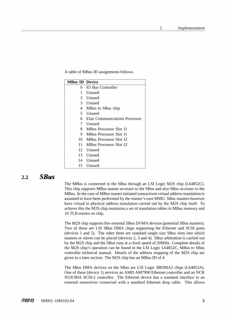
A table of MBus ID assignments follows.
MBus ID Device0 IO Bus Controller1 Unused2 Unused3 Unused4 MBus to SBus chip5 Unused6 Elan Communications Processor7 Unused8 MBus Processor Slot J19 MBus Processor Slot J1
10 MBus Processor Slot J211 MBus Processor Slot J212 Unused13 Unused14 Unused15 Unused
2.2 SBusThe MBus is connected to the SBus through an LSI Logic M2S chip (L64852C).This chip supports MBus master accesses to the SBus and also SBus accesses to theMBus. In the case of MBus master initiated transactions virtual address translation isassumed to have been performed by the master’s own MMU. SBus masters howeverhave virtual to physical address translation carried out by the M2S chip itself. Toachieve this the M2S chip maintains a set of translation tables in MBus memory and16 TLB entries on chip.
The M2S chip supports five external SBus DVMA devices (potential SBus masters).Two of these are LSI SBus DMA chips supporting the Ethernet and SCSI ports(devices 1 and 5). The other three are standard single size SBus slots into whichmasters or slaves can be placed (devices 2, 3 and 4). SBus arbitration is carried outby the M2S chip and the SBus runs at a clock speed of 20MHz. Complete details ofthe M2S chip’s operation can be found in the LSI Logic L64852C, MBus to SBuscontroller technical manual. Details of the address mapping of the M2S chip aregiven in a later section. The M2S chip has an MBus ID of 4.
The SBus DMA devices on the SBus are LSI Logic SBDMA2 chips (L64853A).One of these (device 1) services an AMD AM7990 Ethernet controller and an NCRN53C90A SCSI-2 controller. The Ethernet device has a standard interface to anexternal transceiver connected with a standard Ethernet drop cable. This allows
H0002–10M103.04 3
Computing Surface 2
connection to either thick or thin wire Ethernet. The SCSI-2 controller supports an8bit, single ended SCSI bus with connections at the backplane and a standard high-density SCSI socket on the front panel. This latter allows connection to external SCSIdevices such as CD-ROM drives and scanners. The second SBus DMA device (SBusdevice 5) has the similar SCSI-2 circuitry but without an Ethernet connection.
Termination for the SCSI bus must be provided for correct operation. On boardtermination can be enabled by a front panel recessed switch. If the SCSI bus is notused this termination must be used. If there are devices plugged into the bus then,for correct SCSI operation, the bus must be terminated at both ends. If devices areplugged into only either the backplane or the front panel then the on board terminationmust be used. If there are devices plugged into both front and back panels then theon board termination must be disabled.
2.3 DRAMThe memory controller used on the MK401 is the same as that in the SunSPARCstation10. This is the LSI chip, L64860, which uses a 128 bit wide data busfor fast memory accesses. The device supports single bit error correction, two biterror detection and multiple bits within a nibble detection. The device drives anarray of 16, 36bit wide, SIMMs identical to the ones used in the TwinEngine on theexisting MK083 product. The array is constructed as 4 groups of 4 SIMMs. Withineach group the SIMMs must be identical, but there is no requirement for the groupsto be the same. SIMMs can be either 4Mbit DRAM or 16Mbit DRAM technology,either single or double sided. This means that the minimum memory is 16MBytes andthis can be upgraded in 16MByte chunks to 128MBytes and then 64MByte chunksto 512MBytes. Section 6 gives more details about the various memory optionsavailable.
Writes to memory of less than 64bits width are automatically turned into read-modify-write cycles to the array. All MBus transaction sizes and Level-1 and Level-2transaction types are supported.
Memory accesses are error-checked with all single-bit errors being corrected. Errorsof two or more bits are uncorrectable and will cause a synchronous MBus erroracknowledgement to the MBus cycle. Single bit errors can be corrected and willreturn a normal MBus acknowledge. Their occurrence can be signalled with a level15 interrupt to the processors. This allows error logging and scrubbing operationsto be carried out. Error fault information is available for all single and multi-biterrors in registers within the memory controller. Kernel software can advise the boardcontroller of the occurrence of uncorrectable memory errors by sending a messageover the CAN bus. This can be used to log error information and cause a visible statuschange on the front panel LEDs.
H0002–10M103.04 4
2 Implementation
2.4 IO BusThe IO Bus is a general purpose 8-bit slave only bus designed to allow easyconnection of minor peripherals to the MBus. It is provided in this implementationby the LSI chip, L64851. There are several devices connected to this bus:
• An EPROM or Flash EPROM of up to 512KBytes. This holds the bootstrapprograms, ie. OpenBoot and Meiko Diagnostics.
• A realtime clock module with 8KBytes of battery backed SRAM. This holdsconfiguration information and node fault logs. It is software compatible with themodule used on SPARCstations.
• Two dual UART devices for connection to Keyboard, Mouse and two generalpurpose serial ports. These are the same as used on SPARCstations.
• Board and node control registers as follows:
• Interrupt request control for each processor.
• Free running timers for interrupt levels 10 and 14 to the processors.
• CAN interface chip to the control serial bus.
• MBus grant readback register.
• Node "Reset Me" request register.
• LED bargraph register.
• Asynchronous error interrupt status latches.
• Physical board ID register.
A brief description of each device follows. For details of address map allocationsection 3.
2.4.1 Boot ROMThe code in this ROM is read by both processors on startup. This code must performall the hardware initialisation, initial page table construction and booting of vmunixfrom the desired device. Note that since both processors start up together and accessthe same code a check will need to be made of the MBus grant line register. Onceeach processor is identified, processor 0 can continue with the hardware setup whileprocessor 1 idles. When processor 0 finishes it can wake processor 1 by issuing it asoftware interrupt.
H0002–10M103.04 5

Computing Surface 2
Board jumpers JP1 and JP2 allow the use of Flash EPROM in the Boot ROM socket.This feature is recommended only for Meiko internal software development. For thisreason the jumpers are Zerohm links soldered to pads on the underside of the board todissuade user alteration. Details of the Flash EPROM programming mechanism canbe found in the AMD data sheet for part Am28F020. This is included in AMD’s databook "CMOS Memory Products" of 1991. Location of the Boot ROM in the MBusphysical memory map is given in section 3.
2.4.2 Real Time ClockThe Real Time Clock used on the MK401 is the Mostek/SGS-Thompson partMK48T08. This is an 8KByte version of the earlier MK48T02 used on SunSPARCstations. The extra RAM is useful for logging of system failure data suchas Uncorrectable multi-bit errors. Detailed information about each fatal crash can bestored along with a date-stamp. In addition a log of time powered up could be keptalong with an audit trail of board manufacture tests and modifications.
The Clock module updates several of the RAM registers once every second. Themodule contains features for calibration to offset crystal frequency drift with time.year, month, date, day, hour, minute and second information is available.
Details of the locations of the various registers are included in section 3. For detailson programming the clock see the SGS-Thompson data sheet on the MK48T08.
2.4.3 Serial PortsThere are two Dual UARTs of type Z85C30 by AMD on the IO Bus. One chipreceives data from the keyboard and mouse connector on the front panel, the otherhandles to two RS232 serial ports also on the front panel. In the absence of a keyboardand frame buffer the bootstrap code has an option to direct console IO to serial portA.
These serial ports are clocked at 4.9152MHz and are thus theoretically capable ofup to 76.8KBaud. In practice 38.4KBaud is achievable. Note that both serial portA and serial port B use the same 25-way ‘D’ connector. Thus port A supports fullsynchronous and asynchronous operation and has a full set of modem control lines,whereas port B has a more limited set and only supports asynchronous operation.
Full details of the locations of the registers on the serial port controllers are includedin section 3. For details on programming the Z85C30 see the AMD publication"Z85C30 Serial Communications Controller. Technical Manual."
H0002–10M103.04 6
2 Implementation
2.4.4 Interrupt ControllerThe MK401 has many sources of interrupts to the SPARCs. These are assignedto various priority levels and given to the Interrupt Controller. There is a separatecontroller for each processor, to enable interrupt handling to be effectively sharedbetween the processors. Each controller is implemented in a large PAL, full detailsof which are given in section 5. The controller has the following major features:
• Masks for all hardware generated interrupts.
• Software interrupts on six levels using a multi-processor compatible set/clearregister structure. This allows one processor to interrupt the other by writing onceto a single memory location, without having to do a read-modify-write cycle whichis subject to being broken by the other processor. Supported levels are 1, 4, 6, 12,13 and 15.
• Latches triggered by the outputs of the free running timers. These capture the timerpassing zero event and cause an interrupt to the processor. When the interrupthandler accepts the interrupt and clears the request it resets this latch.
• Priority encoder to generate the 4bit encoded interrupt level that is passed to theSPARC processor module.
2.4.5 Periodic Interrupt TimersPeriodic interrupts are used for maintaining the Unix clock and kernel profiling. Eachprocessor has a separate timer chip (an AM82C54) which has three free runningtimers integrated. Timer 0 is used for the lower priority clock ticks. This timercounts from a set value down to zero, decrementing once every 3.2us and generatinga level 10 interrupt on reaching zero. Timer 1 is used for higher priority interruptsfor kernel profiling. This timer decrements once every 0.8us and generates a level 14interrupt on reaching zero.
Note that the Timer 0 for processor 0 generates the level 10 interrupts forprocessor 1 as well. This removes the need to initialise Timer 0 in the other timerchip.
Full details of the registers in the timer chips are given in the AMD data sheet for theAm82C54. Memory locations on the MK401 are given in section 3.
H0002–10M103.04 7
Computing Surface 2
2.4.6 CAN InterfaceThe SPARC processors have direct access to the control serial bus with their ownCAN bus interface chip. This is intended to be used only by the node that is actingas machine controller. All MK401 SPARC/IO nodes will have the capability ofbecoming machine controller. The CAN chip has the capacity of generating a largenumber of level 2 interrupts and thus should be disabled on all nodes other than thedesignated machine controller to avoid impacting CPU performance.
The CAN controller is a Phillips PCA82C200 device and full details of the chip aregiven in the Phillips data sheet accompanying it. Placement of its registers within theMBus physical memory map is given in section 3.
2.4.7 Miscellaneous RegistersThis section describes the various registers used to control the node’s operation.Address map positions are summarised in section 3.
2.4.7.1 MBus Grant ReadbackThis is a single eight bit read only register, visible by both SPARC processors. Thereare two bit fields as follows:
[3:0] Bits [3:0] are used to carry the active low MBus grant signals for this MBustransaction. An MBus master device can thus read this register to determineits unique ID. The bit that is clear when read is given by the following list:
0 MBus Processor 01 MBus Processor 12 Elan Communications Processor3 SBus Master accessing MBus.
[7:4] These four bits are unused and will return undefined values if read.
2.4.7.2 Node reset requestThis is a single eight bit write-only register accessible by both processors. Bits [7:1]are reserved and should be written as ones. Bit zero, when written as zero, causesa Node reset to be generated. During the reset process this register is restored to itsinactive state.
H0002–10M103.04 8

2 Implementation
2.4.7.3 LED BargraphThis is a single sixteen bit read/write register also accessible as two eight bit registers,visible to both processors. Bits [15:0] drive the sixteen module front panel LEDsto generate a performance/load Bargraph display. A zero should be written at a bitlocation to illuminate the corresponding LED. This register is set to all ones during anode reset operation.
2.4.7.4 Asynchronous error status latchThis is a four bit read only latch, which is cleared when written to. The bits are setwhen an asynchronous MBus or SBus fault or Memory error occurs and will cause amaskable level 15 interrupt to the SPARCs. The bits are defined as follows:
0 Uncorrectable multi-bit memory error or, when enabled, correctable single biterrors also.
1 MBus to SBus asynchronous transaction fault
2 Asynchronous Fault flagged by a slave MBus device in an MBus slot.
3 Backplane power failure signal asserted.
[7:4] These bits are unused and will have undefined values when read.
2.4.7.5 Physical board locationThis is a 16 bit read only register visible by both processors used to find the physicallocation of the MK401 card in the entire system. A twelve bit Slot ID is uniquelydefined for every card slot in the machine and is read at this location, at the upper12 bits of the halfword. The least significant nibble contains the node number on thecard, which in the case of the single node MK401 is always zero.
H0002–10M103.04 9

3
MBUS PHYSICAL ADDRESS MAP
This section gives the mapping of memory and peripherals into the MBus physicaladdress space. All addresses are in hexadecimal, all locations are word wide unlessotherwise stated in the notes. The following notes are associated with some of theitems in the tables:
1 Memory banks are spaced 64MBytes apart. If less than 64MBytes of memory ispresent in each bank, it will appear echoed throughout the 64MByte.
2 These locations are byte wide and are mapped into all 4 bytes of a word. Careshould be taken to generate correct byte-wide accesses to the least significant byteof the word in order to maintain future compatibility.
3 These locations are byte-wide memory, mapped into contiguous byte locations.Word or halfword accesses will be automatically mapped into several successivebyte-wide accesses.
4 These locations are byte sized registers which are only mapped into the mostsignificant byte of a halfword. To ensure comparability with other boards onlybyte accesses at the correct address should be used.
5 These locations are byte sized registers which are only mapped into theleast significant byte of the word. To conserve MBus bandwidth and ensurecomparability with other boards only byte wide accesses at the correct addressshould be used.
6 These locations are halfword sized registers which are only mapped into theleast significant halfword of the word. To conserve MBus bandwidth and ensurecompatibility with other boards only halfword wide accesses at the correct addressshould be used.
7 These locations form a double-word register.
H0002–10M103.04 10

3 MBus Physical Address Map
DRAM and SBus SlotsMBus Address Usage Rd/Wr Note000000000 64MB Memory in bank 0 RW 1004000000 64MB Memory in bank 1 RW 1008000000 64MB Memory in bank 2 RW 100c000000 64MB Memory in bank 3 RW 1010000000 64MB Memory in bank 4 RW 1014000000 64MB Memory in bank 5 RW 1018000000 64MB Memory in bank 6 RW 101c000000 64MB Memory in bank 7 RW 1020000000 to dffffffff Unused (MBus Timeout)e00000000 to e0fffffff SBus Slot 1 (J11) RWe10000000 to e1fffffff SBus Slot 2 (J12) RWe20000000 to e2fffffff SBus Slot 3 (J13) RW
H0002–10M103.04 11

Computing Surface 2
SBus DMA chip B and SCSIMBus Address Usage Rd/Wr Notee30000000 SBus DMA_B ID register (=
0xfe810102)R
e30000004 to e303fffff Unused (Echoes of above)e30400000 SBus DMA_B Control/Status Register RWe30400004 SBus DMA_B (Next)AddressCounter RWe30400008 SBus DMA_B (Next)ByteCount RWe3040000c Reserved for testing M2Se30400010 to e307fffff Unused (Echoes of above)e30800000 SCSI_B Transfer Count Low RW 1e30800004 SCSI_B Transfer Count High RW 2e30800008 SCSI_B FIFO Data RW 2e3080000c SCSI_B Command RW 2e30800010 SCSI_B Status R 2e30800010 SCSI_B Destination Bus ID W 2e30800014 SCSI_B Interrupt R 2e30800014 SCSI_B Select/Reselect Timeout W 2e30800018 SCSI_B Sequence Step R 2e30800018 SCSI_B Synchronous Period W 2e3080001c SCSI_B FIFO Flags R 2e3080001c SCSI_B Synchronous Offset W 2e30800020 SCSI_B Configuration 1 RW 2e30800024 SCSI_B Clock Conversion Factor W 2e30800028 SCSI_B Test mode W 2e3080002c SCSI_B Configuration 2 RW 2e30800030 to e3080003c SCSI_B Reservede30800040 to e30bfffff Unused (Echoes of above)e30c00000 to e3fffffff Reserved (Read Undefined)
H0002–10M103.04 12
3 MBus Physical Address Map
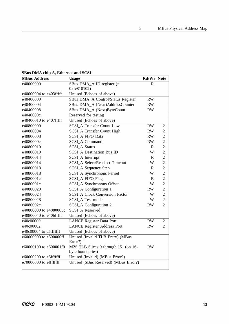
SBus DMA chip A, Ethernet and SCSIMBus Address Usage Rd/Wr Notee40000000 SBus DMA_A ID register (=
0xfe810102)R
e40000004 to e403fffff Unused (Echoes of above)e40400000 SBus DMA_A Control/Status Register RWe40400004 SBus DMA_A (Next)AddressCounter RWe40400008 SBus DMA_A (Next)ByteCount RWe4040000c Reserved for testinge40400010 to e407fffff Unused (Echoes of above)e40800000 SCSI_A Transfer Count Low RW 2e40800004 SCSI_A Transfer Count High RW 2e40800008 SCSI_A FIFO Data RW 2e4080000c SCSI_A Command RW 2e40800010 SCSI_A Status R 2e40800010 SCSI_A Destination Bus ID W 2e40800014 SCSI_A Interrupt R 2e40800014 SCSI_A Select/Reselect Timeout W 2e40800018 SCSI_A Sequence Step R 2e40800018 SCSI_A Synchronous Period W 2e4080001c SCSI_A FIFO Flags R 2e4080001c SCSI_A Synchronous Offset W 2e40800020 SCSI_A Configuration 1 RW 2e40800024 SCSI_A Clock Conversion Factor W 2e40800028 SCSI_A Test mode W 2e4080002c SCSI_A Configuration 2 RW 2e40800030 to e4080003c SCSI_A Reservede40800040 to e40bfffff Unused (Echoes of above)e40c00000 LANCE Register Data Port RW 2e40c00002 LANCE Register Address Port RW 2e40c00004 to e5fffffff Unused (Echoes of above)e60000000 to e600000ff Unused (Invalid TLB Entry) (MBus
Error?)e60000100 to e600001f0 M2S TLB Slices 0 through 15. (on 16-
byte boundaries)RW
e60000200 to e6fffffff Unused (Invalid) (MBus Error?)e70000000 to effffffff Unused (SBus Reserved) (MBus Error?)
H0002–10M103.04 13

Computing Surface 2
Memory ControllerMBus Address Usage Rd/Wr Notef00000000 Memory Enable RWf00000004 Memory Delay RWf00000008 Fault Status R(W)f0000000c Video Config RWf00000010 Fault Address 0 Rf00000014 Fault Address 1 Rf00000018 ECC Diagnostics RWf0000001c to f0fffffff Unused (Read undefined)f00000000 to fefffffff Unused (No response) (MBus Timeout)
H0002–10M103.04 14

3 MBus Physical Address Map
Boot ROM, Serial Ports, Real Time Clock, MiscellaneousMBus Address Usage Rd/Wr Noteff0000000 to ff007ffff Boot ROM (512KByte). (Writeable only when
Flash ROM installed and jumpers JP1 and JP2 arein the correct positions. See Flash ROM data sheetfor details of command port structure.)
R(W) 3
ff0080000 to ff00fffff Unused (Boot ROM Echo)ff0100000 to ff0100007 Serial Port Controllerff0100000 Control Registers port B RW 4ff0100002 Data Buffer port B RW 4ff0100004 Control Registers port A RW 4ff0100006 Data Buffer port A RW 4ff0100008 to ff01fffff Unused (Serial Port Echoes)ff0200000 to ff0200007 Keyboard and Mouse Port Controllerff0200000 Control Registers mouse port RW 4ff0200002 Data Buffer mouse port RW 4ff0200004 Control Registers keyboard port RW 4ff0200006 Data Buffer keyboard port) RW 4ff0200008 to ff02fffff Unused (Keyboard and Mouse Port
Echoes)ff0300000 to ff0301fff Real Time Clock module and 8KByte
SRAMRW 3
ff0302000 to ff03fffff Unused (RTC Echoes)ff0400000 to ff06fffff Unused (MBus Error)ff0700000 Node Reset Request W 5ff0700004 to ff07001ff Unused (Echoes)ff0700200 MBus Grant readback R 5ff0700204 to ff07003ff Unused (Echoes)ff0700400 Physical Slot Identifier R 6ff0700404 to ff07005ff Unused (Echoes)ff0700600 LED Bargraph RW 6ff0700604 to ff07007ff Unused (Echoes)
H0002–10M103.04 15
Computing Surface 2
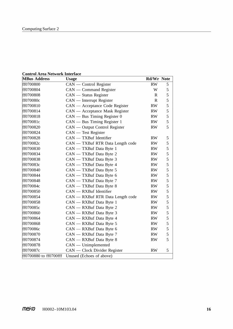
Control Area Network InterfaceMBus Address Usage Rd/Wr Noteff0700800 CAN — Control Register RW 5ff0700804 CAN — Command Register W 5ff0700808 CAN — Status Register R 5ff070080c CAN — Interrupt Register R 5ff0700810 CAN — Acceptance Code Register RW 5ff0700814 CAN — Acceptance Mask Register RW 5ff0700818 CAN — Bus Timing Register 0 RW 5ff070081c CAN — Bus Timing Register 1 RW 5ff0700820 CAN — Output Control Register RW 5ff0700824 CAN — Test Registerff0700828 CAN — TXBuf Identifier RW 5ff070082c CAN — TXBuf RTR Data Length code RW 5ff0700830 CAN — TXBuf Data Byte 1 RW 5ff0700834 CAN — TXBuf Data Byte 2 RW 5ff0700838 CAN — TXBuf Data Byte 3 RW 5ff070083c CAN — TXBuf Data Byte 4 RW 5ff0700840 CAN — TXBuf Data Byte 5 RW 5ff0700844 CAN — TXBuf Data Byte 6 RW 5ff0700848 CAN — TXBuf Data Byte 7 RW 5ff070084c CAN — TXBuf Data Byte 8 RW 5ff0700850 CAN — RXBuf Identifier RW 5ff0700854 CAN — RXBuf RTR Data Length code RW 5ff0700858 CAN — RXBuf Data Byte 1 RW 5ff070085c CAN — RXBuf Data Byte 2 RW 5ff0700860 CAN — RXBuf Data Byte 3 RW 5ff0700864 CAN — RXBuf Data Byte 4 RW 5ff0700868 CAN — RXBuf Data Byte 5 RW 5ff070086c CAN — RXBuf Data Byte 6 RW 5ff0700870 CAN — RXBuf Data Byte 7 RW 5ff0700874 CAN — RXBuf Data Byte 8 RW 5ff0700878 CAN — Unimplementedff070087c CAN — Clock Divider Register RW 5ff0700880 to ff0700fff Unused (Echoes of above)
H0002–10M103.04 16
3 MBus Physical Address Map
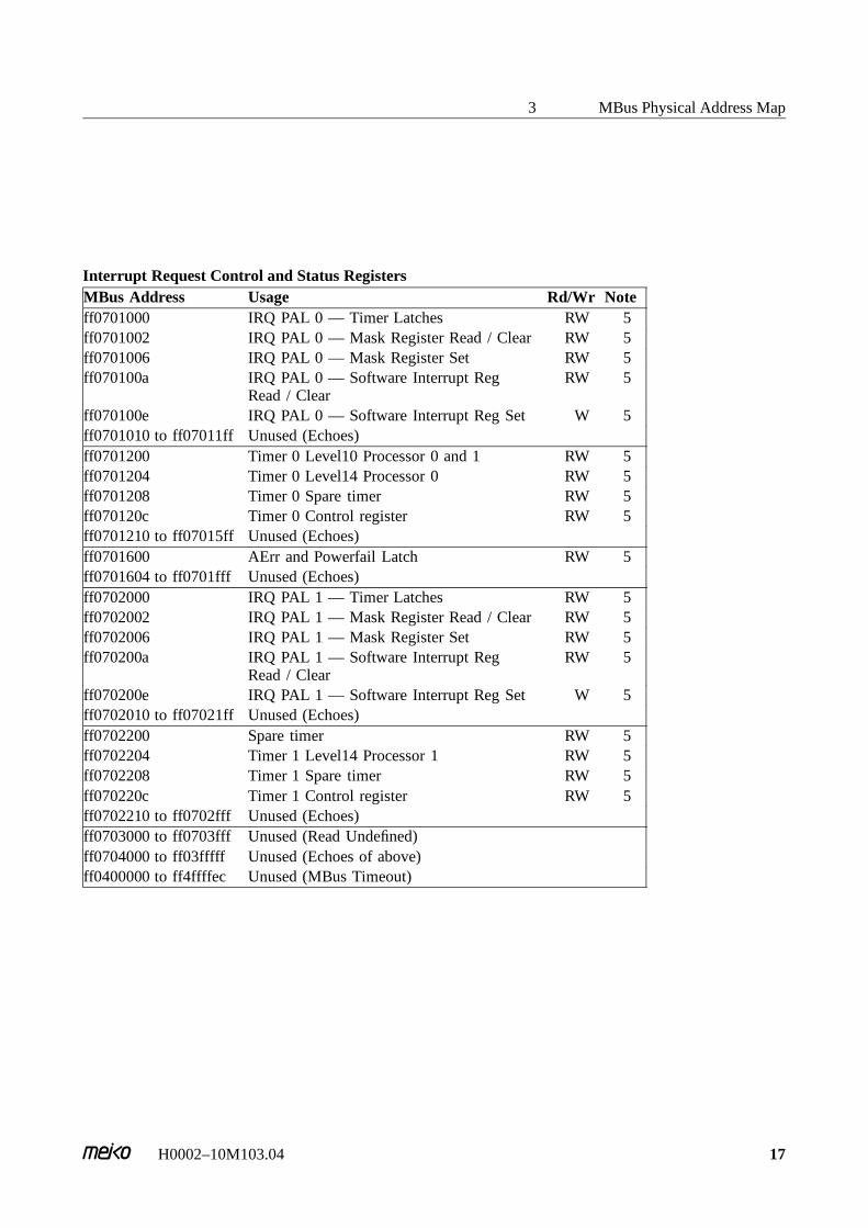
Interrupt Request Control and Status RegistersMBus Address Usage Rd/Wr Noteff0701000 IRQ PAL 0 — Timer Latches RW 5ff0701002 IRQ PAL 0 — Mask Register Read / Clear RW 5ff0701006 IRQ PAL 0 — Mask Register Set RW 5ff070100a IRQ PAL 0 — Software Interrupt Reg
Read / ClearRW 5
ff070100e IRQ PAL 0 — Software Interrupt Reg Set W 5ff0701010 to ff07011ff Unused (Echoes)ff0701200 Timer 0 Level10 Processor 0 and 1 RW 5ff0701204 Timer 0 Level14 Processor 0 RW 5ff0701208 Timer 0 Spare timer RW 5ff070120c Timer 0 Control register RW 5ff0701210 to ff07015ff Unused (Echoes)ff0701600 AErr and Powerfail Latch RW 5ff0701604 to ff0701fff Unused (Echoes)ff0702000 IRQ PAL 1 — Timer Latches RW 5ff0702002 IRQ PAL 1 — Mask Register Read / Clear RW 5ff0702006 IRQ PAL 1 — Mask Register Set RW 5ff070200a IRQ PAL 1 — Software Interrupt Reg
Read / ClearRW 5
ff070200e IRQ PAL 1 — Software Interrupt Reg Set W 5ff0702010 to ff07021ff Unused (Echoes)ff0702200 Spare timer RW 5ff0702204 Timer 1 Level14 Processor 1 RW 5ff0702208 Timer 1 Spare timer RW 5ff070220c Timer 1 Control register RW 5ff0702210 to ff0702fff Unused (Echoes)ff0703000 to ff0703fff Unused (Read Undefined)ff0704000 to ff03fffff Unused (Echoes of above)ff0400000 to ff4ffffec Unused (MBus Timeout)
H0002–10M103.04 17

Computing Surface 2
MBus to SBus Chip, Elan Communications Processor and MBus Slot SlavesMBus Address Usage Rd/Wr Noteff4fffff0 M2S Virtual Address Table Base Address RWff4fffff4 M2S IO/MMU Control register RWff4fffff8 M2S Error/Status register Rff4fffffc M2S — MBus ID Register Rff5000000 to ff6f7ffff Unused (MBus Timeout)ff6f80000 to ff6ffdfff ELAN Command port area RWff6ffe000 to ff6ffffbf ELAN Hush register area RWff6ffffc0 ELAN Clock Hi RWff6ffffc4 ELAN Clock Hi Rff6ffffc8 ELAN Clock Lo RWff6ffffcc ELAN Clock Lo Rff6ffffd0 ELAN Alarm RWff6ffffd4 ELAN Alarm Rff6ffffd8 ELAN Interrupt Rff6ffffdc ELAN Interrupt Rff6ffffe0 ELAN Clock Hi R 7ff6ffffe4 ELAN Clock Lo (For 64bit accesses) R 7ff6ffffe8 ELAN Main Proc. Interrupt Mask RWff6ffffec ELAN Main Proc. Interrupt Mask Rff6fffff0 ELAN Control register RWff6fffff4 ELAN Control register Rff6fffff8 MBus Port ID register for ELAN Chip Rff6fffffc MBus Port ID register for ELAN Chip Rff7000000 to ff7ffffff Unused (MBus timeout)ff8000000 to ff9ffffff Used by MBus slave device in MBus Slot
0ffa000000 to ffbffffff Used by MBus slave device in MBus Slot
1ffc000000 to fffffffff Unused (MBus timeout)
H0002–10M103.04 18

4
NODE CONTROL STRUCTURE
This section gives more detail on the control circuitry used to monitor and supervisethe operation of the node in a system. It details the function of the controlmicroprocessor and how it interfaces with the SPARC.
4.1 Control Microprocessor OverviewThe MK401 uses a Hitachi micro-controller to implement basic node controlfunctions. The controller is a member of the H8/500 series of single chip micros,containing 2KBytes of RAM and 32KBytes of EPROM as well as a number ofperipherals, IO ports, timers etc. The device is a H8/534 which has a 16-bit RISCbased CPU core. On-chip peripherals include 9 IO ports of which 3 are used byan external address and data bus for off-chip peripherals and memory. Other on-chip devices include two serial ports, 3 16-bit timers and one 8 bit one, pulse-widthmodulated outputs, analogue-to-digital converters etc. Much of this remains unusedon the MK401, however the chip and family has the potential to perform morecomplex tasks on future boards.
The H8 controller is responsible for performing the following actions:
• Monitoring of the CAN bus to detect messages addressed to this node and act onthem.
• Monitoring of the CAN bus to detect status and watchdog messages from the localnode and interpret them.
• Monitoring of the SPARC processor performance/load LED Bargraph signals tomake this information available remotely over the CAN bus.
• Placing the node in reset when directed to by CAN bus messages.
• Reporting physical slot ID over the CAN bus to allow the physical location of aboard to be located. Especially useful in very large systems.
• Recoding of the node status information to drive the two front-panel status LEDs.
H0002–10M103.04 19
Computing Surface 2
Most of the node to board control information flow goes over the CAN bus. Othersignals are the Slot ID, Bargraph lines and a node reset output from the H8. The H8also controls the front panel LEDs.
4.2 H8 IO Port AssignmentsEach subsection in this section is devoted to a particular IO port of the controller andgives a list of the signals connected to the port with some description of how they areused.
4.2.1 Port 10 This output carries the 10MHz H8 clock ‘Phi’.4:1 Slot-ID[11:8] inputs.5 notIRQ0 input from CAN interface chip. This can be used to trigger
a preprogrammed transfer of data to or from the CAN chip. See theH8 manual section 5 "Interrupt Controller" and section 6 "Data TransferController" for more information.
7:6 Unused IO.
Three registers are associated with Port 1 and should be programmed as follows.
P1DDR Port 1 data direction register should have 8’b00000001 programmed. Thissets unused IOs to inputs.
P1DR Carries the current input data.
SYSCR1 System Control register 1. Should be set to the value 8’b00100000 toenable the notIRQ line.
4.2.2 Port 2This port is used to carry strobes and select lines to the off-chip peripherals. Itsfunction is set automatically and no programming of the control registers P2DDRand P2DR is required.
0 This output carries the notAddressStrobe signal.1 This output carries the ReadnotWrite signal.2 This output carries the notDataStrobe signal.3 This output carries the notRead strobe.4 This output carries the notWrite strobe.
H0002–10M103.04 20

4 Node Control Structure
4.2.3 Port 3This port carries the eight bits of the data bus to off-chip peripherals. Its function isset automatically and no programming of the control registers P3DDR and P3DR isrequired.
4.2.4 Port 4This port carries the eight least significant bits of the address bus to off-chipperipherals. Its function is set automatically and no programming of the controlregisters P4DDR and P4DR is required.
4.2.5 Port 5This port carries the eight most significant bits of the data bus to off-chip peripherals.Its function is set automatically if off-chip ROM is enabled (See description forJP3 and JP4 in section 6). If on-chip ROM is used then P5DDR must be set to8’b11111111. No programming of the data register P5DR is required.
4.2.6 Port 60 Unused IO.1 This output, when low, causes the MK401 node to be reset.2 This signal drives the yellow front panel LED. The LED is illuminated
when the signal is low.3 This signal drives the green front panel LED. The LED is illuminated
when the signal is low.
Two registers are associated with Port 6 and should be programmed as follows.
P6DDR Port 6 data direction register should have 8’b00001110 programmed. Thissets unused IO to input.
P6DR The output pins are set to the value in this register.
4.2.7 Port 7This eight bit port is used to carry the low eight bits of the Slot ID value, Slot-ID[7:0].
Two registers are directly associated with Port 7 and should be programmed asfollows.
P7DDR Port 7 data direction register should have 8’b00000000 programmed.
P7DR Carries the data input on the pins.
H0002–10M103.04 21
Computing Surface 2
Other register bits have a bearing on Port 7s operation and should be programmed asfollows. See the H8 manual section 10 "16-Bit Free Running Timers" and section 11"8-Bit Timer" for more details on these registers.
FRT1.TCR.OEA Output Enable A of the Timer Control Register of FreeRunning Timer channel 1. This bit must be clear to enablenormal Port 7.7 operation.
FRT3.TCR.OEB Output Enable B of the Timer Control Register of FreeRunning Timer channel 3. This bit must be clear to enablenormal Port 7.6 operation.
FRT2.TCR.OEB Output Enable B of the Timer Control Register of FreeRunning Timer channel 2. This bit must be clear to enablenormal Port 7.5 operation.
FRT1.TCR.OEB Output Enable B of the Timer Control Register of FreeRunning Timer channel 1. This bit must be clear to enablenormal Port 7.4 operation.
TMR.TCR.CCLR1:0 These two bits of the Timer Control Register of the 8-bitTimer can be both set to one to enable resetting of thecounter from an input on Port 7.3. This must be disabled(by clearing one or both of these bits) to allow normaloperation of Port 7.3.
FRT2.ICR The count in Free Running Timer 2 is captured to its InputCapture Register on edges of the signal on Port7.2. Sincethis signal has no special time relationship to the H8, thevalue in the ICR will be meaningless.
FRT1.ICR The count in Free Running Timer 1 is captured to its InputCapture Register on edges of the signal on Port7.1. Sincethis signal has no special time relationship to the H8, thevalue in the ICR will be meaningless.
TMR.TCR.CKS2:0 These three bits of the Timer Control Register of the 8-bitTimer can be set to select Port7.0 as the clock signal forthe 8-bit Timer. Since the signal on Port7.0 has no timingsignificance to the H8, this should not be done.
H0002–10M103.04 22

4 Node Control Structure
4.2.8 Port 8This eight-bit port is used to monitor the low eight bits of the BarGraph value,notBAR[7:0].
Port 8 has no Data direction register (being input only) so the only register of interestis P8DR, which reflects the state of the input pins.
4.2.9 Port 9This eight-bit port is used to monitor the high eight bits of the BarGraph value,notBAR[15:8].
Several registers have a bearing on the operation of Port 9.
P9DDR Port 9 data direction register should have 8’b00000000programmed.
P9DR Carries the data input on the pins.
SCI1.SCR.CKE1:0 Serial Channel 1, Control Register, Clock Enable bits. Thesebits should be programmed to zero to allow Port 9 operationand disable serial clock output.
SCI1.SCR.RE Serial Channel 1, Control Register, Receiver Enable bit. Thisshould be cleared to enable normal port 9 operation.
SCI1.SCR.TE Serial Channel 1, Control Register, Transmitter Enable bit.This should be cleared to enable normal port 9 operation.
SYSCR2 The P9PWME and P9SCI2E bits of the System ControlRegister 2 (bits 1 and 0 respectively), must both be set tozero to disable Pulse Width Modulator and Serial Channel2 functions of Port 9 pins 2 to 4, and enable normal portoperation.
FRT3.TCR.OEA Output Enable A of the Timer Control Register of FreeRunning Timer channel 3. This bit must be clear to enablenormal Port 9.1 operation.
FRT2.TCR.OEA Output Enable A of the Timer Control Register of FreeRunning Timer channel 2. This bit must be clear to enablenormal Port 9.0 operation.
H0002–10M103.04 23

Computing Surface 2
4.2.10 CAN PortThe CAN chip has a total of 32 byte wide registers which are mapped into the H8address space from 0x8000 to 0x801f. These registers are read only, write onlyor read/write as defined in the CAN chip data sheet. Full details of these registersare given in the data sheet. A summary of register names and addresses is givenbelow. To enable correct operation of this port the on-chip programmable wait-state generator should be set up to give two wait states on external accesses. Thisis achieved by setting <register> to <value>.
0x8000 Control Register (RW)0x8001 Command Register (W)0x8002 Status Register (R)0x8003 Interrupt Register (R)0x8004 Acceptance Code Register (RW)0x8005 Acceptance Mask Register (RW)0x8006 Bus Timing Register 0 (RW)0x8007 Bus Timing Register 1 (RW)0x8008 Output Control Register (RW)0x8009 Test Register (none)0x800a to 0x8013 Transmit Buffer (RW)0x8014 to 0x801d Receive Buffer (R)0x801e Unused (none)0x801f Clock Divider Register (RW)
4.3 CAN Bus InterfaceThis section describes more fully the interface between the control microprocessorand the CAN bus. The CAN chip is a Phillips PCA82C200, which contains allthe buffering, parallel to serial conversion and back, packet framing and CRC errorchecking required to implement a multi-master two-wire serial bus.
A packet is transmitted on the CAN bus by writing it to the transmit buffer and writinga transmission request to the command register. On an interrupt or by polling thereceive buffer status bit in the status register, the micro-controller can detect when anew packet has been placed in the receive buffer. This can then be read into the micro-controllers memory and the release receive buffer command issued. Note that theCAN chip has two receive buffers so that a packet can be received while the previousone is being processed by the micro-controller. The definition of the message protocoland content is beyond the scope of this document. See the associated document "CANBus Protocol".
H0002–10M103.04 24
4 Node Control Structure
The following sections give more detail on how the CAN chip should be initialised.Initialisation of the CAN chip should be performed by the H8 micro-controller everytime it comes out of reset. Since the CAN chip and the H8 share a reset signal theCAN chip will be out of reset by the time the H8 comes to initialise it. The H8 andCAN chip are reset by a local power-on reset and when the backplane power-goodsignal is de-asserted. After a reset the CAN chip will have the ‘Reset Request’ bit inthe control register set. This allows the other configuration bits to be safely adjusted.The register contents can be set as follows.
4.3.1 Control RegisterReset Request This should be held high while configuration of the
chip is in progress.
Receive Interrupt Enable Set high normally
Transmit Interrupt Enable Set high normally
Error Interrupt Enable Set high normally
Overrun Interrupt Enable Set high normally
Sync Edges Set low normally to force receiver re-synchronisationon recessive-to-dominant edges only. Thee edgesare more stable in time than dominant-to-recessiveedges which may vary depending on line load andreflections. A result of this is that the CAN chip canonly compensate for a clock frequency variation of209 ppm between transmitter and receiver.
Test Mode Set low.
This register should be written with 8’b00000001 at the start of initialisation to forcea reset request and disable interrupts. At the end of initialisation it should be rewrittenwith 8’b00011110 to enable interrupts and release the reset request.
4.3.2 Command RegisterThe command bits in this register are all reset to their inactive states by the resetrequest bit being set in the Control Register. No initialisation of this register is thusrequired.
H0002–10M103.04 25
Computing Surface 2
4.3.3 Acceptance Code RegisterThis register can only be set while the reset request bit is set in the Control Register.The contents of the register are used to select which of the data packets on the CANbus are accepted and read into the receive buffer. The value that this register shouldbe set to is related to the message Identifier (Packet ID) that is allocated to Host-to-MK401 packets in the "CAN Bus Protocol" document. The Acceptance MaskRegister can be used to select which bits of the Code register are compared, accordingto the pseudo-code fragment below. Note that a one bit in the Mask register meansthat the corresponding bit in the Code register is not checked:
if (((Packet-ID[10:3] XNOR AcceptCodeReg[7:0]) ORAcceptMaskReg[7:0]) == 8’b11111111)
ReceivePacket;else
IgnorePacket;
4.3.4 Acceptance Mask RegisterSee the above section for more details. This register can only be set while the resetrequest bit is set in the Control Register.
4.3.5 Bus Timing Register 0This register can only be accessed while the reset request bit is set in the ControlRegister. This register defines the baud rate on the CAN bus and the maximumnumber of clock cycles that a bit width can be adjusted by during a singlesynchronisation. See the CAN chip data sheet for the derivation of the requiredcontents of this register. The magic value to program this register to is 8’b00000000.
4.3.6 Bus Timing Register 1
This register can only be accessed while the reset request bit is set in the ControlRegister. This register defines the bit period, the position within the bit period thatthe line is sampled and the number of samples taken. See the CAN chip data sheet forthe derivation of the required contents of this register. The magic value to programthis register to is 8’b00010100 (0x14).
4.3.7 Output Control RegisterThis register can only be accessed while the reset request bit is set in the ControlRegister. The register controls the output driver configuration. See the CAN chipdata sheet for the derivation of the required contents of this register. The magic valueto program this register to is 8’b10101010 (0xaa).
H0002–10M103.04 26

4 Node Control Structure
4.3.8 Clock Divider RegisterThis register controls the frequency at the CAN chip ClkOut pin which is not usedon the MK401. No initialisation of this register need be performed.
4.4 Status Encoding and Watchdog TimersNode status information is acquired by the H8 by the CAN Bus. The CAN chipconnected on the IO Bus, under control of the processor node, is used to transmitperiodic status messages to the H8 CAN chip. The adoption of this communicationmethod required the architectural decision that a CAN chip would be present on everycompute node.
If the H8 receives no status information within a reasonable time of releasing nodereset then it will assume the node is non-functional. Node status information is codedinto a form suitable for presentation to the CAN Bus (if required) and also grosslycoded into a set of status indications on the front panel LEDs. The exact protocolof the status message on the CAN bus is beyond the scope of this document, andreference should be made to the "CAN Bus Protocol" document.
4.4.1 Watchdog TimersThe 16-bit free running timers can be used to implement watchdog timers for eachprocessor. These counters should be reset to some value which gives an acceptabledelay every time a valid status message is received by the H8 from the compute node.If a timer should reach zero due to a processor crashing, the H8 should report this overthe CAN bus. The H8 may then reset the board. Note that this will also stomp on theprocesses that were running on the other processor, so in some cases it may be betternot to reset the node until the processor itself does it. This may not be possible if theother processor died while accessing some hardware.
This section describes a watchdog timer per processor. It may be sufficient toimplement a watchdog timer per node, in which case the node should be reset assoon as it’s watchdog times out.
Note that the H8 based watchdog timer operate in conjunction with an MBuswatchdog timer. This latter will acknowledge an MBus transaction with asynchronous timeout acknowledge if the MBus busy line has been active for 200microseconds. The time delay on the H8 watchdog should be considerably longerthan this to allow for cases where multiple accesses to non-responding MBusaddresses may be performed, for example during memory sizing at boot time, orduring diagnostic self tests. It may also be worthwhile disabling the H8 watchdogsif this situation is likely to arise.
H0002–10M103.04 27

Computing Surface 2
The H8 has a builtin watchdog timer to monitor its own operation. It is unlikely thatthe program on the H8 will ever crash, but the timer can be used to catch this situation.In the event of an H8 watchdog reset it is unlikely that the program will need to resetthe nodes. A message on the CAN bus to inform the host that the node has had anH8 watchdog reset may be appropriate. See the "CAN Bus Protocol" document fordetails of these messages.
4.4.2 Front Panel LEDsTwo front panel LEDs are driven by the H8, one yellow and one green. They areintended to show broadly the status of the node which is derived from status messagestransmitted by the node. The LED encodings required are as shown below.
Front Panel LED EncodingsGreen Yellow MeaningOff Off UnpoweredOff Off Reset AssertedOff Flash Reset De-asserted but not Booting
Flash Off Executing Bootstrap or testingOn Off Normal OperationOn On Limp AlongOff On Dead
4.5 Performance MonitoringNode performance statistics are collated by processes running on the node SPARCprocessors. A summary Bargraph is presented to external LEDs using the LEDBargraph register. Exactly how these LEDs are used is defined by the collatingsoftware being used and command-line options passed to it. The 16 bit registeris visible to the H8 which should respond to requests for Bargraph information bypassing the 16-bit value unaltered in a return data packet to the CAN Bus host.
4.6 Reset ActionCommand packets on the CAN Bus can request slot-id specific or global reset. Thisis accomplished by holding the notNodeReset line active for a suitable period (eg.100ms). Slot ID value can be read and compared to the received id to be reset.
4.7 Slot ID ReportA 12-bit Slot ID is uniquely generated for each card in the system and is visible tothe H8. The H8 should respond to requests for Node Slot ID information by passingthe 12-bit value unaltered in a return data packet to the CAN Bus host.
H0002–10M103.04 28

5
SPARC INTERRUPT CONTROL
This section describes the various sources of interrupts to the SPARC processors andhow they can be masked. It also describes the software generation of interrupts whichcan be used for inter-processor communications or low priority interrupt routinescheduling.
5.1 Interrupt Sources and LevelsThis section describes the sources of interrupts on the MK401 and what level theyoccur on. Level 1 is the lowest priority, level 15 the highest.
Level 1 SBus Interrupt Signal 1.
Level 2 SBus Interrupt Signal 2.CAN Bus Interface chip on SPARC IO Bus.
Level 3 SBus Interrupt Signal 3.SCSI-2 Interrupt Controller A and B (via SBus DMA chips).
Level 4 Software generated (see below).
Level 5 SBus Interrupt Signal 4.Ethernet Controller Interrupt.
Level 6 Software generated (see below).
Level 7 SBus Interrupt Signal 5.Elan Interrupt Request
Level 8 SBus Interrupt Signal 6.MBus Slave device in MBus Slot 0 or 1 (if fitted).
Level 9 SBus Interrupt Signal 7.
Level 10 Low priority interval timer.
H0002–10M103.04 29
Computing Surface 2
Level 11 Unused
Level 12 SIA for Serial Ports A and B.SIA for Keyboard and Mouse Ports.Software generated (see below).
Level 13 Software generated (see below).
Level 14 High priority interval timer.
Level 15 Asynchronous Error Latched.Software generated (see below).
Of these signals, Levels 2, 3, 5, 7, 8, 9 and 12 are presented to the Elan chip as signalson its notExtDecInt pins 1 to 7 respectively. This allows the Elan chip to be used tohandle some of the elementary device IO using threads processes if required. Thisscheme would relieve some of the IO processing load on the main processors, whichwould then either have the interrupt levels masked out or would execute no-operationinterrupt routines.
More details on the circumstances which would cause a device to generate an interruptand on the actions which should be taken to service and clear the request can be foundin the device data sheets and manuals.
Response time from interrupt request to it being cleared is critical in a multiprocessorsituation. For example if Processor 0 has been assigned to serial port interrupts(ie. the device driver for the serial ports has been installed on that processor) andProcessor 1 has been assigned keyboard and mouse interrupts, then while Processor0 is servicing the level 12 request Processor 1 will be repeatedly taking the interrupttrap, polling its installed devices (which doesn’t include the requesting device) andreturning. Thus if an interrupt occurs on a level which both processors have enabledthen one processor will be effectively idle until the other has cleared the interrupt.
5.2 Interrupt Masks and Software InterruptsThe various interrupt sources described above pass through a complex logic circuitwhich masks out levels which have not been enabled, incorporates software generatedinterrupt requests, and prioritises the result for presentation to the SPARC Processor.To achieve this it contains several registers which are detailed below. There are twoseparate instances of this logic circuit, one for each processor, making it possible foreach processor to separately enable the interrupts it wishes to receive and to requestinterrupts on itself and the other processor.
H0002–10M103.04 30

5 SPARC Interrupt Control
5.2.1 Interrupt Mask RegisterThis is a halfword wide read and specially writeable register, readable at halfwordaddresses given below. Halfword accesses are transparently broken into two IO Bustransactions. Note that the Halfword is mapped into the least significant half of theword. Only Processor 0 should write to IRQ PAL 0 Mask Register, and similarlyprocessor 1 to its PAL.
The bits in this register correspond directly to the hardware interrupt levels, eg. bit 9corresponds to the mask for level 9. Setting a bit enables the associated interrupt.Note that bits 0, 4, 6, 11 and 13 have no mask bit since there are no associatedhardware interrupt lines at these levels. Writing to these bits will have no effect andthey will always read as zero. The register defaults at reset to containing all zeroes,ie. all interrupts disabled.
There are two locations at which the register can be written, a set location and a clearlocation. A write to the set location will set each bit in the register which has thecorresponding data bit set to one. Register bits with zero data bits will be unaffected.Similarly writing to the clear location will reset all the register bits for which theassociated data bit is one. Again zero bits will not affect the register. This schemeremoves the need for locked indivisible IO Bus cycles to read and modify the registerin a multiprocessor environment.
The addresses of these registers are as follows:
0xff0701002 IRQ PAL 0 — Mask Register Read / Clear
0xff0701006 IRQ PAL 0 — Mask Register Set
0xff0702002 IRQ PAL 1 — Mask Register Read / Clear
0xff0702006 IRQ PAL 1 — Mask Register Set
5.2.2 Software Interrupt Register
This is a halfword wide register of which only a few bits are used. Software interruptscan be generated at levels 1, 4, 6, 12, 13 and 15. When the corresponding bit of thesoftware interrupt register is set an interrupt will be generated at that level. Attemptsto set or clear bits other than these will have no effect and they will always read aszero.
This register is readable and specially writable; it can be read at MBus halfwordlocation 0xff070100a for processor 0 and at halfword location 0xff070200a forprocessor 1. There are two locations at which the register can be written, a set location
H0002–10M103.04 31
Computing Surface 2
and a clear location. A write to the set location will set each bit in the register whichhas the corresponding data bit set to one. Register bits with zero data bits will beunaffected. Similarly writing to the clear location will reset all the register bits forwhich the associated data bit is one. Again zero bits will not affect the register. Thisscheme removes the need for locked indivisible IO Bus cycles to read and modify theregister in a multiprocessor environment.
The addresses of these registers are as follows:
0xff070100a IRQ PAL 0 — Software Interrupt Register Read / Clear
0xff070100e IRQ PAL 0 — Software Interrupt Register Set
0xff070200a IRQ PAL 1 — Software Interrupt Register Read / Clear
0xff070200e IRQ PAL 1 — Software Interrupt Register Set
Note that the halfword registers are mapped into the least significant half of the word.
5.2.3 IRQ PAL Status LatchesThis is a halfword wide read register which operates a clearing scheme similar to thesoftware interrupt register, ie. writing to this register will clear those bits which havea one in the data. Only the following bits are used:
Bit 8 Latched counter timeout for low priority (Level 10) timer.
Bit 15 Latched counter timeout for high priority (Level 14) timer.
Note that all other bits are unused and will always read as zero. This register at MBushalfword location 0xff0701000 for processor 0 and halfword location 0xff0702000for processor 1. The same location is used for reads and clear-writes. Since only onebyte is used of the register this can be accessed as a single byte transaction to theabove addresses, using bits 7 and 0 of the byte.
H0002–10M103.04 32
5 SPARC Interrupt Control
5.3 Interval TimersFor full details of the timer chips see the AMD data sheet, "AM82C54 ProgrammableInterval Timer". A summary of the required programming steps is given here.
The timers should be configured to operate in mode 2 (Programmable RateGenerator). In this mode of operation they will count down from the initial value,causing the interrupt when the count reaches 1 and reloading the counter when thecount reaches zero. Thus if the counter latch value is N, an interrupt will occur everyN ticks of that counter’s clock signal. Note also that the timer interrupt latch in theIRQ PAL cannot be cleared until the count has reached zero (ie. one timer’s clocktick after the interrupt was generated).
The two timers operate at different clock rates. The level 14 timer has a clock inputof 1.25 MHz giving a time per tick of 0.8 microseconds. Thus for an interrupt every10 milliseconds the value 12500 should be loaded into the counter latches. The level10 timer has a clock input of 312.5KHz yielding a time per tick of 3.2 microseconds.Thus for an interrupt every 100 milliseconds the value 31250 should be loaded intothe counter latches. The timers and timer latches are 16-bits wide so the maximumcount value is 65535, or times of 52.428 milliseconds and 209.712 millisecondsrespectively for the level 14 and level 10 timers.
The third timer in the package is not connected to any hardware signals, but can beused for software interval timing. It is clocked at the same rate as the level 10 interrupttimer, ie. 3.2 microseconds per tick.
Channel 0 of timer chip 0 is used to cause the level 10 interrupts on both processors,so Channel 0 of timer chip 1 is spare.
H0002–10M103.04 33

6
TO BE ADDED TO THIS DOCUMENT
switchsettings Jumper locations and settings.configuredram DRAM configs. with pics.
H0002–10M103.04 34
CONTENTS
1 OVERVIEW . . . . . . . . . . . . . . . . . . . . . . . . . . . . . 1
2 IMPLEMENTATION . . . . . . . . . . . . . . . . . . . . . . . 22.1 MBus and Processor Slots . . . . . . . . . . . . . . . . . . . . . . . 22.2 SBus . . . . . . . . . . . . . . . . . . . . . . . . . . . . . . . . 32.3 DRAM . . . . . . . . . . . . . . . . . . . . . . . . . . . . . . . 42.4 IO Bus . . . . . . . . . . . . . . . . . . . . . . . . . . . . . . . 5
2.4.1 Boot ROM . . . . . . . . . . . . . . . . . . . . . . . . . 52.4.2 Real Time Clock . . . . . . . . . . . . . . . . . . . . . . 62.4.3 Serial Ports . . . . . . . . . . . . . . . . . . . . . . . . 62.4.4 Interrupt Controller . . . . . . . . . . . . . . . . . . . . . 72.4.5 Periodic Interrupt Timers . . . . . . . . . . . . . . . . . . . 72.4.6 CAN Interface . . . . . . . . . . . . . . . . . . . . . . . 82.4.7 Miscellaneous Registers . . . . . . . . . . . . . . . . . . . 82.4.7.1 MBus Grant Readback . . . . . . . . . . . . . . . . . . . . 82.4.7.2 Node reset request . . . . . . . . . . . . . . . . . . . . . 82.4.7.3 LED Bargraph . . . . . . . . . . . . . . . . . . . . . . . 92.4.7.4 Asynchronous error status latch . . . . . . . . . . . . . . . . 92.4.7.5 Physical board location . . . . . . . . . . . . . . . . . . . . 9
3 MBUS PHYSICAL ADDRESS MAP . . . . . . . . . . . 10
4 NODE CONTROL STRUCTURE . . . . . . . . . . . . . 194.1 Control Microprocessor Overview . . . . . . . . . . . . . . . . . . . 194.2 H8 IO Port Assignments . . . . . . . . . . . . . . . . . . . . . . . 20
4.2.1 Port 1 . . . . . . . . . . . . . . . . . . . . . . . . . . . 204.2.2 Port 2 . . . . . . . . . . . . . . . . . . . . . . . . . . . 204.2.3 Port 3 . . . . . . . . . . . . . . . . . . . . . . . . . . . 214.2.4 Port 4 . . . . . . . . . . . . . . . . . . . . . . . . . . . 214.2.5 Port 5 . . . . . . . . . . . . . . . . . . . . . . . . . . . 214.2.6 Port 6 . . . . . . . . . . . . . . . . . . . . . . . . . . . 214.2.7 Port 7 . . . . . . . . . . . . . . . . . . . . . . . . . . . 214.2.8 Port 8 . . . . . . . . . . . . . . . . . . . . . . . . . . . 234.2.9 Port 9 . . . . . . . . . . . . . . . . . . . . . . . . . . . 234.2.10 CAN Port . . . . . . . . . . . . . . . . . . . . . . . . . 24
4.3 CAN Bus Interface . . . . . . . . . . . . . . . . . . . . . . . . . 244.3.1 Control Register . . . . . . . . . . . . . . . . . . . . . . 254.3.2 Command Register . . . . . . . . . . . . . . . . . . . . . 254.3.3 Acceptance Code Register . . . . . . . . . . . . . . . . . . 264.3.4 Acceptance Mask Register . . . . . . . . . . . . . . . . . . 26
i

CONTENTS
4.3.5 Bus Timing Register 0 . . . . . . . . . . . . . . . . . . . . 264.3.6 Bus Timing Register 1 . . . . . . . . . . . . . . . . . . . . 264.3.7 Output Control Register . . . . . . . . . . . . . . . . . . . 264.3.8 Clock Divider Register . . . . . . . . . . . . . . . . . . . . 27
4.4 Status Encoding and Watchdog Timers . . . . . . . . . . . . . . . . . 274.4.1 Watchdog Timers . . . . . . . . . . . . . . . . . . . . . . 274.4.2 Front Panel LEDs . . . . . . . . . . . . . . . . . . . . . . 28
4.5 Performance Monitoring . . . . . . . . . . . . . . . . . . . . . . . 284.6 Reset Action . . . . . . . . . . . . . . . . . . . . . . . . . . . . 284.7 Slot ID Report . . . . . . . . . . . . . . . . . . . . . . . . . . . 28
5 SPARC INTERRUPT CONTROL . . . . . . . . . . . . . 295.1 Interrupt Sources and Levels . . . . . . . . . . . . . . . . . . . . . 295.2 Interrupt Masks and Software Interrupts . . . . . . . . . . . . . . . . . 30
5.2.1 Interrupt Mask Register . . . . . . . . . . . . . . . . . . . 315.2.2 Software Interrupt Register . . . . . . . . . . . . . . . . . . 315.2.3 IRQ PAL Status Latches . . . . . . . . . . . . . . . . . . . 32
5.3 Interval Timers . . . . . . . . . . . . . . . . . . . . . . . . . . . 33
6 TO BE ADDED TO THIS DOCUMENT . . . . . . . . 34
ii

6 To Be Added to this Document
H0002–10M103.04 3