computer function and interconnection - - get a free
TRANSCRIPT
1
Computer function and interconnection
2
Hardwired program
A computer can be programmed by using a small set of basic logic components that store binary data and perform arithmetic and logical operations on data.
If a particular computation is to be performed, a configuration of logic components designed specifically for that computation could be constructed. We can think of the process of connecting together the various components in the desired configuration as a form of programming.
The resulting “program” is in the form of H/W and is termed “hardwired program”.
This customized hardware system is not very flexible because for each new program, this customized hardware must be rewired.

3
Programming in Hardware
Sequence of Arithmetic and logic functions
Customized Hardware
data results

4
Program Concept
Hardwired systems are inflexible
General purpose hardware can do different tasks, given correct control signals
Instead of re-wiring the H/W for each new program, supply a new set of control signals
5
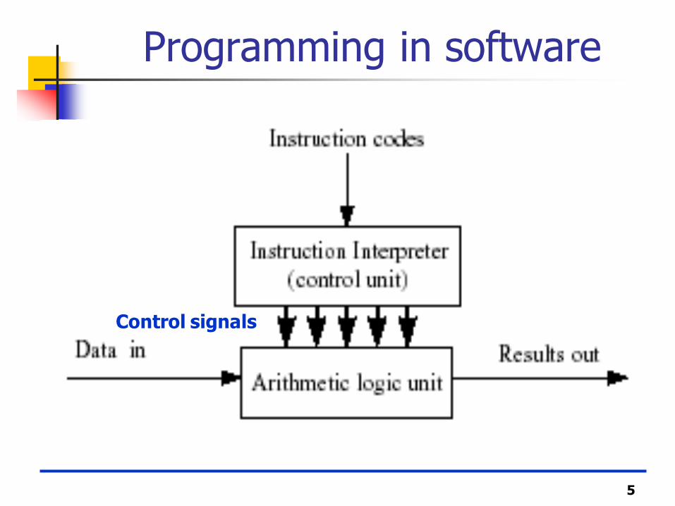
Programming in software
Control signals

6
What is a program?
A sequence of steps
For each step, an arithmetic or logical operation is done
For each operation, a different set of control signals is needed

7
Function of Control Unit
For each operation a unique code is provided
e.g. ADD, MOVE
A hardware segment accepts the code and issues the control signals
We have a computer!

8
Von Neumann architecture
Von Neumann is credited with developing the idea of
controlling the operation of hardware through the
manipulation of control signals
First machines (e.g., ENIAC) had to be physically
rewired to change the computation being performed
Von Neumann used the memory of the computer to
store the sequence of the control signal manipulations
required to perform a task -- software programming
the Von Neumann architecture has been the basis for
virtually all computer designs since the first generation
9
Von Neumann
Stored Program concept
Main memory storing programs and data
ALU operating on binary data
Control unit interpreting instructions from memory and executing
Input and output equipment operated by control unit

10
Structure of Von Neumann machine

11
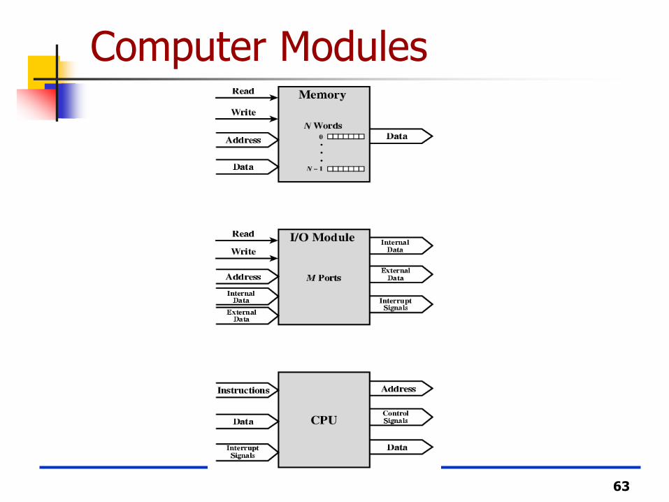
Components
The Control Unit and the Arithmetic and Logic Unit constitute the Central Processing Unit
Data and instructions need to get into the system and results out
Input/output
Temporary storage of code and results is needed
Main memory

12
Computer Components: Top Level View

13
CPU registers
MAR: specifies the address in memory for the next read or write.
MBR: contains the data to be written into memory or receives the data read from memory.
I/OAR : specifies a particular I/O device.
I/O BR: is used for the exchange of data between an I/O module and the CPU.
14
I/O module
An I/O module transfers data from external devices to the CPU and memory, and vice versa. It contains internal buffers for temporarily holding this data until it can be sent on.
15
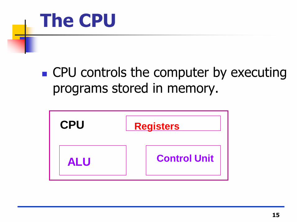
The CPU
CPU controls the computer by executing programs stored in memory.
CPU Registers
Control Unit ALU

16
The CPU
Program is a set of instructions.
An instruction is a bit string →
machine language
The instructions performed by a CPU are its instruction set (unique for each CPU).

17
Memory
Memory of any computer consists of large number of elements, each one can store one bit.
Computers use binary systems → the memory section of a computer contains storage units, which can be constructed from any device capable of storing two values corresponding to 0 and 1.
Storage device must have two stable states, and must have the capability to switch between them.

18
Memory
Until about 1975 the most popular device was the magnetic core (tiny rings of ferromagnetic material).
Since 1975, core technology has been completely replaced by semiconductor memories. The 2 states 0 & 1 are represented by 2 differing voltage levels across a transistor.
19
Memory
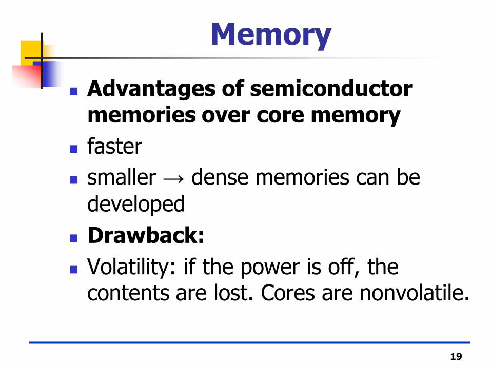
Advantages of semiconductor memories over core memory
faster
smaller → dense memories can be
developed
Drawback:
Volatility: if the power is off, the contents are lost. Cores are nonvolatile.

20
CLASSIFICATION OF MEMORY
• Broadly classified into two : o Primary Memory ( Main Memory ) o Secondary Memory
• Primary memory: is the memory internal to the computer. i.e. the memory generally placed on the Mother board of the computer.
• Secondary memory: is the memory external to the computer. o Generally for large storage of data o Generally for permanent storage of data

21
CLASSIFICATION OF MEMORY
• It can be further divided into two parts: o RAM ( Random Access Memory )
o ROM ( Read Only Memory)
RAM ROM
1. Random Access memory 2. Temporary memory 3. Volatile Memory i.e. contents are
lost when power is switched Off. 4. Read and Write memory
1. Read Only Memory. Memory used to store the startup instructions i.e. Booting instructions.
2. Permanent Memory 3. Non-Volatile memory i.e. contents
are not erased when the power is switched off.
4. Random Access memory
Difference between RAM and ROM

22
Memory
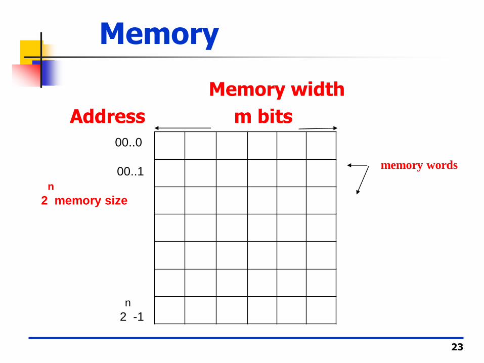
Memory elements are organized into groups (cells) that can store a fixed size of bits.
Each group is assigned a unique number known as its address.
If a memory has k cells, they will have addresses 0 to k-1
If an address has n bits → the maximum number
of cell directly addressable is 2 (address space)
The number of bits in each location is called the memory width = cell size = word size.
n
23
Memory
Memory width
Address m bits
memory words
00..0
00..1
n
2 memory size
n
2 -1

24
Memory Examples
1. Memory unit 2048 X 10 → memory width =10 bits,
address space 2048 = 2
address consists of 11 bits.
2. Memory word size 8-bit → memory width
8 bits.
Address consists of 12 bits →
address space = memory size =2 = 4096
11
12

25
Memory
Usually a group of 8 bits is called a “byte”.
The bytes are the shortest groupings of bits that the computers can handle at a time (fetch and store, read and write)
• 8 bits = 1 byte
• 1024 bytes (210)= 1 Kilo Bytes
• 1024 KB (220)= 1 Mega Byte
• 1024 MB (230)= 1 Giga Byte
26
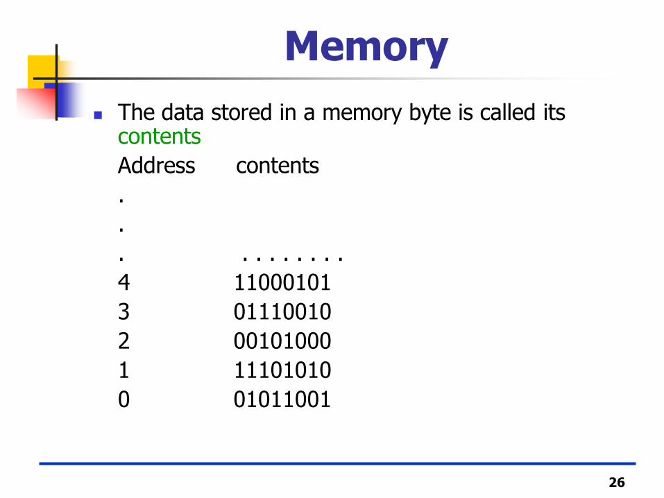
Memory
The data stored in a memory byte is called its contents
Address contents
.
.
. . . . . . . . .
4 11000101
3 01110010
2 00101000
1 11101010
0 01011001

27
Memory
In a typical microcomputer, 2 bytes form a word (16-bit) (some microcomputers 4 bytes (32-bit) → word).
The words have the same bit length as the computer’s data registers, data
buses, and arithmetic unit.
28
Memory
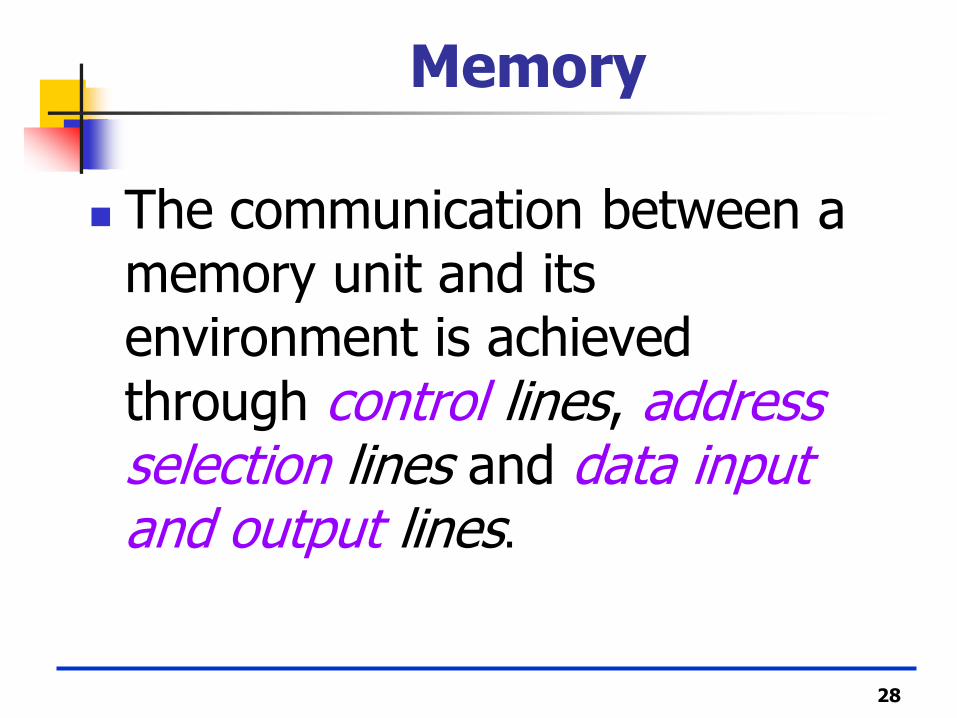
The communication between a memory unit and its environment is achieved through control lines, address selection lines and data input and output lines.

29
Memory
Memory unit
k words = 2n
m bits per word
read
write
n address
Selection
Lines
Control
Signal
m data output lines
m data input lines

30
Memory
The address lines are permanently connected to the output of a single external register called MAR (memory address register).
Binary information is transferred between words of memory and the external environment through a common register MBR (memory buffer register) [other names: data register, information register].
31
Memory
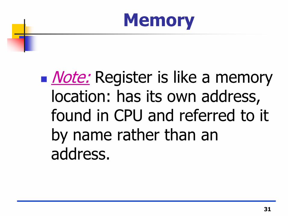
Note: Register is like a memory location: has its own address, found in CPU and referred to it by name rather than an address.

32
Memory
m
Memory Unit
2n x m
MBR
MA R
m bits
data
n bits
address
Read / write
Size of MAR = n
Size of MBR = m

33
Sequence of operations
For Read operation:
Transfer the address bits of the required word into MAR
Activate the Read control signal →
information will be stored in MBR. The original content in the memory location is not changed.

34
Read operation
Word
Control R/W
Select (address) data out
Read: MBR ← M [MAR]
35
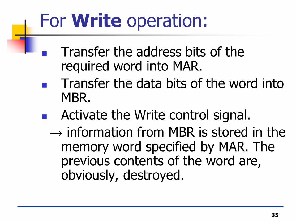
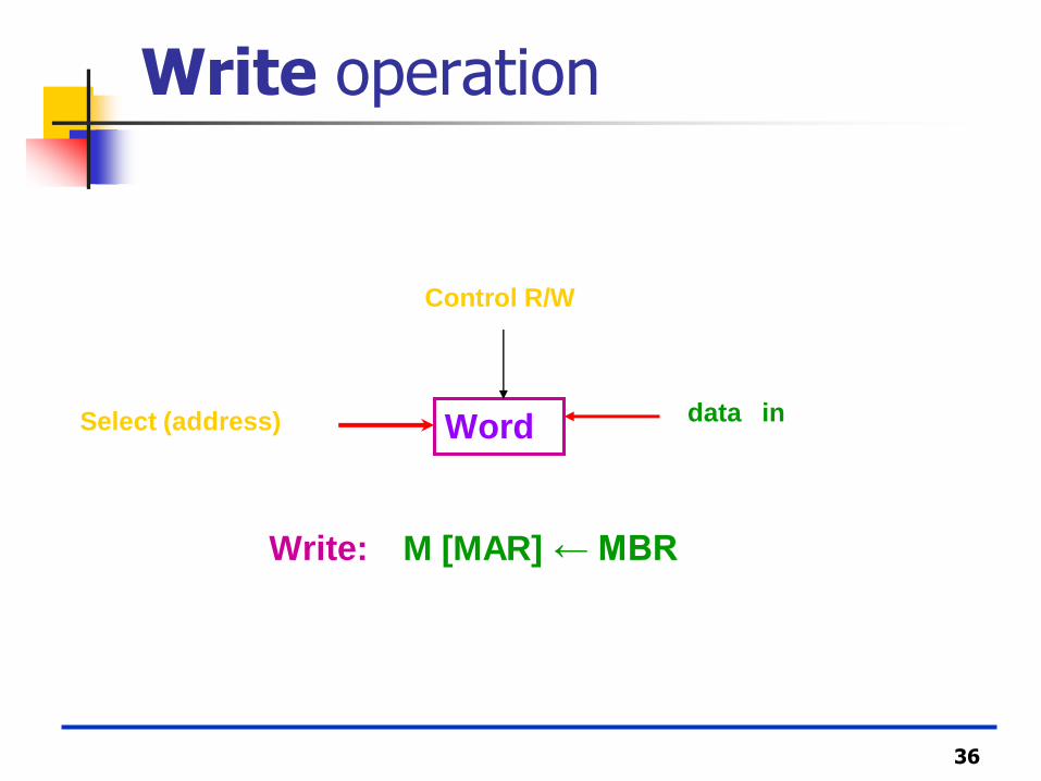
For Write operation:
Transfer the address bits of the required word into MAR.
Transfer the data bits of the word into MBR.
Activate the Write control signal.
→ information from MBR is stored in the memory word specified by MAR. The previous contents of the word are, obviously, destroyed.
36
Write operation
Control R/W
Select (address) Word
Write: M [MAR] ← MBR
data in

37
Example ( 1 )
Given following instruction format which is stored in 1 word
3 bits 7 bits
Opcode address
MAR = 7 bits. → address space = 2 =
128
MBR = 10 bits ( memory word width).
7
38
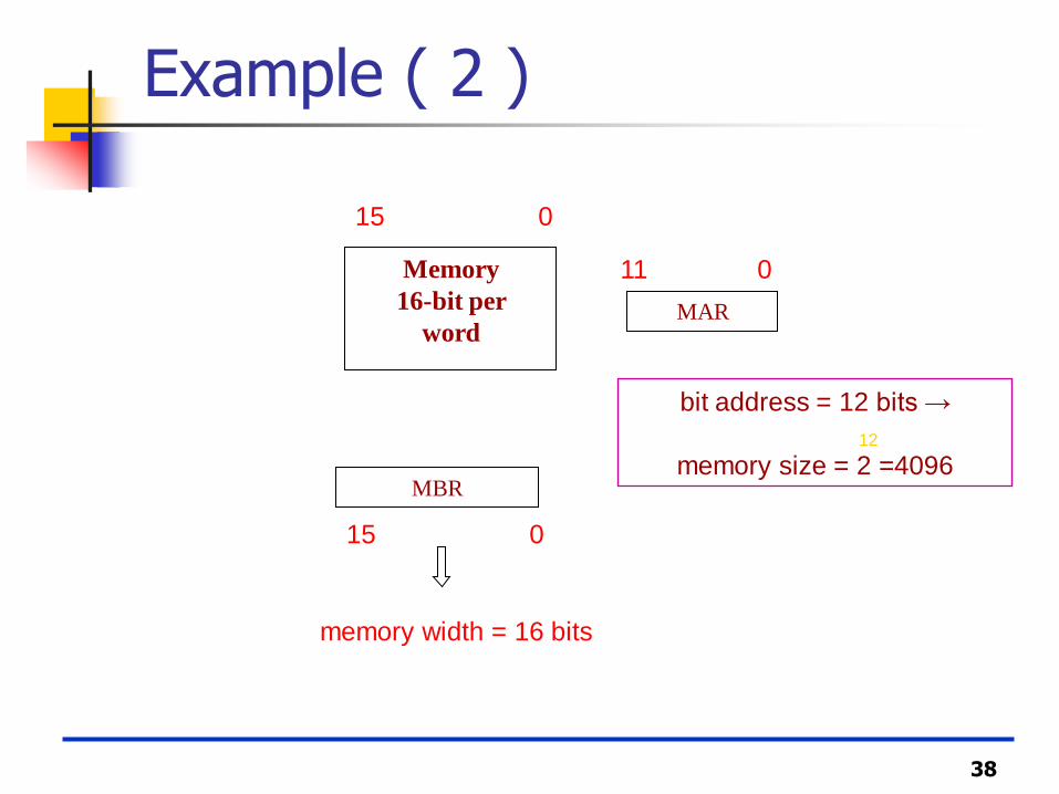
Example ( 2 )
Memory
16-bit per
word
MBR
MAR
15 0
15 0
11 0
bit address = 12 bits →
memory size = 2 =4096
memory width = 16 bits
12

39
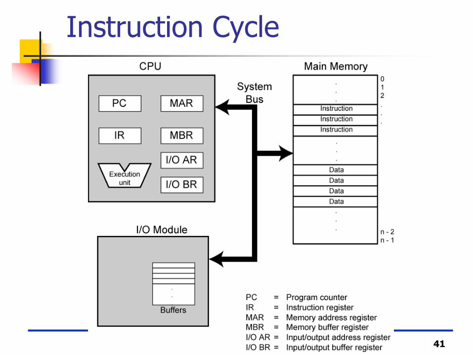
Computer Function
The basic function performed by a
computer is execution of a program,
which consists of a set of instructions
stored in memory.
Instruction processing consists of two
steps: the processor reads (fetches)
instructions from memory one at a time
and executes each instruction.

40
Instruction Cycle
Two steps:
Fetch
Execute
Program execution halts only if the machine is turned off, some sort of unrecoverable error occurs, or a program instruction that halts the computer is encountered.
41
Instruction Cycle

42
Fetch Cycle
Program Counter (PC) holds address of next instruction to fetch
Processor fetches instruction from memory location pointed to by PC
Increment PC
Unless told otherwise
Instruction loaded into Instruction Register (IR)
Processor interprets instruction and performs required actions

43
Execute Cycle
Processor-memory data transfer between CPU and main memory
Processor I/O Data transfer between CPU and I/O module
Data processing Some arithmetic or logical operation on data
Control Alteration of sequence of operations
e.g. jump
Combination of above

44
Characteristics of some Hypothetical Machine
Opcode operands
A machine instruction has two parts: an opcode and operands
Specify the type of
operation immediate data or address
0 3 4 15

45
Characteristics of some Hypothetical Machine
Word size: 16 – bits numbered – (Lsb) 0 through 15 (Msb)
Instruction format: 0 – 3 opcode (4-bits) 16 opcodes
4 – 15 address(12-lines) 212= 4096 words
Integer format: 0 sign bit, 1 – 15 magnitude
Program counter (PC) = address of instruction
Instructions register (IR) = instruction being executed
Accumulator (AC) = temporary storage
0001 (1 Hex) = load AC from memory
0010 (2 Hex) = store AC to memory
0101 (5 Hex) = add to AC from memory

46
Example of Program Execution
1 H= load AC from memory 2 H = store AC to memory 5 H = add to AC from memory

47
Instruction execution
Determine the address of the next instruction
Fetch that instruction from memory
Decode the instruction to determine what is to be
performed
Calculate the addresses of needed operands and
fetch the operands
Perform the operation on the operands
Store the results
Check for and service pending interrupts

48
Instruction Cycle State Diagram

49
Interrupts
Mechanism by which other modules (e.g. I/O) may interrupt normal sequence of processing
Program e.g. overflow, division by zero
Timer Generated by internal processor timer
Used in pre-emptive multi-tasking
I/O from I/O controller
Hardware failure e.g. memory parity error

50
Program Flow Control
51
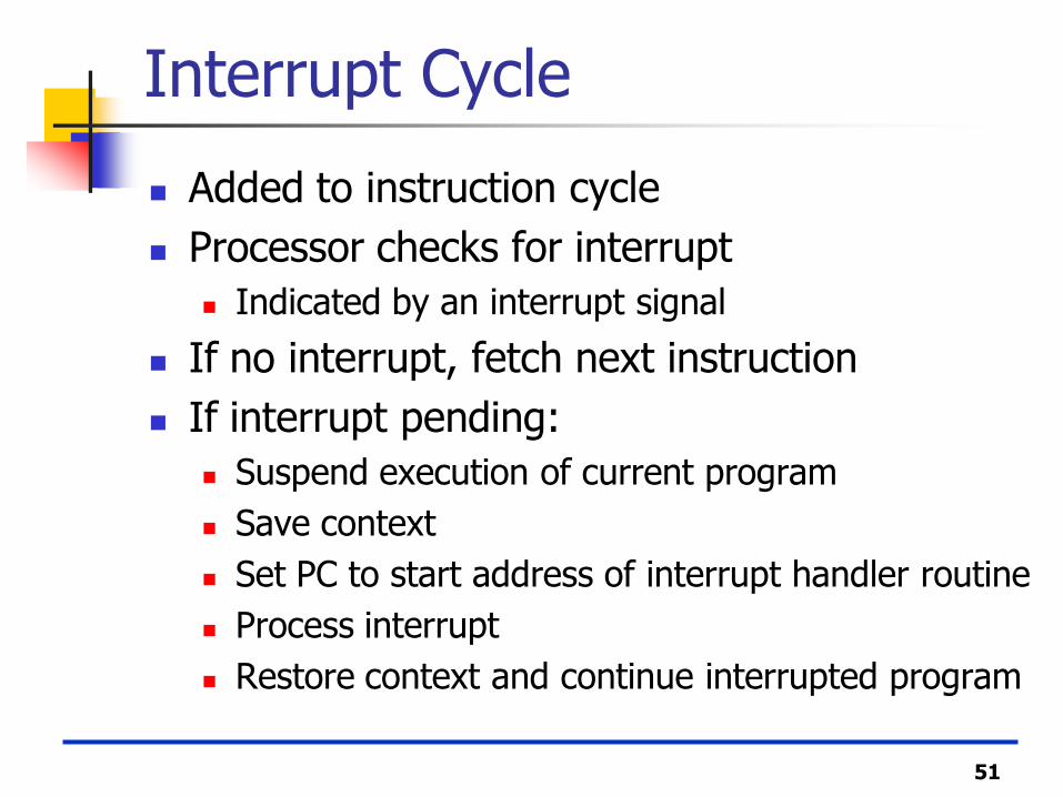
Interrupt Cycle
Added to instruction cycle
Processor checks for interrupt
Indicated by an interrupt signal
If no interrupt, fetch next instruction
If interrupt pending:
Suspend execution of current program
Save context
Set PC to start address of interrupt handler routine
Process interrupt
Restore context and continue interrupted program

52
Transfer of Control via Interrupts

53
Instruction Cycle with Interrupts

54
Program Timing: Short I/O Wait
55
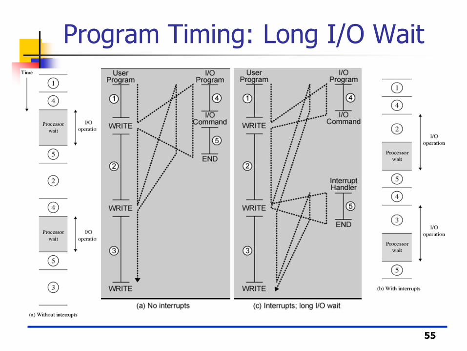
Program Timing: Long I/O Wait
56
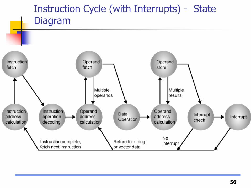
Instruction Cycle (with Interrupts) - State Diagram
57
Multiple Interrupts
Disable interrupts
Processor will ignore further interrupts whilst processing one interrupt
Interrupts remain pending and are checked after first interrupt has been processed
Interrupts handled in sequence as they occur
Define priorities
Low priority interrupts can be interrupted by higher priority interrupts
When higher priority interrupt has been processed, processor returns to previous interrupt

58
Multiple Interrupts - Sequential
59
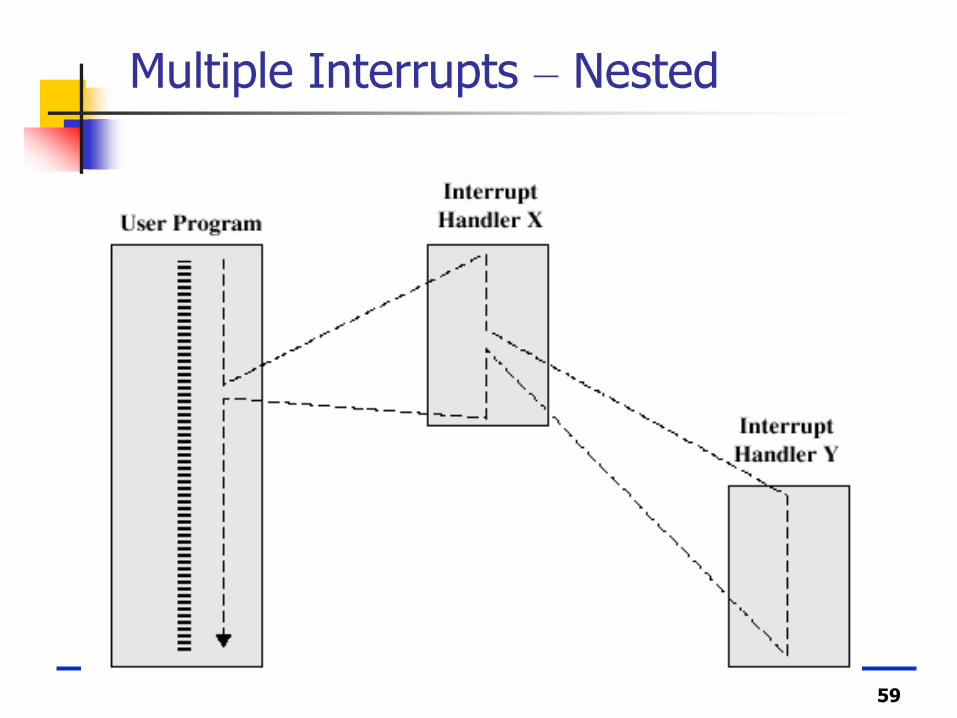
Multiple Interrupts – Nested

60
Time Sequence of Multiple Interrupts
61
I/O Function
An I/O module can exchange data directly with the processor; the processor can read or write data to an I/O module.
In some cases, it is desirable to allow I/O exchanges to occur directly with memory. In such a case, the processor grants to an I/O module the authority to read from or write to memory, so that the I/O-memory transfer can occur without tying up the processor. During such a transfer, the I/O module issues read or write commands to memory, relieving the processor of responsibility for the exchange.This operation is known as
direct memory access (DMA).
62
Connecting
All the units must be connected
Different type of connection for different type of unit
Memory
Input/Output
CPU
63
Computer Modules

64
Memory Connection
Receives and sends data
Receives addresses (of locations)
Receives control signals
Read
Write

65
Input/Output Connection(1) Similar to memory from computer’s viewpoint
Output
Receive data from computer
Send data to peripheral
Input
Receive data from peripheral
Send data to computer

66
Input/Output Connection(2)
Receive control signals from computer
Send control signals to peripherals
e.g. spin disk
Receive addresses from computer
e.g. port number to identify peripheral
Send interrupt signals (control)
67
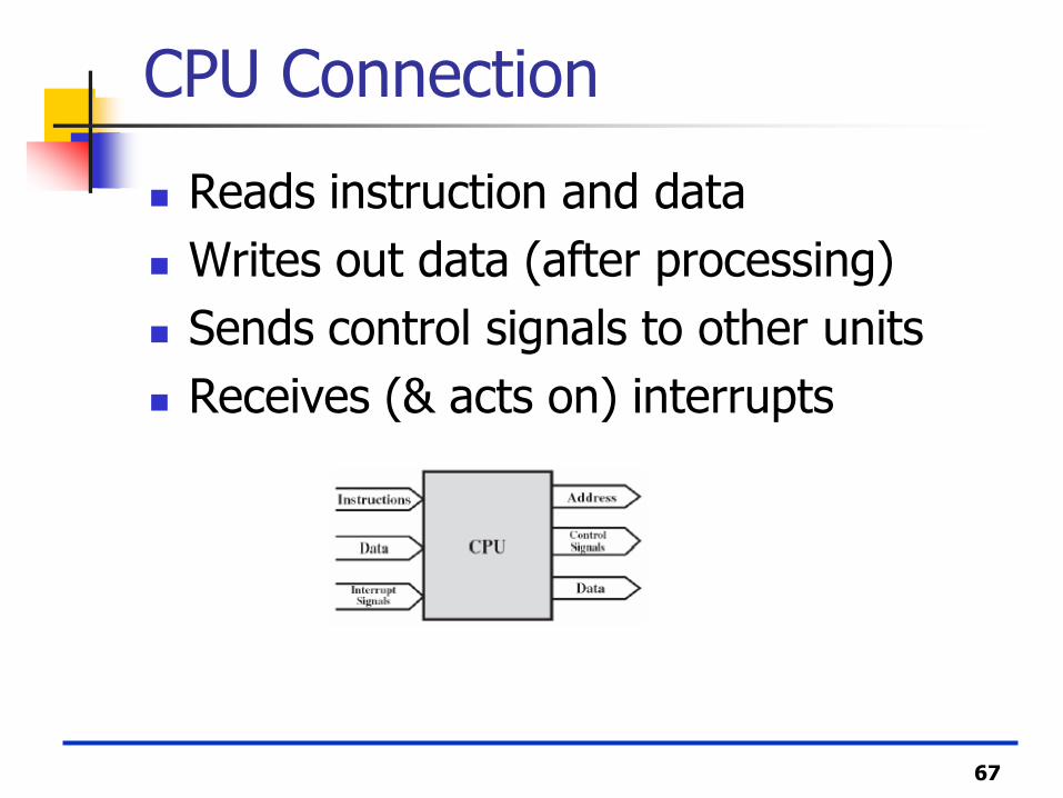
CPU Connection
Reads instruction and data
Writes out data (after processing)
Sends control signals to other units
Receives (& acts on) interrupts
68
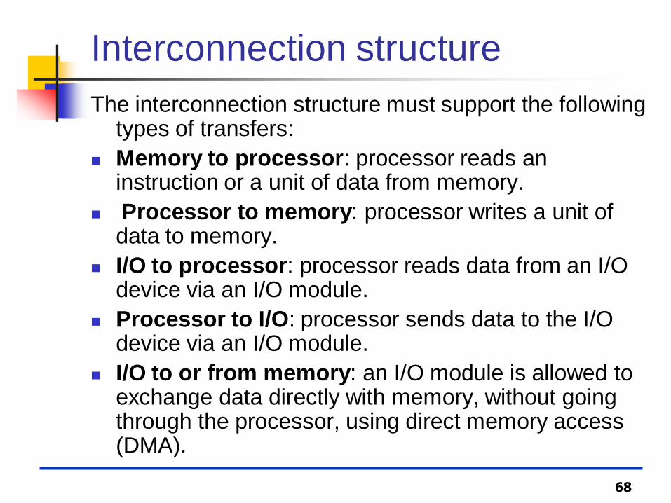
Interconnection structure
The interconnection structure must support the following types of transfers:
Memory to processor: processor reads an instruction or a unit of data from memory.
Processor to memory: processor writes a unit of data to memory.
I/O to processor: processor reads data from an I/O device via an I/O module.
Processor to I/O: processor sends data to the I/O device via an I/O module.
I/O to or from memory: an I/O module is allowed to exchange data directly with memory, without going through the processor, using direct memory access (DMA).

69
Bus Interconnection
A bus is a communication pathway
connecting two or more devices. Multiple
devices can be connected to the same bus at
the same time.
Typically, a bus consists of multiple
communication pathways, or lines. Each line
is capable of transmitting signals representing
binary 1 or binary 0.
A bus that connects major computer
components (processor, memory, I/O) is
called a system bus.

70
Buses
There are a number of possible interconnection systems
Single and multiple BUS structures are most common
e.g. Control/Address/Data bus (PC)
e.g. Unibus (DEC-PDP)
71
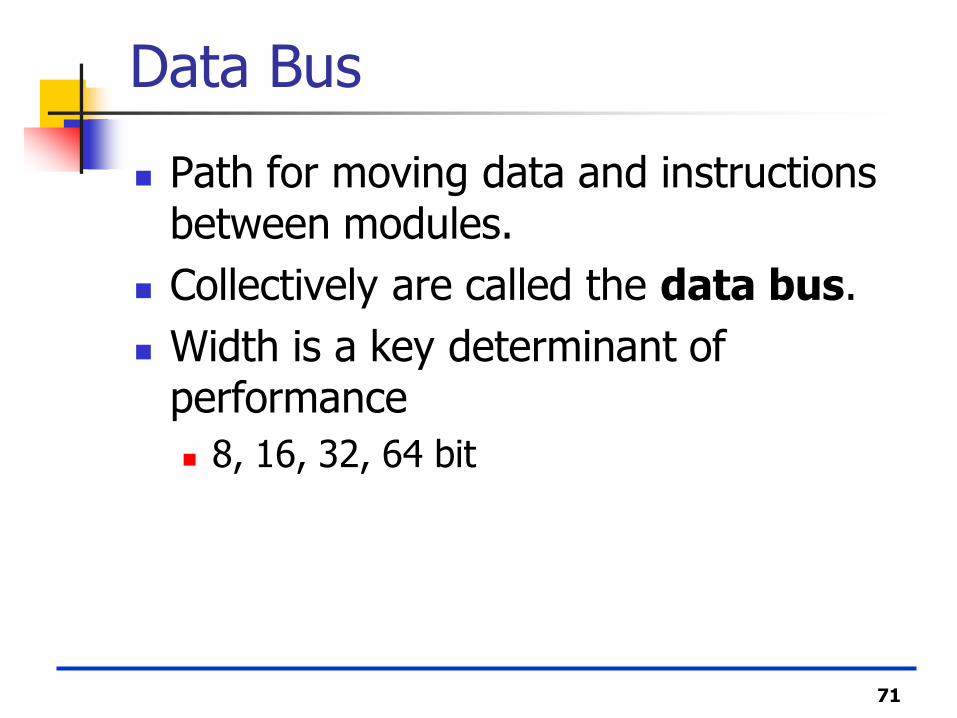
Data Bus
Path for moving data and instructions between modules.
Collectively are called the data bus.
Width is a key determinant of performance
8, 16, 32, 64 bit

72
Address bus
Identify the source or destination of data
e.g. CPU needs to read an instruction (data) from a given location in memory
Bus width determines maximum memory capacity of system
e.g. 8080 has 16 bit address bus giving 64k address space

73
Control Bus
Used to control the access to and the use of the data and address lines.
Control signals transmit command and timing information
Memory read/write signal
Interrupt request
Clock signals
74
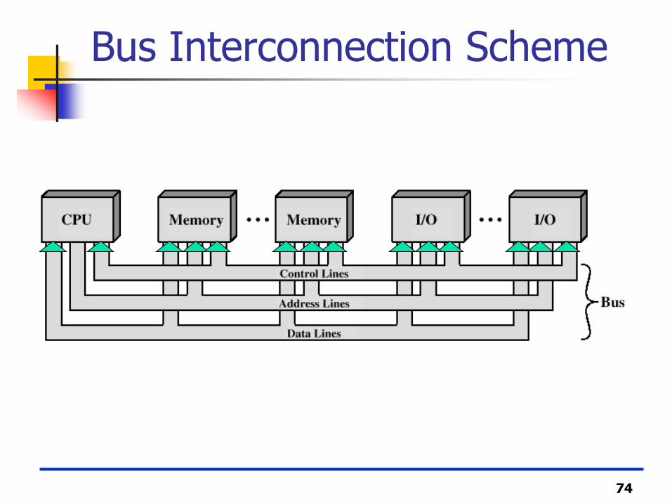
Bus Interconnection Scheme

75
Timing
T0 ensure that the steps of instruction are carried out in an orderly fashion, a clock circuit controls the processor by generating a train of clock pulses
Voltage
Time
76
Timing
The time interval between two pulses is known as a clock period.
The number of pulses per second is called clock rate or clock speed (or frequency), measured in megahertz (MHZ).
1 MHZ = 1 million cycles (pulses) per second.
The computer circuits are activated by the clock pulses → the circuits perform an operation only when a clock pulse is present.

77
Timing
Each step in instruction fetch and execution cycles requires one or more clock period. For example, the 8086 takes 4 clock periods to do a memory read.
If we speed up the clock circuit, a processor can be made to operate faster, but each processor has a rated maximum clock speed beyond which it may not function properly.

Performance Assessment/ Clock Speed
A processor can be driven by a clock with frequency f
Clock cycle time τ = 1/f
CPI is the average cycles per instruction for a program.
Ic instruction count is the number of machine instructions executed for that program until it runs to completion or for some defined time interval.
T time needed for processor to execute a given program:
T= Ic x CPI x τ
78
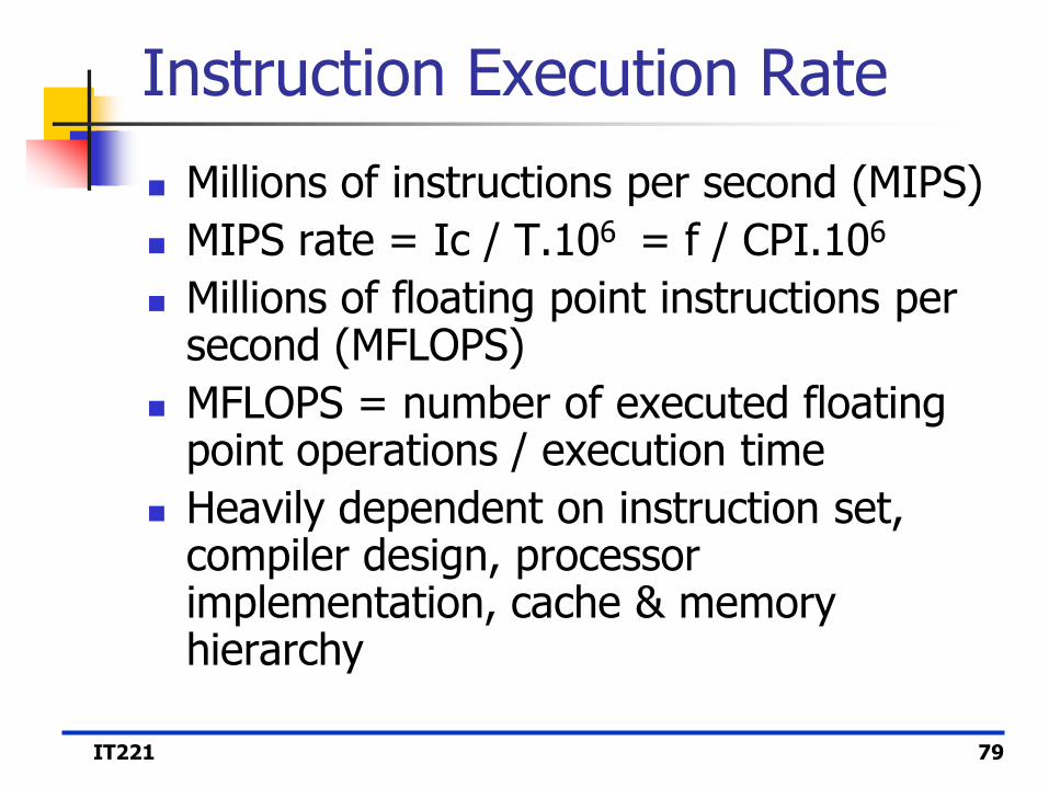
Instruction Execution Rate
Millions of instructions per second (MIPS)
MIPS rate = Ic / T.106 = f / CPI.106
Millions of floating point instructions per second (MFLOPS)
MFLOPS = number of executed floating point operations / execution time
Heavily dependent on instruction set, compiler design, processor implementation, cache & memory hierarchy
IT221 79

80
Op Inst. count
Clock Cycle #
ALU 50 1 .5
Load 20 5 1
Store 10 3 .3
Branch 20 2 .4
CPI =2.2
Total no of instructions = Ic = 100
CPU time (T) = Instruction count x CPI x clock_cycle time
= 100x2.2 x1/1x10^9= 220 nsec.
A 1-GHZ processor was used to execute a program
with the following instruction mix and clock cycle count:
EXAMPLE