component test reference - islandsmt
TRANSCRIPT

Z1800-Series
Component Test Reference
Teradyne, Inc.
Assembly Test/Walnut Creek2625 Shadelands Drive, Walnut Creek, CA 94598-2597Publication Number 1800M247 Copyright Teradyne, Inc.
Product Warranty THE STANDARD TERADYNE WARRANTY CONSTITUTES THE ONLY REPRESENTATION OR WARRANTY MADE BY TERADYNE WITH RESPECT TO ANY EQUIPMENT, GOODS OR SERVICES SUPPLIED BY TERADYNE. TERADYNE MAKES NO OTHER WARRANTIES OR REPRESENTATIONS, EXPRESSED OR IMPLIED, IN FACT OR IN LAW, INCLUDING THE IMPLIED WARRANTIES OF MERCHANTABILITY AND FITNESS FOR A PARTICULAR PURPOSE. IN NO EVENT WILL TERADYNE BE LIABLE FOR INCIDENTAL, SPECIAL OR CONSEQUENTIAL PENALTIES OR DAMAGES, INCLUDING LOST PROFITS, OR PENALTIES AND/OR DAMAGES FOR DELAY IN DELIVERY OR FAILURE TO GIVE NOTICE OF DELAY, EVEN IF TERADYNE HAS BEEN ADVISED OF THE POSSIBILITY OF SUCH DAMAGES.
Due to an ongoing policy of constantly updating equipment and procedures, the contents of this document are subject to change without notice.
Teradyne assumes no responsibility for errors or for any damages that result from the implementation of the procedures described in this publication. Teradyne also reserves the right to make changes in its products without incurring any obligation to incorporate such changes in units previously sold or shipped. Teradyne makes no commitment to update nor to keep current the information contained in this document.
Teradyne assumes no responsibility for the use of any circuitry other than the circuitry embodied as a Teradyne product. No other circuit patent licenses are implied.
This software system consists of computer software and documentation. It contains trade secrets and confidential information which are proprietary to Teradyne, Inc. Its use or disclosure in whole or in part without the express written permission of Teradyne, Inc. is prohibited.
This software system is also an unpublished work protected under the copyright laws of the United States of America. If this work becomes published, the following notice shall apply:
Copyright © 1994, 1995, 1996, 1997, 1998, Teradyne, Inc. All Rights Reserved
Trademarks The following are trademarks or registered trademarks of Teradyne and may be used to describe only Teradyne, Inc., Assembly Test/Walnut Creek products:
Teradyne documentation contains references to Borland and Paradox which are trademarks of Borland International, Inc. CodeView, Microsoft, MS-DOS, QuickC, and Windows are either registered trademarks or trademarks of Microsoft in the United States and/or other countries. Codewright is a trademark of Premia Corporation. ETHERNET is a trademark of Xerox Corporation. IBM, MicroChannel and PS/2 are registered trademarks of International Business Machines, Inc. LabWindows,
NI-488.2 and NI-VXI are trademarks of National Instruments Corporation. MobyTurbo and ZMODEM-90 are trademarks of Omen Technology, Inc. QEMM is a trademark of Quarterdeck Office Systems, Inc.
Additional copies of this manual may be obtained from
Teradyne, Inc.Assembly Test/Walnut Creek2625 Shadelands DriveWalnut Creek, CA 94598925.932.6900 TWX 910.385.6300
Z850 Z1820 Boundary Scan Intelligent Diagnostics (BSID)
Z850F/I Z1840 and Z1840M DeltaScan
Z860 Z1840VP® Digital Function Processor (DFP)
Z875 Z1850 and Z1850M FrameScan
Z8000 Z1850VP® HostLink
Z8500 Z1860 and Z1860M MultiScan
Z1800 Z1860VP® ProcessWatch
Z1803 and Z1803 Plus Z1866 Programmer Efficiency Package (PEP)
Z1805 Z1880 Safecracker
Z1808 Z1884 Test Toolbox
Z1811 Z1888 Tester-Aided Instruction
Z1811VP Z1890 TestQA
Z1812 APC WaveScan
Z1812VP AutoLoad
Z1800-SERIES COMPONENT TEST REFERENCE
Manual History First Edition, October 1998, F.2b System Software
Publications No. 1800M247© 1998 Teradyne, Inc., Assembly Test/Walnut Creek2625 Shadelands Drive • Walnut Creek, CA 94598 • (925) 932-6900Customer Service Hotline (800) 457-8326

v
CONTENTS
Preface vii
1 Shorthand and Longhand TestingPRISM-Z.......................................................................................................... 1-1Shorthand Tests .............................................................................................. 1-1Longhand Tests............................................................................................... 1-1
Test V ............................................................................................................. 1-2TEST V STIM V ............................................................................................. 1-5Test V Stim I .................................................................................................. 1-7Test I Stim V ................................................................................................ 1-10Dual Stimulus Modes .................................................................................. 1-11
2 Board PowerStep Worksheet ............................................................................................... 2-1
Editing Test Properties .................................................................................. 2-5
3 CapacitorsCapacitor Theory ............................................................................................. 3-2
Capacitor Range and Accuracy ..................................................................... 3-3Step Worksheet Editing ................................................................................... 3-4
Component Properties .................................................................................. 3-5Test Properties .............................................................................................. 3-5
Extended Shorthand Test Mode...................................................................... 3-6Test Parameters ............................................................................................ 3-7Worksheet Editing ......................................................................................... 3-8
Cap Phase Test Type...................................................................................... 3-8EAA Specifications ........................................................................................ 3-9Theory ......................................................................................................... 3-12Cap Phase for Capacitor and RC Tests ....................................................... 3-13
Extended Analog Assembly Specs................................................................ 3-16Resistor/Capacitor Testing ............................................................................ 3-17
Specifications .............................................................................................. 3-20Residual Charges in Large Capacitors ........................................................ 3-20Longhand Capacitor Tests ........................................................................... 3-21
4 Digital DevicesGray Code and Vector Overview..................................................................... 4-1
Digital Test Specifications .............................................................................. 4-1Gray Code Tests ............................................................................................. 4-3
Specifications ................................................................................................ 4-3Gray Code Stimulus ...................................................................................... 4-4Gray Code Measurement .............................................................................. 4-8Using Gray Code to Test Memory Devices .................................................. 4-10
Vector Tests .................................................................................................. 4-11Specifications .............................................................................................. 4-11Vector Test Methods .................................................................................... 4-12
Digital Test Editing......................................................................................... 4-15Gray Code Test Properties .......................................................................... 4-16Vector Test Properties ................................................................................. 4-21
Mixed Mode Tests ......................................................................................... 4-32Gray Code ................................................................................................... 4-32Vector Tests ................................................................................................. 4-38
Spectrum 8800-Series Test Development Reference
vi
5 Diodes and ZenersTesting Diodes & Zeners ................................................................................. 5-2
Range and Accuracy ..................................................................................... 5-3Step Worksheet Editing ................................................................................. 5-3
6 DischargeDischarge Testing............................................................................................ 6-1
Editing ........................................................................................................... 6-1Adding Discharge Test Step for Global APC ................................................. 6-3
7 InductorsRange and Accuracy ....................................................................................... 7-1Step Worksheet Editing ................................................................................... 7-1
Component Properties Editing ...................................................................... 7-2
8 InterconnectsContinuities Tests and Editing ......................................................................... 8-1
Component Properties Editing ...................................................................... 8-1Test Properties Editing .................................................................................. 8-2
Ignores Testing................................................................................................ 8-3Jumpers Testing .............................................................................................. 8-3Merge_SC (Merge Special Case) Testing....................................................... 8-4Shorts Tests and Editing ................................................................................. 8-4Opens Testing ................................................................................................. 8-4
9 Linear AnalogEditing.............................................................................................................. 9-1
Test Properties Editing .................................................................................. 9-2
10 Power-Off Longhand Analog
11 Potentiometers and RheostatsTest Step Editing ........................................................................................... 11-2
Component Properties ................................................................................ 11-2Test Properties ............................................................................................ 11-2
12 ResistorsStandard Resistor Test (Extended Off) ......................................................... 12-1
Theory ......................................................................................................... 12-1Resistor Test Step Editing ........................................................................... 12-2
Standard Resistor Test (Extended On) ......................................................... 12-5Extended Shorthand Test Editing ................................................................ 12-5
Resistors in Parallel with other Components................................................. 12-6Longhand Testing of Resistors...................................................................... 12-6
13 RpacksRpack Test Step Editing ................................................................................ 13-1
14 Transistor and GainTesting Techniques ....................................................................................... 14-1
Field Effect Transistors ................................................................................ 14-2Reversed Transistors and Beta Test ............................................................ 14-2
Transistor Test Step Editing .......................................................................... 14-3Component Properties Editing .................................................................... 14-3Test Properties Editing ................................................................................ 14-4

an
nge and
AM
and
PREFACE
This document is an alphabetical reference of analog and digital device tests. It starts withexplanation of shorthand and longhand test methods.
The analog component chapters cover shorthand and longhand test methods, test types, raaccuracy specifications, calculating test accuracy, and test step editing.
The digital section covers test techniques for SSI/MSI, non-programmable LSI, ROM and Rdevices, and ASICs and PALs, with the following subject areas:
• Test Philosophy
• Test Specifications
• Gray-Code Test Methods
• Vector Test Methods
• Digital Test Editing
Refer to the Z1800-Series Programmer’s Guidebook , Chapter 12, for vector test strategies.
The table below describes the unit multipliers or scales that appear often in this reference throughout the software.
Multiplier Unit Example X Multiplier
U (micro) V (Volt) UV 10-6
M (milli) V (Volt) MV 10-3
K (kilo) O (Ohm) KO 103
M (mega) O (Ohm) MO 106
N (nano) A (Ampere) NA 10-9
U (micro) A (Ampere) UA 10-6
M (milli) A (Ampere) MA 10-3
U (micro) H (Henry) UH 10-6
M (milli) H (Henry) MH 10-3
P (pico) F (Farad) PF 10-12
N (nano) F (Farad) NF 10-9
U (micro) F (Farad) UF 10-6
M (milli) F (Farad) MF 10-3
M (milli) S (seconds) MS 10-3

hand.
to test nu
es mal
alog design ption
as
ons of
-Z
Z
ers are
d and
t
eneric ile the ATB.
of
1 SHORTHAND AND LONGHAND TESTING
The test system can take analog measurements in two distinct modes: shorthand and long
Common to both shorthand and longhand tests is the ability to apply six decimal precision limits such as Value, High and Low. When you select Scale in the worksheet, a pop-up meappears where you select the scale and either Default or 6 decimal precision. All existing programs have Default selected, which is the backwards compatible mode. In Default, valugreater than or equal to 100.0 have two decimal precision; all other values have three deciprecision.
PRISM-Z The PRISM-Z (PRecision Integrated Signal Measurement) module is a next generation anmeasurement subsystem for in-circuit testers. It is a Digital Signal Processor-based (DSP) that accurately measures values and circuit configuration. The PRISM-Z instrument is an ofor Z1800-Series systems.
Systems that include the PRISM-Z option retain the ATB (Analog Test Board) in order to guarantee backward compatibility with existing programs as well as for ordinary tasks suchshorts, continuities, and Node Finder. You can mix and match PRISM-Z and ATB tests throughout your test program. The following test types are available on F.2a and later versi18xx system software:
• Capacitor
• Inductor
• Resistor
• Test I Stim V
• Test V
• Test V Stim I
• Test V Stim V
You can convert existing component tests that use ATB worksheets to tests that use PRISMworksheets. You can also convert PRISM-Z worksheets back to ATB.
Refer to the Z1800-Series PRISM-Z User’s Guide for a complete discussion about the PRISM-test types available for longhand and shorthand tests.
Shorthand Tests Shorthand test modes are geared toward specific component tests. In such tests, parametexpressed in the components’ native units (i.e., Ohms for resistors), and compensation is automatically made for parasitic system components and errors before a result is displayecompared to the test limits.
Refer to specific components, such as Capacitor, Resistor, Transistor, for information aboushorthand testing.
Longhand Tests Longhand tests, on the other hand, are more generic. Parameters must be expressed in gunits of volts and amperes, and parasitic system components are not compensated for. Whshorthand test mode is simple to use, longhand gives more control over the features of theHowever, the longhand mode makes programming more complex and is prone to yielding erroneous results. For success in longhand tests, you need to have a solid understanding operation-amplifier theory.
1-2 S
HORTHAND
AND
L
ONGHAND
T
ESTING
ram.
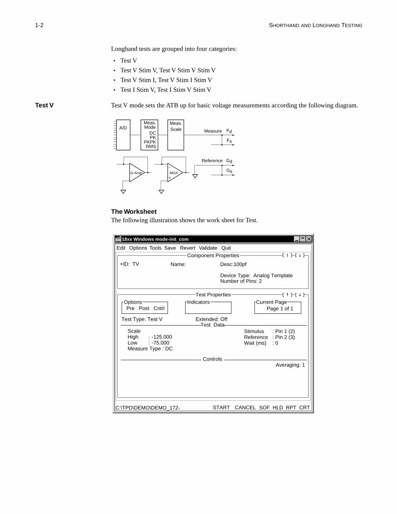
Longhand tests are grouped into four categories:
• Test V
• Test V Stim V, Test V Stim V Stim V
• Test V Stim I, Test V Stim I Stim V
• Test I Stim V, Test I Stim V Stim V
Test V Test V mode sets the ATB up for basic voltage measurements according the following diag
The WorksheetThe following illustration shows the work sheet for Test.
Meas.Scale
Meas.Mode
DCPK
PKPKRMS
A/D
+
-MOA
Measure
Reference
Fd
Fs
Gd
GsG-Amp
Page 1 of 1
18xx Windows mode-init_com
Test Data
Controls
Edit Options Tools Revert Validate Quit
C:\TPD\DEMO\DEMO_172-
Save
Component Properties
Test Properties Options Indicators
Pre Post CntrlCurrent Page
START CANCEL SOF HLD RPT CRT
Page 1 of 1
Averaging: 1
ScaleHighLow -75.000 Measure Type : DC
-125.000StimulusReferenceWait (ms)
::
:::
Pin 1 (2)Pin 2 (3)0
Test Type: Test V Extended: Off
+ID: TV Name: Desc:100pf
Device Type: Analog TemplateNumber of Pins: 2

1-3
S as
ely d after .
closed. nd
ait h g the 0 Hz.
stable RMS
This renced
nd +5 ed as ut the ver
Measure Modes . Test V can be done in four measure modes, DC, Peak, Peak-Peak and RMcontrolled by the measure type field.
Wait Time . The Wait time field is used to specify the time between when the ATB is completset up and when the measurement is taken. An internal relay settling time of 3 ms is applieall relays on the ATB and driver/receiver card have closed and before the wait time applies
For PK, PK–PK, and RMS measurements, the wait time is effectively the gate time for the detectors. For DC measurements it acts simply as a further delay after all the relays have Minimum wait times are enforced depending on the measure type: they are 10 ms for PK aPK–PK, 500 ms for RMS, and 2 ms for DC. The wait time appearing on the Test Propertiesportion of the Step Worksheet is added to these defaults.
The effect of extending wait time depends on the measure type. For PK and PK–PK, the wtime should be at least one full cycle of the signal to be measured. Extending the time mucbeyond that only worsens the risk of capturing possible noise spikes and therefore distortinreading. The 10 ms default for PK and PK–PK allows for signal measurements down to 10Beyond that, extra wait times have to be programmed in Test Properties.
For RMS, the longer one lets the RMS converter collect input signals, the more precise andthe result is. The minimum conversion time the RMS converter needs is 500 ms; therefore,measurements have a much larger default.
Differential Measurements . As you can see from the ATB Setup for Test V Mode diagram above, the reference for the measurement is connected to the system ground via the ATB.causes a problem when the board is powered, since the DUT power supplies are also refeto the same system ground. (The ATB is not floating.)
For example, if on a powered board you want to measure two points that are at + 3 volts avolts in respect to system ground and board-under-test ground, where the +3 V point is usthe reference point, the ATB would connect this point to system ground as well and shorts o+3 volts. To overcome this problem, the system performs differential measurements whene
Test Data for Test V /Test Properties Portion of Step Worksheet
Test V Type:
Scale Measurement-related modifier—uv, mv, V
High Upper limit for a passing measurement. Range = -1000 to +1000
Low Lower limit for a passing measurement. Range =-1000 to +1000
Measure Type DC, Peak, RMS, or Pk-Pk (peak to peak)
Measure Pin/node number(s) at which measurement is taken. 5 nodes max.
Reference Pin/node number(s) of the ground reference (s). 10 nodes max.
Wait (ms) 0 to 65534 ms. Added to default wait of 3 ms typical.
DC DC voltage
Peak Absolute value of greatest excursion from zero in either direction
Peak–Peak Difference between the most positive and most negative excursion
RMS The Root Mean Square average of the measured signal. For a sine wave it equals 0.707 times the peak value
Z1800-Series Component Test Reference

1-4 S
HORTHAND
AND
L
ONGHAND
T
ESTING
and (2)
ARS t by
in the ground rement
ing an
the board under test is powered up by taking two measurements on (1) the reference point the measure point and then subtracting one from the other for the result. Differential measurements therefore take twice the time a single measurement would take.
Differential measurements require that you specify a ground reference node in the PRGMVGround Reference Node field. The system indicates that it took a differential measuremenputting a D in the display line just before the result.
Be aware that differential measurements can be suppressed by listing known ground pointsprogram Header. When a Test V test is executed, and the reference node matches a knownreference node out of the program Header, the system can perform a single-ended measuinstead. Also, if no reference node is specified in Test Properties, no conflict exists and a single-ended measurement is taken by default.
Test V and RangesTest V by default autoranges to higher scales until all ranges are exhausted before displayoverrange flag.
18xx Windows mode-init_com
Page 1 of 1
Test Data
Controls
Edit Options Tools Revert Validate QuitSave
Component ID
Worksheet Options Indicators
Pre Post CntrlCurrent Page
START CANCEL SOF HLD RPT CRTF:\TPD\DIFFV-ICT
Wire Mode: 3 Precise: Off Highguard: Off Averaging: 1Fast Mode: Off
High: 26.4000 Measure: D 24.028 Low: 21.6000 18 Pins: 1 PASS
ScaleHighLowMeasure Type : DC
V26.40021.600
MeasureReferenceWait (ms)
:::
:::
Pin 1 (18)Pin 2 (26)0
Extended: OffTest Type: Test V
+ID: 1 Volt Name: Desc:
Device Type : Power BusNumber of Pins: 2
Value: 24Tol: 10
1-5
ulus.
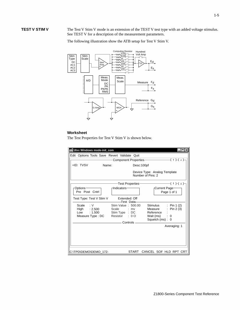
TEST V STIM V The Test V Stim V mode is an extension of the TEST V test type with an added voltage stimSee TEST V for a description of the measurement parameters.
The following illustration show the ATB setup for Test V Stim V.
WorksheetThe Test Properties for Test V Stim V is shown below.
StimType
+
-StimAmp
Ed
Es
K159.935R82K1699.935R89K251KR84K2610KR91K35100KR86K361MR92K4510MR87K55
Computing Resistor
DCAC1AC2AC3
StimScale
*10
DUT
Hundred Volt Amp
Meas.Scale
Meas.Mode
DCPK
PKPKRMS
A/D
+
-MOA
Measure
Reference
Fd
Fs
Gd
GsG-Amp
Page 1 of 1
18xx Windows mode-init_com
Test Data
Controls
Edit Options Tools Revert Validate Quit
C:\TPD\DEMO\DEMO_172-
Save
Component Properties
Test Properties Options Indicators
Pre Post CntrlCurrent Page
START CANCEL SOF HLD RPT CRT
Page 1 of 1
Averaging: 1
ScaleHighLow 1.500 Measure Type : DC
2.500StimulusMeasureReferenceWait (ms)Squelch (ms)
:::
:::::
Pin 1 (2)Pin 2 (3)
00
Test Type: Test V Stim V Extended: Off
+ID: TVSV Name: Desc:100pf
Device Type: Analog TemplateNumber of Pins: 2
V Stim ValueScaleStim TypeResistor
::::
500.00mvDC0 O
Z1800-Series Component Test Reference

1-6 S
HORTHAND
AND
L
ONGHAND
T
ESTING
s
e face.
the
r 0
r the
takes he eld in ment to
In addition to the Test V test type this test setup provides a voltage stimulus via the stimulupoles.
Stimulus magnitude and type . The Stim Value and Scale fields in Test Properties define themagnitude of the stimulus. The Stim Type selects:
• DC or AC sine wave stimulus
Where AC1 equals 159 Hz, AC2 equals 1.59 Khz, and AC3 equals 15.9 Khz.
• Ext
Where Ext stands for external oscillator. The input for this stim source can come from thconnector J4 pin 8 on the front edge of the ATB and the EXT OSC pin in the fixture inter
Stimulus impedance . The Resistor field in Test Properties controls the output impedance ofStimulus circuit when stimulus voltages below 10 V are requested.
Stimulus greater than 10V . When a stimulus greater than 10 V is requested, the *10 amplifie(hundred volt amplifier) is switched into the stimulus path, and the resistor should be set toOhms, otherwise the resulting stimulus can be less than expected. There is no equivalent Stimulus resistor for 100 V option.
Stimulus current limit . The maximum current the stimulus amplifier can deliver is ~275 ma unless limited by a stimulus resistor. When the *10 amplifier is in effect, the minimum guaranteed output current is ~20 ma for DC and ~10 ma for AC stimulus. However, the maximum output current could be as high as 50 ma, depending on ambient temperature orevision of the ATB.
Squelch . Squelch is a means to establish a known initial condition before the measurementplace. It executes after all the relays involved close and before the stimulus is turned on. Tsystem provides a minimum of 3 ms of squelch time that can be extended by the squelch fiTest Properties. Squelch can be used to discharge capacitors associated with the measurebe taken.
Test Data for Test V Stim V /Test Properties Portion of the Step Worksheet
Test V Stim V Type:
Scale Measurement-related modifier—uv, mv, V
High Upper limit for a passing measurement. Range = -1000 to +1000
Low Lower limit for a passing measurement. Range =-1000 to +1000
Measure Type DC, Peak, RMS, or Pk-Pk (peak to peak)
Stim Value Value of stimulus. Range =-1000 to +1000
Scale Stimulus-related modifier—mv, V
Stim Type DC, AC1, AC2, AC3, Ext
Stimulus Pin/node numbers(s) to which stimulus applied. 5 nodes max.
Measure Pin/node number(s) at which measurement is taken. 5 nodes max.
Reference Pin/node number(s) of the ground reference (s). 10 nodes max.
Wait (ms) 0 to 65534 ms. Added to default wait of 3 ms typical.
Squelch (ms) 0 to 65534 ms. Repeatable initial condition to remove stored energy.

1-7
TVSV RangesTest V Stim V by default autoranges to higher scales until all ranges are exhausted before displaying an overrange flag.
Refer to the Z1800-Series Programmer’s Guidebook , Chapter 5, for more information about Test V, Test V Stim V Stim V tests.
Test V Stim I Test V Stim I measures the resulting voltage across a device under test while forcing a programmed current through it.
The following illustration shows the ATB Setup for Test V Stim I 3 Wire Precise off.
StimType
+
-StimAmp
Ed
Es
K159.935R82K1699.935R89K251KR84K2610KR91K35100KR86K361MR92K4510MR87K55
Computing Resistor
DCAC1AC2AC3
StimScale
Meas.Scale
Meas.Mode
DCPK
PKPKRMS
A/D
+
-MOA
Fs
Fd
Gd
Gs
G-Amp
*10
Hundred Volt Amp
Rg
Rg
DUT
Z1800-Series Component Test Reference

1-8 S
HORTHAND
AND
LONGHAND TESTING
low.
The WorksheetThe Test Properties for Test V Stim I is shown below.
Test Properties fields specific to the Test V Stim I Test Type are summarized in the table be
Test Data for Test V Stim I /Test Properties Portion of the Step Worksheet
Test V Stim I Type: Description
Scale Measurement-related modifier—uv, mv, V
High Upper limit for a passing measurement. Range = -1000 to +1000
Low Lower limit for a passing measurement. Range =-1000 to +1000
Measure Type DC, Peak, RMS, or Pk-Pk (peak to peak)
Stim Value Value of stimulus. Range =-1000 to +1000
Scale Stimulus-related modifier—na, ua, ma.
Stim Type DC, AC1, AC2, AC3, Ext
Stimulus Pin/node numbers(s) to which stimulus applied. 5 nodes max.
Measure Pin/node number(s) at which measurement is taken. 5 nodes max.
Reference Pin/node number(s) of the ground reference (s). 10 nodes max.
Wait (ms) 0 to 65534 ms. Added to default wait of 3 ms typical.
Squelch (ms) 0 to 65534 ms. Repeatable initial condition to remove stored energy.
Page 1 of 1
18xx Windows mode-init_com
Test Data
Controls
Edit Options Tools Revert Validate Quit
C:\TPD\DEMO\DEMO_172-
Save
Component Properties
Test Properties Options Indicators
Pre Post CntrlCurrent Page
START CANCEL SOF HLD RPT CRT
Page 1 of 1
Precise: Off Higuard: Off Averaging: 1
ScaleHighLow 1.5 Measure Type : DC
2.5StimulusMeasureReferenceWait (ms)Squelch (ms)
:::
:::::
Pin 1 (2)Pin 2 (3)
00
Test Type: Test V Stim I Extended: Off
+ID: TVSI Name: Desc:100pf
Device Type: Analog TemplateNumber of Pins: 2
V Stim ValueScaleStim Type
:::
500maDC
Wire Mode: 3Guard Mode: Active

1-9
UT e
forced
taken
types.
plifier a as
oise
test. igher T is
um
sures
The ATB is set up to use an inverting operation amplifier to provide Test V Stim I with the Din its feed back path. The stimulus amplifier and computing resistor are used to produce thprogrammed current.
Refer to the Z1800-Series Programmer’s Guidebook , Chapter 5, for an explanation of the op amp theory.
Since the setup uses an inverting op amp, the resulting voltage has the opposite sign of thecurrent. For example, setting up for an +1 ma current through a DUT of 1 KΩ results in a measured voltage of -1V. This holds true only for DC measurements since measurements with PK, PK–PK and RMS are unsigned by nature.
When programming in this mode, take care to use compatible stimulus and measurement For example, an AC stimulus cannot be measured with a DC measure type.
Hundred Volt AmplifierWhen measurements of more than +10 V or less than -12 V are requested, the times 10 amis switched into the circuit, and the maximum current it can deliver is in the area of 10–20 mopposed to ~275 ma without it.
Test V Stim I over Test I Stim V—Advantages/DisadvantagesAdvantage . The Test V Stim I mode is preferable for capacitor testing since it suppresses nand instability due to the placement of the capacitor under test in the feedback.
Disadvantage . The voltage across the DUT is affected by the value of the component underIf the impedance of the DUT is higher than expected, the voltage across the DUT is also hand might cause unguarded paths to affect the result. The worst case occurs when the DUentirely missing, and the MOA output swings all the way to its power supply rail, thereforeputting ±13 V on the board under test. When the 100-volt amplifier is in the circuit, the maximvoltage is about 60 V.
Test V Stim I RangesTest V Stim I does not autorange. An overrange flag is displayed, and the test fails for meaoutside of the current range.
Refer to the Z1800-Series Programmer’s Guidebook , Chapters 3 and 5, for more information about the Test Properties Controls section.
See also Test V, Test V Stim V, and Test V Stim I Stim V in this chapter.
Z1800-Series Component Test Reference

1-10 SHORTHAND AND LONGHAND TESTING
in ough
Test I Stim V The Test I Stim V mode is the opposite of Test V Stim I. In this situation, the DUT is placedthe input leg of the MOA. While the voltage across the DUT is programmed, the current thrit is measured.
The following illustration shows the Test I Stim V 3-Wire Precise Off.
The Test I Stim V Test Properties portion of the Step Worksheet is shown below.
StimType
+
-MOA
+
-Stim
Guard-
+
Fd
Fs
Gd
Gs
Ed
Es
K159.935R82K1699.935R89K251KR84K2610KR91K35100KR86K361MR92K4510MR87K55
Computing Resistor
MeasScale
MeasType
MeasA/D
DCAC1AC2AC3
StimScale
*10
Hundred Volt Amp
Rg
Rg
DUT
Page 1 of 1
18xx Windows mode-init_com
Test Data
Controls
Edit Options Tools Revert Validate Quit
C:\TPD\DEMO\DEMO_172-
Save
Component Properties
Test Properties Options Indicators
Pre Post CntrlCurrent Page
START CANCEL SOF HLD RPT CRT
Page 1 of 1
Precise: Off Higuard: Off Averaging: 1
ScaleHighLow -75.000 Measure Type : DC
-125.000StimulusMeasureReferenceWait (ms)Squelch (ms)
:::
:::::
Pin 1 (2)Pin 2 (3)
00
Test Type: Test I Stim V Extended: Off
+ID: TISV Name: Desc:100pf
Device Type: Analog TemplateNumber of Pins: 2
ma Stim ValueScaleStim Type
:::
500.00mvDC
Wire Mode: 3Guard Mode: Active

1-11
elow.
r side he s
st V mode le due
tting
e.
Test Properties’ fields specific to the Test I Stim V Test Type are summarized in the table b
The stimulus voltage is directly programmed and applied to one side of the DUT. The otheis held at virtual ground by the inverting measurement op amp. The Test V Stim I logic for tpolarity of stimulus and measurement holds true for Test I Stim V, that is, a positive stimuluvoltage will create a negative measure current.
This mode doesn't have the drawback of uncertain voltage across the DUT as does the TeStim I method, and therefore, it is best used for resistive components. It is not a preferred for capacitor testing since, depending on the DUT, the Test I Stim V setup might be unstabto inherent oscillation tendencies with capacitors in the feedback and guard path.
Refer to the Z1800-Series Programmer’s Guidebook , Chapter 5, for more information about TV, TVSV, TVSI and TISVSV tests.
Dual Stimulus Modes The three dual stimulus modes, TV SV SV, TI SV SV, and TV SI SV, are extensions to their related base modes providing an extra voltage stimulus. The ATB setup is modified by splithe Stimulus pole into its drive and sense half to gain access to a fourth pole for the extra stimulus. The controls for wire mode and precise are traded off for the dual stimulus featur
Test Data for Test I Stim V /Test Properties Portion of the Step Worksheet
Field Description
Test I Stim V Type:
Scale Measurement-related modifier—na, ua, ma
High Upper limit for a passing measurement. Range = -1000 to +1000
Low Lower limit for a passing measurement. Range =-1000 to +1000
Measure Type DC, Peak, RMS, or Pk-Pk (peak to peak)
Stim Value Value of stimulus. Range =-1000 to +1000
Scale Stimulus-related modifier—mv,V
Stim Type DC, AC1, AC2, AC3, Ext
Stimulus Pin/node number(s) to which stimulus applied. 5 nodes max.
Measure Pin/node number(s) at which measurement is taken. 5 nodes max.
Reference Pin/node number(s) of the ground reference (s). 10 nodes max.
Wait (ms) 0 to 65534 ms. Added to default wait of 3 ms typical.
Squelch (ms) 0 to 65534 ms. Repeatable initial condition to remove stored energy.
Test V Stim V Test Type: (All of the fields above, and the following Resistor field.)
Resistor Current-limiting resistor: 0 Ω, 10 Ω, 100 Ω, 1 KΩ, 10 KΩ, or 100 KΩ, 1 MΩ, 10 MΩ
Z1800-Series Component Test Reference

1-12 SHORTHAND AND LONGHAND TESTING
The following illustration shows the Dual Stim Mode, Test V Stim V Stim V.
The TV SV SV worksheet is shown below.
Meas.Scale
Meas.Mode
DCPK
PKPKRMS
A/D
+
-MOA
Measure
Reference
Fd
Fs
Gd
GsG-Amp
Stim 1Type
+
-Stim 1Amp
Ed
K159.935R82K1699.935R89K251KR84K2610KR91K35100KR86K361MR92K4510MR87K55
Computing Resistor
DCAC1AC2AC3
Stim 1Scale
*10
Hundred Volt Amp
Stim 2Type
+
-Stim 2Amp
Es1KΩ100Ω10Ω
Computing Resistor 2
DC
Stim 2Scale
2
18xx Windows mode-init_com
Page 1 of 1
Test Data
Controls
Edit Options Tools Revert Validate Quit
C:\TPD\DEMO\DEMO_172-
Save
Component Properties
Test Properties Options Indicators
Pre Post CntrlCurrent Page
START CANCEL SOF HLD RPT CRT
Guard Mode: Active Averaging: 1
ScaleHighLowMeasure Type : DC
mv220.00180.00
Stimulus 1Stimulus 2MeasureReferenceWait (ms)Squelch (ms)
:::
::::::
Pin 1 (68)Pin 2 (125)Pin 3 (56)2100
Stim 1 ValueStim 1 ScaleStim 1 TypeResistor 1Stim 2 Value (V)Resistor 2
::::::
–1.100mvDC1 k310 O
Test Type: Test V Stim V Stim V

1-13
table
fields. can
s les are e same
een
me
Test Properties fields specific to the Test V Stim V Stim V Test Type are summarized in thebelow.
The second stimulus is controlled by the Stim 2 Value, Resistor 2, and Stimulus 2 pin/node Stimulus 2 is a low resolution output stimulus from 0 to +6.4 V DC in 25 mv increments. Youselect an output impedance of 10 Ω, 100 Ω or 1 KΩ via the Resistor 2 field. The maximum current from Stim 2 is limited to 275 ma unless limited further by Resistor 2. The stimulus irouted to the nodes specified in the Stimulus 2 pin/node field. Since the E sense/E drive poused, the nodes listed in Stimulus 1 and Stimulus 2 fields cannot be on the same half of thdriver/receiver board. For example if Stimulus 1 is set to node 3, Stimulus 2 cannot be betwnodes 0 and 15.
The other two dual stimulus test types follow the same principles as TV SV SV, and the sarestrictions apply.
Test Data for Test V Stim V Stim V/Test Properties Portion of the Step Worksheet
Test V SV SV Type: Description
Scale Measurement-related modifier—uv, mv, V
High Upper limit for a passing measurement. Range = -1000 to +1000
Low Lower limit for a passing measurement. Range =-1000 to +1000
Measure Type DC, Peak, RMS, or Pk-Pk (peak to peak)
Stim 1 Value Value of stimulus 1. Range = -1000 to +1000
Stim 1 Scale Stimulus related to modifier—mv, V
Stim 1 Type DC, AC1, AC2, AC3
Resistor Current limiting resistor for stimulus 2 values: 10 ohms, 100 ohms, 1K
Stim 2 Value (V) Value of stimulus 2. Range = -6.4 V to +6.4 V
Resistor 2 Current limiting resistor for stimulus 2 values: 10 ohms, 100 ohms, 1 K
Stimulus 1 Pin/node number(s) to which stimulus 1 is applied. 5 nodes max. Range = 0–2047.
Stimulus 2 Pin/node number(s) to which stimulus 2 is applied. 5 nodes max. Range = 0–2047. Note: Stim 1 and Stim 2 nodes can’t be in same group of 16 nodes.
Measure Pin/node number(s) at which measurement is taken. 5 nodes max.
Reference Pin/node number(s) of the ground reference (s). 10 nodes max.
Wait (ms) 0 to 65534 ms. Added to default wait of 3 ms typical.
Squelch(ms) 0 to 65534 ms. Repeatable initial condition to remove stored energy.
Z1800-Series Component Test Reference

1-14 SHORTHAND AND LONGHAND TESTING
table
Test Properties’ fields specific to the Test I Stim V Stim V Test Type are summarized in thebelow.Test Data for Test I Stim V Stim V/Test Properties Portion of the Step Worksheet
Test I S V S V Type: Description
Scale Measurement-related modifier—na, ua, ma
High Upper limit for a passing measurement. Range = -1000 to +1000
Low Lower limit for a passing measurement. Range =-1000 to +1000
Measure Type DC, Peak, RMS, or Pk-Pk (peak to peak)
Stim 1 Value Value of stimulus 1. Range = -1000 to +1000
Stim 1 Scale Stimulus related to modifier—mv, V
Stim 1 Type DC, AC1, AC2, AC3
Stim 2 value (V) Value of stimulus 2. Range = 6.4 V to +6.4 V
Resistor 2 Current limiting resistor for stimulus 2 values: 10 ohms, 100 ohms, 1 K
Stimulus 1 Pin/node number(s) to which stimulus 1 is applied. 5 nodes max. Range = 0–2047.
Stimulus 2 Pin/node number(s) to which stimulus 2 is applied. 5 nodes max. Range = 0–2047. Note: Stim 1 and Stim 2 nodes can’t be in same group of 16 nodes.
Measure Pin/node number(s) at which measurement is taken. 5 nodes max.
Reference Pin/node number(s) of the ground reference (s). 10 nodes max.
Wait (ms) 0 to 65534 ms. Added to default wait of 3 ms typical.
Squelch (ms) 0 to 65534 ms. Repeatable initial condition to remove stored energy.

1-15
table
Test Properties’ fields specific to the Test V Stim I Stim V Test Type are summarized in thebelow.Test Data for Test V Stim I Stim V/Test Properties Portion of the Step Worksheet
Test V S I V Type: Description
Scale Measurement-related modifier—uv, mv, V
High Upper limit for a passing measurement. Range = -1000 to +1000
Low Lower limit for a passing measurement. Range =-1000 to +1000
Measure Type DC, Peak, RMS, or Pk-Pk (peak to peak)
Stim 1 Value Value of stimulus 1. Range = -1000 to +1000
Stim 1 Scale Stimulus related to modifier—na, ua, ma
Stim 1 Type DC, AC1, AC2, AC3
Stim 2 Value (V) Value of stimulus 2. Range = -6.4 V to + 6.4 V
Resistor 2 Current limiting resistor for stimulus 2 values: 10 ohms, 100 ohms, 1 K
Stimulus 1 Pin/node number(s) to which stimulus 1 is applied. 5 nodes max. Range = 0–2047.
Stimulus 2 Pin/node number(s) to which stimulus 2 is applied. 5 nodes max. Range = 0–2047. Note: Stim 1 and Stim 2 nodes can’t be in same group of 16 nodes.
Measure Pin/node number(s) at which measurement is taken. 5 nodes max.
Reference Pin/node number(s) of the ground reference (s). 10 nodes max.
Wait (ms) 0 to 65534 ms. Added to default wait of 3 ms typical.
Squelch (ms) 0 to 65534 ms. Repeatable initial condition to remove stored energy.
Z1800-Series Component Test Reference

for u to either
Test
le A,
rog A, ies al
ble oller er
ower
t, the ortion.
s:
2 BOARD POWER
You can use Board Power test steps to specify the nature of the power applied to a board linear and digital component programs. Two types of power supply Test Properties allow yoset up parameters for applying power and measuring voltage at the device-under-test usingnonprogrammable or programmable power supplies.
The nonprogrammable power supply test steps are set up using Power Test Type listed in Properties. There are 7 power types available to control the application of power and measurement of power supply output. These power types control the DUT 5 volt, Adjustaband Adjustable B power supplies.
The programmable power supply test steps are set up using the Power Prog 5.5V, Power PPower Prog B, and Power Prog Slaved Test Properties. These programmable Test Propertcontrol the DUT 5 volt, Programmable A (0–55 V), Programmable B (0–55 V), and optionDUT 5.5 volt power supplies.
The Power 5V Test Properties portion of the Step Worksheet does not provide programmacontrol over the DUT 5 volt power supply. It controls the programmable power supply contr(PN 051-002-xx) as the +5 Volts Power Type in the Power Test Properties controls the powsupply controller (PN 045-047-xx).
Step Worksheet You can edit a board power test at any time from the Step Worksheet. To access a board pStep Worksheet from the Main menu, select
1 The board program
2 Edit
3 Brd_Power
4 The board power Step Worksheet from the Component Select window
The Step Worksheet appears. At the top of the Step Worksheet is the menu bar, under thaComponent Properties portion of the Step Worksheet, and under that, the Test Properties p
You must have the Programmable Power Supply Controller PN 51002 to use the Test Type
• Power 5V
• Power Prog 5.5V
• Power Prog A
• Power Prog B, and
• Power Prog Slaved.
2-2 BOARD POWER
olved
tep st step
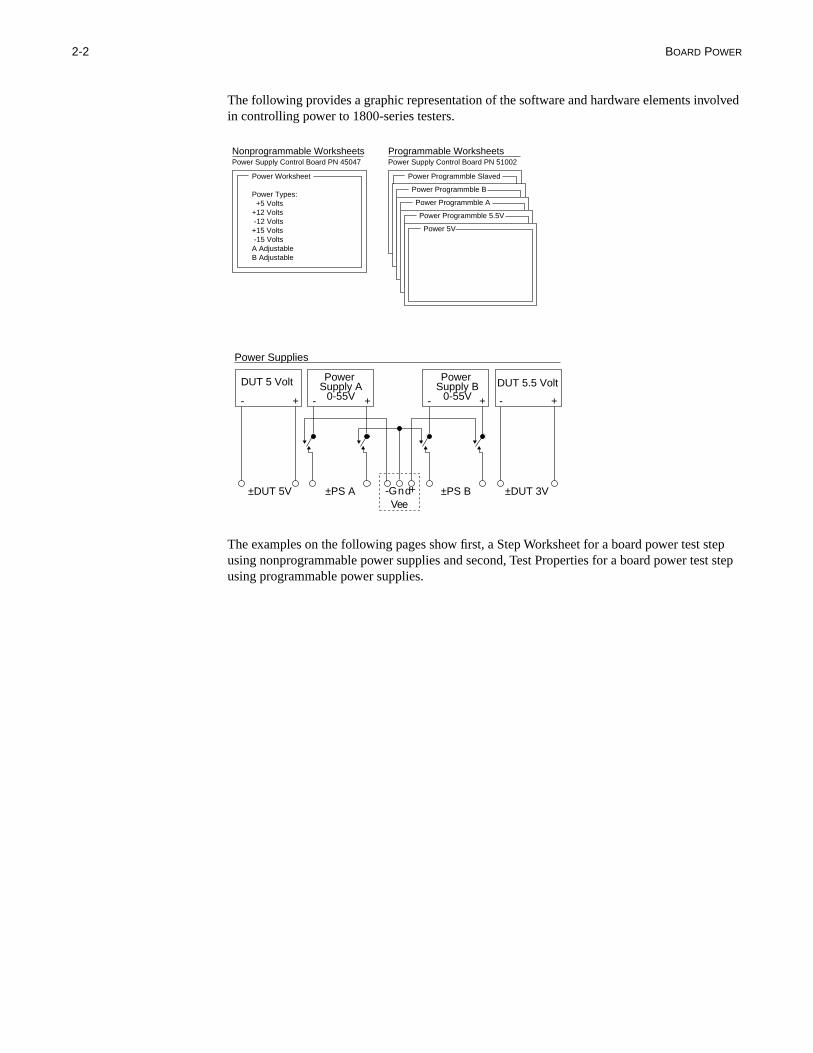
The following provides a graphic representation of the software and hardware elements invin controlling power to 1800-series testers.
The examples on the following pages show first, a Step Worksheet for a board power test susing nonprogrammable power supplies and second, Test Properties for a board power teusing programmable power supplies.
Nonprogrammable WorksheetsPower Supply Control Board PN 45047
Power Worksheet
Power Types: +5 Volts+12 Volts -12 Volts+15 Volts -15 VoltsA AdjustableB Adjustable
Programmable WorksheetsPower Supply Control Board PN 51002
Power Programmble Slaved
Power Programmble B
Power Programmble A
Power Programmble 5.5V
Power 5V
DUT 5 Volt
Power Supplies
DUT 5.5 VoltPower Supply A
0-55V
Power Supply B
0-55V- + - +
- +
- + - +
VeeGnd±DUT 5V ±PS A ±PS B ±DUT 3V

2-3
Below is an example of a nonprogrammable power supply Step Worksheet.
18xx Windows mode-init_com
Page 1 of 1
Test DataMeasureReferenceWait (ms)
:::
Pin 1 (21)
Edit Options Tools Revert Validate QuitSave
Component Properties
Test Properties Options Indicators
Pre Post CntrlCurrent Page
START CANCEL SOF HLD RPT CRT
Adjustable PS AAdjustable PS BAnalog TemplateDigFuncProcFixed/Slaved PS AFixed/Slaved PS BPBPower 5.5VPower 5VPower Bus
ScaleHighLow
V5.54.5
Power Type: +5 Volts MeasureReferenceWait (ms)
:::
:::
Pin 1 (21)
Test Type: Power
+ 5 Volts+12 Volts–12 Volts+15 Volts–15 VoltsA AdjustableB AdjustableMeas Only
+ID: Name: Desc:
Device Type:Number of Pins:
5 Volt 5 volt Vcc supply Vcc supply for logic test
Power 5V1
uvmvV
DigFuncProcExternal ProgramIEEENo TestPowerPower 5V
Power Prog 5.5VPower Prog APower Prog BPower Prog SlavedTest V
C:\TPD\DEMO-ICT
Default6 decimal
Z1800-Series Component Test Reference

2-4 BOARD POWER
st step.
Below is an example of a programmable power supply Test Properties. The Component Properties portion of the Step Worksheet is the same as for the adjustable power supply te18xx Windows mode-init_com
Page 1 of 2
Test Data
Controls
Edit Options Tools Revert Validate QuitSave
Component Properties
Test Properties Options Indicators
Pre Post CntrlCurrent Page
START CANCEL SOF HLD RPT CRT
OnOff
Test Type: Prog 5V
HighLow
Mode
Wait (ms)
5.254.75
:::
OnOn
C:\TPD\DEMO-ICT

2-5
s the nique to
Editing Test Properties The Test Properties portion of the Step Worksheet for both types of power supplies containparameters to execute the test step. The table below describes the Test Properties’ fields uBoard power.
Upper Test Properties Area
Field Description
Test Type Test configuration for the current Test Properties page. For board power:
No Test No Test executed. Wait state possible, however.
Power Shorthand power test step. Not programmable.
Power 5V Test for DUT 5V power supply. Not programmable.
Power Prog 5.5V Test for use with 3 V optional power supply. Programmable range 0–5.5 volts.
Power Prog A Test for power supply A. Programmable range: 0-55 volts.
Power Prog B Test for power supply B. Programmable range: 0–55 volts.
Power Prog Slaved Test for slaved A and B power supplies. Programmable range: 0–55 volts.
Test V Longhand voltage test. Also test type for second and third pages of programmable test types to measure voltage at DUT.
Test Data/ Middle Test Properties Area
Power Test Type: For use with Power Supply Controller PN 45047
Scale Power unit modifier—uv, mv, V.
High Upper limit of a passing measurement.
Low Lower limit of a passing measurement.
Power Type Specifies power supply. Choices are:+5 Volts, +12 Volts, -12 Volts, +15 Volts, -15 Volts, A Adjustable, B Adjustable.
Measure Pin/node number(s) at which measurement is taken. 5 nodes max.
Reference Pin/node number(s) of ground reference point(s). 10 nodes max. If no measurement given, measurement is referenced to system ground
Wait (ms) 0 to 32000 ms. Added to default wait of 3 ms typical.
Power 5 Test Type For use with PS controller PN 51002. Same fields as Power Prog test types, but without the Value field. Functions like Power Type +5 Volts.
Power Prog Test Types
For use with PS controller PN 51002. Power Prog A, Power Prog B, and Power Prog Slaved
Value (V) Enter desired value, 0–55 volts for Power Prog A, Power Prog B, and Power Prog Slaved; 0–5.5 volts for 3 volt option.
High Upper limit of a passing measurement. Always stated in actual value, not percent
Low Lower limit of a passing measurement. Always stated in actual value, not percent.
Mode Enables selection of connection of power supply to output pins (On/Off); disables or reenables power supply (Disable/Enable); changes voltage for programmable power supplies without changing state of connection (Reprogram).
Wait (ms) Same as adjustable Power test type.
Test V Test Type Contains all Power fields except Power Type.
Z1800-Series Component Test Reference
2-6 BOARD POWER
tem ower
out eld in
in the
rnal) to
A refer
with ttings.
PSB
m a V the a.
Refer to the Z1800-Series Programmer’s Guidebook , Chapter 3, for further details about StepWorksheet fields not discussed here.
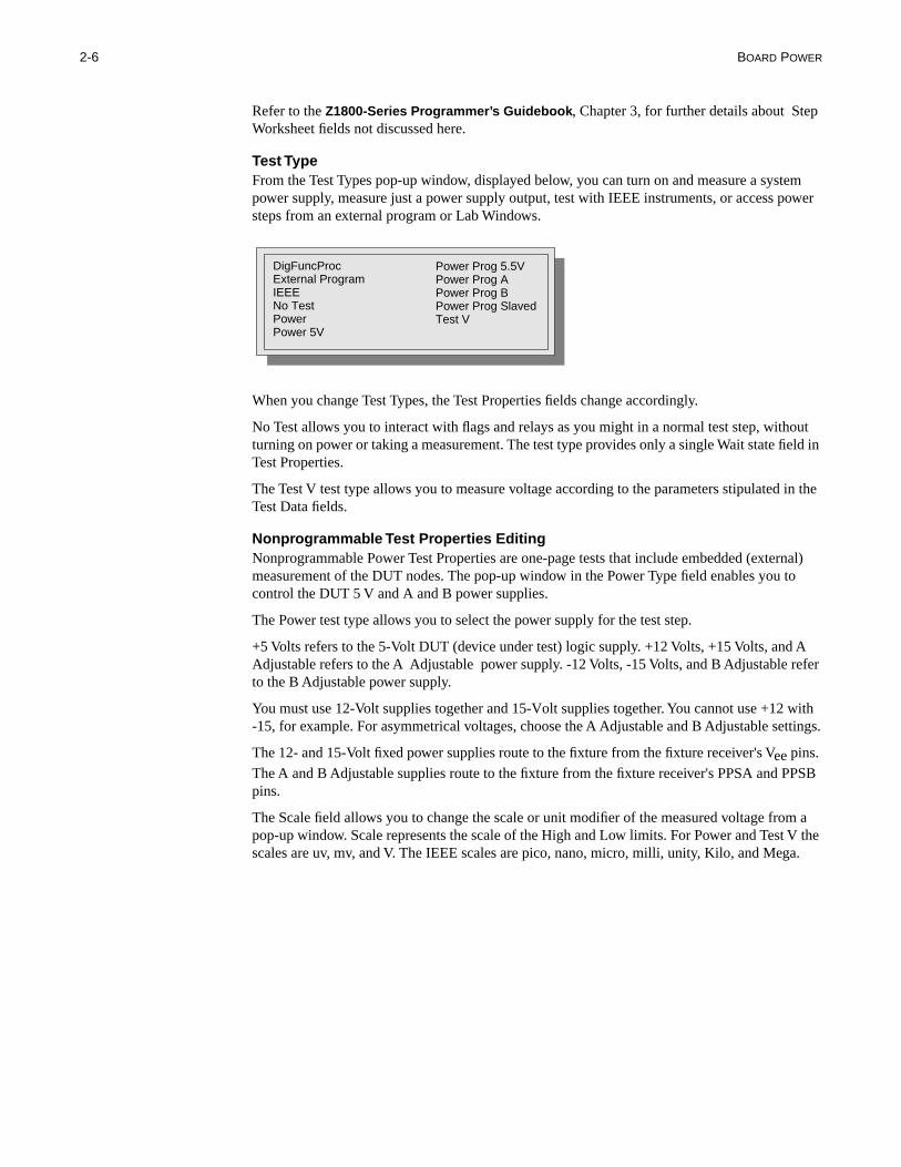
Test TypeFrom the Test Types pop-up window, displayed below, you can turn on and measure a syspower supply, measure just a power supply output, test with IEEE instruments, or access psteps from an external program or Lab Windows.
When you change Test Types, the Test Properties fields change accordingly.
No Test allows you to interact with flags and relays as you might in a normal test step, withturning on power or taking a measurement. The test type provides only a single Wait state fiTest Properties.
The Test V test type allows you to measure voltage according to the parameters stipulatedTest Data fields.
Nonprogrammable Test Properties EditingNonprogrammable Power Test Properties are one-page tests that include embedded (extemeasurement of the DUT nodes. The pop-up window in the Power Type field enables you control the DUT 5 V and A and B power supplies.
The Power test type allows you to select the power supply for the test step.
+5 Volts refers to the 5-Volt DUT (device under test) logic supply. +12 Volts, +15 Volts, and Adjustable refers to the A Adjustable power supply. -12 Volts, -15 Volts, and B Adjustable to the B Adjustable power supply.
You must use 12-Volt supplies together and 15-Volt supplies together. You cannot use +12-15, for example. For asymmetrical voltages, choose the A Adjustable and B Adjustable se
The 12- and 15-Volt fixed power supplies route to the fixture from the fixture receiver's Vee pins.
The A and B Adjustable supplies route to the fixture from the fixture receiver's PPSA and Ppins.
The Scale field allows you to change the scale or unit modifier of the measured voltage fropop-up window. Scale represents the scale of the High and Low limits. For Power and Testscales are uv, mv, and V. The IEEE scales are pico, nano, micro, milli, unity, Kilo, and Meg
DigFuncProcExternal ProgramIEEENo TestPowerPower 5V
Power Prog 5.5VPower Prog APower Prog BPower Prog SlavedTest V
2-7
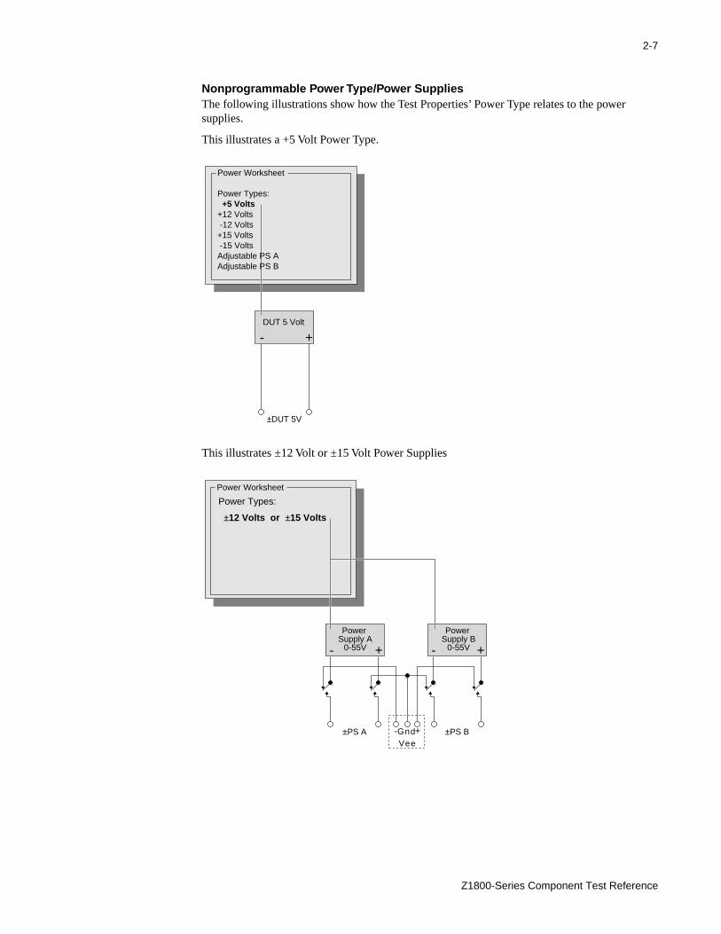
Nonprogrammable Power Type/Power SuppliesThe following illustrations show how the Test Properties’ Power Type relates to the power supplies.
This illustrates a +5 Volt Power Type.
This illustrates ±12 Volt or ±15 Volt Power Supplies
- +
±DUT 5V
Power Worksheet
Power Types: +5 Volts+12 Volts -12 Volts+15 Volts -15 VoltsAdjustable PS AAdjustable PS B
DUT 5 Volt
- +
- +
- +
VeeGnd±PS A ±PS B
Power Worksheet
Power Types:
±12 Volts or ±15 Volts
Power Supply A
0-55V
Power Supply B
0-55V
Z1800-Series Component Test Reference

2-8 BOARD POWER
r e-page er
elds l s
er is
tly er
tage ower the sure to the
This illustrates A Adjustable and B Adjustable Power Types.
Programmable Power Supplies—Test Properties EditingControl of the programmable power supplies is exercised through the programmable powesupply Test Properties. These two-page (Power Prog 5.5 and Power Prog A and B) or thre(Power Prog Slaved) tests make an internal measurement of the DUT directly from the powsupply in addition to controlling the application of power.
All Test Properties that control the Power Supply Controller PN 51002 have high and low fithat are used as thresholds for the internal voltage measurement. They also have a controselection with the minimum choices of On or Off (Power 5V); programmable power suppliehave Enable, Disable, and Reprogram functions. In addition a Wait time is available.
Internal Measurements—Low/High Thresholds . All power supply Test Properties that controlPower Supply Controller Board PN 51002 conduct an internal measurement whenever powturned on, enabled, or reprogrammed. The measurement path for this voltage comes direcfrom the power supply controller and measures the voltage directly at the output of the powsupply. Depending on the placement of the sense lines and the amount of current, this volwill vary from the voltage on the DUT. This measurement should be used to verify that the psupply is working. For all internal measurements, the low/high thresholds are derived fromrequested tolerance plus 15% for an internal measurement of the supply. To precisely meathe voltage on the DUT, the Test V measurement on a subsequent page (or pages) is doneuser-specified tolerance(s).
Wait Time . The Wait time (0–32,000 ms) applies after a power supply has been turned on, enabled, or reprogrammed and before the internal measurement takes place.
- +
- +
- +
VeeGnd±PS A ±PS B
Power Worksheet
Power Types:
A Adjustable
B Adjustable
Power Supply A
0-55V
Power Supply B
0-55V
2-9
efore a
the
ing
.5 V ge 2
.
.5
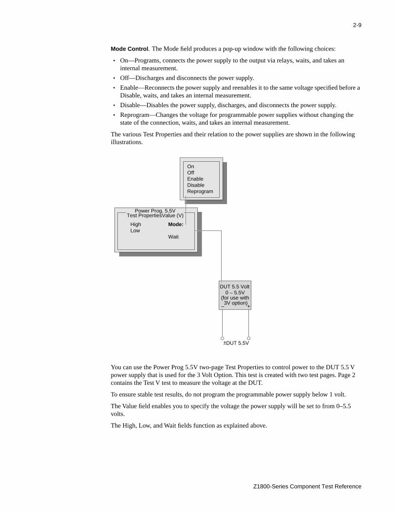
Mode Control . The Mode field produces a pop-up window with the following choices:
• On—Programs, connects the power supply to the output via relays, waits, and takes aninternal measurement.
• Off—Discharges and disconnects the power supply.
• Enable—Reconnects the power supply and reenables it to the same voltage specified bDisable, waits, and takes an internal measurement.
• Disable—Disables the power supply, discharges, and disconnects the power supply.
• Reprogram—Changes the voltage for programmable power supplies without changing state of the connection, waits, and takes an internal measurement.
The various Test Properties and their relation to the power supplies are shown in the followillustrations.
You can use the Power Prog 5.5V two-page Test Properties to control power to the DUT 5power supply that is used for the 3 Volt Option. This test is created with two test pages. Pacontains the Test V test to measure the voltage at the DUT.
To ensure stable test results, do not program the programmable power supply below 1 volt
The Value field enables you to specify the voltage the power supply will be set to from 0–5volts.
The High, Low, and Wait fields function as explained above.
OnOffEnableDisableReprogram
– +
±DUT 5.5V
Power Prog. 5.5VTest PropertiesValue (V)
Mode:
Wait
HighLow
DUT 5.5 Volt0 – 5.5V
(for use with 3V option)
Z1800-Series Component Test Reference
2-10 BOARD POWER
tively. relays.
est
st
have the e, use
est
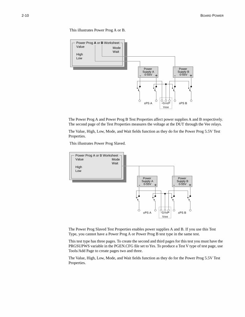
This illustrates Power Prog A or B.
The Power Prog A and Power Prog B Test Properties affect power supplies A and B respecThe second page of the Test Properties measures the voltage at the DUT through the Vee
The Value, High, Low, Mode, and Wait fields function as they do for the Power Prog 5.5V TProperties.
This illustrates Power Prog Slaved.
The Power Prog Slaved Test Properties enables power supplies A and B. If you use this TeType, you cannot have a Power Prog A or Power Prog B test type in the same test.
This test type has three pages. To create the second and third pages for this test you must PRGSUPWS variable in the PGEN.CFG file set to Yes. To produce a Test V type of test pagTools/Add Page to create pages two and three.
The Value, High, Low, Mode, and Wait fields function as they do for the Power Prog 5.5V TProperties.
- +
- +
- +
VeeGnd±PS A ±PS B
Power Supply A
0-55V
Power Supply B
0-55V
Power Prog A or B WorksheetValue
HighLow
ModeWait
- +
- +
- +
VeeGnd±PS A ±PS B
Power Supply A
0-55V
Power Supply B
0-55V
Power Prog A or B WorksheetValue
HighLow
ModeWait

2-11
the in
e
e
This illustrates Power 5V.
The Power 5 Test Properties turns power on and off to the DUT 5 volt power supply using programmable power supply controller PN 51002. It functions like the Power Type +5 Voltsthe Power Test Properties.
The High and Low fields function as they do for Power Prog 5.5V.
Use the Power 5 Mode field pop-up window to select On or Off to connect or disconnect thpower supply to the output pins via relays.
The Wait field allows you to specify a wait state from 0 to 32,000 ms. Wait happens after thpower is turned on and before the internal measurement is concluded.
OnOff
– +
±DUT 5.5V
Power 5V Worksheet
Mode:Wait
HighLow
DUT 5 Volt
Z1800-Series Component Test Reference

The ce the ut the
in Test field in n test.
e ing
and
3 CAPACITORS
Capacitor tests can be divided into two basic modes of testing—shorthand and longhand. shorthand modes are component-type specific and offer the best possible performance sinoperating system can make certain assumptions about the component under test and aboway the test system is applied to test it.
You can use the following shorthand test modes for capacitor tests:
• Capacitor
• Extended
• Cap Phase
You can access the Capacitor and Cap Phase modes through their respective Test Types Properties. To enable Extended mode, select Extended/Yes in to the right of the Test Type Test Properties. Each of these modes has an option for resistor/capacitor (RC) combinatio
Longhand tests, while available for capacitor testing, have certain disadvantages in that thlonghand test types do not have built-in programming to automatically compensate for varyeffects of board and system capacitance on the device under test.
Test Type: Capacitor Functionality
• Basic test type for capacitors from 10 pF to (end of range)
• Two modes of operation—AC or DC change up
• Fastest test type (Fast Mode On increases execution speed)
• Basic RC test capability
• Auto-ranging with Extended On
• Specifiable V_dut Pk–Pk with Extended On
Test Type: Cap Phase Functionality
• Improved low end, single digit pF to 99.9 nF
• Improved test for RC combinations
• Improved precision and stability (speed is not as great as with the Capacitor test type)
• Test Properties Offset Cap compensates for capacitance in the fixture
The PRISM-Z (PRecision Integrated Signal Measurement) module is available as an optioncan be used for Capacitor tests. Refer to the Z1800-Series PRISM-Z User’s Guide for a complete discussion about the PRISM-Z test types available for Capacitor tests.
3-2 CAPACITORS
. The
r's low wever, sidual nt. This igher,
ement. us See
e ulting
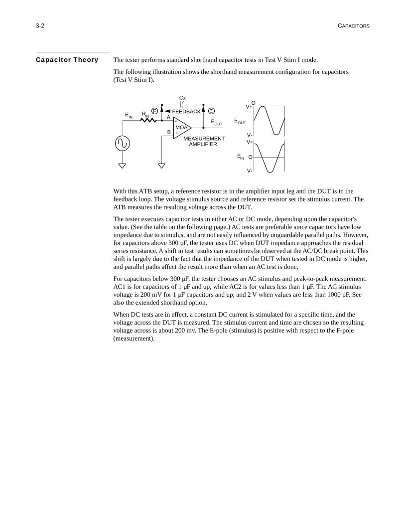
Capacitor Theory The tester performs standard shorthand capacitor tests in Test V Stim I mode.
The following illustration shows the shorthand measurement configuration for capacitors (Test V Stim I).
With this ATB setup, a reference resistor is in the amplifier input leg and the DUT is in the feedback loop. The voltage stimulus source and reference resistor set the stimulus currentATB measures the resulting voltage across the DUT.
The tester executes capacitor tests in either AC or DC mode, depending upon the capacitovalue. (See the table on the following page.) AC tests are preferable since capacitors haveimpedance due to stimulus, and are not easily influenced by unguardable parallel paths. Hofor capacitors above 300 µF, the tester uses DC when DUT impedance approaches the reseries resistance. A shift in test results can sometimes be observed at the AC/DC break poishift is largely due to the fact that the impedance of the DUT when tested in DC mode is hand parallel paths affect the result more than when an AC test is done.
For capacitors below 300 µF, the tester chooses an AC stimulus and peak-to-peak measurAC1 is for capacitors of 1 µF and up, while AC2 is for values less than 1 µF. The AC stimulvoltage is 200 mV for 1 µF capacitors and up, and 2 V when values are less than 1000 pF.also the extended shorthand option.
When DC tests are in effect, a constant DC current is stimulated for a specific time, and thvoltage across the DUT is measured. The stimulus current and time are chosen so the resvoltage across is about 200 mv. The E-pole (stimulus) is positive with respect to the F-pole(measurement).
+
-MOA
A
B
FEEDBACK
MEASUREMENTAMPLIFIER
EOUT
EIN
RIN
F E
Cx
V-
V+
V-
O
O
V+
OUTE
EIN
3-3
hnique within
est. To p
e a
50 µF
. The isplays
ered in ade.
ces in ap
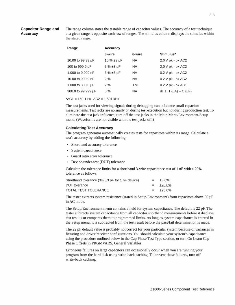
Capacitor Range and Accuracy
The range column states the testable range of capacitor values. The accuracy of a test tecat a given range is opposite each row of ranges. The stimulus column displays the stimulusthe stated range.
*AC1 = 159.1 Hz; AC2 = 1.591 kHz
The test jacks used for viewing signals during debugging can influence small capacitor measurements. Test jacks are normally on during test execution but not during production teliminate the test jack influence, turn off the test jacks in the Main Menu/Environment/Setumenu. (Waveforms are not visible with the test jacks off.)
Calculating Test AccuracyThe program generator automatically creates tests for capacitors within its range. Calculattest's accuracy by adding the following:
• Shorthand accuracy tolerance
• System capacitance
• Guard ratio error tolerance
• Device-under-test (DUT) tolerance
Calculate the tolerance limits for a shorthand 3-wire capacitance test of 1 nF with a 20% tolerance as follows:
Shorthand tolerance (3% ±3 pF for 1 nF device) = ±3.0%DUT tolerance = ±20.0%TOTAL TEST TOLERANCE = ±23.0%
The tester extracts system resistance (stated in Setup/Environment) from capacitors abovein AC mode.
The Setup/Environment menu contains a field for system capacitance. The default is 22 pFtester subtracts system capacitance from all capacitor shorthand measurements before it dtest results or compares them to programmed limits. As long as system capacitance is entthe Setup menu, it is subtracted from the test result before the pass/fail determination is m
The 22 pF default value is probably not correct for your particular system because of varianfixturing and driver/receiver configurations. You should calculate your system’s capacitanceusing the procedure outlined below in the Cap Phase Test Type section, or turn On Learn CPhase Offsets in PRGMVARS, General Variables.
Erroneous failures on large capacitors can occasionally occur when you are running your program from the hard disk using write-back caching. To prevent these failures, turn off write-back caching.
Range Accuracy
3-wire 6-wire Stimulus*
10.00 to 99.99 pF 10 % ±3 pF NA 2.0 V pk - pk AC2
100 to 999.9 pF 5 % ±3 pF NA 2.0 V pk - pk AC2
1.000 to 9.999 nF 3 % ±3 pF NA 0.2 V pk - pk AC2
10.00 to 999.9 nF 2 % NA 0.2 V pk - pk AC2
1.000 to 300.0 µF 2 % 1 % 0.2 V pk - pk AC1
300.0 to 99,999 µF 5 % NA dc 1, 1 (µA) = C (µF)
Z1800-Series Component Test Reference
3-4 CAPACITORS
egory. est type
Step Worksheet Editing
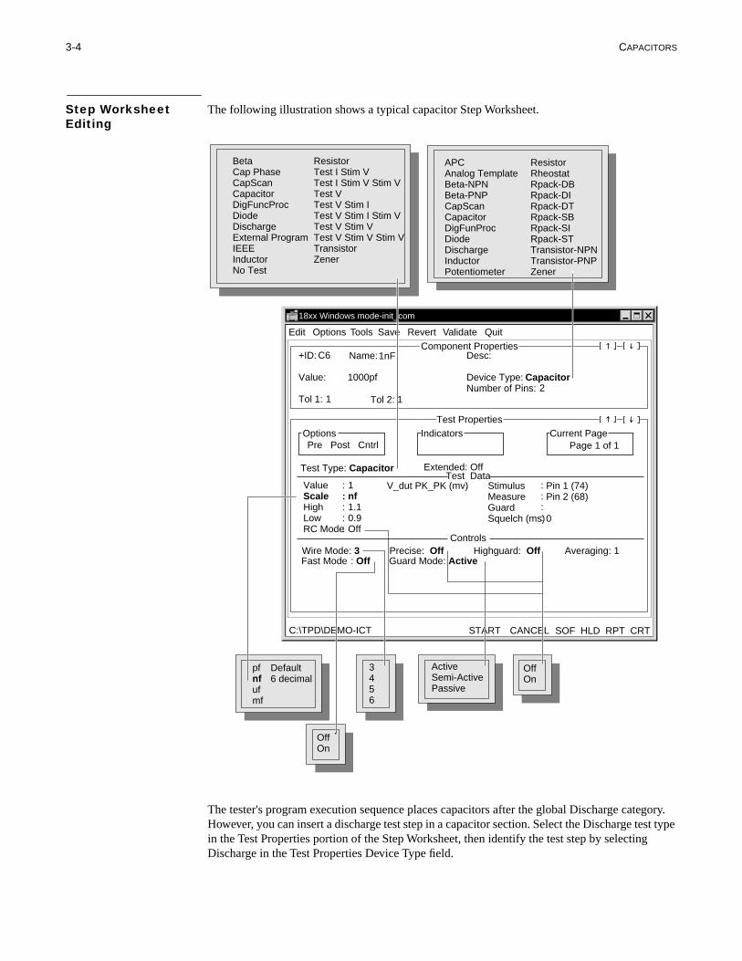
The following illustration shows a typical capacitor Step Worksheet.
The tester's program execution sequence places capacitors after the global Discharge catHowever, you can insert a discharge test step in a capacitor section. Select the Discharge tin the Test Properties portion of the Step Worksheet, then identify the test step by selectingDischarge in the Test Properties Device Type field.
18xx Windows mode-init_com
Page 1 of 1
Test Data
Controls
Edit Options Tools Revert Validate QuitSave
Component Properties
Test Properties Options Indicators
Pre Post CntrlCurrent Page
START CANCEL SOF HLD RPT CRT
Test Type: Capacitor
C:\TPD\DEMO-ICT
+ID:
Value:
Tol 1:
Name: Desc:
Device Type:Number of Pins:
C6 1nF
1000pf Capacitor2
Tol 2:1 1
APCAnalog TemplateBeta-NPNBeta-PNPCapScanCapacitorDigFunProcDiodeDischargeInductorPotentiometer
ResistorRheostatRpack-DBRpack-DIRpack-DTRpack-SBRpack-SIRpack-STTransistor-NPNTransistor-PNPZener
BetaCap PhaseCapScanCapacitorDigFuncProcDiodeDischargeExternal ProgramIEEEInductorNo Test
ResistorTest I Stim VTest I Stim V Stim VTest VTest V Stim ITest V Stim I Stim VTest V Stim VTest V Stim V Stim VTransistorZener
Extended: Off
ValueScaleHighLowRC Mode
1nf1.10.9Off
StimulusMeasureGuardSquelch (ms)
:::::
::::
Pin 1 (74)Pin 2 (68)
0
V_dut PK_PK (mv):
pfnfufmf
Wire Mode: 3 Precise: Off Highguard: Off Averaging: 1Fast Mode : Off Guard Mode: Active
3456
ActiveSemi-ActivePassive
OffOn
OffOn
Default6 decimal

3-5
l.
rance 1
he
Component Properties The Component Properties for capacitor test operates as it does for analog tests in genera
Refer to the Z1800-Series Programmer’s Guidebook , Chapter 3, for specific details about editing Component Properties for analog tests.
Because capacitors often have asymmetric tolerances, there are two tolerance fields. Tole(Tol 1) is the plus or high tolerance; Tolerance 2 (Tol 2) is the minus or low tolerance.
The Tol 1 and Tol 2 fields are entry fields. Highlight the fields with the cursor, and enter theappropriate one- or two-digit numbers for the respective plus and minus percent tolerance.
Test Properties Test Properties for capacitor test operates as it does for analog tests in general except in tinstances listed below in the table, Capacitor Test Properties fields.
Refer to the Z1800-Series Programmer’s Guidebook , Chapter 3, for details about analog TestProperties fields.
Field Type Description Data Source*
+/• Enable/Disable Test Step
+ Step is enabled for testing• Step is disabled for testing
Click to select.
ID: Text. Max=8 Capacitor test step identification.
Input list ID field
Name: Text. Max=20 Capacitor test step name Input list CN field
Desc: Text. Max=64 String for commenting Input list quoted string
Value: Text. Max=6. Pop-up
Capacitor valuepf, nf, uf, mfDefault, 6 decimal
Input list VAL1
Tol 1: & Tol 2: Text Capacitor tolerance TOL1 and TOL2 fields
Device Type: Pop-up** Type of device test C field (capacitor)
Number of Pins: Text**. Max=128† Number of device pins NODES field
Upper Test Properties Area
Field Description
Test Type: Type of test configuration used on current Test Properties page. Recommended for capacitors:
Capacitor For shorthand capacitor test.
Cap Phase For testing small value capacitors and RC combinations.
Extended Enables extended shorthand test. Default is Off.
Shorthand and Extended Shorthand Test DataMiddle Test Properties Area
Value A numeric field specifying the nominal expected value of Scale. Range = 0 – 999.
Scale Value field’s unit modifier based on Capacitor Test Type: pf, nf, uf, mf
RC Mode ON or OFF. When ON, activates parallel resistor/capacitor test.
V_dut Pk–Pk (mv) A numeric field to specify voltage across the capacitor. Range = 40–800 mV. Default = 200 mV. (For extended shorthand test)
Controls/Lower Test Properties Area
Fast Mode ON or OFF. Default is OFF. When ON, test runs without built-in Wait and Squelch times.
Z1800-Series Component Test Reference

3-6 CAPACITORS
res ment onent
ase uses s better rallel
pe
k–peak
de only e 1 and
t nt
in um
the
itor is pplied en and
at the ld in
the
ding
Upper Test Properties AreaTest Type Field . The Capacitor Test Type is a shorthand test type that automatically configuthe ATB to the Test V Stim I test mode. The appropriate stimulus frequency, limits, measurevoltage, measurement scale, and computing resistor are also selected, based on the compvalue and the tolerances.
The Cap Phase Test Type is a special version of the shorthand capacitor test type. Cap Pha phase angle measurement to determine the capacitor value. In general Cap Phase workthan the standard capacitor measurement type for small, difficult-to-read capacitors with paresistance. For more information about Cap Phase testing, refer to the Cap Phase Test Tysection on page 13.
Extended Field . The Extended field enables you to enable or disable extended shorthand capacitor test. This is an On/Off field with the default state being Off.
In the On state, another field is turned on in the Test Data area where you can enter the peameasurement voltage in millivolts.
Test Data AreaThe RC Mode field allows you to select parallel resistor/capacitor mode. Select the RC Mofield and select either On or Off. RC mode is off by default. The RC Mode field is available in shorthand capacitor test type. It requires a shorthand resistor test on Test Properties paga shorthand capacitor test on Test Properties page 2 of the Step Worksheet.
SquelchRefer to the Z1800-Series Programmer’s Guidebook , Chapter 5, for detailed information abouthe effects of Squelch on Capacitor tests see the discussion of general analog measuremeconcepts.
Controls AreaThe Fast Mode field, when set to On, suppresses built-in Wait and Squelch times resultingfaster test execution. Depending on the value of the component to be measured, the minimWait times that are built into to the system software vary from 1 to 200 milliseconds. WhenFast Mode field is set to the default Off, the test executes with the built-in Wait and Squelchtimes.
Extended Shorthand Test Mode
For capacitors smaller than 1000 pF, the stimulus voltage is approximately 2 V. The higherstimulus voltage prevents the use of an internal limiter circuit. If a less-than-1000 pF capacmissing from the board (due to a broken lead, for example), high stimulus voltage may be ato the surrounding circuitry. In addition, the high stimulus voltage (2 V) poses a problem whtesting these small capacitors in the vicinity of semiconductors that start to conduct at 0.7 Vcause a guarding problem.
To overcome both of these problems, the capacitor test has an Extended option. When theExtended option in Test Properties is On, the stimulus current is autoranged to the point thvoltage across the device under test matches the voltage requested in the V_dut Pk–Pk fieTest Properties. Then a regular capacitor measurement is performed. During autoranging,internal limiter circuit is in effect to limit the voltage on the DUT to less than 2 V Pk–Pk. Theallowable V_dut is between 40 mV and 800 mV to prevent conflict with semiconductor guarpaths.

3-7
meters. ly
tim I e of
F, the rove e pacitor
V he es act option
rent in
test.
as
erance
g
Test Parameters To see the actual test parameters used for a particular capacitor test, select Tools/Test ParaA window displays the voltages, currents, and frequency involved in the test for the currentdisplayed Test Properties page.
As mentioned in the foregoing discussion of capacitor testing, the ATB is set up in Test V Smode for stability reasons. The stimulus (current and frequency) is chosen to yield a voltagapproximately 200 mv Pk–Pk across the DUT. However, for capacitor values below 1000pstimulus is chosen in order to yield approximately 2 V Pk-Pk. A higher voltage is used to impthe signal-to-noise ratio for small capacitors. The voltage is said to be approximate since thprecise value depends on the value of the capacitor under test; a smaller than expected cavalue will result in a higher than expected voltage. This moving voltage and the fact that 2 Pk-Pk is used for small capacitors create a guarding problem when the DUT is located in tvicinity of semiconductors such as diodes, transistors, and integrated circuits. These devicas parallel unguardable paths as soon as the voltage reaches about 500 mv. The extendedon the Capacitor Test Properties page solves this problem by autoranging the stimulus curorder to yield the voltage across the DUT as specified in the V_dut field in Test Properties.
During the autoranging process, the maximum voltage across the DUT is limited to approximately 2 V Pk-Pk for protection of the surrounding components on the board underV_Dut should be programmed as high as possible but not high enough to turn on any semiconductor junctions. 300mV is a good starting value. When the autoranging process hended, a final measurement is taken without the limiter circuit.
The autoranging effect of extended mode provides an additional benefit because a wide tolcapacitor can be tested without losing precision at either end of the thresholds.
DrawbacksExtended mode test takes slightly longer than regular shorthand because of the autorangininvolved.
Extended mode is applicable only for capacitors measured with the AC technique used forcapacitors from 10pF to 300uF.
There is no extended option available for the Cap Phase test type.
Z1800-Series Component Test Reference
3-8 CAPACITORS
orthand
ou to
e he e
or
st type C
Worksheet Editing The extended shorthand mode uses all of the test page fields as described above in the shtest editing section plus two others: the Extended field and the V_dut Pk–PK field.
The Extended field in the upper area of Test Properties allows you to enable or disable theextended mode for capacitor test. It is an On/Off field, with the default state being Off.
In the On state, another field in the Test Data area of Test Properties is enabled allowing yspecify the measurement voltage, in millivolts.
The extended shorthand capacitor mode field V_dut Pk–Pk is enabled when the Extended modfield is turned on. It enables you to specify a measurement peak–peak voltage other than tdefault voltage (usually 200 mv Pk–Pk as the lower limit) used by the system software. Thsystem software still specifies the measurement (Pk–Pk) and stimulus types (AC), and thecomputing resistor.
Cap Phase Test Type
The Extended Analog Assembly (EAA) (formerly referred to as the Extended Analog Option—EAO) allows for greatly improved precision and stability in testing of small capacitand RC combinations. Enhancements include
• Measurement as low as 2pF
• Improved reading stability
• Measurement with a parallel resistor range extended approximately 100 times
Although the RC-Phase board (Extended Analog Assembly) by means of the Cap Phase teenables you to choose a more precise measurement technique for small capacitors and R
18xx Windows mode-init_com
Page 1 of 1
Test Data
Controls
Test Type: Capacitor
Edit Options Tools Revert Validate QuitSave
Component Properties
Test Properties Options Indicators
Pre Post CntrlCurrent Page
START CANCEL SOF HLD RPT CRTC:\TPD\DEMO-ICT
OffOn
Test Type: Capacitor Extended: On
ValueScale HighLow
::::
nf1.1000.900
V_dut Pk-Pk (mv) : 200 StimulusMeasureGuardSquelch (ms)
::::
Pin 2 (68)Pin1 (74)
0

3-9
itors is t a
can of
combinations, the increased accuracy does affect speed. The overall range for small capacsingle digit pF to 99.9 nF. On RC combinations, the range is specified in bulk impedance afrequency of AC3 (15.59 kHz); the range is from 333 kΩ to 21.5 Ω. The technique permits testing to tight tolerances of a few percent.
For following illustrates an ATB Cap Phase Mode Block Diagram.
EAA Specifications StimulusOpen circuit voltage Approx. 700mVNominal DUT voltage <215mVpFrequency 15.915 kHz (AC3)
GuardPoles 3-wire onlyReference GNDMax. guard current <30mAMin. guard impedance >20Ω at 15.915kHzMax. guard capacitance 5nF
Phase angle must be > 45 degrees at 1MHz
Error MessagesTests will not run if an error condition is detected. The DUT TC/Phase Angle too low error be overridden by adjusting the low test limits to a TC > 100ns. However, there is a danger failing good components.
DUT TC Phase Angle Too Low (<100ns)DUT C Plus Csys Too Low (<33pF)DUT Z Too Low (<90Ω)DUT Z Too High (>300kΩ)
ATB
RefData DAC
ProgramResistor1K – 1M Compliance
Limit Freq.Comp.
Ref AmpX 10X 4.644X 2.155
+
– X 30.1
Y
X
MultiplierXY10
ADC Data
X1
PhaseChange
Resistors
Extended Analog Option ATB
GD FD EDDUT
100 – 215 mV pK
90 PhaseShift
+
–
+
– ProgramResistorPhase
Correction
Filter
Z1800-Series Component Test Reference

3-10 CAPACITORS
and the
and the
CapacitorTolerance is for the total measured capacitance that includes both the system capacitanceDUT capacitance.
Range 7pF to 99.9nF
(System capacitance and DUT capacitance combined must be >33pF.)
Accuracy18XX 5% ±2pF1884 or 18XX with 7% ±3pF
DR1 or DR2PStability 0.5% ±0.1pFSystem capacitance Approx. 40pF subtracted
Resistor/Capacitor
Tolerance is for the total measured capacitance that includes both the system capacitanceDUT capacitance.
RangeCapacitance 7pF to 99.9nF
(System capacitance and DUT capacitance combined must be > 33pF.)
Impedance 90Ω to 300kΩResistance ≥100Ω
Capacitance Accuracy
Phase = arc tan (Rdut/Xc)Where: Xc = 1/100,000 CdutClow = lowest capacitance that can be measured in the range combined with SysCap.TC = (Csys + Clowtol) * RdutWhere: Csys = Measured System capacitance
Clowtol = Lower limit of capacitor measure toleranceRdut = Measured DUT resistance
Stability 0.5% ±0.1pFSystem Capacitance Approx. 40pF subtractedResistor Accuracy Standard ATB accuracy
Phase Clow TC Accuracy
18XX 1884 or 18XX withDR1 or DR2P
>45° >7pF >10µs 6% ±3pF 7% ±3pF
>5.71° >10pF >1.0µs 8% ±5pF No Change
>2.86° >15pF >500ns 12% ±7pF No Change
>1.15° >25pF >200ns 18% ±10pF No Change
>0.573° >35pF >100ns 25% ±12pF No Change

3-11
ance
Resistor/Capacitor Tolerance Calculation
1 Calculate the Time Constant (TC).
TC = Rdut value* Cdut value
2 Determine the appropriate range.
Example: If TC ≥ 200ns, use range >200ns.
3 Determine the typical Csys.
Csys will typically be in the range of 33pF to 55pF. You can measure system capacitby doing a Learn Cap or by measuring typical system capacitance.
4 Calculate the low tolerance of capacitor test.
Example: If TC ≥ 200ns
Clowtol = Cdut – ((Cdut*Ctol) – ((Cdut + Csys)* 18%)) –10pF
where Ctol is the tolerance of Cdut
5 Calculate the TC for Clowtol.
TClow = (Csys + Clowtol)*Rdut
6 If TClow is > 100ns, proceed; otherwise the test may not be possible.
7 Calculate the high tolerance of capacitor test.
Example: If TC ≥ 200ns
Chightol = Cdut + ((Cdut*Ctol) + ((Cdut + Csys)*18%)) +10pF
Typical Measurement AccuracyAssumes: Csys = 40pF, No Cdut tolerance included
DUT R/C Phase TC Capacitor Tolerance
10pF NA NA 5.5–14.5pF
1.0M/10pF >45° >10µs 4.0–16pF
100k/10pF >5.71° >1µs 1.0–19pF
50k/10pF >2.86° >500ns Clow = 15pF
20k/10pF >1.15° >200ns Clow = 25pF
10k/10pF >0.573° >100ns Clow = 35pF
100pF NA NA 91.0–109pF
100k/100pF >45° >10µs 88–111pF
10k/100pF >5.71° >1µs 83–116pF
5k/100pF >2.86° >500ns 76–124pF
2k/100pF >1.15° >200ns 65–135pF
1.1k/100pF >0.573° >100nµs 53–147pF
1nF NA NA 0.946–1.054nF
10k/1nF >45° >10µs 0.935–1.065nF
1k/1nF >5.71° >0µs 0.912–1.088nF
500/1nF >2.86° >500ns 0.868–1.132nF
200/1nF >1.15° >200ns 0.803–1.197nF
140/1nF >0.573° >100nµs 0.728–1.272nF
Z1800-Series Component Test Reference

3-12 CAPACITORS
The ng the
tor is
he
ation
rds the
extent test.
t an
Mode
that is, large. s a
and ith
allel RC he
ee
ees e gain s, then ing
the ide of
100 the
RC (Resistor/Capacitor) TestingCapacitors connected in parallel with resistors frequently appear on printed circuit boards.tester provides a method of testing these resistor/capacitor (RC) networks in two parts usishorthand Capacitor Worksheet as the basis for the test.
During autogeneration of an entire test program, Pgen looks for RC combinations. If a resisfound in parallel to a capacitor, the following automatically happens:
• The capacitor test is moved to a second page.
• The resistor test is copied from the resistor section into the vacated page number 1 in tcapacitor section.
• The original resistor test is disabled in the resistor section but is left there for documentpurposes.
The first page of an RC test measures the resistive component of the combination and recoresult internally. When debugging RC test combinations, you must measure the resistive component as precisely as possible by using wait times, averaging, and guarding to the fullsince the result of the measurement directly affects the precision of the following capacitor
There is an impedance ratio beyond which the resistor is ignored, and only a capacitor, noRC, test is generated.
The second page contains a capacitor test (Capacitor or Cap Phase test type) with the RCset to On. When this test is run, the result is mathematically modified with the previously measured resistive component to extract the capacitive component.
The extraction is most successful when the bulk impedance is dominated by the capacitor, when the phase angle between the current going through the resistor and the capacitor is The extraction becomes increasingly difficult as the phase angle decreases. Phase angle ifunction of the component values involved and the stimulus frequencies.
Capacitor measurements made using the Capacitor test type are generally done with AC1AC2. Capacitor measurements made using the Cap Phase test type are exclusively done wAC3, which improves RC test capability
Theory The EAA uses a phase measurement technique to extend the range of capacitors and parcombinations beyond what ATB can provide with its impedance measurement approach. TEAA operates at 15.915 kHz exclusively.
When phase detection is used, the ATB stimulus DAC is programmed to provide one of thrvoltages: 1.0 V, 2.155 V, or 4.644 V. The stimulus follows two paths through the circuit: the reference path and the measurement path. See Figure 7.14.
The reference path provides a 10 Vp signal to the Y input of the multiplier, which is 90 degrout of phase with the stimulus. The stimulus feeds an amplifier with three gain settings. Onsetting is selected to produce the 10 volt peak signal. This signal is phase-shifted 90 degreephase-compensated to ensure 90 degree phase shift with each of the four range programmresistors.
The measurement path connects the stimulus to the FD pole through one of the range programming resistors. The FD pole also connects to the DUT and to the summing junction of EAA measurement op amp. The EAA measurement op amp output connects to the other sthe DUT through the ED pole. The DUT is placed in the amplifier feedback loop in the same fashion as the ATB's Test V Stim I configuration. The voltage across the DUT will vary frommVp to 215 mVp, depending on the nominal DUT value. A 0.7 Vp compliance limit protectsDUT and surrounding circuitry from either missing or wrong value components.

3-13
key ch AC
ith the portion
tor test d the Use xture. enu is . The xture
also r the
ts that e ents in
The wide bandwidth EAA measurement op amp introduces negligible phase error, and is aelement in allowing effective phase measurement. Its output drives an X30.1 amplifier, whiconnects to the X input of the multiplier. The output of the multiplier is filtered to remove anycomponents. The resulting DC voltage is proportional to the current flowing through the capacitor being measured. The ATB measures this DC voltage.
Cap Phase for Capacitor and RC Tests
Testing a component using Cap Phase is similar to testing using the Capacitor test type wexception that you can specify capacitance offsets for each test step in the Test Properties of the Step Worksheet.
Test Properties for Cap Phase is very similar to Test Properties for the conventional capaciexcept for the addition of the Offset Cap (pf), Use Sys Cap, and Circuit Offset (pf) fields anremoval of control fields that are not applicable to Cap Phase test. The Offset Cap (pf) andSys Cap fields allow you to control the subtraction of stray capacitance in the system and fiWhen Use Sys Cap is on (Yes), system capacitance as defined in the Setup/Environment msubtracted from the test result to compensate for back plane capacitance in the test systemOffset Cap (pf) field enables you to specify a value to hold the parasitic capacitance of the fiwiring and trace capacitance of the board under test.
The Circuit Offset (pf) field allows you to enter the stray capacitance contributed to the measurement of the DUT from the surrounding circuitry of the DUT. The Circuit Offset field allows you to use the Value field for the actual component value and the Offset Cap field foFixture and System contributions to the measurement.
An independent feature associated with the Offset Cap (pf) field is Learn Cap Phase Offsecan be turned on in the Header PRGMVAR menus.When enabled, this feature will learn thsystem capacitance for Cap Phase tests automatically at runtime and store the measuremthe Offset Cap (pf) field.
Refer to the Z1800-Series Programmer’s Guidebook , Chapter 3, for additional information about Learn Cap Phase Offsets.
Z1800-Series Component Test Reference

3-14 CAPACITORS
Wide ge of
p
, click
Creating a Test using Cap Phase Test TypeTo create a test for small capacitors using the Cap Phase Test Type:
1 From a Capacitor Test Properties page, select Cap Phase from the Test Type menu.
A Test Properties page similar to the following appears.
2 Modify in the Value, Scale, and Tolerance fields as necessary.
Be aware that you should not specify wide tolerance ranges when using Cap Phase.tolerances make it necessary for the analog circuits to be setup to accept a wide ranmeasurement values that will decrease accuracy and stability.
3 If you are creating an RC test, click the RC Mode field, and select Yes from the pop-uwindow.
4 Select the Offset Cap (pf) field to specify the offset capacitance.
5 If you want to add the system capacitance to the value subtracted from the test resultUse Sys Cap, and select Yes from the pop-up window.
6 In necessary, enter the capacitance offset in the Circuit Offset (pf) field.
Range is from -1000 to +1000. Default is 0.000.
7 Select Save to save your edits.
18xx Windows mode-init_com
Page 1 of 1
Test Data
Controls
Test Type: Capacitor
Edit Options Tools Revert Validate QuitSave
Component Properties
Test Properties SelectedOptions Current Page
START CANCEL SOF HLD RPT CRTC:/TPD/KMAR1 - ICT
High: 105.0000 Measure: 98.390 Low: 95.0000 pF Node: 7 Pin: 2 PASS
Averaging: 1
ValueScale HighLowRC Mode
:::::
100.00pF105.0095.000Off
Offset Cap : 0Use Sys Cap : NoCircuit Offset (pf) : 0.0000
StimulusMeasureGuardSquelch
::::
Pin 1 (0)Pin2 (7)
0
Test Type: Cap Phase
+ID: 100pf
Value: 100.00pfTol 1: 5
Name: 100pf
Tol 2: 5
Desc:100pf
Device Type: CapacitorNumber of Pins: 2
3-15
:
fore, it test onment orrect low.
aces ld any
ogram gain
fy in
Use
de
the ty.
de
Error MessagesAn error message tells you why a test cannot be executed. Cap Phase error messages are
• Phase mode: Impedance too high to conduct measurement.
• Phase mode: Impedance too low to conduct measurement.
• Phase mode internal error: Unable to measure.
• Phase mode: Measured values too far off expected value.
There are no remedies for these sorts of errors.
Determining System and Offset CapacitanceSystem capacitance is a function of the number and types of driver/receiver boards. Thereis likely to be different for different test systems. Every time you make modifications to yoursystem, you should relearn the system capacitance and enter that value in the Setup/Envirmenu. The system capacitance default value of 22 is merely a default and is probably not cfor your particular system. The procedure for calculating system capacitance is outlined be
The offset capacitance Test Properties is a function of the fixture wiring, the layout of the tron the board under test, and the relative node numbers involved in the particular test. Shouof these items change, you should relearn the offset capacitance.
For Cap Phase test, the two capacitative offsets are kept separate to facilitate moving a prfrom one test system to another without the necessity of debugging small capacitor tests awhile still being able to compensate fully the parasitic wiring capacitance.
Use the following procedures to find the appropriate value for system capacitance to specithe Setup/Environment menu and the offset capacitance to specify in the Cap Phase Test Properties.
Environmental System CapacitanceTo determine environmental system capacitance
1 Using the Cap Phase Test Properties, set Offset Cap to 0, set Circuit Offset to 0, andSys Cap to No.
2 Set the High value to 100 pF and the Low value to 80 pF.
3 Set the RC Mode to Off.
4 Set the Stimulus field in Test Properties to Nodes, making sure not to specify any nonumbers.
To do this, click the Stimulus field. When the Stimulus Nodes window appears, click inparentheses to the left of Node Numbers and leave the parentheses to the right emp
5 Set the Measure field in Test Properties to Nodes, making sure not to specify any nonumbers.
6 Set the Guard field in Test Properties to Nodes, making sure not to specify any nodenumbers.
7 Press Start.
The result shown is the system capacitance.
8 Enter the value in the Sys Cap field in the Setup/Environment menu.
Refer to the Z1800-Series Programmer’s Guidebook , Chapter 2, for more information about the Setup/Environment menu.
Z1800-Series Component Test Reference

3-16 CAPACITORS
return
ins for
DUT
DUT
Offset CapacitanceAfter you have entered the value for system capacitance in the Setup/Environment menu, to Test Properties for the component under test to determine the Offset Cap.
1 Click the Use Sys Cap field and select Yes.
2 Set Offset Cap to 0.0 and Circuit Offset to 0.0.
3 Set the High value to 100 pf and the Low value to 80 pf.
4 Make sure that the Stimulus and Measure fields show the appropriate test nodes or pthe actual test to be offset.
5 If a bare board is available, place it on the fixture and apply vacuum.
If a bare board is not available, remove the board under test from the fixture.
6 Ensure that the fixture is engaged on the interface.
7 Press Start.
The test result is the parasitic capacitance from the system to the DUT.
8 Enter the resulting value in the Offset Cap field.
Extended Analog Assembly Specs
Tolerance is for the total measured capacitance that includes both system capacitance andcapacitance.
Tolerance is for the total measured capacitance that includes both system capacitance andcapacitance.
.
Phase = arc tan (Rdut/Xc)Xc = 1/100,000 Cdut
Capacitor
Range 2 pF to 99.9 nF (System capacitance and DUT capacitance combined must be >33 pF.)
Accuracy 5.0% ±2 pF
Stability 0.5% ±0.1 pF
System Capacitance Approximately 40 pF subtracted
Capacitor/Resistor
Range Capacitance 3 pF to 99.9 nF
Impedance 90 ohms to 250 kohms (40 pF Sys Cap p/o Z)
Resistance 100 ohms
Accuracy—Capacitor
Phase (Degrees)
>45 6% ± 3 pF
>5.71 7% ± 5 pF
>2.861 12% ± 7 pF
>1.15 18% ± -10 pF
>0.573 25% ± 12pF
3-17
The g the
tor is
he
ation
rds the
ull acitor
t an
Mode sly
that is large. s a
Resistor/Capacitor Testing
Capacitors connected in parallel with resistors frequently appear on printed circuit boards.tester provides a method of testing these resistor/capacitor (RC) networks in two parts usinshorthand capacitor Step Worksheet as the basis for the test.
During autogeneration of an entire test program, Pgen looks for RC combinations. If a resisfound in parallel to a capacitor, the following is automatically done for you:
• The capacitor test is moved to a second page.
• The resistor test is copied from the resistor section into the vacated page number 1 in tcapacitor section.
• The original resistor test is disabled in the resistor section but is left there for documentpurposes.
The first page of an RC test measures the resistive component of the combination and recoresult internally. When debugging RC test combinations, you must measure the resistive component as precisely as possible by using wait times, averaging, and guarding to their fextent since the result of the measurement directly affects the precision of the following captest.
There is an impedance ratio beyond which the resistor is ignored, and only a capacitor, noRC, test is generated.
The second page contains a capacitor test (Capacitor or Cap Phase test type) with the RCfield set to On. When this test is run, the result is mathematically modified with the previoumeasured resistive component to extract the capacitive component.
The extraction is most successful when the bulk impedance is dominated by the capacitor,when the phase angle between the current going through the resistor and the capacitor is The extraction becomes increasingly difficult as the phase angle decreases. Phase angle ifunction of the component values involved and the stimulus frequencies.
Stability 1% ± 0.5 pF
System Capacitance Approximately 40 pF subtracted
Accuracy—Resistor Standard ATB accuracy
Stimulus
Open Circuit Voltage Approximately 700 mVp
Nominal DUT Voltage <215 mVp
Frequency 15.915 kHz (AC3)
Guard
Poles 3-wire only
Reference GND
Z1800-Series Component Test Reference
3-18 CAPACITORS
and ith
Capacitor measurements done using the Capacitor test type are generally done with AC1 AC2. Capacitor measurements done using the Cap Phase test type are exclusively done wAC3, which improves RC test capability.
Please refer to the following lists.
CapacitorValue (C)
ResistorValue (R)
CapacitiveReactance (Xc)
RC ParallelImpedance (Z)
Phase Angle Degrees
100 pF None 100 K 100.00 K 90.000
100 pF 10 M 100 K 99.995 K 89.427
100 pF 5 M 100 K 99.980 K 88.854
100 pF 2 M 100 K 99.875 K 87.138
100 pF 1 M 100 K 99.504 K 84.289
100 pF 500 K 100 K 98.058 K 78.690
100 pF 200 K 100 K 89.443 K 63.435
100 pF 100 K 100 K 70.711 K 45.000
100 pF 50 K 100 K 44.721 K 26.565
100 pF 20 K 100 K 19.612 K 11.310
100 pF 10 K 100 K 9.9504 K 5.7106
100 pF 5 K 100 K 4.9938 K 2.8624
100 pF 2 K 100 K 1.9996 K 1.1458
100 pF 1 K 100 K 999.95 Ω 0.5729
100 pF 500 Ω 100 K 499.9938 Ω 0.2865
100 pF 200 Ω 100 K 199.9996 Ω 0.1146
100 pF 100 Ω 100 K 99.99995 Ω 0.0573

3-19
DUT R/C EAA Specification
10 pF 5.5-14.5 pF
10 pF/1.0 M 4.0-16 pF
10 pF/100 K 1.5-18 pF
10pF/10 K 0.0-24.0 pF
100 pF 91.0-109.0 pF
100 pF/100 K 88.6-111 pF
100 pF/10 K 85.2-115 pF
100 pF/1 K 53.0-147.0 pF
1 nF 0.946-1.054 nF
1 nF/10 K 0.935-1.065 nF
1 nF/1 K 0.922-1.078 nF
1 nF/100Ω 0.728-1.272 nF
10 nF 9.50-10.50 nF
10 nF/1.00 K 9.39-10.61 nF
10 nF/100Ω 9.27-10.71 nF
90 nF 85.0-95.0 nF
100 nF/200Ω 84.6-95.4 nF
DUT R/C EAA Stability
10 pF +-0.2 pF
100 pF +-0.6 pF
1 nF +-5.1 pF
100 pF/100 K +-1.5 pF
100 pF/10 K +-1.5 pF
100 pF/1 K +-1.5 pF
Z1800-Series Component Test Reference
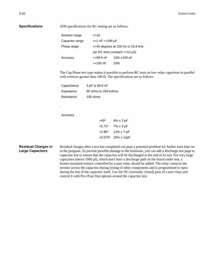
3-20 CAPACITORS
arallel
later on page to large
e n
Specifications ATB specifications for RC testing are as follows:
The Cap Phase test type makes it possible to perform RC tests on low value capacitors in pwith resistors greater than 100 Ω. The specifications are as follows:
.
Residual Charges in Large Capacitors
Residual charges after a test has completed can pose a potential problem for further tests in the program. To prevent possible damage to the hardware, you can add a discharge testcapacitor test to ensure that the capacitor will be discharged at the end of its test. For verycapacitors (above 1000 µf), which don't have a discharge path on the board under test, a fixture-mounted resistor controlled by a user relay should be added. The relay connects thresistor across the capacitor during testing of other components and is programmed to opeduring the test of the capacitor itself. Use the NC (normally closed) pins of a user relay andcontrol it with Pre-/Post-Test options around the capacitor test.
Resistor range >=10
Capacitor range >=1 nF <=299 µF
Phase angle >=45 degrees at 159 Hz or 15.9 kHz
(an RC time constant >=10 µS)
Accuracy <=99.9 nF 10% ±100 pF
>=100 nF 20%
Capacitance 3 pF to 99.9 nF
Impedance 90 ohms to 250 kohms
Resistance 100 ohms
Accuracy
>45º 6% ± 3 pF
>5.71º 7% ± 5 pF
>2.86º 12% ± 7 pF
>0.573º 25% ± 12pF

3-21
Stim I. th
of the
red
Longhand Capacitor Tests
Although not recommended, capacitor test can be done with the longhand test type Test V Test I Stim V mode is not suitable because of the inherent stability problems associated wicapacitors placed in the input leg of the measurement amplifier.
ProgrammingTo program a capacitor test in TVSI mode, you need to calculate the expected impedancecomponent using the following formula.
where Pi = 3.14159 F = stimulus frequency in Hz C = capacitance in Farad Xc = impedance in OhmsOr abbreviated as
where Omega AC1 = 1000 Omega AC2 = 10000 Omega AC3 = 100000 C = capacitance in Farads Xc = impedance in Ohms
Then calculate the stimulus current to yield a certain test voltage according to Ohms law.
where Istim = peak stimulus current in Amperes V_dut = peak stimulus voltage in Volts Xc = impedance in Ohms
Note that the expected V_dut is a peak value that needs to be multiplied by 2 when measuwith Pk-Pk measure type.
For example:
For a 1nF capacitor the impedance when measured with AC2 is
Xc1
2 Pi F C⋅ ⋅ ⋅------------------------------=
Xc1
Omega C⋅---------------------------=
IstimV_dut expected
Xc expected-------------------------------------=
Xc1
10000 1nF⋅------------------------------ 100KΩ==
Istim100mV100KΩ------------------ 1uA peak( )==
Z1800-Series Component Test Reference

3-22 CAPACITORS
hand
ect for he same
Longhand Test Properties pageThe longhand Test Properties page should then be setup as follows:
• Stim: 1 uA AC2
• Measure: (100mv * 2) ± tol, measure type Pk-Pk
Wait times . Be aware that wait times need to be kept short when you test capacitors in longmode. Long wait times can adversely affect the result.
Since longhand tests are not specific to the component under test, the system cannot correrrors and parasitic values that makes longhand tests less precise than shorthand test for tcomponent.
18xx Windows mode-init_com
Page 1 of 1
Test Data
Controls
Test Type: Capacitor
Edit Options Tools Revert Validate QuitSave
Component Properties
Test Properties Options Indicators
Pre Post CntrlCurrent Page
START CANCEL SOF HLD RPT CRTC:/TPD/KMAR1 - ICT
Wire Mode: 3 Precise: Off Highguard: Off Averaging: 1Guard Mode: ActiveFast Mode: Off
ScaleHighLowMeasure Type : Pk-Pk
mv220180
StimulusMeasureReferenceWait (ms)Squelch (ms)
:::
:::::
Pin 1 (42)Pin 2 (68)
00
Stim Value (ma)ScaleStim Type
:::
1uaAC 2
Test Type: Test V Stim I Extended: Off

3-23
t to
Conversion . To automatically convert a shorthand test into a longhand test, use the ConverLonghand selection from the Tools pull-down menu while Test Properties for a particular shorthand capacitor is displayed.AC1 AC2 AC3 AC1 AC2 AC3
10 PF 1.00E+08Ω 1E+07Ω 1.00E+06Ω 10 NF 100000.00Ω 10000.00Ω 1000.00Ω
18 PF 5.56E+07 5.56E+06 5.56E+05 18 NF 55555.56 5555.56 555.56
22 PF 4.55E+07 4.55E+06 4.55E+05 22 NF 45454.55 4545.45 454.55
27 PF 3.70E+07 3.70E+06 3.70E+05 27 NF 37037.04 3703.70 370.37
33 PF 3.03E+07 3.03E+06 3.03E+05 33 NF 30303.03 3030.30 303.03
39 PF 2.56E+07 2.56E+06 2.56E+05 39 NF 25641.03 2564.10 256.41
47 PF 2.13E+07 2.13E+06 2.13E+05 47 NF 21276.60 2127.66 212.77
56 PF 1.79E+07 1.79E+06 1.79E+05 56 NF 17857.14 1785.71 178.57
68 PF 1.47E+07 1.47E+06 1.47E+05 68 NF 14705.88 1470.59 147.06
82 PF 1.22E+07 1.22E+06 1.22E+05 82 NF 12195.12 1219.51 121.95
100 PF 1.00E+07 1000000 100000 100 NF 10000.00 1000.00 100.00
180 PF 5.56E+06 5.56E+05 55555.56 180 NF 5555.56 555.56 55.56
220 PF 4.55E+06 4.55E+05 45454.55 220 NF 4545.45 454.55 45.45
270 PF 3.70E+06 3.70E+05 37037.04 270 NF 3703.70 370.37 37.04
330 PF 3.03E+06 3.03E+05 30303.03 330 NF 3030.30 303.03 30.30
390 PF 2.56E+06 2.56E+05 25641.03 390 NF 2564.10 256.41 25.64
470 PF 2.13E+06 2.13E+05 21276.60 470 NF 2127.66 212.77 21.28
560 PF 1.79E+06 1.79E+05 17857.14 560 NF 1785.71 178.57 17.86
680 PF 1.47E+06 1.47E+05 14705.88 680 NF 1470.59 147.06 14.71
820 PF 1.22E+06 1.22E+05 12195.12 820 NF 1219.51 121.95 12.20
1 NF 1.00E+06 100000 10000.00 1 UF 1000.00 100.00 10.00
1.8 NF 5.56E+05 55555.56 5555.56 1.8 UF 555.56 55.56 5.56
2.2 NF 4.55E+05 45454.55 4545.45 2.2 UF 454.55 45.45 4.55
2.7 NF 3.70E+05 37037.04 3703.70 2.7 UF 370.37 37.04 3.70
3.3 NF 3.03E+05 30303.03 3030.30 3.3 UF 303.03 30.30 3.03
3.9 NF 2.56E+05 25641.03 2564.10 3.9 UF 256.41 25.64 2.56
4.7 NF 2.13E+05 21276.60 2127.66 4.7 UF 212.77 21.28 2.13
5.6 NF 1.79E+05 17857.14 1785.71 5.6 UF 178.57 17.86 1.79
6.8 NF 1.47E+05 14705.88 1470.59 6.8 UF 147.06 14.71 1.47
8.2 NF 1.22E+05 12195.12 1219.51 8.2 UF 121.95 12.20 1.22
Z1800-Series Component Test Reference

your g
ls that e
e uli
ray
s o ereby
I,
e
4 DIGITAL DEVICES
If you have an analog-only test system, information regarding digital test is not pertinent totest situation. The analog-only functionality prevents you from generating, editing, or runnindigital tests.
Gray Code and Vector Overview
Generally, a digital IC test applies logic signals to a device's inputs and analyzes the signaappear on the outputs. The applied logic signals are either Gray code stimuli or vectors. Thresults of the Gray code stimuli on the outputs are analyzed (measured) with three possibldigital measurement methods: CRC, Count, and High. The results of the vector pattern stimare measured by a comparison to known-good patterns.
Gray code frequencies are effective digital stimuli for testing
• SSI and MSI devices
• PALs where test patterns are unavailable
• RAMs and ROMs, all addresses are generated and all cells checked
• some LSI devices where the need for programming is limited
Using Gray code to test a device with large numbers of inputs becomes difficult because Gcode has only 14 unique stimuli.
Vector patterns are effective for complex pattern sets where no regular or coherent stimulupatterns exist, and for sampling digital responses where each bit is individually compared tknown-good data. Tester-per-pin architecture provides a unique driver behind every pin, thallowing stimulus by random patterns.
Vectors are effective digital stimuli and response patterns for testing PALs, ASICs, LSI, VLSand boundary scan devices.
Digital Test Properties for Gray code and vector tests, explained later in this section, providfields to specify the digital stimulus and measurement requirements.
Refer to the Z1800-Series Programmer’s Guidebook , Chapter 5, for information about guardsand disables and for further background information regarding digital test philosophy.
Digital Test Specifications
Non-Multiplexed StimulusEvery pin has a unique driver zand receiver.
• Every driver is capable of providing both Gray code and vector stimulus
• Fixed +5 Volt Driver Reference
Voh(max) = +4.5V, no load
Voh = +3.0V, Ioh = 350 mA
Vol(min) = +0.2V, no load
Vol= +0.8V, Iol = 200 mA
• Slew Rate:
120V/us, no load
100V/us, 90 ohm load
150v/us, Rise, 1 Kohm || 100 pF
160v/us, Fall, 1 Kohm || 100 pF
4-2 DIGITAL DEVICES
%
est
having
V e eds
e burst
V, or
cified
Programmable Measurement Threshold Reference
• Threshold reference can be programmed -2 V to +9.95 V. Accuracy of programming is 1±35 mV.
• Can select comparison to dual or single threshold.
• Programmed threshold levels and type (dual or single) apply to all measurements in a tstep.
Driver/Receiver Boards—Digital MeasurementDriver/receiver boards are organized for digital measurement in two sections, each section a 16:3 matrix.
Programming features of the boards are as follows:
• Threshold comparison at driver/receiver board
• Receiver Specs:
Threshold detection accuracy: Threshold reference ± 200 mV
The receiver will transition from one state to the other if the input signal is more than 200 mfrom the threshold reference cited above. For example, if receiver output is logic low and ththreshold reference is 1.0 V, receiver output will go to logic high when the input signal exce1.2 V.
• Acceptable voltage range going into the receiver without damaging the tester:
-10V to +10V, response only pin
0V to +5V, stim and response pin
• Open receiver input defaults to Logic High Input Resistance:
4 Kohm, minimum
• Single threshold, digital only tests:
Minimum 3 measurements/burst
Maximum 6 measurements/burst
• Dual threshold, digital only tests:
Maximum 3 measurements/burst
• Mixed mode: analog measurement reduces possible digital measurements by one for thin which analog measurement is taken.
• Mixed mode: analog stimulus reduces possible digital measurements by one for all measurements in group.
• Software automatically assigns measurement pins to matrix, no special fixture wiring required.
Termination Resistors
• Provide loads to measurement nodes
• Choices: 1K and 500 Ohms to +5V, Prog 5.5 V, or ground, or 1K each to +5 V, Prog 5.5ground
• Adds ~500 pF to measurement node when selected
• Default: No terminators selected
Software Features
• Software can automatically learn response from DUT
• Software Timeout: The software timeout notifies the user if a burst will exceed user-spebackdrive timeout and will not run the burst. Default: No timeout

4-3
cy
ents
Duty Cycle Control
• Allows user to specify maximum duty cycle of backdrive in a test program.
• Default = 0 (Run at maximum speed, no enforced cool-off)
• Percent specified = backdrive time/off-time & backdrive time
Gray Code Tests Refer to the table below for a description of Gray code's significant characteristics.
Specifications Measurement types:
• Signature Analysis (CRC) up to 2 MHz
Hicheck, if selected, identifies stuck high pins.
• Transition Counting (COUNT) up to 5 MHz
• Duty Cycle (HIGH) up to 2 MHz
• One COUNT or HIGH measurement per burst
• COUNT and HIGH always run in separate bursts.
Measurement enable timing:
• Specified per measurement pin
• All pins in a burst have same enable timing
• Programmed in reference to Gray code frequencies:
FROM—Specifies when measurements begin, Default F1.
TO—Specifies when burst ends, Default: F(N+2),where FN is highest stimulus frequenprogrammed.
WHILE—Allows specifying up to 2 frequencies that must be true in order for measuremto be enabled.
Default—always
Pattern Depth: 1 k pin memory
Property Description
Clock ticks All generators clocked from a common source, and move in lockstep with one another, producing identical stimulus timing relationships each time a burst runs.
Common timing origin All edges related to timing origin, one clock tick before first edge of F1.
No simultaneous transitions
At each clock tick, one and only one stimulus channel changes state. Thus small timing-skew changes from pin to pin cannot significantly affect test results (no-race conditions). Also, since signals are static most of the time, and one signal changes at a time, crosstalk and noise are minimal.
Double coverage bursts A burst of F1, F2, and F3 signals would (in the default case) terminate at the rising edge of F5, having twice attained each of the 8 possible states.
Repeatable logic path Ensures that each board receives the same, repeatable test.
Easily visible markers For triggering oscilloscopes or logic analyzers while debugging. (Test window and measurement window.)
Z1800-Series Component Test Reference

4-4 DIGITAL DEVICES
ging
*), be with
Device Size Constraints:
• Disables: 128 nodes maximum
• Device pins in test: 128 maximum
• Guards per test: 20 maximum
Programmable clock rate
• Clock Frequency = 2MHz/CD, where CD= Clock Divisor) 1 <= CD <= 200
• Default and Maximum Frequency: 2MHz (CD =1)
• Minimum Frequency: 10 KHz (CD = 200)
• Single clock for stim and measure
Hardware time-out: <= 16 ms @ 2 MHzHardware timeout is at F16 <= 16 ms @ 2 MHz. It increases proportionately with the chanclock divisor. For example, when CD = 2, timeout is 32 ms.
Mixed mode: Analog stimulus and measurement within digital test.
• Up to 10 analog pins per test step (device)
• Single analog stimulus in each group
• Single analog measurement per burst
• Software ensures that analog measurement falls within digital burst
Gray Code Stimulus Up to 14 Gray code frequencies (F1 through F14) and their complements (F1* through F14preset high (PH), preset low (PL), preset pulse (PP), logic high (LH), and logic low (LL) canapplied to the device-under-test in any combination. Preset pulse works only in conjunctionthe programmed frequency. Connect and disconnect features also provide synchronous three-state function.
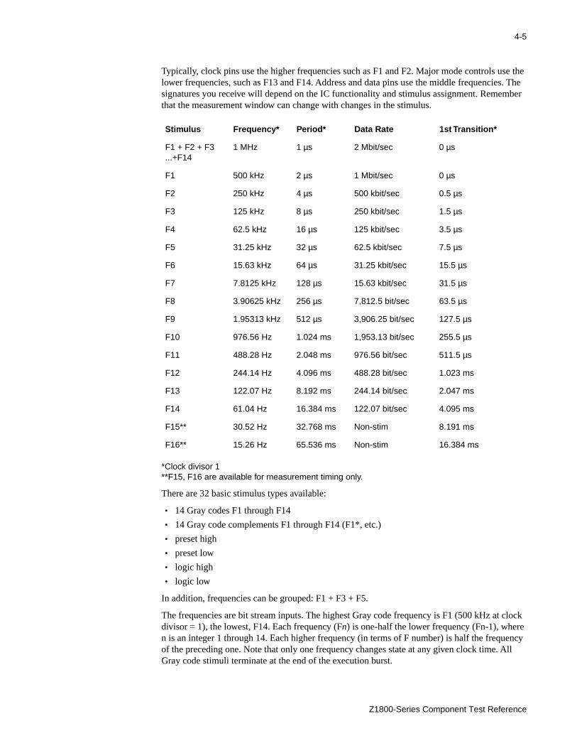
4-5
se the s. The
mber
clock ency All
Typically, clock pins use the higher frequencies such as F1 and F2. Major mode controls ulower frequencies, such as F13 and F14. Address and data pins use the middle frequenciesignatures you receive will depend on the IC functionality and stimulus assignment. Remethat the measurement window can change with changes in the stimulus.
*Clock divisor 1**F15, F16 are available for measurement timing only.
There are 32 basic stimulus types available:
• 14 Gray codes F1 through F14
• 14 Gray code complements F1 through F14 (F1*, etc.)
• preset high
• preset low
• logic high
• logic low
In addition, frequencies can be grouped: F1 + F3 + F5.
The frequencies are bit stream inputs. The highest Gray code frequency is F1 (500 kHz atdivisor = 1), the lowest, F14. Each frequency (Fn) is one-half the lower frequency (Fn-1), wheren is an integer 1 through 14. Each higher frequency (in terms of F number) is half the frequof the preceding one. Note that only one frequency changes state at any given clock time. Gray code stimuli terminate at the end of the execution burst.
Stimulus Frequency* Period* Data Rate 1st Transition*
F1 + F2 + F3 ...+F14
1 MHz 1 µs 2 Mbit/sec 0 µs
F1 500 kHz 2 µs 1 Mbit/sec 0 µs
F2 250 kHz 4 µs 500 kbit/sec 0.5 µs
F3 125 kHz 8 µs 250 kbit/sec 1.5 µs
F4 62.5 kHz 16 µs 125 kbit/sec 3.5 µs
F5 31.25 kHz 32 µs 62.5 kbit/sec 7.5 µs
F6 15.63 kHz 64 µs 31.25 kbit/sec 15.5 µs
F7 7.8125 kHz 128 µs 15.63 kbit/sec 31.5 µs
F8 3.90625 kHz 256 µs 7,812.5 bit/sec 63.5 µs
F9 1.95313 kHz 512 µs 3,906.25 bit/sec 127.5 µs
F10 976.56 Hz 1.024 ms 1,953.13 bit/sec 255.5 µs
F11 488.28 Hz 2.048 ms 976.56 bit/sec 511.5 µs
F12 244.14 Hz 4.096 ms 488.28 bit/sec 1.023 ms
F13 122.07 Hz 8.192 ms 244.14 bit/sec 2.047 ms
F14 61.04 Hz 16.384 ms 122.07 bit/sec 4.095 ms
F15** 30.52 Hz 32.768 ms Non-stim 8.191 ms
F16** 15.26 Hz 65.536 ms Non-stim 16.384 ms
Z1800-Series Component Test Reference

4-6 DIGITAL DEVICES
re
ted
o, the
The following illustration shows the 32 basic discrete Gray code inputs.
Gray-code digital waveforms (32 in all, including complements)
Each of the tester’s channels has its own individual Gray-code generator. The generators apowerful, flexible, and easily programmed. The signature generators, which evaluate the behavior of ICs on the DUT, measure during an interval known as the listen window. Selecedges corresponding to the Gray-code set open, close, and gate the listen window.
You can use Gray code in debug mode to validate that stimuli are stable by checking that achange in each input pin’s stimulus also changes at least one of the output signatures. Alssignature should not change when you change the clock rate.
F1
F2
F3
F4
F14
Gray Code FrequenciesT=0
Presets
Levels(Hi, Lo)
Preset Pulse (PP)(Hi, Lo)
(Any frequency F1 through F14)Preset PulseEquivalent to PH + F1
LH
LL
NOTE: The inverted F1-F14 frequencies are also availble (F1*-F14*).
PLPH

4-7
will
iming ncies
When you edit the Stim Type and Stimulus Frequencies in the Digital Stimulus window, youaffect the overall measurement window timing. It is important to note, however, that if you change the Stimulus Type from Freq to another type such as LL or PH, the measurement twill remain the same unless you deselect any frequencies enabled in the Stimulus Frequearea before changing the Stim Type.
Digital StimulusStim Type : Freq
F1( )
F2( )
F3( )
F4( )
F5( )
F6( )
F7( )
F8( )
F9( )
F10( )
F11( )
F12( )
F13( )
F14( )
Comp( )
Connect/Disconnect Continous
PHPLLLLHFreqPP
18xx Windows mode-init_com
Edit Options Tools Revert Validate QuitSave
Component Properties
Worksheet Options Indicators
Pre Post Cntrl
START CANCEL SOF HLD RPT CRT
Number of Pins: 20
+ID: Name: Desc:
Device Type:
D203 74lS240 D203 74HC04
Gray Code
Low ThresholdHigh ThresholdClock DivisorLogic LevelTerminator
:::::
1.61.615V5ØØ O Pull-Up
Test Type: Gray Code
12345
F2
F2
F2
CRC 78A7
CRC 78A7
CRC 78A7
Pin109876
PinStimulus Measure
F2
F2
CRC 78A7
CRC 78A7
CRC 78A7
Stimulus Measure
C:\TPD\DEMO - ICT
Z1800-Series Component Test Reference
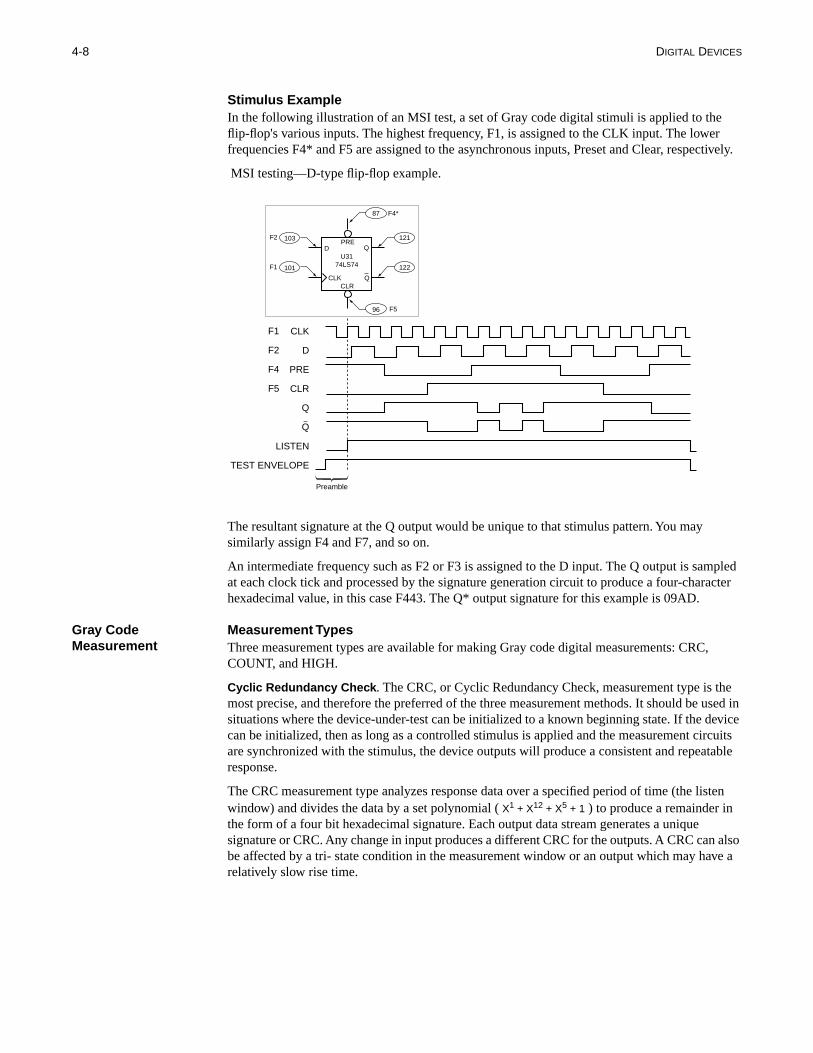
4-8 DIGITAL DEVICES
r
ctively.
mpled acter
,
he used in evice
rcuits table
isten
n also ve a
Stimulus ExampleIn the following illustration of an MSI test, a set of Gray code digital stimuli is applied to theflip-flop's various inputs. The highest frequency, F1, is assigned to the CLK input. The lowefrequencies F4* and F5 are assigned to the asynchronous inputs, Preset and Clear, respe
MSI testing—D-type flip-flop example.
The resultant signature at the Q output would be unique to that stimulus pattern. You may similarly assign F4 and F7, and so on.
An intermediate frequency such as F2 or F3 is assigned to the D input. The Q output is saat each clock tick and processed by the signature generation circuit to produce a four-charhexadecimal value, in this case F443. The Q* output signature for this example is 09AD.
Gray Code Measurement
Measurement TypesThree measurement types are available for making Gray code digital measurements: CRCCOUNT, and HIGH.
Cyclic Redundancy Check . The CRC, or Cyclic Redundancy Check, measurement type is tmost precise, and therefore the preferred of the three measurement methods. It should besituations where the device-under-test can be initialized to a known beginning state. If the dcan be initialized, then as long as a controlled stimulus is applied and the measurement ciare synchronized with the stimulus, the device outputs will produce a consistent and repearesponse.
The CRC measurement type analyzes response data over a specified period of time (the lwindow) and divides the data by a set polynomial ( X1 + X12 + X5 + 1 ) to produce a remainder in the form of a four bit hexadecimal signature. Each output data stream generates a unique signature or CRC. Any change in input produces a different CRC for the outputs. A CRC cabe affected by a tri- state condition in the measurement window or an output which may harelatively slow rise time.
CLK
D
PRE
CLR
Q
Q
LISTEN
TEST ENVELOPE
Preamble
PRE
87
103
101
CLR
D
CLK
Q
Q
U3174LS74
121
122
F2
F1
F4*
96 F5
F1
F2
F4
F5

4-9
down tate. weak p to
h the cimal
5 .
tiple one be t type lue for eed
ile the umber
ount ized or ivisor
KHz
bove fault
t cy
rement e rther oints.
Measurements on tri-stated outputs should be avoided, or if unavoidable, a pull-up or pull should be programmed to ensure that the measured output always tri-states to the same sOpen collector devices may have slow rise times if they are heavily loaded or if they have apull-up. Clock these tests down or program an additional pull-up to ensure a stable CRC. Usix CRC measurements can be made per digital burst. The actual number depends on:
• wiring configuration
• Hicheck usage
• group considerations
• threshold types
• mixed mode usage
• differences in the listen window
Count . The Count measurement type counts the number of positive-going transitions througprogrammed threshold during the measurement window and displays them as a five-digit denumber. The maximum display for the count function is 65535 which corresponds to 6.553MHz. The Count clock is 8 MHz, so measuring frequencies above 5 MHz is not practicableCounting more than 65535 transitions in one window will result in counter circuit overflow. Counting 65537 transitions will display a count of 00002 or two counts beyond 65535. Mulsimultaneous Count measurements are not possible because the THC or VP contains onlycount circuit. The count measurement method is useful when the device-under-test cannotinitialized and the beginning state of the device is unknown. Since the Count measuremenis used on devices that cannot be initialized, a measurement range rather than a single vashould be programmed. The TO range specifier in the Digital Measure window is providedthis purpose. Free-running clocks and counters are prime examples of devices which will nthe count measurement type.
High . The High measurement type counts the number of master clock pulses that occur whmeasurement node is at a logic high state. The result is displayed as a five-digit decimal nwith an upper limit of 32767 (2 MHz master clock counted out to F16 or for 16.384 ms). Multiple simultaneous High measurements are not possible for the same reasons as the Cmeasurement type. The high measurement type is useful when the device cannot be initialif the duty cycle of the device is the desired measurement parameter. One-shots are primeexamples of devices which are best tested with the High measurement type. Using Clock Dmultiples of two on a High measurement will result in measurement data that directly corresponds to the device time-out. Use master clock frequencies of 1MHz (Clock 2) or 100(Clock 20) or 10KHz (Clock 200) for direct measurement data correlation.
Measurement WindowsCare should be taken when programming FROM, TO, WHILE 1, WHILE 2 parameters. Unexpected measurement windows may be generated if invalid arguments are chosen.
Whenever Gray code stimuli are programmed, and a node is measured using one of the ameasurements types, the system software creates a default measurement window. The demeasurement window starts just after the first transition of F1 and ends just before the firstransition of the frequency, which is two frequencies beyond the highest numbered frequenprogrammed. For example, if the highest stimulus frequency used is F4, the default measuwindow begins on the first transition of F1 and ends just before the first transition of F6. Thdefault measurement window can be modified to start and stop at selected intervals and fumodified to make measurements only at selected times within the selected start and stop p
Z1800-Series Component Test Reference

4-10 DIGITAL DEVICES
ld the F8
lized OM
Valid re d
e
ts are l
while
dds mp was
-level
e ry ment
utput tterns
ates the iting a reads ment
the t ncies
s low a lower
The Digital Measure parameters that accomplish these modifications are:
• From
• To
• While 1
• While 2
FROM. The FROM measurement modifier indicates where the measurement window shouopen. Valid arguments to the From parameter are F1 through F15. Choosing FROM: F8 inDigital Measure window would program a digital measurement window that starts just aftergoes high and ends just before F10 goes high. The FROM parameter is useful when the device-under-test requires time to reach a known state. Shift registers that cannot be initiaand outputs that have very slow rise times are prime examples of devices that need the FRmeasurement modifier.
TO. The TO measurement modifier indicates where the measurement window should end.arguments to the TO parameter are F2 through F16. Choosing TO: F8 in the Digital Measuwindow would program a digital measurement window that starts just after F1 goes high anends just before F8 goes high.
WHILE 1. The WHILE 1 measurement modifier indicates that measurements should only bmade while the programmed frequency is true within the FROM TO range window. Valid arguments to the From parameter are F1 through F14. The compliments of these argumenalso available. Choosing While 1: F5 in the Digital Measure window would program a digitameasurement window that starts just after the programmed FROM point and samples onlyF5 is high until just before the programmed TO point goes high.
WHILE 2. The WHILE 2 measurement modifier is an extension to the WHILE 1 modifier. It aa second while parameter to the programmed From-To window. Choosing WHILE 2: F7 Co(V) to the above While 1 example would create a Listen window that sampled only while F5high and F7 was low.
Using Gray Code to Test Memory Devices
Memory tests using Gray code stimulus and signature analysis methods provide 100% pinfault coverage for most devices.Gray code is engineered in such a way that if you assign adifferent frequency to each input, when you measure a device to the default measurementwindow, you automatically realize all the input states for that device.
Use a group of Gray code frequencies to produce all possible address combinations on thaddress bus inputs of ROMs, for example. Gray codes or static levels provide the necessacontrol input signals, like chip select and output enable. A CRC (signature) type of measureon each data output pin collects the long streams of output data. The CRC for each data opin uniquely represents the exact data pattern that results from the Gray code stimulus paapplied at the device input pins.
An SRAM test can also employ Gray code frequencies to write data into the device beforereading out its contents. Generally, a frequency lower than those on the address lines operRead/Write* line. The lower-numbered frequency covers the entire address space while wrdata pattern into the SRAM. The Read/Write* line transitions before the same addressing back the contents. The Read/Write* line's stimulus frequency can also control the measureinterval (window) and sample only the read data.
Unlike SRAM tests, DRAM tests require refresh operations (RAS/CAS cycles). To achieveRAS/CAS operation, use two Gray code frequencies to generate the two signals. The moscommon arrangement is to use an inverted F1 (F1*) for CAS and F2 for RAS. These frequeprovide the most common RAS/CAS relationship where the RAS signal goes low, CAS goethen high, and RAS returns high. If RAS and CAS are F1 and F2, the address bus must be (high-numbered) frequency.

4-11
and
for
the
hey
e Step
Vector Tests Vector stimulus allows specifying drive high, drive low, or high impedance state for each pinfor each clock cycle.
Vector measurement allows specifying expect high, expect low, or ignore for each pin and each clock cycle.
Specifications Measurement enable timing
• Vector Enable specifies each pin at each clock cycle independently.
• Global Ignore specifies that all measure pins are ignored on a given clock cycle.
Pattern Depth:
• Vector Processor board contains 1 Mbyte VP1, or 4 Mbyte VP3, of memory, with 64K reserved for use by its microprocessor.
• Remaining memory is available for test patterns.
• Memory consumption is pattern-dependent.
• Each clock cycle consumes at least 4 bytes.
• No maximum pattern depth is enforced, and 100K patterns (clock cycles) should be achievable.
Device Size Constraints:
• No device size constraints are enforced, other than those of tester hardware:
Maximum nodes = 2048 for 1820, 1860, 1890, and 1888-2
= 640 for 1800, 1840, 1880, and 1888-1
• Disable nodes:
Quantity limited only by tester hardware. Duplicate nodes produce an error message.
Disables can be any series of vectors, and are applied prior to the patterns specified indigital Test Properties.
Both Gray code and vector disables are run before all digital tests. The order in which tare run depends on the type of test you are executing. Refer also to the Z1800-Series Programmer’s Guidebook , Chapter 5.
Disable nodes hold their last state during the test page burst.
• Guard nodes:
Quantity limited only by tester hardware.
Guard nodes are specified as additional nodes in the digital Test Properties portion of thWorksheet.
Programmable clock rate
• Separate clocks for stimulus and measurement.
• The stimulus clock reference is free-running.
• The period of the stimulus clock reference is programmable for each test step.
Programming resolution: 25 ns
Clock Divisor (CD): 20 <= CD <= 32767
Default and minimum period: 500 ns (CD=20)
• Multiple stimulus clock reference periods may elapse between stimulus clocks (i.e. the stimulus clock period is irregular, but synchronous to the reference).
• All stimulus pin changes are synchronous with the stimulus clock.
Z1800-Series Component Test Reference

4-12 DIGITAL DEVICES
clock.
tests te t in for ely etitive, ly ripheral easily
alent. can be p in have
est.
evices r P mory great ry is actual is st. The
the d Scan
ata to After d gular
s. l suited
• For a test step, all measurements are taken the same amount of time after the stimulus
• The measurement delay is programmable.
Programming resolution: 25 ns
Measurement Delay (MD): 4 <= MD <= CD
Default period: 500 ns (MD=20)
Minimum period: 100 ns (MD=4)
Measurement delay cannot exceed stimulus clock reference period.
Vector Test Methods Z1800-series testers with the Vector Performance option are capable of performing vector on digital devices. While Gray code testing allows for easy-to-understand and easy-to-creaprograms, vector testing provides great flexibility in specifying the test pattern. A vector tespattern specifies the state of each stimulus pin and the expected state of each response pevery clock cycle of the pattern. Since each pin is uniquely specified, its pattern is completindependent from the other pins. Whereas Gray code test patterns are predictable and repvector test patterns can vary greatly, from extremely repetitive, like a clock pin, to completerandom, like a serial data stream. Devices such as microprocessors and programmable pedevices have read and write cycles that cannot readily be created with Gray code, but are managed with vector test patterns.
Vector testing is useful not only because it is flexible, but also because its usage is so prevCustom devices such as ASICs are typically tested by vector test patterns. These patternstranslated into a format that the Z1800-series testers can use, allowing board test a step ucreating a test for those devices. Similarly, programmable devices such as PALs frequentlyJEDEC format test vectors. The Z1800-series can take in these patterns for use in board t
Vector Processor Controller BoardThe Vector Performance option is required on Z1800-series testers in order to test digital dusing vectors. The heart of the Vector Performance option is the Vector Processor controlleboard (VP). The VP employs a unique patented approach in performing vector tests. The Vapproach maximizes memory efficiency. The efficiency is realized in several ways. First, meis centralized. All memory resides on the VP controller; there is no pin memory. Vectors of length can be created since lengths are not constrained by per pin memory. Until all memoused up, more vectors can be stored. Next, the memories store pin transitions, rather thanpin states, thus reducing the amount of memory required to store a vector. Finally, memoryreused. Each clock cycle has a set of pins associated with it. The set of pins is stored in a lilist is stored only once, but multiple clocks (states) can use it.
The VP is very efficient at applying deep vector patterns. The VP supports vector test usingsame driver/receiver boards used in a standard Z1800-series tester for Gray code tests anrequires no special fixture considerations. Its capacity for long vectors supports Boundary and deep memory testing.
Vector Clock—Priming PinsWhen running a digital test burst, the VP accesses its centralized memory and uses that daddress and prime pins one at a time. Priming notifies a pin that is about to change state. priming all pins, the VP issues the vector clock, causing all primed pins to change state anclearing all primes. One effect of serially addressing pins is that the pattern changes at irreintervals. If many pins must change on a clock cycle, all of those pins must be addressed individually and primed for change. Priming applies to both stimulus and measurement pinPriming of a measurement pin indicates a change in expected data. The architecture is welfor testing static gate arrays and other devices insensitive to clock rate.

4-13
ed , but e all
, the two ional few us), so
als es.
eiver
the
test can igital ach
have ation
ted es
s of a rom akes
t ading te ween
d fter last gh the ected. logic
or and
The vector clock is synchronized to a master clock (default frequency is 2 MHz) and is issuonly after all active pins are primed. The vector clock always occurs at a master clock edgeconsecutive vector clocks may occur after multiple master clocks. The time required to primpins is proportional to the number of pins changing state. The more pins that change statelonger it takes to prime them, resulting in irregular clock intervals. The VP can prime up to pins within the 500 ns (default) clock period. Each additional prime takes 150 ns with addittime added as needed for synchronization to the master clock. Most test patterns change apins on each clock cycle, and infrequently change many pins (usually an address or data bthat the pattern rate will average out about 1 MHz (half the default clock rate).
Digital Response SignalsZ1800-series testers support six simultaneous digital measurements. Digital response signtravel from the driver/receiver boards to the controller board through six digital response linThe controller captures and processes the digital response signals.
On the VP controller, each digital response line has a prime circuit like that on the driver/recboard. For vector tests, expected responses are stored in memory, along with the stimuli. Transitions in the expected response are primed like stimulus nodes and change state on stimulus clock.
The tester has only six digital response lines, but can have as many as 2048 pins. A vector expect data on all 2048 pins, at least in theory. All vector tests that require more than six dmeasurements run multiple bursts automatically in order to capture all of the results. For evector test burst, a map memory assigns response pins to the six digital response lines.
Map MemoryEach location in the map memory corresponds to a unique tester pin. Since the tester can2048 pins, the map memory has 2048 locations. The data stored in each map memory locdetermines if the corresponding pin is active for the present burst, and if active, the digital response line on which the pin data is expected. If a response pin is active, then the expecresponse for the appropriate digital line is primed. If a response pin is inactive, then no primoccur.
The contents of the central memory used for priming memory remain constant for all burstgiven vector test; only the map memory is modified for each burst. Two advantages result fthis. First, since the list never changes, each burst of the vector has identical timing. This mtest results repeatable. Next, map memory modification is much simpler and quicker than modifying expect data within the central memory. Reloading the map memory takes at mostwelve write operations: six to clear old assignments, and six to set new assignments. Relocentral memory would take many calculations, and could involve thousands of memory wrioperations. In addition to modifying map memory, response relays are set and cleared betbursts. The time to write the map memory is small compared to relay settling.
Behavior of Disables
When running multiple burst vector tests, the entire stimulus pattern, including disables anguards, runs for each and every burst. Both vector and Gray code disables will hold state atheir disable sequence runs, and until the end of the test pattern burst. For example, if the state of a vector disable sequence programmed the pin high, the pin will remain high throutest pattern burst. For a Gray code disable, logic high, logic low, and presets will act as expIf a disable frequency is programmed, it will act as a logic low for a true frequency, and as ahigh for a complemented frequency.
Be aware that the Disable Table Test Properties function checks for duplicate nodes in vectGray code disable tables. An error message opens if a duplicate node is entered.
Z1800-Series Component Test Reference
4-14 DIGITAL DEVICES
use ith an r, pins iven test, om ate.
clock y is ust
store the ter has er the ailing the
to he ins for
pass e final
due to
les as s
directly . In ding to er
e drive the
Refer to the Z1800-Series Programmer’s Guide , Chapter 5, for more information about Gray code and vectors.
VP Stimulus and Measurement ClocksWhen using the Z1800-series test head controller (Gray code only), stimulus and responsethe same clock. The response from one cycle is recorded at the clock for the next cycle. Wirregular vector clock, test results could be erratic with a single clock. With the VP controllemeasurement capture uses a second clock. The stimulus clock toggles all primed stimulusand expected responses. The measurement clock captures the resulting response. For a gthe measurement clock issues a fixed time after the stimulus clock. This keeps the delay frstimulus to measurement constant throughout test, in spite of the irregular stimulus clock r
The stimulus clock triggers the measurement delay countdown, producing a measurementwith a programmable delay relative to the stimulus clock. The minimum measurement dela100 ns and is programmable in 25 ns increments. The measurement clock for one cycle moccur at or before the next stimulus clock.
Failure RegisterVector tests compare actual and expected response at the measurement clock edge, and result in memory and in a global response failure register. The global response failure regisa failure flag for each digital response line. The failure flag for a response line sets whenevline fails and stays set throughout the burst. This allows the software to quickly determine fpins because it does not have to read the entire response memory. The software retrievesresponse memory contents when displaying results for tests debug and when learning theresponse.
Programming the Listen WindowThe listen window for a response pin can be programmed in two different ways. The first isprogram the individual expect-high, expect-low, and don’t care for the pin for every state. Tother method is to use Global Ignore. Global Ignore acts as a don’t care for all response pclock cycles in which it is programmed. Global Ignore eliminates the need to prime each response pin into a don’t care state. This is especially useful when dealing with buses thatthrough an unknown state. The transitions can all be ignored, and then only the pins whosstate changed need to be primed. Refer to the Z1800-Series Programmer’s Guidebook , Chapter 11, for more information.
Pole Assignments for Vector TestsHoming Loops and Mixed Mode with Vectors make the pole assignment for vector tests complex. In tests with homing loops, it is possible to construct a test which cannot execute a lack of available measurement poles.
All nodes in the 1800-series systems have access to six measurement poles, named Ed, Fd, Gd, Es, Fs, and Gs. The d stands for drive and the s for sense, for historical reasons related to the poused to perform analog Kelvin (that is, four-wire) measurements. For this reason, if a test hmore than six measurement pins, it must be broken up into multiple bursts. All stimulus pinmust, of course, be active during each burst.
Each driver/receiver board in the test head cage serves 32 nodes; the lower 16 nodes canaccess the three drive poles, and the upper 16 have direct access to the three sense polesaddition, there are three bridging relays which can connect any drive pole to the corresponsense pole (for example, the Fd pole to the Fs pole). As a result, all nodes have potential accessall poles. The benefit of this bridging capability is that it often allows more measurements pburst than would otherwise be possible. For example, without bridging, a test having measurements on nodes 0, 1, 2, 32, 33, and 34 would require two bursts, each using all thpoles. However, with bridging, all six nodes can be put into one burst; nodes 0, 1, and 2 on

4-15
ridged iver
ual
three
des.
og hich hich d two
nable is no he
.
).
le test
drive poles and nodes 32, 33, and 34 bridged to the sense poles. Note that nodes can be bonly if the pole being bridged to is not being used by another node on the same driver/receboard.
Dual thresholds also limit the number of nodes that can be measured in a burst. When a dthreshold measure is specified, two complementary poles (for example, Gd and Gs) are assigned to the measured node and the bridging relay between them is closed. Thus, no more than such measurements are possible in a burst.
Analog stimuli and measures affect how poles are assigned to the vector measurement noOnly one analog stimulus is allowed; it is always assigned to the Ed pole and must be present inall bursts. Ten analog measures are allowed (nine if there is an analog stim), and they are assigned to the Fd pole, one per burst.
Finally, there are Homing Loops pins whose corresponding measurement nodes, like analstimuli, must be included in every burst. There is no limit, however, to the number of pins wcan be specified as homing loop pins. As a consequence, it is possible to construct a test wcannot meet all of the above requirements. For example, a test with an analog stimulus, anhoming loop pins, all within the same 16 node group on a driver/receiver board would be uto measure any of the remaining 13 nodes within that node group. If a situation such as thoccurs, an error message will be displayed (if run from the vector editor), which states thatpoles are available to execute this test. You will have to take appropriate action to reduce tdemand for poles.
Digital Test Editing You may edit a digital disable or component test step at any time from the Step Worksheet
To access a digital Step Worksheet from the Main menu, select:
1 The board program
2 Edit
3 Digital
4 Disables or Components (If you select Disables, then choose GC_DIS or VEC_DIS.)5 the digital Step Worksheet from the Component Select window (only for components
The Step Worksheet contains a menu bar, Component Properties, and Test Properties.
Refer to the Z1800-Series Programmer’s Guide , Chapter 3, for an explanation of digital Component Properties.
Digital Test Properties areas (Gray code and vectors) contain the execution data for a singstep.
Z1800-Series Component Test Reference

4-16 DIGITAL DEVICES
in its ode
Gray Code Test Properties
Like analog Test Properties, Gray code Test Properties have a single page which appears entirety when you select a Gray code test. The following illustration shows a typical Gray cStep Worksheet.
18xx Windows mode-init_com
Test Type: Capacitor
Edit Options Tools Revert Validate QuitSave
Component Properties
Test Properties Options Indicators
Pre Post Cntrl
START CANCEL SOF HLD RPT CRT
Test Type: Gray Code
Low ThresholdHigh ThresholdClock DivisorLogic LevelTerminator
:::::
1.61.615V500 O Pull-Up
12345678
LLF2
F3
F4
F5
CRC 9B1F
CRC C492
CRC 3D52
Pin2019181716151413
PinStimulus MeasurePOWERLL
F5
F4
F3
CRC 8AD0
CRC 3D52
CRC C492
Stimulus Measure
+ID: Name: Desc:
Device Type:
U1 (Gray)
Number of Pins: 20
74lS240 Gray Code Simulated test
Gray Code
C:\TPD\DEMO - ICT

4-17
rs.
mber.
Refer to the following table for Gray code Test Properties field details.
The Pin column lists all the device pins. When you select a Pin field, the Pin Record appea
Pin Number is a number of the device package's pin. Node Number is the tester's node nuPin Type lists possible pin functions. Group(s) represent digital burst groupings.
Field Description
Indicators Shows if there are Gray code and/or vector guards. Read only.
Low Threshold Range of -2 to +9.95 Volts. Default is 1.6.
High Threshold Range of -2 to +9.95 Volts. Default is 1.6.
Clock Divisor Governs the clock rate during bursts. The default of 1 provides a 2 MHz master clock;clock divisor 2= 1 MHz; clock divisor 4=500 kHz, and so on.
Terminator Resistive load applied to measurement, usually required for open-collector outputsand for verifying the enable of 3-state devices. Choices are:1K pull-up, 500 Ohm pull-up, 1K pulldown, 500 Ohm pulldown, None, and 1K terminator.Pull-ups are to +5V and pull downs to ground. The 1K terminator has 1K to +5V and 1K to ground.
Logic Level Specifies whether your device is 3 volts or 5 volts. The default is 5 V.
Pin Device pin number. Select to edit Pin Record Menu.
Stimulus Stimulus applied to the device's inputs. Select field to select one of the following:PH, PL, LL, LH, Freq, and PP.
Measure The expected response data for the applicable device output pin. Select from:Measure Type: CRC, COUNT, HIGH Value 1, Range: OR, Single, TOValue 2From, To, While 1 and 2
Pin NumberNode Number Pin TypeGroup(s)
Learn Signature
::::
196S & R1
Pin Record
Z1800-Series Component Test Reference
4-18 DIGITAL DEVICES
single
. gital gic signal
A group is a subset of nodes on an IC package used to test one logical element, such as aNAND gate in a quadruple NAND gate package. Typically, a group describes all inputs andoutputs of a single element. A pin can be assigned to a single group or to multiple groups.
Pin Type offers the pop-up window at left from which you may choose a function for the pinS&R represents digital stimulus and response. Stim D is digital stimulus only. Resp D is diresponse only. Power and Gnd are labels for pins tied to power (logic high) and ground (lolow) sources. NC representsa no pin connection. Tied means that the pin is tied to anotherpin. Stim V (Test Digital Stim Voltage) and Meas V (Test Voltage
Stim Digital) are for mixed mode testing.
Refer to the end of the Digital Test section for further discussion of mixed mode testing.
S&RStim DResp DPowerGndN.C.TiedStimVMeas V
S&R
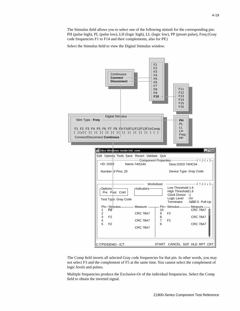
4-19
n: ay
may nt of
p
The Stimulus field allows you to select one of the following stimuli for the corresponding piPH (pulse high), PL (pulse low), LH (logic high), LL (logic low), PP (preset pulse), Freq (Grcode frequencies F1 to F14 and their complements, also for PP.)
Select the Stimulus field to view the Digital Stimulus window.
The Comp field inverts all selected Gray code frequencies for that pin. In other words, younot select F3 and the complement of F5 at the same time. You cannot select the complemelogic levels and pulses.
Multiple frequencies produce the Exclusive-Or of the individual frequencies. Select the Comfield to obtain the inverted signal.
F11F12F13F14F15F16
Digital StimulusStim Type : Freq
F1( )
F2( )
F3( )
F4( )
F5( )
F6( )
F7( )
F8( )
F9( )
F10( )
F11( )
F12( )
F13( )
F14( )
Comp( )
Connect/Disconnect Continous
PHPLLLLHFreqPP
18xx Windows mode-init_com
Edit Options Tools Revert Validate QuitSave
Component Properties
Worksheet Options Indicators
Pre Post Cntrl
START CANCEL SOF HLD RPT CRT
Number of Pins: 20
+ID: Name: Desc:
Device Type:
D203 74lS240 D203 74HC04
Gray Code
Low ThresholdHigh ThresholdClock DivisorLogic LevelTerminator
:::::
1.61.615V5ØØ O Pull-Up
Test Type: Gray Code
12345
F2
F2
F2
CRC 78A7
CRC 78A7
CRC 78A7
Pin109876
PinStimulus Measure
F2
F2
CRC 78A7
CRC 78A7
CRC 78A7
Stimulus Measure
C:\TPD\DEMO - ICT
ContinuousConnectDisconnect
F1F2F3F4F5F6F7F8F9F10
Z1800-Series Component Test Reference

4-20 DIGITAL DEVICES
ates a times .
To, ake ype,
se l.
The Connect/Disconnect field allows you to select one of 16 frequencies. Continuous indiccontinuous, uninterrupted frequency burst. Connect activates the stimulus only during the the qualifier is in the high state. For example, F1 Connect F10 applies F1 when F10 is highDisconnect disables the stimulus only during the times the qualifier is in the high state. Forexample, F1 Disconnect F10 disables F1 when F10 is high.
The Measure field allows you to select Measure Type, Value 1, Range, Value 2, and From,While 1 and 2 with complements. To access the Digital Measure window where you can mthese selections, click the Measure field. Within the Digital Measure window the Measure TRange, and From, To, While1 and While2 fields expand as shown below.
Selecting OR or TO from the Range field enables the Value 2 field.
When you click a From, To, While1 or While2 field, the frequency scroll window appears. Uthe scroll bar to access F11 through F16. Select the Comp field to select the inverted signa
ORSingleTO
Measure TypeValue 1RangeValue 2
FromToWhile 1While 2
::::
::::
DefDefDefDef
Comp ( )Comp ( )
CRC09b1fSingle
Digital MeasureCRCCOUNTHIGH
DefF1F2F3F4F5F6F7F8F910
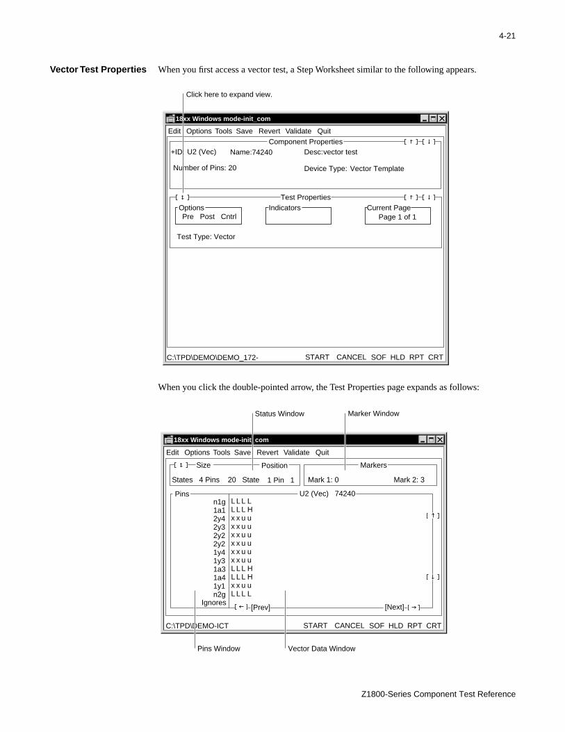
4-21
Vector Test Properties When you first access a vector test, a Step Worksheet similar to the following appears.
When you click the double-pointed arrow, the Test Properties page expands as follows:
18xx Windows mode-init_com
Edit Options Tools Revert Validate Quit
C:\TPD\DEMO\DEMO_172-
Save
Component Properties
Test Properties Options Indicators
Pre Post CntrlCurrent Page
START CANCEL SOF HLD RPT CRT
+ID: Name: Desc:
Device Type:
U2 (Vec)
Number of Pins: 20
74240 vector test
Vector Template
Click here to expand view.
Test Type: Vector
Page 1 of 1
18xx Windows mode-init_com
Edit Options Tools Revert Validate QuitSave
START CANCEL SOF HLD RPT CRT
States 4 Pins 20 State
Size Position
1 Pin 1
Markers
Mark 1: 0 Mark 2: 3
Status Window Marker Window
C:\TPD\DEMO-ICT
Pins
Ignores
n1g1a12y42y32y22y21y41y31a31a41y1n2g
LLxxxxxxLLxL
LLxxxxxxLLxL
LLuuuuuuLLuL
LHuuuuuuHHuL
U2 (Vec) 74240
[Prev] [Next]
Pins Window Vector Data Window
Z1800-Series Component Test Reference

4-22 DIGITAL DEVICES
, lished
disk.
n the r the
rties
r t the of the arker n f the e d
the dow. s
d
ow this n in sert
The Vector Editor is made up of four windows. They are the Status Window, Marker WindowPins Window, and Vector Data Window. Movement between these windows can be accompwith the mouse or the F2 key which changes windows in a counterclockwise order.
Revert . Select Revert at any time to go back to the Test Properties variables last saved on
Status WindowThis window contains the overall dimensions of the vector and the current cursor position iVector Data Window. To go to a particular position in the Vector Data Window you can entecoordinates in the State and Pin fields and either press Enter or click the mouse. The double-arrow field when clicked or Entered will take you back to the compacted Test Propepage.
MarkersMarkers are vertical bars within the Vector Data window. They are there to mark a particulapattern for easy reference. Two markers are supplied. As default these markers come up afirst and last pattern of the vector. To move a marker, just enter the pattern number in one marker fields and press Enter or click. To go to a marker position double-click one of the mfields and the Vector Data window will reposition at that marker if it is not already visible. Aalternate way to move markers is to click and hold the mouse button down on the border oVector Data window directly above a marker. The marker bar will disappear. With the mousbutton still down, drag the mouse to the position that you would like to place the marker anrelease the button. The marker will appear at that position.
Pins WindowThe pin names for each row of the Vector Data window are listed here as well as a row for Ignores. This window scrolls vertically with the movement of the Vector Data window. Also Up, Down, and Enter keys can scroll the Pins window if pressed at the top/bottom of the winThis window’s scrolling is tied with the Vector Data window—if one scrolls vertically, so doethe other.
Clicking or pressing the keypad’s plus key on a field in this window presents the Pin Recorwindow.
Pin Type allows you to specify Unused, Stim, Meas, Stim/Meas, Monitor, Stim V, Meas V, Homing Meas, or Homing S/M.
Pin Name is a 9-character text field for the name of the pin.
With Setup Row Assignments, pins can be moved vertically in the vector editor using the Rand Swap/Insert fields. Initially the row will display the current row of the vector editor that pin resides in. By entering a different number in this field you can change the row of this pithe display. Swap will make this pin trade rows with the pin specified in the row field and Inwill put this pin in the row specified and push all the pins below it down one. This feature isuseful for putting all the pins of a data bus side-by-side on the display.
Pin NumberNode Number Pin TypePin Name
Setup Row Assignments:Row 5: Swap
::::
7214Meas2y2
Pin Record
4-23
oop Pin
a pin so s On.
g a pin
ss
a time. there the
ctor. f its
wn se the
d ta
If a pin type is one in which a response will be taken—Meas, Stim/Meas, Monitor, Homing LMeas, Homing Loop Stim/Meas, Mixed Mode Meas— then other fields will be present in theRecord Menu window.
• Assigned Pole
• Trigger
• Learn Expect Data
The Assigned Pole field indicates the actual measurement pole that has been assigned to that you know where to place your probe on the test jack panel when the Trigger function i
The Trigger field enables you to toggle the Trigger function On and Off. When On, only thevector burst containing this pin will generate a test envelope at the test jack panel. Selectinautomatically deselects any other pin.
Refer to the Z1800-Series Programmer’s Guide , Chapter 11, for more information about usingit to debug vector tests.
The Learn Expect Data field is for learning the measured responses. When you click or preEnter on this field, the data in the Vector Data window for this pin will be replaced with the measured data. This function takes place on a per pin basis—you can learn only one pin atFurthermore, Learn Expect Data is limited to processing 32K of failures in any one pass. Ifis more than 32K’s worth of failures on one pin, you must select Learn again to learn all of data associated with that pin.
Vector Data WindowThe Vector Data window allows you to examine and manipulate the data patterns of the veYou can move in this window by paging or scrolling. Paging moves the window by one half owidth/height, scrolling moves the window by one line. To page vertically use the up and doarrows in the left border or press the Page Up and Page Down keys. To page horizontally, uleft and right arrows in the bottom border or use the key combinations of Ctrl-Left Arrow anCtrl-Right Arrow. To scroll, use the left, right, up, and down arrow keys within the Vector Dawindow.
Z1800-Series Component Test Reference

4-24 DIGITAL DEVICES
by lt state menu
same
can e test
ss, the
When
r of ctor gram tates
he
ed by
r in
ing
roper
You can toggle the state (H, L, Z, u, d, x) of an individual cell within the vector data windowclicking the cell or using the Space bar. See the table below for an explanation of the defaucharacters. You can modify the character set by selecting Modify/Data Characters from thebar. A query window will allow you to edit either hexadecimal or ASCII characters.
If you are working with bidirectional pins, there is no Z state. Because Z and x states are theon Stim/Meas pins, the software allows you to create only an x state on such pins.
The software system cannot instruct you on the best method to correct a bad vector, but itsimplify the process by disclosing failed or unexpected data. When you select Start to run thstep, the software translates, loads, and executes the vector table. If the burst does not pafailures will be highlighted with a defined fail color. The NEXT function lets you advance tonext failing state. The PREV function lets you return to the previous failing state. When youdepress the mouse button on Prev or Next, the cursor highlights the failing vector data cell.you release the mouse button, the cursor control returns to either Prev or Next. Holding themouse button down keeps advancing to the next (or previous) failure.
With the RPT (repeat) function, you can determine if results are stable over a large numberepetitions. The delay function allows you to move a sampling strobe with respect to the veclock signal. With the Learn Expect Data function, you can import test results into a test proand discard the previously programmed results. You are not required to enter any of theseresults—the software will do the work. Note, however, the software will change only those swhich are specified as u or d; it ignores changes to the ignore state.
With SOF (Stop On Fail), you can run a program as an operator. If you choose the editor, tcursor will indicate the first failing bit.
Edit . The Edit command places the cursor in the Vector Data window at the position specifiState/Pin in the Status window.
Save. The Save command briefly issues a message that it is saving the vector test step.
Compress . The Compress command builds a new, compressed internal image of the vectothe form of pointers and lists, and reloads the new pointers and lists into vector processor memory. Editing of vectors creates lists in the vector file that are not referenced any more.Executing Compress after editing will remove these unreferenced lists and run the list sharalgorithm to get maximum use of the list space. Vector compression is not necessary for ptest execution, but when performed, reduces RAM and disk space storage requirements.
When you select Compress, two brief process messages appear.
If you have a slow PC, large vector files will require more time for compression.
State Description
H Drive High
L Drive Low
Z Tristate
u Sense Up
d Sense Down
x Ignore

4-25
ps,
erns. s are
must
the
letes
from
ges, to
Modify . The Modify command allows you to change vector states, guards, pins, homing looand strings and to automatically ignore failing states.
Insert States . Insert States allows you to pad out the overall vector by adding additional pattThe result will be a vector with more states, useful, for example, when additional clock cyclenecessary at a particular point in the test vector. Insert States copies the vector state only immediately prior to insert; it doesn’t give an alternating pattern on the inserted states. Youedit them in.
If new states are being added, a window (Insert States Menu) appears asking at what stateaddition should start and how many states are being added.
Execute the Insert States menu by entering states and selecting Execute.
Cancel aborts the window. The software adds the new, states in the edit fields after issuingprocess messages.
Delete States . Delete States works in much the same way as Insert States, except that it derather than inserts the specified number of test vector states.
Add Guards . Add Guards allows you to add new guard pins. Guard pins isolate the device surrounding devices on the board. The Add Guard window appears.
After you select Execute to add the guard or guards, the software will issue process messathen prompt you to assign a node number or numbers into the window below. Press Enter complete the process.
Insert StatesDelete StatesAdd GuardsRemove GuardsAdd Homing LoopDelete Homing LoopsList Homing LoopsEdit Unused PinsData Characters
Insert States
Add Guards MenuHow many guards to addInitialize to
1Z
EXECUTE CANCEL
::
pin_24 :
Init Guard Nodes
106
Enter Node Number
Z1800-Series Component Test Reference
4-26 DIGITAL DEVICES
es
key
are
t pin or of
ing
e,
Remove Guards . Remove Guards allows you to remove the pins and associated signal namfrom the vector edit window. A deletion window similar to the one below appears when youselect Remove Guards.
Click or press the Space bar on an item to mark the pin/name for deletion. Press the Enterwhen done.
A query window will ask you to confirm deletion. Select Yes to remove the guard. The softwwill then issue process messages and remove the marked guard or guards.
Homing LoopsHoming loops extend board test coverage to include devices that do not have a master resecommand to initialize them to a known state. The homing loop function allows initializationthe device before each section is tested.
To implement the function use the vector editor Modify menu to add, delete and list the homloops.
Add Homing Loop . To add a homing loop to your test program
1 Select the desired vector test from the Component Select window.
2 Click the double-pointed arrow in the left portion of Test Properties to expand the paginvoking the vector editor window.
Pin
check pins to delete
Name
22
23
bd_osc
pin_24

4-27
d end
ned
er the ers
the
rting
3 Define the range for the homing loop by dragging the vertical markers to the start anstates of the desired homing loop, or by entering the desired column numbers in the Markers subwindow at the upper left of the screen.
4 Select Modify/Add Homing Loop.
A query window appears asking you to select OK to create a homing loop that is defiby the area between the two markers. You may also select Cancel.
Homing loops cannot overlap. If Add Homing Loop is selected when the markers eithoverlap or surround existing homing loops, then the homing loops that intersect with newly defined homing loop will be deleted, and the homing loop defined by the markwill be added. This feature can be used to modify existing homing loops simply by repositioning the markers and selecting Add Homing Loops. When you have selectedrange of the homing loop, the area between the markers changes color.
You may select up to 10 homing loops per test.
5 Click OK in the next query window to save your edits.
A Homing Loop window similar to the one below appears.
6 Enter the maximum number of times you want to execute the homing loop before abothe test.
Dra
g M
arke
r
Dra
g M
arke
r
Pins
Ignores
n1g1a12y42y32y22y21y41y31a31a41y1n2g
LLxxxxxxLLxL
LLxxxxxxLLxL
LLuuuuuuLLuL
LHuuuuuuHHuL
U2 (Vec) 74240
[Prev] [Next]
Homing Loops
Enter Maximum Homing Count: 3
Homing Loop 1 Start 1 End 3
(0-65535) Zero is used to disable Homing.
Z1800-Series Component Test Reference

4-28 DIGITAL DEVICES
A
tor ted in
The reen.
e
Delete Homing Loops . To delete homing loops,
1 Select Delete Homing Loops from the Modify menu.
A window appears listing the homing loops you have set up.
2 Click within the parentheses of the homing loop(s) you wish to delete.
The homing loops are deleted when you exit the window.
List Homing Loops . To list homing loops, select List Homing Loops from the Modify menu. list of your selections appears on the screen.
Edit Unused Pin . Edit Unused Pin allows you to assign an active pin type to an unused vecpin. (An unnecessary pin can be marked unused in the pin record. The unused pins are listhe Edit Unused Pin window.)
Select Edit Unused Pin to view and edit the unused pins.
Select the Type field and choose one of the pin types. Select an area outside the window. software will include the former unused pin in the vector edit window when it redraws the sc
Data Characters . Data Characters allows you to select the data characters that represent thvector states.
Homing Loops
Homing Loop Homing LoopHoming Loop
Check Homing Loop(s) to delete.
( )( )( )
123
StartStartStart
EndEndEnd
11832
32032
Pin Name Type
UnusedUnusedUnusedUnusedUnusedUnusedUnusedUnused
gndgndgndgndgndgndgndgnd
4567891011
UnusedStimMeasStim/MeasMonitor
Vector Data Character
Stim HighStim LowTri-StateMeas HighMeas LowDon’t CareAna StimAna No-MeasAna MeasIgnore OffIgnore On
:::::::::::
HLZudxaaM
*
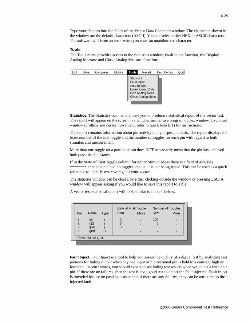
4-29
wn in ers.
st. ntrol
s the
eved
uick
. A
test or lt on a Inject to the
Type your choices into the fields of the Vector Data Character window. The characters shothe window are the default characters (ASCII). You can select either HEX or ASCII charactThe software will issue an error when you enter an unauthorized character.
ToolsThe Tools menu provides access to the Statistics window, Fault Inject function, the DisplayAnalog Measure and Close Analog Measure functions.
Statistics . The Statistics command allows you to produce a statistical report of the vector teThe report will appear on the screen in a window similar to a program output window. To cowindow scrolling and cursor movement, refer to quick help (F1) for instructions.
The report contains information about pin activity on a pin-per-pin basis. The report displayState number of the first toggle and the number of toggles for each pin with regard to bothstimulus and measurement.
More than one toggle on a particular pin does NOT necessarily mean that the pin has achiboth possible data states.
If in the State of First Toggle column for either Stim or Meas there is a field of asterisks ********, then this pin had no toggles, that is, it is not being tested. This can be used as a qreference to identify test coverage of your vector.
The statistics window can be closed by either clicking outside the window or pressing ESCwindow will appear asking if you would like to save this report to a file.
A vector test statistical report will look similar to the one below.
Fault Inject . Fault Inject is a tool to help you assess the quality of a digital test by analyzingpatterns for failing output when any one input or bidirectional pin is held to a constant highlow state. In other words, you should expect to see failing test results when you inject a faupin. If there are no failures, then the test is not a good test to detect the fault injected. Faultis intended for use on passing tests so that if there are any failures, they can be attributed injected fault.
StatisticsFault InjectAuto-IgnoreLearn Expect DataDisp Analog MeasClose Analog Meas
Edit Save Compress Modify Tools Revert Test_Config Quit
Pin Name Type
1234
clkr22Iporgnd
IIIU
State of First ToggleStim Meas
Number of TogglesStim Meas
033-
----
10089-
----
Press ESC to Quit.
Z1800-Series Component Test Reference

4-30 DIGITAL DEVICES
wed want
tailed
care or has rom
ge,
t All,
the
hen
rn only n any ain to
The Fault Inject interface consists of the Fault Inject window listing all the pins you are alloto include in the Fault Inject analysis, their types, and names. You can specify whether youto hold/analyze the pin high, low or both high and low.
When you execute Fault Inject, a report window appears showing the fault coverage and deresults.
Refer to the Z1800-Series Programmer’s Guide , Chapter 11, for detailed information about using Fault Inject.
Auto-Ignore . Auto-Ignore allows you to change all failing states of a vector test to the don’t (X) state. The feature is most useful when a vector test generated by the program generattiming problems. Auto-Ignore automatically changes U and D states to X when the edges fthe template cannot be met by the tester.
To use this tool
1 Select Auto-Ignore from the Modify menu.
A window appears prompting you for a range of pins and vectors to ignore.
2 Specify the range of states.
By default, this range is all of the patterns of the vector. If you want to narrow that ranenter that range in the Auto-Ignore Range field.
3 Select the pins which you wish to have the test mark as ignored.
Either click Select All to specify that you want all failures ignored, or click within the parentheses to select particular measure or stimulus/measure pins. If you click Selecyou can deselect individual pins by clicking the check marks within the parentheses.
4 Click Execute to confirm your selections and execute the test or Cancel to terminate procedure.
Learn Expect Data . The Learn Expect Data field is for learning the measured responses. Wyou click or press Enter on this field, the data in the Vector Data window for this pin will be replaced with the measured data. This function takes place on a per pin basis—you can leaone pin at a time. Furthermore, Learn Expect Data is limited to processing 32K of failures ione pass. If there is more than 32K’s worth of failures on one pin, you must select Learn aglearn all of the data associated with that pin.
Auto-Ignore
Enter State to Start Auto-Ignore at
Auto-Ignore Range is From: 0 To: 3
( )( )( )
Stim/MeasStim/MeasMeas
n1g1a12a3
01
14
Pin Type Name Pin Type Name( )( )
Stim/MeasMeas
2a4n2g
1618
Select All Clear All Execute Cancel

4-31
w
.
Display Analog Measure . The Disp Analog Meas field is for monitoring the test set up and monitor the test as it runs When you select Tools/Display Analog Meas the following windoappears.
You can drag the window to the bottom of the screen to monitor the results as the test runs
Close Analog Measure . Select Close Analog Meas when you want to remove the Display Analog Measure window from the screen.
Test_Confi g. Test_Config allows you to check the current status of the following digital testcontrol features.
Refer to the following table for a complete description of Test_Config fields.
Field Description
Clock Divisor Sets maximum frequency rate of pattern application. Internal master clock=40 MHz, therefore a divisor of 20 yields pattern application rate of 2 MHz maximum. In a vector test, some patterns may be slower if a great number of changes occur on the next pattern in the vector. External Clock Sources are not affected. Range, 20–32767.
Measurement Delay Sets the measurement strobe delay time relative to the stimulus clock (clock that triggers all pins to change from pattern to pattern). Units are expressed in 25 ns increments from the stim clock. 20 corresponds to 500 ns; 10 to 250 ns, and so on. If a specified measurement delay is longer than the time it takes for a pattern to execute, the measurement strobe is truncated by the next stim clock and occurs at that time. Truncation applies to Internal Clock Sources only and usually results in a stable measurement even though measurement occurs at the next stim clock. The user must ensure that the Measurement Delay is less than the clock period when an External Clock Source is used. Range, 4–32767.
Logic Level Specifies whether your device is 3 volts or 5 volts. The default is 5 V.
Terminators Applies resistive load to measurement, usually required for open-collector outputs and for verifying the enable of 3-state devices. Choices are:None, Pwr5 1K Up, Pwr5 500 Up, Pwr5 1K Down, Pwr5 500 Down, Pwr5 1K Term, Pwr5.5 1K Up, Pwr5.5 500 Up, and Pwr5.5 1K Term.Pull-ups are to +5V and pull downs to ground. The 1K terminator has 1K to +5V and 1K to ground.
Clock Source Extends test coverage to include on-board clocks that cannot be overdriven by the tester. Uses an external clock to generate stim clocks for vectors. The EXT SYNC signal is edge sensitive in this mode; the VP will time out if you try to run a vector that uses an external clock signal and there is no external clock signal. Default is Internal. Maximum frequency is 2 MHz.
Low Threshold Range of -2 to +9.95 Volts. Default is 1.6.
High Threshold Range of -2 to +9.95 Volts. Default is 1.6.
Pin3
Node210
Burst65
State1
High5.000
Meas0.000
Low4.000
ScaleV
StatusPass
Z1800-Series Component Test Reference

4-32 DIGITAL DEVICES
n have ode
ode
See the Test Configuration window.
Mixed Mode Tests A mixed mode test is a combination of a Gray code or vector test and a Linear test. You catwo types of mixed mode tests: mixed mode measure and mixed mode stimulus. A mixed mtest can have both mixed mode measure and stimulus within the same test. The following procedures show you how to develop each type.
Gray Code To add a mixed mode test to your program, you can modify a previously generated Gray ctest.
1 Select Component from the Edit/Digital menu.
2 Select the desired Gray code test from the Component Select window.
Test ConfigurationClock Divisor:Measurement Delay:
Logic Level:Terminators:Clock Source
Low Threshold:High Threshold:
1.6
noneInternal
2020
5V
2 MHz500 ns
Enter value from (-2.0 to 10.0)
InternalExternal
5 Volt3 Volt
nonePwr5 1K UpPwr5 500 UpPwr5 1K DownPwr5 500 DownPwr5 1K TermPwr5.5 1K UpPwr5.5 500 UpPwr5.5 1K Term
Divisor of the 40MHz clock, 20-32767Multiples of 25ns from (4-32767)
Space bar toggles entry
18xx Windows mode-init_com
Edit Options Tools Revert Validate QuitSave
Component Properties
Test Properties Options Indicators
Pre Post Cntrl
START CANCEL SOF HLD RPT CRTC:\TPD/DEMO - ICT144:3 9B1F 145:5 C492 146:7 3D52
Low ThresholdHigh ThresholdClock DivisorLogic LevelTerminator
:::::
1.61.615V500 O Pull-Up
Test Type: Gray Code
+ID: Name: Desc:
Device Type:
U1 (Gray)
Number of Pins: 20
74lS240 Gray Code Simulated test
Gray Code
12345678
LLF2
F3
F4
F5
CRC 9B1F
CRC C492
CRC 3D52
Pin2019181716151413
PinStimulus MeasurePOWERLL
F5
F4
F3
CRC 8AD0
CRC 3D52
CRC C492
Stimulus Measure

4-33
will
Pin
elect,
f CRC
(Note the items in boldface type. Values in the control line at the bottom of the screenreflect changes made to pin 5.)
3 Click the number of the pin you wish to modify for a mixed mode test (in this example,Number 5) to access the Pin Record.
4 Select Pin Type.
A pop-up box (shown in the center of the illustration above) appears enabling you to samong other choices, Stim V or Meas V.
You can proceed to make your mixed mode test using either Stim V or Meas V. Both procedures are explained below, starting with Meas V.
Meas V Mixed Mode TestTo change Gray code Test Properties and create a Meas V mixed mode test after you haveperformed steps 1–5 above
1 Select Meas V from the Pin Type pop-up box in Pin Record.
The Test Properties changes so that the measure field for pin 5 reads 0.00 V instead oC492.
18xx Windows mode-init_com
Edit Options Tools Revert Validate QuitSave
Component Properties
Test Properties Options Indicators
Pre Post Cntrl
START CANCEL SOF HLD RPT CRTC:\TPD/DEMO - ICT144:3 9B1F 145:5 C492 146:7 3D52
Low ThresholdHigh ThresholdClock DivisorLogic LevelTerminator
:::::
1.61.615V500 O Pull-Up
Test Type: Gray Code
+ID: Name: Desc:
Device Type:
U1 (Gray)
Number of Pins: 20
74lS240 Gray Code Simulated test
Gray Code
12345678
LLF2
F3
F4
F5
CRC 9B1F
CRC C492
CRC 3D52
Pin2019181716151413
PinStimulus MeasurePOWERLL
F5
F4
F3
CRC 8AD0
CRC 3D52
CRC C492
Stimulus MeasureS & RStim DResp DPowerGndN.C.TiedStim VMeas V
Pin Record
Pin Number 5Node NumberPin TypeGroup(s)
Learn Signature
:::
145Resp D1
Z1800-Series Component Test Reference

4-34 DIGITAL DEVICES
ple,
se, to
ement
Pin
2 Click the measure field for pin 5.
The Mixed Mode pop-up window appears.
3 Click the Scale field and select the appropriate scale from the pop-up window.
4 Change the High and Low values as appropriate.
5 Click the Meas Type field and select the appropriate value, for purposes of this examDC.
Refer to the Analog Measure section below for information about Wait.
6 Click outside of the Mixed Mode window.
Notice that the Measure field in Test Properties has changed. For example, in this ca860.00 mv.
7 Press Start to see the results of your changes.
Notice that the measure display line below Test Properties now shows an mv measurrather than a CRC.
Stim V Mixed Mode TestTo change Gray code Test Properties in order to create a Stim V mixed mode test:
1 Perform steps 1-3 of Mixed Mode test.
2 Click the number of the pin you wish to modify for a mixed mode test (in this example,Number 4) to access the Pin Record Menu.
18xx Windows mode-init_com
Edit Options Tools Revert Validate QuitSave
Component Properties
Test Properties Options Indicators
Pre Post Cntrl
START CANCEL SOF HLD RPT CRTC:\TPD/DEMO - ICT144:3 9B1F 145:5 C492 146:7 3D52
Low ThresholdHigh ThresholdClock DivisorLogic LevelTerminator
:::::
1.61.615V500 O Pull-Up
Test Type: Gray Code
+ID: Name: Desc:
Device Type:
U1 (Gray)
Number of Pins: 20
74lS240 Gray Code Simulated test
Gray Code
12345678
LLF2
F3
F4
F5
CRC 9B1F
CRC C492
CRC 3D52
Pin2019181716151413
PinStimulus MeasurePOWERLL
F5
F4
F3
CRC 8AD0
CRC 3D52
CRC C492
Stimulus Measure
Mixed ModeTest TypeScaleHighLowMeas TypeWait(ms)
::::::
Test V Stim Digitalmv860.00800.00DC0
DCPeakRMSPk-Pk

4-35
stead
3 Select Stim V from the Pin Type pop-up box.
4 Click outside of the Pin Record Menu to return to Test Properties.
Notice that Test Properties changes so that the Stimulus field for pin 4 reads 0.00 V inof F3.
18xx Windows mode-init_com
Edit Options Tools Revert Validate QuitSave
Component Properties
Test Properties Options Indicators
Pre Post Cntrl
START CANCEL SOF HLD RPT CRTC:\TPD/DEMO - ICT144:3 9B1F 145:5 C492 146:7 3D52
Low ThresholdHigh ThresholdClock DivisorLogic LevelTerminator
:::::
1.61.615V500 O Pull-Up
Test Type: Gray Code
+ID: Name: Desc:
Device Type:
U1 (Gray)
Number of Pins: 20
74lS240 Gray Code Simulated test
Gray Code
12345678
LLF2
F3
F4
F5
CRC 9B1F
CRC C492
CRC 3D52
Pin2019181716151413
PinStimulus MeasurePOWERLL
F5
F4
F3
CRC 8AD0
CRC 3D52
CRC C492
Stimulus Measure
Pin Record
Pin Number 5Node NumberPin TypeGroup(s)
Learn Signature
::::
145Stim D1
S & RStim DResp DPowerGndN.C.TiedStim VMeas V
18xx Windows mode-init_com
Edit Options Tools Revert Validate QuitSave
Component Properties
Test Properties Options Indicators
Pre Post Cntrl
START CANCEL SOF HLD RPT CRTC:\TPD/DEMO - ICT144:3 9B1F 145:5 C492 146:7 3D52
Low ThresholdHigh ThresholdClock DivisorLogic LevelTerminator
:::::
1.61.615V500 O Pull-Up
Test Type: Gray Code
+ID: Name: Desc:
Device Type:
U1 (Gray)
Number of Pins: 20
74lS240 Gray Code Simulated test
Gray Code
12345678
LLF2
0.00VF4
F5
CRC 9B1F
CRC C492
CRC 3D52
Pin2019181716151413
PinStimulus MeasurePOWERLL
F5
F4
F3
CRC 8AD0
CRC 3D52
CRC C492
Stimulus Measure
Z1800-Series Component Test Reference

4-36 DIGITAL DEVICES
ple,
case
5 Click the Stimulus field of pin 4.
The Mixed Mode window opens.
6 Highlight the Stim Value field and type in the appropriate value, in this case, for exam3.65.
7 Click the Scale field and select the appropriate scale from the pop-up window, in thisfor example, V.
8 Click the Stim Type field.
A pop-up window appears listing DC, AC 1, AC 2, AC 3.
9 Select the appropriate type, in this case, for example, DC.
10 Click the Resistor field.
A pop-up window appears listing 0 O, 10 O, 100 O, 1 K, 10 K, 100 K, 1 M, 10 M.
11 Select the appropriate value, in this case, for example, 10 O.
See the Analog Measure section below for detailed information about Wait.
18xx Windows mode-init_com
Edit Options Tools Revert Validate QuitSave
Component Properties
Test Properties Options Indicators
Pre Post Cntrl
START CANCEL SOF HLD RPT CRTC:\TPD/DEMO - ICT144:3 9B1F 145:5 C492 146:7 3D52
Low ThresholdHigh ThresholdClock DivisorLogic LevelTerminator
:::::
1.61.615V500 O Pull-Up
Test Type: Gray Code
+ID: Name: Desc:
Device Type:
U1 (Gray)
Number of Pins: 20
74lS240 Gray Code Simulated test
Gray Code
12345678
LLF2
F3
F4
F5
CRC 9B1F
CRC C492
CRC 3D52
Pin2019181716151413
PinStimulus MeasurePOWERLL
F5
F4
F3
CRC 8AD0
CRC 3D52
CRC C492
Stimulus Measure
Mixed Mode
Test TypeStim ValueScaleStim TypeResistor
Wait(ms)
:::::
:
Test Digital Stim V3.65VDC10 O
0

4-37
ure in
g as .
wait e m by t the n
ent pplied
12 Press Start to see the results of your changes.
In the example above, agreement between the measure field for pin 5 and the CRC signatthe measurement display line indicates that you have created a valid test.
All analog measures are single-ended (the Reference node is not specified).
There can be only one analog stimulus per group. Stimuli can be in multiple groups as lonone group has only one analog stimulus. A group can have multiple analog measurements
Analog measure wait time is the time from the start of the digital burst to the analog measurement. Analog measurement occurs while the digital stimuli are active. If the analogtime is less than the duration of the current digital burst, the test is executed normally. If thanalog measurement wait time exceeds the digital burst time, the software will equalize theextending the To time of the digital test. If the analog measurement wait time is so long thadigital burst time cannot be adjusted in the To time, a warning message will appear. You caeither modify the analog measurement wait time or the clock divisor.
In mixed mode, adding wait time may change the To time. This affects the digital measuremand require changing the expected CRC signature in Test Properties. Analog stimulus is abefore digital and holds throughout analog and digital measurements.
18xx Windows mode-init_com
Edit Options Tools Revert Validate QuitSave
Component Properties
Test Properties Options Indicators
Pre Post Cntrl
START CANCEL SOF HLD RPT CRTC:\TPD/DEMO - ICT144:3 9B1F 145:5 5B605B60
Low ThresholdHigh ThresholdClock DivisorLogic LevelTerminator
:::::
1.61.615V500 O Pull-Up
Test Type: Gray Code
+ID: Name: Desc:
Device Type:
U1 (Gray)
Number of Pins: 20
74lS240 Gray Code Simulated test
Gray Code
12345678
LLF2
3.65V
F4
F5
CRC 9B1F
CRC C492
CRC 3D52
Pin2019181716151413
PinStimulus MeasurePOWERLL
F5
F4
F3
CRC 8AD0
CRC 3D52
CRC C492
Stimulus Measure
Z1800-Series Component Test Reference
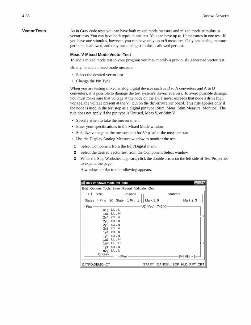
4-38 DIGITAL DEVICES
in est. If easure
test.
mage, high ly if The
erties
Vector Tests As in Gray code tests you can have both mixed mode measure and mixed mode stimulus vector tests. You can have both types in one test. You can have up to 10 measures in one tyou have one stimulus, however, you can have only up to 9 measures. Only one analog mper burst is allowed, and only one analog stimulus is allowed per test.
Meas V Mixed Mode Vector TestTo add a mixed mode test to your program you may modify a previously generated vector
Briefly, to add a mixed mode measure
• Select the desired vector test
• Change the Pin Type.
When you are testing mixed analog digital devices such as D to A converters and A to D converters, it is possible to damage the test system’s driver/receivers. To avoid possible dayou must make sure that voltage at the node on the DUT never exceeds that node’s drive voltage, the voltage present at the V+ pin on the driver/receiver board. This rule applies onthe node is used in the test step as a digital pin type (Stim, Meas, Stim/Measure, Monitor).rule does not apply if the pin type is Unused, Meas V, or Stim V.
• Specify when to take the measurement
• Enter your specifications in the Mixed Mode window
• Stabilize voltage on the measure pin for 50 µs after the measure state
• Use the Display Analog Measure window to monitor the test
1 Select Component from the Edit/Digital menu.
2 Select the desired vector test from the Component Select window.
3 When the Step Worksheet appears, click the double arrow on the left side of Test Propto expand the page.
A window similar to the following appears.
18xx Windows mode-init_com
Edit Options Tools Revert Validate QuitSave
START CANCEL SOF HLD RPT CRT
States 4 Pins 20 State
Size Position
1 Pin 1
Markers
Mark 1: 0 Mark 2: 3
C:\TPD\DEMO-ICT
Pins
Ignores
n1g1a12y42y32y22y21y41y31a31a41y1n2g
LLxxxxxxLLxL
LLxxxxxxLLxL
LLuuuuuuLLuL
LHuuuuuuHHuL
U2 (Vec) 74240
[Prev] [Next]
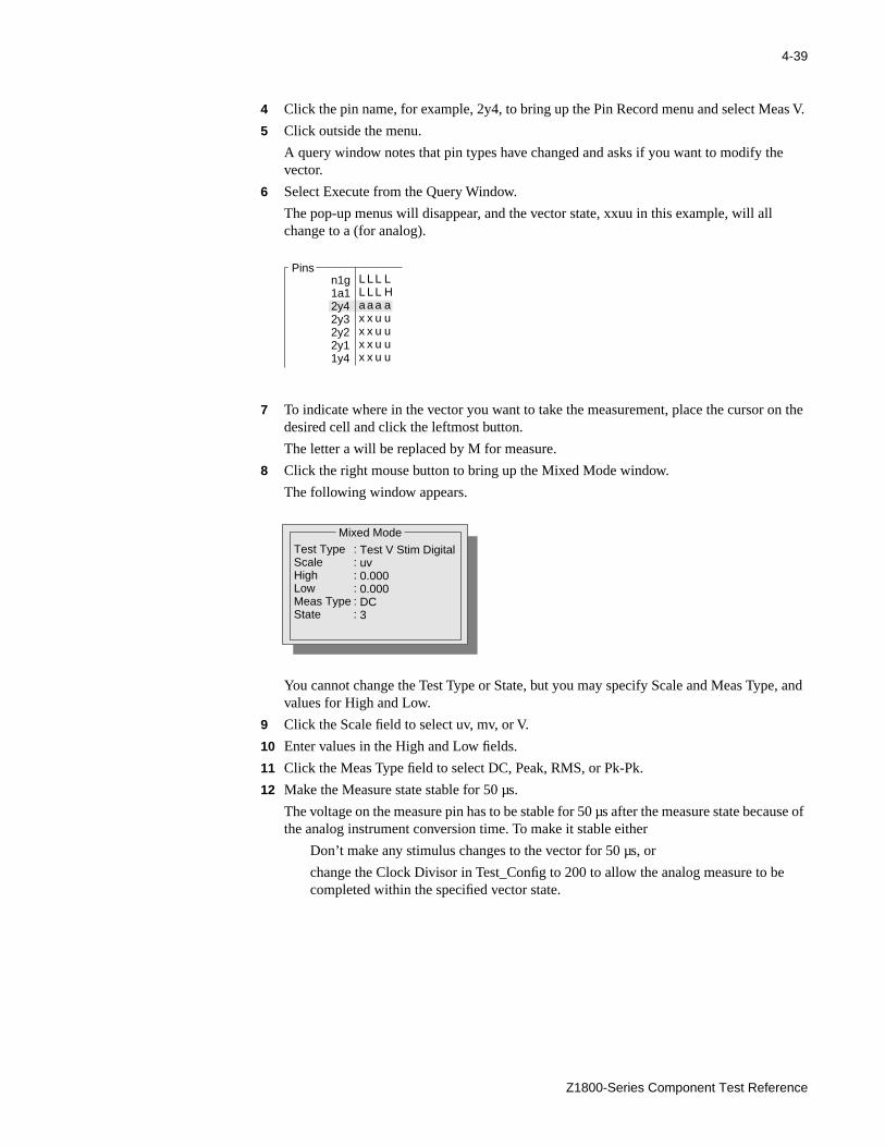
4-39
as V.
e
n the
e, and
ause of
e
4 Click the pin name, for example, 2y4, to bring up the Pin Record menu and select Me
5 Click outside the menu.
A query window notes that pin types have changed and asks if you want to modify thvector.
6 Select Execute from the Query Window.
The pop-up menus will disappear, and the vector state, xxuu in this example, will all change to a (for analog).
7 To indicate where in the vector you want to take the measurement, place the cursor odesired cell and click the leftmost button.
The letter a will be replaced by M for measure.
8 Click the right mouse button to bring up the Mixed Mode window.
The following window appears.
You cannot change the Test Type or State, but you may specify Scale and Meas Typvalues for High and Low.
9 Click the Scale field to select uv, mv, or V.
10 Enter values in the High and Low fields.
11 Click the Meas Type field to select DC, Peak, RMS, or Pk-Pk.
12 Make the Measure state stable for 50 µs.
The voltage on the measure pin has to be stable for 50 µs after the measure state becthe analog instrument conversion time. To make it stable either
Don’t make any stimulus changes to the vector for 50 µs, or
change the Clock Divisor in Test_Config to 200 to allow the analog measure to bcompleted within the specified vector state.
Pinsn1g1a12y42y32y22y11y4
LLaxxxx
LLaxxxx
LLauuuu
LHauuuu
Mixed ModeTest TypeScaleHighLowMeas TypeState
::::::
Test V Stim Digitaluv0.0000.000DC3
Z1800-Series Component Test Reference
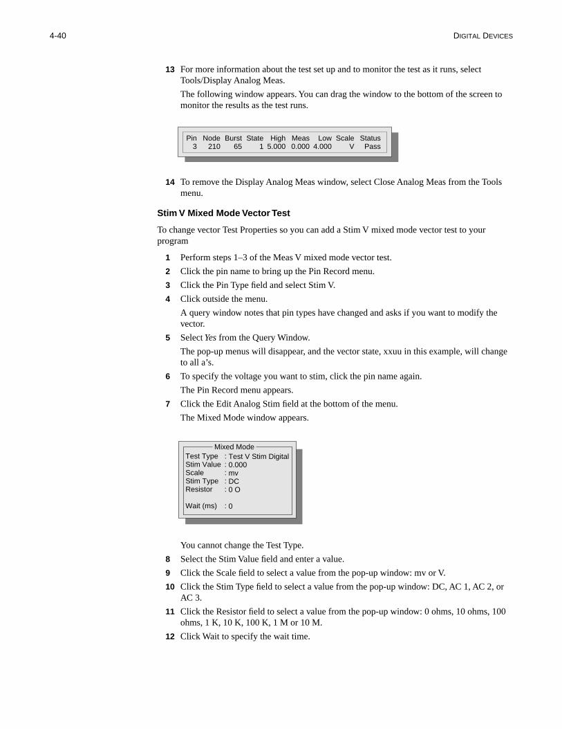
4-40 DIGITAL DEVICES
to
ls
e
nge
r
00
13 For more information about the test set up and to monitor the test as it runs, select Tools/Display Analog Meas.
The following window appears. You can drag the window to the bottom of the screenmonitor the results as the test runs.
14 To remove the Display Analog Meas window, select Close Analog Meas from the Toomenu.
Stim V Mixed Mode Vector Test
To change vector Test Properties so you can add a Stim V mixed mode vector test to yourprogram
1 Perform steps 1–3 of the Meas V mixed mode vector test.
2 Click the pin name to bring up the Pin Record menu.
3 Click the Pin Type field and select Stim V.
4 Click outside the menu.
A query window notes that pin types have changed and asks if you want to modify thvector.
5 Select Yes from the Query Window.
The pop-up menus will disappear, and the vector state, xxuu in this example, will chato all a’s.
6 To specify the voltage you want to stim, click the pin name again.
The Pin Record menu appears.
7 Click the Edit Analog Stim field at the bottom of the menu.
The Mixed Mode window appears.
You cannot change the Test Type.
8 Select the Stim Value field and enter a value.
9 Click the Scale field to select a value from the pop-up window: mv or V.
10 Click the Stim Type field to select a value from the pop-up window: DC, AC 1, AC 2, oAC 3.
11 Click the Resistor field to select a value from the pop-up window: 0 ohms, 10 ohms, 1ohms, 1 K, 10 K, 100 K, 1 M or 10 M.
12 Click Wait to specify the wait time.
Pin3
Node210
Burst65
State1
High5.000
Meas0.000
Low4.000
ScaleV
StatusPass
Mixed ModeTest TypeStim ValueScaleStim TypeResistor
Wait (ms)
:::::
:
Test V Stim Digital0.000mvDC0 O
0

4-41
stim.
ough
The wait time specifies the delay of the vector burst after the application of the analog
You may want to add time to the vector burst so that the digital state persists long enfor a proper analog sample to be taken.
Wait Time
Z1800-Series Component Test Reference
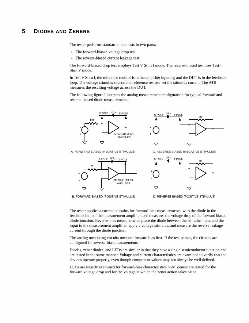
est I
back
d
biased d the kage
e
n and that the
5 DIODES AND ZENERS
The tester performs standard diode tests in two parts:
• The forward-biased voltage drop test
• The reverse-biased current leakage test
The forward-biased drop test employs Test V Stim I mode. The reverse-biased test uses TStim V mode.
In Test V Stim I, the reference resistor is in the amplifier input leg and the DUT is in the feedloop. The voltage stimulus source and reference resistor set the stimulus current. The ATBmeasures the resulting voltage across the DUT.
The following figure illustrates the analog measurement configuration for typical forward anreverse-biased diode measurements.
The tester applies a current stimulus for forward-bias measurements, with the diode in thefeedback loop of the measurement amplifier, and measures the voltage drop of the forwarddiode junction. Reverse-bias measurements place the diode between the stimulus input aninput to the measurement amplifier, apply a voltage stimulus, and measure the reverse leacurrent through the diode junction.
The analog measuring circuits measure forward bias first. If the test passes, the circuits arconfigured for reverse-bias measurements.
Diodes, zener diodes, and LEDs are similar in that they have a single semiconductor junctioare tested in the same manner. Voltage and current characteristics are examined to verify devices operate properly, even though component values may not always be well defined.
LEDs are usually examined for forward-bias characteristics only. Zeners are tested for the forward voltage drop and for the voltage at which the zener action takes place.
+
-
MEASUREMENTAMPLIFIER
RcCR X F POLEE POLE
+
-
MEASUREMENTAMPLIFIER
RcCR X F POLEE POLE
+
-
MEASUREMENTAMPLIFIER
CR X E POLEF POLE
+
-
MEASUREMENTAMPLIFIER
CR X E POLEF POLE
D. REVERSE BIASED (POSITIVE STIMULUS)
C. REVERSE BIASED (NEGATIVE STIMULUS)A. FORWARD BIASED (NEGATIVE STIMULUS)
B. FORWARD BIASED (POSITIVE STIMULUS)
Rc
Rc
+
-
+
-
+
-
+
-

5-2 DIODES AND ZENERS
t
ters
odes, Figure The
rance ge d test
of the the u can
The following figure illustrates typical diode and LED circuits. (Sample nodes are circled.)
Testing Diodes & Zeners
When developing a diode test, determine if the diode is silicon or germanium. The type determines the shorthand test values and longhand test parameters. The default diode tesassumes that the DUT is a silicon diode. More critical measurement of the forward and reverse-biased characteristics is possible by determining the actual measurement paramefrom the component's data sheet.
If a diode is in parallel with a resistor, it may not be possible to perform a reverse-biased measurement . The shorthand diode test works well with normal silicon and germanium dibut not with other single junction semiconductor devices such as LEDs and zeners diodes. B in the previous drawing is a simplified schematic representation of a typical LED circuit. DIALCO 521-9203 LED has the parameters:
• Forward Voltage: 2.0V typical, 1.8 min. 2.8 maximum
• Forward Current: 10 mA nominal
• Reverse Voltage: 3.0 Volts maximum
• Reverse Current: 1.0µA typical, 10µA maximum
Your test program would configure the analog test circuits for Test V Stim I and set the toleat ±20% of expected value. Although ±20% is a relatively wide tolerance, the forward voltadrop of the LED does not require a more critical one. The diode value for the forward-biaseis the typical forward voltage parameter.
Do not connect the E pole to a power bus. Instead, connect the E pole to the cathode sideLED and apply a negative stimulus to satisfy the polarity requirements for forward-biasing LED. It is not necessary to perform a reverse-biased measurement of the LED, although yodo so by applying a positive stimulus and changing to Test I Stim V configuration.
R961K 5%
121
U12U13
CR1
CR2R7
100K 5%
R97100K 5%
116
117 118
119
123
120
122
A
U7
R2330 5%
DS131
2
+5V
17
16
19 20 4
B
W
5-3
er is a se
ard test is ulus
harge
ams system g test
test es range.
heet
ues are s have
Zener Test Properties configures the analog measuring circuits in Test V Stim I mode. Zentwo-part test. The first part is a normal forward voltage drop test; the second part is a reverzener voltage test. For voltage protection, the program will abort if the first test fails. The maximum voltage you may apply to a board if the zener is missing is 2 Volts during the forwtest. Testing the forward voltage determines the presence of the device. If the zener voltageperformed with no device, the board is exposed to at least 13 Volts. The default current stimvalue for this test is 10 mA.
Zener Diodes in parallel with CapacitorsWhen you test zener diodes that are in parallel with capacitors, it is important to have a disctest page after the zener test to discharge any potential charge held by the capacitor.
Programs generated under F.0 automatically add a discharge page to zener tests. In progrgenerated before F.0, you should manually add the discharge test page to protect your testfrom the potential damage that could occur as a result of high guard currents from followinsteps.
Range and Accuracy The Range column states the testable range of diode and zener values. The accuracy of atechnique at a given range is opposite each row of ranges. (Device tolerance also influencaccuracy.) The Stimulus column displays the shorthand stimulus applied within the stated
*99.99 V with the High Voltage Option
The following factors influence shorthand test accuracy:
• Shorthand accuracy tolerance
• Guard ratio error tolerance
Step Worksheet Editing
You can edit a diode or zener test step at any time from the Step Worksheet. A Step Workscontains a menu bar, Component Properties, and Test Properties.
To access a diode or zener Step Worksheet from the Main menu, select
1 The board program
2 Edit
3 Semi
4 Diodes or Zeners
5 A diode ID (CR1, for example), or zener ID (VR1, for example) from the Component Select window.
Component Properties EditingRefer to the Z1800-Series Programmer’s Guidebook , Chapter 3, for specific details about editing the Component Properties.
Note that diodes do not have value or tolerance fields because the forward voltage test valpredetermined by the software and reported in Test Properties High and Low fields. Zenera single tolerance percentage field.
Test Range Accuracy Stimulus
Forward Voltage 0.00 to 9.99 V 0.02 % ± 1 mV 10 mA
Zener Voltage 0.00 to 9.99 V* 0.02 % ± 10 mV 10 mA
Reverse Leakage 0 to 999 µA 5 % 3.000 V DC
Z1800-Series Component Test Reference
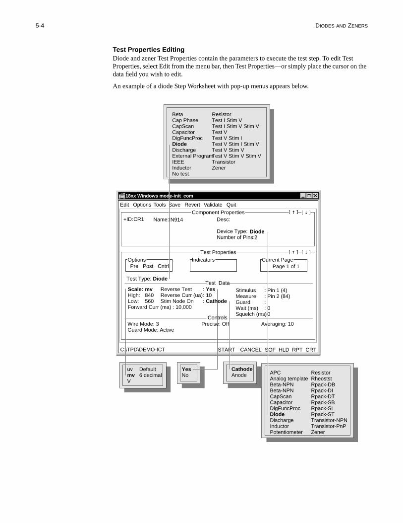
5-4 DIODES AND ZENERS
est on the
Test Properties EditingDiode and zener Test Properties contain the parameters to execute the test step. To edit TProperties, select Edit from the menu bar, then Test Properties—or simply place the cursordata field you wish to edit.
An example of a diode Step Worksheet with pop-up menus appears below.
CathodeAnode
YesNo
BetaCap PhaseCapScanCapacitorDigFuncProcDiodeDischargeExternal ProgramIEEEInductorNo test
ResistorTest I Stim VTest I Stim V Stim VTest VTest V Stim ITest V Stim I Stim VTest V Stim VTest V Stim V Stim VTransistorZener
18xx Windows mode-init_com
Page 1 of 1
Test Data
Controls
Edit Options Tools Revert Validate QuitSave
Component Properties
Test Properties Options Indicators
Pre Post CntrlCurrent Page
START CANCEL SOF HLD RPT CRT
Test Type: Diode
+ID: Name: Desc:
Device Type:Number of Pins:
CR1 IN914
Diode2
C:\TPD\DEMO-ICT
Scale:High:Low:Forward Curr (ma) : 10,000
mv840560
StimulusMeasureGuardWait (ms)Squelch (ms)
:::::
Pin 1 (4)Pin 2 (84)
00
Wire Mode: 3 Precise: Off Averaging: 10Guard Mode: Active
Reverse TestReverse Curr (ua)Stim Node On
Yes10Cathode
:::
uvmvV
APCAnalog templateBeta-NPNBeta-NPNCapScanCapacitorDigFuncProcDiodeDischargeInductorPotentiometer
ResistorRheoststRpack-DBRpack-DIRpack-DTRpack-SBRpack-SIRpack-STTransistor-NPNTransistor-PnPZener
Default6 decimal

5-5
Test Properties fields specific to diodes are described in the following table.
Upper Test Properties Area
Field Description
Test Type: The type of test configuration used in current Test Properties. Recommended for diodes:
Diode Shorthand diode test
IEEE IEEE instrument test
Test I Stim V Voltage stimulus and current measurement test (for reverse leakage)
Test V Stim I Current stimulus and voltage measurement test (for forward or breakdown—zener—voltage)
Test Data/Middle Test Properties Area
Scale Value field’s unit modifier based on Test Type
Diode uv, mv, V
Test I Stim V na, ua, ma
Test V Stim I uv, mv, V
High High limit of forward voltage drop test. Higher measurement sets fail flag.
Low Low limit of forward voltage drop test. Higher measurement sets fail flag
Reverse Test YES or NO. When YES, performs reverse leakage test.
Reverse Curr (ma) When Reverse Test is YES, enter number in range of 0 to 999 (ua).
Stim Node On Anode or Cathode, to control polarity of stimulus voltage and orientation of diode in test circuit.
Z1800-Series Component Test Reference
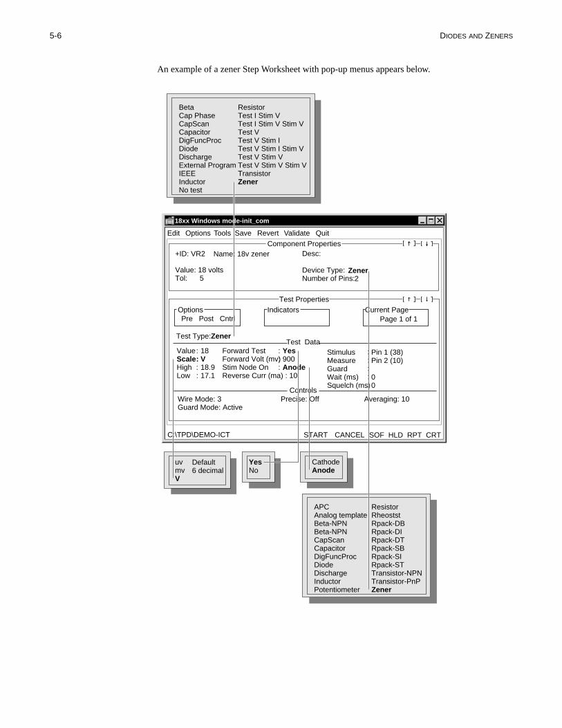
5-6 DIODES AND ZENERS
An example of a zener Step Worksheet with pop-up menus appears below.
BetaCap PhaseCapScanCapacitorDigFuncProcDiodeDischargeExternal ProgramIEEEInductorNo test
ResistorTest I Stim VTest I Stim V Stim VTest VTest V Stim ITest V Stim I Stim VTest V Stim VTest V Stim V Stim VTransistorZener
18xx Windows mode-init_com
Page 1 of 1
Test Data
Controls
Edit Options Tools Revert Validate QuitSave
Component Properties
Test Properties Options Indicators
Pre Post CntrlCurrent Page
START CANCEL SOF HLD RPT CRT
Test Type:Zener
Desc:
Device Type:Number of Pins:
Zener2
C:\TPD\DEMO-ICT
Wire Mode: 3 Precise: Off Averaging: 10Guard Mode: Active
APCAnalog templateBeta-NPNBeta-NPNCapScanCapacitorDigFuncProcDiodeDischargeInductorPotentiometer
ResistorRheoststRpack-DBRpack-DIRpack-DTRpack-SBRpack-SIRpack-STTransistor-NPNTransistor-PnPZener
+ID: VR2
Value: 18 voltsTol: 5
Name: 18v zener
ValueScaleHighLow
18V18.917.1
StimulusMeasureGuardWait (ms)Squelch (ms)
::::
:::::
Pin 1 (38)Pin 2 (10)
00
Forward TestForward Volt (mv)Stim Node OnReverse Curr (ma) : 10
Yes900Anode
:::
CathodeAnode
YesNo
uvmvV
Default6 decimal
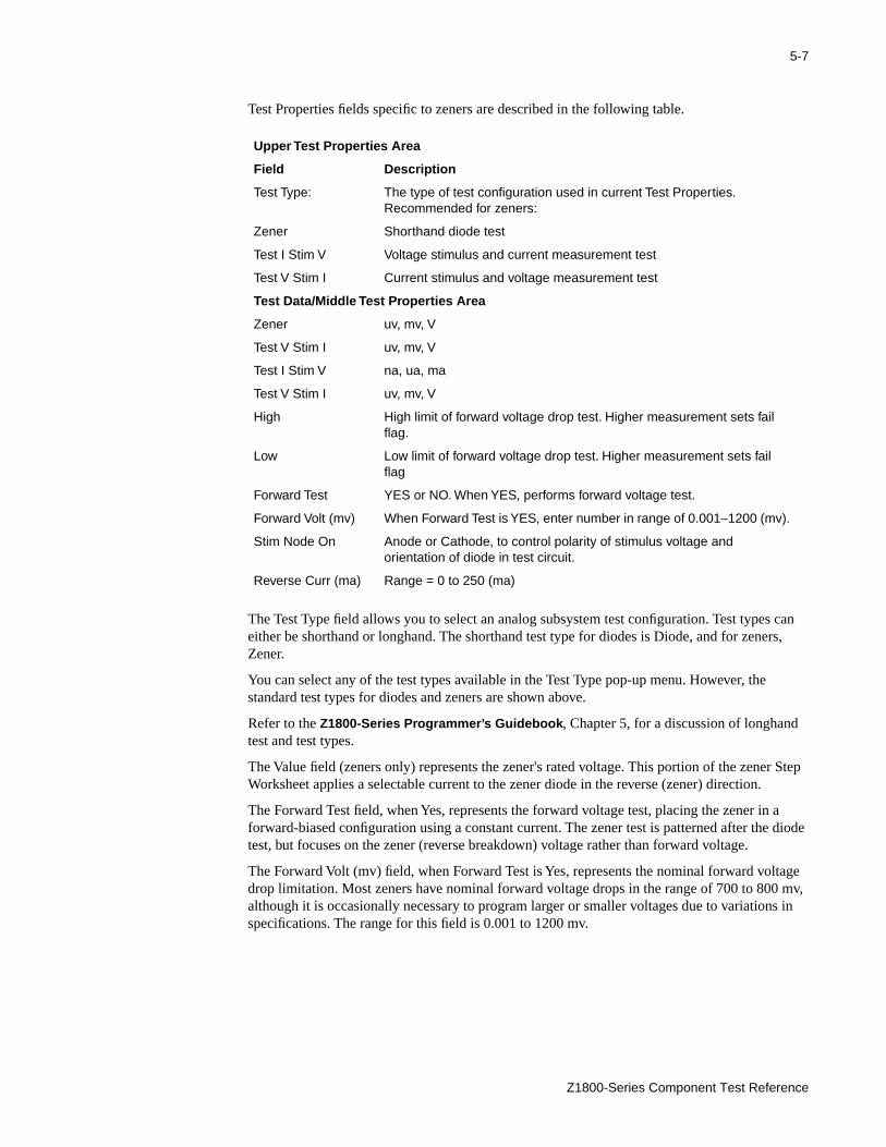
5-7
can rs,
r Step
a diode
age mv, s in
Test Properties fields specific to zeners are described in the following table.
The Test Type field allows you to select an analog subsystem test configuration. Test typeseither be shorthand or longhand. The shorthand test type for diodes is Diode, and for zeneZener.
You can select any of the test types available in the Test Type pop-up menu. However, thestandard test types for diodes and zeners are shown above.
Refer to the Z1800-Series Programmer’s Guidebook , Chapter 5, for a discussion of longhandtest and test types.
The Value field (zeners only) represents the zener's rated voltage. This portion of the zeneWorksheet applies a selectable current to the zener diode in the reverse (zener) direction.
The Forward Test field, when Yes, represents the forward voltage test, placing the zener inforward-biased configuration using a constant current. The zener test is patterned after thetest, but focuses on the zener (reverse breakdown) voltage rather than forward voltage.
The Forward Volt (mv) field, when Forward Test is Yes, represents the nominal forward voltdrop limitation. Most zeners have nominal forward voltage drops in the range of 700 to 800although it is occasionally necessary to program larger or smaller voltages due to variationspecifications. The range for this field is 0.001 to 1200 mv.
Upper Test Properties Area
Field Description
Test Type: The type of test configuration used in current Test Properties. Recommended for zeners:
Zener Shorthand diode test
Test I Stim V Voltage stimulus and current measurement test
Test V Stim I Current stimulus and voltage measurement test
Test Data/Middle Test Properties Area
Zener uv, mv, V
Test V Stim I uv, mv, V
Test I Stim V na, ua, ma
Test V Stim I uv, mv, V
High High limit of forward voltage drop test. Higher measurement sets fail flag.
Low Low limit of forward voltage drop test. Higher measurement sets fail flag
Forward Test YES or NO. When YES, performs forward voltage test.
Forward Volt (mv) When Forward Test is YES, enter number in range of 0.001–1200 (mv).
Stim Node On Anode or Cathode, to control polarity of stimulus voltage and orientation of diode in test circuit.
Reverse Curr (ma) Range = 0 to 250 (ma)
Z1800-Series Component Test Reference
5-8 DIODES AND ZENERS
ructs e of 3.0 . Enter a test
re the The
and tion
end of f time your
For diodes only, the Reverse Test field applies to standard diodes. When Yes, this field instthe tester to measure a diode's reverse current leakage characteristic by applying a voltagVDC (reverse bias) to the diode and then measuring the amount of current passing througha value in the range of 0–999 (na), which will be the maximum acceptable leakage currentthrough the diode in the Reverse Curr field. A measured value greater than that will result infailure. If you set Reverse Test to No, no reverse leakage test is performed.
IMPORTANTThe current should not exceed the maximum rated zener current.
For zener tests, the Reverse Curr (ma) field represents the stimulus current used to measuzener voltage. The current programmed is related to the wattage and voltage of the zener.default is 20 ma.
The Stim Node On field allows you to select the polarity of the zener with respect to the StimMeas terminals. Select either Anode or Cathode. With this field, you can control the orientaof the diode or zener in the test circuit and the configuration of the analog test subsystem.
The Squelch time on the Zener worksheet is applied both at the beginning of the page andthe page. At the end of the Zener page, the stimulus is turned off and waits for the amount oyou entered in the Wait and Squelch fields in order to discharge the nodes associated withZener test.
a test.
charge.
atteries may
es for rly orted
lso to
t rance
simply
6 DISCHARGE
The purpose of Discharge is to discharge capacitors on the board under test before runningDischarge test steps run at the beginning of a program, and are listed in the Intc section.
Discharge Testing Discharge Test Properties discharge only those nodes that have been programmed for disResidual charges can remain on nodes in the circuit that have not been programmed for discharge. This situation can happen if there are storage elements such as capacitors or bthat are isolated from the discharge node by an impedance. Although the passing voltagesreappear due to the memory effect of the large cap.
In addition, you can create an APC test step in the discharge section to test a range of nodcontact with the board under test early in the program. This Global APC feature is particulauseful if your boards are dirty or the fixture is unreliable to see if test execution should be aband the board under test recontacted.
Refer to page 3 for more information about adding an APC test step.
Discharging is essential to prevent damage to the board and to the tester relays. You can ainsert a discharge routine as Test Properties in a capacitor Step Worksheet when requireddischarge a capacitor.
To edit a discharge routine from the Main menu, select:
1 Edit
2 Intc
3 Discharge
4 A discharge ID from the Component Select window
Editing Refer to the Z1800-Series Programmer’s Guidebook , Chapter 3, for general information abouediting Component Properties. Discharge Step Worksheets, however, have no value or tolefields.
Test Properties EditingTo edit Discharge Test Properties, select Edit from the menu bar, then Test Properties—or place the cursor on the data field you wish to edit.

6-2 DISCHARGE
An example of a discharge Step Worksheet with pop-up menus appears below.
BetaCap PhaseCapScanCapacitorDigFuncProcDiodeDischargeExternal ProgramIEEEInductorNo test
ResistorTest I Stim VTest I Stim V Stim VTest VTest V Stim ITest V Stim I Stim VTest V Stim VTest V Stim V Stim VTransistorZener
18xx Windows mode-init_com
Page 1 of 1
Test Data
Controls
Edit Options Tools Revert Validate QuitSave
Component Properties
Test Properties Options Indicators
Pre Post CntrlCurrent Page
START CANCEL SOF HLD RPT CRT
Test Type:Discharge
Desc:
Device Type:Number of Pins:
Discharge2
C:\TPD\DEMO-ICT
Wire Mode: 3 Precise: Off Averaging: 10Guard Mode: Active
APCAnalog templateBeta-NPNBeta-NPNCapScanCapacitorDigFuncProcDiodeDischargeInductorPotentiometer
ResistorRheoststRpack-DBRpack-DIRpack-DTRpack-SBRpack-SIRpack-STTransistor-NPNTransistor-PnPZener
+ID: C8
Value: 18 voltsTol: 5
Name: 18v zener
uvmvV
5mv
MeasureGuard
::
::Pin 1 (46)Pin 2 (32)
Timeout (ms): 25000ThresholdScale
Default6 decimal

6-3
ors
se to
efault ged,
time, ieved
ems lems
cuted hile
again tion is
is iling iling
ast
small
Discharge steps are not automatically added when capacitors are added by hand. Capacitabove 50 uF must have an associated Discharge step.
The Test Type field allows you to select an analog test configuration or type the tester will uexecute the step. The test type for discharge steps is Discharge.
The Threshold and Scale fields define the voltage the capacitor will be discharged to. The dis set to 5 mV. Thresholds should not be set too high, otherwise tester relays can be damadepending on the size of the capacitor and its residual charge.
The Timeout field represents the maximum time allowed for the discharge test to reach its acceptable discharge voltage level. If the capacitor is not discharged within this amount of the discharge test will fail. Enter a value in the range of 0 to 32,000 ms. If discharge is achbefore the time expires, the test will automatically terminate.
Adding Discharge Test Step for Global APC
Dirty boards with an excess of flux residue or an unreliable fixture can cause contact problbetween the tester and the DUT. In such cases it is advisable to test for board contact probearly in the test program. The Global APC function provides this test capability.
Global APC should be done in the Discharge section after all the discharge steps have execorrectly. Using Global APC to test for board contact will weld reed relays when executed wthere are charged up capacitors present on the board. It may be prudent to run Discharge after the APC test because the APC test itself could charge up some capacitors. (This situaunlikely, however, since the stimulus time is short.)
To test for uncontacted nodes, Global APC uses a three-pass approach. First, every node measured for the specified current threshold while stimulating a -3 V stimulus. Then the fanodes (those below the threshold) will be tested in the same way with +3 V stimulus. Still fanodes are then tested with an AC stimulus and remaining failing nodes are reported. The lphase is optional and can be controlled by the Slow/Fast flag in Test Properties since it is considerably slower than the DC test. The AC test is meant to find nodes contacted only bycapacitors which cannot otherwise be found.
Should the APC test fail, the General Fail flag and the APC Fail flag will be set.
The generator token for APC is APC, and it follows the same syntax as Shorts—SH.
Upper Test Properties Area
Field Description
Test Type: The type of test configuration used in current Test Properties.
Discharge Shorthand discharge test.
Test Data/Middle Test Properties Area
Threshold Maximum residual voltage of Scale for proper discharging. Range = 0–999.
Scale Threshold field’s unit modifier. Choices are mv, V
Timeout Maximum time allowed to reach discharge voltage level. Range = 0–32000.
Z1800-Series Component Test Reference

6-4 DISCHARGE
in the
he
To create the Global APC Step Worksheet
1 Add a Step Worksheet at the end of the Discharge section.
2 When Component Properties appears, type an appropriate identification such as apcID field.
3 Click Device Type and select APC from the pop-up menu.
Be aware that range for the APC Threshold is 300 MOhms to 12KOhms.
1 Select Tools/Generate Test.
2 When the Test Properties page appears, fill in the node range you want to test APC on. Tsyntax is the same as it is in a shorts test.
18xx Windows mode-init_com
Page 1 of 1
Test Data
Controls
Edit Options Tools Revert Validate QuitSave
Component Properties
Test Properties Options Indicators
Pre Post CntrlCurrent Page
START CANCEL SOF HLD RPT CRT
Test Type:Discharge
Desc:
Device Type:Number of Pins:
Discharge2
C:\TPD\DEMO-ICT
Wire Mode: 3 Precise: Off Averaging: 10Guard Mode: Active
+ID: apc
Value:Tol:
Name:
5mv
MeasureGuard
::
::Pin 1 (46)Pin 2 (32)
Timeout (ms): 25000ThresholdScale
APCAnalog templateBeta-NPNBeta-NPNCapScanCapacitorDigFuncProcDiodeDischargeInductorPotentiometer
ResistorRheoststRpack-DBRpack-DIRpack-DTRpack-SBRpack-SIRpack-STTransistor-NPNTransistor-PnPZener
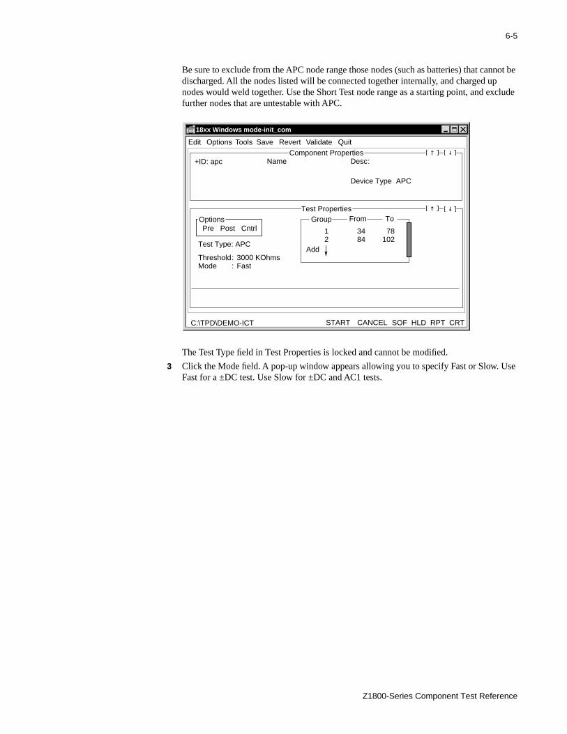
6-5
nnot be xclude
Use
Be sure to exclude from the APC node range those nodes (such as batteries) that cadischarged. All the nodes listed will be connected together internally, and charged upnodes would weld together. Use the Short Test node range as a starting point, and efurther nodes that are untestable with APC.
The Test Type field in Test Properties is locked and cannot be modified.
3 Click the Mode field. A pop-up window appears allowing you to specify Fast or Slow. Fast for a ±DC test. Use Slow for ±DC and AC1 tests.
18xx Windows mode-init_com
Test Type: Capacitor
Edit Options Tools Revert Validate QuitSave
Component Properties
Test Properties Options
Pre Post Cntrl
+ID: apc Name: Desc:
Device Type APC:
START CANCEL SOF HLD RPT CRTC:\TPD\DEMO-ICT
Test Type: APC
ThresholdMode
3000 KOhmsFast
::
Group From To
12
3484
78102
Add
Z1800-Series Component Test Reference

ested tance
and
et
7 INDUCTORS
The standard inductor is tested in Test I Stim V mode.
Inductors that are too small or too large to be measured accurately for inductance can be tfor presence on the board by measuring DC resistance. Most inductors have low DC resisand need to be declared as Ignore groups in the Intc test section.
The PRISM-Z (PRecision Integrated Signal Measurement) module is available as an optioncan be used for Inductor tests. Refer to the Z1800-Series PRISM-Z User’s Guide for a complete discussion about the PRISM-Z test types available for Inductor tests.
Range and Accuracy
Use the following listing as a guide for range and accuracy
*AC1 = 159.1 Hz; AC2 = 1.591 kHz; AC3 = 15.91 kHzSystem inductance: 5 µH typicalResistive component of inductor: measured and subtracted.
Shorthand test accuracy is affected by the following factors:
• Shorthand system accuracy
• System resistance, capacitance, or inductance (if not subtracted)
• Guard ratio error tolerance
• Device-under-test (DUT) tolerance
Step Worksheet Editing
You can edit an inductor test step at any time from the Step Worksheet. The Step Workshecontains a menu bar, Component Properties, and Test Properties.
To access an inductor Step Worksheet from the Main menu, select
1 The board program
2 Edit
3 Passive
4 Inductors
5 An inductor ID, such as L1 or L2, for example, from the Component Select window
Range Accuracy
3-Wire 6-Wire Stimulus*
10 to 29.99 µH 10 % ±10 µH 0.3V pk to pk AC3
30.0 to 299.9 µH 10 % ±10 µH 0.3V pk to pk AC3
300 to 2999 µH 5 % ±10 µH 0.3V pk to pk AC3
3.00 to 29.99 mH 8 % ±10 µH 5 % ±10 µH 0.3V pk to pk AC2
30.0 to 2999 mH 8 % NA 0.3V pk to pk AC2
3.00 to 29.99 H 8 % NA 0.3V pk to pk AC1
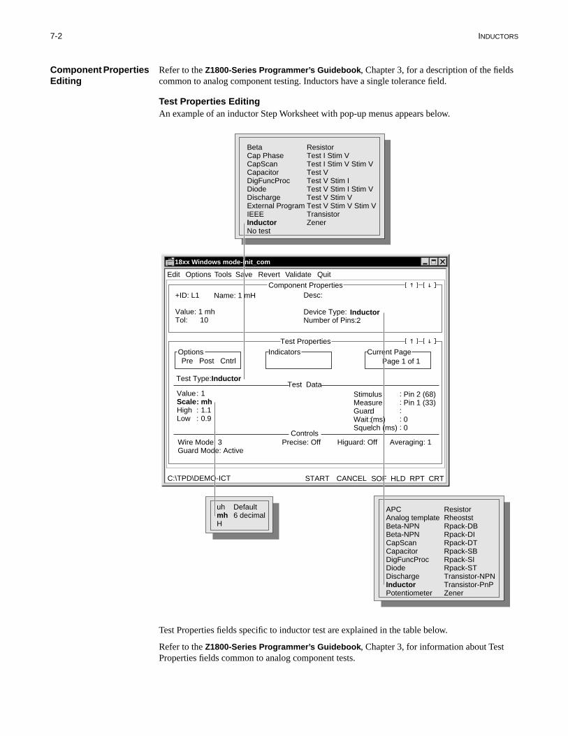
7-2 INDUCTORS
Component Properties EditingRefer to the Z1800-Series Programmer’s Guidebook , Chapter 3, for a description of the fieldscommon to analog component testing. Inductors have a single tolerance field.
Test Properties EditingAn example of an inductor Step Worksheet with pop-up menus appears below.
Test Properties fields specific to inductor test are explained in the table below.
Refer to the Z1800-Series Programmer’s Guidebook , Chapter 3, for information about Test Properties fields common to analog component tests.
BetaCap PhaseCapScanCapacitorDigFuncProcDiodeDischargeExternal ProgramIEEEInductorNo test
ResistorTest I Stim VTest I Stim V Stim VTest VTest V Stim ITest V Stim I Stim VTest V Stim VTest V Stim V Stim VTransistorZener
18xx Windows mode-init_com
Page 1 of 1
Test Data
Controls
Edit Options Tools Revert Validate QuitSave
Component Properties
Test Properties Options Indicators
Pre Post CntrlCurrent Page
START CANCEL SOF HLD RPT CRT
Test Type:Inductor
Desc:
Device Type:Number of Pins:
Inductor2
C:\TPD\DEMO-ICT
Wire Mode: 3 Precise: Off Higuard: Off Averaging: 1Guard Mode: Active
APCAnalog templateBeta-NPNBeta-NPNCapScanCapacitorDigFuncProcDiodeDischargeInductorPotentiometer
ResistorRheoststRpack-DBRpack-DIRpack-DTRpack-SBRpack-SIRpack-STTransistor-NPNTransistor-PnPZener
+ID: L1
Value: 1 mhTol: 10
Name: 1 mH
ValueScaleHighLow
1mh1.10.9
::::
:::::
uhmhH
StimulusMeasureGuardWait (ms)Squelch (ms)
:::::
Pin 2 (68)Pin 1 (33)
00
Default6 decimal

7-3
se to for
The Test Type field allows you to select an analog test configuration or type the tester will uexecute the step. Test types can be either shorthand or longhand. The shorthand test typeinductors is Inductor.
Upper Test Properties Area
Field Description
Test Type: The type of test configuration used in current Test Properties. Recommended for inductors:
Inductor Shorthand inductor test
Resistor Shorthand resistor test for inductors too small or too large for inductance
Test I Stim V Voltage stimulus and current measurement test
Test V Stim I Current stimulus and voltage measurement test
Test Data/Middle Test Properties Area
Value Numeric field specifying nominal expected value of Scale. Range = 0–1000.
Scale: Value field’s unit modifier based on Test Type
Inductor uh, mh, H
Resistor Ohms, Kohms, Mohms
Test I Stim V na, ua, ma
Test V Stim I uv, mv, V
Wait (ms) 0 to 32000 ms. Added to default wait of 3 ms typical.
Squelch (ms) 0 to 32000 ms. Repeatable initial condition to remove stored energy.
Z1800-Series Component Test Reference

rge l board
of om
ce, or
6, 78, signed
ance shold,
ty fails.
are
an be
d. Test
8 INTERCONNECTS
The Intc menu includes Discharge, Jumpers, Continuities, Ignores, Merge_Sc, Shorts, andOpens.
The interconnections test categories above are listed in the order of test execution. Dischatests are not interconnections but are executed in the Intc section to ensure that all residuacharges are dissipated at the beginning of a program.
See the Discharge Test Steps section for details about global discharging.
Continuities Tests and Editing
Continuities tests verify proper connectivity between node groups. Continuities are groupsnode number sets that are electrically connected in the same network. Continuities differ frjumpers. Jumpers are usually an assembled component that may be reported missing. Continuities are not physical components, but such things as multiple nodes on a board trathe presence of a trace, end to end.
For example, a continuity between nodes 12 and 34 comprises a continuity group. Nodes 5and 90, if electrically connected, would comprise a second group. Each group would be asa group number, starting with 1. The group number is reported in the event of a failure.
Each expected continuity should be entered in Test Properties. The tester measures resistbetween the indicated nodes. If the measurement is equal to or less than the continuity threthe nodes pass the continuity test. If the measurement exceeds the threshold, the continui
Continuities are also tested in the Ignores section to prevent shorting of other nodes, whichignored in the shorts test.
The measurement threshold is adjustable from 1 to 50 ohms. In other words, a continuity cdefined as having a resistance as high as 50 ohms. The default value for a continuity's measurement threshold is 5 ohms.
To edit a continuity Step Worksheet from the Main menu, select:
1 Edit
2 Intc
3 Continuities
4 A continuities ID from the Component Select window
Component Properties Editing
Component Properties contains fields of descriptive data about the component being testeProperties, however, determines how the test executes.
Refer to the Z1800-Series Programmer’s Guidebook , Chapter 3, for a description of all fields other than Value and Number of Conts.
An example of a Continuities Component Properties appears below.
The Device Type field is read-only for continuities tests.

8-2 INTERCONNECTS
on the
iately e
Test Properties Editing
Continuities Test Properties contain the parameters to execute the test step. To edit Test Properties, select Edit from the menu bar, then Test Properties—or simply place the cursordata field you wish to edit.
An example of a continuities Step Worksheet appears below.
To edit a group of nodes:
1 Select a group field.
A node editor window appears
2 To edit a node, place the cursor on the node you want to edit and type the new nodenumber.
The Enter key advances the cursor to the next field.
3 To add nodes, select the Add field by a single mouse click or by pressing Enter.
Type a node number in the empty field.
4 Select Save to save changes.
Select Revert to remove edits since last saved setup.
Test Properties fieldsThe following is a description of the Continuities Test Properties fields:
The Test Type field is always Continuity for continuities tests.
The Threshold field represents the measurement threshold value in ohms.
The Group field begins with 1. The Nodes fields associated with a group are shown immedto the right of the group number. Only the nodes listed are associated with each group. Usnumbers only to identify nodes.
Field Description
Options Pre-Test, Post-Test, and Controls. Read-only.
Test Type: Continuity
The type of test configuration used in current Test Properties.Continuities test. Read-only field.
Threshold Threshold value in Ohms. Range = 1 – 50. Default = 5.
Group Number of a node group.
Nodes Nodal address(es) of node(s) in a group.
35, 51, Add
Enter the Interconnect Node Number, F9 = Nodefinder
Add an Interconnect Node.
Type new node number to add a node to group
35, 51, Add
Enter the Interconnect Node Number, F9 = Nodefinder

8-3
false ors, ts
oint on n any
as a
outside orted.
or
missing ignal ard
ach ction
be rement
er that
for
Ignores Testing Ignores testing is a method of registering low impedance or unpredictable paths to preventreporting as a short during Shorts testing. Very low resistance inductors, very large capacitpotentiometers, and switches should also be entered into the Ignores table to prevent shorfailures.
Ignores verifies that no shorts exist between any nodes in an Ignores group and any other pthe printed circuit board not in the group. An Ignores group passes if the resistance betweenode in the group and all other nodes exceeds the ignore threshold. The Threshold field represents the measurement threshold value in Ohms. An Ignores group fails and reports short if any Ignores group node has less resistance to a node outside the group.
The threshold is adjustable from 2 to 50 ohms. The default value is 5 ohms.
The Threshold field is the threshold for the comparison to outside nodes. Any outside nodehaving less resistance than Threshold will fail as a short.
Nodes listed in an ignores group are not tested against each other but rather against nodesthe group, including other Ignores groups. If a short exists on an external node it will be rep
To edit an Ignores Step Worksheet from the Main menu, select:
1 Edit
2 Intc
3 Ignores
4 An ignores ID from the Component Select window
Ignores and continuities have the same editing features. Refer to the Continuities section fdetails about editing the Step Worksheet.
Jumpers Testing Jumpers are physical wires on the board under test that can be diagnosed erroneously as components if not accounted for in the Jumpers section. Jumpers may be connections of straces on the board under test, such as jumper blocks, zero-ohm resistors, and cuttable botraces. The difference between a jumper and a continuity is that a jumper is an identifiablecomponent with a name.
A jumper is tested as a set of electrically connected nodes, isolated from all other nodes. Ejumper group is given a group number as is the case with continuities and other interconnetests (except Discharge).
The measurement threshold is adjustable from 1 to 50 ohms. In other words, a jumper candefined as having a resistance as high as 50 ohms. The default value for a jumper's measuthreshold is 5 ohms. If the jumper you are testing has a value below 5 ohms, you must entvalue.
The Threshold field represents the measurement threshold value in Ohms.
To edit a jumper Step Worksheet from the Main menu, select
1 Edit
2 Intc
3 Jumpers
4 A jumper ID from the Component Select window
Jumpers and continuities have the same editing features. Refer to the Continuities sectiondetails about editing the Step Worksheet.
Z1800-Series Component Test Reference

8-4 INTERCONNECTS
horts ecified s
are in g
ise the
ted
s. The
e in the
this is ort is ported.
_SC
r
f the
orting
Merge_SC (Merge Special Case) Testing
The Merge_SC step provides two functions.
First, it is a summary table of all nodes that will not be reported as shorts in the standard Stest. This table is composed of all continuity groups, jumpered nodes, and those nodes spas ignores. Programmers should examine this table to verify that all nodes and node grouplisted, in fact, should not be tested in the regular Shorts test.
Second, Merge_SC tests nodes itself. All continuity groups, jumpered, and ignored nodes tested for shorts against all other nodes outside their own group. This includes both nodesother MERGE_SC groups as well as all others that fall into the ranges listed in the followinSHORTS Step Worksheet test steps.
During program debug, the Merge_SC section must be run prior to the Shorts step, otherwshorts testing algorithm will see all of the Merge_SC nodes as shorts.
Shorts Tests and Editing
A shorts group is a set of node numbers tested to verify that each node is electrically isolafrom all the others in the group. (The Merge_Sc—merge special cases—Step Worksheet summarizes all exceptions to the shorts node range.) You can define multiple shorts groupnodes in each group will be checked against all other node groups.
Usually the ranges of nodes cover the lowest numbered node to the highest numbered nodfixture.
The Threshold field represents the measurement threshold value in ohms.
The Wait field allows you to enter a wait time (in ms) for short measurements. You can usefeature to prevent large capacitors from being reported as shorts. The wait time you enter applied when a measurement indicates a short. A secondary measure is taken, and if a shstill indicated, the short is reported; if the delayed measure passes, then the short is not re
The wait time you enter on the Shorts Test Properties applies to the Short test and Mergedtesting.
Shorts Specifications:
Range: 0.0 to 100.00 OhmsResolution: 0.1 ΩAccuracy: 5% ±0.5 ΩStimulus: 0.2 V dcDefault: 5 Ohms
To edit a shorts Step Worksheet from the Main menu, select
1 Edit
2 Intc
3 Shorts
4 A shorts ID from the Component Select window
Shorts and continuities have the same editing features. Refer to the Continuities section fodetails about editing the Step Worksheet.
Opens Testing Opens tests are used only for the fixture selftest and should not be part of an in-circuit testprogram. Used for fixture verification, this test measures probe resistance. As the inverse oshorts test, it reports all the nodes not in contact with the shorting plate. You will need a shplate for an opens test.
8-5
g
To edit an opens Step Worksheet from the Main menu, select
1 Edit
2 Intc
3 Opens
4 An opens ID from the Component Select window
A window similar to the following appears
The opens range should include the range of nodes that pertain to the specific fixture.
Nodes showing a higher resistance value than the program threshold are reported as failinnodes. You must replace such nodes before testing can begin.
18xx Windows mode-init_com
Test Type: Capacitor
Edit Options Tools Revert Validate QuitSave
Component Properties
Test Properties Options
Pre Post Cntrl
+ID: apc Name: Desc:
Device Type Opens:
START CANCEL SOF HLD RPT CRTC:\TPD\DEMO-ICT
Test Type: Opens
Threshold 5 Ohms:
Group From To
Add
Z1800-Series Component Test Reference

r clude log
ntains
d.
9 LINEAR ANALOG
Linear tests can be tests of special analog devices requiring power, or they can be tests fomeasuring voltage at some point at a nodal address. Devices in the Linear category can inoperation amplifiers, voltage regulators, comparators, and even relays. (To test special anadevices with power off, use the PwrOff category.)
Shorthand test accuracy is affected by the following factors:
• Shorthand system accuracy
• System resistance, capacitance, or inductance (if not subtracted)
• Guard ratio error tolerance
• Device-under-test (DUT) tolerance
Longhand test accuracy is affected by the following factors:
• Stimulus tolerance
• Measurement tolerance
• Guard ratio error tolerance
• Device-under-test (DUT) tolerance.
You can edit a linear test step at any time from the Step Worksheet. The Step Worksheet coa menu bar, Component Properties, and Test Properties, all of which appear below.
To open an analog linear Step Worksheet from the Main menu, select
1 Edit
2 Linear
3 A linear ID from the Component Select window
Editing Component Properties contains fields of descriptive data about the component being teste
Refer to the Z1800-Series Programmer’s Guidebook , Chapter 3, for a description of the fieldscommon to component testing.
Linear tests, however, have a single Device Type field, Analog Template.
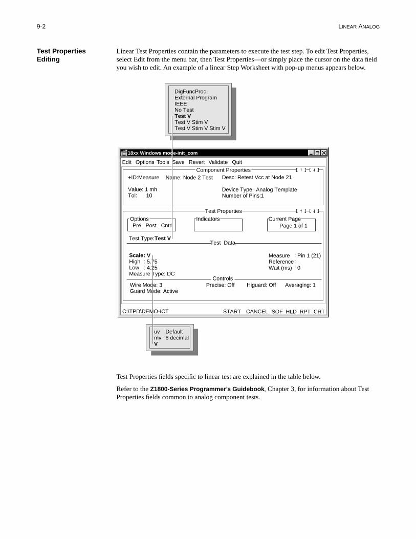
9-2 LINEAR ANALOG
ties, a field .
Test Properties Editing
Linear Test Properties contain the parameters to execute the test step. To edit Test Properselect Edit from the menu bar, then Test Properties—or simply place the cursor on the datyou wish to edit. An example of a linear Step Worksheet with pop-up menus appears below
Test Properties fields specific to linear test are explained in the table below.
Refer to the Z1800-Series Programmer’s Guidebook , Chapter 3, for information about Test Properties fields common to analog component tests.
18xx Windows mode-init_com
Page 1 of 1
Test Data
Controls
Edit Options Tools Revert Validate QuitSave
Component Properties
Test Properties Options Indicators
Pre Post CntrlCurrent Page
START CANCEL SOF HLD RPT CRT
Test Type:Test V
Desc: Retest Vcc at Node 21
Device Type:Number of Pins:
Analog Template1
C:\TPD\DEMO-ICT
Wire Mode: 3 Precise: Off Higuard: Off Averaging: 1Guard Mode: Active
+ID:Measure
Value: 1 mhTol: 10
Name: Node 2 Test
ScaleHighLowMeasure Type: DC
V5.754.25
:::
uvmvV
Default6 decimal
MeasureReferenceWait (ms)
:::
Pin 1 (21)
0
DigFuncProcExternal ProgramIEEENo TestTest VTest V Stim VTest V Stim V Stim V
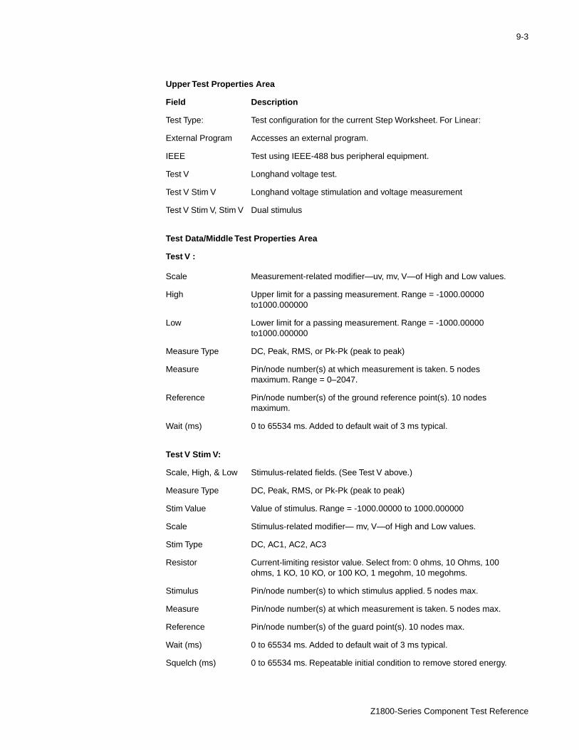
9-3
Upper Test Properties Area
Field Description
Test Type: Test configuration for the current Step Worksheet. For Linear:
External Program Accesses an external program.
IEEE Test using IEEE-488 bus peripheral equipment.
Test V Longhand voltage test.
Test V Stim V Longhand voltage stimulation and voltage measurement
Test V Stim V, Stim V Dual stimulus
Test Data/Middle Test Properties Area
Test V :
Scale Measurement-related modifier—uv, mv, V—of High and Low values.
High Upper limit for a passing measurement. Range = -1000.00000 to1000.000000
Low Lower limit for a passing measurement. Range = -1000.00000 to1000.000000
Measure Type DC, Peak, RMS, or Pk-Pk (peak to peak)
Measure Pin/node number(s) at which measurement is taken. 5 nodes maximum. Range = 0–2047.
Reference Pin/node number(s) of the ground reference point(s). 10 nodes maximum.
Wait (ms) 0 to 65534 ms. Added to default wait of 3 ms typical.
Test V Stim V:
Scale, High, & Low Stimulus-related fields. (See Test V above.)
Measure Type DC, Peak, RMS, or Pk-Pk (peak to peak)
Stim Value Value of stimulus. Range = -1000.00000 to 1000.000000
Scale Stimulus-related modifier— mv, V—of High and Low values.
Stim Type DC, AC1, AC2, AC3
Resistor Current-limiting resistor value. Select from: 0 ohms, 10 Ohms, 100 ohms, 1 KO, 10 KO, or 100 KO, 1 megohm, 10 megohms.
Stimulus Pin/node number(s) to which stimulus applied. 5 nodes max.
Measure Pin/node number(s) at which measurement is taken. 5 nodes max.
Reference Pin/node number(s) of the guard point(s). 10 nodes max.
Wait (ms) 0 to 65534 ms. Added to default wait of 3 ms typical.
Squelch (ms) 0 to 65534 ms. Repeatable initial condition to remove stored energy.
Z1800-Series Component Test Reference

9-4 LINEAR ANALOG
t step.
est
The Linear Test Type allows you to select a test configuration or test type to execute the tesLinear test types are either longhand or IEEE.
You can select any of the test types available in the Test Type pop-up at left. If the device tdoes not already exist, Test Properties initially comes up as Test Type, No Test.
Test V Stim V Stim V:
Scale, High, & Low Measurement-related fields. (See Test V above.)
Measure Type DC, Peak, RMS, or Pk-Pk (peak to peak)
Stim 1 Value Value of stimulus. Range = -1000.0 to +1000.0
Stim 1 Scale mv or V
Stim 1 Type DC, AC1, AC2, AC3
Resistor 1 Current-limiting resistor value. Select from: 0 ohms, 10 ohms, 100 ohms, 1 KO, 10 KO, or 100 KO, 1 megohms, 10 megohms
Stim 2 Value (V) -6.4 to +6.4 V
Resistor 2 10 ohms, 100 ohms, 1 KO
Stimulus 1 Same as Test V Stim V. Note: Stim 1 and Stim 2 nodes can’t be in same group of 16 nodes.
Stimulus 2 Same as Test V Stim V. Note: Stim 1 and Stim 2 nodes can’t be in same group of 16 nodes.
Measure Pin/node number(s) at which measurement is taken. 5 nodes max.
Reference Pin/node number(s) of the guard point(s). 10 nodes max.
Wait (ms) 0 to 65534 ms. Added to default wait of 3 ms typical.
Squelch (ms) 0 to 65534 ms. Repeatable initial condition to remove stored energy.
External Program:
Scale pico, nano, micro, milli, unit, Kilo, Mega
High, Low Upper and lower limits of passing measurements.
Mem Req Swap space needed for external program to run.
E pole Pin/node number(s) to which stimulus applied. 5 nodes max.
F pole Pin/node number(s) at which measurement is taken. 5 nodes max.
G pole Pin/node number(s) of the guard point(s). 10 nodes max.
IEEE See the IEEE section of the Z1800-Series Options Manual for details.

to test, all
off
10 POWER-OFF LONGHAND ANALOG
The PwrOff test category accommodates special analog devices that do not require power such as thermistors, MOV devices, varistors, thyristors devices requiring explicit control of voltages and current, and tests employing IEEE instrumentation. The PwrOff category alsoprovides access to the MultiScan tests: FrameScan, WaveScan, and DeltaScan.
See the Multiscan User’s Guide for additional information about the PwrOff category.
To access either Analog or MultiScan test sections from the Main menu, select:
1 The board program
2 Edit
3 PwrOff
4 Analog, DeltaScan, or Frame/WaveScan/FS+
Use the Linear category to perform power-on analog longhand testing.
Refer to Chapter 1, Shorthand and Longhand Theory, for detailed information about powerlonghand analog tests.
Files Edit Run Pgen Setup Utility Templates ConvertEdit
Header Intc Passive Semi Analog Brd_Power Linear Digital Trailer QuitPwrOff
AnalogDeltaScanFrame/WaveScan/FS+

tion to a section ion
r with stic tated ing for other
r wiper
ts the
fully ion. passes can
While y to
to rate of
11 POTENTIOMETERS AND RHEOSTATS
Potentiometers and rheostats are variable resistance devices that require operator interacensure that they are tested properly. Potentiometers, rheostats, and switches are tested as before the other passive analog devices to avoid guarding problems. The following illustratshows typical potentiometer (R3) and rheostat (R1) circuits. (Sample nodes are circled.)
Both potentiometers and rheostats are tested with essentially the same two techniques.
A potentiometer is usually examined in two pages of a single test step as a variable resistotwo independent resistances. For potentiometers, your program must ensure that a diagnomessage is not generated even if the measurement is outside the bounds defined by the stolerance. The first half of the test instructs the operator to center the potentiometer by testhalf of the potentiometer's value. After the potentiometer is adjusted, the tester checks thehalf.
A rheostat test step measures the overall resistance value, then sets the variable output, oarm, of the resistor to a predetermined value.
The two-terminal rheostat method ensures that the wiper arm is working properly and preseoutput of the device, reducing calibration time during later assembly operations.
The rheostat program should instruct the operator to set the wiper arm of the rheostat to acounterclockwise position, then press the tabletop Start button to continue program executThe program should check to ensure that the value of the rheostat is correct. If the rheostatthe first part of this examination, instruct the test to repeat on a failure loop so the operatoradjust for some value, otherwise generate a failure message and skip the loop.
You can use Repeat to repeat the associated test until the operator presses the Start key. Repeat is active (On), the display line is also enabled so that the operator can observe themeasurement data. When the adjustment is complete, have the operator press the Start kecontinue testing. Perform the measurement again after the operator presses the Start key compare the measurement results against the test limits. The Repeat time field controls thesamples during the repeat loop. The tester waits the specified time before measuring.
R1
R2
R3
AR1
350
348
349
AR1
R1
R2
R3 10K 5%
349350
348
U27
R1
163
164
GAIN
U27
IN OUT
R1 50K 10%
5
1 6
163
164
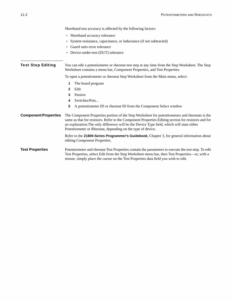
11-2 POTENTIOMETERS AND RHEOSTATS
e Step
is the and for
t
. To edit ith a
Shorthand test accuracy is affected by the following factors:
• Shorthand accuracy tolerance
• System resistance, capacitance, or inductance (if not subtracted)
• Guard ratio error tolerance
• Device-under-test (DUT) tolerance
Test Step Editing You can edit a potentiometer or rheostat test step at any time from the Step Worksheet. ThWorksheet contains a menu bar, Component Properties, and Test Properties.
To open a potentiometer or rheostat Step Worksheet from the Main menu, select:
1 The board program
2 Edit
3 Passive
4 Switches/Pots...
5 A potentiometer ID or rheostat ID from the Component Select window
Component Properties The Component Properties portion of the Step Worksheet for potentiometers and rheostatssame as that for resistors. Refer to the Component Properties Editing section for resistors an explanation.The only difference will be the Device Type field, which will state either Potentiometer or Rheostat, depending on the type of device.
Refer to the Z1800-Series Programmer’s Guidebook , Chapter 3, for general information abouediting Component Properties.
Test Properties Potentiometer and rheostat Test Properties contain the parameters to execute the test stepTest Properties, select Edit from the Step Worksheet menu bar, then Test Properties—or, wmouse, simply place the cursor on the Test Properties data field you wish to edit.
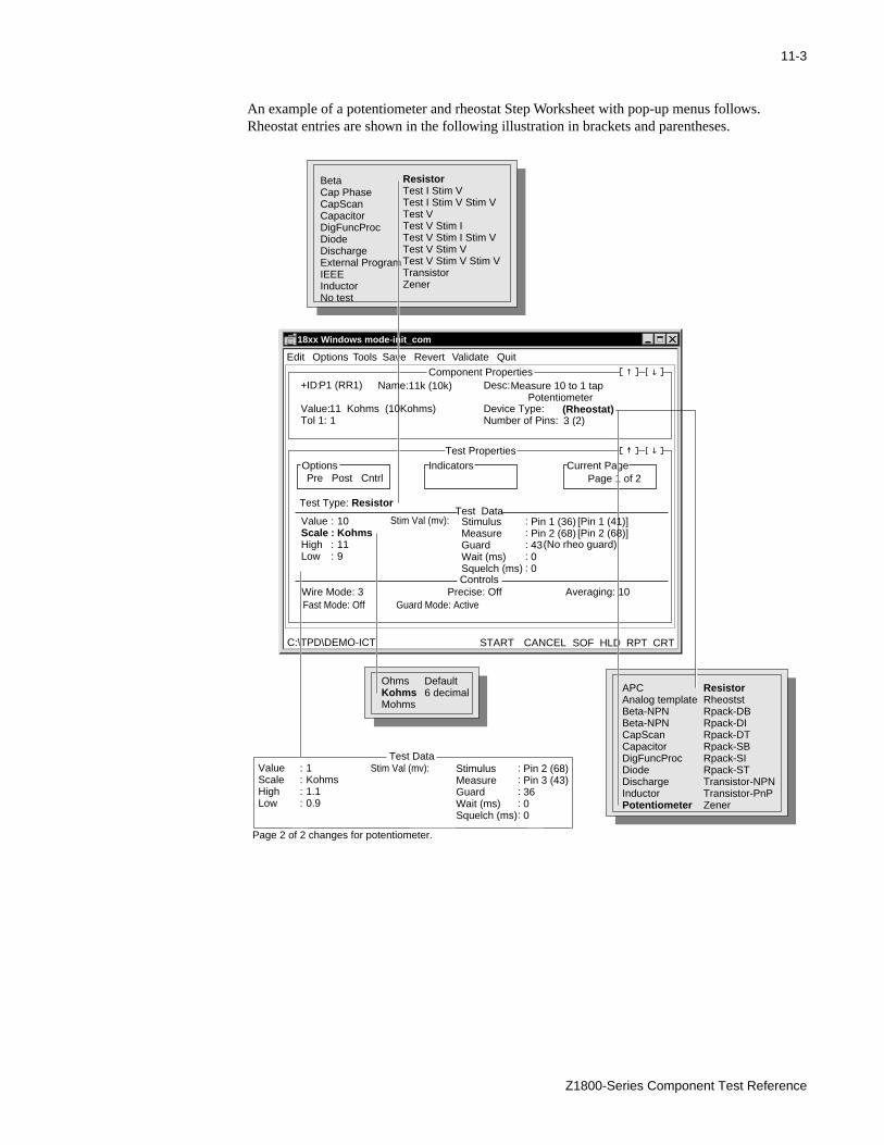
11-3
An example of a potentiometer and rheostat Step Worksheet with pop-up menus follows. Rheostat entries are shown in the following illustration in brackets and parentheses.
ValueScaleHighLow
1Kohms1.10.9
StimulusMeasureGuardWait (ms)Squelch (ms)
::::
:::::
Pin 2 (68)Pin 3 (43)3600
Test Data
Page 2 of 2 changes for potentiometer.
Stim Val (mv):
BetaCap PhaseCapScanCapacitorDigFuncProcDiodeDischargeExternal ProgramIEEEInductorNo test
ResistorTest I Stim VTest I Stim V Stim VTest VTest V Stim ITest V Stim I Stim VTest V Stim VTest V Stim V Stim VTransistorZener
18xx Windows mode-init_com
Page 1 of 2
Test Data
Controls
Edit Options Tools Revert Validate QuitSave
Component Properties
Test Properties Options Indicators
Pre Post CntrlCurrent Page
START CANCEL SOF HLD RPT CRT
Test Type: Resistor
C:\TPD\DEMO-ICT
Wire Mode: 3 Precise: Off Averaging: 10
APCAnalog templateBeta-NPNBeta-NPNCapScanCapacitorDigFuncProcDiodeDischargeInductorPotentiometer
ResistorRheoststRpack-DBRpack-DIRpack-DTRpack-SBRpack-SIRpack-STTransistor-NPNTransistor-PnPZener
+ID:
Value:Tol 1:
Name: Desc:
Device Type:Number of Pins:
P1 (RR1) 11k (10k)
(Rheostat)3 (2)1
Measure 10 to 1 tap Potentiometer
11 Kohms (10Kohms)
ValueScaleHighLow
10Kohms119
StimulusMeasureGuardWait (ms)Squelch (ms)
::::
:::::
Pin 1 (36)Pin 2 (68)4300
[Pin 1 (41)][Pin 2 (68)]
(No rheo guard)
Stim Val (mv):
OhmsKohmsMohms
Fast Mode: Off Guard Mode: Active
Default6 decimal
Z1800-Series Component Test Reference

11-4 POTENTIOMETERS AND RHEOSTATS
the ts and
anging
citors.
The Test Type field allows you to select an analog test configuration or test type to executestep. Test types can be either shorthand or longhand. The shorthand Test Type for rheostapotentiometers is Resistor. The longhand test types are Test V Stim I and Test I Stim V.
When you change test types, certain Test Properties fields also change, especially when chfrom shorthand to longhand.
The following fields function the same for potentiometers and rheostats as they do for capa
Refer to the Z1800-Series Programmer’s Guidebook , Chapter 3, for more information about the following fields.
High and Low Squelch
Stimulus Wire Mode
Measure Precise
Guard Higuard
Wait Averaging
Upper Test Properties Area
Field Description
Test Type: Type of test configuration used on current Step Worksheet. Recommended for inductors:
Resistor Shorthand potentiometer test
Test I Stim V Voltage stimulus and current measurement test
Test V Stim I Current stimulus and voltage measurement test
Test Data/Middle Test Properties Area
Value Numeric field specifying nominal expected value of Scale. Range = 0 – 999.
Scale: Value field's unit modifier based on Test Type.
Resistor Ohms, Kohms, Mohms
Test I Stim V na, ua, ma
Test V Stim I uv, mv, V

he ce the
ndard
and
ment the age o the
puting is . Use
12 RESISTORS
Resistor tests can be divided into two basic modes of testing—shorthand and longhand. Tshorthand mode is a component-specific test that offers the best possible performance sinsystem software can automatically make certain assumptions and corrections.
The shorthand test is done through the Resistor Test Type. It can be further divided into staresistor tests and extended resistor tests.
The PRISM-Z (PRecision Integrated Signal Measurement) module is available as an optioncan be used for Resistor tests. Refer to the Z1800-Series PRISM-Z User’s Guide for a complete discussion about the PRISM-Z test types available for Resistor tests.
Standard Resistor Test (Extended Off)
The following illustration shows a basic resistor shorthand test—3-wire, Precise of
Theory The ATB is setup for Test I Stim V mode that places the DUT in the input leg of the measureoperation amplifier (MOA). The summing junction at the F pole is held at virtual ground by output current of the MOA flowing through the selected computing resistor. The output voltof the MOA is proportional to the impedance of the DUT and is routed via scale selectors tA/D converter. Stimulus and measure types are always set to DC while the stimulus scale (stimulus voltage) depends on the expected value of the DUT. The Measure scale and comresistor are chosen in order to yield the most accurate measurement. The stimulus voltagenormally set to 200 mv except for target DUT values above 2 MΩ where it is set to1 V and valuesabove 20 MΩ where it is set to 10 V. Higher stimulus voltages can cause guarding problemsExtended Mode to control the stimulus voltage.
StimType
+
-MOA
+
-Stim
Guard-
+
Fd
Fs
Gd
Gs
Ed
Es
K159.935R82K1699.935R89K251KR84K2610KR91K35100KR86K361MR92K4510MR87K55
Computing Resistor
MeasScale
MeasType
MeasA/D
DC
DC
StimScale
Rg
Rg
DUT
(Stimulus)
(Measure)
(Guard)

12-2 RESISTORS
1.5 off. . For e UT e -Wire
Test accuracy is affected by the following factors:
• Shorthand system accuracy
• System resistance if not in 5/6-wire mode, Precise
• Guard ratio error
• Device-under-test (DUT) tolerance
Refer also to page 5 for more information about Extended Mode.
Refer also to the Resistor Range and Accuracy table in the Z1800-Series Maintenance Reference .
Effects of system resistanceThe Setup/Environment menu contains a field for system resistance with a default value ofOhms. This value is subtracted for all shorthand resistor tests done in 3-Wire with Precise The 1.5 Ohm is merely an average and is not necessarily correct for all node combinationsany other wire modes, or if Precise is enabled, the system resistance is corrected for by thmeasurement setup. Because of the increasingly unfavorable ratio between system and Dresistance for component values below 200 Ohms, 5- or 6-Wire mode and/or Precise modshould be used to test such components. The greatest accuracy can be obtained in 5- or 6mode with Precise on.
Resistor Test Step Editing
You can edit a resistor test step at any time from the Step Worksheet. The Step Worksheetcontains a menu bar, Component Properties, and Test Properties.
To open a resistor Step Worksheet from the Main menu, select
1 The board program
2 Edit
3 Passive
4 Resistors
5 A resistor ID (R2, for example) from the Component Select window
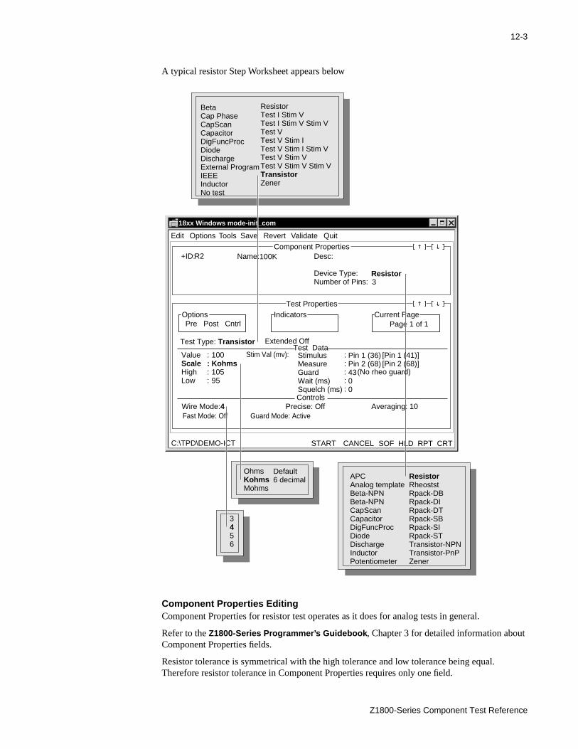
12-3
t
A typical resistor Step Worksheet appears below
Component Properties EditingComponent Properties for resistor test operates as it does for analog tests in general.
Refer to the Z1800-Series Programmer’s Guidebook , Chapter 3 for detailed information abouComponent Properties fields.
Resistor tolerance is symmetrical with the high tolerance and low tolerance being equal. Therefore resistor tolerance in Component Properties requires only one field.
BetaCap PhaseCapScanCapacitorDigFuncProcDiodeDischargeExternal ProgramIEEEInductorNo test
ResistorTest I Stim VTest I Stim V Stim VTest VTest V Stim ITest V Stim I Stim VTest V Stim VTest V Stim V Stim VTransistorZener
18xx Windows mode-init_com
Page 1 of 1
Test Data
Controls
Edit Options Tools Revert Validate QuitSave
Component Properties
Test Properties Options Indicators
Pre Post CntrlCurrent Page
START CANCEL SOF HLD RPT CRT
Test Type: Transistor
C:\TPD\DEMO-ICT
Wire Mode:4 Precise: Off Averaging: 10
APCAnalog templateBeta-NPNBeta-NPNCapScanCapacitorDigFuncProcDiodeDischargeInductorPotentiometer
ResistorRheoststRpack-DBRpack-DIRpack-DTRpack-SBRpack-SIRpack-STTransistor-NPNTransistor-PnPZener
+ID: Name: Desc:
Device Type:Number of Pins:
R2 100K
Resistor3
ValueScaleHighLow
100Kohms10595
StimulusMeasureGuardWait (ms)Squelch (ms)
::::
:::::
Pin 1 (36)Pin 2 (68)4300
[Pin 1 (41)][Pin 2 (68)]
(No rheo guard)
Stim Val (mv):
OhmsKohmsMohms
Fast Mode: Off Guard Mode: Active
Extended Off
3456
Default6 decimal
Z1800-Series Component Test Reference

12-4 RESISTORS
t
here ons
stances
t
gy of e
If you wish to alter the testing limits, do not modify the resistor tolerance field in ComponenProperties. Instead use the Tolerance Calculator menu to change the testing limits in Test Properties.
To open the Tolerance Calculator:
1 In the worksheet, double-click the Value, High, or Low fields.
The calculator shows the current worksheet values and tolerance. A field is available wyou can modify the high and low tolerances. Another field shows how your modificatiwill effect the worksheet values.
2 Select OK to accept the values or Cancel to exit the Tolerance Calculator.
Test Properties EditingTest Properties for resistor tests operates as it does for analog tests in general except for inlisted below in the table, Resistor Test Properties fields.
Refer to the Z1800-Series Programmer’s Guidebook , Chapter 3 for detailed information abouTest Properties fields.
Test Properties fields specific to resistor tests are described in the following table.
Fast Mode . The Fast option when set to ON suppresses built-in wait and squelch times for improved throughput. Depending on the expected value of the DUT, the system normally supplies default squelch and wait times that might not be needed depending on the topolothe board. When you enable Fast Mode, you must find appropriate wait and squelch timesyourself. While small wait times are often needed, squelch times are an issue only when thHiguard option is also selected.
Refer to the Z1800-Series Programmer’s Guidebook , Chapter 5, for a discussion of Higuard, Wait and Squelch times, Wire Mode, and Precise.
Upper Test Properties Area
Field Description
Test Type: Type of test configuration used on current Step Worksheet. Recommended Types for resistors follow below:
Resistor Shorthand resistor test.
Test I Stim V Voltage stimulus and current measurement test. (Preferred for resistor test. See Chapter 1, Shorthand and Longhand Theory.)
Test V Stim I Current stimulus and voltage measurement test.
Extended Enables extended shorthand test. Default is Off.
Test Data/Middle Test Properties Area
Value A numeric field specifying the nominal expected value of Scale. Range = 0 – 1000.000
Scale Value field’s unit modifier based on Test Type.
Resistor Ohms, Kohms, Mohms
Stim Val (mv) A numeric field to specify stimulus value in mv.Range = -750–+750 mv DC. Default = 200 mv.
Controls/Lower Test Properties Area
Fast Mode ON or OFF. Default is OFF. When ON, test runs without built-in Wait and Squelch times.
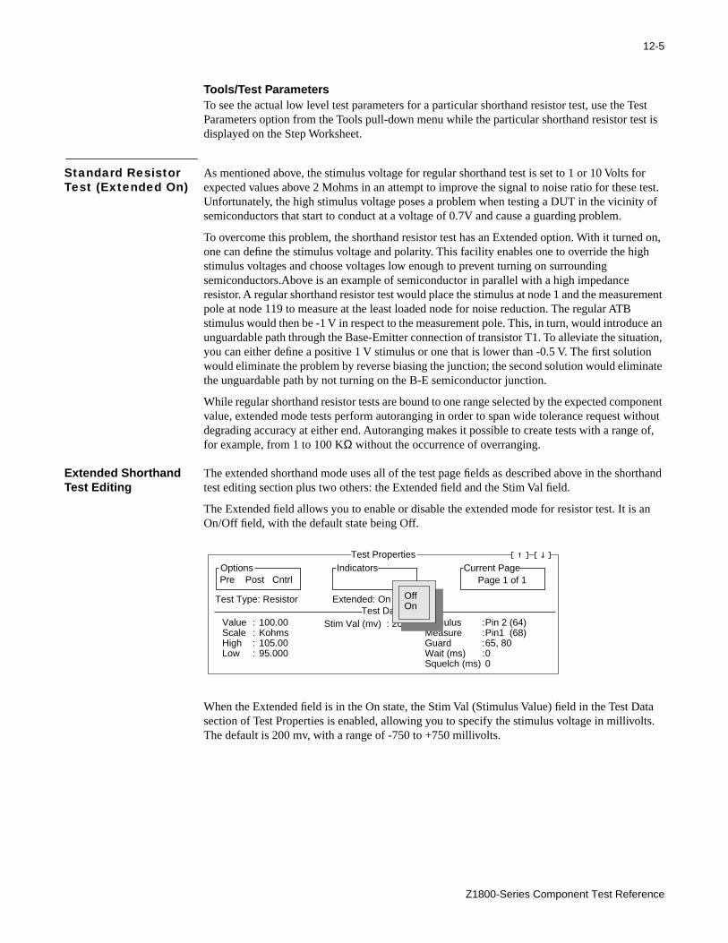
12-5
Test st is
for e test. y of
ed on, igh
rement ce an ation, ion inate
ponent ithout e of,
orthand
an
ata lts.
Tools/Test ParametersTo see the actual low level test parameters for a particular shorthand resistor test, use the Parameters option from the Tools pull-down menu while the particular shorthand resistor tedisplayed on the Step Worksheet.
Standard Resistor Test (Extended On)
As mentioned above, the stimulus voltage for regular shorthand test is set to 1 or 10 Volts expected values above 2 Mohms in an attempt to improve the signal to noise ratio for thesUnfortunately, the high stimulus voltage poses a problem when testing a DUT in the vicinitsemiconductors that start to conduct at a voltage of 0.7V and cause a guarding problem.
To overcome this problem, the shorthand resistor test has an Extended option. With it turnone can define the stimulus voltage and polarity. This facility enables one to override the hstimulus voltages and choose voltages low enough to prevent turning on surrounding semiconductors.Above is an example of semiconductor in parallel with a high impedance resistor. A regular shorthand resistor test would place the stimulus at node 1 and the measupole at node 119 to measure at the least loaded node for noise reduction. The regular ATBstimulus would then be -1 V in respect to the measurement pole. This, in turn, would introduunguardable path through the Base-Emitter connection of transistor T1. To alleviate the situyou can either define a positive 1 V stimulus or one that is lower than -0.5 V. The first solutwould eliminate the problem by reverse biasing the junction; the second solution would elimthe unguardable path by not turning on the B-E semiconductor junction.
While regular shorthand resistor tests are bound to one range selected by the expected comvalue, extended mode tests perform autoranging in order to span wide tolerance request wdegrading accuracy at either end. Autoranging makes it possible to create tests with a rangfor example, from 1 to 100 KΩ without the occurrence of overranging.
Extended Shorthand Test Editing
The extended shorthand mode uses all of the test page fields as described above in the shtest editing section plus two others: the Extended field and the Stim Val field.
The Extended field allows you to enable or disable the extended mode for resistor test. It isOn/Off field, with the default state being Off.
When the Extended field is in the On state, the Stim Val (Stimulus Value) field in the Test Dsection of Test Properties is enabled, allowing you to specify the stimulus voltage in millivoThe default is 200 mv, with a range of -750 to +750 millivolts.
Current PagePage 1 of 1
IndicatorsOptionsTest Properties
Test DataTest Type: Resistor Extended: On
ValueScale HighLow
::::
100.00Kohms105.0095.000
Stim Val (mv) : 200 StimulusMeasureGuardWait (ms)Squelch (ms)
::::
Pin 2 (64)Pin1 (68)65, 8000
Pre Post Cntrl
OffOn
Z1800-Series Component Test Reference

12-6 RESISTORS
st into the eds to
ls since s, an llel
em. is
keep ulus
es are duced rpret.
nd and
Resistors in Parallel with other Components
When resistors are in parallel with capacitors, the program generator copies the resistor tepage one of a two-page capacitor test in the Capacitor section. The original resistor test inresistor section is disabled but left in place for documentation purposes. The resistor test nebe done with the best accuracy possible by using averaging, precise and wire mode controit directly affects the outcome of the capacitor reading. For large paralleling capacitor valueincreasingly large wait time needs to be programmed during the resistor test to let the paracapacitor charge up before a measurement is taken.
See the Capacitor Test Type for more details on RC testing.
Resistors/Resistors
When resistors are in parallel with other resistors there is no way to electrically separate thThe only option is to measure the bulk impedance of the combination. The bulk impedancecalculated with the following formula:
where R total = Bulk impedance in OhmsR1 = R1 impedance in OhmsR2 = R2 impedance in Ohms
For more than 2 resistors the formula looks like this:
When resistors are in parallel with semiconductors, it is important to use extended mode tothe stimulus voltage below the semiconductor turn-on voltage of 0.7 V. Programing for stimvalues of less than 500 mv, generally prevents any semiconductors from conducting.
See also the discussion for Extended mode.
Longhand Testing of Resistors
Resistors can also be tested by using longhand Test Types TISV and TVSI. These test typprogrammed in generic units of volts and amperes. Because the diagnostic messages profor longhand tests are not based on DUT units of Ohms, failure diagnostics are hard to inte
Refer to Chapter 1, Shorthand and Longhand Theory, for a complete discussion of shorthalonghand testing.
R total R1 R2⋅R1 R2+--------------------=
1R_tot------------- 1
R1------- 1
R2------- 1
R3------- 1
Rn-------+ + +=

tion for
gh rties,
k
es the n the
t
ws in
13 RPACKS
Resistor packs (Rpacks) are tested as multipage resistors. Refer to the Resistor Tests secdetails regarding standard resistor test methods and Test Properties fields.
The Tol field for Rpacks is symmetric; that is, the low value tolerance is the same as the hivalue tolerance. Do not use this field to alter test limits. Alter test limits either in Test Propewith the tolerance calculator, or by direct entry of high and low limits.
The Device Type field offers the following choices for Rpack testing:
RPACK-DB Dual bus
RPACK-DI Dual in-line
RPACK-DT Dual terminator
RPACK-SB Single bus
RPACK-SI Single in-line
RPACK-ST Single terminator
Refer to the Z1800-Series Programmer’s Guidebook , Chapter 8, for illustrations of these Rpactypes.
The Number of Pins field defines the test generation process for the test step and configurNode Entry window with the correct number of pins. This field defines the number of pins odevice to which tester nodes will be connected. For Rpacks, enter as many as apply to thepackage type.
Rpack Test Step Editing
You can edit an Rpack test step at any time from the Step Worksheet. The Step Worksheecontains a menu bar, Component Properties, and Test Properties.
To access an Rpack Step Worksheet from the Main menu, select:
1 Edit
2 Passive
3 Rpacks
4 The Rpack ID from the Component Select window.
Rpacks are multipage resistor tests. To move through the pages, click the up or down arroTest Properties.

, two
forward urrent
ulus
nd ate for rent
and ard istor
. A istor
14 TRANSISTOR AND GAIN
Transistors are tested as two back-to-back diodes. Because transistors have two junctionsTest Properties pages are required—one for an emitter-base (E-B) diode test and one for acollector-base (C-B) test.
For PNP transistors, the anodes of the diode tests are the collector and emitter. For NPN transistors, the anodes are the base. Each Test Properties page (diode test) will measure avoltage drop in response to an injected forward current, and an optional reverse (leakage) cmeasure in response to an applied reverse voltage.
The figure below illustrates the equivalent circuit configurations for both NPN and PNP transistors. The forward voltage drop test places the transistor in the feedback loop of the measurement amplifier circuit. Reverse leakage tests place the transistor between the stimand the input to the measurement amplifier.
Transistor test circuit configuration diagram.
Testing Techniques Transistors with parallel semiconductor junctions or unguardable parallel paths are usuallyexamined for proper orientation only.
Transistor junctions with parallel unguardable resistors can be examined using the shorthaNPN or PNP statements; however, the measurement values must be modified to compensthe effects of the resistor. The test is possible because the transistor junction exhibits differesistance values depending on whether the junction is forward-biased or reverse-biased.
The forward voltage drop is usually lower because of current flow through both the resistorthe transistor junction. To compensate for current loss in the parallel component, the ForwCurrent (ma) can be increased to achieve the proper forward drop voltage across the transjunction. The reverse leakage current usually cannot be tested.
Unguardable parallel capacitors do not usually influence transistor junction measurementsdelay (wait state) can be added in parallel between stimulus application and measurementexecution so the capacitor can be charged to eliminate the capacitor current from the transmeasurement.
+
-
MEASUREMENTAMPLIFIER
D. COLLECTOR-BASE REVERSE LEAKAGE CURRENT
C. EMITTER-BASE REVERSE LEAKAGE CURRENTA. EMITTER-BASE FORWARD VOLTAGE DROP
B. COLLECTOR-BASE FORWARD VOLTAGE DROP
+
-
MEASUREMENTAMPLIFIER
Rc
+
-
MEASUREMENTAMPLIFIER
Vo
RcE
B
C
E POLE
F POLE
+
-
MEASUREMENTAMPLIFIER
Rc
Rc
E
B
C E POLE
F POLE
E
B
CE POLE
F POLE
++
+E
B
C
E POLE
F POLE
+

14-2 TRANSISTOR AND GAIN
ized es:
d e sitive sistors.
e is eping
d. zero
dely
istors. ons. r the , use
t for an e pole.
Field Effect Transistors
Like NPN or PNP transistors, which can be lumped into broad categories allowing generalstimulus and measurement parameters, FETs can also be lumped into two broad categoriJFETs, junction field effect transistors, and IGFETs, insulated gate field effect transistors.
There are many kinds of JFETs and IGFETs, each with different parameters for voltage ancurrent. Almost every device on the tested assembly must be individually examined and thunique stimulus and measurement values empirically determined. FETs are also more sento the components surrounding the printed circuit board assembly than NPN and PNP tran
Test V Stim I is normally used to test FETs while they are in the on state. The gate electrodguarded, forcing the device to switch on. The F pole is connected to the drain electrode, keit essentially at zero volts or virtual ground. The E pole is connected to the source lead.
An appropriate current Ic is applied to the drain electrode and the response voltage measureSince the JFET is essentially turned on, the expected response voltage should be close tovolts. A typical JFET source-drain voltage drop is approximately 0.3 volts.
The stimulus current required to force the source-drain voltage drop to zero volts varies widepending on the characteristics of the tested device. Values of Ic may vary between 0.1 mA and1.0 mA, with the acceptable stimulus value discovered during the programming debuggingprocess.
Acceptance limits also depend on the characteristics of the particular device-under-test. Generally, a source-drain voltage greater than 0.5 volts indicates a defective device.
Dual stimulus tests can be used to create a switch on test for active components.
Reversed Transistors and Beta Test
One of the more common assembly errors found on printed circuit boards is reversed transA 180° rotation of these transistors causes the collector and the emitter to exchange positiAssembly reversal will allow a transistor to pass the standard transistor test that checks foexistence of back-to-back diodes. If product history indicates a reversed transistor problemthe Beta (Gain) test to discover errors before board power is applied.
The Beta test requires special fixture wiring and node placement considerations to accountwo stimulus sources. The emitter must be on analog drive poles. The collector must be onanalog sense pole. The first 16 nodes on every driver/receiver board are on the analog drivThe second 16 nodes are on the analog sense pole.
The Beta test configuration appears below.
+
-Rc E
B
C
+
Rc2
+
Es
EdF

14-3
et
t values
Transistor Test Step Editing
You can edit a transistor test step at any time from the Step Worksheet. The Step Workshecontains a menu, Component Properties, and Test Properties.
To access a transistor Step Worksheet from the Main menu, select:
1 The board program
2 Edit
3 Semi
4 Transistors
5 A transistor ID (Q1, for example), from the Component Select window.
Component Properties Editing
Refer to the Z1800-Series Programmer’s Guidebook , Chapter 3, for a description of Component Properties fields.
Transistors, however, do not have value or tolerance fields because the reverse voltage tesare predetermined by the software and reported in Test Properties High and Low fields.
Z1800-Series Component Test Reference

14-4 TRANSISTOR AND GAIN
r
ave 3
Test Properties Editing
To edit a transistor Test Properties, select Edit from the menu bar, then Test Properties—osimply place the cursor on the data field you wish to edit. An example of a transistor Step Worksheet with pop-up menus appears below.
The following table describes the fields unique to transistor test. Transistor tests generally hpins contained on 2 Test Properties pages.
NoYes
18xx Windows mode-init_com
Page 1 of 1
Test DataTest Type: Capacitor
Edit Options Tools Revert Validate Quit
C:\TPD\DEMO-ICT
Save
Component Properties
Test Properties Options Indicators
Pre Post CntrlCurrent Page
START CANCEL SOF HLD RPT CRT
BetaCap PhaseCapScanCapacitorCapacitor (Prism)DigFuncProcDiodeDischargeExternal ProgramIEEEInductorInductor (Prism)No.TestResistor
Resistor (Prism)Test I Stim VTest I Stim V (Prism)Test I Stim V Stim VTest VTest V (Prism)Test V Stim ITest V Stim V (Prism)Test V Stim I Stim VTest V Stim VTest V Stim V (Prism)Test V Stim V Stim VTransistorZener
APCAnalog templateBeta-NPNBeta-PNPCapScanCapacitorDigFuncProcDiodeDischargeInductorPotentiometer
ResistorRheoststRpack-DBRpack-DIRpack-DTRpack-SBRpack-SIRpack-STTransistor-NPNTransistor-PnPZener
ControlsWire Mode: 3 Precise: Off Averaging: 1Guard Mode: Active
Test Type: Transistor
+ID: Name: Desc: NPN-Gain
Device Type:Number of Pins:
Q1B
Gain:120 Coll Curr: 0.000 ma
2222A
Transistor-NPN3
ScaleHighLowForward Curr (ma) : 10.000
mv840560
StimulusMeasureGuardWait (ms)Squelch (ms)
:::
:::::
Pin 2 (1)Pin 1 (9)
00
Reverse TestReverse Curr (ua)Stim Node On
:::
Yes1PNP-B/E
uvmvV
PNP-B/EPNP-E/BPNP-B/CPNP-C/BNPN-E/BNPN-B/ENPN-C/BNPN-B/C
Default6 decimal

14-5
Refer to the Z1800-Series Programmer’s Guidebook , Chapter 3, for further information about the Test Properties fields.
Upper Test Properties Area
Field Description
Test Type: The type of test configuration used on the current Test Properties page.
Transistor Shorthand transistor test
Beta Beta (gain) shorthand test. (See the following table.)
Test I Stim V Voltage stimulus and current measurement test. (See Longhand Analog section)
Test V Stim I Current stimulus and voltage measurement test. (See Longhand Analog section)
Test Data/Middle Test Properties Area
Scale (Transistor Test Type)
uv, mv, V
Forward Current (ma) Adjustable current value. Default 10 (ma)
Reverse Test YES or NO. When YES, performs reverse leakage test.
Reverse Curr (ua) When Reverse Test is YES, enter number from 0 to 999 (ua).
Stim Node On Anode or Cathode stim pole connection, to adjust polarity of forward drop and reverse leakage tests. Choices for NPN and PNP are: E/B–emitter/base (stim node on emitter); B/E–base/emitter (stim node on base); C/B–collector/base (stim node on collector); and B/C–base/collector (stim node on base).
Z1800-Series Component Test Reference

14-6 TRANSISTOR AND GAIN
An example of a transistor Beta Step Worksheet with pop-up menus appears below.
18xx Windows mode-init_com
Page 1 of 1
Test DataTest Type: Capacitor
Edit Options Tools Revert Validate Quit
C:\TPD\DEMO-ICT
Save
Component Properties
Test Properties Options Indicators
Pre Post CntrlCurrent Page
START CANCEL SOF HLD RPT CRT
BetaCap PhaseCapScanCapacitorCapacitor (Prism)DigFuncProcDiodeDischargeExternal ProgramIEEEInductorInductor (Prism)No.TestResistor
Resistor (Prism)Test I Stim VTest I Stim V (Prism)Test I Stim V Stim VTest VTest V (Prism)Test V Stim ITest V Stim V (Prism)Test V Stim I Stim VTest V Stim VTest V Stim V (Prism)Test V Stim V Stim VTransistorZener
APCAnalog templateBeta-NPNBeta-PNPCapScanCapacitorDigFuncProcDiodeDischargeInductorPotentiometer
ResistorRheoststRpack-DBRpack-DIRpack-DTRpack-SBRpack-SIRpack-STTransistor-NPNTransistor-PnPZener
ControlsWire Mode: 3 Precise: Off Averaging: 1Guard Mode: Active
GainTransisitor
120.000NPN
EmitterBase CollectorGuard
:::
::::
Pin 2 (1)Pin 1 (9)Pin 3 (68)
Collector CurrentScaleWait (ms)Squelch (ms)
::::
10ma00
Test Type: Beta
nauama
PNPNPN
+ID: Name: Desc: NPN-Gain
Device Type:Number of Pins:
Q1B
Gain:120 Coll Curr: 0.000 ma
2222A
Beta-NPN3
maA

14-7
ent. source
ting
e
ing oltage
s in
evice.
ester nt
The following table describes the fields unique to Beta test.
Refer to the Z1800-Series Programmer’s Guidebook , Chapter 3, for further information about the Test Properties fields.
The Beta test type uses both DC stimulus sources on the ATB to perform a beta measuremOne source is a constant voltage source on the collector, and the other a constant current on the base of the transistor.
You must specify the desired operating collector current in the Collector Current field from transistor specifications (found in data books), so the transistor is in the middle of its operarange, instead of at the saturation or cutoff point.
You must also specify the minimum acceptable gain or Hfe in the Gain field. This field is thminimum acceptable passing value.
Given the two inputs, Ic (desired Collector Current), and Hfe (Gain), the tester computes therequired Ib base current. The tester also selects the required stimulus voltages and computresistors for proper operation. The tester chooses values that put the collector-to-emitter vat approximately 3 volts.
With Ib applied and V measure sampled, the tester computes Ic. The tester will make up to 20 adjustment attempts, incrementing Ib base current each time until the Ic is approximately the requested Ic. The tester will increment in 20% positive and 10% negative steps until it homeon the requested Ic within a 5% of the requested Ic.
The tester takes a final measurement calculates the gain.
The Gain field represents the minimum acceptable gain for measurement on a transistor d
The Transistor field specifies whether the device is a PNP or NPN type of transistor. This information configures the test connections and stimulus polarities.
The Collector Current field allows you to specify the amount of collector current before the tcomputes the gain measurement. In other words, this entry specifies the gain measureme
Upper Test Properties Area
Field Description
Test Type: Beta The type of test configuration used on the current Test Properties page.Beta (gain) shorthand test
Test Data/Middle Test Properties Area
Gain Minimum acceptable gain for beta transistor measurement.
Transistor NPN or PNP
Collector Current Amount of beta collector current. Used with Gain to compute base current.
Scale na, ua, ma.
Wait (ms) 0 to 32000 ms. Added to default wait of 3 ms typical.
Squelch (ms) 0 to 32000 ms. Repeatable initial condition to remove stored energy.
Emitter Emitter pin/node number.
Base Base pin/node number.
Collector Collector pin/node number.
Guard Pin/node number(s) of the guard point(s). 10 nodes max.
Z1800-Series Component Test Reference

14-8 TRANSISTOR AND GAIN
se
field.
r.
operating point. With this value, plus the value in the Gain field, the tester computes the bacurrent for the test.
The Emitter field indicates the node number that connects to the transistor's emitter. If youautomatically generate the program, the software completes the field. You can also edit this
The Base field indicates the node number that connects to the base of the transistor.
The Collector field indicates the node number that connects to the collector of the transisto
I-1
INDEX
Aanalog test
accessing section 10-1test limits 1-1Test Type
Test V Stim V 1-6Test V Stim V Stim V 1-13
APC Threshold 6-4ATB longhand tests
Stim Types 1-6ATB specifications
RC testing 3-20auto-ignore
vector test 4-30
BBeta test
for reversed transistors 14-2for transistors 14-2
board powerediting Step Worksheet 2-1Mode field, programmable Test Properties 2-9nonprogrammable Scale field 2-6Power Prog test type fields 2-5power specification, digital test 2-1power specification, linear test 2-1Power test type fields 2-5
CCap Phase
capacitor test using 3-14measurements during capacitor testing 3-18test error messages 3-15Test Properties
Offset Cap 3-13Use Sys Cap 3-13
Test Properties test type 3-6test type specifications 3-20used with capacitor and RC tests 3-13
Cap Phase testfiguring system and offset capacitance 3-15specifying tolerance range 3-14Test Properties 3-13theory 3-12
capacitor specificationsEAA 3-16
capacitor testingAC/DC modes 3-2accessing Test Type modes 3-1ATB setup 3-2
autoranging in Extended mode 3-7basic modes 3-1Cap Phase functionality 3-1capacitor test using Cap Phase, tutorial 3-14capacitors smaller than 1000 pF 3-7capacitors smaller than 300 µF 3-2component ID block editing 3-5default system capacitance 3-3Discharge test step in capacitor section 3-4discharge test steps for special cases 6-1discharging capacitors 3-20editing Component Properties 3-5editing Test Properties 3-5erroneous failures 3-3Extended Analog Assembly (EAA) 3-8Extended shorthand test mode
theory 3-6Fast Mode 3-6inserting Discharge test 3-4longhand test mode 3-21
disadvantages 3-1preferred test type 1-9
measurements 3-18programming in TVSI mode 3-21RC Mode field 3-6residual charges 3-20shorthand accuracy 3-3shorthand test mode 3-1
theory 3-2squelch effects 3-6Step Worksheet editing 3-4suppressing wait and squelch times 3-6Test Properties
Cap Phase 3-13Cap Phase Test Type 3-6editing 3-5Extended field 3-6longhand test mode 3-22Test Type field 3-6
test type functionality 3-1test type theory 3-2testable range 3-3Tolerance fields 3-5V_dut Pk–Pk field 3-8viewing actual test parameters 3-7wait times
effects 3-6longhand test mode 3-22
Circuit Offset (pf) 3-13Close Analog Measure
removing window 4-31
Spectrum 8800-Series Test Development Reference
I-2
comparators, linear testing 9-1Component Properties 3-5
capacitor test editing 3-5diode testing 5-3discharge test
editing 6-1zener testing 5-3
continuity testing 8-1Component Properties 8-1Device Type fields 8-1expected continuity 8-1measurement threshold 8-1Step Worksheet
accessing 8-1editing 8-2
Test Propertiesediting 8-2
Test Type field 8-2Threshold field 8-2
Countwhen to use in Gray code test 4-9
CRCconditions affecting CRC measurement 4-8Gray code testing 4-8when to use 4-8when to use in Gray code test 4-8
Cyclic Redundancy Check. See CRC See also Gray code
DD/R boards, digital measurement 4-2defaults
Board Power wait 2-5capacitor RC mode 3-6capacitor test, Fast Mode 3-6continuity measurement 8-2continuity measurement threshold 8-1digital
duty cycle control 4-3software timeout 4-2termination resistors 4-2
digital test controlsclock source 4-31
diode test 5-2Gray code
clock divisor 4-17double coverage bursts 4-3From, To, While 4-3high threshold 4-17logic level 4-17low threshold 4-17programmable clock rate 4-4
Gray code measurement window 4-9
jumper measurement threshold 8-3linear wait 9-3, 9-4longhand analog wait 1-6, 1-8, 1-11, 1-13, 1-14, 1-15shorts measurement threshold 8-4system capacitance 3-3transistor Beta wait 14-7transistor forward current 14-5vector editor
logic level 4-31markers 4-22
zeners, current stimulus value 5-3DIALCO 521-92303 LED, parameters 5-2differential measurements
specifying ground reference node 1-4suppressing 1-4
digital guardingadding guard pins to vector test 4-25
digital testanalog-only system
digital testlogic signals 4-1
behavior of disables 4-13duty cycle control 4-3editing Stim Type and Stim Frequencies 4-7Gray code stimuli, when to use 4-1measurement methods 4-1mixed mode Gray code test 4-32
analog measure 4-37analog stimulus 4-37measure 4-33stimulus 4-34wait time 4-37
mixed mode vector test 4-38measure 4-38stimulus 4-40
opening the Step Worksheet 4-15specifications
D/R boards, digital measurement 4-2duty cycle control 4-3non-multiplexed stimulus 4-1programmable threshold reference 4-2software features 4-2termination resistors 4-2
theory 4-1vector patterns, when to use 4-1vector specifications 4-11
diode testinganalog measurement configuration 5-1Component Properties 5-3defaults 5-2determining type 5-2editing 5-3forward-biased voltage drop test 5-1

I-3
germanium device 5-2range of values 5-3Reverse Test field 5-8reverse-biased current leakage test 5-1shorthand stimulus 5-3shorthand test accuracy 5-3silicon device 5-2Step Worksheet
accessing 5-3example 5-4
Stim Node On field 5-8Test Properties, table 5-5Test Type field 5-7theory 5-1
disable tableduplicate nodes 4-13
disable Test Step 3-5discharge test step
adding APC test step to discharge 6-1Component Properties
editing 6-1danger of residual charges 6-1purpose 6-1Step Worksheet 6-2Test Properties
editing 6-1Test Type field 6-3Timeout field 6-3using Global APC for board contact 6-3
Display Analog Measuremonitoring test set up 4-31
DRAMs, testing with Gray code 4-10dual stimulus test modes
Test I Stim V Stim V 1-14Test V Stim I Stim V 1-15theory 1-11
duplicate nodes, checking for 4-13
EEAA
capacitor specifications 3-16capacitor/resistor specifications 3-16effects on capacitor and RC testing 3-8measurement technique 3-12RC-Phase board 3-8
enable Test Step 3-5enable/disable Test Step 3-5environmental capacitance, determining 3-15Extended Analog Assembly. See EAAextended shorthand test mode
autoranging in capacitor test 3-7editing 3-8Test Properties 3-8
Ffailure reporting
vector test 4-24failures
erroneous on large capacitors 3-3fixture verification, opens testing 8-4
GGain test. See Beta test. See also transistor testingGlobal APC
creating test step 6-4method to test for uncontacted nodes 6-3when to use in Discharge section 6-3
Gray codehigh threshold 4-17low threshold 4-17
Gray code frequenciesstimulus 4-4
Gray code test philosophy 4-1Gray code testing
characteristics 4-3clock ticks 4-3common timing origin 4-3easily visible markers 4-3No simultaneous transitions 4-3repeatable logic path 4-3
device size constraints 4-4Digital Measure window 4-20Digital Stimulus window 4-19
Connect/Disconnect field 4-20Digital Stimulus window, Comp field 4-19disable table duplicate nodes 4-13double coverage bursts 4-3DRAM 4-10Gray code groups, definition 4-18hardware timeout 4-4High, when to use 4-9Measurement enable timing 4-3measurement modifiers 4-10measurement types 4-3, 4-8
Count 4-9CRC 4-8High 4-9
measurement window 4-9memory device testing 4-10mixed mode 4-32mixed mode properties 4-4pattern depth 4-3Pin Record window 4-17Pin Type 4-18programmable clock rate 4-4SRAM 4-10stimulus example (MSI test) 4-8
Spectrum 8800-Series Test Development Reference

I-4
Test Properties 4-16using Comp field for Exclusive-Or 4-19validating stability of stimuli 4-6
HHiguard
resistor testing 12-4homing loops
adding a homing loop 4-26defining range 4-27deleting 4-28initializing devices to known state 4-26listing 4-28overlap 4-27window 4-27
IIGFET testing. See transistor testingignores testing 8-3
preventing false shorts reporting 8-3Step Worksheet
editing 8-3Threshold field 8-3
impedance ratioRC testing 3-17
inductor testing 7-1Component Properties 7-2Ignore groups for low resistance 7-1measuring DC resistance 7-1shorthand test accuracy 7-1Step Worksheet
editing 7-1Test Properties
editing 7-2Test Type field 7-3
interconnect testing 8-1
JJFET testing. See transistor testingjumper testing 8-3
different from continuity 8-3measurement threshold 8-3Step Worksheet
editing 8-3
LLearn Cap Phase Offsets 3-13Learn Expect Data 4-30LED testing 5-1linear testing 9-1
Device Type field 9-1longhand accuracy 9-1
shorthand accuracy 9-1Step Worksheet
accessing 9-1editing 9-2
Test TypeTest V 9-3Test V Stim V 9-3Test V Stim V Stim V 9-4
logic levelspecifying power supply in Gray code test 4-17specifying power supply in vector test 4-31
longhand test modeconverting shorthand test to 3-23differential measurements 1-3dual stimulus modes 1-11Test I Stim V 1-10Test V 1-2Test V Stim I 1-7Test V Stim I Stim V 1-15Test V Stim V 1-5theory 1-1wait time 1-3wait times 3-22
Mmeasurement modifier
WHILE 1 4-10measurement modifiers
FROM 4-10TO 4-10WHILE 2 4-10
measurementscapacitor testing 3-18
Merge_SC testing 8-4summary table function 8-4testing nodes for shorts 8-4
merge_SC testing 8-4mixed mode
analog effect on digital measurement 4-2modifying for Meas V test 4-33modifying for Stim V test 4-34modifying Gray code test 4-32modifying vector test 4-38pole assignment 4-14stimulus/measurement properties 4-4vector measure test 4-38vector stimulus test 4-40
MultiScan testingaccessing test category 10-1

I-5
Nnode group connectivity, verifying 8-1non-multiplexed stimulus, digital testing 4-1NPN testing. See transistor testing
OOffset Cap
Test Properties field 3-16offset capacitance, determining 3-16op amp testing
comparators 9-1linear testing 9-1
opens testing 8-4fixture verification 8-4Step Worksheet
accessing 8-5using shorting plate 8-4
Ppattern depth, vector test 4-11PNP testing. See transistor testingpotentiometer testing 11-1
Component Propertiesediting 11-2
shorthand test accuracy 11-2Step Worksheet
accessing 11-2editing 11-2example 11-3
Test Propertiesediting 11-2
Test Type field 11-4theory 11-1
Power Off longhand testing 10-1power off testing. See analog testingpower supplies
controlling A and B 2-6controlling DUT 5 V 2-6, 2-11controlling DUT 5.5 V 2-9controlling Power Prog Slaved 2-10using 12 V together 2-6using 15 V together 2-6verifying programmable supplies 2-8
Power Test Propertiescontroller requirements 2-1editing nonprogrammable 2-6editing programmable 2-8nonprogrammable 2-1nonprogrammable example 2-3Prog 5.5 V worksheet 2-9programmable 2-1programmable example 2-4relation to power supplies 2-9
Power Test Types±12 V and ±15 V 2-7A Adjustable, B Adjustable 2-8Power 2-5Power Prog 5.5V 2-5Power Prog B 2-5Power Prog Slaved 2-5relation to power supplies 2-7
PRISM-Z test types 1-1Capacitor 3-1Inductor 7-1Resistor 12-1
programmable threshold reference, digital testing 4-2
RRC testing
ATB specifications 3-20Cap Phase test type specifications 3-20debugging 3-17impedance ratio 3-17low value capacitors 3-20theory 3-17using Cap Phase Test Type 3-9
RC-Phase boardtesting small capacitors 3-8testing small RC combinations 3-8
relayslinear testing 9-1
resistor pack. See Rpackresistor testing
ATB setup 12-1autoranging 12-5basic modes 12-1Component Properties 12-3defining stimulus voltage and polarity 12-5effects of system resistance 12-2extended mode 12-5Fast Mode 12-4in parallel with another resistor 12-6in parallel with capacitors 12-6in parallel with semiconductors 12-6longhand test mode 12-6preferred longhand mode 1-11shorthand mode 12-1shorthand resistor test (extended mode) 12-5standard resistor tests 12-1Step Worksheet
accessing 12-2example 12-3
Test Propertiesediting 12-4
theory 12-1Tolerance Calculator 12-4
Spectrum 8800-Series Test Development Reference

I-6
viewing low level test parameters 12-5resistor/capacitor testing. See RC testingrheostat testing 11-1Rpack
Test Propertiesexample 13-1
Rpack testing 13-1Device Type field 13-1Number of Pins field 13-1Step Worksheet
accessing 13-1
Sshorthand test mode
converting to longhand 3-23theory 1-1
shorting plate, using in opens testing 8-4shorts testing 8-4
specifications 8-4Step Worksheet
accessing 8-4Threshold field 8-4
six decimal precision test limits 1-1specifications
ATB, RC testing 3-20Squelch time
zener testing 5-8
SRAMs, testing with Gray code 4-10Step Worksheet
Beta transistor 14-6capacitor 3-4
Discharge 3-4potentiometer and rheostat 11-3resistor test 12-3Test Properties
Test V Stim V 1-5Test V Stim V Stim V 1-12
Vector 4-21Stim Types for ATB longhand tests 1-6system capacitance
determining environmental capacitance 3-15
Ttermination resistors
digital testing 4-2Test I Stim V
Test Properties 1-10Test Type 1-11testing resistive components 1-11
Test I Stim V Stim V Test Properties fields 1-14test limits
six decimal precision 1-1
test memory devicesGray code 4-10
test methods, vector 4-12Test Properties
Cap Phase 3-13Cap Phase test type 3-6capacitor
Extended field 3-6test type 3-6
capacitor test editing 3-5Learn Cap Phase Offsets 3-13Offset Cap 3-13, 3-16potentiometer and rheostat 11-2resistor 12-4Rpack 13-1Test V Stim V 1-5Test V Stim V Stim V 1-12Use Sys Cap 3-13
Test Stepenable/disable 3-5
Test TypesAPC 6-5Beta 14-5Cap Phase
functionality 3-1Capacitor
functionality 3-1Continuity 8-2Diode 5-5Discharge 6-3Inductor 7-3linear analog test 9-3potentiometers and rheostats 11-4Power 2-6Resistor 12-4Transistor 14-5zener 5-7
Test Vautoranging 1-4longhand test mode 1-2measure modes 1-3Test Type 1-3worksheet 1-2
Test V Stim IATB setup 1-7compared to Test I Stim V 1-9compatible stimulus and measure 1-9for capacitive test 1-9hundred volt amplifier 1-9no autoranging 1-9Test Properties 1-8Test Type 1-8
Test V Stim I Stim VTest Type 1-15
I-7
Test V Stim VATB setup 1-5autoranging 1-7longhand test mode 1-5squelch time 1-6stimulus current limit 1-6stimulus greater than 10 V 1-6stimulus impedance 1-6stimulus magnitude and type 1-6Test Properties 1-5Test Type 1-6
Test V Stim V Stim Vlonghand test mode 1-12Test Properties 1-12Test Type 1-13
Tolerance Calculatorresistor testing 12-4
tolerance range, Cap Phase test 3-14transistor testing 14-1
Base field 14-8beta (Gain) test 14-2Beta Test Type 14-7Collector Current field 14-7Component Properties 14-3Emitter field 14-8Gain field 14-7IGFETs 14-2JFETs 14-2NPN transistors 14-1PNP transistors 14-1reversed transistors 14-2Step Worksheet
accessing 14-3Beta 14-6editing 14-3example 14-4
Test Propertiesediting 14-4
testing techniques 14-1
Uunit multipliers/scales used in 18xx software viiUse Sys Cap 3-13
Vvector clock 4-12vector editor
Add Guards window 4-25Auto-Ignore for failing vectors 4-30Close Analog Meas field 4-31Compress command 4-24Data Character window 4-28Delete States 4-25
digital test controlsClock Divisor 4-31Clock Source 4-31High Threshold 4-31Low Threshold 4-31Measurement Delay 4-31Terminators 4-31
Disp Analog Meas field 4-31Edit command 4-24Edit Unused Pin window 4-28Insert States command 4-25manipulating vector data patterns 4-23markers 4-22Modify command 4-25Modify Data Characters 4-24Next, advance to next failing state 4-24Pin Record window
Assigned Pole 4-23Learn Expect Data field 4-23, 4-30Trigger function 4-23
Pins window 4-22Prev, return to previous failing state 4-24Remove Guards window 4-26Repeat function 4-24Save 4-24Statistics command 4-29Status window 4-22Stop On Fail function 4-24Test_Config, digital test control 4-31Tools menu 4-29Vector Data window 4-23
Vector Performanceoption 4-12
Vector Processorcontroller board 4-12
vector processormeasurement clock 4-14stimulus clock 4-14
vector test 4-30analog stimulus and measurement effect on pole assignments 4-15applying deep vector patterns 4-12assessing quality of test 4-29auto-ignore 4-30changing failing states to don't care 4-30determining stable results 4-24device size constraints 4-11dual threshold effect on measurement 4-15effect of PC on compression time 4-24expanding Test Properties page 4-21failure reporting 4-24Fault Inject 4-29global response failure register 4-14map memory 4-13
Spectrum 8800-Series Test Development Reference

I-8
maximizing memory efficiency 4-12measurement enable timing 4-11pattern depth 4-11pole assignments 4-14priming pins 4-12processing digital response signals 4-13programmable clock rate 4-11programming listen window 4-14properties 4-11setting up row assignments 4-22specifying pin type 4-22statistical report 4-29Statistics report for pin activity 4-29Step Worksheet 4-21theory 4-12using test controls to analyze data 4-24vector clock 4-12vector compression 4-24vector editor 4-22
vector test philosophy 4-1Vector testing
disable table duplicate nodes 4-13voltage regulators, linear testing 9-1
WWaveScan testing
accessing test section 10-1write-back caching, erroneous failures 3-3
Zzener testing 5-1, 5-3
adding discharge test step 5-3Component Properties 5-3editing 5-3Forward Test field 5-7Forward Volt field 5-7maximum voltage if zener is missing 5-3range of values 5-3shorthand stimulus 5-3shorthand test accuracy 5-3Squelch time 5-8Step Worksheet
accessing 5-3example 5-6
Stim Node On field 5-8Test Properties, table 5-7Test Type field 5-7Value field 5-7