complete start guide: ni digital minisystem (dms) mydaq… startup 2014… · ·...
TRANSCRIPT

© 2014 Project Lead The Way, Inc. Start Guide: NI Digital MiniSystem – myDAQ; myDigital Protoboard; CmodS6 FPGA Module – Page 1
Complete Start Guide: NI Digital MiniSystem (DMS) myDAQ; myDigital Protoboard; Cmod S6 FPGA Module
Digilent Revision: August 13, 2013 Author: Marshall Wingerson PLTW Revision: October 25, 2013 Author Jason Rausch
NI Digital MiniSystem (RevB)
This is a guide on how to start using the Digital MiniSystem. The Digital MiniSystem is made up of three development tools; myDAQ, myDigital Protoboard, and the Cmod S6 FPGA Module. These instructions support the installation of software for use of both Digital MiniSystem and the Digital Logic Board in the DE classroom.
© 2014 Project Lead The Way, Inc. Start Guide: NI Digital MiniSystem – myDAQ; myDigital Protoboard; CmodS6 FPGA Module – Page 2
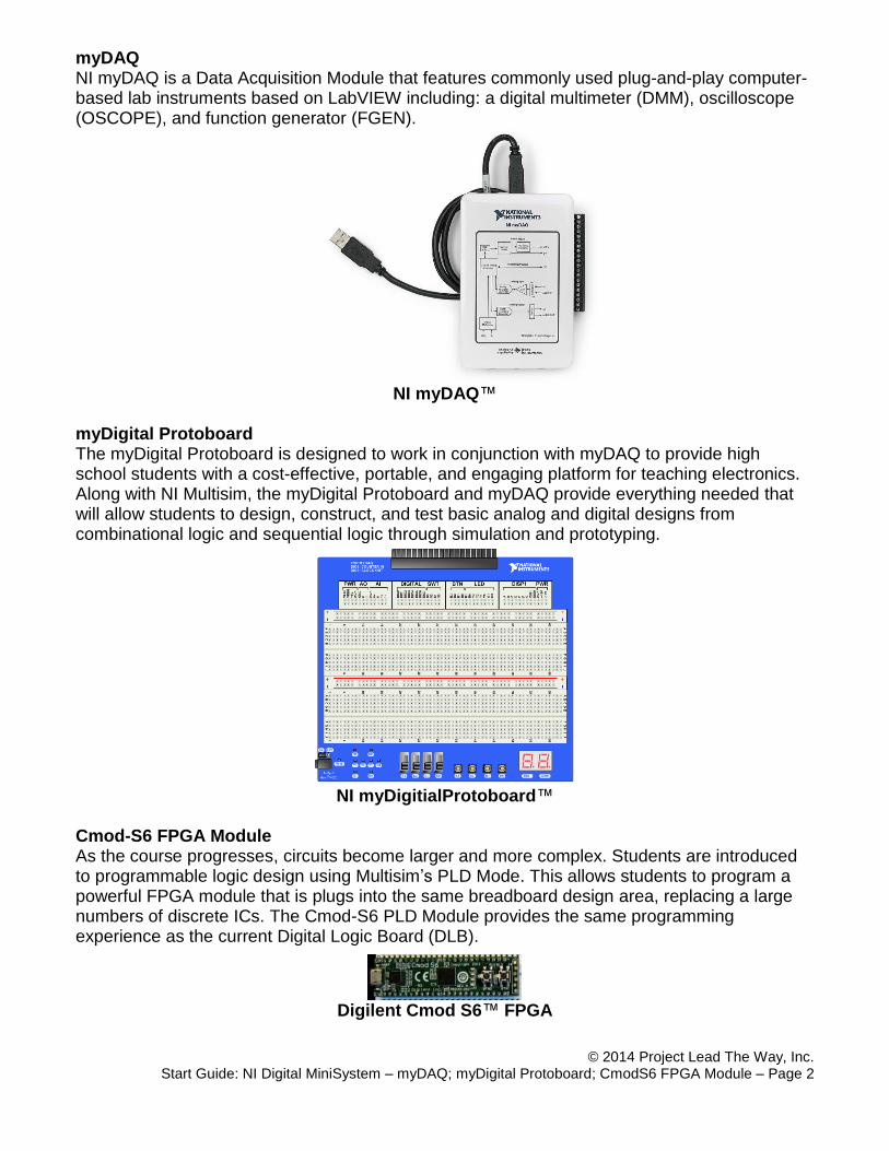
myDAQ NI myDAQ is a Data Acquisition Module that features commonly used plug-and-play computer-based lab instruments based on LabVIEW including: a digital multimeter (DMM), oscilloscope (OSCOPE), and function generator (FGEN).
NI myDAQ™
myDigital Protoboard The myDigital Protoboard is designed to work in conjunction with myDAQ to provide high school students with a cost-effective, portable, and engaging platform for teaching electronics. Along with NI Multisim, the myDigital Protoboard and myDAQ provide everything needed that will allow students to design, construct, and test basic analog and digital designs from combinational logic and sequential logic through simulation and prototyping.
NI myDigitialProtoboard™
Cmod-S6 FPGA Module As the course progresses, circuits become larger and more complex. Students are introduced to programmable logic design using Multisim’s PLD Mode. This allows students to program a powerful FPGA module that is plugs into the same breadboard design area, replacing a large numbers of discrete ICs. The Cmod-S6 PLD Module provides the same programming experience as the current Digital Logic Board (DLB).
Digilent Cmod S6™ FPGA

© 2014 Project Lead The Way, Inc. Start Guide: NI Digital MiniSystem – myDAQ; myDigital Protoboard; CmodS6 FPGA Module – Page 3
Required Hardware:
Computer with Software Installed
National Instruments myDAQ with USB
National Instruments myDigital Protoboard
Cmod S6 FPGA Module
Micro-USB B Cable
22 Gauge Solid Wire
Required Software Overview:
The following is a brief overview of the required software. Detailed installations begin on the next page.
NI myDAQ Software Suite 4.4 (Found on install disc accompanying NI myDAQ)
Install “Multisim 12.0”
- Single User Disc Install – Multisim 12.0 can be installed from the disc that comes with NI myDAQ and updated to “Multisim 12.0.1” from the NI Update Service.
- Single User Disc Install – Serial Number (S/N) to activate Multisim is located on the clear envelope that contains the white install disc envelope.
- Classroom Install – For instructions on preparing the classroom install of Multisim 12.0.1 please visit the PLTW Virtual Academy.
Install NI ELVISmx 4.4 Driver
- Single User Disc Install – NI myDAQ Software Suite 4.4 can be installed from the disc that comes with NI myDAQ.
NO INSTALL of LabVIEW 2012 is required to use the NI myDAQ. Install of LabVIEW 2012 is optional and not required for DMS use.
Install “NI LabVIEW FPGA Xilinx 12.4 SP1 Tools” Visit:
http://download.ni.com/evaluation/labview/ekit/other/downloader/2011SP1Xilinx124_downloader.exe
Note: “NI LabVIEW FPGA Xilinx 12.4 SP1 Tools” is utilized for both hardware platforms. (Digital Logic Board and Digital MiniSystem)

© 2014 Project Lead The Way, Inc. Start Guide: NI Digital MiniSystem – myDAQ; myDigital Protoboard; CmodS6 FPGA Module – Page 4
Detailed Xilinx 12.4 Installation Instructions
The following instructions describe the installation process for Xilinx 12.4 use with both the Digital Logic Board and the new Digital MiniSystem in the same classroom. Each board (DMS and DMS) require different drivers. Xilinx does not currently support Windows 8.
1. Detailed instructions for setting up a classroom image to clone can be found on the PLTW Virtual Academy (VA). http://www-old.pltw.org/moodle/course/view.php?id=167
2. Click here to install “NI LabVIEW FPGA Xilinx 12.4 SP1 Tools”. This will provide you
with the NI Downloader executable.
3. Run “2011SP1Xilinx124_downloader”.
4. Select: “Install NI LabVIEW FPGA Xilinx 12.4 SP1 Tools”

© 2014 Project Lead The Way, Inc. Start Guide: NI Digital MiniSystem – myDAQ; myDigital Protoboard; CmodS6 FPGA Module – Page 5
5. Installation Process: “NI LabVIEW FPGA Xilinx 12.4 SP1 Tools”
6. After installation of “NI LabVIEW FPGA 12.4 SP1 Tools” Select: Next
7. Fill out the following fields: Full Name: Organization: Select: “Install LabVIEW 2011SP1 Xilinx Tools Evaluation – Serial number not required”

© 2014 Project Lead The Way, Inc. Start Guide: NI Digital MiniSystem – myDAQ; myDigital Protoboard; CmodS6 FPGA Module – Page 6
8. Uncheck box to contact NI and search for updates. You will update after install and activation of “NI LabVIEW FPGA 12.4 SP1 Tools” Select: Next
9. Select: I accept the above 4 License Agreements Select: Next
10. Select: Next

Unpublished work © 2013 Project Lead The Way, Inc. Start Guide: NI Digital MiniSystem – myDAQ; myDigital Protoboard; CMODS6 PLD Module – Page 7
11. Select: Finish
12. You will need to restart your computer.
13. “Xilinx 12_4” is now located in the following folder location “C:NIFPGA”

Unpublished work © 2013 Project Lead The Way, Inc. Start Guide: NI Digital MiniSystem – myDAQ; myDigital Protoboard; CMODS6 PLD Module – Page 8
Xilinx 14.4 Update Instructions
14. To add the update “LabVIEW 2013 FPGA Module Xilinx Tools 14.4” using the NI Update Service:
Open: NI Update Service Navigate to: “Start” -> “All Programs” -> “National Instruments” Select: “NI Update Service”
15. Select: “LabVIEW 2013 FPGA Module Xilinx Tools 14.4”
Select: Install
16. Some Schools might block the NI Update Service. You can download and install directly from here: LabVIEW 2013 FPGA Module Xilinx Tools 14.4”

Unpublished work © 2013 Project Lead The Way, Inc. Start Guide: NI Digital MiniSystem – myDAQ; myDigital Protoboard; CMODS6 PLD Module – Page 9
Installing Drivers for the Cmod S6 FPGA Module
The following instructions describe the process to download (2) driver files needed to operate the Cmod S6 FPGA Module with Multisim, Xilinx, and your computer. The Digilent plugin_v2.6.3 will provide you with the correct .cse file and install Adept software, giving you access to the correct driver.
17. Download: Digilent.cseplugin_v2.6.3
18. Select: Run
19. Select: Next

Unpublished work © 2013 Project Lead The Way, Inc. Start Guide: NI Digital MiniSystem – myDAQ; myDigital Protoboard; CMODS6 PLD Module – Page 10
20. Select: I Agree
21. Check Boxes: “Adept Runtime” and “Digilent CsePlugin”
Select: Next
22. Uncheck Box: Create Quick Launch Shortcuts

Unpublished work © 2013 Project Lead The Way, Inc. Start Guide: NI Digital MiniSystem – myDAQ; myDigital Protoboard; CMODS6 PLD Module – Page 11
23. Select: Install
24. Select: Next
25. Select: Finish
26. All necessary software has been installed for Digital MiniSystem use.

Unpublished work © 2013 Project Lead The Way, Inc. Start Guide: NI Digital MiniSystem – myDAQ; myDigital Protoboard; CMODS6 PLD Module – Page 12
Adding Multisim Configuration and User Constraint Files
27. Download and unzip the folder containing the Digital MiniSystem Configuration Files.
“Digilent C-Mod S6.mspc”
“Digilent C-Mod S6.ucf”
28. Navigate to:
C:\Program Files(x86)\National Instruments\Circuit Design Suite 12.0\pldconfig
29. Copy the (2) files to the pldconfig folder.

Unpublished work © 2013 Project Lead The Way, Inc. Start Guide: NI Digital MiniSystem – myDAQ; myDigital Protoboard; CMODS6 PLD Module – Page 13
Testing Configuration of the Digital MiniSystem All answer keys and PLD Mode simulations related to the Digital MiniSystem will use these assigned pins. The myDigital Protoboard has been wired to be powered from the myDAQ.
It is highly recommend that VEXT, +15V, -15V be blocked off with a loop of wire (as shown) so that students do not exceed 5V on the CMODS6 PLD Module.
DO NOT WIRE VEXT, +15V, -15V TO THE PLD MODULE. The CMODS6 will fail above 5V. Cmod S6 – myDigital Protoboard PIO14 – DIO3 (CLK from myDAQ) PIO24 – VCC PIO25 – GND PIO26 – G PIO27 – F PIO28 – E PIO29 – D PIO30 – C PIO31 – B PIO32 – A PIO33 – DIG 0 PIO34 – DIG 1 PIO35 – G0 PIO36 – G1 PIO37 – Y0 PIO38 – Y1 PIO39 – Y2 PIO40 – Y3 PIO41 – R0 PIO42 – R1 PIO43 – B0 PIO44 – B1 PIO45 – S0 PIO46 – S1 PIO47 – S2
PIO48 – S3 myDigital Protoboard with Cmod S6 FPGA Module

Unpublished work © 2013 Project Lead The Way, Inc. Start Guide: NI Digital MiniSystem – myDAQ; myDigital Protoboard; CMODS6 PLD Module – Page 14
Powering the myDigital Protoboard
There are two options for powering the MyDigital Protoboard.
30. myDAQ as power source – With the MyDigital Protoboard coupled to the myDAQ +5V is supplied from the +5V PWR located at the top left of the board.
31. VEXT as power sourse (17V Max external battery or AC/DC adaptor) – When not tethered to the myDAQ, the MyDigital Protoboard can be powered by jumping from VREG to +5V PWR located at the top left of the board. The VEXT is a standard coaxial power connector (5.5mm X 2.1mm) commonly available on DC wall adapters (max 17VDC).
Powered by myDAQ Powered by External Voltage (17VMax)
32. Micro-USB B cable to power the PLD Module – The CMODS6 PLD Module can be powered with the PLD module tethered to a computer alone. However, the myDigital Protoboard must still be powered from Option #1 (myDAQ) or Option #2 (VEXT) if you wish to use the buttons or switches. The seven segment display will also appear dim as they are not being powered by 5V.
Unpublished work © 2013 Project Lead The Way, Inc. Start Guide: NI Digital MiniSystem – myDAQ; myDigital Protoboard; CMODS6 PLD Module – Page 15
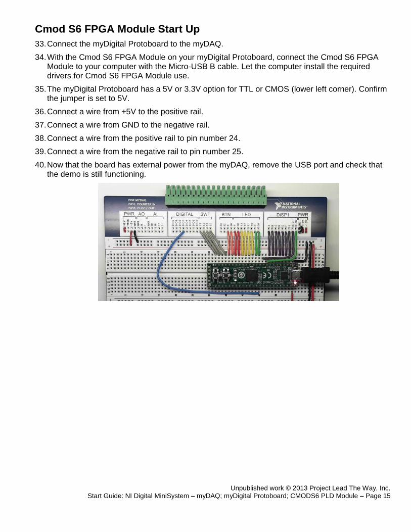
Cmod S6 FPGA Module Start Up
33. Connect the myDigital Protoboard to the myDAQ.
34. With the Cmod S6 FPGA Module on your myDigital Protoboard, connect the Cmod S6 FPGA Module to your computer with the Micro-USB B cable. Let the computer install the required drivers for Cmod S6 FPGA Module use.
35. The myDigital Protoboard has a 5V or 3.3V option for TTL or CMOS (lower left corner). Confirm the jumper is set to 5V.
36. Connect a wire from +5V to the positive rail.
37. Connect a wire from GND to the negative rail.
38. Connect a wire from the positive rail to pin number 24.
39. Connect a wire from the negative rail to pin number 25.
40. Now that the board has external power from the myDAQ, remove the USB port and check that the demo is still functioning.

Unpublished work © 2013 Project Lead The Way, Inc. Start Guide: NI Digital MiniSystem – myDAQ; myDigital Protoboard; CMODS6 PLD Module – Page 16
Cmod S6 FPGA Module Factory Loaded User Demo
The Quad SPI Flash is loaded with a configuration file at the factory. When powered on, the file will configure the FPGA such that the buttons control the states of two LEDs, while the other two LEDs toggle at a speed of about 1 Hz. The general purpose I/O pins are initially configured as inputs, and are pulled up internally by the FPGA to read a logic level ‘1’.
Cmod S6 FPGA Module Clocks
There are two clocks available on the CMODS6. There is an 8 MHz clock, and there is a 1 Hz clock. PIO14 is designated as a CLK input. See the Cmod S6 Reference Manual for more details.
Cmod S6 FPGA Module Test Files
The following three PLD Mode test files can be downloaded and unzipped to test the Cmod S6 FPGA Module. While logged into the VA, you can download the zip file here.
Internal Clock Test (DMS_14.4).ms12 – Demos how to integrate the internal clock signal of the PLD Module (Cmod S6). This test displays a 4 bit up count.
External Clock Test (DMS_14.4).ms12 – Demos how to use an external clock signal (myDAQ: Digital Writer Out). This test displays a 4 bit up count.
Multiplexed Display Test (DMS_14.4).ms12 – Demos full functionality of the Digital MiniSystem (DMS) based on the test set up configuration. This test displays a sixty second timer.
Export to PLD: Transferring a File to the Cmod S6 FPGA Module
41. Download and open “Internal Clock Test” in Multisim.
42. Connect the Cmod S6 FPGA Module to your computer if with the USB cable if not already connected.
43. Once the selected test file is open:
44. Select: Options -> Global preferences -> Paths -> Miscellaneous -> Xilinx tool path. Make sure the Xilinx tool path is set to C:\NIFPGA\programs\Xilinx14_4\ISE
45. Select: Transfer -> Export to PLD. This will bring up a menu.

Unpublished work © 2013 Project Lead The Way, Inc. Start Guide: NI Digital MiniSystem – myDAQ; myDigital Protoboard; CMODS6 PLD Module – Page 17
46. Xilinx tool:
Under the Xilinx tool drop down menu select:
“Xilinx ISE Design Suite 14.4 32-Bit or Xilinx ISE Design Suite 14.4 64-Bit”
Disregard (Unsupported) message.
Figure A Figure B
47. Programming file: Select Browse: Set your location for the programming file if you are not already there.
48. PLD part number: The PLD part number will auto-populate.
49. Advance settings: Under the advanced settings click the button on the right side of the Xilinx user constraint files row and select “Digilent C-mod S6.ufc” from pldconfig folder. See Figure B above.
Xilinx user constraint files (*.ufc): Set path to C:\Program Files\National Instruments\Circuit Design Suite 12.0\pldconfig
50. Allow unmatched LOC constraints: Yes.
51. Select: Finish
52. Exporting to the PLD will take several minutes. If the device is not found:
a. check that the USB cable is connected.
b. check user constraint path under PLD export Step 2.
c. check the Xilinx tool path under Global Settings.
d. check your Device Manager to see if “Digilent USB Device” is found.
55. “Internal Clock Test (DMS_14.4)” program should be loaded on the Cmod S6 FPGA.

Unpublished work © 2013 Project Lead The Way, Inc. Start Guide: NI Digital MiniSystem – myDAQ; myDigital Protoboard; CMODS6 PLD Module – Page 18
Checking the Test File: Internal Clock Test (DMS_14.4)
This demo will display a 4-bit binary up count on LEDs of the Cmod S6 FPGA Module, and a numerical count on the seven-segment display.
The myDigital Protoboard should be powered by the myDAQ. Wire DIG0 to GND for this demo.
Note: The seven-segment display will show the SSD equivalent of the numbers 10-15.
Circuit Design in Multisim PLD Mode
Wiring for myDigital Protoboard and the Cmod S6 FPGA

Unpublished work © 2013 Project Lead The Way, Inc. Start Guide: NI Digital MiniSystem – myDAQ; myDigital Protoboard; CMODS6 PLD Module – Page 19
Using a myDAQ Clock Signal: External Clock Test (DMS_14.4)
This demo will display a 4-bit binary up count on LEDs of the Cmod S6 FPGA Module, and a numerical count on the seven-segment display. The clock signal will be generated using the NI Elvis Digital Writer on the myDAQ.
The myDigital Protoboard should be powered by the myDAQ. Wire DIG0 to GND for this demo as it was in the first demo.
Circuit Design in Multisim PLD Mode
56. From the downloaded and unzipped folder”
Open: “External Clock Test (DMS_14.4)”
57. Export to PLD: Transfer the file to the Cmod S6 FPGA as you did with the previous test file.
58. DIO3 from the myDigital Protoboard should be wired to PIO14 of the Cmod S6 FPGA.
59. Navigate to:
Program -> National Instruments -> NI ELVISmx for NI myDAQ -> NI ELVISmx Instrument Launcher
60. Open the NI Elvis Digital Writer on the myDAQ to generate a clock signal. Select: (Write lines 0-3 Ramp 0-15)
61. To adjust the frequency of the clock, move the wire from DIO3 to DIO2 and so on to speed up the clock signal.

Unpublished work © 2013 Project Lead The Way, Inc. Start Guide: NI Digital MiniSystem – myDAQ; myDigital Protoboard; CMODS6 PLD Module – Page 20
Using the Multiplexed Display: Sixty Second Timer (DMS_14.4)
This demo will display a count from 0-60 on the multiplexed seven-segment displays. The internal clock of the Cmod S6 multiplexes the SSD so that 2 digits can be shown.
The switches (S0-S3) and buttons(B3 and B4) can be tested with outputs to RED, GREEN, and YELLOW LEDs. The myDigital Protoboard should be powered by the myDAQ.
Note: If using a student version of Multisim, you may get an error message related to the number of components in the file.
Circuit Design in Multisim PLD Mode
Wiring for myDigital Protoboard and the Cmod S6 FPGA
62. From the downloaded and unzipped folder”

Unpublished work © 2013 Project Lead The Way, Inc. Start Guide: NI Digital MiniSystem – myDAQ; myDigital Protoboard; CMODS6 PLD Module – Page 21
Open: “Sixty Second Timer (DMS_14.4)”
63. Export to PLD: Transfer the file to the Cmod S6 FPGA as you did with the previous test file.
64. DIO3 from the myDigital Protoboard should be wired to PIO14 of the Cmod S6 FPGA.
65. Navigate to:
Program -> National Instruments -> NI ELVISmx for NI myDAQ -> NI ELVISmx Instrument Launcher
66. Open the NI Elvis Digital Writer on the myDAQ to generate a clock signal. Select: (Write lines 0-3 Ramp 0-15)
67. To adjust the frequency of the clock, move the wire from DIO3 to DIO2 and so on to speed up the clock signal.
Unpublished work © 2013 Project Lead The Way, Inc. Start Guide: NI Digital MiniSystem – myDAQ; myDigital Protoboard; CMODS6 PLD Module – Page 22
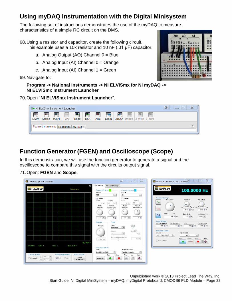
Using myDAQ Instrumentation with the Digital Minisystem
The following set of instructions demonstrates the use of the myDAQ to measure characteristics of a simple RC circuit on the DMS.
68. Using a resistor and capacitor, create the following circuit. This example uses a 10k resistor and 10 nF (.01 μF) capacitor.
a. Analog Output (AO) Channel 0 = Blue
b. Analog Input (AI) Channel 0 = Orange
c. Analog Input (AI) Channel 1 = Green
69. Navigate to:
Program -> National Instruments -> NI ELVISmx for NI myDAQ -> NI ELVISmx Instrument Launcher
70. Open “NI ELVISmx Instrument Launcher”.
Function Generator (FGEN) and Oscilloscope (Scope)
In this demonstration, we will use the function generator to generate a signal and the oscilloscope to compare this signal with the circuits output signal.
71. Open: FGEN and Scope.

Unpublished work © 2013 Project Lead The Way, Inc. Start Guide: NI Digital MiniSystem – myDAQ; myDigital Protoboard; CMODS6 PLD Module – Page 23
72. Function Generator (FGEN) Settings:
a. Waveform Settings: Square
b. Select: Run
73. Oscilloscope (Scope) Settings:
a. Channel 0 Settings:
i. Source: AI 0 (This is the CLK signal from FGEN) Check: Enabled
ii. Scale Volts/Div: 200 mV
b. Channel 1 Settings:
i. Source: AI 1 (This is the output of the circuit) Check: Enabled
ii. Scale Volts/Div: 200 mV
c. Timebase: Time/Div: 2 ms
d. Instrument Control:
i. Acquisition Mode: Run Once
The green trace is the waveform coming from the function generator. The blue trace is the output from the RC circuit. If you are using a resistor of capacitor with a different value you will need to adjust the Timebase and Volt/Div Scale so that the trace fits in the display.

Unpublished work © 2013 Project Lead The Way, Inc. Start Guide: NI Digital MiniSystem – myDAQ; myDigital Protoboard; CMODS6 PLD Module – Page 24
Digital Multimeter (DMM)
The Digital Multimeter (DMM) allows students to measure Current, Voltage, and Resistance.
In this demonstration, we will use the DMM to measure output voltage provided by the myDAQ to the myDigital Protoboard. The DMM is fused for protection when reading current.
74. Open: DMM
75. DMM Settings:
a. Measurement Settings:
i. DC Voltage
ii. Range 60V
76. Make sure the Banana Jack Connection match the diagram and they touching the +5V and GND on the DMS as pictured.
77. Select : Run
78. Change the Range to 20V and note the difference.
79. Change the Range to 2V and note the difference. Switch back to 20V range.

Unpublished work © 2013 Project Lead The Way, Inc. Start Guide: NI Digital MiniSystem – myDAQ; myDigital Protoboard; CMODS6 PLD Module – Page 25
Optional Support: Digital Logic Board (DLB)
NI DEFB Driver Installation for use with the Digital Logic Board (DLB)
The following instructions describe the installation process on the NI DEFB Driver for use on the Digital Logic Board in your classroom. If using the DMS and DLB, each board requires a different driver.
1. Download and install: DEFB Driver (32 and 64 bit). The DEFB Driver can be located on the Virtual Academy Here:
Technical Support & Software Downloads--> Pathway To Engineering ->DE->Optional->FPGA Drivers 32/64
2. Once downloaded, extract the driver files and run setup.exe. Follow the prompts to install and upon completion, reboot the machine.
3. Plug the DLB into a USB port on your computer and power it on. With your speakers turned on, you will hear the USB port chime on and off a few times.
a. For 32-bit XP users, the driver wizard will pop up three times. The path to the driver is: C:\Program Files\National Instruments\FPGA.
Digital Logic Board (DLB): Transfer → Export to PLD Process
4. Download and open “External Clock Test (DLB_12.4)” in Multisim.
5. Connect the DLB to your computer with the USB cable if not already connected.
6. Once the selected test file is open:
Select: Options -> Global preferences -> Paths -> Miscellaneous -> Xilinx tool path. Make sure the Xilinx tool path is set to C:\NIFPGA\programs\Xilinx12_4\ISE.

Unpublished work © 2013 Project Lead The Way, Inc. Start Guide: NI Digital MiniSystem – myDAQ; myDigital Protoboard; CMODS6 PLD Module – Page 26
7. Select: Transfer -> Export to PLD. This will bring up a menu. Select: Next
8. Xilinx tool:
Under the Xilinx tool drop down menu select:
Xilinx ISE Design Suite 12.4 32-Bit or Xilinx ISE Design Suite 12.4 64-Bit
Figure A Figure B
1. Programming file: Select Browse: Set your location for the programming file if you are not already there.
2. PLD part number: The PLD part number will auto-populate.
Advance settings: Under the advanced settings click the button on the right side of the Xilinx user constraint files row. Navigate to and select “DEFB.ufc” from pldconfig folder.
Xilinx user constraint files (*.ufc): Set path to C:\Program Files\National Instruments\Circuit Design Suite 12.0\pldconfig

Unpublished work © 2013 Project Lead The Way, Inc. Start Guide: NI Digital MiniSystem – myDAQ; myDigital Protoboard; Cmod S6 FPGA Module – Page 27
3. Allow unmatched LOC constraints needs be set to yes.
4. Click finish.
5. Exporting to the PLD will take several minutes. If the device is not found:
check that the USB cable is connected.
check user constraint path under PLD export Step 2.
check the Xilinx tool path under Global Settings.
check your Device Manager to see if “Digilent USB Device” is found.
6. With RotCLK wired to GPIO0 you should be a a count of 0-60 on the Seven Segment Displays. You can change the rate using ROT1
RotCLK GPIO0
ROT1