compensation of reactive power and sag voltage using
TRANSCRIPT

12
Compensation of Reactive Power and Sag Voltage Using Superconducting Magnetic
Energy Storage System
Mohammad Reza Alizadeh Pahlavani Malek-Ashtar University of Technology (MUT), Shabanlo St., Lavizan, Tehran
Iran
1. Introduction
Technological developments such as Flexible AC Transmission Systems (FACTS) can improve the power quality of the power system and can respond to the ever-increasing demand for electrical energy. Superconducting magnetic energy storage (SMES) is a FACTS device that has been used for several years at utility and industrial sites throughout the United States, Japan, Europe, and South Africa to provide both transmission voltage support and power quality to customers who are vulnerable to fluctuating power quality [1]-[3]. SMES systems are classified into two groups: voltage source inverter (VSI) and current source inverter (CSI) SMES. The VSI SMES has many advantages when compared with the CSI SMES; for example, in the VSI SMES, the power rating of power electronic devices that are used in the inverter is much less than that of the CSI SMES, resulting in fewer switching and power losses. Also, the VSI SMES can be used as a Static synchronous Compensator (STATCOM) when its chopper is out of service. Moreover, for the same condition, the VSI SMES can store more energy than the CSI SMES; these advantages encouraged the authors to study VSI SMES. This type of SMES is composed of a magnetic energy storage coil with various structures and power conditioning systems that are also composed of different parts, such as AC-DC filters, a multi-level chopper, a capacitor bank, and a multi-level converter (i.e. an inverter or rectifier). These power conditioning systems are also used in many different sustainable energy systems, such as bio fuels, solar power, wind power, wave power, geothermal power, and tidal power. The converter is an interface between the power network and the capacitor bank and controls the electrical energy exchange between the two. Likewise, the chopper is also an interface between the magnetic energy storage coil and the capacitor bank, and controls electrical energy exchange between them. To store the electrical energy in the capacitor bank and the magnetic energy storage coil in the range of mega joules, it is necessary to employ high power-rating converters; to overcome the limitations of the current and voltage range of the semiconductors, multi-level converters are used. The advantages of using such converters include reducing voltage on the switches, harmonic order correction, decreasing or eliminating lateral equipment, decreasing switching frequency, decreasing total harmonic distortion (THD), decreasing switching losses, and decreasing the output current ripple.

Power Quality – Monitoring, Analysis and Enhancement
256
Multi-level converters, on the other hand, have some disadvantages associated with their use, such as the complexity of the control systems, increasing the number of power electronic devices, and increasing the asymmetry of the capacitor voltages during charge and discharge [4]-[8]. However, the trend toward increasing the speed of electronic processors and the steady decrease in the cost of power electronic devices, coupled with the ability to implement advanced modulation methods such as the SVPWM, encourage engineers to ignore the disadvantages of multi-level converters. There are three different multi-level voltage source converters: diode-clamped, flying capacitor, and cascade H-bridge. For the same voltage level, there are fewer capacitors in a diode-clamped multi-level converter than in the other multi-level converters, making it much more cost-effective than other two converters. When there are three voltage levels, a three-level diode-clamped converter is referred to as a neutral point clamped (NPC). With respect to the fact that an appropriate choice of switching strategy for SVPWM effectively reduces the low order harmonics, a novel and optimized switching strategy for SVPWM has been proposed for the first work in this chapter in order to mitigate some low order harmonics in the NPC voltage source inverter [9]-[13]. Depending on its application, a SMES device is controlled in two ways: first, the transmitted active and reactive power to the network is controlled using a NPC voltage source inverter and the capacitor voltage is stabilized using a chopper. In the second approach, the NPC voltage source inverter controls the transmitted reactive power to the network while stabilizing the capacitors voltage and the chopper controls the transmitted active power to the network. It should be noted that if the capacitors voltage is stabilized during all switching operations, low-capacity capacitors can be used in the SMES system, resulting in a lower cost of configuration. The voltage variation in low-capacity capacitors is faster during the course of supplying the power network by the SMES; consequently, a controller with a differential part, i.e. PID, will make the capacitor’s voltage unstable and will transmit any noise to the power electronic devices of the chopper. Thus, PI controllers are used in this study to stabilize the capacitors voltage of the SMES by generating the real-time duty cycles of the three-level chopper in different operation modes. Stabilization of capacitors voltage will correct any imbalance due to asymmetry within the SMES circuit and its operation.
Fig. 1. The VSI SMES

Compensation of Reactive Power and Sag Voltage Using Superconducting Magnetic Energy Storage System
257
Power quality is involved with a wide range of electromagnetic phenomena such as transient state, short- and long-term variations, voltage imbalance and variations, wave distortion, and frequency oscillations in power systems. In fact, the magnitude of variations in voltage, current, and frequency within power systems determines the power quality. In recent years, the voltage quality has been hailed as the most important index of power quality. Among voltage quality indicators, voltage sag has been shown to be especially important; voltage sag is defined as a temporary voltage drop that lasts between 0.5 and 30 cycles, and has a typical magnitude of 0.1 to 0.9 per unit range [14], [15]. A voltage sag can cause the same amount of downtime as a complete loss of power, especially if, for example, machines need to be rebooted or production processes need to be restarted. This issue poses a major challenge when estimating the economic cost of power interruptions and power-quality events. One way to compensate for voltage sag is to use VSI SMES, which is studied as a second work in this chapter by proposing a novel compensation algorithm. So this chapter presents a novel and optimized switching strategy and control approach for a three-level two-quadrant chopper in a three-level Neutral point clamped (NPC) voltage source inverter (VSI) superconducting magnetic energy storage (SMES). Using the proposed switching strategy, the voltage of the inverter capacitors in SMES can be independently controlled; also, the minimum power and switching losses - as well as the proper convection - can be achieved using this same strategy. The simulation results indicate that when combined with a proportional-integral (PI) control approach the proposed switching strategy can be easily implemented in the power networks and can balance and stabilize the multi-level inverters’ capacitor voltage level. The voltage variation of the capacitors in the steady state condition is less than (0.062%) which is 15 times better than the IEEE standard requirement (1%). To investigate the effectiveness and reliability of the proposed approach in stabilizing capacitor voltage, SMES performance using the presented approach is compared with that of SMES when the capacitors of the three-level inverter are replaced with equal and ideal voltage sources. This comparison is carried out from the power quality point of view and it is shown that the proposed switching strategy with a PI controller is highly reliable [16]- [17]. Considering that the Space Vector Pulse Width Modulation (SVPWM) is highly effective in decreasing low order harmonics, this article utilizes this type of modulation when it is combined with the most optimized switching strategy. In addition, this chapter proposes a new algorithm for SMES to compensate the voltage sag in the power networks. Simulation results show that the VSI SMES, when combined with the proposed algorithm, is able to compensate the voltage sag and phase voltage in less than one cycle, which is 5 times better than other voltage sag compensators.
2. Switching strategies of the three-level NPC inverter
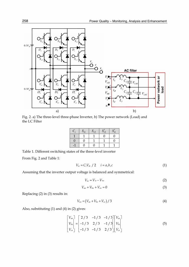
Fig. 2 shows a case study in which a three-level NPC inverter supplies the three phase power network. A filter is used between the inverter and the power network to eliminate the high order harmonics; it is noted that parts of the low order harmonics are mitigated by applying SVPWM. Different switching states of the three-level NPC inverter are shown in Table 1: 1 and 0 indicate the on/off states of the switches, respectively. As seen in this table, in order to prevent a capacitor leg short-circuit, all switches in a leg are never turned on simultaneously.
Power Quality – Monitoring, Analysis and Enhancement
258
a) b)
Fig. 2. a) The three-level three-phase Inverter, b) The power network (Load) and the LC Filter
1iS ′ 2iS ′
2iS 1iS iC
0 0 1 1 1
0 1 1 0 0
1 1 0 0 -1
Table 1. Different switching states of the three-level inverter
From Fig. 2 and Table 1:
/ 2 , ,= =io i dcV C V i a b c (1)
Assuming that the inverter output voltage is balanced and symmetrical:
= −io noinV V V (2)
0+ + =an bn cnV V V (3)
Replacing (2) in (3) results in:
( ) /3= + +no ao bo coV V V V (4)
Also, substituting (1) and (4) in (2) gives:
2 / 3 1 / 3 1 / 3
1 / 3 2 / 3 1 / 3
1 / 3 1 / 3 2 / 3
− − = − −
− −
an ao
bn bo
cn co
V V
V V
V V
(5)
Compensation of Reactive Power and Sag Voltage Using Superconducting Magnetic Energy Storage System
259
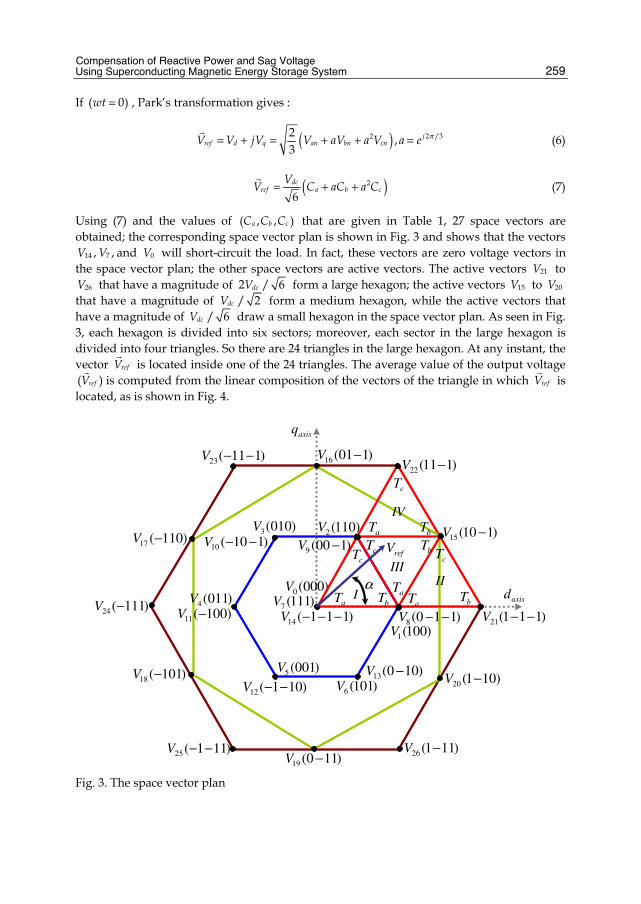
If ( 0)=wt , Park’s transformation gives :
( ) 2 /322,
3= + = + + =
j
ref d q an bn cnV V jV V aV a V a e π (6)
( )2
6= + +
dc
ref a b cV
V C aC a C (7)
Using (7) and the values of ( , , )a b cC C C that are given in Table 1, 27 space vectors are
obtained; the corresponding space vector plan is shown in Fig. 3 and shows that the vectors
14 7, ,V V and 0V will short-circuit the load. In fact, these vectors are zero voltage vectors in
the space vector plan; the other space vectors are active vectors. The active vectors 21V to
26V that have a magnitude of 2 / 6dcV form a large hexagon; the active vectors 15V to 20V
that have a magnitude of / 2dcV form a medium hexagon, while the active vectors that
have a magnitude of / 6dcV draw a small hexagon in the space vector plan. As seen in Fig.
3, each hexagon is divided into six sectors; moreover, each sector in the large hexagon is
divided into four triangles. So there are 24 triangles in the large hexagon. At any instant, the
vector
refV is located inside one of the 24 triangles. The average value of the output voltage
( )
refV is computed from the linear composition of the vectors of the triangle in which
refV is
located, as is shown in Fig. 4.
)110(2V
)000(0Vaxisd
)111(7V)111(14 −−−V
)010(3V
)101(6V)101(12 −−V
)011(4V
)101(20 −V
)110(17 −V )110(15 −V
)111(21 −−V)111(24 −V
)101(18 −V
)111(25 −−V )111(26 −V)110(19 −V
)111(23 −−V )101(16 −V)111(22 −V
)100(1V)110(8 −−V
)100(9 −V)110(10 −−V
)100(11 −V
)001(5V )100(13 −V
axisq
aTbT
cT
aT bT
cT
aT bT
cT
aT
bTcT refV
αI
IV
IIIII
Fig. 3. The space vector plan
Power Quality – Monitoring, Analysis and Enhancement
260
0V
axisd7V
14V
axisqaT
bTcT refV
aαbα
α
cα
aV
bV
cV
Fig. 4. Operation time calculation of each triangle vector
0 0
+
+
= + + S a a b S
a a b
T T T T T
ref a b c
T T T
V dt V dt V dt V dt (8)
= + +
S ref a a b b c cT V T V T V T V (9)
The projection of the vectors in (9) on the d-q axis and composing the obtained vectors results in:
cos cos cos cos= + +
s ref a a a b b b c c cT V T V T V T Vα α α α (10)
sin sin sin sin= + +
s ref a a a b b b c c cT V T V T V T Vα α α α (11)
2,
6
,
2
=
+ + =
+ = =
a ref dc
a b c S
inv
m V V
T T T T
t ftω ϕ π α
(12)
where am is the modulation index, ST is the switching period [the inverse of the switching
frequency ( )Sf ], invϕ is the inverter phase, and f is the frequency of the inverter output
voltage. Assuming that the switching period, the phase, and the magnitude of the vectors
, , ,
ref a bV V V and
cV are known, solving equations (10), (11), and (12) gives , ,a bT T and
cT . These, shown in each triangle in Fig. 3, determine the operation time of the triangle
vectors. Note that by knowing the value of + invtω ϕ at any time, the number of the space
sector in which
refV is located can be determined. The above equations can be extended to all
sectors of the large hexagon by changing α to (( 1) / 3)− −nα π where 1 , ... , 6=n is the
sector number. Table 2 gives the operation times of the vectors of the 4 triangles created in
the thn sector.

Compensation of Reactive Power and Sag Voltage Using Superconducting Magnetic Energy Storage System
261
, ,=iT i a b c triangles’ number
= − −a s b cT T T T
2 2 sin( / 3) /= − +b ref S dcT V T n Vα π
2 2 sin( ( 1) / 3) /= − −c ref S dcT V T n Vα π
I
= − −a s b cT T T T
2 2 sin( / 3) /= − +b ref S dcT V T n Vα π
2 2 sin /=c ref S dcT V T Vα
II
= − −a s b cT T T T
2 2 cos( (1 2 ) /6) /= − + + −b s ref S dcT T V T n Vα π
2 2 sin( / 3) /= − − +c s ref S dcT T V T n Vα π
III
= − −a s b cT T T T
2 2 sin( / 3) /= − +b ref S dcT V T n Vα π
2 2 sin( ( 1) / 3) /= − + − −c s ref S dcT T V T n Vα π
IV
Table 2. The operation times of the vectors of 4 triangles of the nth sector
Depending on the number of space vectors in each sector and the operation time of each
space vector in generating ,
refV many different switching strategies can be presented. The
authors of the present work demonstrated that, in order to minimize THD in the inverter
output voltage, the zero vectors should be distributed at the beginning, middle, and end of
the switching periods in each sector whenever possible, [23]-[24]. Also, to minimize the
switching losses, this distribution should be performed so that the minimum number of
displacements in the switching states in each switching period of each sector occurs. The
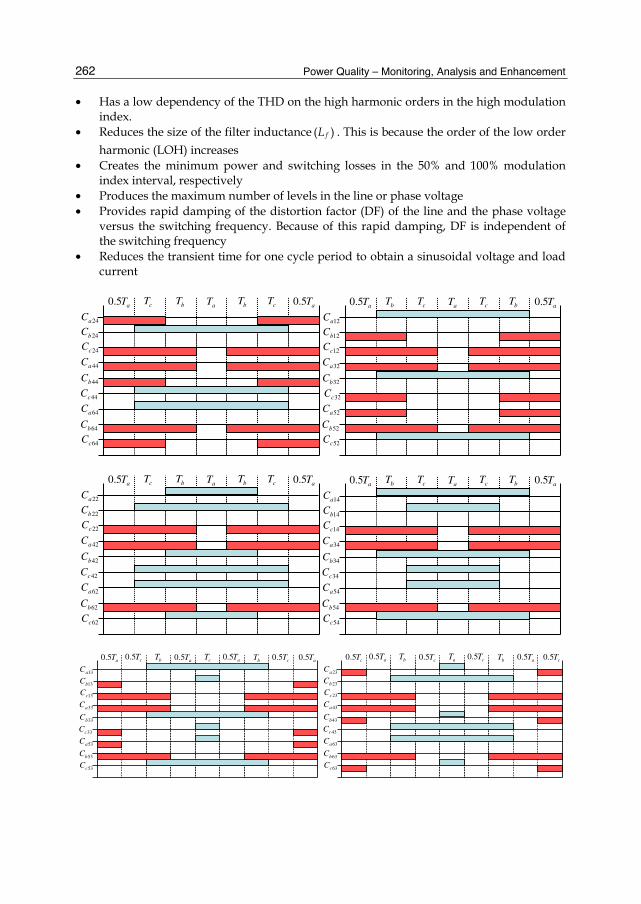
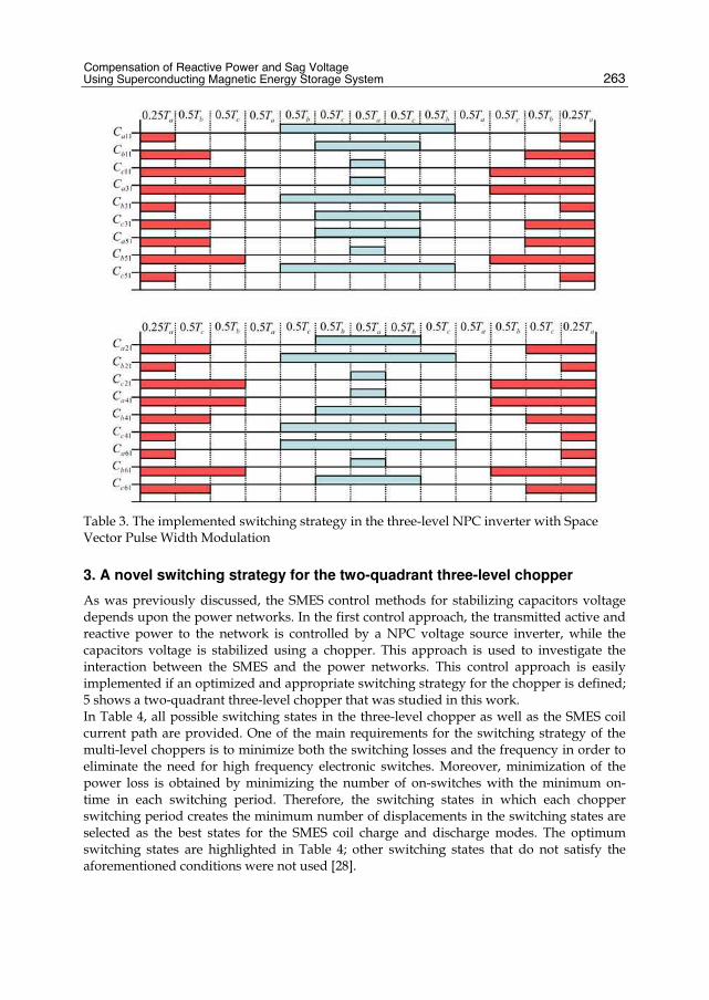
switching strategy of the space vector pulse width modulation is shown in Table 3; this
strategy is based on the 24 triangles that were generated in the large hexagon as previously
indicated. This switching strategy is implemented such that both the minimum THD and
the minimum switching losses are realized. Note that aijC in this table indicates the
switching states in the inverter leg-a at sector i in triangle j. It should also be noted that the
operation time of the vectors of each triangle in this switching strategy is determined by the
times indicated in each triangle shown in Fig. 3. The switching strategy shown in Table 3 is
the most appropriate strategy among the other switching strategies of the SVPWM [23]
because it:
• Minimizes the THD in the line voltage
• Has the minimum THD in the phase voltage in 60% of the modulation index interval
• Creates the minimum number of the harmonic orders in both the line and the phase voltage, resulting in the minimum distortion power losses
• Has the minimum ratio of harmonic orders to the fundamental order
• Has the minimum switching losses to switching frequency ratio
Power Quality – Monitoring, Analysis and Enhancement
262
• Has a low dependency of the THD on the high harmonic orders in the high modulation index.
• Reduces the size of the filter inductance ( )fL . This is because the order of the low order
harmonic (LOH) increases
• Creates the minimum power and switching losses in the 50% and 100% modulation index interval, respectively
• Produces the maximum number of levels in the line or phase voltage
• Provides rapid damping of the distortion factor (DF) of the line and the phase voltage versus the switching frequency. Because of this rapid damping, DF is independent of the switching frequency
• Reduces the transient time for one cycle period to obtain a sinusoidal voltage and load current
aT5.0
64cC
44cC
cT bT
64bC
64aC
44bC
44aC
24cC24bC
24aC
aT bT cT aT5.0aT5.0
52cC
32cC
bT cT
52bC
52aC
32bC
32aC
12cC
12bC
12aC
aT cT bT aT5.0
aT5.0
62cC
42cC
cT bT
62bC
62aC
42bC
42aC
22cC
22bC
22aC
aT bT cT aT5.0aT5.0
54cC
34cC
bT cT
54bC
54aC
34bC
34aC
14cC14bC
14aC
aT cT bT aT5.0
aT5.0
53cC
33cC
cT5.0 bT
53bC
53aC
33bC
33aC
13cC
13bC
13aC
aT5.0 cT aT5.0bT cT5.0 aT5.0
cT5.0
63cC
43cC
aT5.0 bT
63bC
63aC
43bC
43aC
23cC
23bC
23aC
cT5.0 aT cT5.0bT aT5.0 cT5.0
Compensation of Reactive Power and Sag Voltage Using Superconducting Magnetic Energy Storage System
263
Table 3. The implemented switching strategy in the three-level NPC inverter with Space Vector Pulse Width Modulation
3. A novel switching strategy for the two-quadrant three-level chopper
As was previously discussed, the SMES control methods for stabilizing capacitors voltage depends upon the power networks. In the first control approach, the transmitted active and reactive power to the network is controlled by a NPC voltage source inverter, while the capacitors voltage is stabilized using a chopper. This approach is used to investigate the interaction between the SMES and the power networks. This control approach is easily implemented if an optimized and appropriate switching strategy for the chopper is defined; 5 shows a two-quadrant three-level chopper that was studied in this work. In Table 4, all possible switching states in the three-level chopper as well as the SMES coil current path are provided. One of the main requirements for the switching strategy of the multi-level choppers is to minimize both the switching losses and the frequency in order to eliminate the need for high frequency electronic switches. Moreover, minimization of the power loss is obtained by minimizing the number of on-switches with the minimum on-time in each switching period. Therefore, the switching states in which each chopper switching period creates the minimum number of displacements in the switching states are selected as the best states for the SMES coil charge and discharge modes. The optimum switching states are highlighted in Table 4; other switching states that do not satisfy the aforementioned conditions were not used [28].

Power Quality – Monitoring, Analysis and Enhancement
264
Current path 1 2 1 2( , , , )′ ′d d d dS S S S loadV Mode
1 2 1 2, , ,′ ′d d d dS S S S (1111) 1 2+C CV V FCM
1 2 2, , ,′ ′d d d dS S D S (0111) 2CV
1 2, , ,′ ′d d d dS D D S (0110) 0
1 1 2, , ,′ ′d d d dS D S S (1110) 1CV
CM
, ′e eD D (0000) 1 2− −C CV V FDM
1 , ,′ ′ ′d d eS D D (0010) 2− CV
1 2, , ,′ ′d d d dS D D S (0110) 0
2, ,e d dD D S (0100) 1− CV
DM
1 2, ,e d dD S S (1100) 0
1 2, ,e d dD S S (1101) 0
1 2, ,′ ′ ′d d eS S D (1011) 0
1 2, ,′ ′ ′d d eS S D (0011) 0
2, ,e d dD D S (0101) 1− CV
, ′e eD D (1010) 1 2− −C CV V
, ′e eD D (1001) 1 2− −C CV V
, ′e eD D (1000) 1 2− −C CV V
, ′e eD D (0001) 1 2− −C CV V
Un
usa
ble
Table 4. Switching states in a two-quadrant three-level chopper
Another requirement in the switching strategy of the multi-level choppers is the
independent action of the capacitors voltage controllers. The switching strategy that satisfies the two cited requirements is outlined in Table 5. The charge and discharge modes (CM and DM) in Table 5 are obtained from the proper states in Table 4, assuming that the chopper
switching period is 2 chT .
Note that oT and uT are, respectively, the operation times that the voltage of the upper and
lower capacitors are connected to the positive and the negative polarities of the load during
the charge and the discharge modes. Also, zT is the chopper operation time when the load is
short circuit; this occurs at both the charge and discharge modes. Hence, the duty cycles of
the chopper can be defined as follows:
2 , 2 , 2= = + + =o o ch u u ch o u z chd T T d T T T T T T (13)
From this equation, it can be seen that , ,o ud d and zd vary within the range [0, 1]. Also,
Table 5 shows that in the charge and the discharge modes, +o ud d is always less than one,
which means that the required time for compensating the capacitor voltage to the reference
voltage is less than a single switching period of the chopper. In other words, if +o ud d is
more than one, the required time for the compensation of the capacitors voltage to the
reference voltage will be more than a single switching period of the chopper. In this case, the compensation of the capacitors voltage to the reference voltage should be performed simultaneously. The fast charge and discharge (FCM and FDM) modes have

Compensation of Reactive Power and Sag Voltage Using Superconducting Magnetic Energy Storage System
265
been considered for this case; note that in changing from the fast charge mode to the charge mode, or from the fast discharge mode to the discharge mode and vice versa, the minimum number of switch displacements of each chopper switching period occurs, resulting in a
minimum of switching losses presenting an advantage of the proposed switching strategy.
a)
b)
Fig. 5. a) The two-quadrant three-level chopper, b) The load (DC filter and SMES coil)
Table 5. The implemented switching strategy in the two-quadrant three-level chopper

Power Quality – Monitoring, Analysis and Enhancement
266
4. Chopper duty cycle controller design
In this section, a block diagram for generating the duty cycle of CM and FCM is presented (Fig. 6). To enhance the system dynamic response when balancing the capacitors voltage, it is necessary to ensure that the capacitors voltages are equal prior to connecting the inverter to the power network. To achieve this, the voltages of the upper and the lower capacitors are
compared with the reference voltage, which is assumed to be 0.5 dcV , as seen in Fig. 6.
Subsequently, the difference in the voltages is passed through the limiters with [0 0.5] interval. These limiters work so that each capacitor is charged for only 50% of the switching period; in fact, the outputs of these limiters can only produce the charge mode (CM). After connecting the inverter to the power network, the PI controllers begin operating and the voltage errors are fed to these controllers. Using the signal holders, the outputs of the PI
controllers are sampled every 2 chT period. The signal holders with a 2 chT sampling time are
used to avoid abrupt variations in the duty cycles. If the duty cycles vary abruptly, the turn on/off times should be zero, but this is practically impossible. The signal holder outputs are passed through the limiters with [0 1] interval; these limiters can produce both the charge and the fast charge modes (CM, FCM).
a) b)
Fig. 6. The chopper duty cycle controller
With the availability of , ,o ud d chT , and by using the Embedded MATLAB Functions shown
in Fig. 6, the various modes of the chopper (CM, FCM, DM, and FDM) can be determined.
Finally using these modes, the corresponding switching strategies are applied to the
chopper switches based on Table 5.
5. Simulation results of the switching strategy of the three-level chopper
In this section, the strategies presented in sections 2 through 4 are simulated using MATLAB® software. The power network to which the SMES is connected is shown in Fig. 7 and was modeled using the M-file in MATLAB®. The power network and the SMES parameters are given in Appendix I. In Fig. 8, the SMES performance using the developed approaches is compared with that of the SMES when the capacitors of the three-level NPC inverter are replaced with equal and ideal voltage sources (SMES with ideal VSI). These comparisons are from the perspective of the THD and the DF of the inverter output line voltage. As seen in this figure, the

Compensation of Reactive Power and Sag Voltage Using Superconducting Magnetic Energy Storage System
267
performance of the SMES using the chopper duty cycle controller is the same as that of the SMES with an ideal VSI.
Fig. 7. The power network
Fig. 8. THD and DF variation of the inverter output line voltage

Power Quality – Monitoring, Analysis and Enhancement
268
Fig. 9 shows the voltage variation of the capacitors versus the modulation index; this figure indicates that the proposed schemes are capable of stabilizing the capacitors voltage to the reference voltage (with less than 0.5% error in the worst case scenario). The smallest voltage variation (with 0.0625% error) is obtained when the modulation index is 0.65, as shown in Figure 9. This is because PI controllers have been regulated for this modulation index; in short, the variation of the capacitor voltage depends on both the modulation index and the parameters of the PI controllers. Therefore, in order to obtain the best results, it is recommended that the parameters of the PI controllers be deregulated for each modulation index.
Fig. 9. The capacitors voltage variation versus index modulation
Fig. 10. The current and the voltage of the SMES coil and the current of the load

Compensation of Reactive Power and Sag Voltage Using Superconducting Magnetic Energy Storage System
269
Fig. 10 shows the voltage and current of the SMES coil and the current of the load. From this figure, it can be seen that the current of the SMES coil is decreasing, or rather, that the stored energy in the coil is discharging. The discharged energy is transmitted to the chopper in the active power form because in this transmission, the current of the load and the voltage of the SMES coil remain constant.
a)
b)
Fig. 11. a) The voltage of the capacitor fdcC and the chopper duty cycle percent,
b) Steady state duty cycle percent
Fig. 11 depicts the variation of the chopper duty cycle and the voltage of the DC filter
capacitor. In this figure, the inverter is connected to the power network at 0.08 [sec]=t . It is
concluded from this figure that before 0.08 [sec]=t , the CM mode has been selected by the

Power Quality – Monitoring, Analysis and Enhancement
270
Embedded MATLAB function, and after this time, both the CM and the FCM modes have
been selected as well. Also, as observed in Fig. 11a, the voltage of the fdcC is important in
stabilizing the voltage of the SMES coil; Fig. 11b shows that in steady state condition, only
the CM mode occurs for this power network.
Fig. 12 shows the voltage variation of the capacitors; the initial voltages of the capacitors 1C
and 2C were 9800 [ ]V and 9500 [ ]V , respectively. As noticed in Fig. 12, the proposed
switching strategy properly stabilizes the capacitors voltage before and after connecting the
inverter to the power net-work. In Fig. 12, the voltage variations of the capacitors in the
steady state condition, as can be verified in Fig. 9, is less than 6.25 [ ]V (0.062%) Compared
with the values defined in the IEEE standard specifications and obtained in [27] (i.e. 1% ),
this value has been reduced approximately 15 times.
Fig. 12. Variation of the voltage of the capacitors 1C and 2C
The parameters of the PI controllers, as seen in Appendix I, should be independently tuned
for the upper and lower capacitors. This is because when using the SVPWM, the upper and
the lower capacitors are not discharged at the same rate; consequently, the number of the PI
controllers should be equal to that of the level of the inverters, and the parameters of each PI
controller should be independently tuned. In fact, using this approach, the voltage of the
inverter capacitors can be stabilized even when the power network is asymmetric and
unbalanced. To verify the simulation results obtained by the proposed switching strategy
given in Tables 3 and 4, part of the implemented switching strategy in the inverter and the
three-level chopper are shown in Figs. 13 and 14, respectively. These figures show that the
carrier waves of the chopper and the inverter are triangular, that the period of these carrier
waves for the inverter and the chopper are 2 0.001 [sec]=ST and 2 0.001 [sec]=chT , and that
their magnitudes are ST and chT , respectively. In Fig. 15, the steady state line voltage and the current of loads 2 and 3 are shown. Fig. 16 shows the steady state line voltage and the current of the inverter prior to filtering.

Compensation of Reactive Power and Sag Voltage Using Superconducting Magnetic Energy Storage System
271
Comparisons of Figs. 15 and 16 show that the AC passive filter successfully filters out the current and the voltage harmonics that are produced by the inverter at the load terminals.
Fig. 13. Part of the proposed switching strategy for the inverter using the SVPWM
Fig. 14. Part of the proposed switching strategy for the three-level chopper

Power Quality – Monitoring, Analysis and Enhancement
272
0.35 0.355 0.36 0.365 0.37 0.375 0.38 0.385 0.39 0.395 0.4-2
-1
0
1
2
Vlin
e [
KV
]
Modulation index = 0.65 & Number of Load = 2
0.35 0.355 0.36 0.365 0.37 0.375 0.38 0.385 0.39 0.395 0.4-2
-1
0
1
2
I line [
KA
]
Time [sec]
a)
0.35 0.355 0.36 0.365 0.37 0.375 0.38 0.385 0.39 0.395 0.4
-2
-1
0
1
2
Vlin
e [
KV
]
Modulation index = 0.65 & Number of Load = 3
0.35 0.355 0.36 0.365 0.37 0.375 0.38 0.385 0.39 0.395 0.4-3
-2
-1
0
1
2
3
I line [
KA
]
Time [sec]
b)
Fig. 15. Steady state line voltage and the current of the loads: a) No.2, b) No.3.

Compensation of Reactive Power and Sag Voltage Using Superconducting Magnetic Energy Storage System
273
0.35 0.355 0.36 0.365 0.37 0.375 0.38 0.385 0.39 0.395 0.4-30
-20
-10
0
10
20
30
Vlin
e [
KV
]
Modulation index = 0.65 & voltage and current of inverter
0.35 0.355 0.36 0.365 0.37 0.375 0.38 0.385 0.39 0.395 0.4-4
-2
0
2
4
I line [
KA
]
Time [sec]
Fig. 16. The steady state output voltage and the current of the inverter
6. Voltage sag compensation algorithm
Here, a new algorithm is presented to compensate the sag voltage in an R-L load using SMES. Fig. 17 shows the configuration of the studied power network, the R-L loads, and the SMES.
Fig. 17. Configuration of the R-L load, the SMES, and the power network
To compensate the voltage sag using SMES, it is necessary that the proper values of am and
invϕ be calculated and applied to the inverter. If the phasor voltage of the R-L load 2
Power Quality – Monitoring, Analysis and Enhancement
274
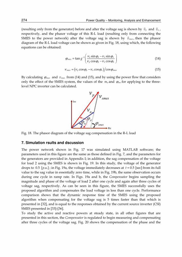
(resulting only from the generator) before and after the voltage sag is shown by
pv and
nv ,
respectively, and the phasor voltage of this R-L load (resulting only from connecting the
SMES to the power network) after the voltage sag is shown by ,
smesv then the phasor
diagram of the R-L load voltage can be shown as given in Fig. 18, using which, the following
equations can be obtained:
1 sin sintan
cos cos− −
= − p p n n
smes
p p n n
gν ϕ ν ϕ
ϕν ϕ ν ϕ
(14)
( )cos cos cos= −smes p p n n smesν ν ϕ ν ϕ ϕ (15)
By calculating smesϕ and smesv from (14) and (15), and by using the power flow that considers
only the effect of the SMES system, the values of the am and invϕ for applying to the three-
level NPC inverter can be calculated.
Fig. 18. The phasor diagram of the voltage sag compensation in the R-L load
7. Simulation rsults and dscussion
The power network shown in Fig. 17 was simulated using MATLAB software; the
parameters used in this figure are the same as those defined in Fig. 7, and the parameters for
the generators are provided in Appendix I; in addition, the sag compensation of the voltage
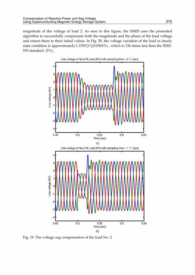
for load 2 using the SMES is shown in Fig. 19. In this study, the voltage of the generator
drops to 0.5 [ . .]p u ; in Fig. 19a, the voltage immediately decreases at 0.5=t [sec] from its full
value to the sag value in essentially zero time, while in Fig. 19b, the same observation occurs
during one cycle in ramp rate. In Figs. 19a and b, the Compensator begins sampling the
magnitude and phase of the voltage of load 2 after one cycle and again after three cycles of
voltage sag, respectively. As can be seen in this figure, the SMES successfully uses the
proposed algorithm and compensates the load voltage in less than one cycle. Performance
comparison shows that the dynamic response time of the SMES using the proposed
algorithm when compensating for the voltage sag is 5 times faster than that which is
presented in [32], and is equal to the responses obtained by the current source inverter (CSI)
SMES presented in [33]-[36].
To study the active and reactive powers at steady state, in all other figures that are
presented in this section, the Compensator is regulated to begin measuring and compensating
after three cycles of the voltage sag. Fig. 20 shows the compensation of the phase and the
Compensation of Reactive Power and Sag Voltage Using Superconducting Magnetic Energy Storage System
275
magnitude of the voltage of load 2. As seen in this figure, the SMES uses the presented
algorithm to successfully compensate both the magnitude and the phase of the load voltage
and return them to their initial values. In Fig. 20, the voltage variation of the load in steady
state condition is approximately 1.1559 [ ] (0.0365%)V , which is 136 times less than the IEEE-
519 standard (5%) .
a)
b)
Fig. 19. The voltage sag compensation of the load No. 2

Power Quality – Monitoring, Analysis and Enhancement
276
Fig. 20. Compensation of the phase and magnitude of the voltage of the load No. 2.
8. Conclusion
In this study an appropriate switching strategy for the NPC VSI with several advantages for the SMES regarding its ability to improve the performance of this device was presented. Some advantages of using this strategy for the NPC VSI presented in this chapter include:
• Optimizing power quality by implementing a proper switching strategy in SVPWM for VSI SMES
• Better stabilization of the capacitors voltage of the VSI SMES than that of the IEEE standard
• Implementing the rapid charge and discharge modes as opposed to the charge and discharge modes in order to increase the dynamic response time when stabilizing the capacitors voltage of the VSI SMES
• Independent control of the capacitors voltage in the VSI SMES for compensating asymmetric and unbalanced loads
• Minimizing the switching and power losses, resulting in easy and reliable convection from multi-level converter’s switches
• Using the proposed switching strategies, resulting in the power quality becoming equal with the case in which the capacitors of the inverter are replaced with an ideal and equivalent voltage source (SMES with ideal VSI)
• Effective and highly reliable performance of the presented strategy when used with a PI control approach
• Compensating capacitors voltage of the VSI SMES prior to connecting the SMES to the power network (stand-by mode)
• Furthermore, an algorithm was presented for the VSI SMES in order to compensate the voltage sag. Some advantages of the proposed algorithm include:
• Compensating the voltage sag and the voltage phase of the load in less than one cycle

Compensation of Reactive Power and Sag Voltage Using Superconducting Magnetic Energy Storage System
277
• Compensating the active and the reactive power in less than four cycles
• Load voltage stabilizing in good agreement with the IEEE-519 standard
9. Appendix I
The parameters of the PI controllers:
0.1, 0.1, 0.04, 0.03= = = =O O U UKP KI KP KI
Specifications of the transmission line:
1 1 2
2 3 3
15 [ ], 1.5 [ ], 15 [ ],
1.5 [ ], 30 [ ], 3 [ ]
= Ω = Ω = Ω
= Ω = Ω = Ω
L L L
L L L
X R X
R X R
Specifications of the synchronous generator:
0.15 [ . .], 0.015 [ . .],
20 [ ], 50 [ ]
= =
= =
G G
G G
X p u R p u
V KV S MVA
Specifications of the transformers:
1 1 1
1 2 2
2 1 3
3 3 3
0.1 [ . .], 0.01 [ . .], 30 [ ],
20 /132 [ ], 0.1 [ . .], 0.01 [ . .],
30 [ ], 132 / 20 [ ], 0.1 [ . .],
0.01 [ . .], 50 [ ], 132 /13.2 [ ]
= = =
= = =
= = =
= = =
T T T
T T T
T T T
T T T
X p u R p u S MVA
V KV X p u R p u
S MVA V KV X p u
R p u S MVA V KV
Specifications of the R-L loads:
1 1 1
1 2 2
2 2 3
3 3 1
2 [ ], 5 [ ], 30 [ ],
18 [ ], 0.2 [ ], 0.5 [ ],
30 [ ], 18 [ ], 0.2 [ ],
0.5 [ ], 50 [ ], 13.2 [ ]
= = Ω =
= = = Ω
= = =
= Ω = =
RL RL RL
RL RL RL
RL RL RL
RL RL RL
L mH R S MVA
V KV L mH R
S MVA V KV L mH
R S MVA V KV
Assumed specifications of the NPC VSI and the SMES:
: , 0.75 [ ], 1.1 [ ],
0.05 [ ], 20 [ ], 2 [ ], 400 [ ]
= Ω =
= = = =
IGBT FO
S dc ch f
IGBT SEMIKRONSKM R m V V
P W V KV f KHz C Fµ
2
1
800 [ ], 1 [ ], 20 [ ], 0.65,
50 [ ], 10 [ ], 2 [ ], 200 [ ]
700 [ ], 2 [ ], 2 [ ], 200 [ ]
= = = Ω =
= = = Ω =
= = Ω = =
f fdc fdc
SMES SMES
fdc fdc s
L H L mH R m M
f Hz L H R C mF
C F r f KHz C mF
µ
µ
µ
10. References
[1] S. Massoud Amin, Clark W. Gellings, The North American power delivery system: Balancing market restructuring and environmental economics with infrastructure security, Energy, Volume 31, Issues 6-7, May-June 2006, Pages 967-999.

Power Quality – Monitoring, Analysis and Enhancement
278
[2] Z. Xiaoxin, Y. Jun, S. Ruihua, Y. Xiaoyu, L. Yan, T. Haiyan, An overview of power transmission systems in China, Energy, In Press, Corrected Proof, Available online 12 June 2009.
[3] H. Chao, Global electricity transformation The critical need for integrated market design and risk management research, Energy, Volume 31, Issues 6-7, May-June 2006, Pages 923-939.
[4] A. A. Bayod-Rújula, Future development of the electricity systems with distributed generation, Energy, Volume 34, Issue 3, March 2009, Pages 377-383.
[5] M. R. Qader, Optimal location of advanced static VAR compensator (ASVC) applied to non-linear load model, Energy, Volume 31, Issue 12, September 2006, Pages 1761-1768.
[6] A. B. Cambel, F.A. Koomanoff, High-temperature superconductors and CO2 emissions, Energy, Volume 14, Issue 6, June 1989, Pages 309-322.
[7] P. Varghese, K. Tam, Structures for superconductive magnetic energy storage, Energy, Volume 15, Issue 10, October 1990, Pages 873-884.
[8] V. D. Linden, Septimus, Bulk energy storage potential in the USA, current developments and future prospects, Energy Volume 31, Issue 15, December 2006, Pages 3446-3457.
[9] H. Li, T. L. Baldwin, C. A. Luongo, and D. Zhang, A Multilevel Power Conditioning System for Superconductive Magnetic Energy Storage, IEEE Trans, Applied Superconductivity, vol. 15, no. 2, Jun. 2005.
[10] J. Shi, Y. Tang, L. Ren, J. Li, and S. Cheng, Discretization-Based Decoupled State-Feedback Control for Current Source Power Conditioning System of SMES, IEEE Trans. Power Del, vol. 23, no. 4, Oct. 2008.
[11] H. Zhang, J. Ren, Y. Zhong, J. Chen, Design and Test of Controller in Power Conditioning System for Superconducting Magnetic Energy Storage, In Proc. The 7th International Conference on Power Electronics Oct. 22-26, 2007 / Exco, Daegu, Korea.
[12] D. H. Leea, Power conditioning system for superconductive magnetic energy storage based on multilevel voltage source converter, Blacksburg, Virginia, July 6, 1999.
[13] S. Nomura, N. Watanabe, C. Suzuki, H. Ajikawa, M. Uyama, S. Kajita, Y. Ohata, H. Tsutsui, S. Tsuji, R. Shimada, Advanced configuration of superconducting magnetic energy storage, Energy, Volume 30, Issues 11-12, August-September 2005, Pages 2115-2127.
[14] P. H. Rebut, Perspectives on nuclear fusion, Energy, Volume 18, Issue 10, October 1993, Pages 1023-1031.
[15] G. Boukettaya, L. Krichen, A. Ouali, A comparative study of three different sensor less vector control strategies for a Flywheel Energy Storage System, Energy, Volume 35, Issue 1, January 2010, Pages 132-139.
[16] M. Saxe, A. Folkesson, P. Alvfors, Energy system analysis of the fuel cell buses operated in the project: Clean Urban Transport for Europe, Energy, Volume 33, Issue 5, May 2008, Pages 689-711.
[17] P. Purkait and R. S. Sriramakavacham, A New Generalized Space Vector Modulation Algorithm for Neutral point clamped Multi-level Converters, Progress in Electromagnetic Research Symposium, Cambridge, USA, pp. 26-29, Mar. 2006.
Compensation of Reactive Power and Sag Voltage Using Superconducting Magnetic Energy Storage System
279
[18] L. G. Franquelo, Simple and Advanced Three dimensional Space Vector Modulation Algorithm for Four-Leg Multi-level Converters Topology,In 30th Annual Conference of the IEEE Industrial Electronics Society, Busan, Korea, pp. 2 – 6, Nov. 2004.
[19] K. Zhou and D. Wang, Relationship between Space Vector Modulation and Three-Phase Carrier-Based PWM A Comprehensive Analysis, IEEE Trans, Industrial Electronics, vol. 49, no. 1, Feb. 2002.
[20] M. Delos, A. M. Prats, New Space Vector Modulation Algorithms, HAIT Journal of Science and Engineering B, vol. 2, Issues 5-6, pp. 690-714, 2005.
[21] A. Kwasinski, Time Domain Comparison of Pulse-Width Modulation Schemes, IEEE Power Electronics Letters, vol. 1, no. 3, Sep. 2003.
[22] T. Bernet, S. Recent, Development of High Power Converters for Industry and Traction Application, IEEE Trans. on Power Electronics, Vol. 15, Nov. 2000.
[23] M. R. Alizadeh Pahlavani, A. Shoulaie, Comparison of Space Vector Pulse Width Modulation Switching Patterns in Three Level Inverter to Approach Power Quality Factors, in Proc. 23rd International Power System Conf, Tehran, Iran, Nov. 2008, Persian.
[24] M. R. Alizadeh Pahlavani, A. Shoulaie, Switching Pattern Optimization of Space Vector
Pulse Width Modulation In Two Level Inverters With Different Objective Functions, in Proc. 22nd International Power System Conf, Tehran, Iran, October. 2007, Persian.
[25] A. K. Gupta, A. M. Khambadkone, A Space Vector PWM Scheme for Multilevel Inverters Based on Two-Level Space Vector PWM, IEEE Trans, Industrial Electronics, vol. 53, no. 5, Oct. 2006.
[26] A. K. Gupta, A. M. Khambadkone, A Simple Space Vector PWM Scheme to Operate a Three-Level NPC Inverter at High Modulation Index Including Overmodulation Region, With Neutral Point Balancing,IEEE Trans, Industrial Applications, vol 43, no. 3, May/June 2007.
[27] H. Mao, D. Boroyevich and F. C. Lee, Multi-level 2-quadrant boost choppers for superconducting magnetic energy storage, Conference of the IEEE.1996.
[28] M. R. Alizadeh Pahlavani, H. A. Mohammadpour, A. Shoulaie, A Novel Scheme for Chopper Switching to Control Three Level Inverter Capacitor Voltage, 17th Iranian Conference on Electrical Engineering (ICEE), Tehran, Iran, IUST, 2009, Persian.
[29] M. H. J. Bollen, Understanding power quality problems-voltage sags and interruptions, IEEE Pres, 2000.
[30] Recommended practice for the establishment of voltage sag indices, Draft 6, IEEE P1564, Jan. 2004.
[31] K. H. LaCommare, J. H. Eto, Cost of power interruptions to electricity consumers in the United States (US), Energy, Volume 31, Issue 12, September 2006, Pages 1845-1855
[32] A. Bra, P. Hofinann, R. Mauro, C. J. Melhorn, An Evaluation of Energy Storage Techniques for Improving Ride-Through Capability for Sensitive Customers on Underground Networks, in Proc. 1996 IEEE.
[33] X. Jiang, X. Liu, X. Zhu, Y. He, Z. Cheng, X. Ren, Z. Chen, L. Gou, and X. Huang, A 0.3 MJ SMES Magnet of a Voltage Sag Compensation System, IEEE Trans, Applied Superconductivity, vol. 14, no. 2, Jun. 2004.

Power Quality – Monitoring, Analysis and Enhancement
280
[34] X. Jiang, X. Zhu, Z. Cheng, X. Ren, and Y. He, A 150 kVA/0.3 MJ SMES Voltage Sag Compensation System, IEEE Trans, Applied Superconductivity, vol. 15, no. 2, Jun. 2005.
[35] A. Rong Kim, G. Kim, J. H. Kim, M. Hasan Ali, M. Park, I. Yu, H. Kim, S.H. Kim, and K. Seong, Operational Characteristic of the High Quality Power Conditioner with SMES, IEEE Trans, Applied Superconductivity, vol. 18, no. 2, Jun. 2008.
[36] M. R. Alizadeh Pahlavani, H. A. Mohammadpour, A. Shoulaie, Voltage Stabilization of VSI SMES Capacitors and Voltage Sag Compensation by SMES Using Novel and Optimized Switching Strategies, in Proc. 24th Int. International Power System Conf, Tehran, Iran, no. 98-F-PQA-0110 , Nov. 2009.

Power Quality – Monitoring, Analysis and EnhancementEdited by Dr. Ahmed Zobaa
ISBN 978-953-307-330-9Hard cover, 364 pagesPublisher InTechPublished online 22, September, 2011Published in print edition September, 2011
InTech EuropeUniversity Campus STeP Ri Slavka Krautzeka 83/A 51000 Rijeka, Croatia Phone: +385 (51) 770 447 Fax: +385 (51) 686 166
InTech ChinaUnit 405, Office Block, Hotel Equatorial Shanghai No.65, Yan An Road (West), Shanghai, 200040, China Phone: +86-21-62489820 Fax: +86-21-62489821
This book on power quality written by experts from industries and academics from various counties will be ofgreat benefit to professionals, engineers and researchers. This book covers various aspects of power qualitymonitoring, analysis and power quality enhancement in transmission and distribution systems. Some of the keyfeatures of books are as follows: Wavelet and PCA to Power Quality Disturbance Classification applying a RBFNetwork; Power Quality Monitoring in a System with Distributed and Renewable Energy Sources; SignalProcessing Application of Power Quality Monitoring; Pre-processing Tools and Intelligent Techniques forPower Quality Analysis; Single-Point Methods for Location of Distortion, Unbalance, Voltage Fluctuation andDips Sources in a Power System; S-transform Based Novel Indices for Power Quality Disturbances; LoadBalancing in a Three-Phase Network by Reactive Power Compensation; Compensation of Reactive Power andSag Voltage using Superconducting Magnetic Energy Storage; Optimal Location and Control of Flexible ThreePhase Shunt FACTS to Enhance Power Quality in Unbalanced Electrical Network; Performance of Modificationof a Three Phase Dynamic Voltage Restorer (DVR) for Voltage Quality Improvement in Distribution System;Voltage Sag Mitigation by Network Reconfiguration; Intelligent Techniques for Power Quality Enhancement inDistribution Systems.
How to referenceIn order to correctly reference this scholarly work, feel free to copy and paste the following:
Mohammad Reza Alizadeh Pahlavani (2011). Compensation of Reactive Power and Sag Voltage UsingSuperconducting Magnetic Energy Storage System, Power Quality – Monitoring, Analysis andEnhancement, Dr. Ahmed Zobaa (Ed.), ISBN: 978-953-307-330-9, InTech, Available from:http://www.intechopen.com/books/power-quality-monitoring-analysis-and-enhancement/compensation-of-reactive-power-and-sag-voltage-using-superconducting-magnetic-energy-storage-system

www.intechopen.com