compatibility studies of various refractory materials in … · 2014-07-17 · lssa project task...
TRANSCRIPT

b
LSSA ProjectTask Report5101-53
DO E_'JPL- 1012-77/6
Distribution Category UC-63 ......
Compatibility Studies ofVarious Refractory Materialsin Contact with Molten Silicon
(NASA-CR-156181) COM_A_IgILITY STUDIES CFVARIOUS _FFRAC_CBY MATERI_iS IN CONTACT WI_H
_OLTZN SILICCN (Jet PropulsioD Lab.) 119 pHC AO6/_F a01 CSCL 07D
G3/25
Prepared for
Department- of Energy
by
Jet Propulsion LaboratoryCalifornia Institute of TechnologyPasadena, California
(JPL PUBLICATION 78-18)
N78-22184
https://ntrs.nasa.gov/search.jsp?R=19780014241 2018-07-16T18:30:46+00:00Z
LSSA ProjectTask Report5101-53
DOE/JPL- 1012-77/6
Distribution Category UC-63
Compatibility Studies ofVarious Refractory Materialsin Contact with Molten Silicon
T. O'Donnell
M. LeipoldM. Hagan
March 1, 1978
Prepared for
Department of Energy
by
Jet Propulsion LaboratoryCalifornia institute of TechnologyP3sadena, California 91103
(JPl PUB[ICATION 78 181

5101-53
ACKNOWLEDGMENT
'fhe author_ are indebted to D, Dfxon for his _upport in _ample
preparatlon, testing and evaluation.

! I '°_ _ ,
5101-53
ABSTRACT
The production of low cost, efficient solar cells for terrestrial
electric power generation involves the manipulation of molten silicon with
a present need for noncontaminatlng hlgh-temperature refractories to be
used as containment vessels, rlbbon-productlon dies and dip-coated sub-
strates. Studies were conducted on the wetting behavior and chemical/
physical interactions between molten silicon and various refractory
materials.
_V

I.
5101-f_3
INTRODUCTION ................................................ I-I
A, BA(IKGROUN D ............................................ I-I
B. W[_'I"I'ING UF:IIAV,IOR ...................................... I-?
C, I_FFFC'I'_ OF IMPURI'|'IKS IN SILICON ...................... I-6
if, EXP_IRI_EN'I'AL PI_OCEDU}_E AND TI'_ST SVTU}' ....................... :'-_
III. REFI{ACTORY MATERIALS ........................................ 3-I
1V. MATI.'I(IAL CIIAI_ACTFRIZATION AND 'rI.:STI_ESUL'rS .................. _I-I
V.
A.
B.
C,
b.
F,.
F.
G.
H.
I.
J.
K.
L,
M,
N.
O.
SILICON CAHI_I b_: ....................................... _1-1
GLASSY CARBON ......................................... tl-10
GRA PIII'I'_;.............................................. 4-I?
SiI,I¢ON N FI'RIDK ....................................... _I-I,'_
SILICON OXYNITRIDF] ..................................... 4-'RO
SI[,ICON-ALUMINUM-OXYGRN-N ITROGEN (SIALONS) ............ JI-RI
SAPPIIIRE ............................................... 2_-h3
MULI,ITE ............................................... JI-JIG
SII.ICA ................................................ _I-_0
IRLACK GI,ASS ........................................... h-'_'_
BORON NITRID_I .......................................... _l-r'_
IIA|,'NIA AND HAFNIUM CARBIDF, ............................ II-b2
YTTHIA ................................................. 4-b3
E'.ERIUM SULI'HIDE ....................................... _I-b_
LANTHANUM HF.XABORI DK .................................. ll'6L)
SUMMARY ..................................................... _- I

5101-53
I,ll,,F ER I,;NCES ........................................................ b-1
I-I.
I-2.
I-3.
2-1.
_--_°
?--3 ,
2-4
4- I.
4-2.
4-3.
4- 4.
4-5.
4-1L) ,
SehematLe View of Edge-DeFined Film-Fed Growth (EFG) -- I-3
}h,f;'aetoPy Material Applications and Roqut,'ements ..... I-4
Schematic of Colltaet Ai_gle of Liquid Drop on
Solid Sur face ......................................... I-5
Ri_e of Liquid in Capillary Die ....................... I-6
Normalized Solar Cell EFficiency as a Function of
Substrate Metal Impurity Coi_centration: Expel'imental
Data and Model Derived Cut'ves ......................... I-8
Medt/'led Crystal-GrowLnK Furnace and Test Setup
Showing Control Panels, Optical Pyrometer, Furllaee,
35-mm Camera and [ntervalometer ....................... 2-2
'Fop Vi_,w, Looking Into Bottom Furnace Chamber, Which
Shows Sessile Drop Sample Surrounded by a Graphite
Heater Element and Molybdenum Heat Shieh|s ............ 2-3
Profile Photograph of Liquid Dt'op of silieon
(1430 _+I0°C) on Sllp-Cast Fused Silica
SLabstrate ................................................ 2-N
Example of Post-Test Sectionlt_.g Layup of Substrate/
Silicon Drop .......................................... 2-5
Wetting Angle vs TLme From Melt for Molten Silicon
(11130 _+IO°C) on Various Refractory Materials .......... 4-3
SiC Particles at Surface of Silicon Drop
and Impurity Phases in Silicon Matrix
For Hot-Pressed SiC, SD-I .............................. 4-4
Silicon/SiC Interface, SD-I, Hot-Pressed SiC,
Showing Lack of |nit-trace Reactions .................... II-II
Hefel SiC Sgmlcture, SD-3, as Polished ................ I|.5
K'r SiC Mierostructure, SD-5 and SD-6, as Polished,
Showing Free Silicon and SiC ........................... 4-6
Photomaerographs of Refel SiC Substrate SD-3,
Showing Silicon Penetpation o_ Surface and
Subsequent Solidification on the Bottom
Surface ................................................... 4-b
vi

_-'[ •
4-q,
4-10,
4-1 1.
4- 12.
ll- i3.
Iio 1 I1.
4- I !_.
4-1_.
4-1 _).
4-.'0.
4-2 I.
4-,' _.
I +
,_eOI LOll;I 1 Hi¢'l'ol_,l'_Iph:__,lf" Vn.por-II,,,po:;lt Od .'{|C l,;lyor
OII _1 t]t';lphtto SIlb:_ll':ltet S[1-7, II_'t'_'l'o ;Hid Al'tt'l'
St_:_'a[ lo Dl'op '|'O,'_l...................................... II-'1
Clo._e-llp View O1" Attaok,.'d SiC I,ayer, SD-'[, a:_
I'o.[t:flled, Showing POl'ltlO_lt [,.!ll of St|lOOli llito SIC ...... l|-_
{'lo:_e-up View ,_t" Attacked Si.C l,ayer, SD-7,
I",l.eot.l'O l yt LO l".t oh, Showt ng l'enctrat _.oil Horpho} ogy
of _t L'[ootl ............................................ Ii-_
.'_o:ul|llng I,]teetron [,liero:_eopo Photottl|e|'ogi'_lph of .'_it"
L'articlen in EFG Silicon }_lbbon ....................... 11-10
I'hot omioroF, rnl',}l oF Gln:a.-_y L':II'|W_I}( V I | l't'_l';l|')
Coaling on Cr_lphtic Sub._tratt'. SD 3_} .................. 11-13
I_hOt C,II1[01'01,_,I',11",}1.'1 Shol_l rig _,i| |11'_" O|" "/_:', }¢eeetved"
\ILtregi'_If Contlng |k,po,'_Ited on Gr_iphlte0 SD-3_) ........ 4-13
St'et tonal Hiel'ograL, h, Sl+-.4q, of i'o:H-l't'+t Si.lleon/
l_is,,'ol+tinuott:: Gla:_:;y L';Ir_,+Oll 'Ltit t't'l';l,,'t' ShOwtnt-: the
Extent of Si.C Formation ............................... 4-14
A._-I'oli_hed Sl|.l,,oil,'tll_,_:_) ' t'arbon lntei't',loe Showitlg
SiC I,a.ver and Part tole,_ ............................. 4-14
A:;-I'ol t:;hed Sit toon,'tll.l,-i_y C_II'bOll hit erfaee Aft er
OIIt" l,l{nlilt, t'Olll,lot With blo|tOll Siltoon ................ ll-lh
l'÷i_t-St','_:'.{ lo Dl'op '|'t',<_t Stirt';loe, <'4D-_,;' - ................ ll-lb
Soot toil 'l'al¢¢il T|li'oiil4h l_t'lalilin:lled Area, Wltieh AI<_o
L4how.'_ .'4{C POl'lil;l( '{oil, a_-Po/ {;_llot|, ,'41"l-i_,_ ............... 11-1(_
Stlrl"tof of Siltoon I_tbbon tli'owtl by EFG blelhod tl:_tng
I'oeo th'aphtto DIt ...................................... 1i-17
Sllt¢on (on SilN,I, SDII_)] Ht, ttinf aild Spreading toH_,oll_XlltO_lll) ° S{,ible ConlP.ol An,_,lt, ..................... 11-,_,'
,'4!,|lOOll St,,,;t;llt, l_l,Op Oil il,_-P:lt_t'to_lt.t'd 'l't't;t Sttt't';lc't',
,'4!,)-I1_1, _'llld Oil +1 lht_ Stlrt'aof l,'li_t.,_h, ,'4D-hO ............. I1-,'t
Pilot olntot'ol4t'itph of ,'4t.i |ootl.'_{ 4Nil |ill t,l't'ii_'t,, SD-hOag-I'ol i ,_|lod ............................................ 11-,' 3
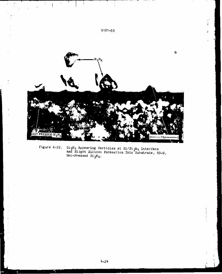
St-3N 4 Appearing I'art iote:_ at St/St_INII Intcrfaoo and_lighl: L4iitoon Porllioat ton ]iito SubDtr,ii.l,, SD-_),
Ilot -I'rc:;:_t,d SI..4N 11 ..................................... ll-i' 11
I'holotul,,l'oV, rdph of _l[|ootl Hi.oi"o_trtioturl'_ ,'4P-OIl,
Sil'i ] Eloh ............................................ ll-p!_
vii

I
._ .,,4. _..m,_.-_ ,,_.,L.4 .....4 • , °.H ........
4 -2 _I.
4-25.
4-20.
4-27.
4-2'3.
4-29.
4-5_.
4-31 •
4-32.
_-3q .
4-38.
4-3_.
4-40.
blOl-b3
ScatHllrW. Eh_ctroll Microscope l_hotomierogl'aph of (]l'ain
Boundary hnDurkty Phase, SD-{_II ........................ 4-2b
Photomacrograph of Sectioned Se.qsile Dz'op) SD-15,
Showlng Cracks in Silicon ............................. 4-27
Photomicrograph of Interface, SD-111, Near Edge of
Sessile Drop ........................................... 1|-28
Scanning Electron Microscope Photog1'aph of Silicon/
RS Si3N 4 Interface SD-14, S11owing ThiI: I.ayer ofIntermediate Bi Content ............................... I_-28
SiLico]10xynltrlde, Photomaerograph of Sectioned
Sample Showing, A - Unreaeted Teat Surface,
B - Reacted SurFace (Silieotl Wicked in) and
C - Silicon Drop ...................................... 4-31
The Si3N 4 _ AIN - A120 _ - SiO:_ System }_ased onResearcll :it Newcastle [Rel'ez'e_lee" 4-2b) ................ 4-34
_etting A_gle vs Time from Melt for Molten Silicon
(1430°C) on SI-AI-O-N Refractory Fk_terial ............. 4-35
Wetting Angle vs Time from Melt t\_r Molten Silicon
(1430°C) o_I Si-AI-O-N Refractory Material ............. 1)-30
$D-30 i_' Phase Silieon/Sialon Interface Showing
Some Evideuce of Grain Boundary Precipitates and a
Relatively Clean lhterfaee ............................ 4-_
}_ Phase _ilieon/Sialon Interface, SD-30 .............. I_-3[_
Scanning Electron Microscope Photomicrograph of _' Phase
Sillcon/Sialon Interface, SD-30 ....................... 4-3_
Seam_InF. Electron Microscope Photomierograpl_ of Graiu
Boundary Impurity Phase in Silicon, SD-30 ............. 4-30
Energy-Dispersive Analysis of X-Rays (EDAX) ........... 4-40
Silleon/]SR Si_gle-Pl_asc Sialo1_ Interface, SD-57,
alld Silieoll/15R Polyphase Sialon Inte1'faee, SD-59 ..... 4-I_0
Impurity Phases in Sillenll Molted oll Sialon
Material, SD-Sq, as-Polished .......................... 4-41
'typical Polyphase Sialon blaterial, SD-{_O,
as-Pol ished ........................................... 4-_! ]
Silieon/Sialon In,err'ace, SI)-O 1, Showing Aluminum-Type
Impurity Phase in the Silicou ......................... 4-42
viii 1

i i
b 101 _+)3
1|.111.
4-42.
4-43.
4-4 I1,
4-4 5 •
4-4o.
4-47
4-48.
4-4 Q.
4-50.
4-51.
4-52.
4-qb.
YllotomacroF, raph of Sial on Subst,'ate, SD-(Y), SllowinF,
tile Sop;wilted Sill,}oil Se_stLe Drop and a S(,etional
Mfcrograph of the .qtl. leot#Sub:q.rifl.e lnt.et, faot .......... 11-112
Contact Angle tl vs Cotlt,aet 'L'itl)t" f+OP Mol. ten Silicon
on _apph [l't ............................................ lt-II 4
Photolllael'Ol,';l'dph or S_Li_'oll oh Sapphll'e_ SD-Oq alld
+l'l_'[ 0 .................................................. 11-115
l,:tyel" told P+lel. t. I_eai_t LVit, ie,_ vs Aceumul at ed Time
That thc l_espeetJve Heltq ,,,+ere l.:×l.+o:+ud tO Ntll. 1..itrk ...... 4-ILL]
SkLLeon on Carboll-Coat, ed Muttite Sub'q.rate
Showlng For'uat. totl t}f St(+ Particle:; .................... 4-4g
Scct. ionat l,ticrol.,d'aph of SJl. icotl/Hul_l |to ll'tt.el'ra<'e ..... il-h 1
EnLarged Vi.ew or Area I, Ftgure 4-4b, 8howin_ Nat,,n'e
and P.lorphology or hlllXtrtty l'hase_; ..................... 4-51
l.]ILart.',ed VLew of Area J, F'lgtlr'e .+I-40, ShOWlAltr, Nattwe
of Prcci.pltdtes Nc'ar lilt.el'Face; Sll'3peeted ella+(? |.+
SIO 2 .................................................. 4-52
Scanning ELectron Htcro:_eope PhotomLcrograph
Showtnt: SlltconlHullite Intel'faee and PrectpttaLe:_
tn Silicon l't_trtx ...................................... 4-52
Sect.lena1 Htcrograph of Sit icon/HullJte Interface,
SD-40, Showing Silicon Penetration Into Mullite
Porosity .............................................. 4-%3
St}. icon/Silica h_tert'aee )\)r Fused SLliea, SD-5I+,
and S+ttp-Ca._t Stttea, SP-!_O ........................... 4-',b
PhotomacrogPat.)h of Black GLass SD-48 Showing
Sub:+t.rate Stll't'aee GlaZing and Separated _ilieon
Sessile Drop ........................................... 4-57
Si.licon O)I }!l..lck GL:'Is:_, SD-IIL+ .......................... 4-56
PhotomaerogPaph of SflLeon SEssile Drop at_d Ilot-
Pretmed }IN Sub:q,t'ate, SD-IO ............................ II-bl
lifo 2, .ql)-3i.:, Post-'Post, Stir face Corm i t.ion Sitowing
Ab-mnce of Silicon, Huderaoking Pattern in CVD
Layer Ahd Stlb_tt'ate C)';:cRs ............................ ll-b_
Plloton)aorogPaph of Silicon on llfC, SD 3.t ............... It-b4
}IrC/Silieon Dlterface, As-Polished CondttLon .......... 4-05
ix

5101-53
4-58.
4-59.
4-60.
4-61.
4-62.
4-63.
Top View of Silicon on Y203 , SD-31, Showing FineCracks Emanating from Silicon Sessile Drop ............. 4-66
Sectional Macrograph of Silicon/Y203 Interface, SD-31,
Showing Penetration of Silicon Into Y203 Substrate .... 4-66
Silicon Matrix, SD-31, as-Polished .................... 4-67
CeS, SD-73, Showing the Post Sessile Drop Test Surface
and a Cross-Sectlonal View Showing the Extent ofSilicon Absorbtance and the Dimensional Change inthe CoS ............................................... 4-68
Sectional Mierograph of the Reacted Si + Ce + Sand Unreaeted Ce + S ................................... 4-68
LAB6, SD-74, Showing Silicon Material Adhering
to the Substrate and the Remaining Si/LaB 6 Interface -- 4-70
I-I.
I-2.
Materials Tested for Stability With Molten Silicon .... I-9
Reaction of Possible Die and Crucible Materials With
Liquid Silicon ........................................ 1-10
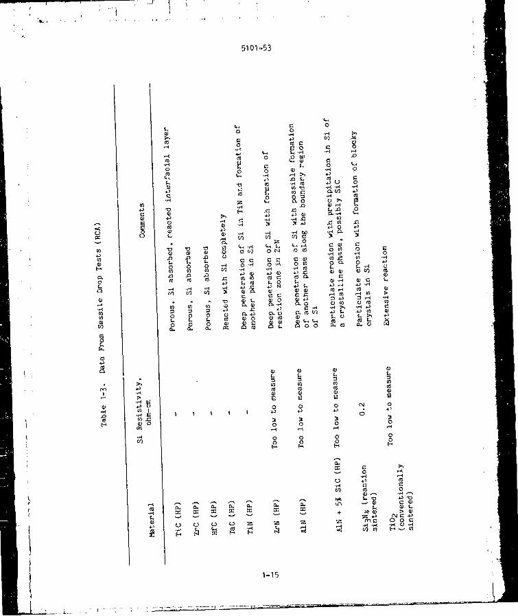
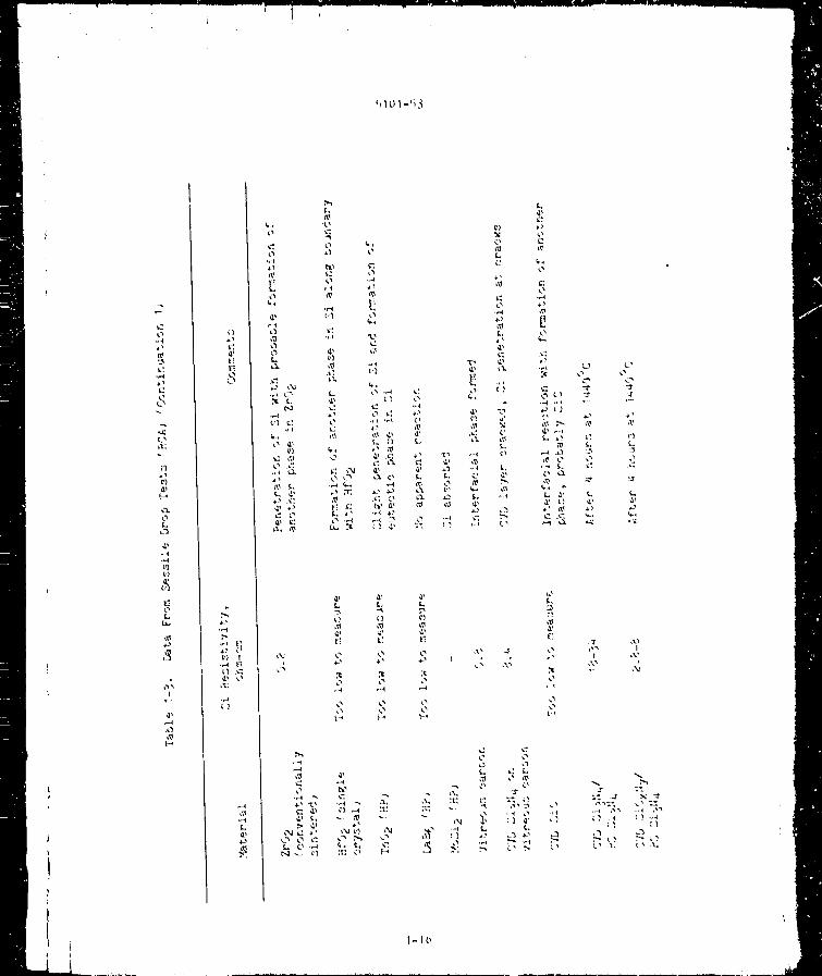
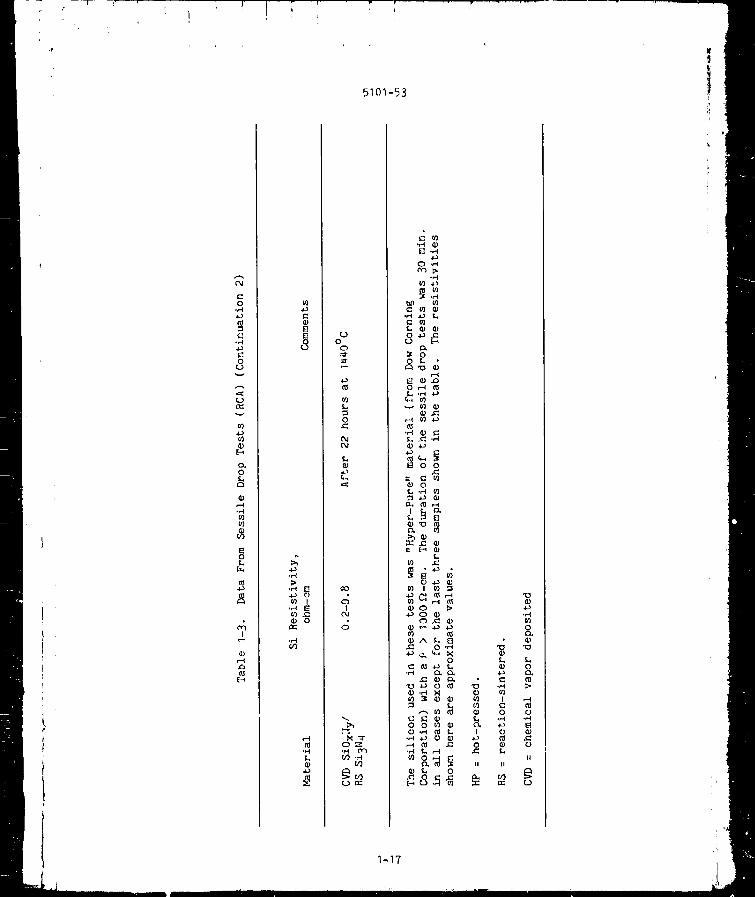
I-3. Data from Sessile Drop Tests (RCA) .................... 1-15
I-4. Concentrations of Unintentionally _dded Impu_ities in
Typical Czochralski Silicon Crystals .................. 1-18
I-5. Qualitative Behavior of Metal Impurities in Silicon --- 1-19
I-6. Segregation Coefficients ............................... 1-20
3-I. Test Refractory Materials ............................. 3-I
4-I. Semiquantltative Determination of Impurity Levels in
Silicon Melted on Various Refractory Materials ........ 4-11
4-2. Typical Chemistry Data Si3N 4 Froducts .................. 4-19
4-3. Various Sinterlng Additives to Silicon Nitrldes ........ 4-20
4-4. The Emission Spectrographic Analyses of Various SiliconNitrides .............................................. 4-29
4-5. Sla]on Material Processing Variables .................. 4-33
4-6. Emission Spectroscopy Chemical Analyses of VariousMullites .............................................. 4-46
. ) i
4-7.
4-8.
5101-53
Typical Chemleal Analysis of MeDanel MV-20 and MV-30
Mullite ............. _.................................. 4-46
Typical Chemical Analysi_ of General Electric Type 204 4-54
Fused Silica Tubing ......................................
i
xi

5101-53
SECTION I
INTRODUCTION
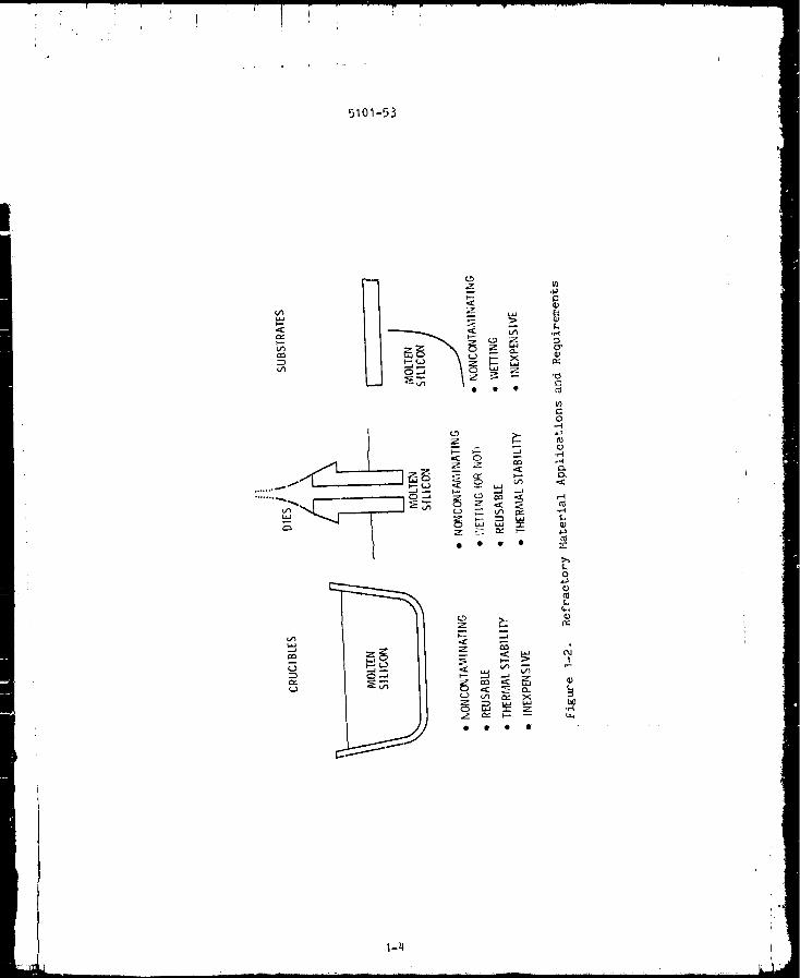
A. BACKGROUND
The JPL Lnw-Cost Silicon Solar Array (LSSA) Project was established
with the goal of decreasing the cost of solar arrays by improving the
technology and by increasing production volume. Silicon solar cells have
widely been used for generation of electrical power in space and have
found some limited uses on Earth. It has been proposed in recent years to
use silicon solar, cells for' the routine generation of electrical energy
for commercial use; and the present energy crisis has placed renewed
emphasis on this proposal.
The major shortcomin£ _ in the use of silicon solar cells for terrestrial
power generation are the expensive proeessirg in terms of equipment cost,
the large energy consumption during growth, and the lengthy and sometimes
wasteful processing needed to prepare solar-arrays (Reference I-I). Con-
siderable attention is therefore being given to the problem of developing
be.,ter methods of processing the cells. The present method of w_fer-
slicing and polishing of Czoehralskl boules into cells is very inefficient
in terms of percentage of a single boule which can actually be produced.
Several potentially economic processes are under consideration. One
such technique that shows great promise is silicon ribbon growth, which
includes such processes as edge-defined, film-fed growth (EFG) (Reference I-2),
web dendritic growth (Reference I-3), inverted ribbon _rowth (IRG)
and laser zone growth in a ribbon-to-ribbon (RTR) process. Other silicon
technologies being investigated include the dip coating process on
low-cost substrates and ingot growth by the heat exchanger method.
Most of the programs being supported under the Silicon Material Task
and the Large Area Silicon Sheet Task of the LSSA Project involve the
manipulation of molten silicon. In several cases (e.g., edge-defined
film-fed growth and inverted ribbon growth) such hlgh-temperature materials
for use as shaping dies appear to be the limiting factor in the development
of the technique. In spite of the importance of this, only minor efforts
have been made to evaluate existing materials and to develop materials
for this purpose and for use in vessel_ to contain and transport silicon.
Generally, results which have been reported are inconclusive, primarily
because cf the failure of the investigator to properly characterize
and eoeument the history of the materials being evaluated.
There is a pressing need for materials evaluation and development
programs by which various hlgh-temperature materials may be processed
and evaluated for their use as components in direct contact with molten
silicon. Molten silicon is quite corrosive even to the point of being
labeled a "universal solvent." A major problem with molten silicon
contact material is dissolution, which results in both detrimental level
impurity contamination of the silicon and changes in geometry of the
refractory. There are indications that recently grown EFG silicon
ribbon approximately 7.6 centimeters wide at 7.6 centimeters per minute
is limited in efficiency by unintentionally induced chemical impurities
I-I
: li
5101-53
with res_stance-furrlace-produced EFG material (Heference I-_).
Depending on the speclfie application, there are many other requirements
for molten St contact materials besides very low reactivity. For example,
die applications require substantial wetting by molten silicon to draw
ribbons by capillary rise through a partially immersed die (Figure I-I).
The existence of such generally opposing requirements of good
wetting and low reactivity poses obvious problems. Potenti_l problems,
however, are not limited to wetting and reactivity. For dlp-coated
substrates, matching coefficients of expansion with silicon becomes
important in order to avoid cracking the silicon layer, and cruelbles
used in the heat exchanger method must exhibit a lack of bonding at the
ingot wall surface to prevent cracking of the silicon ingot during
solidification. Silicon will expand approximately 9% by volume when it
solidifies. Some general applications and requirements for these refractory
materials are shown in Figure I-2.
In view of the importance of high-temperature materials to the
success of Low-Cost Silicon Solar Array (LSSA) Project, JPL initiated
an in-house study of the compatibility and wetting of silicon on selected
refractory materials. This report is intended to bring together all
the materlals-related problems as they pertain to the production of
quality silicon for solar cell applications. It is hoped that this
will lead to more detailed consideration of the specific material developments
needed to produce cost effective cells useful for terrestrial applications.
B. WETTING BEHAVIOR
One of the oldest, most useful and convenient means of measuring
wettabillty and obtaining information about interfaclal reaction is the
sessile drop experiment. Even recently, many have used this experiment
in evaluating llquld-solld-vapor material systems (References I-5
through I-9). Quinke (Reference I-I0) made the earliest use of the
sessile drop method to determine surface tension.
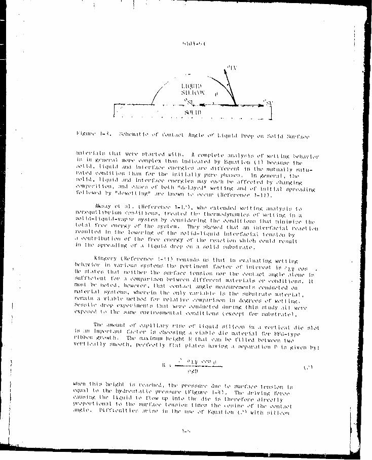
The wetting of a solid refractory can be quantified iD terms of a
wetting or contact angle O, which is the angle formed by the tangent to
the liquid surface at a point of contact with the solid (Figure I-3).
Complete wetting occurs when _, = O, partial wetting when 0 <0 ! 90o and
nonwetting when at _*> 90 °. Industry experience in ribbon growth
techniques has indicated that a contact angle of less than 80 ° was
required for stable growth in capillary action shaping techniques.
The contact angle of a drop of liquid silicon resting on a flat
substrate is determined primarily by the equilibrium between the surface
tension of the solid oSV, the surface tension of the liquid _LV, and the
solid-llquld Interfaclal surface tension, _'LS. This angle is determined
by the relative magnitude of these three interfacial tensions.
°'SV : _)'LS ÷ (,LV cos U
Equation (I) always opplies as long as o SV , 'rLS, "LV refer to the
conditions at the time of measurement -- but not necessarily to the pure
I-2

5101-53
RIBBON
CAPILLARY
DIE
MELT
CRUClBLE
Figure I-I. Schematic View of Edge-Defined Film-Fed Growth (EFG)
I-3
j
5101-53
Z
Y_
_ 1z - _• • •
zm _ m_- w- -J
CD
z z
I
z _m m
0@@@
0
C"@
0*r-¢
.rg
C_
0_._
0
0
O_!
0
_0
1-4
',_t) I-L, '1
I,'iKul';' 1- 4.
• "1VI.
//' I,It!U I/)// ,_il,i,'OX ,, \I l
_k'lh'lll_l| i_' o1' t_i_llt;l_'t AII),',I'(' O r l,iquld IIl'Oip Oil :tol'ld ;:,ul'|'_l_'l'
Ili_lll'i'l,l|;_ Ill,it Wt'l'l' ';l_ll'ted with. A ¢Oili/plet_' _l_,lly::i:_ <'i" welt t.ii.i4 l'eh;I7|_'i"
i:l ill l.;l'l_.t'l'_ti Illol't' _'ot'll,_iex t l'l,tlt illdi_'_ted by l'_qllltl toll { 1] bt, el,,ll.._e I I_l,
:_olld. ltqllld ,liid illlel'l',l_,e eilt'iw._le:; _l'e dil'l'l,i't,lit ili file Iniilii_illv ;_:ilii-
I',llt'_l t_,_lhIltl loll ill,ill I'o1' the tllili,ll,iy t'tll'l' l'll;l:lim. 111 i-h'liel'_ii, lhe
:_olid, 1iqlitd ,tlhl l,lll.,'l'l',l_'_" I'lll'l'F. lt':_ Ill,I)' t'il?h Di' dl'l'l'l'l'l'd 1_)' _'ll,ill#.(lllF.
,'<'llll_<':_l! tc'll. :llld e_l;_e_ of l,,l, til "d_./il)'ed" wi, l l, trl_; dlld oi,' it111 l;ll :_l_l'e,ldilll_;
l\,l l<,_<.<l, i,)' "dewett I(l_ li .l.lit' Lllc'Wl/ it' <_t't'lll" (l'_t'l'l'l't'llt'l' 1-1 1).
Aki_,ly I'l ;ll • {)h'l'l'l't'llt'e I-i'.'). k'l'li' cxlellded Icetttllt_; _ill,li)'-_t'_ Io
II_lh'qutlll,_l'iillll d_.!),!il ioli,_, l,re, ill>d lilt, l,hl'l'iiiodyli_ii;l{d.'_ _,I' w_'(l ill F, ill it
:lol {d-I l,qlll,l-',';ll_ _1' :i),:;l I'111 II) ' <'Oll:lldi'l'illK { li_' _'<_11_i'l I iOll:i I' h;tl Ill ill i lili;tO I l'h'
tol'ill l'l'l'l" i'll('l'_), Of the ,tt t¢'ll'('lll° Th_')" <.lho/_'ed ltl,II _tll lll/t'l'l',tt'itll I't',/Ot loli
l'e:llil,l,ed Ill l,hl" l,ol_'el'lll_; of Ilie :;olid-l'iquid ililerl',lei_li tOll:_ion b)'
,I _,_llll, ll_lll iOli oI' il,h' fl't't" t'l/t'l'_{)' O|' lhl" I't';IOllOII _.'l'_ii_'h OOtll. d l't'ntl'll
lit {lie "_l_rt',idl,ii_.; of' ,I liquid di'op _ll ;I :_olld :_uimll'.tte.
l_lii_;el')' (17el'erl, ih, t, 1-11) rt.lllitld._ tl:; thlit in ev_llu.lli,l_ wetttni.;
Dt'h,:vior in \',ll'i,,u:_ .-t)':ttelll: _, the th'l't ilioFIl ILl_'tOl' _I' liltel'e:_l i:_ "I.V c'O:_ .
l'tt" lll,llt'l'_ ll'l,ll llt'illlt'l" ll'll' -"IUl'i'(/Ot TM lt'l/_iOI _, llOl" It_t" <'Ol//,tk'l _lll_lt' .l!l_lll ' i:_
,_Itll'l'l_'il'lll, l'Ol' ,1 c't_111)_;ll'l'_ioll l"l'il,.'t'_'ll dit'l,'i_i't'lll III;lit'l'i;ll._l i._l' t'l'llhl[l' it_lltl. It
lllt):_l l,l' Ill_l, I'd , llt'WeVt_l ' , t l'l_lt t't_ilt,itl'l' _lll#;l_t" Illt, iUllll't_llll'll| :I i't_llll'ili'l t'tl Oil
lii, tlt'i'l,tl _'_)':_it'iii;'_, v,glt'l'_'{i/ iht' <_II1%' vm'i.l/bl_' l.'_ If'It" _'ilil_'_li',lll" lll<Ul'i'l.II
i'ei'<i;ll'll ;I vt,llbit' Iileihu, d I'_1' I'el.ll Ivl' ,h_llll_ll'l.'i_ll l'li dt'_;l'¢'o:i _'{' Ice_.l lliy;.
Dt',+_:_iit" dl'_p I'_l_('l'illil'lll:_ litilll Wl'l't" <'Olidll_._l_'d dill'iHt4 ll'li.:l .':ltld)' Jill I,_el'l"
I.v_)_O_It't I, i i_ I lit' .'-i, lllll' l_llV i I'_111111'II I' it I' _'l_lhl i { t _ll:l ( t_.'_t't'l_l ('OI' -'Itl{_:li I',1( t' _ .
The _illlOllill o|' e,/pil L_t'.v t'i.':e c,t' Liquid :;l|lcot/ ill ,t vel't t.,_tl, die .'_tot
1_ .111 tlnl\_l'l,ilil, l',i_'ll_l' _.'; dhoo:_llll( _i '¢i_11,_i,_, die Ill, llt, l'till I'Ol, l,.]l.'cl-t),i_e
I'l,bl_ll F,l'Ottl h. 'l'h_' lli, l_illltllll Ih'lb',lll ti Ih,II oill/ be l'il le<l hell, eel,. l_,
vei'l, ie_ll,I)' .'IIllOO{_1, th't'('l'<'l I)' t't:ll, t_l'.ll,l':_ h:lvll_i_ >, ,t _lI,p:lr,ll, i<_ll D i.'_ ,_11ven Iby:
II _ _,'
wlll'll if,Ill; l,l_'l_hl, t:_ I'e_t_'hed, II!l, l,,l'e:;:tlll'e dlle |_' :_lll'l'.i_'l" ll'li'li_ll I'.<:
i'qtl_ll tO file IIvdro-;l,;It. le l,_l'l':mtll'l, tl.'t,_;ul'e 1-11), 'l,'lil, di'lvlill_ I,'o1'<'o
_'_lti:_l,ll_._ Illl. l,lquid Io flow up ilil,_ II,II-. ,.lie I:_ l,)ll,l'el,'oi'l, dire<'l,ly
,lll_(l'l'. l'gl'l't<'til'l it"_ ,ll'i:t(' ilt Ihe I1::1' /_f" l")_l,il.ll, l'_li ."_ wilh :;ilid_ll

5101-53
l)
_L
2, I _ _ o_H
Figure I-4. Rise of Liquid in Capillary Die
since the solvent action of molten silicon causes impurity elementcontamination which may appreciably change its surface tension.
Assuming that a given die configuration is capable of producing
and maintaining a capillary colunn of silicon I cm x 0.001 cm to a height
of at least 2.5 cm and a °tV for silicon of 720 dyne/cm (Reference 1-13),
wc can calculate a required contact angle O:
HPgD_ i cos-1 -- (3)
2 OL,V
0 i 87.73 c
It is interesting and important to note that even a 50% decrease in
the silicon surface tension (_rLV_ will lower the minimum required contactangle to only approximately 85.5 _. It appears that any material exhibitingeven slight wetting characteristics has potential use in capillary die appli-
cations. However, in allowing for imperfect die surface conditions (i.e.,
roughness), a minimum required contact angle of approximately 80 ° hasbeen used as a criterion.
C. _FECT OF IMPURITIES IN SILICON
The unintentional contamination of molten silicon with detrimental
levels of impurity elements is believed to be a major limiting factor in
attempts to reach the theoretical photoeleetrlcal conversion efficiency for
silicon (a_proxlmately 22%). Mobil-Tyeo has concluded, after many experiments,that chemical impurities play a significant role in degradation of conversion
efficiency in EFG ribbon material. In view of this factor, programs to
investigate the effects of various processes, metal contaminants, and
contaminate-process interactions on the performance of terrestrial solar
cells are in progress (_eferenee I-_4).
I-6
i
,_OIAI' veil I_L'I'I*oI'Illi|IIL'_" l,_ ,'H.l'OIl_ly lll|'lLIt'll_'L'll l'_y 1, hi" Ildt.lll'l" dlld
IhLV_' I't'lD. tcd _'l'l | |_t'l'l'Ol'llldtt_'L' tkl tot;ll IltL_dZlill't'd llllt_t, ll'lty _.'OI|I_.'IIL ) l}{tllOIl_._h
|It l';h'( tllC {ItlI_III'Lt_L_', _, Ill;ly bt' l_l'C,_t'llt l.II II V;ll'4, ety Ol" l'O1'1118 _lk'h ;I,'_
}_l'e_'|p_.t_lte,'_ o1' k'OltllxleX._',"_ O[' d|l'l'el'lll_ ,,leetl'l_,;l[ ohill'ilk_tCl ' . The _'{nl_l¢,
_'}_'k'tl'|_'dl. _'l'{'ect oI" ,_¢V¢1';11. d}l'l'el'Cllt _'l,_'l{lellt,'_ l:; _._11o_11 _.1_ l.'l,_lll'e 1-!_.
CqHd_, t,t', | [_IMII ,uld that only 1 ppb of t Ltdll_lllll _l] ,"_LI[_,'_._II _:4 _.'dl'_$1[_,' Of I'L'_.III','_LIiF ",
_.'t'll '[Z_ _1 l'-_yl_' "_.l_c'Oll hdv_tl_, dtl dL'_?_'l'tOl" k'Oll_.'L'tlt, l'dt LOI| _ll the ;',_, X 1015
to ':.0 × I0 I'' dtOlll:I,"_,'Ql',lll_,_"(}(_'I't"l'_'llk't' 1-1ll),
_'_'etltly) .'_l_e_'tl'O_itb, Llk'., .%y|ttldt', L'altl'Ol't_td (Ihq'el'Cth, e 1-1'_),
l'dbl'[¢,ltL'd _) ::_l'|',;ll'dLt"lOtS Of .'at._.[,..'Oll_tttl_]Ct_ tlltO _h.'_[iH',,.'C[_.._ll.'_[l]_
_'_I_VL'I_.[OII;_I ,'_L'I'O.'_I'q_L'L" t¢,'chltOloF_y, The" _'l'l'_'_'t of _IIL_WII [tlIDlH'lty L'L_IIL'I'I] -
tl',Lt+.otl: -t Oil :?-hOl't-L"[t'¢Lltt t'llt'l'l'llt dth| Cl'l't+,'_,l'llCy N[I_ tlIVe,'_tt_;'.ted. It
,_pl, e;tt'ed that the I_I't'._¢.'I1L'L" Of _?OI'_'L'I' ;_.'tl'_ tO neutr:]lt-;e t.ht" harm£ul
t'l'|'t'ct :_ Of ot ht'l' COl|tdtll[t|dltt :_. I'l't'[ tm[n;ll'y _;tt _ .'4tl_t,.,-_t _ t h,lt oopper m,ty
bt' ;h't tllp_ ,t_ ;t "p_ett.el'llt_," _'t,_t'llt or' ttlll_tll'tty _,tlk dlll'[ll_, d_.t'l'tlStOtl
l,l'oee,';:',tl_,),) whet'eby el'feels of detrLme|_ta], +Llttl_+.ll'lt, tc_ {t',_,.) t[tdlILllltt_
;tl'¢ Oft'Set. lX':;:'Lble :'yltcl',_',i,_'t _¢ el't'cet8 of v,+H').,,tn_ "+[llll_Lll't+,y i. O'Letttellt8
in :_tt't,'ott at'o ;Ill ;l|'t';_ _t" _l'e,lt tnteve:',t.
It. K. ILttes and t'l, 11, I.eipotd _l(et'_.'l'CtlL'¢" 1-10) haw' h;xd _ome
l_l't'[tll_llldl'y CXl_t'l'tClh't' w[[h tit'," Ill[tt_'l'l;11=_ l'Ol' t';F'G _l'oWth Of ,milt_'Ol_.
In ex,untntn_, the element;_ m;ttez'ial._ with _ut't'tctently high mt, Lt tn_
F.._tut_ (sh_wt] in 'l':d, le 1-1), they t"Otlth| that ;_11 of the vct't'actovy
:rod tv.m:_ttion met,_ts reacted wlti_ stlt,'o=_ to l'ovm a varLety of stlteLdes.
In nil the:_e systt,tt)n, the hLKhe:_t sltieide Li.e.. the one eont.;_tntn._
the Ilk_,ut _ttteon_ (,,vmed a euteette with _tlte,m. Thus, the_¢ ltl;_tel'[;_l_
Apl_edl ' to be t'xOltldt'd _['t'ottt _'Ol'+'_tdet';'_t+.ot_ _in_'e they would t'eaet with
,ltld dL:=,"-otvo ill stttoot'+, dot',tl'Oyil_g it_ elt,etvieal pl'Opet'ties, tlowevet',
tt :_houhi be cmphn:_t:;ed th;_t in all ¢:]ses the test tnK done t'cp/'o,_el]ted
,w;_i|nbh, mat.erta[_ _md t',_bt'tcat +,on technique w_.th no attempt at opt tmt':.tn._
ehemi"try, Ill[Ot'O'.',tl".|Cttll'e, Ol' dell6[ty. '|'e_t.'_ wtth the_e |_t'e]ttUit_;ll'y
ttlAtet'L,ll+S +.lhitCdtt'd _iL' tO b_" the nlo_t _t;.'tblt TM o_/l'btde) _L+_NI 1 the tlto_t
st_xble nttt'tde :rod |h'O the tllo:_t :_t;_bl.e OXide." bt'_id¢ SiO',.
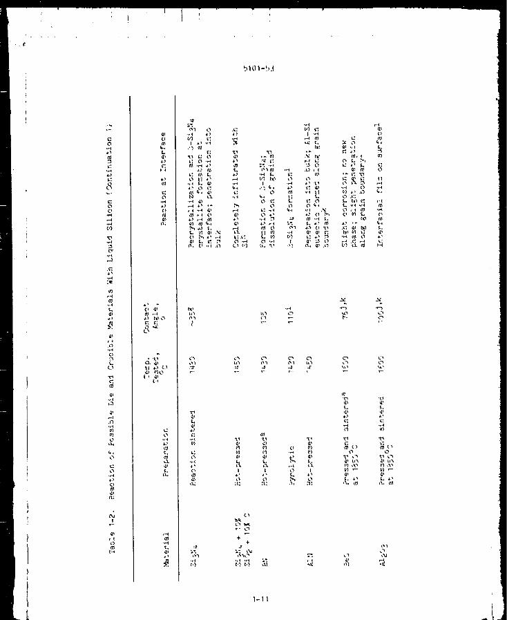
'l'Jtble 1-;', _omptted by IICA [,AbOl',_lOl'te_ Ll_e£++'t'enee I.-I?), e_mtain,_
eotttl\_tibtltty darn on the re,tetton.'; of po,,;stbte die ,rod evuoLbte
m, ttei't,xI:; with liquid sttteon. The ,"otvent :_atut'e ot" motten +'tricot;
ha:" been elt'+u'ly ob:;el'ved,
Ik'A l.abot'atorte+ has ,_t:'o had d++l'eet t'Xpel'Letl_.'e evaluat ttL_ dtt't'et'ettt
I'Ct't'++tetol'y tmttertn].,*_ t,:_ed in contract wtth ttlottel+= ,;t.Lteott (Ret'et'enee 1-l_).
Ill CV$1_lldt [t11._ ltlAtl'l'[;_ I, l'Ot' po:_tbte u:te in I_L'A's tlWt'l'tt, d t'tbb_,n p_l'owth
pvoee,u_, :t baste :_e:':_tte drop test w,1== _'Ol_dllett'd. ._tlb'G_'qtlt'l_t :_ecttotl_
or" tht't't' gt's,gt, le dl'ol++ Wel'e illldt)'?ed for +,'hl'lll[+.";l[ l'ed+2tiot_:; And t'teetl'l<'+_t
de_l'ad,d ton. 4-po tnt i+l't+_t + l't':; [ _t Ath'e tlt¢',t_tlt't'tl_t't_t.'_ Wel't" Ill;Ik_L + t+llt t hi"
V,iltlt'[l _ll't" Vel'y nl_l_i'oxim,ile. 'l'=_,ble 1-.4 tth,_ti',ite_ the d;It,'l ol, i,liill'd
t'l'oin th¢:_e tt':_ts. 'l'hc:_e te:'t:_ lihllt'_itt" the pott'i_i i_ll of L'VD SLjNI 1
dlkl 5tOxNy l_lAtel'l.Al ;trial othel'Wt:_e :_how the fOOl" l_l't'i'Ol'ln,_llh'e _l' d vat'lety
Of _'Otll Ik_ tlthlll.

5101-53
1 1 i i
•
L .1
_U!l,_l_q&/_. 'A.'IN:II:]1:1=13[13ZIIV_V_ION
0 _I.
oLt.1c"
.el
0 0
tal ._
I-t
@ @
.,-4 _
m .0
0 _
I
@
.rt
@
!
o
rd

l I I
_) 0 i -
Table 1-1. Materials Tested fer Stability with Molten Silicon
SiC Hot-pressed, polyerystalline Haselden Corp.
HfC Hot-pressed, polyerystalline Haselden Corp.
WC Hot-pressed, polyerysta.tllnc Haselden Corp.
AIN Hot-pres:_ed, polyerystalline l]aselden Corp.
TiN }|or-pressed, polyerystalline Haseldcn Corp.
WB 2 llot- pressed, pol vcrystal Iil]e Haselden ¢erp.
MoSi 2 Hot-pressed, polycrystalline Kantlml Corp.
Si3N 4 Hot-pressed, poiyerystalline Cel,ac/Pure Inc.
BeO Pl'essed alhi sinteped Bl'ush-Wcllinan Corp.
'rhO_ Pressed and sintered llaselden Corp.
ZrO 2 Pl'CSsed and sltltered Haselden Corp.
Y203 Pressed aE1d silltered Haseldell Corp.
ThSiO 4 Powder Cerac/Pure Inc.
ZrSiO 4 Powder Cerae/Pure Inc.
Only a limited number of materials have been used with any success
as dies or COlltaiuers. Silica is universally used as tile crucible
material for (Czoehralski) growth oF senlieolldtlctor grade silicon.
The concentration of unintentionally add_,d impurities foulld ill typical
Czoehralski silicon crystals is shown in Table 1-4. Silica is eom_ut, ible
with silicon, the solubility of oxygen in silicon being 2.7 x 10¹⁸
and tilt:liquid solubility, 2.2 x 10¹⁸ atoms/era3. Patel and Battermat_
(Reference 1-1q) have shown that hlgh-telnperature aging (1200°C) oF
crucible-grown silicon can cause clustering and precipitation oF the
oxygen incorporated during crystal growth. These defect structures
act as recombination sites (ReFerence 1-20), causing electrical degradation.
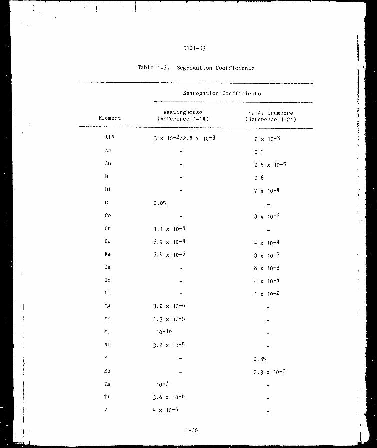
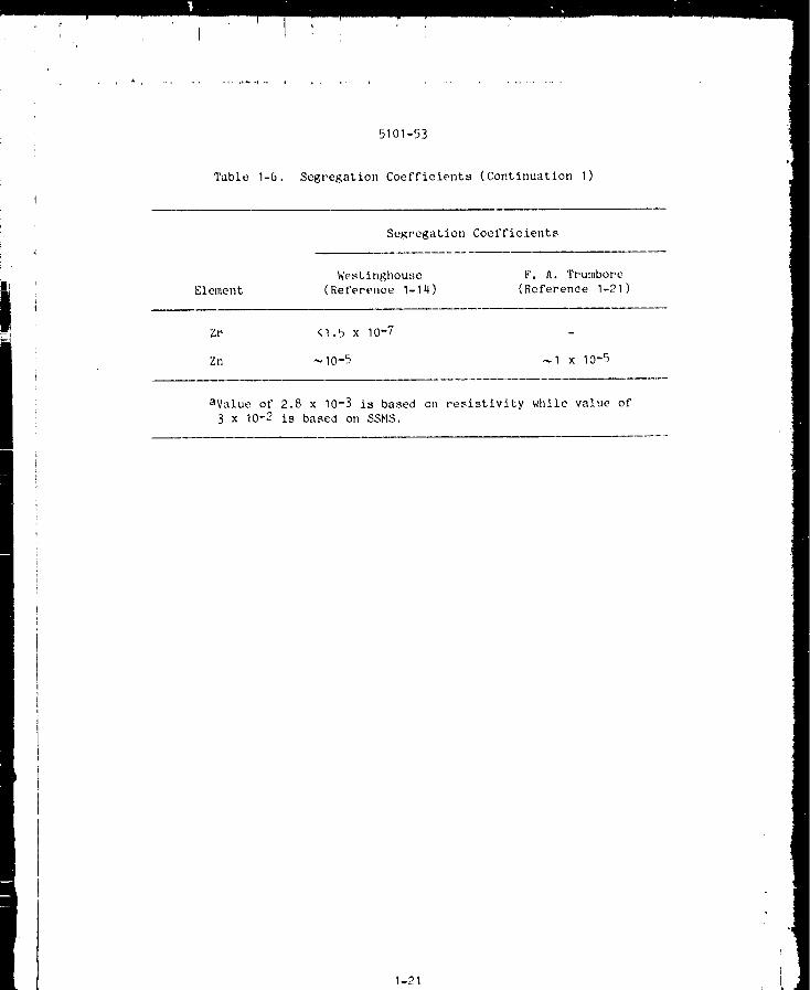
For general information, Tables 1-q and l-b have been included to
show qualitative behavior of val'ious metal imptn'Lties in silicon and a
compiled list oF effective segrcgatioll coefficients, respectively.
Much more work is needed to Fully characterize the el'feet oF
impurLties in silicon. 'rilerelation between impurities, F,cnerated silicon
structure and resulting electrical effieieney is in need of critical
evaluation.
1-q

.° 4
4
OO,H
r4.r4
,r473
'r(
A:
_g
V)
r-4¢0
L
,0
m
Q_
g_
,rl
0
0
0
i)
4_
_MI
_4.0
_DO
t_
_4
4_RS
V:O
O
8
d_ _0
t--,
0.,-4
0,1¢.,
_4
.e4
d_
0L_ "[1 0
1
_3 4¢ i {/} 13 _.)
(,1 |s., 0 0.; 'Es
:g ::I" ".1"
_s
OO
o
•,.--s ,.3
.L_ h) ,"* {t} _-1 .0 .a:
=1" -g ._,_ ".t :_
_1. t'l. 0..(_ I I _1 I I I
_ld ;Z:
1-10
÷ .t*%1 ¢M _M ;_.
c,) r,') _'1 (;1
i
b101-h3
O
D
00
.el
.el
¢)
Q_.'4
.0
.p,0
0
0
0
!r
Q)¢_
_H
0
o
O
t,
Q_
o'_ 0
g;
° t2_',geg
_ _'_ _.,
If; ¢_ ,_I .0
110
0
0
0
._. u_ _.
(/] hO 0 0
I.
,'_ 0 0 Oq_
,--4 e6 °_ o
O ,_ O ,H l _ D O
.-4
_I_ _I_
_) t'_ ,H _')
I I O I
0 0 _ 0
,4-+
,-4
l-It
_4Q_O
_ll, t {0
1,4 tx_ _
0 r4 _I .,-I
"O
_3
0
0
_M

b
0
:1
0
0
(J)
"0
,1
.-4:C
r4
.rd
0
L
_4
go
0
c_
_MI
0., ¢
0
¢1
,-4
L_
0
£.
iY,
, !
.,4
h101-!_3
¢
-'_- t'_ _., :_ ._"
J J _)
0
L:
_'_ L. "U _, _ _ _ ._ 0 ._
t_
",.0 _L_ _" ",_ -t _ _, _,/-
L
_'t ( "_ 1'} t')0 l') t_ (.) -t_
I-1, _
•, q _%J

h 10 1 -h .,_
o '1
. (
oL.'l
.4
'l.t
,H
.-°
:e
Lg_
• , A0:3
C_
., I
110Ct,
0
0
0
0
0,1I
i-
,.q
[4
c)
c_
4_
(,0 ,I
,t3. _:
0•, q
L.
,, q
(,) () ()
[ I C,} 0,] ,1,) L'_
LM t_ _'M
0",
<,
{.) t _
• e4 _11V_
.41
_3
L I"0
I
.J
)
0
00
(?
:3
_J
:-¢
u)
L
0
L_
e_
¢'10
0
0
C)
!
E_
L
g,
=
¢}
0 _ e)
L'_ • Lj;3
It, G_0 .(3
Lt_ ,J
= I
7 {,} ii
L
m
o
,_2
_)
o
_N%
0
_3
•r-_ I
¢_ _,
= I
• _%
L_
't_ (q
"0
=
_2
0
I--4
0.
¢0
L
_ 0
0
,-4 _
.2
bf_
_2 ,,_
0
et_
g ao
1_ f..,
0 ,r-I _.
O_ f-1 0
1-14
5101-53
CO
CO
0
,-4
CO
0L,_._
I
CO
0
.,-t
•,'t I._
.t-ICO ..
r._
J-4
0
L
o
oo
1,1 co _
g 2 _
I | I I I
0
,r-1CO
0 0 0 O_ 0
_o _o _o _o
0 0 0 00 0 0 0
v
0")
+
0
0
_rlc[
1-15
0
C
0 0 _
.,-'4
0
0
L_
0
I
@_4
Om_
.-4
.,._ _
-_4 t_l
L'L;
_, ¢'}
,_ _-. ._, '_. .,_
_,_ _ _'_ ..4 _
,--4
L
0
0
m_, kTM
0 k_
L,
q,-i-
f_,,
f...
I
.,_ ,_,-, .._ "_.
I-I(_
f
g:0.M
.M
0
CO
e.,0
3
rJ
0
0g.,e-,
_3
.M
No
I
m_o o
I
E-q
,M
0
5101-53
C.)00
0e_
O_
CO
0I
g
OZ•M or_
_0
UC=
,M
._ _._ _,
e._o
(g
I _ Cu
_*' _"
c_ 0 ',"_
0
_'_ .
0 0 cO 00._ • _
.M_ 0 0
@ _ 0
0
g/0
kI
.00
II
,..r,,
0
_o
I
0.M.to
II
n_
.M
0O,0
0O.
>
0
e-.0
II
e
1-17
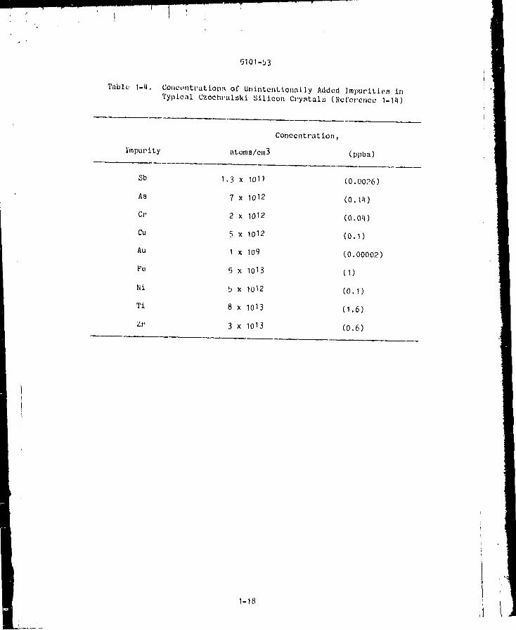
Table1-Jt,
5101-53
Concentrations of Unintent£onally Added Impurities in
Typical Czochralski Silicon Crystals (Rcfel'ence 1-14)
Impurity atoms/era3
ConcentPatlon
(ppba)
Sb 1.3 x 10¹¹ (0.0026)
As 7 x 10¹² (0,1_I)
Cr 2 x 10¹² (0.04)
Cu 5 x 10¹² (0.1)
Au 1 x 10⁹ (0.00002)
Fe 5 x 10¹³ (I)
Ni 5 x 10¹² (0.1)
Ti 8 x 10¹³ (1.6)
Zr 3 x 10¹³ (0.6)
1-18

i
i
5101-53
t-
oc
OO
.r4
.r4
.r..I4J
O
O
,1=I1)
.r4
.O
.M,-.4
g
!
O
NIC
e-,
O
4_
O
O
L
O
O
E
O,--I
OO
N?
0
B
o
0
IE
"0
1-19
I
5101-53
Table I-6. Segregation Coefficients
Element
Ala
As
ALl
B
Bi
C
Co
Cr
Cu
Fe
Ga
In
Lt
Mn
Mo
Ni.
P
Sb
Ta
Ti
V
Segregat _on Coefficients
West ingllouse
(Reference 1-14)
F. A. Trumbore
(Reference 1-21)
3 x 10⁻²/2.8 x 10-3
0.05
1.1 x 10⁻⁵
6.9 x 10⁻⁴
6.4 x 10 -6
3.2 x 10⁻⁶
1.3 x 10⁻⁵
10-16
3.2 x I0-5
10-7
3.6 x 10 -6
4x 10⁻⁶
2x 10⁻³
0.3
2.5 x 10⁻⁵
0.8
7 x 10 -4
8 x I0 -6
4 x 10⁻⁴
8x 10⁻⁶
8 x 10⁻³
4 x 10 -I!
I x 10-2
0.35
2.3 x 10⁻²
1-20
r
d
5101-53
Table I-6. Segregation Coefficients Continuation I
Segregation Coefficients
Westinghouse F.A. Trumbore
Element (Reference 1-14) (Reference 1-21)
Zr <1.5 x 10⁻⁷ -
Zn _I0-5 _I x 10-5
aValue of 2.8 x 10⁻³ is based on resistivity while value of
3 x 10⁻² is based on SSMS,
1-21

._t, _ i _ • _._i i,, _ . i , .
5101-53
SECTION II
EXPERIMENTAL PROCEDURE AND TEST SETUP
The basic experiment conducted involved measuring the wettingor contact angle of drops of molten silicon on various solid refractory
substrates at a temperature Just above the melting point of silicon.
Post-test analyses involved the measurement of the amount_ mode andmanner of interface reactions as well as documentation of phase and
chemical changes that occurred in the silicon or substrate during the
test.
An N-type, single-crystal, Czochralski grown silicon with a I-0-0
orientation was supplied by Wacker Chemical Corp. This material had aresistivity rating of 62-86 ohm-om. Silicon test samples were obtained
by diamond core drilling 6.35-mm-diameter coupons from the 6.35-mm-thick,50.8-mm-dlameter silicon disc blanks. These samples were chemically
cleaned in concentrated HF, weighed and stored in a desiccator.
Refractory substrates tested varied in overall size and thickness
but were all mechanically ground to provide flat, parallel surfaces andpolished to a 15_ finish, unless otherwise indicated in data tables.
Each substrate test surface condition was documented at 40X magnification.The refractory test samples were vacuum-furnace-baked at 240 _ I0°C
for approximately 2 hours, then weighed and stored in a desiccator.
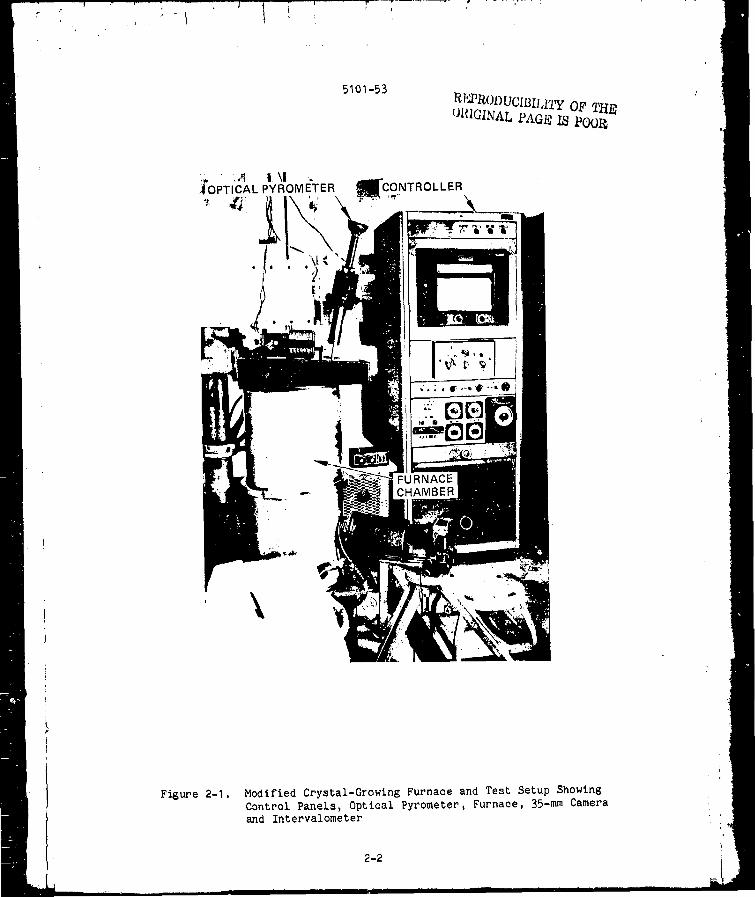
In the laboratory tests all silicon and refractory substrates wereheated to 1430 _ I0°C in a modified crystal growing furnace (Figure 2-I)
with a flowing helium atmosphere and allowed to stabilize for 10-15
minutes. Then photographs were taken at 1-min intervals for time periodsvarying from 20 to 35 min. Helium in silicon has a calculated diffusion
constant DO of 0.026 em2/sec and a solubility S (atm-1 cm-3) of 6.5x 10¹⁴ exp (-11000/RT) but is electrically inactive in silicon (Reference 2-I).
A motor-driven 35mm single-lens reflex camera with bellows extension
and a 135mm, f/2,8 lens with a neutral density filter (ND.6) (Figure 2-2)
permitted 3/4 - IX magnification photographs to be taken at selectedtime intervals through the use of an intervalometer. Subsequently,
visual measurement of wetting angles were made directly from enlarged
prints of selected frames, using a protractor (Figure 2-3). Kodak
black and white films Tri X, Plus X, and HC-110 were all used successfully.
HC-110 gave the best contrast results.
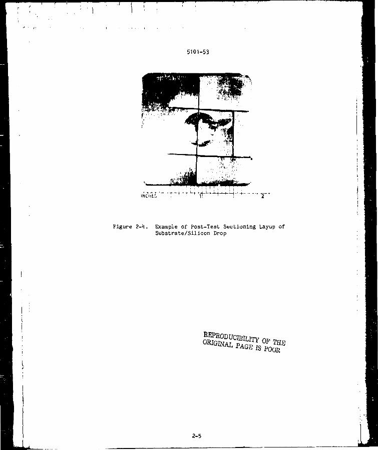
Post-test analyses required sections to be taken through the
solidified sessile drop/substrate (Figure 2-4) and mounted for material-
lographic studies. The results of those studies are discussed within
this report for each class of material.
2-I
5101-53
,_OPTICA L PYROMETER.'_C_ONTROLL ER
\
Figure 2-I. Modified Crystal-Growlng Furnace and Test Setup Showing
Contrel Panels, Optical Pyrometer, Furnace, 35-mm Cameraand Intervalometer
2-2

|
2-3
o
0 tO _ _.,_ _ 04J
0
,_ _ .,.._
,._ ._1 .,,...I
•_ _ I _
bOO
_00 b_
._ _ o _.
-_._ _ _ _g
{:_-.0 _ _ "
!
'i

5101-53
I-'_ 0.5 cm----_
Figure 2-3. Profile Photograph of Liquid Drop of Silicon
(1430 ±IO°C) on Slip-Cast Fused Silica Sub-strate. Lines on Silicon Drop Are Reflections
of Gaps in Surrounding Graphite Heater Elements;
Approx. Mag. 5X
2-4
.°
L
5101-53
Figure 2-4. Exa,_pie of Post-Test Sectioning Layup of
Substrate/Silicon Drop
REPRODUC_ILITy OF THSOR_[G_AL PAG/¢ ISPOOR
l
2-5

5101-53
SECTION III
REFRACTORY MATERIALS
The essential relationship between the processing of materials and
their resulting properties has grown in importance in recent years.
Refractory materials can now be produced in varieties and by processes
which were not practical a few years ago. Significant testing and
evaluation of these refractory materials for use in specific
applications, such as ribbon dies end containers for molten silicon,
has not yet been accomplished, especially to relate unique processing
variables with resultant silicon compatibility properties. The sessile
drop experiments conducted in this study are a first step toward
determining the compatibility of currently available refractory
materials with molten silicon.
Table 3-I shows the test refractory materials grouped according to
fabrication techniques:
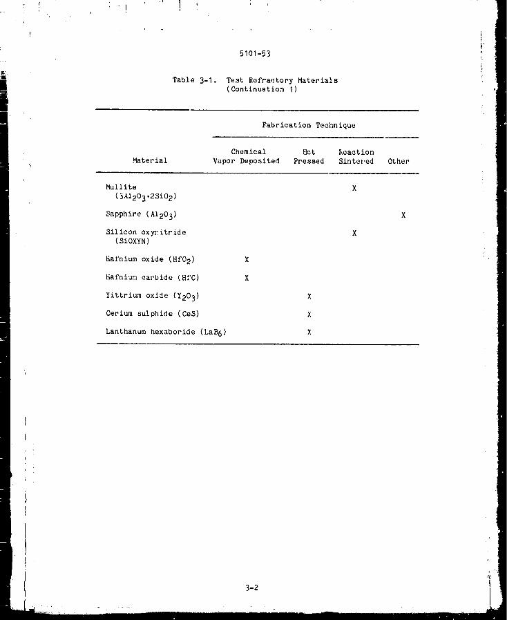
Table 3-I. Test Refractory Materials
Fabrication Technique
Chemical Hot Reaction
Material Vapor Deposited Pressed Sintered Other
Silicon carbide (SIC) X X
Glassy carbon (C) X
Graphite (C) X
Silicon nitride X
(Si3N4)
Si-AI-O-N X
(B', 8H, 15R and
polyphase)
Boron nltride (BN) X X
Black glass (C.SiO2) X
Silica (SiO2)
3-I
5101-53
Table 3-I. Test Refractory Materials(Continuation I)
Fabrication Technique
Material
Chemical Hot Seaction
Vapor Deposited Pressed Sintered Other
Mulllte
(3A1203.2SIO 2)
Sapphire (AI203)
Silicon oxy_itride(SiOXYN)
Hafnium oxide (HfO 2)
Hafnium carbide (HfC)
Yittrium oxide (Y203)
Cerium sulphide (CeS)
Lanthanum hexaboride (LaB 6)
X
X
X
3-2
5101-53
SECTION IV
MATERIAL CHARACTERIZATION AND TEST RESULTS
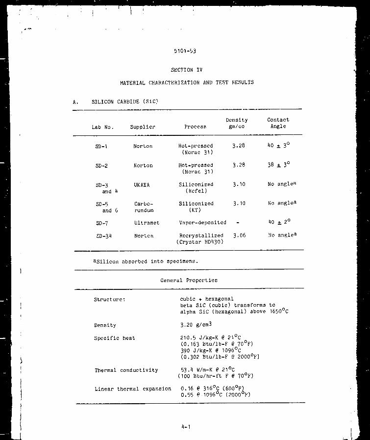
A. SILICON CARBIDE (SIC)
Density Contact
Lab No. Supplier Process gm/cc Angle
SD-I Norton Hot-pressed 3.28 40 ± 3 °
(Norac 31)
SD-2 Norton Hot-pressed 3.28 38 ± 3°
(Norac 31)
SD-.3 UKAEA Siliconized 3.10 No anglea
and 4 (Refel)
SD-5 Carbo- Siliconized 3.10 No anglea
and 6 rundum (KT)
SD-7 Ultramet Vapor-deposited - 40 ± 2 °
SD-34 Nortcn Recrystallized 3.06 No angle a
(Crystar HD430)
aSilicon absorbed into specimens.
General Properties
Structure: cubic + hexagonal
beta SiC (cubic) transforms to
alpha SiC (hexagonal) above 1650°C
Density 3.20 g/em3
Specific heat
Thermal conductivity
Linear thermal expansion
210.5 J/kg-K @ 21°C
(0.163 Btu/ib-F @ 70°F)
390 J/kg-K @ I096°C
(0.302 Btu/ib-F @ 2000°F)
53.4 W/m-K @ 21°C
(100 Btu/hr-ft F @ ?O°F)
0.16 @ 316°C (600°F)
0.55 @ I096°C (2000°F)
4-I

: i
5101-53
I. Hot-Pressed
Hot-pressedSiC(Norac31, SD-I, andSD-2)wasmanufacturedbyNortonCompany,Worcester,Mass.,by a fabrication techniquewhereinthe ceramicmaterial wassimultaneouslysubjectedto temperaturesinexcessof 1600°Candpressuresexceeding13.79x 106N/m2(2000psi).Nooxideadditiveswereusedto promotedenslfication. Thesubstratematerialconsistedof voidsandthreedistinguishablephaseswhichappearedto beSiCandsmallamountsof free carbonandsilicon.
a. Sessile Dried Teots. High-bulk density SiC (SD-I 3nd SD-2)
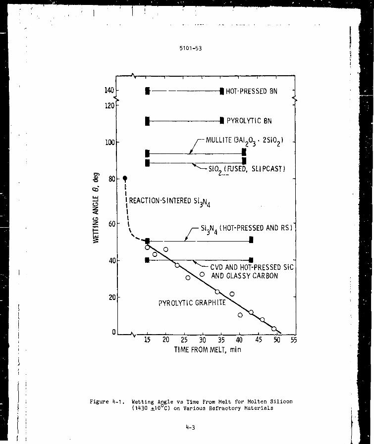
exhibited good wetting (.-40°, Figure 4-I), consistent with previously
published data (Reference 4-I).
b. Compatibility. Examination of materlallographic sections of SD-
1 and SD-2 revealed: (I) an interface that appeared clean and essentially
two-phase, silicon/SiC (Figure 4-3), (2) fine particles of SiC, 2.5 to !2.5
microns (approximately 0.0001 to 0.0005 inch) in size, distributed near and
along the free surface of the silicon drop (Figures 4-2 and 4-3), and (3) some
evidence of grain boundary impurity phases in the silicon matrix (Figure 4-2).
In the family of SiC products tested and evaluated, hot pressed
material seemed the most promising. Thel.e appeared to be fewer and smaller
SiC particles than had been observed in silicon melted on other SiC products.
However, the quantity of SiC in silicon solar cells that can be tolerated
without decreasing efficiency excessively has not been established.
2. Siliconized
Refel SiC (SD-3 and SD-4) was manufactured by United Kingdom
Atomic Energy Authority (U.K.A.E.A.) at Springfield, England, from
graphite powder and fine alpha SiC (Reference 4-2) which was mixed with
an appropriate plasticizer and formed into shapes by means of die-pressing,
extrusion or isostatic pressing. Through adjustments of graphite and
SiC contents, the amount of free silicon present in the final m_crostructure
can be controlled. However, fabrication techniques limit the remaining
free silicon content to a minimum of 8%. The fabrication process consists
of siliconizing, which occurs in a partially evacuated chamber, with
a green-machined part placed in a pool of molten silicon. Evaporated
silicon monoxide reacts with the outer surface_ of the parts at temperatures
from 1600 to 1700°C. The inner surfaces of the part act as a wlck
through which the silicon flows by capillary action, reacting exothermically
with the free graphite to form beta SiC. This beta phase bonds the
fine alpha grains together, leaving an excess of sillccn in a continuous
matrix through the structure. The Refel SiC used _n this wetting e×periment
consisted of a relatively fine-grained structure with roughly 30% free
silicon and 5% void content (Figure 4-4).
The KT SiC (SD-5 and SD-6) was manufactured by the Carborundum
Company, Niagra Falls, New York, and was formed by a method similar
to Refel. Mixtures of graphite and SiC (Reference 4-3) plasticized with
carbon-bearing binders arc formed into a variety of shapes by extrusion
or pressing. This material, after curing, is he_ted to between 2000
4-2
!
5101-53
140
120
i00
_' 80
(DZ
(,.9_ 60
E
40
20
0
I I I I I I
1 HOT-PRESSED BN
I -•PYROLYTICBN
t
s MULLITE (3A1203. 2SiO2)I , •i im •
• L SiO2 (_FUSE_, SLI PCAST)
I
IREACTtON-SINTERED Si3N4 . . .II|
"_--- F Si3N4 (HOT-PRESSED•AND RSII 1
=O0__Lx_. L CVD AND HO_-PRESSED SiC
o_LAS SY CAR BON
PYROLYTIC GRAPHITE _.,
15 20 25 30 35 40 45 50 55
TIME FROM MELT, min
Figure 4-1. Wetting Angle vs Time From Melt for Molten Silicon(1430 _I0_C) on Various Refractory Materials
4-3

5101-53
SILICON 1--_6oF_
Figure 4-2. SiC Particles at Surface of Silicon Drop (Left) and Impurity
Phases in Silicon Matrix (Right) for Hot-Pressed SiC, SD-I
REPRODUCIB1LITY OF THEORIGINAL PAGE IS POOR
SILICON
, .o1"f,.ESSEDS_C "_" ':'-" __-- °"Z'__
Figure 4-3. Silicon/SiC Interface, SD-I,
Hot-Pressed SiC, Showing
Lack of Interface Reactions
4-4

5101-53
l_]_'/PJet'U)lJt'll:l_'Fl'Y ()1" "1'I-Ifi',
Oki(:L:A/, l'A_,t.; 1'_ l'ooJ_,
• "_. '_ '" ,_ _. " "- , _' 7+. _ , ' " _:J
,,_.v_L' , ' " ' . "_ • ." ._',_A"
, . . ., . . , .... .tz• ),:
Figure 4-4. Refel SiC Structure, SD-3,
as Polished
i
and 2250°C in an atmosphere in which vapors rising from a molten silicon
pool react with the carbonaceous material and form SiC. Free silicon
is dispersed throughout the microstructure and appears as a white phasein polished sections. The material used for this experiment consisted
of approximately 20% free__ilicon and less than 5% voids (Figure 4-5).
Crystar HD 430 SiC, SD-34, was manufactured by Norton Industrial
Ceramics Division, Worcester, Mass., from hlgh-purity (99%) SiC grain
and silicon. It is a recrystallized body having a small amount ofinherent porosity (6 to 13%) which is filled with free silicon.
a. $_ssile Droo Tes_. Silicon sessile drops permeated each of these
substrates (SD-3, 4, SD-5, 6, and SD-34), with excess silicon solidifying
out on the bottom side. Figure 4-6 is a typical example of this phenomenon.
b. ComDatibilltv. The types of fabrication procedures used
in producing Refel, KT and Crystar ND 430 SiC intrinsically led toa structure containing a significant amount of free silicon (>5%) and
porosity. This inherent presence of interconnected porosity throughoutthe structure, even when filled with free silicon, allowed for capillary
flow of the molten silicon through the substrate.
3. Vapor-Deposited
Vapor-deposlted SiC, SD-7 (Figure 4-7), was manufactured by Ultramet,
Pacolma, Calif., by reducing methyltrichlorosilane at approximately 1400°C
in the presence of a graphite substrate. According to the manufacturer,
4-5

p
5101-53
• } . _ ,
._,
.C
\
Figure _-5.
/ \
\\
,i
! \'_ _ \
\(,\
\!
KT SiC Microstructure, SD-5 and SD-6,
as Polished, Showing Free Silicon (White)
and SiC (Grey)
,iIiLiil,ii !tllitL_ It'_ '"t I _ SIA_REIrCO _ ArHOL,MAS5 D SA
• .,,;.,_.;', . . , , , . .... , . _ %'- ,.,,,,B,_;_,..•_. _,.,. _.,,..,-_.._:,|E, i; _,i_.',..: ",!:_.._,,_ _-', :'_,_.,".,'_
,.,.]. ,,_ _ , ,'- _. : _t .,,
_H_ tS SX A'_.B.E.I[C(_ AIHOL,MASS Li_A _
Figure 4-6. Photomacrographs of Refel SiC Substrate SD-3, Showing
Silicon Penetration of Surface (Left) and Subsequent
Solidification on the Bottom Surface (Right)
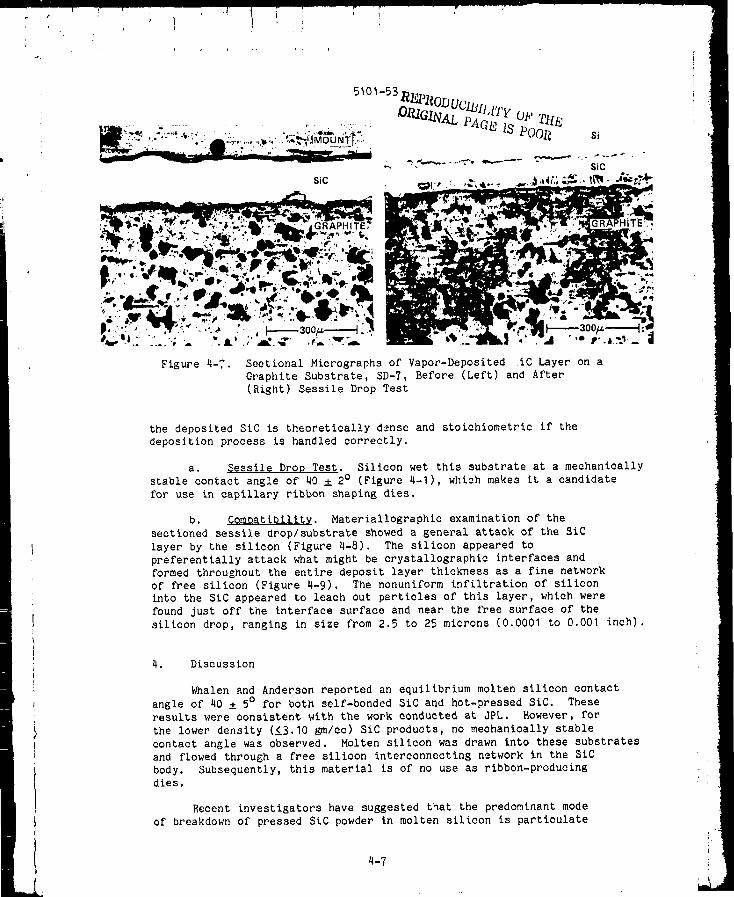
Figure 4-7. Sectional Micrographs of Vapor-Deposited IC Layer on a
Graphite Substrate, SD-7, Before (Left) and After
(Right) Sessile Drop Test
the deposited SiC is theoretically dense and stoichiometrlc if the
deposition process is handled correctly.
a. Sessile Drop Test. Silicon wet this substrate at a mechanically
stable contact angle of 40 _ 2 ° (Figure 4-I), which makes it a candidate
for use in capillary ribbon shaping dies.
b. ComDatibilltv. Materiallographic examination of the
sectioned sessile drop/substrate showed a general attack of the SiC
layer by the silicon (Figure 4-8). The silicon appeared to
preferentially attack what might be crystallographic interfaces and
formed throughout the entire deposit layer thickness as a fine network
of free silicon (Figure 4-9). The nonuniform infiltrahion of silicon
into the SiC appeared to leach out particles of this layer, which were
found just off the interface surface and near the free surface of the
silicon drop, ranging in size from 2.5 to 25 microns (0.0001 to 0.001 inch).
4. Discussion
Whalen and Anderson reported an equilibrium molten silicon contact
angle of 40 ± 5° for both self-bonded SiC and hot-pressed SiC. These
results were consistent with the work conducted at JPL. However, for
the lower density (!3.10 gm/cc) SiC products, no mechanically stable
contact angle was observed. Molten silicon was drawn into these substrates
and flowed through a free silicon interconnecting network in the SiC
body. Subsequently, this material is of no use as rlbbon-produclng
dies.
Recent investigators have suggested that the predominant mode
of breakdown of pressed SiC powder in molten silicon is particulate
4-7
5101-53
i!.
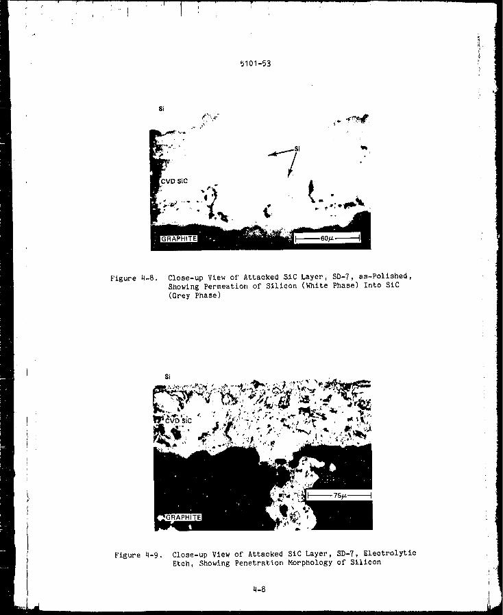
Figure 4-8. Close-up View of Attacked SiC Layer, SD-7, as-Polished,
Showing Permeation of Silicon (White Phase) Into SiC
(Grey Phase)
$i
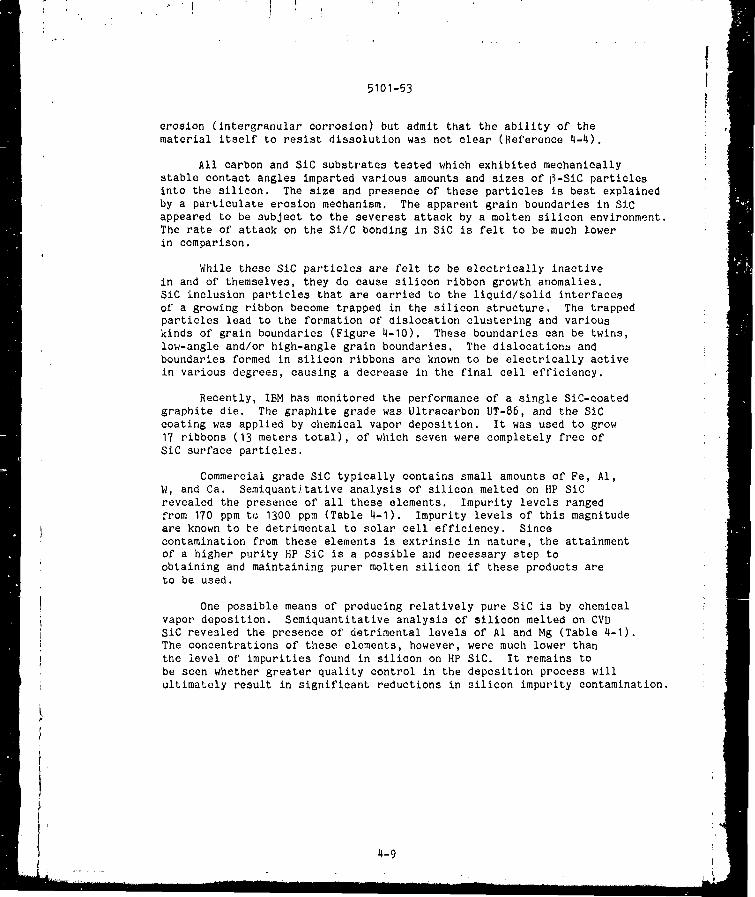
Figure 4-9. Close-up View of Attacked SiC Layer, SD-7, Electrolytic
Etch, Showing Penetration Morphology of Silicon
4-8
• i !
5101-53
erosion (intergranular corrosion) but admit that the ability of the
material itself to resist dissolution was not clear (Reference 4-4).
All carbon and SiC substrates tested which exhibited mechanically
stable contact angles imparted various amounts and sizes of i3-SiC particlesinto the silicon. The size and presence of these particles is best explained
by a particulate erosion mechanism. The apparent grain boundaries in SiC
appeared to be subject to the severest attack by a molten silicon environment.
The rate of attack on the Si/C bonding in SiC is felt to be much lowerin comparison.
While these SiC particles are felt to be electrically inactive
in and of themselves, they do cause silicon ribbon growth anomalies.SiC inclusion particles that are carried to the liquid/solid interfaces
of a growing ribbon become trapped in the silicon structure. The trapped
particles lead to the formation of dislocation clustering and variouskinds of grain boundaries (Figure 4-10). These boundaries can be twins,
low-angle and/or high-angle grain boundaries. The dislocation_ and
boundaries formed in silicon ribbons arc known to be electrically active
in various degrees, causing a decrease in the final cell efficiency.
Recently, IBM has monitored the performance of a single SiC-coated
graphite die. The graphite grade was Ultracarbon UT-86, and the SiC
coating was applied by chemical vapor deposition. It was used to grow
17 ribbons (13 meters total), of which seven were completely free of
SiC surface particles.
Commercial grade SiC typically contains small amounts of Fe, AI,
W, and Ca. Semiquant_tative analysis of silicon melted on HP SiC
revealed the presence of all these elements. Impurity levels rangedfrom 170 ppm to 1300 ppm (Table 4-I). Impurity levels of this magnitude
are known to _e detrimental to solar cell efficiency. Since
contamination from these elements is extrinsic in nature, the attainment
of a higher purity HP SiC is a possible and necessary step toobtaining and maintaining purer molten silicon if these products areto be used.
One possible means of producing relatively pure SiC is by chemical
vapor deposition. Semiquantitative analysis of silicon melted on CVDSiC revealed the presence of detrimental levels of A1 and Mg (Table 4-I).
The concentrations of these elements, however, were much lower thanthe level of impurities found in silicon on HP SiC. It remains to
be seen whether greater quality control in the deposition process will
ultimately result in significant reductions in silicon impurity contamination.
4-9

5101-53
p
SEEDINTERFACE
/
Figure 4-10. Scanning Electron Microscope Photomicrograph of SiCParticles in EFG Silicon Ribbon. Note Polr.t
and Line Defect Structure That Was Generated
B. GLASSY CARBON
Lab No. Supplier
SD-26 Tokla Electrode
Corp,
SD-27 Tokia Electrode
Corp.
SD-39 Tylan Corp.
SD-71 Fluorocarbon Co.
Density, Contact
Process gm/ee Angle
Thermal decomposition 1.53 41 m 3°
and post heat
Thermal decomposition 1,53 40 ± 2°
and post heat
Proprietary --- 44 ± 2°
(Vitregraf)
Cycllzatlon and ring 1.47 41 ± 2°
fusion polymers by
compression, then
thermal degradation(Vitrecarb)
4-10

1
aa
0
0{J
_0
0
.-3
w_J
C%
O
.r-_.PtaJ L
c. _J
_J 0
0
L•,.,I(H
a-}•_ {/)
0
!
r,oo
_o
ffl.
en
,..1
0
b..
.p
0
.(3
5101-53
(',"I
0 0 00 0
I I0
0
0
I
0 0 0
0 00 _'-
00 0
0 0O_ 0
t_
0 o
0 0
O_I
o9
"o
c_
0
c_00.,.4
0
0
00_o_0
0 0
tO
3t_
._ t_ _ t/]
_, 0 __-_ 0 _ • _ 0
0 _ ',_0 "'_ 0 _ -_•,-I _) _ 0
.M _ ._ 0 _ ,"t 0
_. 0
• 0 0 0 0 -_ 0 0 •
_) I I 0 I 0 I I ,-4
o > o _ =o _ o o
II-I I

5101-53
Glassy carbon material (SD-26 and SD-27), designated GC-20, was
manufactured by Tokla Electrode Corp., Japan, by thermal decomposition
of methyl alcohol and furfur_l alcohol (2 - C4H30 - CH2OH), with afinal heat treatment at 2000 C. This very amorphous structure had
a thickness of approximately 3.2 mm (I/8 in.). Glassy carbon material
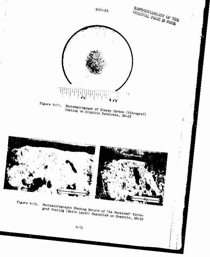
(SD-39, Vitregraf) was deposited on a graphite substrata in a proprietary
method used by the Tylan Corporation, Torrance, Calif. (Figure 4-11).The thickness of the coating was measured to be 500 - 750 microns (approximately
20 - 30 mils) and was found to be discontinuous and double layered
in several locations (Figure 4-12). Glassy carbon material (SD-71, Vitrecarb)
was produ.ed by the Fluorocarbon Company, Anaheim, Calif'., from eyclizatlon
and ring /usion polymers of the phenolaldehyde novolac and resole types,which give a high degree of crossllnking. This process results in
the turbostratic lattice rather than the graphite structure.
I. Sessile Drop Tests
Wetting properties for all glassy carbon substrates were found tobe very similar to those of silicon carbide material (8 of 40-44 °,
Figure 4-I). The degree of wetting was not observed to increase with
time as has been reported for the wetting of carbon by silicon in a
vacuum (Reference 4-I).
2. Compatibility
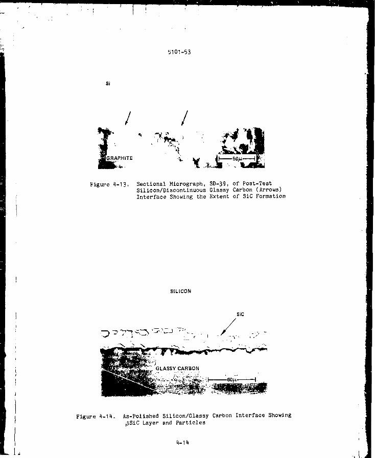
The interface reaction for all glassy carbon substrata consisted
of a _-SiC precipitation, a layer growth and dissolutionment and/orcracking. In this study, the SiC layer appeared to be adhered to the
carbon substrate, with SiC particles breaking off of the layer and
floating into the silicon matrix (Figures 4-13 and 4-14). A significant
SiC reaction layer, 20 microns (0.8 mil) thick, was observed to format a molten SiC interface after only one minute of contact time (Figure 4-15).
C. GRAPHITE (PYROLYTIC)
Density, Contact
Lab No. Supplier Process gm/cc Angle
SD-52 Union Carbide Chemical vapor 3.2 47 to 0°
deposition in 40 min
Pyrolytic graphite, SD-52, block grade HPG, was fabricated by theCarbon Product Division of Union Carbide, Cleveland, Ohio.
4-12
_a_/_ A9 _OO_ _
, _II ,_ i'l'!ilr_ ,,
Figure 4-11, Photomacrograph of Glassy Carbon (Vitregraf)Coating on Graphite Substrate, SD-39
Figure 4-12. Photomicrographs Showing Natuee of "As Received" Vitre-
graf Coating (White Layer) Deposited on Graphite, SD-39
4-13
!
5101-53
$i
/ /
Figure 4-13, Sectional Micrograph, SD-39, of Post-Test
Silicon/Discontinuous Glassy Carbon (Arrows)
Interface Showing the Extent of SiC Formation
SILICON
SiC
_:2 _GLASSY CARBON
Figure 4-14. As-Polished Silicon/Glassy Carbon Interface Showing
_SIC Layer and Particles
4-14

! !
5101-53l".l'iI'_i(_i l_ P i .;,, .,! ILJb.;
_u,;( " "_' I""1;;, l:.; PUUJt,
SILICON
Figure 4-15. As-Polished Sillcon/Glassy Carbon Interface After
One Minute Contact With Molten Silicon
I. Sessile Drop Test
Molten silicon was observed to wet the graphite surface at
approximately 47 ° after the initial 15-min contact period. Photographic
results indicated the rate at which the silicon was aosorbed into the
substrate (2 x 10⁻⁴ gm/sec). The contact angle decreased as silicon was
absorbed (Figure 4-I). It is important to note that the decrease in the
contact angle from 47 to 0 ° in 40 min was not due to spreading. Essentially,
all free sllic_n was being absorbed and converted to SiC. No free silicon
was ±eft on the test surface (Figure 4-16). Weak planar bonds of the
pyrolytic graphite were attacked by the molten silicon, resulting in an
exfoliatlon or delaminatlon phenomenon (Figure 4-17). Growth of the SiC
zone resulted in stresses which disrupted the deposited graphite layers.
2. Discussion (Si and C)
When molten $i contacts C, }3-SIC is formed at the interface
(Reference 4-5). Whalen and Anderson (Reference 4-I) state that there is
abundant evidence of reaction and in some cases infi].tration of the
carbon by liquid silicon. Chang and Siekhaus (Reference 4-6) observed
very fast diffusion rates of silicon and carbon into each other with the
formation of SiC. They also proposed a diffusion mechanism whereby
silicon atoms first form a carbide layer wlth the surface carbon atoms,
followed by repeated cracking of the carbon lattice and diffusion of silicon
4-15

5101-53
_, L_4,,I•
:L_:_,_:i-.•,:__I
II
ttttlltil I..!NC HES (lOths) I
Figure 4-16. Post-Ses_lle Drop
Test Surface, SD-52
Figure 4-17. Section Taken Through Delaminated Area, Which Also
Shows SiC Formation, as-P31ished, SD--52
4-16

5101-53
through the carbide layers. Growth of the SiC layer causes distortion ofthe structure, which is relieved by cracking. The interface reactions
for St and C observed in this study were qualitatively explained by this
mechanism. In general, it appeared that the formation and subsequent
cracking of SiC at the molten silicon/glassy carbon interface occurred
more rapidly than the surface dissolution or breakdown of hot-pressedSiC in contact with molten silicon. IBM (Reference 4-7), however, has
stated that the much greater SiC particle pickup from graphite (dies)
than from SIC-coated graphite dies is not thought to be related to a
difference in solubility. The difference was accounted for by the natureof the nucleation sites for crystallization of excess SiC from the carbon-
saturated liquid silicon at the SiC die top. If the SiC die materialpromotes better adherence of SiC grown from solution than does graphite,
then less free particulate SiC would be available in the meniscus region
for incorporation in the growing ribbon. This concept has neither been
verified nor disproved as yet.
Carbon which is incorporated substitutionally into silicon leads to
lattice constriction. A possible result of this lattice constriction is
stress-relief twinning. Twinning occurs profusely in CAST ribbons grown
with carbon dies; no way to eliminate it is presently known (Reference 4-8).
To date, high-denslty graphite (poco grade) has been used for mostsilicon ribbon growth. It is not, however, completely nonreactive
(Figure 4-18). Good crystallographic quality has been achieved onsmall, carefully grown ribbon segments (References 4-9 and 4-10), but
the structure of large ribbons grown fast is full of all sorts of
planar, llne and point defects.
,.. ,;_ _ '_" SiC
.... --/'. " .v ., • _-'_'_i:........... /... ,,,. •• / • :.... .- .. ' - .','.:._;'!i:_;._<.' ,
_ .,r,,,_J"0_' '_"_ TwI.NS_/: " . " "" " ;;'_::'.];__i'__:'; ! "
". , _ ' _ -'-:-----_---_-_-2t.'_-_" -'_:,.""'E"._-.._?-,.,,,__-_--...-..... _,,,,--,_- .....-'---<'1.._" _,;-,.
-._.'.',_{__C_';- ........", -:-............:,.
..._. . . _,__.-:;'.;,_,, -,, !/ .__'
• .' I :.; ._:;i "_ . . ...-, , - t---_2OO/._-------t
Figure 4-18. Surface of Silicon Ribbon Grown by EFG Method Using
Poeo Graphite Die. Note Point and Line Defects
4-17
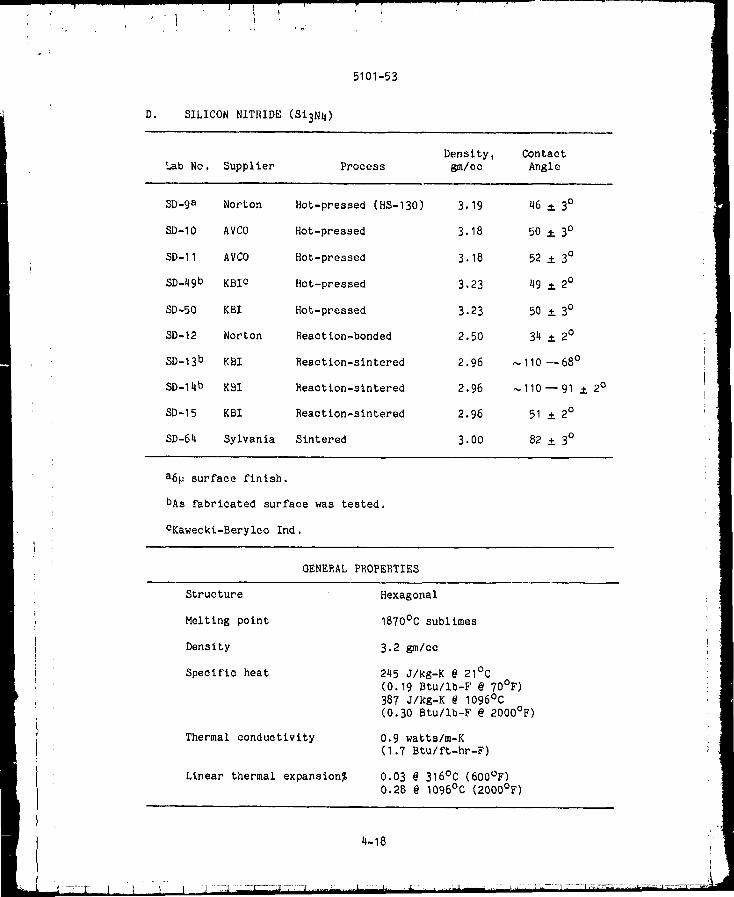
Do SILICON NITRIDE (Si3N4)
5101-53
Lab No. Supplier Process
Density,gm/cc
Contact
Angle
SD-9 a Norton Hot-pressed (HS-130)
SD-IO AVCO Hot-pressed
SD-11 AVCO Hot-pressed
SD-49 b KBI c Hot-pressed
SD-50 KBI Hot-pressed
SD-12 Norton Reaction-bonded
SD-13 b KBI Reaction-sintered
SD-14b KBI Reaction-sintered
SD-15 KBI Reaction-sintered
SD-64 Sylvania Sintered
3.19
3.18
3.18
3.23
3.23
2.50
2.96
2.96
2.96
3.00
46 ± 3°
50 ± 3°
52 ± 3°
49 _ 2°
50 _ 3°
34 ± 20
110_68 °
110_91 ± 2°
51 ± 2°
82 ± 3 °
a6_ surface finish.
hAs fabricated surface was tested.
CKawecki-Berylco Ind.
GENERAL PROPERTIES
HexagonalStructure
Melting point
Density
Specific heat
Thermal conductivity
Linear thermal expansion%
1870°C sublimes
3.2 gin/co
245 J/kg-K @ 21°C
(0.19 Btu/ib-F @ 70°F)
387 J/kg-K @ I096°C(0.30 Btu/ib-F @ 2000OF)
0.9 watts/m-K(1.7 Btu/ft-hr-F)
0.03 @ 316°C (600°F)
0.2B @ I096°C (2000°F)
4-18

T:Ibl¢." Jl-.!. 'l'ypteal Clu,_iII:d, vy Dat.a _t._Nll l'voduot,:_ (wt $)
E 1 em oll t
St
N
AI
Ca
N:l
K
O,t
NoI'to¢1 H._- I ._0
( }{et'ez'onec Jl- I .] ) Not'Ion ".g'_O" KI_I
bO. t!
I ._'I. 0
O. 5 0.. Ii O, 8
0.1 - 0,2 0.2 0.0
0.003 - 0.008 0.05 0,!,
0.00_! - 0.01 ___
O.OOll - 0.008 --.
0.._ - 0._I ---
O, 5
1. IIot i'l'e,_aed
-'_t_Nll powder t_ eomtt_onLy mixed 'aiLh _._tl addtLive and hot.-pt'es_edbeLNeen "1000 - 18!_0°0 at. ,IppLted pt'e_tttlt'ot_ le,-_ Lhatl _tl.¢_ x 10 5 N/t1_ 2
(_._000 pat) (Bet'_l'ol_ee._ 4-11, 12, 1.{) ill tt_tt'ot_etl of itle_'L gas
atmo_phet'e_. The t'e._ult.ant p_'oduot l._ a maxtmum-don._tt.y, ht_h-st._,en_,,t,l_,
beta-phase SI._Nll ('l'abke II-/').
Sevt'_'aI lnvo,_t t_atot,-_ ( Ret'et'enees )1-1!_ tht'ou_h 11- 18) have ,_tA_d ted
Lhe slt_tet'ing effeet._ of I'_0 tn tl_e hot-pvot_t_tng of S_NII, and rillt'epot't, ed obt¢_tlttlg Aft b_t,_O - SL0_ [_,ltlid Rt'_tn bO_tt_d;_l'y ph;_o. N. b]t tomo
(t_et'et'enee 4-'q1 t'ut't.het' tnvest.ig;xt.ed the stt+t.et'_n_-, of St+Nil x+i.t.h !+$ _.;0 and
:m_'veyed t:tle :_ttltet'it_t', et't'eet:8 of ot, hel' add_t.tve8 (5$ wt). '['he vat'.tou_
nddit.[ve:_ ;llld dolll_[t.y v,ll.tl¢'8 ob[:l_llod ¢lfl.or l'_bv.to;it.to[l nl'e 8ho_n .(tl
'k':_ble li-._, l_, i:_ imlx_]'t, an_ t.o note t.l_at, litLle is known nbout the
_\_t't i,,ulat' eft'eeL of mo_teu _ikteo_ on such den:_it'lention addttLvo._
a:_ notad fix t.hi_ table. I{ov_evet'_ dtst_oLul Lou of b_,; t't'om hot-pt'e_sed
SLjNI I h;_s been ob_et'w_d in t:l_t,_ pvograt_ Atld is dtseu:-',_od tater'.
5101-53
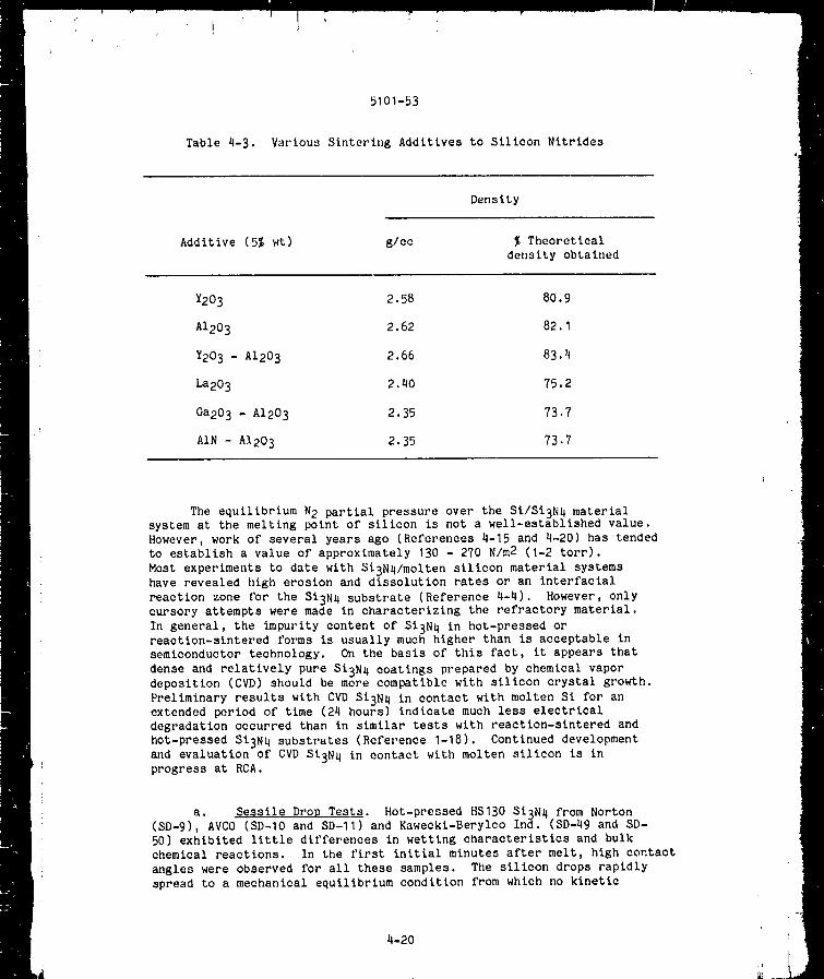
Table 4-3. Various Sinterlng Additives to Silicon Nitrldes
Density
Additive (5% wt) g/cc % Theoreticaldensity obtained
¥203 2.58 80.9
AI203 2.62 82.1
Y203 - AI203 2.66 83.4
La203 2.40 75.2
Ga203 - AI203 2.35 73.7
AIN - AI203 2.35 73.7
The equilibrium N2 partial pressure over the SI/SI3N 4 materialsystem at the melting point of silicon is not a well-establlshed value.However, work of several years ago (References 4-15 and 4-20) has tended
to establish a value of approximately 130 - 270 N/m2 (I-2 tort).
Most experiments to date with Si3N4/molten silicon material systemshave revealed high erosion and dissolution rates or an Interfaclal
reaction zone for the SI3N 4 substrate (Reference 4-4). However, onlycursory attempts were made in characterizing the refractory material.
In general, the impurity content of SI3N 4 in hot-pressed orreaction-slntered forms is usually much higher than is acceptable insemiconductor technology. On the basis of this fact, it appears that
dense and relatively pure SI3N 4 coatings prepared by chemical vapordeposition (CVD) should be more compatible with silicon crystal growth.
Preliminary results with CVD Si3N 4 in contact with molten Si for anextended period of time (24 hours) indicate much less electrical
degradation occurred than in similar tests with reaction-slntered and
hot-pressed Si3N 4 substrates (Reference 1-18). Continued development
and evaluation of CVD Si3N 4 in contact with molten silicon is inprogress at RCA.
a. Sessile Drop Tests. Hot-pressed HS130 SI3N 4 from Norton(SD-9), AVCO (SD-IO and SD-11) and Kawecki-Berylco In8. (SD-49 and SD-50) exhibited little differences in wetting characteristics and bulk
chemical reactions. In the first initial minutes after melt, high contact
angles were observed for all these samples. The silicon drops rapidly
spread to a mechanical equilibrium condition from which no kinetic
4-20
5101-53
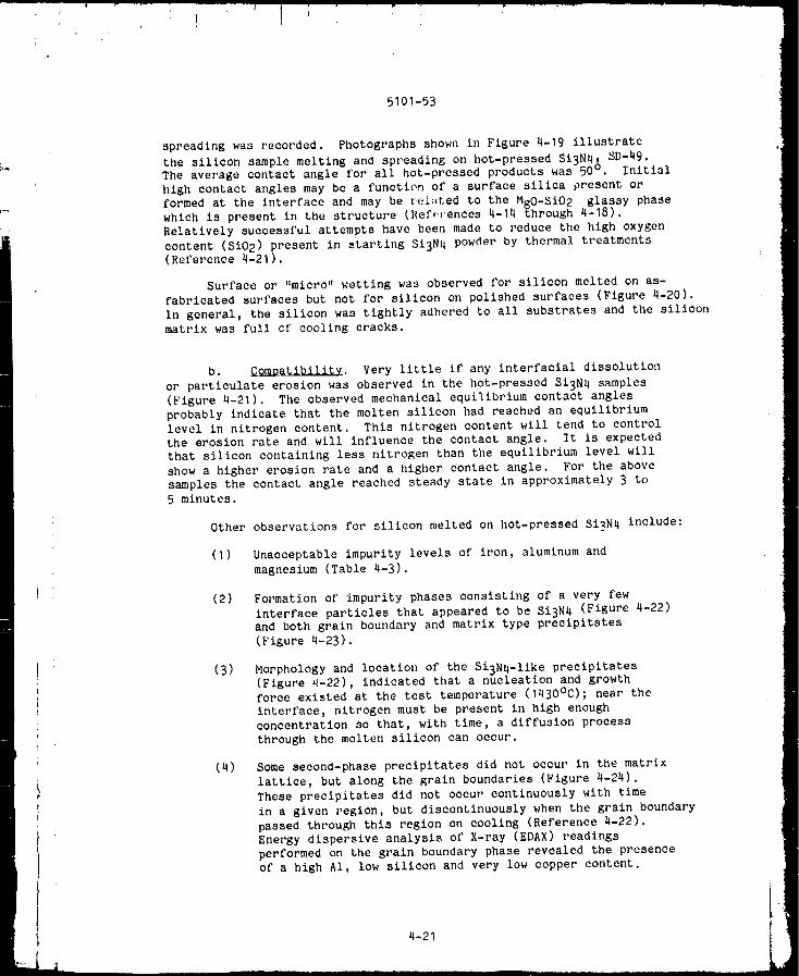
spreadingwasrecorded. Photographsshownin Figure4-19illustratethe silicon samplemeltingandspreadingon hot-pressedSi3N4,SD-49.Theaveragecontactanglefor all hot-pressedproductswas50° . Initialhighcontactanglesmaybea function of a surfacesilica presentorformedat the interface andmaybe rel:,ted to the MgO-SiO2glassyphasewhichis presentin the structure (Ref,'Lenccs4-14through4-18).Relatively successfulattemptshavebeenmadeto reducethe highoxygencontent(SIC2)presentin starting Si3N4powderby thermaltreatments(Reference4-21).
Surfaceor "micro" wetting was observed for silicon melted on as-fabricated surfaces but not for silicon on polished surfaces (Figure 4-20).
In general, the silicon was tightly adhered to all substrates and the siliconmatrix was full of cooling cracks.
b. _9_nl_gtlbilitv. Very little if any interfacial dissolution
or particulate erosion was observed in the hot-pressed SI3N 4 samples(Figure 4-21). The observed mechanical equilibrium contact angles
probably indicate that the molten silicon had reached an equilibrium
level in nitrogen content. This nitrogen content will tend to controlthe erosion rate and will influence the contact angle. It is expected
that silicon containing less nitrogen than the equilibrium level will
show a higher erosion rate and a higher contact angle. For the abovesamples the contact angle reached steady state in approximately 3 to
5 minutes.
Other observations for silicon melted on hot-pressed Si3N 4 include:
(I) Unacceptable impurity levels of iron, aluminum and
magnesium (Table 4-3).
(2) Formation of impurity phases consisting of a very few
interface particles that appeared to be Si3N4 (Figure 4-22)and both grain boundary and matrix type precipitates
(Figure 4-23).
(3) Morphology and location of the Si3N4-1ike precipitates(Figure 4-22), indicated that a nucleation and growthforce existed at the test temperature (1430°C); near the
interface, nitrogen must be present in high enoughconcentration so that, with time, a diffusion process
through the molten silicon can occur.
(4) Some second-phase precipitates did not occur in the matrix
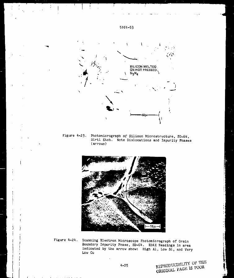
lattice, but along the grain boundaries (Figure 4-24).
These precipitates did not occur continuously with time
in a given region, but discontinuously when the grain boundary
passed through this region on cooling (Reference 4-22).Energy dispersive analysis of X-ray (EDAX) readings
performed on the grain boundary phase revealed the presence
of a high AI, low silicon and very low copper content.
4-21
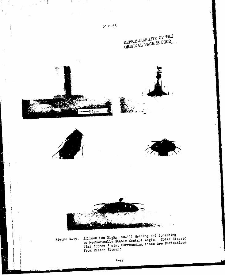
5101-53
[L_,3_oDUCt_[bITyOF T_
Figure 4-19, Silicon (on Si3N4, SD-49) Melting and Spreadingto Mechanically Stable Contact Angle. Total ElapsedTime Approx 3 min; Surrounding Lines APe ReflectionsFrom Heater Element
4-22
II II1"ill ........... ,::,_................ " III I I iJ " '__'_"i1[lll'[I]il.........."_ ' I" II III "_

5101-53RI,Sp[{oI}UL'I!_I!,[TY 01,' 'fill,;
SILICON
!r-; , _-- ",] - ,
Figure 4-20. Silicon Sessile Drop on as-Fabricated Test Surface,SD-49 (Left), and on a 15_ Surface Finish SD-50,
(Right). Note Microwetting Around Sessile Drop onthe Left
SILICON
HOT PRESSED SI3N4
1_120/J.._]
Figure 4-21. Photomicrograph of Sillcon/Si3N 4 Interface,SD-50, as-Pollshed
4-23
5101-53
i'
Si3N4
$i
Figure 4-22,Si3N 4 Appearing Particles at SI/Si3N 4 Interfaceand Slight Silicon Permeation Into Substrate, SD-9,
Hot-Pressed Si3N4,
4-24
J
5101-53
L_. _
!\
i \
SILICON"MELTED,
ON HOT PRESSED,_Si3N4
Ir
="
' F
".'_%
\
Figure 4-23. Photomicrograph of Silicon Microstructure, SD-64,Sirtl Etch. Note Dislocations and Impurity Phases
(arrows)
Figure 4-24. Scanning Electron Microscope Photomicrograph of Grain
Boundary Impurity Phase, SD-64. EDAX Readings in area
indicated by the arrow show: Nigh AI, Low Si, and VeryLow Cu
4-25 I%EPI%OI)UCIBILTfN OF T_IE
OI_,IGINAL PAGE IS 9OO1%

t
5101-53
2. Reaetion-Sinterlng/Bonding
In reaction-sintering/bonding, the required shape is made from
compacted silicon powder nltrided in nitrogen in the range of 1400°C.
This gives a product of mixed n and 13 silicon nitride with about 25%
porosity. After a product is compacted, the original dimension
remains essentially unchanged during nitridlng, which allows for complex
finish shapes. Reaetion-sintered Si3N 4 (SD-13, SD-14, and SD-15) was
made by Kawecky-Berylco Industries.
a. Sessile DEop Tests. Samples SD-13 and SD-14 were tested
using the as-fabricated surface. These samples showed (I) very high
initial wetting angles during the first minutes of melt (_110 ° initially),
and (2) a spreading contact angle, which for SD-14 appeared to stabilize
at 91 ± 20 and for SD-13 decreased to 68 ° in approximately 35 min of
melt time. Reactlon-sintered sample SD-15, 15 p test surface finish,
exhibited essentially the same wetting kinetics and final contact angle
as hot-pressed SI3N 4 (51°).
Oilier
(I)
(2)
observations for silicon melted on RS Si3N 4 Included:
Silicon was tenaciously bonded to the SI3N4, which caused
the solidifying silicon to crack. This is because of
differing thermal expanslon/contrsction characteristics
(Figure 4-25).
Silicon wicked along the test surface for unpolished sub-
strates, indicating a possible surface "micro" wetting
phenomenon (Figure 4-26), but did not for polished substrate.
b. Compatibility. The high initial contact angle observed
on both hot-pressed and reaction-sintered Si3N 4 is believed to be caused
by a thin layer of silica which is present at the interface. The source
may be SiC 2 on initial Si3N 4 powder, producing an influence on initial
wetting behavior.
Sample SD-14 retained a high contact angle (91 ° ) throughout the total
35-min melt time. The sillcon/Si3N 4 interface of this sample was observed
in the scanning electron microscope. SEM photomicrographs revealed
the presence of a thin interface layer (Figure 4-27). Energy-dispersive
analysis of X-rays (EDAX) which were performed on this layer and surrounding
areas revealed three separate and distinct silicon counts. The highest
count was on the Si matrix; the lowest count was on the Si3N 4 matrix.
The thin interface layer is believed to be a silicon oxide. Actual
phase det(.rmination, however, was not accomplished.
Silicon melted on reaction-sintered Si3N 4 substrates revealed (I) in
general, the lack of any interfaclal reaction zone, (2) very high detri-
mental impurity levels of iron, aluminum, manganese and calcium (Table 4-3),
(3) a greater quantity of precipitates in the silicon than for silicon on
hot-pressed Si3N 4 products, and (4) a larger size and quantity of Si3N 4-
appearing particles at the interface than with hot-pressed SI3N4.
4-26

5101-53
SLCON i " _':' " _ii' " "
.,r,_7 _'_,_ .... _'"
•o• _:' ' ,, _.._.._REACTION SINTERE Si3N4
, "(_'C_':-_.j._,,:,._._, .._W#.'_"
F'_0.5 crn_ _- "';+" -,.' "' _' ' ',+"7"_'+ ' '_'.
%
Figure 4-25. Photomacrograph of Sectioned Sessile Drop, SD-15,Showing Cracks in Silicon. Irregular Sessile Drop
Shape is Due to Expansion Characteristic ofSolidifying Silicon
3. Discussion (Si On Si3N 4)
Single-phase, dense, hot-pressed silicon nitride is impossible to
obtain by present production methods. However, single-phase material
may not be necessary. For example, chemically pure, two-phase c and
Si3N 4 may prove a feasible substrate. The problem with present-day
hot-pressed Si3N _ is its impurity content. The presence of impurity
elements in Si3N4, i.e., iron, aluminum, calcium and magnesium in the
SisN4, will result in detrimental contamination of the _ilicon, whichsubsequently results in an electrically deficient solar cell. Toattack and solve this problem will require greater quality control in
maintaining starting powder purity. One way of almost entirely
eliminating the extrinsic contamination problem with Si3N 4 is the useof a SI3N 4 CVD film. Table 4-4 shows the relative impurity levels for
various Si3N 4 products.
'_ '".... _[!('l_:l_ I I'V ._i.' i'i.l/,,_
OI_IGI_'AI,I)AG!:i:i l_()(}R
4-27

Figure 4-26.
I i
5101-53
Photomicrograph of Interface, SD-14, Near Edge
of Sessile Drop. Note the Presence of Free
Silicon Beyond the Edge of the Silicon Drop
(Microwettlng)
Figure 4-27. Scanning Electron Microscope Photomicrograph of
Sillcon/RS SI3N 4 Interface SD-14, Showing
Thin Layer of Intermediate St Content (Arrow)
4-28
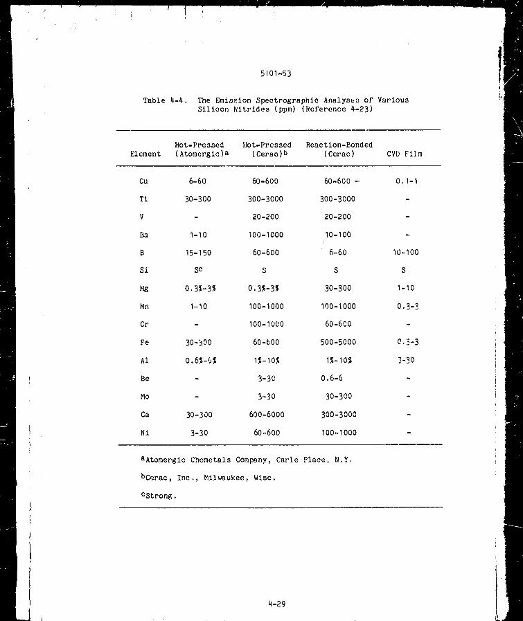
Table 4-4.
5101-53
The Emission Spectrographic Analysec of VariousSilicon Nitrides (ppm) (Reference 4-23)
Hot-Pressed Hot-Pressed Reactlon-Bonded
Element (Atomergic)a (Cerac)b (Cerac) CVD Fi]m
Cu 6-60 60-600 60-600 - 0.1-I
Ti 30-300 300-3000 300-3000 -
V - 20-200 20-200 -
Ba 1-10 100-1000 10-100 -
B 15-150 60-600 6-60 10-100
Si se S S S
Mg 0.3%-3% 0.3%-3% 30-300 1-10
Mn 1-10 100-1000 100-1000 0.3-3
Cr - 100-1000 60-600
Fe 30-300 60-600 500-5000 0.3-3
AI 0.6%-6% I%-I0% I%-I0% 3-30
Be - 3-30 0.6-6
Mo - 3-30 30-300
Ca 30-300 600-6000 300-3000 -
Ni 3-30 60-600 100-1000 -
aAtomerglc Chemetals Company, Carle Place, N.Y.
bCerac, Inc., Milwaukee, Wisc.
CStrong.
4-29
1
5101-53
E. SILICON OXYNITRIDE (Si2ON2)
Density, Contact
Lab No. Supplier Process gm/cc Angle
SD-35 Norton Sintered (SiOXYN) 2._6 115 ± 3°
SD-37 a Norton Sintered (SiOXYN) 2.46 117 ± 2 °
aAs-fabricated surface tested.
Commercial grade multi-phase silicon oxynitride, SD 35a and 35b,
was synthesized by Norton Industrial Ceramics Division by reacting
mixtures of silicon and silica with nitrogen at elevated temperatures.
SiOXYN shapes are self-bonded and are formed in the desired shape before
firing. Fully reacted SiOXYN powder alone, when compacted and sintered,
does not exhibit good strength properties;-however, the addltion of
other binders will help, but is likely to limit the product's performance
capabilities. Typical contents of SiOXYN are 75 to 90% Si2ON2, I to
7% eristobalite, 0.7% iron, 0.4% calcium, and the balance silicon nitride.
I . Sessile Drop Test
(I) Beth samples exhibited equilibrium wetting at approximately
116 ° .
(2) There were no apparent differences in wetting characteristics
between the as-fabricated and polished surface.
(3) Molten silicon wicked along the SiOXYN surface all
around the sessile drop ("micro" wetting) (Figure 4-28).
2. Compatibility
(I) An interface reaction zone approximately .08 mm (3 mils)
thick was formed (Figure 4-28).
(2) Silicon penetrated the substance in the center portion
of the int,erface area
(3) Surface "microwetting" was observed (area B, Figure 4-28).
(4) An oxide type film was observed on portions of tne molten
silicon drop surface.
4-30

, C
v
, ;I '
1 ; r, e
5101-53 REPRODUCIi{ILLTY OF TIib;ORIGINAL PACI4 IS PO<)[{
Figure 4-28. Silicon Oxynitride, Photomacrograph (Left) of SectionedSample Showing, A - Unreacted Test Surface, B - Reacted
Surface (Silicon Wicked in) and C - Silicon Drop. Photo-
micrograph (Right) of Interfacial Reaction Zone
3. Discussion
To date, single phase SI20N 2 has not been known to be fabricatedby hot pressing or reaction bonding. There is evidence of pyrolytically
produced SixOyN films (Refs. 1-18, 4-11, 4-2_). Complete documentationof the resulting structure was not readily available. Preliminarytests with CVD layers of silicon oxynitrtde in contact with molten
Si have been encouraging (Ref. 1-18). It is expected that the physical
properties of an amorphous silicon oxynitride film in contact with
molten Si will be strongly dependent on the oxygen concentration.
F. SILICON-ALUMINUM-OXYGEN-NITROGEN (SIALONS)
Phase (all
material was Density,
Lab No. Supplier hot pressed) gm/cc Contact Angle
SD-28 JP5 X2, two phasea 3.33 (65-80°62 °) ± 3°
SD-29 JP5 6' 3.09 (55-48 °) ± 3°
SD-30 JP5 D' 3.09 54 ± 3°
SD-58 JPL #', SiO 2 + AIN 3.23 44 ± 2°
SD-57 JPL 15R, AIN + 3.37 91-52 °
Si3N 4 + A1203
4-31

J
1 I '
5101-53
F. SILICON-ALUMINUM-OXYGEN-NITROGEN (SIALONS) (Continued)
Phase (all
material was Density,
Lab No. Supplier hot pressed) gm/cc Contact Angle
SD-59 JPL 154, high Et3N _ 2.54 112"59 °-1% MgO
SD-62 JPL 15_, w/1% B203 3.06 Not tested
SD-63 JPL 15R, AIN +SiO 2 3.10 Not tested
SD-60 JPL 8H, polyphase 3.37 90-57 °
SD-61 JPL 8H, polyphase 3.37 62-52 °
I% _o
SD-65 JPL Polyphase Ba 3.30 84_53 °
SD-66 JPL Polyphase Aa 3.34 80-51 °
aSee Figure 4-29
All hot-pressed slalon samples used in sessile drop tests were fabricatedat JPL. (Samples were provided by Wayne Phillips). No binder additives were
used except for SD-59, SD-61, and SD-62, so that, at temperature, all denslfication
occurred by reactlon-bondlng. No liquid phase sintering can be expected
at the fabrication temperatures used. _rther fabrication information notincluded in the above table is given in Table 5.
Jack (Reference 4-25) has studied sialons and related nitrogen
ceramics and has reported much useful information. The results of hot-
pressing appropriate mixtures of SigN4, AIN, A1203, Si02 and SI2N _at high temperatures (usually 1750°_, but ranged from 1550 - 2000_C)
in a graphite die are shown in Figure 4-29. At best, this dlag_am
can be considered idealized behavior and does not necessarily represent
thermodynamic equilibrium.
The phase "X" was reported by Oyama and Kamigaito (Reference 4-26)
to have the composition 3A1203 • Si3N4. However, work by Jack indi-cates that the X-phase slalon composition, SIAI02N (Reference 4-27),
is more rich in AI203 (Reference 4-25), but that further work isneeded in this area. There is the suggestion that describing the
X-phase as a "nltrogen-mulllte" is not misleading. Attempts have
been made at the United Technologies Research Center to prepare
Si6.xAlxOxN8_x solid solution ceramics by reacting X-phase liquidand a complementary slalon composition and subsequently homogenizing
them to a single phase (Reference 4-28).
4-32
.,j,'
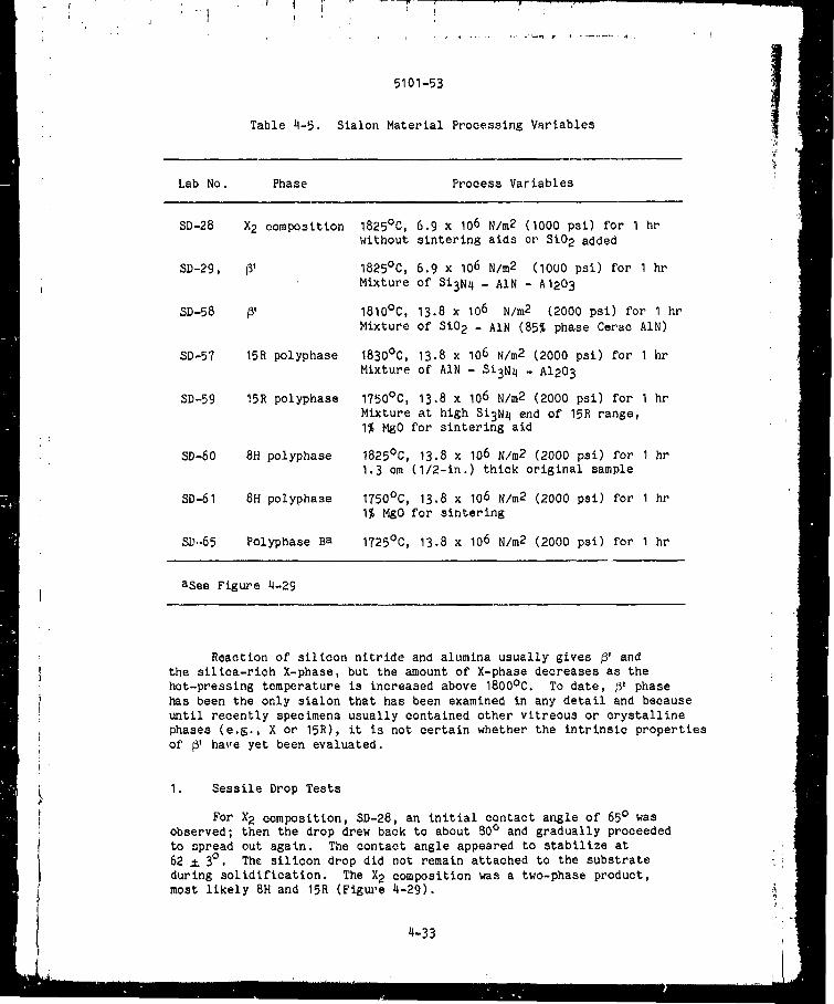
- I i
s, i
5101-53
Table 4-5. Sialon Material Processing Variables
Lab No. Phase Process Variables
SD-28 X 2 composition 1825°C, 6.9 x 10⁶ N/m 2 (1000 psi) for I hr
without sinterlng aids or SiO 2 added
SD-29, _' 1825°C, 6.9 x 10⁶ N/m 2 (1000 psi) for I hr
Mixture of SI3N 4 . AIN - A1203
13.8 x 10⁶ N/m 2 (2000 psi) for I hr
of Si02 - AIN (85% phase Cerac AIN)
13.8 x 10⁶ N/m2 (2000 psi) for I hr
of AIN - Si3N 4 . AI203
13.8 x 10⁶ N/m2 (2000 psi) for I hr
at high St3N 4 end of 15R range,
for sintering aid
13.8 x 10⁶ N/m2 (2000 psi) for I hr
(1/2-1n.) thick original sample
13.8 x 10⁶ N/m2 (2000 psi) for I hr
for sintering
13.8 x 10⁶ N/m2 (2000 psi) for I hr
SD-58 _' 1810°C,
Mixture
SD-57 15R polyphase 1830°C,
Mixture
SD-59 15R polyphase 1750°C,
Mixture
i% MgO
SD-60 8H polyphase 1825°C,
1.3 cm
SD-61 8H polyphase 1750°C,
i% MaC
SD.-65 Polyphase Ba 1725Oc,
aSee Figure 4-29
Reaction of silicon nitride and alumina usually gives _' and
the sillca-rich X-phase, but the amount of X-phase decreases as the
hot-presslng temperature is increased above 1800°C. To date, _' phase
has been the only sialon that has been examined in any detail and because
until recently specimens usually contained other vitreous or crystalline
phases (e.g., X or 15R), it is not certain whether the intrinsic properties
of _' have yet been evaluated.
I
I. Sessile Drop Tests
For X 2 composition, SD-28, an initial contact angle of 65 ° was
observed; then the drop drew back to about 80 ° and gradually proceeded
to spread out again. The contact angle appeared to stabilize at
62 ± 3°. Th£ silicon drop did not remain attached to the substrate
during soltdtficatlon. The X2 composition was a two-phase product,
most likely 8H and 15R (Figure 4-29).
4-33
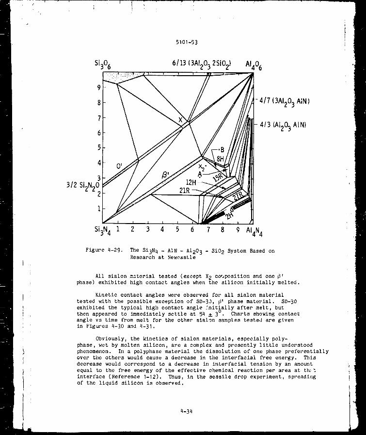
51Ol-53
Si306 6/13(3A12032SiC2) AI406
9
8
7
6
5
4
3
3/2 Si2N2(
4/7 (3AI203 AIN)
4/3 (AI203 AIN)
Si3N4 1
Figure 4-29.
2 3 4 5 6 7 8 9 AI4N4
The Si3N 4 - AIN -.AI203 -SiO 2 System Based onResearch at Newcastle
AII slalon material tested (except X2 co_position and one _'phase) exhibited high contact angles when the silicon initially melted.
Kinetic contact angles were observed for all slalon material
teated with the possible exception of SD-3J, _' phase material. SD-30exhibited the typical high contact angle Lnltially after melt, butthen appeared to immediately settle at 54 _ 3° • Charts showing contact
angle vs time from melt for the other sialon samples tested are given
in Figures 4-30 and 4-31.
Obviously, the kinetics of sialon materials, especially poly-
phase, wet by molten silicon, are a compIex and presently little understood
phenomenon. In a polyphase material the dissolution of one phase preferentially
over the others would cause a deerease in the interfacial free energy. Thisdecrease would correspond to a decrease in interfacial tension by an amount
equal to the free energy of the effective chemical reaction per area at th_
interface (Reference 1-12). Thus, in the sessile drop experiment, spreading
of the liquid silicon is observed.
4-34
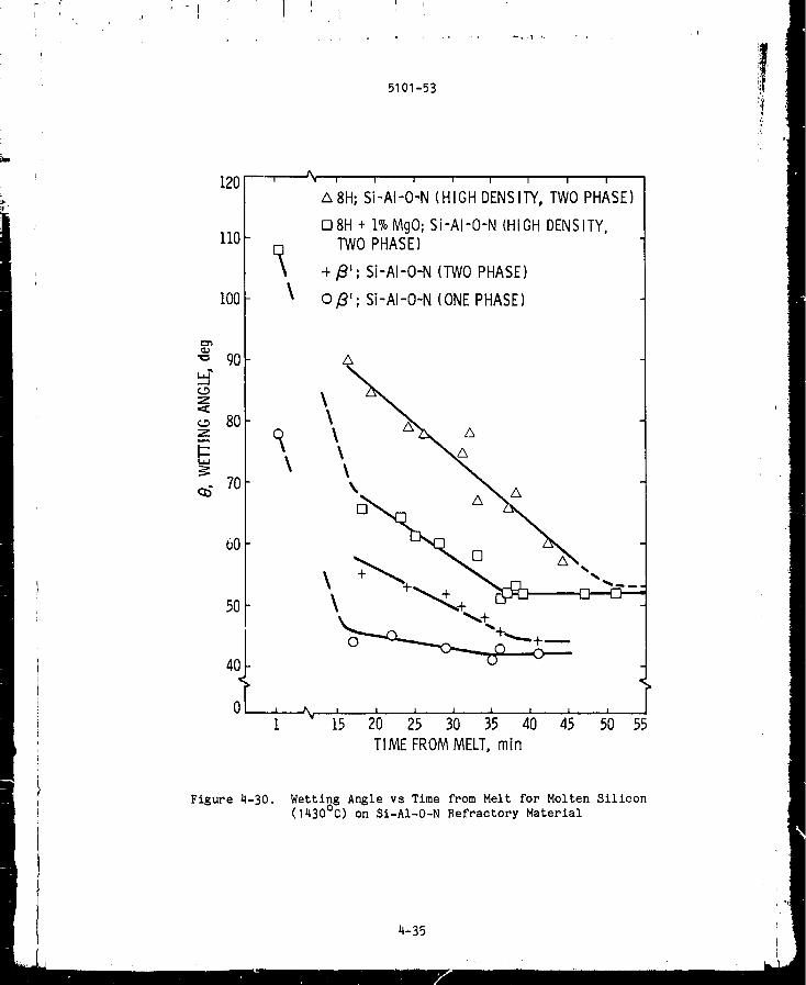
-t
5101-53
i:iA
_DZ
Zm
E
120
110
100
I
\
9O
8O
\70
60
50
1
I 1 I I I I I I
A 8H; Si'AI-O'N (HIGH DENSITY, TWO PHASE)
IZ]8H + 1"/oMgO; Si-AI-O-N (HIGH DENSITY,TWO PHASE)
+ ,8'; Si-AI-O-N (TWO PHASE)
O/_'; Si-AI-O'N (ONE PHASE)
A
\
t_ I I I I I I I I
15 20 25 30 35 40 45 50 55
TIME FROM MELT, rain
Figure 4-30. Wetting Angle vs Time from Melt for Molten Silicon(1430°C) on Si-AI-O-N Refractory Material
4-35
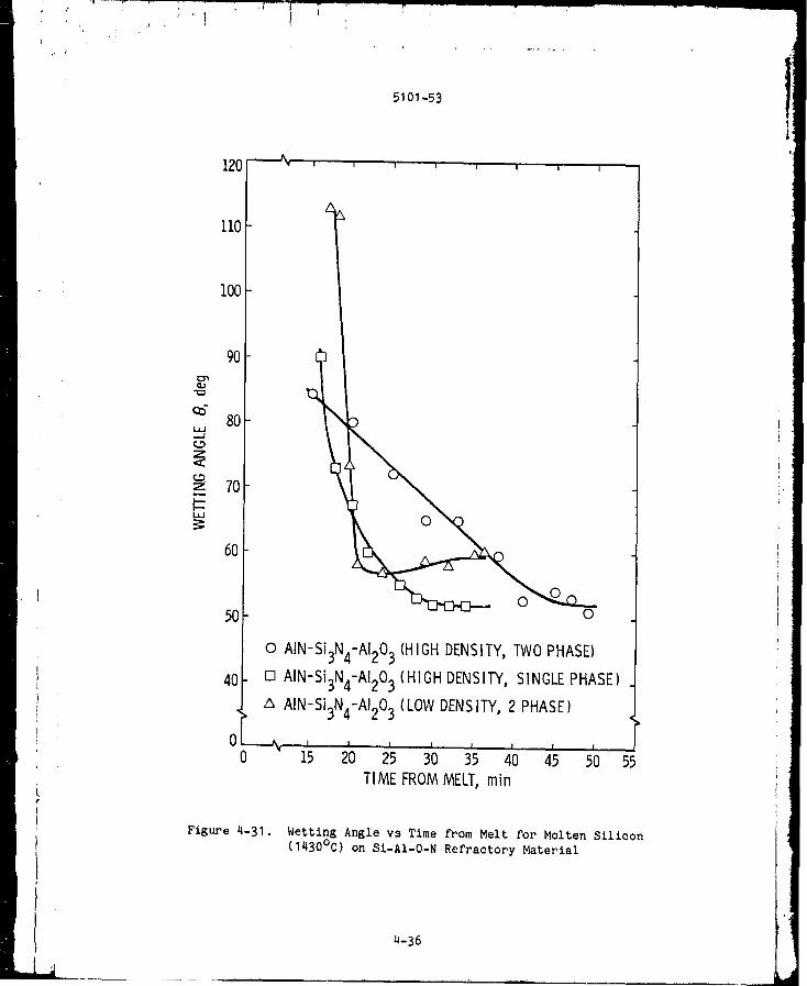
5101-53
I.l.J,-=1
Z
Z
ILl
120
110
100
90
80
70
60
50
40
I I I i i i I I
o
O AIN-Si3N4-AI203(HIGH DENSITY, TWO PHASE)
[] AIN-Si3N4-AI203(HIGH DENSITY, SINGLE PHASE)
L- Z_ AIN-Si3N4-AI203 (LOW DENS,ITY,2.PHASE) I0 _,, , , , , , , ,
0 15 20 25 30 35 40 45 50 55
TIME FROM MELT, rain
Figure 4-31. Wetting Angle vs Time from Melt for Molten Silicon
(1430°C) on Si-AI-O-N Refractory Material
4-36

5101-53
2. Compatibility
For X2 composition, SD-28, the presence of an additional phase(light gray), besides the two original substrates phases (medium grayand dark brown), was found near the interface zone as observed in
reflected light. Also, narrow, long shaped impurity phases consisting
of a white matrix with gray aggregite particles have been observedin the silicon drop.
All silicon melted on _' phase sialon material SD-29, SD-30 and
3D-58 showed (I) generally, a relatively clean interface region(Figure 4-32), but with some high magnification evidence of mild
interface reactions and cracking which indicated a lack of bonding at
the Si/_' phase interface (Figures 4-33 and 4-34), (2) impuritygrain boundary formation in the silicon matrix (Figure 4-35), and(3) severe doping levels of aluminum, iron, tungsten and calcium in
silicon melted on SD-58 (Table 4-3). Energy dispersive analyses ofX-ray (EDAX) results for grain boundary impurities are shown in Figure 4-36.
Substrata microstructures, SD-57 and SD-59, reported as 15R phase,
were not similar. SD-57, which was hot pressed at a higher temperature,was essentially single phase, while SD-59, which contained a higher
Si3N 4 content, was obviously multiphase (Figure 4-37). Up to 25 microns(0.001 in.) of SD-57's interface underwent some extent of dissolution
(Figure 4-37) but showed no evidence of any new interface compounds.
Slight dissolution and silicon penetration occurred at the outer edges
of the molten silicon contact zone for substrata SD-59 (Figure 4-37),
with evidence of Si3N 4 - appearing particles in the silicon at theinterface. Silicon melted on both substrates showed (I) impurity phase
precipitation in the Si matrix (Figure 4-38), and (2) severe doping levelsof aluminum, iron, and calcium (Table 4-3).
Samples SD-60, SD-61 and SD-66 all exhibited similar (I) polyphasemierostructures (Figure 4-39), (2) slight interface dissolution (Figure 4-40),
(3) internal precipitation of impurity phases (Figure 4-40), and (4) lack
of adhesion between the bulk silicon drop and substrata. The solidifying
silicon drops literally "popped off" the substrates as they cooled downand left patches of silicon still adhered to the substrate (Figure 4-41).
No satisfactory mechanism has been developed to completely explain this
phenomenon. Although no semiquantitative analyses were performed on
silicon melted on these last substrates it is expected that severe impuritydoping similar to the other sialon material would be found.
3. Discussion (Si on Sialons)
The term "sialon" was originally given to new compounds derived from
silicon nitrides and oxynitrides by simultaneous replacement of nitrogen
and silicon by oxygen and aluminum. The discovery was made concurrentlyand independently at Newcasble-upon-Tyne and in Japan. Investigators
soon realized that other metal atoms could be incorporated, and theterm has become a generic one applied to materials where the structure
units are (Si, AI) (O, N)4 or (Si,M) (O,N) 4 tetrahedra (Reference 4-25).
4-37
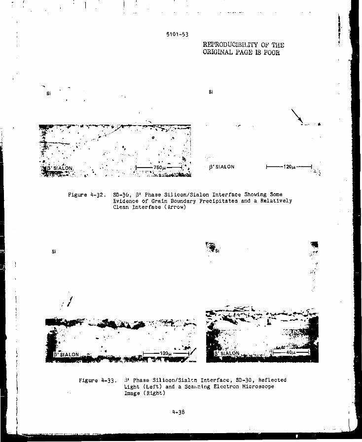
5101-53
REPRODUCIBILITY OF THEORIGINAL PAGE 18POOR
$i
• • " , ,¢' ' -- o . t .,
• • _ , 750_
$i
,_' SIALON
\
I'_ 120_"------_.
Figure 4-32• SD-30, _' Phase Silicon/Sialon Interface Showing Some
Evidence of Grain Boundary Precipitates and a Relatively
Clean Interface (Arrow)
Si
I
_i ¸
Figure 4-33. F_' Phase Silicon/Sialcn Interface, SD-30, Reflected
Light (Left) and a Scahn_ng Electron Microscope
Image (Right)
4-38
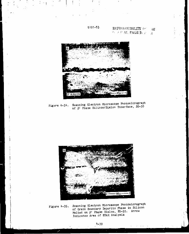
!
i
5101-53R EPT_O1)U(Y1]ILI_ ( ,. .t_:., i"A[, PAGE IS j ._
Figure 4-34. Scanning Electron Microscope Photomicrograph
of _' Phase Silicon/Sialon Interface, SD-30
Figure 4-35. Scanning Electron Microscope Photomicrograph
of Grain Boundary Impurity Phase in Silicon
Melted on @' Phase Sialon, SD-30. Arrow
Indicates Area of EDAX Analysis
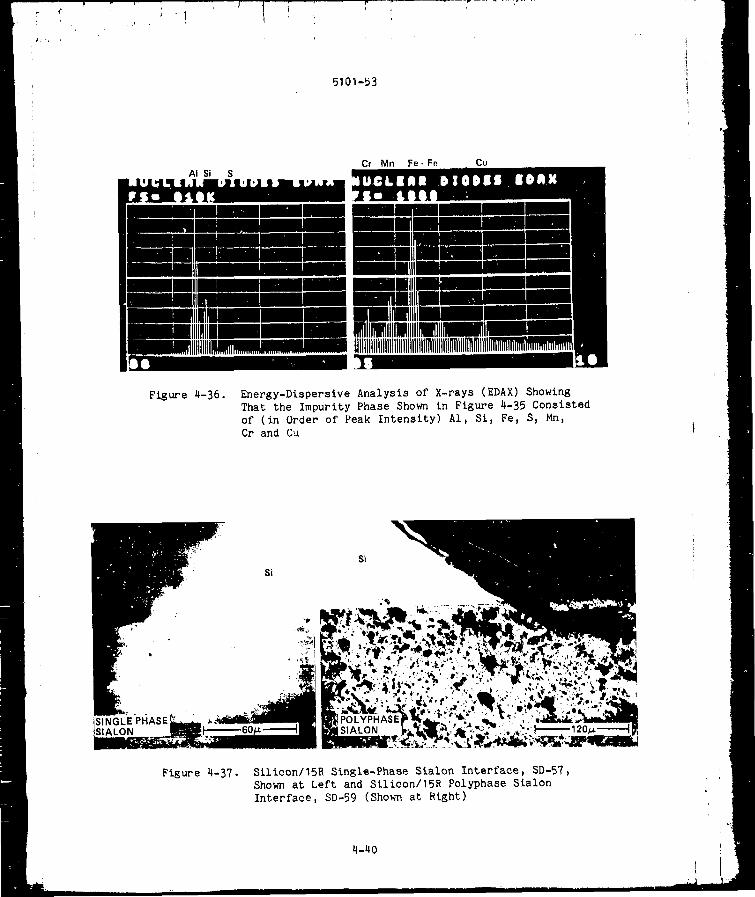
5101-53
AI Si SCr Mn Fe- Fe Cu
1111111
Figure 4-36. Energy-Disperslve Analysis of X-rays (EDAX) Showing
That the Impurity Phase Shown in Figure 4-35 Consisted
of (in Order of Peak Intensity) AI, Si, Fe, S, Mn,
Cr and Cu
si
Si
Figure 4-37. Sillcon/15R Single-Phase Sialon Interface, SD-57,
Shown at Left and Silicon/15R Polyphase Sialon
Interface, SD-59 (Shown at Right)
4-40

_I01-53
$i
J---_ 120p. -----_
Figure 4-38. I_:_urlty Phases in Silicon Melted on Sialon Material,
SD-_9, as-Polished
I -'_'-_._',t:'%.-.':2"',_ : ',"" _' .I _,.".-'o-;.g
r.;--._.._._'" "-:-,,.'_7-_,_",__ , _ ',.:_i_,_. _,4,,,.%,,.[__'.,..!.,,,,
Figure 4-39. Typical Polyphase Sialon Material, SD-60,as-Pol ished
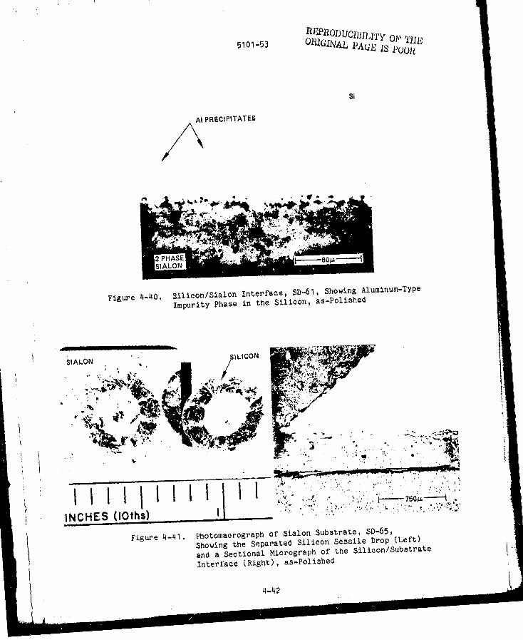
5101-53 R_RODUCIIJflJ'I,'Y. OP TIII_O,P.,ioL_,K/.,.PAGE 18 POOI_ '
si
i
Figure 4-40. Silicon/Sialon Interface, SD-61, Showing Aluminum-Type
Impurity Phase in the Silicon, as-Polished
$1ALON , • SILICON __
p,-• -_,,.11_" • _ -. _ ".,_._ _-,_.. _ i_l_l I
y-
tlllllllINCHES (lOths)
, , , l , • , , ,
I111..__ ; v_.__rh ..:T,:r_.
,.. , . , .
Figure 4-41. Photomaerograph of Sialon Substrate, SD-65,Showing the Separated Silicon Sessile Drop (Left)
and a Sectional Micrograph of the Silicon/Suhstrate
Interface (Right), as-Pollshed
4-42
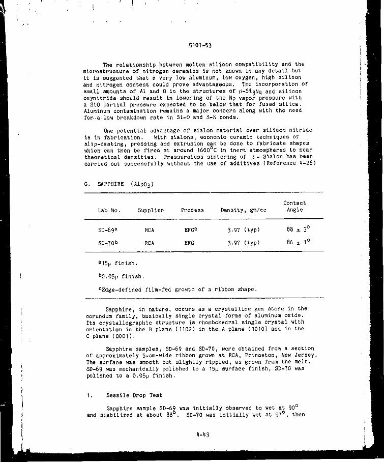
5_01-53
The relationship between molten silicon compatibility and the
microstructure of nitrogen ceramics is not known in any detail but
it is su___ested that a very low aluminum, low oxygen, high silicon
and nitrogen content could prove advantageous. The incorporation of
small amounts of A1 and 0 in the structures of i_-Si3N4 and silicon
oxynitride should result in lowering of the N2 vapor pressure with
a SiO partial pressure expected to be below that for fused silica.
Aluminum contamination remains a major concern along with the need
for-a-low breakdown rate in St-O and S-N bonds.
One potential advantage of sialon material over silicon nttrlde
is in fabrication. With sialons, economic eeramle techniques of
sllp-castlng, pressing and extrusion can be done to fabricate shapes
which can then be fired at around 1600°C in inert atmospheres to near
theoretical densities. Pressureless sinterlng of _- Sialon has been
carried Out successfully without the use of additives (Reference 4-26)
G. SAPPHIRE (A1203)
Contact
Lab No. Supplier Process Density, gm/ce Angle
SD-69 a RCA EFG e 3.97 (typ) 88 z 3°
SD-70 b RCA EFG 3.97 (typ) 86 ± I°
a15w finish.
bO.05_ finish.
eEdge-deflned film-fed growth of a ribbon shape.
Sapphire, in nature, occurs as a crystalline gem stone in the
corundum family, basically single crystal forms of aluminum oxide.
Its crystallographic structure is rhombohedral single crystal with
orientation in the R plane (1102) in the A plane (1010) and in the
C plane (0001).
Sapphire samples, SD-69 and SD-70, were obtained from a section
of approximately 5-cm-wtde ribbon grown at RCA, Princeton, New Jersey.
The surface was smooth but slightly rippled, as grown from the melt.
SD-69 was mechanically polished to a 15_ surface finish, SD-70 was
polished to a 0.05p finish.
I. Sessile Drop Test
Sapphire sample SD-6_ was initially observed to wet at 90 °and stabilized at about 88 . SD-70 was initially wet at 97 °, then
4-43
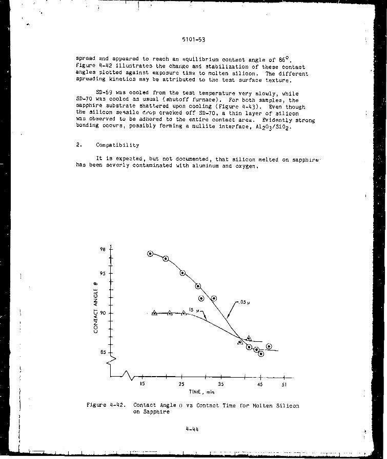
5101-53
spread and appeared to reach an equilibrium contact angle of 86 ° .
Figure 4-42 _llustrates the change and stabilization of these contact
angles plotted against exposure time to molten silicon. The different
spreading kinetics may be attributed to the test surface texture.
SD-69 was cooled from the test temperature very slowly, while
SD-70 was cooled as usual (shutoff furnace). For both samples, the
sapphire substrate shattered upon cooling (Figure 4-43). Even though
the silicon segsile deop cracked off SD-70, a thin layer of silicon
was observed to be adhered to the entire contact area. Evidently strong
bonding occurs, possibly forming a mullite interface, A1203/Si02.
2. Compatibility
It is expected, but not documented, that silicon melted on sapphire-
has been severly contaminated with aluminum and oxygen.
98
95
CD
Z<
90
85
Figure 4-42.
05
I I I I I I I _, -15 25 35 45 5 |
TIME, mln
Contact Angle 0 vs Contact Time for Molten Silicon
on Sapphire
4-44
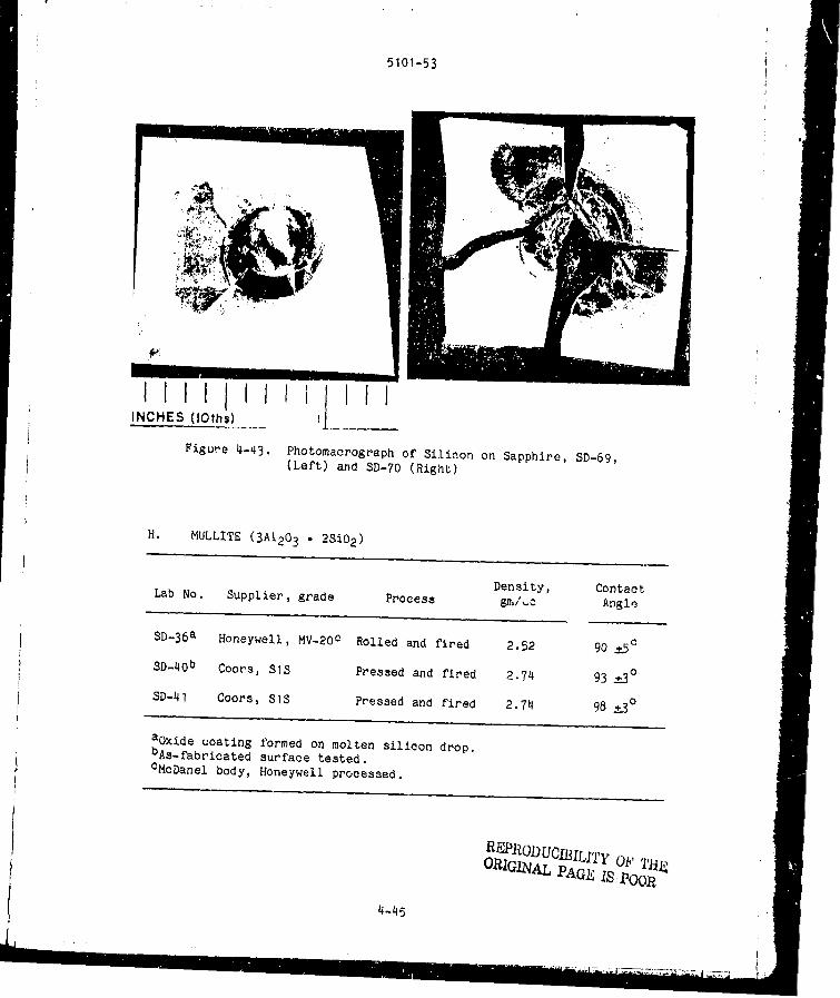
5101-53
Figuee 4-43. Photomacrograph of Silicon on Sapphire, SD-69,(Left) and SD-70 (Righb)
H. MULLITE (3A1203 • 2SiO 2)
Lab No.
Density, Contact
Supplier, grade Process _,_/_c Angle
SD-36 a
SD-40 b
SD-41
Honeywell, MV-20 e Rolled and fired
Coors, SIS Pressed and fired
Coors, SIS Pressed and fired
2.52 90 +_..5°
2.7_ 93 ...._o
2.74 98 +_3°
aoxide coating formed on molten silicon drop.bAs-fabricated surface tested.
CMcDanel body, Honeywell processed.
4-45
REPRODUCIBILITY OY 'I'.H_ORIGINAL PAGE IS POOR

Table 4-6.
5101-53
Emission Spectroscopy Chemical Analyses of Various
Mullites (Performed at Honeywell), wt %
McDanel (MV-20) McDanel (MV-30) American Lava
Fe 0.89 0.55 0.75
Ti 0.78 0.54 0.021
Mg 0.20 0.13 0.48
Ma 0.28 <0. I <0. I
Ca 0.11 <0.03 <0.03
Mn 0.041 0.01 <0.01
V 0.031 0.03 <0.01
Cu <0.01 _0.01 <0.01
Table 4-7. Typical Chemical Analysis of McDanel MV-20 andMV-30 Mullite, wt %
Compound MV-20 MV-30
AI203 55 4 60.0
Si02 42.0 38.0
K20 0.7 0.5
Na20 0.5 0.08
CaO 0.5 0.01
Fe203 0.8 0.5
TiO 2 0.5 0.5
MgO 0.04 0.2
4-46

I
• _ • _ , ,I,
5101-53
M,Jllite (3A120_ • 28i02) , manufactured by MeDanel, was rolled and fired
at approximately 1630°C by Honeywell and Mullite was also fabricated by Coors
in a somewh-t similar procedure. Coors samples were round discs approximately
2.54 cm (I i_.) in diameter by .48 cm (3/16 in) thick, while Honeywell's samples
were unevenly flat, approximately .16 cm (I/16 in) thick, rectangular shapes.
Honeywell Corporate Material Sciences Center (Reference 4-29) has
been involved with the technical and economic feasibility of producing
solar-cell-quality sheet silicon by applying a thin coating of silicon
on an inexpensive ceramic substrate. Mullltc, protectively coated
or not, has been and is still being considered the main candidate sub-
strate material. Optimization of the AI203/SiO 2 composition, however,
has not yet been accomplished.
The Honeywell Chemistry Laboratory used emission spectroscopy to
identify impurities in three candidate ceramic bodies (Tables 4-5 and 4-6):
(I) McDanel MV-20 rolled, dried and fired mullite.
(2) MeDanel MV-30 slip-cast mullite.
(3) American Lava hot-pressed mullite.
McDanel MV-20 was the only material tested in the JPL study.
Honeywell has concluded that the di_ coating process will probably
require a mullite substrate with a composition containing an excess
of Si02 in order to better match the thermal coefficient of silicon.
Even though the contact time between the mullite substrdte and
molten silicon is very short, dissolution of the mullite still occurs
rapidly in the first few minutes. It appears that the aluminum impurity
level of the melt increases rapidly during the first 2 or 3 minutes
of contact time with the substrate, and then increases exDenentially
at a lesser rate, becoming very nearly saturated after an hour of contact
time (Reference 4-30).
Indications that the dissolved aluminum and other impurities
transferred to the molten silicon are electrically active can be
observed in plots of electrical resistivity vs accumulated time of
exposure to mul) ite (Figure 4-44). A layer of carbon on the mullite
surface has been used to effectively reduce this contamination problem.
However, _-SiC has been observed to form (Figure 4-45).
I. Sessile Drop Tests
Observations from sessile drop tests were (I) mullite exhibited
what can be considered a borderline to nonwettlng property (equilibrium
contact angles0 _95°); (2) an oxide-type coating formed on the molten
silicon, SD-36, and may have influenced its wetting behavior; (3)
interface bubbling occurred, which is a possible indieaticn of Si0
evolution; and (4_ a rougher as-fabricated surface, SD-40, exhibited
a contact angle 6 less than a polished surface.
4--47

I iI
5101-53
>
;00
I.O
O.I
- ' I
_ MELT 28
' I ' I" ' I ' I = I '
Q-- LAYER R[SISTIVITIFS
r_- MELT RE_ISTIVITI[S
e4FLT 29 -_Ip-l!'_
m f D I _ I _ 1 L ( l I L .,I0 20 30 40 Sr_ _3 7n
;ttr (r:tn)
Figure 4-44. Layer and Melt Resistlvltles vs Accumulated
Time That the Respective Melts Were Exposedto Mulllte (Reference 4-29)
4-48

5101-53
CJ
<zl_
V_t_v_
E
Z0U
V_
20 #m
£
J
I
§
4-49

5101-53
2. Compatibility
Both bulk grain boundary and near interface impurity phases were
present in the silicon melted on mullite from Honeywell, SD-36 (Figure 4-46).The grain boundary impurity elements consisted of a two-phase precipitation
(Figure 4-47). Energy dispersive analyses of X-ray (EDAX) measurements
were made on these precipitates and results indicate the white phase(A) to be a high silicon/low aluminum alloy and the whlte/black pepper
phase (B) to be a high aluminum/low silicon alloy. Aluminum and siliconform a eutectic which contains 11.7 wt% Si and melts at 577°C. All
along the mullite/silicon interface, within approximately 10 microns
(0.004 in) of the mullite surface, silicon oxide precipitates were
observed (Figure 4-48). These precipitates were believed to be SiC2because EDAX count readings on these particles were nearly identical
to readings taken on the Si02 phase in the mullite substrate (Figure 4-49).Actual determination of chemical contents of these impurity phases
would require oxygen-detecting methods such as the ion microprobe.
Silicon melted on mullite from Coors, SD-40 and SD-_I, exhibited
(I) silicon penetration 635 microns (0.025 in.) into the mullite pores,
which occurred only in the center portion of the molten silicon contact
area (Figure 4-50), (2) no interfacial phase formations, (3) similarity
to SD-36, in that AI-Si eut_ctic phases were present in the silicon matrix,
and (4) high elemental impurity doping levels as revealed by semiquantitative
analysis (Table 4-I). These impurities included, but were not limitedto, aluminum, iron and titanium. T±tanium has a very drastic effect
on electrical efficiency (Figure I-5).
I. SILICA (Si02)
Density, Contact
Lab No. Supplier Process gm/cc Angle
SD-54 General Electric Fused 2.18 92_+_3°
SD-56 Thermo-Sil Slip-cast 2.18 91 ±2 °
All forms of silica, when heated to sufficiently high temperatures,fuse and form amorphous silica glass or fused silica. Fused silica,
SD-54, was obtained from General Electric in the form of a 30.5 cm (12-in.)diameter crucible dish 0.64 cm (1/4-in.) thick. Slip-cast silica, SD-56,
1.9 cm (3/4-in.) thick, was obtained from Thermo-Sil. Table 4-7 shows
data on typical impurity levels in GE-204 fused silica.
Fused silica has been the major material used in containing molten
silicon. There are, however, several problems encountered with its use.
Molten silicon reacts with SiO 2 in the following manner:
Si (i) ÷ Si02 (s)_2SiO(g)
4-50
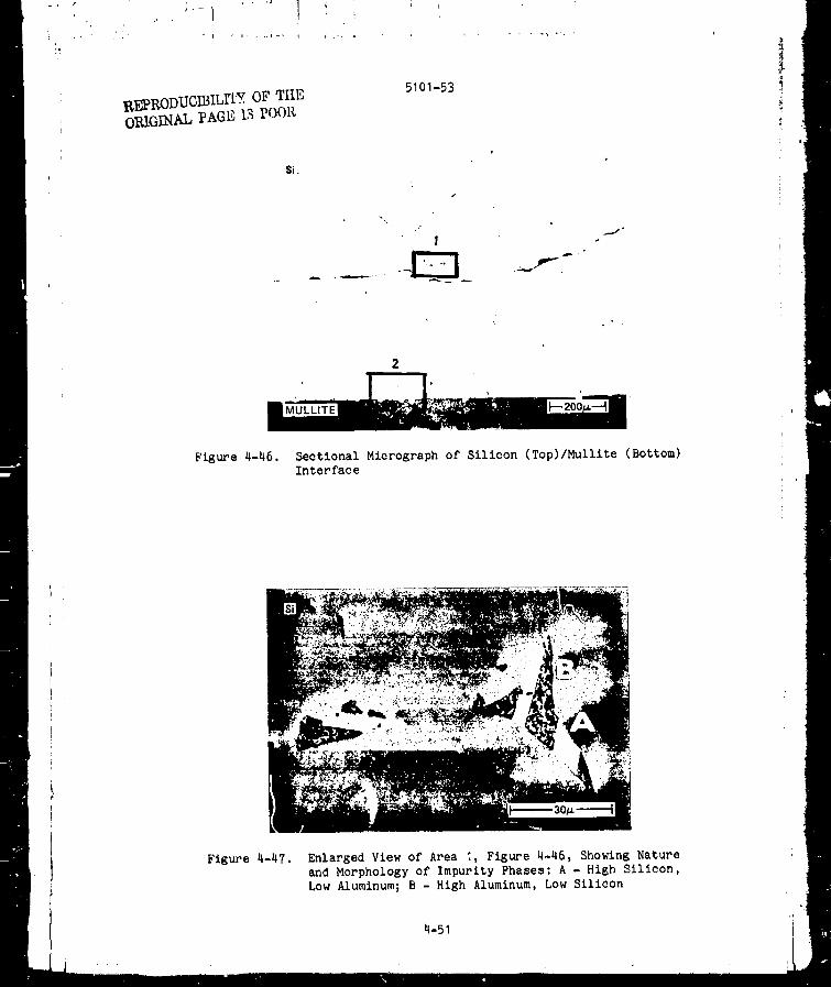
- _ _ _ - .i-, _ s -_ 4 i
R]_RODUCIBILFI'.v. OF THE
ORIGII_1AL PAGI_ 13 POOR
$i.
5101-53
/
/
!
Figure 4-46. Sectional Micrograph of Silicon (Top)/Mullite (Bottom)Interface
Figure 4-47. Enlarged View of Area :, Figure 4-46, Showing Nature
and Morphology of Impurity Phases: A - High Silicon,
Low Aluminum; B - High Aluminum, Low Silicon
4-51
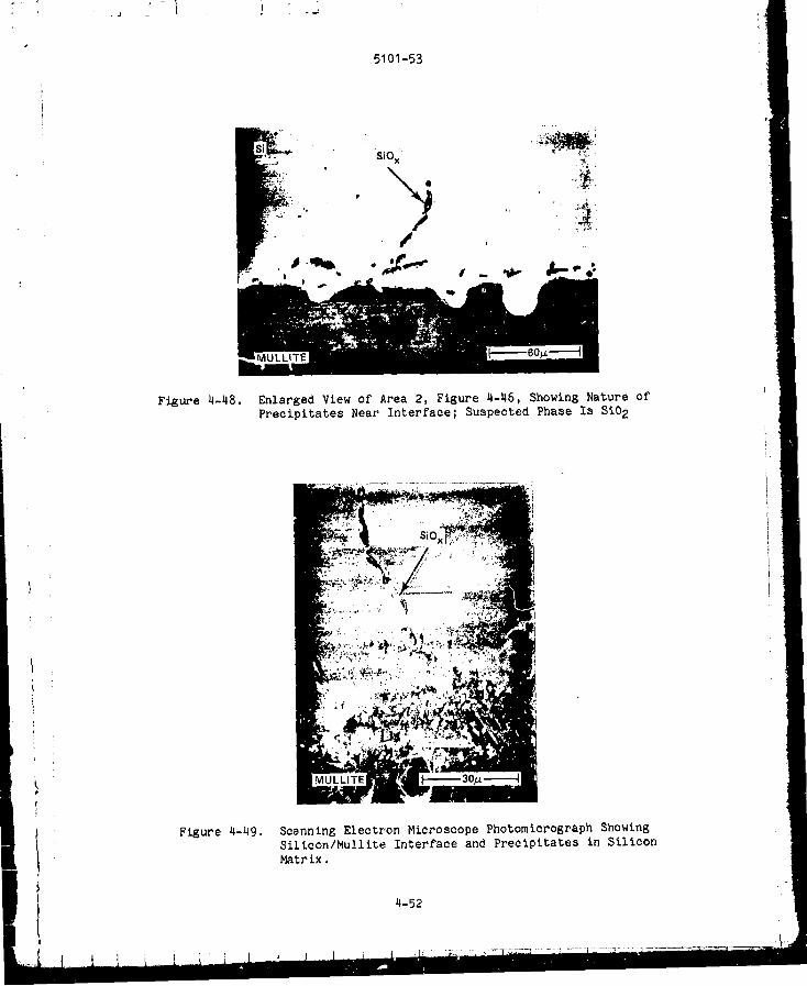
! ! .L
5101-53
$iOx'
l
Figure 4-48. Enlarged View of Area 2, Figure 4-46, Showing Nature ofPrecipitates Near Interface; Suspected Phase Is SiO 2
Figure 4-49. Scanning Electron Microscope Photomicrograph ShowingSillcon/Mulllte Interface and Precipitates in Silicon
Matrix.
4-52

L
5101-53
I+J.]PI{(-_DUC_II+[I,ITY OT_ q_TP,
(_i,i:l .\ l, ',.',_' ]_: [_),t[_,
$i
!
$i
Figure 4-50. Sectional Micrograph of Silicon/Mullite Interface,
SD-40, Showing Silicon Penetration Into Mullite
Porosity, as-Polished
After a period of time, SiO vapors build up on surfaces above
the pool of molten silicon. These layer deposits will flake off, drop
into the molten silicon and act as nucleation sites, causing single-crystal Czochlarski boules or ribbons to become polycrystalline in
structure. In addition, since the fused silica is being dissolved,
any impurities in it are also being added to the melt along with oxygen.
Silicon saturated in oxygen will typically contain 1018 atoms/cm3,which can influence the semiconductor properties of silicon considerably
(Reference 4-31). Though there is a contamination problem, generally
acceptable solar cells (_15% efficiency) have been and are being fabri-
cated from sliced Czochlarskz ingots drawn from fused silica crucibles.
Mobil-Tyco (Reference 4-32) encountered an aluminum contamina-
tion problem in EFG grown ribbon when a 15.24 em (6-in.)-long fused
silica crucible was used. The crucible length has since been
decreased to 10.16 cm (4-in.) to bring the ratio of the crucible
surface-to-melt volume closer to that existing in induction furnace
growth systems in which the aluminum adsorption was rarely observed.
Fused silica crucibles used in ribbon and ingot fabrication continue
to be a major cost item. Molten silicon left in the bottom of the crucible
bonds to the fused silica, and because of differing thermal expansion co-efficients, both silicon and container usually fracture during cooling. Thisoccurs below 650°C (Reference 4-33). Also, softening and devitrification
4-53
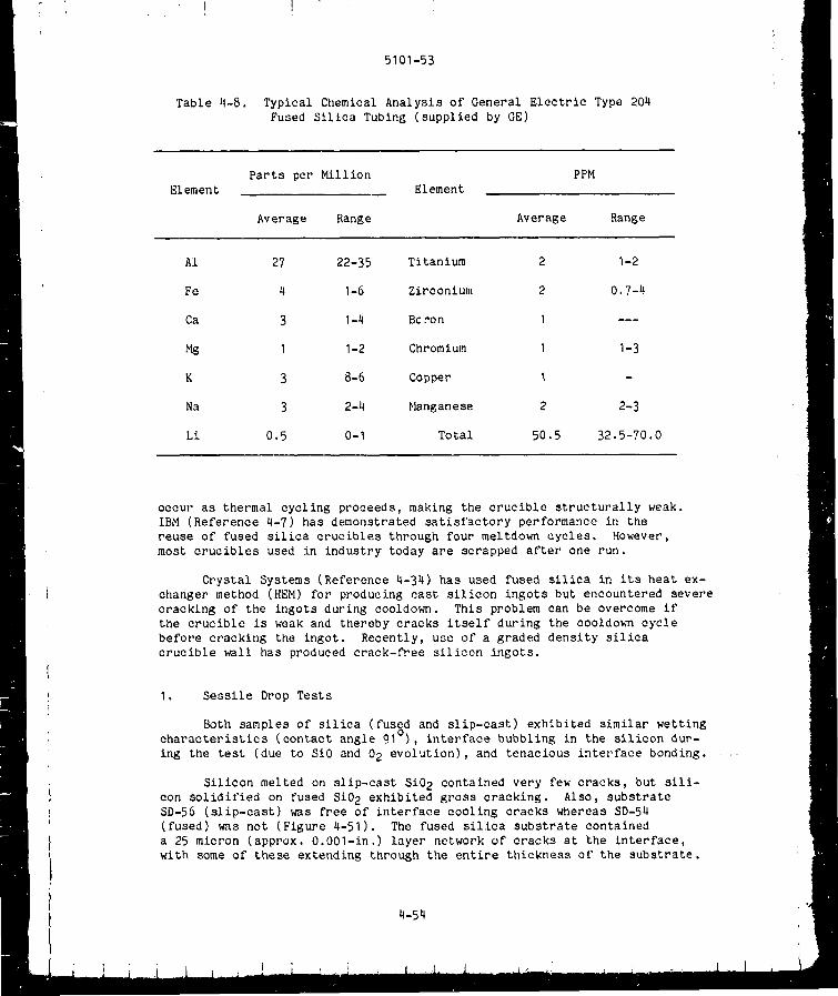
I J
Table 4-8.
5101-53
Typical Chemical Analysis of General Electric Type 204
Fused Silica Tubing (supplied by GE)
Parts per Million PPM
Element Element
Average Range Average Range
AI 27 22-35 Titanium 2 I-2
Fe 4 I-6 Zirconium 2 0.7-4
Ca 3 1-4 Be ._on I ---
Mg I 1-2 Chromium I 1-3
K 3 8-6 Copper I -
Na 3 2-4 Manganese 2 2-3
Li 0.5 0-I Total 50.5 32.5-70.0
occur as thermal cycling proceeds, making the crucible structurally weak.
IBM (Reference 4-7) has demonstrated satisfactory performance in the
reuse of fused silica crucibles through four meltdown cycles. However,
most crucibles used in industry today are scrapped after one run.
Crystal Systems (Reference 4-34) has used fused silica in its heat ex-
changer method (HEM) for producing cast silicon ingots but encountered severe
cracking of the ingots during cooldo_. This problem can be overcome if
the crucible is weak and thereby cracks itself during the cooldown cycle
before cracking the ingot. Recently, use of a graded density silica
crucible wall has produced crack-free silicon ingots.
I, Sessile Drop Tests
Both samples of silica (fused and slip-cast) exhibited similar wetting
characteristics (contact angle 91°), interface bubbling in the silicon dur-
ing the test (due to SiO and 02 evolution), and tenacious interface bonding.
Silicon melted on slip-cast SiO 2 contained very few cracks, but sili-
con solidified on fused Si02 exhibited gross cracking. Also, substrate
SD-56 (slip-cast) was free of interface cooling cracks whereas SD-54
(fused) was not (Figure 4-51). The fused silica substrate contained
a 25 micron (approx. O.O01-in.) layer network of cracks at the interface,
with some of these extending through the entire thickness of the substrate,
4-54
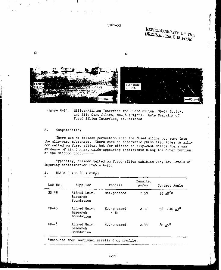
5101-53
$i
';::: ,.. _,:,_j/._." :'L',_ _' " '
Figure 4-51. Silicon/Silica Interface for Fused Silica, SD-54 (Left),
and Slip-Cast Silica, SD-56 (Right). Note Cracking ofFused Silica Interface, as-Polished
2. Compatibility
There was no silicon permeation into the fused silica but some into
the slip-cast substrate. There were no observable phase impurities in sili-
con melted on fused silica, but for silicon on slip-cast silica there was
evidence of light gray, oxlde-appearlng precipitate along the outer portionof the silicon drop .........
Typically, silicon melted on fused silica exhibits very low levels ofimpurity contamination (Table 4-3).
J. BLACK GLASS (C • Si02)
Density,Lab No. Supplier Process gm/cc Contact Angle
SD-45 Alfred Univ. Hot-pressed 1.58 95 _%5°aResearchFoundation
SD-46 Alfred Univ. Hot-pressed 2.17 56--46 +_3°Research _ BNFoundation
SD-48 Alfred Univ. Hot-pressed 2.33 82 +_5°ResearchFoundation
aMeasured from sectioned sessile drop profile.
5101-53
All black glass samples were prepared at the Alfred UniversityResearch Foundation in New York. SD-45 was an air-cooled sample fabricated
by hot-presslng Cabosil and Carbowax in a graphite die to 68% of theoretical
density. SD-46 was a hot-pressed mixture of silicle acid, carbowaxand a small amount of boron nitride. SD-48 was furnace-cooled after
hot-pressing silicic acid and carbowax to its theoretical density.All samples were I/4-in. thick and 2 in. in diameter.
"Black glass" is a general term used to describe an amorphous
silica glass having carbon distributed through its structure. The
exact way in which this carbon is placed in the silica glass has been
described by C. F. Smith in his Ph.D. thesis at Alfred University entitled"The Vibrational Spectra of High Purity and Chemically Substituted
Vitreous Silicas", dated May 1973. Patent No. 3378431, "Method of
Making C-Containing Glass and Products Thereof", was granted in 1968to C. F. Smith and W. 0. Crandall.
The difference between ordinary or clear amorphous (fused) silica and
black glass is not just in the color, but also in its properties. Black
glass has been found to have superior resistance to devltrification aboveI000°C, where ordinary fused silica has an increasing tendency to crystallize
and destroy itself. All other features of black glass, like high thermal
shock resistance, etc., are quite similar to ordinary fused silica.
!
I. Sessile Drop Test
Photographic records of contact angles on SD-45 were not
possible because the outer circumferential portion of the substratebegan and continued to uniformly warp upward when the temperatureexceeded about 1300°C. The contact angle was measured on the post-test
mount section. When the sample was removed from the furnace it was
observed that the properties of the black glass had significantly
changed. Density was much lower, physical dimensions had enlargedand the material was friable. Wetting angle measurements on SD-48
were also difficult to obtain due to high temperature (>13OO°C) glazing
of the test surface and.some warpage of the outer circumference.
No substrata warpage occurred with SD-46, which made in situ contact
angle documentation possible. The contact angle on SD-46 appeared tostabilize at 46° after approximately 20 min of contact time. However,
as noted with both other tests, SD-45 and SD-48, an oxide-type film
appeared on the silicon during the test.
The silicon sessile drop "popped off" on samples SD-46 and SD-48
(Figure _-52) but remained intact on SD-45.
2. Compatibility
All samples showed evidence of carbide-type precipitates havingformed in the molten silicon. These silicon carbide-appearlng particles
were generally found near the free surface of the silicon drop. The
carbide quantity was considerably lower than for silicon melted on
_-56

_101-53
-_mmmmm,_,=--
O
Figuee 4-52, Photomacrograph of Black Glass SD-48, Showing
Substrate Surface Glazing and Separated Silicon
Sessile Drop (at RiKht)
carbon and SiC products. This fact tends to indicate a greater chemical
stability for molten silicon/black glass material systems. Silicon
did permeate SD-45 (Figure 4-53) but not SD-46 or SD-_8, These last two
substrates showed a general lack of interfaclal reactions, Semi-
quantitatlve chemical analysis of silicon melted on SD-46 revealed a
contamination level of boron greater than 500 ppm (Table 4-I).
This level was much lower than for silicon melted on boron nltride;
however, it is still detrimental. No other elements were found in any
excess, but carbon and oxygen levels were not determined.
3. Discussion
Reasons for the wide variation in observed contact angles are not
known. Preliminary analysis indicated that both chemical and mechanical
stability of the black glass in the temperature range of interest are
dependent on the fabrleatlon technique, Therefore, material developed
and tested in this program may not truly characterize its inherent
properties, Black glass wetting and potential nonoontamlnation properties
indicate a material that should not be eliminated from further testing
and evaluation as improvements are made.
4-57

5101-53
BLACKGLASS
Figure 4-53. Silicon on Black Glass, SD-45; Photomacrograph (Left) is
Approximately 5X. Photograph (40X) on Right is a Close-
up View of the Silicon/C • SiO 2 Interface Showing .....
Silicon Penetration
K. BORON NITRIDE (BN)
Lab No. Supplier (grade) Process
Density,
gm/ee
Contact
Angle
SD-16 a Union Carbide
SD-17 a Union Carbide (HER)
SD-19 a Union Carbide (HBR)
SD-20 b Duramic Products c
Pyrolytic
Hot-pressed
Hot-pressed
Hot-pressed
2.19
P.03
2.03
2.12
O112± 3
146_ 4 _
145± 3 °
136± 4 °
aAs received, surface-tested.
b61_ surface finish-tested.
CA subsidiary of Kawecki-Berylco Ind.
4-58

5'101-53
Pyrolytic boron nitrlde, Boralloy, SD-16, was fabricated by Union
Carbide. It is a pure, opaque-white, gas-deposited composite whichis a highly oriented anisotropic crystalline material. Some typical
property data (supplied by Union Carbide) is glven betow:
Total Thermal Expansion
12.7 microns/mlcron (0.0005 In./in.)"a" direction
at 260°C (500°F)
"a" direction
at I093°C (2000°F)
(LinEar) "e" direction
at I093°C (2000°F)
43.2 microns/micron
1016 microns/micron
(0.0017 in ./in. )
(0.040 in./in .)
Total Chemical Impurities <100 ppm
Solid boron nitride samples, SD-17 and SD-19, UCAR grade HBR, were
made by Union Carbide. Hot-pressed BN, SD-20, was supplied by Kawecki
Berylco Ind. This type of sample is typically prepared by hot-presslngpowdered BN at approximately 1982°C (3600°F) and 6.9 x 100 N/m 2 (1000
psi). As a result, the BN polymerizes to form a structure similar tothe anthracene ring. Subsequent fabrication is usually accomplished
by machining the hot-pressed cylinders to finished tolerances.
Typical chemistry data for hot-pressed BN (supplied by Duramic
Products) is as follows:
Composition Regular Low Oxygen
%BN 96.0 99.0
%N2 54.0 55.99
%B 42.70 43.40
%C 0.20 0.20
%02 3.09 0.40
% others 0.01 0.01
i
5101-b3
Some general property data for hot-pressed BN (supplied byDuramic Products) is given below:
Thermal AgainstConductivity Grain With Grain
302°C (575°F) 5.3 (10)
982°C (1800°F) 4.3 (8)
12.8 (24) W/m-k (Btu/hr-Ft-°F)
9.6 (18) W/m-k (Btu/hr-Ft-°F)
Coefficient of Against
Thermal Expansion Grain With Grain
75 - 700°F 142 (56) 7.6 mlm/k • 10-9
(3 in.lin./°F ' 10-7)
75 - 1650°F 114 (45) 12.7 m/m/k • 10-9
(5 in./in./°F • 10-7)
75 - 1850°F 102 (40) 10.2 m/m/k • 10-9
(4 in./in./°F • 10-7)
When BN is heated above 1200°C (2190°F), 80% of expansion remains
as permanent set.
Special handling of boron nitride samples was incorporated intothe lab, since experience had shown that contact with water and sub-
sequent heating caused interlamellar flaking. This material is also
attacked by carbon tetraehloride, alcohol and acetone.
I. Sessile Drop Tests
It appeared that the wetting characteristics of pyrolytic BN
were inherently different from hot-pressed BN. On pyrolytic BN,SD-16, a contact angle 20% lower than for silicon on hot-pressed BN
was observed. The presence of a highly oriented surface crystallo-graphic plane is thought to be the reason for this difference.
Hot-pressed BN from Kawecki Berylco exhibited a slightly differentcontact angle (about 5% lower) than the Union Carbide product. This
effect may be the result of different sample histories (note densityvariation) and/or the surface texture tested, i.e., 6_ finish for SD-20
vs as-fabricated surface for SD-17 and SD-19. Further sessile drop
tests were n_,eded to fully clarify the wetting properties of varioushot-pressed i_N products but were not conducted in view of the high Bcontent observed in the Si.
4-60
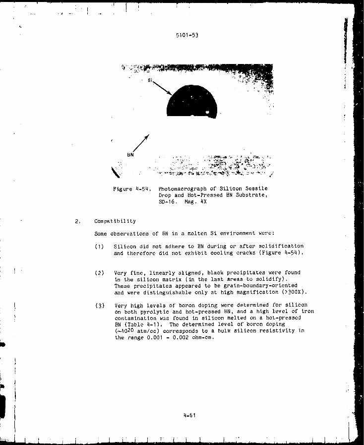
1
5101-53
fan
Figure 4-54. Photomacrograph of Silicon Sessile
Drop and Hot-Pressed BN Substrate,
SD-16. Mag. 4X
2, Compatibility
Some observations of BN in a molten Si environment were:
(I) S_lleon did not adhere to BN during or after solidification
and therefore did not exhibit cooling cracks (Figure 4-54).
(2)
(3)
Very fine, linearly aligned, black precipitates were found
in the silicon matrix (in the last areas to solidify).
These precipitates appeared to be grain-boundary-oriented
and were d_stlnguishable only at high magnification (>300X).
Very high levels of boron doping were determined for silicon
on both pyrolytic and hot-pressed BN, and a high level of iron
contamination was found in silicon melted on a hot-pressed
BN (Table 4-I). The determined level of boron doping
(_I020 atm/cc) corresponds to a bulk silicon resistivity in
the range 0.001 - 0.002 ohm-cm.
4-61

L
5101-53
L. HAFNIA (HfC2) and HAFNIUM CARBIDE (HfC)
Density, Contact
Lab No. Supplier Process (material) gm/ce Angle
SD-32 a Ultramet Vapor-deposlted (Hf02) 9.68 b 78 ±3 °- O°e
SD-33 a Ultramet Vapor-deposlted (HfC) 12.20 b <5 °
aAs-deposited, surface-tested.
bTheoretical density.
cSilicon absorbed into graphite substrate.
Hafnla, SD-32, and hafnium carbide, SD-33, were both chemical-
vapor-deposlted on 5.08 cm (2-in.)-diameter graphite substrates by
Ultramet in Pacoima, Calif. Hf02, SD-32, which has a melting point
of 2610°C, was deposited by reacting hafnium chloride (HFCI4_ , oxygen(02), hydrogen (H2), and saturated water vapor (H20) at 1400 C in the
presence of a graphite substrate. HfC, SD-33, which has a calculated
melting point of 3890°C (Reference 4-35), was deposited by reaetin_
hafnium chloride (HfC14) , methane (CH4), and hydrogen (H 2) at 1400_C
in the presence of a graphite substrate.
I. Sessile Drop Test
Silicon melted on HfO2, SD-32: (I) exhibited an initial contact angle
of approximately 78 ° and (2) was absorbed into the graphite substrate through
cracks in the CVD layer (Figure 4-55). Mudcracklng patteens were evidence in
the HfO 2 layer in and around the molten Si contact area. Four major cracks
extended into the graphite substrate such that graphite acted as a wick and
completely absorbed the molten Si drop in 25 minutes total contact time.
HfC, SD-33, was wet immediately and completely by molten Si (Figure 4-56).
No contact angle was measured, but it _s _viously below 5° .
2. Compatibility
CVD HfO 2 on graphite, SD-32, appeared to be mechanically unstable,
due to cracking, in the presence of molten Si. Chemical reactions
in the HfO2/molten Si material system were not observed because the
silicon was absorbed into the graphite substrate. Molten St on HfO 2
would be expected to react with the Hf in the CVD layer, forming hafnium
silicides (Reference 4-36).
Molten Si in contact with CVD HfC, SD-33, reacted extensively
and formed several new hafnium silicide phases (Figure 4-57). Complete
idertiflcatlon of these phases was not determined.
4-62

JL
5101-53
,_ , + ,.,+..........
Figure 4-55. Hf02, SD-32 Post-Test SurfaceCondition Showing Absence of
Silicon, Mudcraektng Pattern
in CVD Layer and SubstrateCracks (Arrows)
M. YTTRIA (Y203)
Density,
Lab No. Supplier Process gm/ec Contact Angle
SD-31 Coors Hot-pressed 4.84 63 ±2 °
Yttria (Y203) , which melts at 2410°C, was supplied by the CeramicD_vlston of Coors, in Golden, Colorado. It was fabricated by hot-presslnga mixture to 97% of theoretical density. Polished sections of the
as-received sample revealed the presence of about 98% Y203 and 2% unknown
phase.
4-63
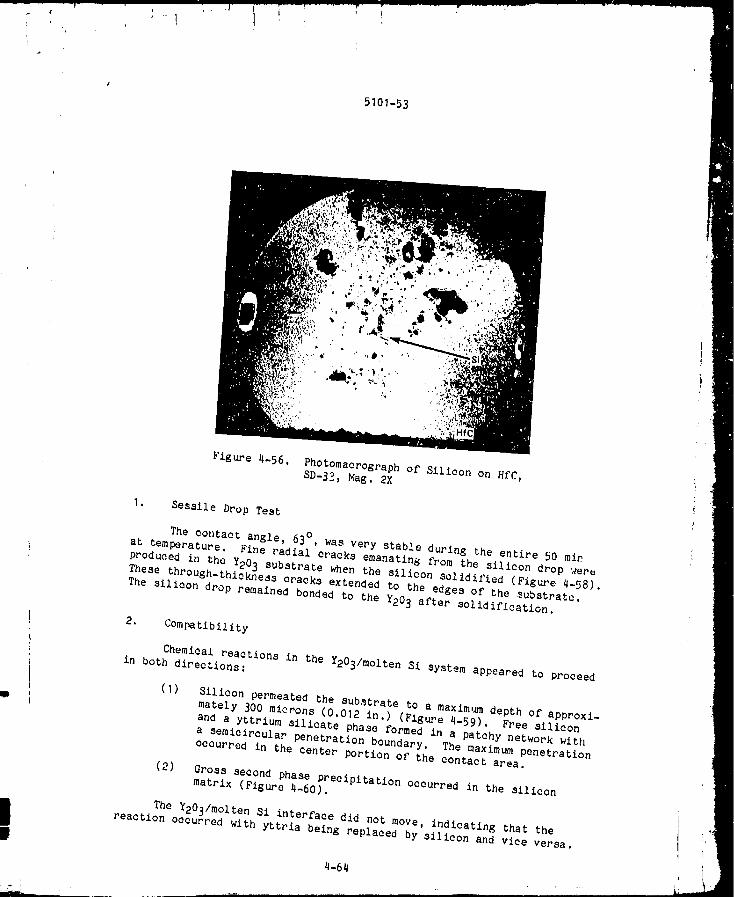
! l
5101-53
Figure 4-56. Photomacrograph of' Silicon on HfC,
SD-33, Mag. 2X
I. Sessile Drop Test
The contact angle, 63 °, was very stable during the entire 50 min
at temperature. Fine radial cracks emanating from the silicon drop wer_
produced in the Y203 substrate when the silicon solidified (Figure 4-58).
These through-thlckness cracks extended to the edges of the substratc.
The silicon drop remained bonded to the Y203 after solidification.
D
"_/n ml
2. Compatibility
Chemical reactions in the Y203/molten Si system appeared to proceed
in both directions:
Silicon permeated the substrate to a maximum depth of approxi-
mately 300 microns (0.012 in.) (Figure 4-59). Free silicon
and a yttrium silicate phase formed in a patchy network with
a semicircular penetration boundary. The maximum penetration
occurred in the center portion of the contact area.
(2) Gross second phase precipitation occurred in the silicon
matrix (Figure 4-60).
The Y203/molten Si interface did not move, indicating that the
reaction occurred with yttria being replaced by silicon and vice versa.
4-64
.=---q,m,J_

• [
RI:PI{(H_I '('l I",II .ITY rH; '1'1ll_
-, V .'_F j ii -_-/
_, p , "_ .HfC,
Figure 4-57. HfC/SilieoI_ Interface Region Showing the
Formation of Various Hafnium Silietdes,
as-Polished Condition. Arrow Indieates
OrigLnal CVD HfC Stlt'face
N. CERIUI, I SULPHIDE (CeS)
Density,
Lab No. Supplter Proce,,¢s gm/ee
SD-73 Electronic Hot-pressed 3.99
Space Pro-due t s
Contact Angle
_,.,0°--- 0
in q minutes
A fret-pressed disc 2.5 em (I in.) diameter, 0.64 em (I14 "in.)
thick, of cerium sulphide was supplied by Eleetroi_[c Space Products,
Ine., Los Angeles, Calif. CeS degrades at temperatures greater than
2100°C (Ref. 4-34).
4-(_%

5101-53
/
\Y203
ilZlllliJallalll| JL|r*_ u C" r I ,/_Ak.I
Figure 4-58. Top View of Sillcon on Y203SD-31, Showing Fin_ Craeks'(Arrows)
Emanating from Silicon Sessile Drop
$i
Figure 4-59. Sectional Maerograph of Sillcon/Y203 Interface,
SD-31, Showing Penetration of Silicon Into Y203Substrate
4-66

-. f
5_01-53
YITTRlUM, SILICIDE
.'x
Figure 4-60. Silicon Matrix, SD-31,
as-Polished. Mag 150X
1. Sessile Drop Test
(i) Silicon initially wet the CeS substrate at 50 ° . The molten
silicon was then absorbed into the substrate in approximately
5 minutes.
(2) CoS chemically and physically degraded in the presence
of molten Si at 1430°C. The post-sessile drop CoS
sample had expanded dimensions and was cracked and
friable (Figure 4-61).
2. Compatibility
(I) Silicon absorbed into the CeS structure formed a multitude
of new and complex phases (Figure 4-62).
(2) The reaction proceeded only one way, silicon into CoS,
so no data could be obtained on contamination levels in
the silicon.
(3) The material appears to have no potential for use in con-
tact with molten Si.
4-67
r
i
l 1iL I
i

J
! 1 :
5101-53
Figure 4-61.CeS, SD-?3, Showing the Post Sessile DropTest Surface (Left) and a Cross-Sectlonal
View Showing the Extent of Silicon Absorbtanoe
and the Dimensional Change in the CeS.
Figure 4-62.Sectional Micrograph of the Reacted Si + Ce + S
(Top _rea) and Unreacted Ce ÷ S (Lower Area). Mag 40X
4-68
REPRODUCIBILITY OF _[}IE
ORIGINAL PAGE IS P()_I}_

5_01-53
OoLANTHANUM HEXABORIDE (LAB6)
Density,Lab No. Supplier Process am/co Contact-Angle
SD-74 Electronic Hot-pressed 4.56 52 +_3°
Space Pro-ducts
A hot-pressed disc 2.5 em (I inch) diameter, 0.64 em (I/4 in.)
thick of lanthanum hexaborlde was supplied by the Electronic Space
Products, Inc. LaB6 has a melting point of 2210°C.
I. Sessile Drop Test
(i) Silicon wet LaB 6 and exhibited a mechanically stable contactangle of approximately 52 ° .
(2) The silicon cracked off the LaB 6 substrate during solidifi-cation, leaving a thin layer of silicon bonded to the sub-
strate (Figure 4-63).
2. Compatibility
(i) Several fine cracks 2-5 mm long originating from the SI/LaB 6
interface were observed in the LaB 6 substrate. The cracks,which were at right angles to the surface, were not filled
with silicon and are believed to have been caused by thermalstresses.
(2) Interestingly, for a material wet by silicon to 52 ° , there
was little or no silioon penetration or degradation of
the LaB 6 interface. The silicon material at the interface,however, appears to have undergone some reaction.
(Figure 4-63).
(3) Detrimental doping of the silicon melted on LaB 6 is highlyltkely but undocumented to date.
4-69

5101-53
-_ t:_S .._.,_
. ;" _'Z,_le, . _ _.: ,,j_, '..%,'_
.:.- .... ...,;:..
Figure 4-63. LAB6, SD-74, Showing Silicon Material Adheringto the Substrate (Left) and the Remaining
Si/LaB 6 Interface (right, magnification 200X)The Light Layer is the Silicon, Which ShowsEvidence of Reaction Products
REPRODUCIBIL1TY OF TttE
ORIGINAL PAGE IS POOR
4-70
¢
L
• j ,.
5101-53
SECTION V
SUMMARY
Molten Si acted as a solvent in various degrees on al] refractory
materials used as a sessile drop substrate. Research and compatibi) ity
studies conducted reveal that, to date, no ideal material exists which
will remain inert to a molten Si environment. However, several potentially
useful materials have emerged. Sessile deep tests conducted cate§orized
refractory materlal_ as "wetting" ((i < 85°), "nonwetting" ( (t> 95 )
or "borderli.e" (85- _ ()g 95v). Refractory material used for silicon
ribbon producing capillary dies must be wetting and nonreactive to
molten Si. Refractory material used for crucibles or containers may
be in any wetting category, yet, most importantly, must be nonreactive
to the molten St bath.
In relative order of importance, the four most desirable properties
that a refractory material in contact with molten Si must possess are:
(i) Lack of detrimental chemical reactivity (both intrinsic
and extrinsic).
(2) Wetting characteristics (only for capillary dies).
(3) Thermal/mecI1anical stability.
(4) Ease and low cost of fabrication.
Detrimental impurity contaminatlon is arbitrarily defined as
that impurity level which will cause electrical degradation below approxi-
mately 85% of a baseline (uncontaminated) efficiency. The baseline
cell is a P-type silicon having an accepter concentration in the 2.5
x 1015 to 7.0 x 10¹⁵ atoms/or range (Reference 1-13). Intrinsic chemical
contamination is defined as the detrimental dissolution, erosion, saturation
or precipitation of any element or compound into the silicon which
was initially part of the refractory material basic element structure,
e.g., carbon from SiC and aluminum from the A1203, structure. Extrinsic
chemical contamination is defined as the detrimental dissolution, erosion,
saturation or precipitation of any element or compound into the silicon
which initially was not a part of the refractory material basic structure.
Examples of this include magnesium from hot-pressed Si3N4, iron from
hot-pressed BN and calcium from sialon material.
OD the basis of the four properties listed above, as analyzed
from sessile drop tests, materiallographic studies, and/or chemical
analyses, the tested refractory materials were graded. (The following
list also reflects a refractory material potential for use in contact
with molten Si.)
5-I

5101-53
Refractory Mater_al/Multen Sf. Compatibility Rating
Chemical Wetting Test
Mater_al (Process) Compatibility Characteristic Rating Potential
Si3N4 (CVD) a Low I, low E W 5 4
Si3N 4 (HP) Low I, med. E W _ 4
_' slalon (HP) Med. I, med. E W 4 3
SiOXYN (RS) Unk. I, interface NW 2 4
phase reaction
15R, 8H polyphase Med. I, high E W 3 3sialon
SiC (HP) Med. I, med. E W 3 3
SiC (CVD) Med. _ (structure W 2 4
breakdown)
Low I, low E B 3 3
LOW I, med. E B 2 4
Med. I, low E W 3 2
Med. I, high E 5 2 3
Ned. I (structure W 2 3Unk E breakdom_)
Unk I, low E B 2 I
Med. I, low E W 2 I
Unk I, low _ W 2 I
High I, low E NW 2 0
High I, low E NW 2 0
Unk I, unk E W I 0
High I, unk E t_/, I Unk
SiC2 (fused)
Si02 (slip-cast)
Glassy carbon
3AI203.2SiO2 (P+F)
C'Si02 (HP)
AI203 (EFG)
C'SIO2 + BN (HP)
LaB 6 (HP)
BN (HP)
BN (CVD)
HfO2 (CVD)
Intermetallic
compound
5-2il
I i
5101-53
Refractory Material/Molten Si Compatibility Rating
Chemical Wetting Test
Material (Process) Compatibility Characteristic Rating Potential
SiC (sillconlzed) Absorbs silicon None 0 I
HfC (CVD) High I, ]ow E W 0 O
Me (rolled sheet) High I, _ow E W 0 0
CeS (}]P) Absorbs silicon W 0 Unk
aTcsted by RCA, Reference 1-18.
_brevieAion_
C%9 -ehemieal vapor deposition
lIP - hot-pressed
RS - reaction-sintered
P+F - pressed and fired
EFG - edged-defined film-fed growth
1 - intrinsic contamination
E - extrinsic contamination
_?ttiny, Ch_raeterlSt_c .Symbols
W - wetting
NW - nonwctting
B - borderline
5 - higIle_'_t i.atLn_, and potential Fop u:w Ln eontaet with molten
._it leon
0 - Lowe_'_t l'dL.[ll_ alh| II0 potential For u-m in contact with tno_ten
sillooll
A matepiaI max have a hiKhm' potential pat,lng than test paring.
it" It was felt that the speeIt'ie i'et'raeto.y mate.ial te:_ted did tlot
repl'esent the be,st quality malel'ial obtainable, A stlllil|lai'y of sill.con
compatibility factors Fop die, ¢ol/t:li.l_el' aud etib<atl'ate I'el'l'aetol'y illat.el'lals
is giVL'll below:
8ulTleieutly wet by Si (_ilO °, see Ptgul'e 11-1), thus could
be used ;is capillary dies.
Me.[tell silicon illhel'ently eaUlSes a pi'eeipitatioll oi' dissolution
of t_-8it: pai'tioles which al'e impai,ted into tl_e Si matl'ix.
011 soJ. idtl'ieation tile.so particles OatlSe 8ti'uctt,re bi'eakdOwll
In silieoll, which is eleetrioally active.
SiC pat-tiele eotitlt, appears to be l.owei" for. Si on SiC than
8i on C (glassy of gl'aphitie).
Silieou melted on low-deusity SiC coutaiuiug appl'ceiable
ailtoultt.s of l'l'ee silicon is abc_oi'bed into the substi'at.e,
1. SijN 4 exhibits sul't'ioieilt, wetting (_r+l°, see PJgtn'e _-I)
to be used as a capill:u'y die.
2. Very little illtet't'aet:iI reaetfon of dissolution was obset'ved
on hot-p/'ossed SijNll products,
_. Pi'e._enliy, tmpul'ity elelnents typieall.y l'ouild in SilNi I startii_g
powdOl'8 dppeal' t.o be the inhel'ent ¢ot/Iaillillat.ioll pl'oblem
I'o1' illOltiell _ilieon, Silicon Oll RS Si3Ni I e×llibti.ed higher
ootlt.alllindtloÁl levels ttldil silieoil on lip SiJN4.
II. PLII'e sitlgle-phase sill,!oil oxyuitrtde has yet to be tested
in contact wit:h molten silicon, Cotlliilel'clal-gi'ade polyphase
SiOXYN exhibilt, d llonwett.illg properties (0 k 115 ° ) aild thel'eI'ol'e
etlil be eonsidei'ed fop eOllt.ainel's of illvePt.ed l'ibboll gl'owth
dies.
4-11

5101-53
.
4.
5.
6Q
Various contact angle spreading rates were found for silicon
on 15R polyphase, 8H polyphase, X2 composition (two phase)and B' phase (single and poly) sialon material as evidenced
by the complex spreading klnettcs (Figures 4-30 and 4-31).
Single-phase material exhibited a lower kinetic spreading
rate than polyphase material.
High Initial wetting angles are attributed to a silicon
oxide layer usually present on starting powder surfacesor in polyphase material.
Materials tested in this program can be considered wettingwhen used in contact with molten St and are therefore candidates
for use as capillary dies.
Analyses tend to indicate that silicon is intrinsically
doped with A1 from the St-AI-O-N structure.
Extrinsic detrimental doping levels of iron, calcium andtungsten have been observed. These are impurities found
in starting powders.
I.
2.
3.
"Borderline" wetting properties (t__ 94 ° ) (see Figure 4-I).
Apparent intrinsic doping of silicon with aluminum.
Best match to the thermal coefficient of silicon.
I.
2.
3.
Borderline wetting properties (0 _ 86°).
Solidification of bulk Si on sapphire causes it to shatter.
Doping of Si with A1 is expected.
Black Glass (C.Si021
I. Valid wetting properties for a C.Si02,phase material werenot obtained. Tested material was not chemically or mechanically
stable at the test temperature.
2, Some substrates were observed to warp and glaze above 1300°C.
5-5
i i ......

5101-53
3,
4,
SiC precipitation was observed in the Si matrix, The rateand quantity of the SiC precipitation appeared to be lessthan for Si on C or SiC. .....
Small amounts of BN (_5%) caused detrimental doping ofSi with B.
Fused and SliD-Cast Silica
I, Both forms of silica exhibited similar borderline wetting
properties (O _ 91° ) (see Figure 4-I).
On solidification of Si sessile drops, more cracking was
observed in fused SiO 2 compared to sllp-east Si02.
. Silicon on fused SiO 2 contained the least impurities ofall materials tested.
4. Silicon on sllp-cast material contained visible impurity
phases (optically); none were observed for Si on fused SiO 2.
Boron Nitrlde
I. Nonwetting properties 0 _ 112 and 140° for CVD BN and
HP BN, respectively (see Figure 4-I).
2. Intrinsic detrimental doping of St with boron,
HfC, Hf09. Pvrolvtlc Grsphlte. Molybdenum, Cerium Sulphide, and
Sillconlzed.$11icon Carbide
These materials react extensively with molten Si and have no
potential for use in contact with molten Si.
Observations
1. Essentially no relationship existed between degrees of
wetting and the amount of bulk or interfacial chemicalreactions recorded.
2. Impurity elements present in single or polyphase refractory
material are potentially a source for silicon contamination.
3. Single-phase material appears more desirable than polyphase.
5-6
5101-53
REFERENCES
I-I . "Review, Silicon Solar Cells for Terrestrial Applications,"
j/_ Mater. Sci., Vol. 12, pp. 602-615, 1977.
I-2 . Vogel, L., Gardner, G., and Cave, E. F., U.S. Patent 3, Vol. 124,p. 489, 1964.
I-3. Work presently being conducted by University of South Carolinaand Westinghouse Electric Corporation.
I-4. "Large Area Silicon Sheet by EFG," First Quarterly Report 1977,
Mobil Tyeo Solar Energy Corporation, ERDA/JPL Subcontract No. 954355.
I--5 . Marumo, C., and Pask, J. A., "Reactions and Wetting Behaviour
in the Aluminum-fused Silica System," _. Mater. Sol., Vol. 12,
PP. 223-233, 1977.
I-6, Ahmad, U. M., and Murr, L. E., "Surface Free Energy of Nickel
and Stainless Steel at Temperatures Above the Melting Point,"J. Mater. S_,, Vol. 11, pp. 224-230, 1976.
I-7 . Swartz, J. C., "Atmosphere Effects on Wetting of Si3N 4 by LiquidSi," J. Am. Ceram. Soc., Discussion and Notes, Vol. 59 No. 5-6,
May-June 1976.
1-8 • Hoge, C. E., Brennan, J. J., and Pask, J. A., "Interracial Reactions
and Wetting Behavior of Glass-Iron Systems," J. Am. Ceram. Soe.,
Vol. 56, No. 2, Feb. 1973; also Battelle, Columbus Laboratories,Die and Container Material Develooment of the Large Area Silicon
Sheet Task 9_ the Low-cost Silicon Solar Array Project. Proposed
Research Program, Apr. I, 1977.
I-9. Champion, J. A., Keene, B. J., and Allen, S., "Wetting of Refractory Mate-
rials by Molten Metallides," J. Mater. Sci., Vol. 8, pp. 423-426, 1973.
1-10. Quincke, G., "Concerning the Capillary Constants of Molten ChemicalCompounds," Ann. Phys. Chemic, 138, 141, 1869.
1-11. Kingery, W. D., "The Role of Surface Energies and Wetting in
Metal-Ceramic Sealing," Ceram. Bull., Vol. 35, PP. 108-112.
1-12. Aksay, I. A., and Pask, J. A., "Phase Distribution in Solid-Liquid-
Vapor Systems," in "Surfaces and _nterfaces of Glass and Ceramics,"
Materials Science Research, Vol. 7, pp. 299-331.
1-13. Keck, P. H., and Van Horn, W., "The Surface Tension of Liquid
Silicon and Germanium Phys. Ray. Vol. 91, PP. 512-513, 1953.
1-14. Hopkins, R. H., et al., Silicon Materials Task of the Low Cost Solar
Array PrgJ_ct (Phase II), Westinghouse R&D Center, Quarterly Report
No. 6, ERDA/JPL 95_331-77/3, Jan. 1977-Mar. 1977; also McCormick,
J. R., Dow Corning Corp.
6-I
5101-53
1-15. Schmid, F. M., Analysis o_ Effects Of _mp_itle s Intcntlqqally
IncorDorate__into Silicon, Second Quarterly Report, 2 May 1977
- 29 July 15_7, ERDA/JPL Contract No. 954694.
1-16. Bates, h. E., and Leipold, M. H., personal communieBtion.
1-17. Cu]l_n, G., et al., Die and Container Material Development of
tile Large-Area Silicon Sheet Task of the Low-Cost Silicon Solar
Array Project, Pricing Proposed, PP 7?-032, Technical Proposal,
Part I, Radio Corporation of America, March 28, 1977.
1-18. Duffy, M. T., etal., Development and EYa!uation of Die Material
for Use in P_o.sL_eln_ Silicon RibbODS by the _ny@rte_ Ribbon Growth
_, First Quarterly Report Deeel_ber 1977, ERDA/JPL Contract
No. 954901, Radio Corporation of America.
1-19. Patel, J. R., and Batterman, B. W., J. ADpl. Phys. Vol. 34,
p. 2716, 1963; Disk Faraday See. Vol. 38, p. 201, 1964;
Soc. Ft. Flinera!r__Ci_$.t_g_l!_, Vol. 95, p. 700, 1972.
1-20. Kimerling, t. C., Leamy, B. J., and Patel, J. R., "The Electrical
Properties o_' Stacking Faults and Precipitates in Heat Treated
Dislocation Free Czoehralski Silicon," ADD1. Phys. Lett., Vol. 30,
No. 5, I Mar. 1977.
1-21. Trumbore, F. A., "Solid Solubilities of Impurity Elements in
Germanium and Silicon," _i S_st. Tech. d_, Vol. 39 Pp. 205-233,
1960.
2--I, Hannay, N. B., Semi Conductors, Reinhold Publishing Corp.,
New York, 1959.
4--I • Whalen, T. J., and Anderson, A. T., "Wetting of SiC, Si3N 4 and
Carbon by Si and Binary Si Alloys," q. gmL eeram. $ocL, Vol. 58,
No. 9-10, Sept. - Oct. 1975.
4--2 . _Ls_nufacture of Dense BQdics of Silicon Carbide (Refel), C. W. Forrest
to United Kingdom Atomic Energy Authority, U.S. Patent No. 3,495,939,
Feb. 17, 1970.
4-3. Me_hod of M_kin_ Ref[aQtorv Bodies, J. C. Anderson to the Carborundum
Company, U.S. Patent No. 2,938,807, Aug. 13, 1957.
4-4. Chancy, R. E., and Varker, C. J., "The Erosion of Materials in
Molten Silicon," _, Eleetroebem. $oc,, June 1976.
4-5. Beekmann, O. E. J., "Growth of Silicon Carbide from Molten Silicon,"
J. Electrochem. Soe. Vol. 110, No. I, 84-86, 1963.
4-6 , Chang, C., and Siekhaus, W. J., "Auger Analysis of $ilicQn Thin
Films DePosited on Carbon at High Temperatures," J. Appl. Phys.,
Vol. 46, No. 8, Aug. 1975.
6-2

I
5101-53
4-7. Schwuttke, G. ll., Ciszek, T. F., and Kran, A., _ilieoo Ribbop
Grow__h bY a Capillary Ac_$on Shapln_ Technique, IBM Quarterly
Technical Progress Report No. 7, ERDA/JPL 954144-77/1, Apr. I, 1977.
4-8. Schwuttke, G. H., et al., Silicon Ribbon growth by _apillaryAction Shapin_ TechniQue, Quarterly Progress Report No. 8, ERDA/JPL
954-_44-77/I, July I, 1977.
4-9. Bottoms, W. R., Gutterman, D., and Roitman, P., J. Vac. Sci.
Technol_, Vol. 12, No. I, p. 134, Jan./Feb., 1975.
4-10. Gevers, R., Art, A., and Amelinekx, S., Phys. Status Solidi,
Vol. 31, p. 363, 1963.
4-11. Dieley, G. G., Herbert, J. M., and Moore, N. C., "Dense Silicon
_," __q_L_[_M___, Vol. 8, pp. 145-5], 1961.
4-12. Dieley, G. G., "Bonding Silicq_ Nitride to StronK Dense CeramicBodies," British P_tent 970, 639, Sept. 23, 1964.
4-13. Coo, R. F., "Silicon Nitride Products," British Patent 1,092,637,Nov. 29, 1967.
4-14. Kossowsky, R., ,creep,.Fatigue and Micros truetures of Si_N_,"Vol. 2, Ceramics for High p_rformance Application_gs, Army'Materials
Technology Conference Series, 1972.
4-15. Wild, S., Grieveson, P., Jack, K. H., and Latimer, M. J., "__P___q_i____
Ceramics," No. 5, P. 377, edited by P. Popper, _rit. Ceram. Re_ear__c
Assoc., 1972.
4-16. Drew, P., and Lewis, M. H., J. Mater. Sci. Vol. 9,--_.-261, 1974.
4-17. Powell, B. D., and Drew, P., ibid, Vol. 9, P. 1867, 1974.
4-18. Nuttall, K., and Tompson, D. P., ibid, Vol. 9, P. 850, 1974.
4-19. Mitomo, M., "Pressure Sintering of Si3N4,, _, Mater. SqL. Vol. II,pp. 1103-1107, 1976.
4-20. Colquhoun, I., Wild, S., Grieveson, P., and Jack, K. H., "Thermo-
dynamics of the Silicon Nitrogen-Oxygen Systems, Proc. _r_ Ceram.Soc., No. 22, pp. 207-27, 1973.
4-21. Greskovich, C. D., Prochanzka, S., and Rosolowski, J. H.,
Research on Technology Developmen_ for Sintered Ceramics, Technical
Report AFML-TR-76-179, General Electric Company, Nov. 1976.
4-22. Showman, P. G., Transformations in Metals, McGraw, Hill, Inc.,
New York, 1969.
4-23. Kim, K. M., et al., Silicon Sheet Growth by the Inv_ted Ribbon
Growth Process, Technical Report ERDA/JPL 954465, Radio Corporation
of America, June 1977.
6-3
!,10 l-SJ
4-24. Hr'owil, I,_. _.1., et _ii. ""tel)err.it.:3 of _qix(Jvfi z Ftl:_.<l on Sl,"
Mar. l<!bi$,
4-25. Jack, K. H., "leevlew, ._LaLon:_ ind R(:[atr'd Nitrogen Ceramics,"
Journal of _,L. Mater. S_.,j.,_ I'I'[()1135-II_I_.
4-26. Oya!ila, Y., arid KaI!itF>ailo, O., _-K_!kal_._qb[, 80, P. 32't,
1972.
4-27. Jack, K. li., "I'r_inD. ,f. firit Ceram. See,, Vet. "t2, p. 376, 197_;
also Bates, H. E., et _]I., _[li_.ek }_[m <:il!con Growth T e__b_nJc/!_@.,
Final lleport to JPL, _tlbront'i'_l,_t.._Io. 9ri33%.q, Apr. 197 <.
4-28. Layden, G. K., Pre:Lqclrele:ks_S__D/of__.i i/_!9_blGas Turbir)e
_, Final Report NADC-?r>207-30, l_nited Technologies
Re,earth Cerltcr, East l_a_tfor. 7, Corm., Co:It,tact N52269-69-C-0_08,
Feb. 23, 1977.
4-29. Brlggs, J., !'_r_e_!.'autLe.l__,t:__,'_!Ot,_i.'_nD/_*or' g4AU)N C_Lcs, Mat.
lies. Bti[i. Vol. 12, Io47-I0q5, Iq77, [bittelle, Geneva Research
Centre.
4-30. Zook, J. D., et al., _'.oRa.ti_ Pi,_qct%ss., Ouarterly Report No. 6,
Honeywell Corporate Research Center, ERDA/JPL 95435o-77/I, July i977.
4-3]. Kaiser, W., and }_reslin, J., "F_33a,?t:or:L_De_tecmi_ling the Ox_.n
C_Qntent of" l,iquid Silicon at Its i_Io!tinli__PPoint," J. ApDI. Phys,,
Vol. 29 No. 9, Sept, 19')8.
_-3;7. Wald, F. V., _l_aIDg_.h__]ic?n ShstLt_, Second tOuarterlv
lleport, E_IDA/JPL 9543_5/77-2, _4obi! Tyco Solar Energy Corp.,
June 15, 1977.
4-33. Runyai_, W. t_., S_!jicon ,g_mJconductor Technolox_y, blcGraw-'dill,
New York, 19o[_.
11-311. Schmid, F., and ghattak. C.; ,'[_,.<!k.J__LJc.,_nILV_2.Jh_ Heat _an,-er
Method_ Cr.yc,t al Systo::s, Inc. ERDA/JPL Contract 954373, Eighth
Quarterly R_'oct'_, .;ul_, I- Sept. 30, ,977.
II-30. ElliOt, R. P., )_OJLSt_;t_(_it_=T( "13_L!!lr3__,LJj_lts_, Firt_t SuDplelnent,
McGraw-!lilL, I_)65.
!_-/i
L._I _ _ i I _ "i _.±L±_] " . J _J ;__ . i..... L_ I .i .__; I I