comparisons between intrinsic bonding defects in d0...
TRANSCRIPT

Solid-State Electronics 53 (2009) 1273–1279
Contents lists available at ScienceDirect
Solid-State Electronics
journal homepage: www.elsevier .com/locate /sse
Comparisons between intrinsic bonding defects in d0 transition metal oxide such asHfO2, and impurity atom defects in d0 complex oxides such as GdScO3
Gerald Lucovsky a,*, Kwun-Bum Chung d, Leonardi Miotti a, Karen Pas Bastos a,Carolina Amado b, Darrell Schlom b,c
a North Carolina State University, Department of Physics, Raleigh, NC 27695-8202, USAb Penn State University, Department of Materials Science and Engineering, State College, PA 16802-5005, USAc Cornell University, Department of Materials Science and Engineering, Ithaca, NY 14853-1501, USAd Dankook University, Department of Physics, Dongnamgu Anseodong 29, Cheonan 330-714, Republic of Korea
a r t i c l e i n f o
Article history:Received 26 May 2009Received in revised form 19 August 2009Accepted 19 October 2009
The review of this paper was arrangedby Dr. M.C. Lemme
Keywords:Transition metal elemental oxidesComplex oxidesVacancy defectsAlternative valence defects and alloy atomsInsulator metal phase transition
0038-1101/$ - see front matter � 2009 Elsevier Ltd. Adoi:10.1016/j.sse.2009.10.012
* Corresponding author. Address: North Carolina StaPhysics, Campus Box 8202, Raleigh, NC 27695-8202, Ufax: +1 (919) 515 6538.
E-mail address: [email protected] (G. Lucovsky).
a b s t r a c t
This article addresses O-atom vacancy defects in the d0 transition metal (TM) oxides HfO2 and TiO2, and Tisubstitutions for Sc in the d0 complex oxide GdScO3. In each instance this results in occupied TM atomswith d1 state representations. These are important for different aspects of the ultimate scaling limits forperformance and functionality in nano-scale Si devices. The occupancy of d1 states is cast in terms ofmany-electron theory in order to determine the effects of correlation on device performance and func-tionality. The first section of this article identifies equivalent d-state representations using on an ionicmodel for the effective valence states of Ti and Hf atoms bordering on O-atom vacancy defects. Removalof an O atom to create a neutral vacancy; this is equivalent to the bonding of two electrons to eachvacancy site. This give rise to two coupled d1 states for a mono-vacancy defect. Transitions from theseoccupied states generate spectroscopic features in the (i) pre-edge shake-up, and (ii) virtual bound state(VBS) shake-off energy regimes in O K edge XAS spectra. The number of states confirm that these aremono-vacancy defects. The second section addresses incorporation of Ti tetravalent impurities into triva-lent GdScO3, forcing Ti into a Ti3+ state and generating a d1 electronic structure. Vacancy defect concen-trations in HfO2 are generally <1019 cm�3. However, the Ti solubility in GdScO3 is higher, and relativeconcentrations in excess of 16–17% lead to an insulator to metal transition with a ferri-magnetic elec-tronic structure.
� 2009 Elsevier Ltd. All rights reserved.
1. Introduction
It is well established that the ultimate limits of Si device scalingwith increased performance and functionality require the replace-ment of SiO2 and Si oxynitride alloy gate dielectrics with transitionmetal oxides and silicates with higher dielectric constants in orderto continue Moore’s law scaling into the nano-scale regime of lat-eral device dimensions [1]. Higher dielectric constants allow theuse of physically thicker films for the required levels of dielectriccapacitance while at the same time maintaining tunneling leakagecurrents that do not degrade device performance. In addition, therehas been a need to increase chip functionality, e.g., by introducingferro-magnetic and ferroelectric thin film layers [2], and in partic-ular multiferroic materials in which there are opportunities for no-vel device configurations with coupled magnetic and ferroelectricfunctionality [3]. These ferro-magnetic, ferroelectric and muliferro-
ll rights reserved.
te University, Department ofSA. Tel.: +1 (919) 515 3938;
ic films are generally complex oxides comprised of first row tran-sition metals, and either lanthanide rare earth or normal metalatoms. Both the intrinsic bonding defect states, as well as the mag-netic and ferroelectric functionality generally involve occupied d-states, and/or occupied f-states, and as such increased attentionmust be given to the integration of a many-electron theory andexperiment in evaluating thin film materials for device applica-tions on the one hand [2,4], and explaining device properties andlimitations imposed by intrinsic bulk and interface defects as well.
The requires the development of a new paradigm that takes intoaccount differences between this challenge, in particular recogniz-ing that many of the theoretical and experimental approaches thathave underpinned the evolution of Si devices with SiO2 and Si oxy-nitride dielectrics, and poly-Silicon gate electrodes do not apply fortransitional metal oxides and silicates, and ferroelectric and ferro-magnetic complex oxides.
This article incorporates a four level approach in which theobjective is to develop a science knowledge base that effectivelyunderpins device technology. These four levels are: (i) atomic struc-ture and bonding, including intrinsic bonding defects; (ii) a theoret-

1274 G. Lucovsky et al. / Solid-State Electronics 53 (2009) 1273–1279
ical approach for band edge electronic structure, and intrinsic bond-ing defects consistent with the strongly correlated transition metald, and rare earth atom f states; (iii) spectroscopic approaches thatidentify band edge electronic states, and the intrinsic bonding de-fects; and (iv) intrinsic limitations of device performance andreliability, as determined by the fundamental electronic structureof elemental and complex, as well as intrinsic bonding defects,associated primarily with O-atom vacancies.
This article addresses two issues in which this approach is crucial:(i) intrinsic bonding defects in HfO2 and TiO2, focusing on interpreta-tion of spectroscopic data in the context of many-electron theory,and (ii) atomically engineered functionality of complex oxides bycontrolled introduction of occupied transition metal atom dn, n > 1,states and/or creation of mixed valence bonding by controlled intro-duction of non-stoichiometric compositions. The thread that con-nects these two issues is related to the theoretical approach usedto interpret spectra associated with occupied d- and f-states, andthereby developing a science knowledge base for understandinglimitations imposed by intrinsic bonding defects in transition metaloxide dielectrics, and the opportunities for creative materials engi-neering targeting increased functionality in complex oxides.
2. Intrinsic defects in HfO2 and TiO2
2.1. Experimental and theoretical approach
The TM elemental oxides addressed in this study, TiO2 and HfO2,are nano-crystalline thin films, typically 2–6 nm thick. These filmshave been deposited by remote plasma-assisted CVD onto passiv-ated Si and Ge substrates, and annealed in Ar at 700–900 �C [5–7].
X-ray absorption spectroscopy (XAS) has been used to obtain O Kedge spectra at the Stanford Synchrotron Radiation Lightsource onBeam Line 10–1 [6,7]. Spectra were obtained in (i) the pre-edgeshake-of regime, <530 eV, below the conduction band edge, (ii) theconduction band regime �530–545 eV, and (iii) the vacuum contin-uum shake-off regime, >545 eV, above the conduction band states, oreffective ionization potential (IP) of oxygen. Spectra were acquiredunder conditions which were enabling for obtaining second deriva-tive spectra which are important for identifying Jahn–Teller (J–T)term splittings, as well as defect states features in these pre-edge,and vacuum continuum regimes [5,6]. The number of features in2nd derivative O K pre-edge and virtual bound state (VBS) regimesthat border on the conduction band distinguish between O atommono- and di-vacancies. When combined with soft-X-rayphotoelectron spectroscopy (SXPS), visible-vacuum-ultra-violetspectroscopic ellipsometry (vis–VUV SE) and depth resolvedcathodoluminescence spectrosocopy (DRCLS), this approach demon-strates that features in each of these spectra provide a self-consistentmany-electron description of the electronic structure that unambig-uously distinguishes between mono- and di-vacancy defects.
The transition metal oxides of this section, and the complex oxi-des of the next fall into a class of strongly correlated many-electronsystems in which the strong local repulsion between electronsplays a crucial and determinant role [3,4,8]. This many-electron ap-proach was introduced more than 60 years ago, and applied to thespectra of many-electron atoms [9]. In this application, electronicstructure associated with electron transitions in the valence shellswas based on spherical symmetry. However when applied to tran-sition metal and rare earth elemental and complex oxides, thesymmetry is determined by the nearest-neighbor, or more gener-ally the ligand field [3,4,8] These symmetries play the determinantrole in defining the occupation and number of the discrete elec-tronic initial and final states.
The electronic structure of Ti and Hf atoms bordering vacan-cies is based on an implementation of this symmetrized many-
electron theory as applied to occupied d-states of TM atoms [6].The notation developed below, and the character of the electronicstates is directly applicable to describing the electronic states ofthe Hf or Ti atoms that border on a mono-vacancy (hereafter va-cancy) site in CaF2-structured HfO2 or rutile structured TiO2 afterremoval of a neutral O atom. There are several different oxides ofTi, and TiO, Ti2O3 and TiO2 are used to illustrate the dn notation.In the ionic model, which is the starting point for applyingmany-electron theory, the formal valence states for Ti atoms inthese oxides are obtained by setting the charge on O-atoms to -2. Neutral atomic states of Ti and Hf are described by s-, p-, andd-shell occupancies: Ti as 4s23d2 and Hf as 6s25d2 [1]. Since s-states have the highest energies with respect to vacuum [10], theyare removed first in ion formation. Formal charges on the respec-tive Ti oxide atoms above are Ti2+, Ti3+ and Ti4. TiO is a d2 oxideand a metal, Ti2O3 is a d1 oxide and a narrow band gap semicon-ductor, and TiO2 is a d0 oxide and an insulator. The ground stateelectronic configurations for oxides with occupied d-states, dn,with n > 1, explain these very different properties. In each in-stance the ground state configuration includes the requiredstrongly correlated character. The occupied electron states areabove the valence band edge and a are the source of the system-atic changes in oxide character noted above [1]. The T2g band inTiO is partially occupied, hence metallic conductivity, and the nar-row bandgap of �0.5 eV in Ti2O3 results from a symmetry split-ting of the T2g state between a fully-occupied A1 state and adoubly degenerate E state. d0 TiO2 is an wide bandgap semicon-ductor, Eg � 3 eV [2].
In these strongly correlated systems, the removal of a neutral O-atom reduces the average ionic charge in TiO2 and HfO2 from +4 to+4 – d(N), where N is the fractional concentration of O-atom vacan-cies. This is better described by creating two populated Ti3+ ionicstates per removed O. Based on the Pauli exclusion principle,essentially Hund’s rule [2], the lowest energy configurations is highspin d1 state within a T2g manifold of d-states. The formalism fortreating intra-atomic d-state transitions in the dn configurationsis well established [11] and will be used as a basis for definingthe electronic structure of the intrinsic bonding defects in HfO2
and TiO2. A mono-vacancy is represented by two inequivalentand coupled d1 states, and a di-vacancy by four coupled d1 states,where the coupling removes the degeneracy of the respective pairsor quartets of ground state electrons so that they are equivalent,respectively, to high spin d2 and d4 configurations. The energy sep-aration of this states is established by SXPS studies that indicatetwo separate and distinct band edge features for both HfO2 andTiO2 nano-grain films, essentially the same as those addressed be-low [5–7,12].
2.2. Spectroscopic data and data reduction
Fig. 1a displays the 2nd derivative pre-edge O K edge XAS spec-trum for a 6 nm thick textured nano-grain TiO2 film of Ge(1 0 0)[13]. This film displays four separate features consistent with a pairof electronically inequivalent d1 states. These are assigned to d-d0
intra-Ti-atom shake-up transitions associated with a mono-va-cancy defect, hereafter simply a vacancy defect [1,3]. Two featuresper d1 state are consistent with the doublet character of the crystalfield split many-electron theory description.
Spectra for the same 6 nm thick TiO2 film in VBS shake-off re-gime reveal four d-d* transitions corresponding to two pair of dou-blet virtual states above the ionization are IP limit for each d1 state;these are displayed in Fig. 1b. Similar pre-edge and VBS regimespectra have also been obtained for TiO2 2 nm and 4 nm thickfilms, also grown on Ge substrates. This confirms the textured in-plane growth, and is consistent with the observed d-d0 and d-d� in-tra-atom transitions.
-0.01
0
0.01
0.02
527 527.5 528
X-ray energy (eV)
2nd
deriv
ativ
e O
K e
dge
(arb
uni
ts)
Δ = 0.5 eV
Δ = 0.25 eV
Ti 3dd1 defects
-0.2
-0.15
-0.1
-0.05
0
0.05
0.1
0.15
545.6 546 546.4 546.8
Ti 3dd1 defects
2nd
deriv
ativ
e O
K e
dge
(arb
uni
ts)
X-ray energy (eV)
ΔΔ = 0.37 eV
ΔΔ = 0.32 eV
a
b
Fig. 1. Second derivative O K edge XAS spectra for a 6 nm thick textured nano-grainTiO2 film of Ge(1 0 0): (a) pre-edge regime for X-ray energies <530 eV, and (b)virtual bound state regime for X-ray energies >545 eV.
2.5
3
3.5
4
4.5
5
5.5
6
530 535 540 545 550X-ray photon energy (eV)
abso
rptio
n (a
rb u
nits
)
m-HfO26 nm
t-HfO26 nm
5d3/2 5d5/2Eg(2) T2g(3)
Eg(1) Eg(1)+T2g(3)
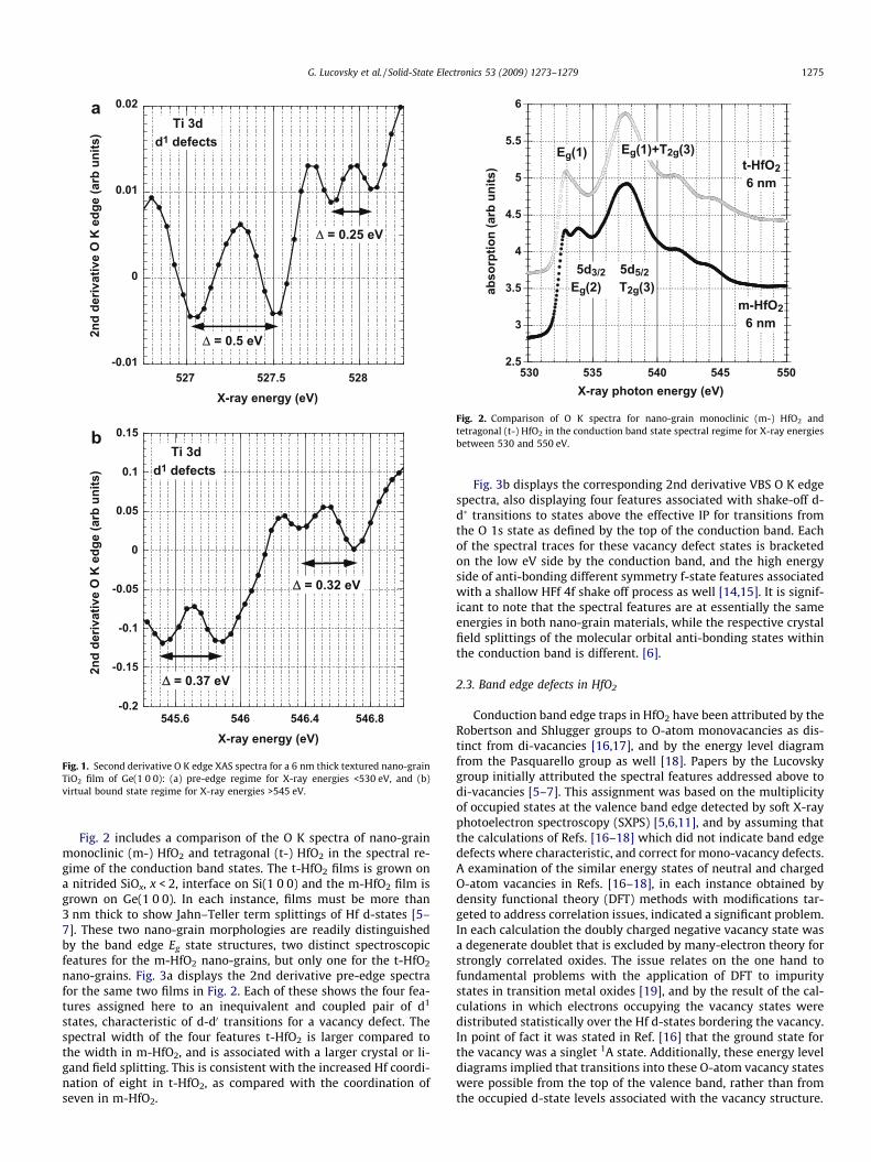
Fig. 2. Comparison of O K spectra for nano-grain monoclinic (m-) HfO2 andtetragonal (t-) HfO2 in the conduction band state spectral regime for X-ray energiesbetween 530 and 550 eV.
G. Lucovsky et al. / Solid-State Electronics 53 (2009) 1273–1279 1275
Fig. 2 includes a comparison of the O K spectra of nano-grainmonoclinic (m-) HfO2 and tetragonal (t-) HfO2 in the spectral re-gime of the conduction band states. The t-HfO2 films is grown ona nitrided SiOx, x < 2, interface on Si(1 0 0) and the m-HfO2 film isgrown on Ge(1 0 0). In each instance, films must be more than3 nm thick to show Jahn–Teller term splittings of Hf d-states [5–7]. These two nano-grain morphologies are readily distinguishedby the band edge Eg state structures, two distinct spectroscopicfeatures for the m-HfO2 nano-grains, but only one for the t-HfO2
nano-grains. Fig. 3a displays the 2nd derivative pre-edge spectrafor the same two films in Fig. 2. Each of these shows the four fea-tures assigned here to an inequivalent and coupled pair of d1
states, characteristic of d-d0 transitions for a vacancy defect. Thespectral width of the four features t-HfO2 is larger compared tothe width in m-HfO2, and is associated with a larger crystal or li-gand field splitting. This is consistent with the increased Hf coordi-nation of eight in t-HfO2, as compared with the coordination ofseven in m-HfO2.
Fig. 3b displays the corresponding 2nd derivative VBS O K edgespectra, also displaying four features associated with shake-off d-d� transitions to states above the effective IP for transitions fromthe O 1s state as defined by the top of the conduction band. Eachof the spectral traces for these vacancy defect states is bracketedon the low eV side by the conduction band, and the high energyside of anti-bonding different symmetry f-state features associatedwith a shallow HFf 4f shake off process as well [14,15]. It is signif-icant to note that the spectral features are at essentially the sameenergies in both nano-grain materials, while the respective crystalfield splittings of the molecular orbital anti-bonding states withinthe conduction band is different. [6].
2.3. Band edge defects in HfO2
Conduction band edge traps in HfO2 have been attributed by theRobertson and Shlugger groups to O-atom monovacancies as dis-tinct from di-vacancies [16,17], and by the energy level diagramfrom the Pasquarello group as well [18]. Papers by the Lucovskygroup initially attributed the spectral features addressed above todi-vacancies [5–7]. This assignment was based on the multiplicityof occupied states at the valence band edge detected by soft X-rayphotoelectron spectroscopy (SXPS) [5,6,11], and by assuming thatthe calculations of Refs. [16–18] which did not indicate band edgedefects where characteristic, and correct for mono-vacancy defects.A examination of the similar energy states of neutral and chargedO-atom vacancies in Refs. [16–18], in each instance obtained bydensity functional theory (DFT) methods with modifications tar-geted to address correlation issues, indicated a significant problem.In each calculation the doubly charged negative vacancy state wasa degenerate doublet that is excluded by many-electron theory forstrongly correlated oxides. The issue relates on the one hand tofundamental problems with the application of DFT to impuritystates in transition metal oxides [19], and by the result of the cal-culations in which electrons occupying the vacancy states weredistributed statistically over the Hf d-states bordering the vacancy.In point of fact it was stated in Ref. [16] that the ground state forthe vacancy was a singlet 1A state. Additionally, these energy leveldiagrams implied that transitions into these O-atom vacancy stateswere possible from the top of the valence band, rather than fromthe occupied d-state levels associated with the vacancy structure.

0
0.02
0.04
0.06
0.08
0.1
529 529.5 530 530.5 531
Hf 5dd1 defects
2nd
deriv
atuv
e XA
S (a
rb u
nits
)
X-ray photon energy (eV)
m-HfO2
t-HfO2
-0.05
0
0.05
0.1
0.15
-0.05
0
0.05
0.1
0.15
546 547 548 549 550 551
Hf 4ff-f*
Hf 5dd1 defects
m-HfO2
t-HfO2
X-ray photon energy (eV)
2nd
deriv
atuv
e XA
S (a
rb u
nits
)
a
b
Fig. 3. Second derivative pre-edge spectra for m-HfO2 and t-HfO2 films in Fig. 2: (a)pre-edge regime for X-ray energies <530 eV, and (b) Schematic representation of d-state orbitals of (a) virtual bound state regime for X-ray energies >545 eV.
0
1
2
3
4
5
6
7
8Hf 5d eg(2)
Hf 5d eg(1)
band gap
SXPSband edge
defects
SE (eV)from VB edge
SE (eV)intra impurity
d-d'
ener
gy re
lativ
e to
top
of v
alen
ce b
and
(eV)
Fig. 4. Initial and final empty states for intra-Hf-atom d-d 0 transitions on the right,and on the left, for transitions originating at the top of the valence band.
1276 G. Lucovsky et al. / Solid-State Electronics 53 (2009) 1273–1279
Fig. 4 is energy level diagram for HfO2 that will be applied to va-cancy defects in HfO2. There is a serious and common misinterpre-tation of spectroscopic ellipsometry features assigned to defecttransitions associated with intrinsic bonding defects, whether theybe mono- or di-vacancies. These are intra-impurity state transitionsas shown in the panel on the right, rather than transitions from thetop of the valence to empty impurity states as suggested in the left-hand panel and obtained by simply inserting the spectroscopictransition energies into an energy band diagram and referencingthem to the top of the valence band. The incorrect assignment onthe left gave final states in the gap that supported the calculationsof the Robertson, Gavartin and Pasquarello groups [16–18], and wasassumed to be correct. However, it did not account for the bandedge trapping discussed in Ref. [20], and this had to be attributedto a different defect state. However when the transition energiesare referenced to the occupied vacancy sites obtained from SXPS,the final states corresponding to the shallow and deep trappingstates reported in electrical measurements are obtained [20]. Thisagreement lends additional support to the energy levels for the cou-pled pair of d1 states as proposed in this paper.
3. Alloy atoms in complex oxides
3.1. Dopant atom electronic states
The incorporation of a tetravalent dopant or alloy atom such asTi for trivalent Sc in normally trivalent GdScO3, forces Ti into a Ti3+
state, producing a d1 electronic structure [2]. This is a general as-pect of substituting a transition metal atom dopant or alloy atomswith a larger number of d-states in their neutral atoms for transi-tion metal (TM) atoms in the complex oxide host. Since both thealloy and host TM atoms must have the same charge state, the sub-stitution for d0 Sc3 by d1 Ti3 changes the GdScO3 d0 host to a d1
complex oxide at the site of the Ti alloy atoms. The Ti for Sc substi-tution satisfies this condition and this results in a singly occupiedTi 3d d1 T2g state above the valence band edge. Whereas vacancydefect concentrations in HfO2 are generally <1019 cm�3, there areessentially no limits of Ti solubility in GdScO3 for a composition re-gime that extends from a doping regime up to 1018–1019 cm�3,well into an alloy regime where the properties of the Gd(Sc,Ti)O3
are modified in a significant way. For example, concentrations ofTi in excess of the local volume percolation threshold of 16–17%with respect to Sc, would be expected to lead to an insulator to me-tal transition with a ferri-magnetic electronic structure, and this isthe discussed in sub-sections 3.2 and 3.4. [21].
3.2. Experimental methods: film deposition and X-ray spectroscopy
Gd(Sc1�xTix)O3 alloys >5 nm thick with x = 0.0, 0.01, 0.05, 0.18and 0.25 were deposited at room temperature in an ultra-high vac-uum system onto (i) LaAlO3 substrates to promote epitaxialgrowth, and onto (ii) superficially oxidized Si(0 0 1) to producenano-grain films. The Ti for Sc substitution results in a Ti3+ ionicstate, and as such the complex oxide is changed from a d0 to a d1
oxide with an occupied Ti T2g state above the valence band edge.Nano-grain dimensions in as-deposited films are <2–2.5 nm, andthe coupling between primitive unit cells is too weak to produceJahn–Teller (J–T) distortions and the subsequent ordering of Tiatoms on the Sc sub-lattice [5,6]. On the other hand, an exchangecorrelation energy for final states can be estimated from the energydifference between the localized Ti band edge alloy atom state andthe first d-state feature of Sc [2]. An insulator to metal transitionfor the alloy single crystal films grown on LaAlO3 and SrTiO3
(STO) substrates films with x = 0.18 and 0.25, a first for intentionaldoping of a d0 complex oxide, GdScO3.

1.6
2
2.4
2.8
3.2
528 530 532 534 536 538 540
O K
edg
e XA
S ab
sorp
tion
(arb
. uni
ts)
Sc 3dT2g Eg
Gd 12-states6s, 6p, 5d, 5f
Ti 3dT2g
Gd(Sc0.75Ti0.25)O3solid dots epitaxial film
distorted cubic perovskiteopen circles
as-deposited nano-grain film X-ray amorphous
X-ray photon (energy)
Fig. 6. XAS O K edge spectral for Gd(Sc0.75,Ti0.25)O3 alloy films. Highlighted are theTi 3d T2g feature in the pre-edge regime <531 eV, Sc 3d T2g and Eg features centeredat �532 eV, and Gd molecular orbital features centered at �535 eV. Solid dots arefor an epitaxial film, and open dots for abas-deposited X-ray amorphous film on anSi.
G. Lucovsky et al. / Solid-State Electronics 53 (2009) 1273–1279 1277
The crystal structure in the epitaxial films does not requireannealing to promote chemical ordering of the Ti atoms on theSc sub-lattice sites, and this results in an insulator to metal transi-tion in these as-deposited films for the x = 0.18 and 0.25 alloysfilms. This transition has been confirmed directly by electricalmeasurements. The same transition has been confirmed by a novelapplication of X-ray absorption spectroscopy, XAS, using numericalintegration of O K edge spectra that extends into the in the pre-edge, and vacuum continuum regimes for X-ray energies<530 eV, and >545 eV, respectively.
3.3. X-ray spectra and data reduction
Fig. 5 displays O K edge spectra for the epitaxial films that intro-duces a novel way to detect the insulator to metal transition. Highlevels of charging in the insulating films, x = 0.0, x = 0.01 andx = 0.05 reduce the signal level by more than factor of 30 with re-spect to substantially higher signal levels with no evidence forcharging in the metallic films with x = 0.18 and 0.25. The total en-ergy yield, TEY, detection method relies on current flow throughthe surface of the epitaxial film to balance positive charge associ-ated with photoelectron emission during X-ray irradiation, so thatit can easily distinguish between insulating and metallic films.
The significant aspect of the O K edge spectra in Fig. 6 is relatedto the insulator to metal transition that reveals differences be-tween the energy of the Ti defect/alloy atom state for the 0.25 al-loys that are (i) epitaxial films on an STO substrate, and (ii) as-deposited nano-grain films on oxidized Si substrates. The energydifference between the Ti alloy atom states and the lowest energyT2g band edge states is deeper in the gap and shifted to lower en-ergy by �1 eV with respect to the Ti alloy atom defect in the X-rayamorphous film.
This energy difference is also revealed in the second derivativeO K edge spectra in Fig. 7a and b, for two different spectral regimesthat include the pre-edge and conduction band energy regimes.These are 528–539 eV in Fig. 7a, and 528–532 eV in Fig. 7b. Con-sider first the spectra in Fig. 7(a) in the conduction band regime be-tween �531 eV and 539 eV. These spectra compare the epitaxialfilms with the nano-grain films in samples that have been annealed
0.1
1
530 535 540 545
film charginginsulator to
metal transition
5% Ti 95% Sc
18% Ti 82% Sc
25% Ti 75% Sc
Gd(Sc,Ti)O3 onLaAlO3
X-ray photon energy (eV)
log
10 a
bsor
ptio
n (a
rb u
nits
)
Fig. 5. XAS O K ege spectra of epitaxial Gd(Sc1�x,Tix)O3 alloys on STO substrates.Films are sufficiently thick so that there are no spectral features due to X-rayabsorption in the substrate. Spectra are for films with different Ti concentration: aninsulating film with x = 0.05 (5%), and two metallic films with x = 0.18 (18%) and0.25 (25%).
to 900 �C. The Gd atoms are in a distorted six fold coordinated site,and the Gd atoms in a 12-fold coordinated and distorted environ-ment as well. The O atoms are six fold coordinated with two differ-ent bond lengths for the Sc and Gd neighbors. Grain growth inthese annealed nano-grain films is sufficient to reveal the Jan–Tell-er term splittings in the Eg feature in the nano-grain film [5,6],whereas these splittings are readily evident in the epitaxial films.Specifically, the Sc 3d T2g and Eg, triplet and doublet multipletsare completely resolved in the epitaxial film whereas, the T2g trip-let is better resolved in the nano-grain film. These term splitting ofthe T2g state is consistent with the band edge p-bonding, and Eg
doublet splitting with one component of the r-bonding which alsoincludes Sc 4s and 4p states that overlap the features associatedthe twelve Gd r-bonding states, which includes a mix of Gd 6s,6p, 5d and 5f states. We will not attempt to deconvolve the spectrafeatures between 533 and 539 eV that include a mix of Sc 4s and 4pstates and the twelve Gd r-bonding states as well. Instead the fo-cus will be on the Ti alloy states at the band edge.
Moving onto the second derivative XAS spectra in Fig. 7(b),which display the pre-edge region as well as the Sc T2g states. Con-sider first the annealed nano-grain spectrum for the alloy with 25%Ti and 75% Sc, and focus on the second derivative minima at�529.8 eV. The first point is indicated by the lower arrow, labeled‘‘1”. This indicates the energy difference, of �1 eV between the Tiimpurity level and the Sc T2g feature that has been already notedin Fig. 6. The value of 1 eV is a final state correlation energy, butfrom the perspective of the transition energies for excitation ofelectrons out of occupied states, rather than a spectroscopicallydetermined energy difference between occupied spin states with‘‘up” and ‘‘down” character [2]. This energy difference is addressedin Fig. 8, which displays the SXPS spectrum of the epitaxial film.
Returning to Fig. 7b. the upper arrow, labeled ‘‘2” indicates theenergy difference between the strongly correlated spin band atlower eV, and the weaker opposite spin band in the epitaxial film.This energy difference is also �1 eV, and the energy difference be-tween the average of this two bands coincides with the position ofthe center correlation energy defined by the difference in energybetween the occupied alloy atom state and the lowest energy T2g
Sc d-state. The equality of these two energy differences, each of

-0.004
-0.003
-0.002
-0.001
0
0.001
0.002
528 530 532 534 536 538
O K
XA
S 2n
d de
rivat
ive
X-ray photon energy (eV)
Ti 3dT2g
Sc 3dT2g Eg
solid dots epitaxial filmdistorted cubic perovskite
open circles nano-grain film
Gd(Sc0.75Ti0.25)O3Gd 12-states6s, 6p, 5d, 5f
1
2
-0.004
-0.0032
-0.0024
-0.0016
-0.0008
0
0.0008
0.0016
0.0024
528 529 530 531 532 533-0.004
-0.0032
-0.0024
-0.0016
-0.0008
0
0.0008
0.0016
0.0024
O K
XA
S 2n
d de
rivat
ive
X-ray photon energy (eV)
Ti 3dd1
Sc 3dT2g
solid dots epitaxial filmdistorted cubic perovskite
open circles nano-grain film
Gd(Sc0.75Ti0.25)O3
o
o
oo
spin bands
a
b
Fig. 7. Second derivative XAS O K edge spectra for the x = 0.25, Gd(Sc0.75,Ti0.25)O3
alloy conduction band and band edge defects states. Arrows 1 and 2 indicaterespectively a transition exchange correlation energy: (1) between the energy of theTi 3d defect state and the lowest Sc 3d T2g state, and (2) between the energy of acorrelated majority spin band at �529.5 eV and the minority spin band at 531 eV:(a) in the spectral range from 528 eV to 539 eV, and (b) from 528 eV to 532 eV.
0
5000
1 10 4
1.5 10 4
2 10 4
2.5 10 4
3 10 4
3.5 10 4
4 10 4
612 614 616 618 620 622 624 626
coun
ting
rate
(arb
uni
ts)
electron kinetic energy (eV)
Gd(Sc,Ti)O3 onLaAlO3
25% Ti 75% Sc
Ti T2goccupied
strongly correlatedspin band
Fermi levelabove band edge
Sc and O molecular orbital
valence band states
Fig. 8. SXPS valence band spectrum for the x = 0.25, Gd(Sc0.75,Ti0.25)O3 alloyepitaxial film. The occupied Ti2g strongly correlated spin band feature and theFermi level are marked with arrows.
1278 G. Lucovsky et al. / Solid-State Electronics 53 (2009) 1273–1279
which is equal to an effective exchange correlation energy, is dis-cussed in the next section, and its very existence is an importantconsequence of the double exchange mechanism for ferro-, or fer-ri-magnetism which may be present in these films [21].
Another important aspect of the 25% Ti alloy epitaxial film, thatis also evident in the 18% Ti alloy film, is the energy difference be-tween the Ti 3d strongly correlated spin state band and the Fermilevel. This is indicated in the SXPS spectrum in Fig. 8. The Ti 3d cor-related spin band at �616 eV and is below the Fermi level at�621 eV, and this is a characteristic signature of ferro- or ferri-mag-netic behavior in general, and therefore present in metal films, aswell as in complex oxides of this article in which there is an insu-lator to metal transition [2]. This energy difference is about twotimes the T2g–Eg crystal field (C-F) splitting for TiO2, and for octa-hedral complexes in general [2,5,6]. It is important to note that
the Fermi level position in the GdScO3 host is determined by theoccupied 4f states of Gd, whereas the edge of the valence band iscloser to 618 eV.
3.4. The insulator to metal transition
There are two different mechanisms for coupling of electronspins for occupied dn, n > 1 transition metal atoms in TM elementaland complex oxides. The super exchange mechanism prevails inmost dn TM elemental oxides, with n P 1, and is which may bepresent in these films based on the inherent symmetry of TM dp– O atom pp – TM dp coupling or equivalently, TM dr – O atompr – TM dr coupling. This produces a d-p-d generic symmetrydetermined anti-ferromagnetism in the vast majority of first rowTM elementals [22]. There are at least two noteworthy exceptions:CrO2, and the mixed valence oxide Fe3O4. A double exchangemechanism prevails in the mixed valence oxide Fe3O4. This derivesfrom a homogeneous alloy mixture of FeO and Fe2O3 with formallydivalent and trivalent Fe, respectively [2]. A similar mechanismalso prevails in CrO2, but the quantitative and qualitative aspectsof the magnetic behavior are different [23].
The objective of the research described in this part of the articleis to demonstrate that the insulator–metal transition required forthe double exchange mechanism could be achieved in an ‘‘intelli-gently-designed” complex oxide and detected spectroscopicallyas well. The double exchange mechanism is dynamic and basedon many-body theory in which the metallic state is a mixture ofmultiple ionic states with different formal valence [2,21]. The alloysystem that we have chosen was anticipated to have an insulatorto metal transition when the concentration of Ti3+ on the Sc sub-lattice exceeded a volume percolation threshold of 16% [24]. Themeans that the occupied Ti d-states in the d1 configuration experi-ence a substantial degree of connectedness so that a strongly cor-related spin up (or spin down) band is generated. This is indeed thecase as illustrated in the spectra in Figs. 7 and 8. The magnitude ofthe exchange correlation energy determines whether ferro- or fer-ri-magnetic behavior prevails. In this system that energy is �1 eV,and comparable to width of the occupied strongly correlated spinband, so that ferri-, rather than ferro-magnetism prevails.
Summarizing the results presented in Section 3. Nano-grain andepitaxial thin films of Gd(Sc1�xTix)O3 alloys >5 nm thick with

G. Lucovsky et al. / Solid-State Electronics 53 (2009) 1273–1279 1279
x = 0.0, 0.01, 0.05, 0.18 and 0.25 have been prepared and studied byXAS and XPES. These studies have identified an insulator to metaltransition for films with x = 0.18 and 0.25, consistent with astrongly correlated Ti 3d state metallic conductivity band. Futurestudies will oxides, and combine XAS, XPES spectroscopic studieswith electrical and magnetic measurements as well, and be ex-tended to other alloys in which dn states with n > 1 result.
4. Discussion: strongly correlated transition metal states:intrinsic bonding defect in HfO2 and Ti d1 states in GdSc1�xTixO3
As already note, it has been recognized for at least ten years thatthe ultimate limits of Si device scaling with increased performanceand functionality require the replacement of thermally grown anddeposited SiO2 and Si oxynitride alloy gate dielectrics with transi-tion metal oxides and silicates with higher dielectric constants [1].Higher dielectric constants allow the use of physically thicker filmsfor the required levels of dielectric capacitance while at the sametime maintaining tunneling leakage currents that do not degradedevice performance. Therefore it is important to understand bothexperimentally, and theoretically, science base differences be-tween defect and band edge states in SiO2 and transition metal oxi-des and silicates. This has been addressed in Section 2, where thesedifferences were demonstrated by a mix of spectroscopic methods,and explained in the context of many-electron theory [2].
In addition to extending the performance of gate dielectrics be-low an equivalent oxide thickness of 1–1.5 nm, and thereforerequiring high-k transition metal dielectrics, there has been alsoa desire to increase chip functionality, e.g., by introducing ferro-magnetic and ferroelectric thin film layers [2], and in particularmultiferroic materials in which there are opportunities for noveldevice configurations with coupled magnetic and ferroelectricfunctionality [3]. This article has demonstrated in Section 3 thatan insulator to metal transition can be introduced into a d0 com-plex oxide, GdScO3, by introduction of a normally tetravalent tran-sition metal, Ti, onto trivalent Sc sites, thereby creating a d1
electron state for each substituted Ti atom.The spectroscopic studies reported in Sections 2 and 3 have
demonstrated the importance of occupied TM atoms in under-standing limitations in one case, the electronic structure of vacancydefects in HfO2, and opportunities in another, the introduction of ainsulator to metal transition by alloying into a normally insulatingand non-magnetic complex oxide, GdScO3.
The electronic structures associated with the vacancy defects,and the alloy substitution discussed in Sections 2 and 3 could onlybe explained by using a theory that applies to strongly correlatedsystems [2,4,8,19], and is different in many important qualitativeways that the theories have addressed SiO2 gate dielectrics, andthe Si–SiO2 interface. This requires the development of a new par-adigm that takes into account differences between this challenge,and in particular recognizing that many of the theoretical andexperimental approaches that have underpinned the evolution ofSi devices with SiO2 and Si oxynitride dielectrics, and poly-Silicongate electrodes do not apply for transitional metal oxides and sili-cates, and ferroelectric and ferro-magnetic complex oxides.
Note added in proof
This note presents an additional example of how interpretationof spectroscopic data using many-electron theory provides signifi-cant insights into the electronic states in complex oxides. Experi-mental verification of mixed valency has been obtained bycomparing O K edge spectra of LaMnO3 and La0.8Sr0.2MnO3. Newlyobtained XAS O K edge spectra have indicated changes characteris-tic of an insulator to metal transition for the 20% Sr for La atom
substitution, as well as mixed valency. These include (i) a changefrom a distorted perovskite structure in LaMnO3 to a cubic perov-skite in La0.8Sr0.2MnO3, (ii) pre-edge shake-up, and vacuum contin-uum shake-off features consistent with the d4 character of Mn3+ inLaMnO3, and (iii) additional sharp features in the shake-up andshake-off regimes in La0.8Sr0.2MnO3 consistent with the d3 charac-ter of the Mn4+. Additionally, These spectral changes confirm thatEg symmetry electron of the d4 configuration contributes to themetallic conductivity consistent with a schematic representationof double exchange by Cox in Ref. [2]. The mixed valency is alsoconfirmed by the multiplicity and relative energies of features inthe MnL2,3 specturm.
La0.8Sr0.2MnO3 alloy and Fe3O4 are examples for the double ex-change mechanism applied to La1-xCaxMnO3 by De Gennes [21] andproposed originally by Zener [22]. This mechanism predicts the rel-ative ease of electron exchange between two transition metal dn,n>1 ion states, each with different values of n, such as Mn3+ d4
and Mn4+ d3 in La0.8Sr0.2MnO3. The mechanism relies on electrontransport in which the exchanged electron does not change spin,preserving the Hund’s rule occupancy that is crucial for ferromag-netism. This leads to ferromagnetic alignment in La0.8Sr0.2MnO3,where metallic behavior results from the Sr concentration of 20%exceeding a percolation threshold, �17% [23].
Whereas double exchange mechanism relies on mixed valencyto promote ferromagnetic behavior, not all mixed valence materi-als display double exchange and/or ferromagnetism [24,25]. Ferro-magnetism in La1-xCaxMnO3 alloys, which are isolectronic analogsof La1-xSrxMnO3, is dependent on both composition, x, and temper-ature, demonstrating that additional factors are important for thiscooperative behavior.
There is no spectroscopic evidence for mixed valency inGdSc0.75Ti0.25O3 alloy of this article. This has been established byrecently obtained L2,3 spectra which confirm the d1 configurationfor substituted Ti3+, and the d0 configuration for host Sc3+. It unli-kely that a double exchange process would derive from a mixingof the Ti d1 state with occupied Gd f7 states.
References
[1] Houssa M, Hyens MM. in: Houssa M, editor, High-k gate dielectrics. Bristol:Institute of Physics; 2004 [Chapter 1.1].
[2] Cox PA, Transition metal oxides. Oxford: Clarendon; 1992 [chapters 2, 3 and 5].[3] Cheong S-W, Mostovoy M. Nat Mater 2007;6:13.[4] Cotton FA. Chemical applications of group theory. 2nd ed. New York: Wiley
Interscience; 1963 [chapter 8].[5] Lucovsky G, Seo H, Lee S, et al. Japan J Appl Phys 2007;46:1899.[6] Lucovsky G. J Mol Struct 2007;838:187.[7] Lucovsky G et al. Microelectron Eng 2009;86:1676.[8] de Grott F, Kotani A. Core level spectroscopy of solids. Boca Ratan: CRC Press;
2008 [chapter 4].[9] Condon EU, Shortley GH. The theory of atomic spectra. London: Cambridge
University Press; 1957 [chapters VI–X].[10] Harrison WA. Elementary electronic structure. Singapore: World Scientific;
1999.[11] Koiller B, Falicov LM. J Phys C: Solid State Phys 1974;7:299.[12] Fleming L et al. J Appl Phys 2007;120:033707.[13] Lucovsky G et al. Microelectron Eng 2007;84:2350.[14] Teo BK. EXAFS: basic principles and data analysis. Berlin: Springer Verlag;
1986 [chapter 5].[15] Stöhr J. NEXAFS spectroscopy. Berlin: Springer; 2003 [chapters 2 and 4].[16] Xiong K, Robertson J, et al. Appl Phys Lett 2005;87:183505 [and reference
therein].[17] Gavartin JL, Ramo DM, et al. Appl Phys Lett 2006;89:082908 [and reference
therein].[18] Broqvista P, Pasquarello A. Appl Phys Lett 2006;89:262904.[19] Bersuker IB. J. Comput Chem 1997;18:260.[20] Autran JL, et al. In: Houssa M, editor, High-k gate dielectrics. Bristol: Institute
of Physics; 2004 [chapter 3.4].[21] DeGennes PG. Phys Rev 1960;118:141.[22] White RM, Geballe TH. Long range order in solids, solid state physics
supplement 15. New York: Academic Press; 1979 [chapter IV].[23] Scher H, Zallen R. J Chem Phys 1970;53:3759.[24] Korotin MA, Anisimov VI, Khomskii DI, et al. Phys Rev Lett 1998;80:4305.[25] Varma CM. Rev Modern Phys 1976;42:219.
%d0%9f%d0%be%d0%bb%d0%be%d0%b6%d0%b5%d0%bd%d0%b8%d0%b5 %d0%9f%d0%be%d1%81%d0%bb%d1%8b%20%d0%9f%d0%be
%d0%bf%d1%80%d0%be%d0%b5%d0%ba%d1%82%d0%b8%d1%80%d0%be%d0%b2%d0%b0%d0%bd%d0%b8%d0%b5 %d0%b2%d0%bd%d1
%d0%93%d0%a3%d0%97%20%d0%93%d0%b0%d0%b7 %d0%97%d0%b0%d0%b2%d0%be%d0%b4%d1%81%d0%ba%d0%b0%d1%8f%20%d0
%d0%a4%d0%93%d0%9e%d0%a1%203 %20%d0%9b%d0%b5%d1%87%d0%b5%d0%b1%d0%bd%d0%be%d0%b5%20%d0%b4%d0%b5%d0%b
%d0%a1%d0%b1%d0%be%d1%80%d0%bd%d0%b8%d0%ba %d0%a1%d1%8a%d0%b5%d0%b7%d0%b4%d0%a2%d0%b5%d1%80%d0%b0%d0
%d0%b5 %d0%b5%d0%ba%d1%80%d0%b0%d0%bd %d0%b4%d0%be%d1%80%d0%b0%d0%bd%d0%b8%d0%ba%d0%b8 %d0%bb%d1%8e%
%d0%a3%d1%87%d0%b5%d0%b1%d0%bd%d1%8b%d0%b9%d0%9f%d0%bb%d0%b0%d0%bd %d0%a4%d1%83%d0%bd%d0%b4%d0%9c%d0
%d0%a3%d1%87%d0%b5%d0%b1%d0%bd%d0%b8%d0%ba%d0%b8%20%d0%98%d0%b7%d0%b4 %d0%b2%d0%b0%20%d0%9c%d0%98%d0
%d0%9a%d0%b0%d1%82%d0%b0%d0%bb%d0%be%d0%b3 %d0%9c%d0%be%d0%bb %d0%a1%d0%bf%d0%b5%d1%86 %d1%83%d0%ba%