co- manager nepp program ://nepp.nasa.gov/files/25522/neppetw2010_label_theview10k.pdf · in the...
TRANSCRIPT
The View from 10,000 ft –what is happening and what it means for
flight electronics
Co- Manager NEPP Program
http://nepp.nasa.gov
Kenneth A. [email protected]
301-286-9936
1The View from 10,000 Feet presented by Kenneth A. LaBel at NEPP ETW, NASA/GSFC – June 22, 2010

Outline• What’s New with
Electronics• What’s Unique About
Space and Electronics• How is NEPP
Approaching the Problem
2The View from 10,000 Feet presented by Kenneth A. LaBel at NEPP ETW, NASA/GSFC – June 22, 2010
Atomic Interactions– Direct Ionization
–http://www.stsci.edu/hst/nicmos/performance/anomalies/bigcr.html
Interaction with Nucleus– Indirect Ionization– Nucleus is Displaced

The Amazing Progression of the Integrated Circuit (IC)
• We have been eyewitnesses to the revolution that’s taken place in the semiconductor industry– What was once inconceivable is now
the ordinary• Several factors have been at the
forefront of this movement– Integration
• Increasing functionality in decreased space
– Material science• Using science to modify the silicon
transistor and it’s package
3The View from 10,000 Feet presented by Kenneth A. LaBel at NEPP ETW, NASA/GSFC – June 22, 2010
Inside a Apple iPhone™ player
Note: this talk has a bit more radiation focus than reliability due to my background

4
The Growth in IC Availability• The semiconductor industry has seen an explosion in the
types and complexity of devices that are available over the last several decades– The commercial market drives features
• High density (memories)• High performance (processors)• Upgrade capability and time-to-market (FPGAs)• Wireless (RF and mixed signal)
• Long battery life (Low-power CMOS)
Zilog Z80 Processorcirca 1978
8-bit processorIntel 65nm Dual Core Pentium D Processor
circa 2007Dual 64-bit processors
Integrated Cycling Biband MP3

5
Types of Electronic Parts for Space
• One may view electronic parts for space as meeting needs in three categories– Standard electronics
• E.g., capacitors– Basic components
– Standard building blocks• E.g., Field Programmable Gate Arrays (FPGAs)
– Widespread usage in most systems
– Custom devices not available as “off-the-shelf”• E.g., nuclear power or EVA
– Needed for a specific application - ASIC
• Note: Commercial-of-the-shelf (COTS) assemblies (e.g., commercial electronic cards or instruments) also may be considered– Screening is more complicated than ever
before!
ACTEL RTSX72S FPGAA part that passed “standard”
qualification, but requiresmore complex testing
The View from 10,000 Feet presented by Kenneth A. LaBel at NEPP ETW, NASA/GSFC – June 22, 2010

6
A Critical Juncture for Space Usage –Commercial Changes in the Electronics World
• Scaling of technology– Increased gate/cell density per unit area (as well as power and
thermal densities)– Changes in power supply and logic voltages (<1V)
• Reduced electrical margins within a single IC
– Increased device complexity, # of gates, and hidden features– Speeds to >> GHz (CMOS, SiGe, InP…)
• Changes in materials– Use of antifuse structures, phase-change materials, alternative K
dielectrics, Cu interconnects (previous – Al), insulating substrates, ultra-thin oxides, etc…
• Increased input/output (I/O) in packaging
– Use of flip-chip, area array packages, etc
• Increased importance of application specific usage to reliability/radiation performance
The View from 10,000 Feet presented by Kenneth A. LaBel at NEPP ETW, NASA/GSFC – June 22, 2010

7
The Changes in Device Technology• Besides increased availability, many changes have taken
place in– Base technology,– Device features, and,– Packaging
• The table below highlights a few selected changes

8The View from 10,000 Feet presented by Kenneth A. LaBel at NEPP ETW, NASA/GSFC – June 22, 2010

What is a Scaled CMOS anyway?
• It’s all about transistors and sizing (known as gate or channel lengths) and the desire to pack as many transistors on a chip as possible– Transistor node space is now commercially at 32nm
(and 25nm is sampling!)
9The View from 10,000 Feet presented by Kenneth A. LaBel at NEPP ETW, NASA/GSFC – June 22, 2010

Package Complexity - Evolution
10The View from 10,000 Feet presented by Kenneth A. LaBel at NEPP ETW, NASA/GSFC – June 22, 2010
Dual in-line Package (DIP)10’s of pins
Wirebonded, through hole
Quad Flatpack (QFP)100’s of pins
Wirebonded, surface mount
Area Array Package1000’s of pinsBump bonded,
surface mount or columns added

11
The Challenge for Selecting ICs for Space• Considerations since
the “old days”– High reliability (and
radiation tolerant) devices
• Now a very small market percentage
– Commercial “upscreening”
• Increasing in importance• Measures reliability,
does not enhance– System level
performance and risk• Hardened “systems” not
devices
ASICs?
FPGAs?
Processor?DSPs
Flash?
SDRAM?
System DesignerTrying to meet high-resolution instrument requirements AND
long-life in a space environemnt
SerDes?ADCs?
The View from 10,000 Feet presented by Kenneth A. LaBel at NEPP ETW, NASA/GSFC – June 22, 2010

12
Microelectronics: Categories• Microelectronics can be viewed several ways
– Digital, analog, mixed signal, other– Complementary Metal Oxide Semiconductor (CMOS), Bipolar, etc...– Function (microprocessor, memory, …)
• There are only two commercial foundries (where they build devices) in the US dedicated to building radiation hardened digital devices. Several others have “foundryless” options.
– Efforts within DoD to provide alternate means of developing hardened devices
• Hardened-by-design (HBD)• Provides path for custom devices, but not necessarily off-the-shelf devices
– Commercial devices can have great variance in radiation tolerance from device-to-device and even on multiple samples of same device
• No guarantees!– Analog foundry situation is even worse
• New technologies have many unknowns– Ultra-high speed, nanotechnologies, microelectromechanical systems
(MEMS and the optical versions – MOEMS), …
A MOEMS in action
The View from 10,000 Feet presented by Kenneth A. LaBel at NEPP ETW, NASA/GSFC – June 22, 2010

NEPP:If we used strictly commercial parts
• NEPP is the only entity at NASA that– Trains young engineers in the difference and provides a growth path
for developing project parts and radiation engineers– Develops and validates qualification methods– Provides knowledge that allows insertion of modern devices into our
space systems– Shares and gathers knowledge with all the industry
• If the flight projects don’t know there’s a problem…13
Terrestrial Space
Lifetime 1-3 years, then replaced or thrown out
1-20 years and rarely replaceable
Thermal 0-70C -55 to +125C with extremes much higher and lower
Shock Oops! I dropped it. Time to get an upgrade anyway…
Launch vibration
Anomaly Reboot or power cycle or return to dealer
Anomaly or failure
Radiation Is the microwave on? Protons, electrons, cosmic rays, …
The View from 10,000 Feet presented by Kenneth A. LaBel at NEPP ETW, NASA/GSFC – June 22, 2010

14
Space Environments and Related Effects
Plasma
Charging ImpactsDrag SurfaceErosion
Ultraviolet & X-ray
Neutralgas particles
Particleradiation
Micro-meteoroids & orbital debris
Ionizing &Non-IonizingDose
•Degradation of micro-•electronics•Degradation of optical components•Degradation of solar cells
SingleEventEffects
•Data corruption•Noise on Images•System shutdowns•Circuit damage
•Degradation of thermal, electrical, optical properties•Degradation of structural integrity
•Biasing of instrument readings•Pulsing•Power drains•Physical damage
•Torques•Orbital decay
•Structural damage•Decompression
–Space Radiation Effectsafter Barth
The View from 10,000 Feet presented by Kenneth A. LaBel at NEPP ETW, NASA/GSFC – June 22, 2010

15
Space Radiation Environment
Trapped ParticlesProtons, Electrons, Heavy Ions
afterNikkei Science, Inc.of Japan, by K. Endo
Galactic Cosmic Rays (GCRs)
Solar Protons&Heavier Ions
Deep-space missions may also see: neutrons from backgroundor radioisotope thermal generators (RTGs) or other nuclear sourceAtmosphere and terrestrial may see GCR and secondaries
The View from 10,000 Feet presented by Kenneth A. LaBel at NEPP ETW, NASA/GSFC – June 22, 2010

16
Implications for Electronics in Space• With all these changes in the
semiconductor world, what are the implications for usage in space? Implications for test, usage, qualification and more
– Speed, power, thermal, packaging, geometry, materials, and fault/failure isolation are just a few for emerging challenges for radiation test and modeling.
• Reliability challenges are equally as great
– The following chart (courtesy of Vanderbilt University) looks at some of the recent examples of test data that imply shortfalls in existing radiation performance models.
• Technology assumptions in standard tools such as CREME96 are no longer valid
Global
Intermediate
Metal 1
Passivation
DielectricEtch Stop Layer
Dielectric Capping LayerCopper Conductor with Barrier/Nucleation Layer
Pre-Metal Dielectric
Metal 1 Pitch
Tungsten Contact Plug
Via
Wire
Global
Intermediate
Metal 1
Passivation
DielectricEtch Stop Layer
Dielectric Capping LayerCopper Conductor with Barrier/Nucleation Layer
Pre-Metal Dielectric
Metal 1 Pitch
Tungsten Contact Plug
Via
Wire
Typical device cross-section.Current generations of digital devices
take over 1500 processing steps.
The View from 10,000 Feet presented by Kenneth A. LaBel at NEPP ETW, NASA/GSFC – June 22, 2010

17
Sample Radiation Modeling Shortfalls
Reed-05
The View from 10,000 Feet presented by Kenneth A. LaBel at NEPP ETW, NASA/GSFC – June 22, 2010

18
Where we are –Radiation test methods and what has changed in
the world• Existing test methods
– SEE• JEDEC JSD 57• ASTM, F1192-00
– TID• MIL-STD-883B, Test Method
1019.8• ASTM, F1892-06
• All had prime development in the mid-90s with some updates since, however, many new issues have been discovered that may not be covered adequately
• Examples: Recent SEE Phenomena
– Angular effects in SOI technologies
– Role of single event transients (SETs) and commensurate speed-related issues in both analog and digital circuits
– Ion penetration and range issues in power and packaged components
– Approaches to die access– Impact of application and
reconfigurable approaches to SEE performance
– Role of nuclear reactions from heavy ion particle interactions
1.E-151.E-141.E-131.E-121.E-111.E-101.E-091.E-081.E-07
0 20 40 60 80 100
LET (MeV*cm2/mg)
Cro
ss S
ectio
n (c
m2 /bit)
T=125CVDD=3.1V=0º
Courtesy ISDE, Vanderbilt University
Reliability testing has had commensurate complications
The View from 10,000 Feet presented by Kenneth A. LaBel at NEPP ETW, NASA/GSFC – June 22, 2010

19
Hypothetical New Technology Part Qualification Cost Circa 2008
Item Cost Note
Parts Procurement(500-1000 devices for
testing only)
$25-1000K Individual device costs can run from cents to tens of thousands
“Standard” Qualification Tests
$300K
Radiation Tests and Modeling
$400K Assumes total dose and single event (heavy ion) only
Failure Modes Analysis $300K Out-of-the-box look at the “hows and whats” for non-standard
research required for qualification
Additional Tests, Modeling, and Analysis based on Failure Modes
$500K
Total cost for one device type
$1.5-3M Not all new technologies will meet standard qualification
levels: technology limitations document
Assumption: 12-24 months to develop sufficient data for technology confidence

20
Device Complexity Drives Cost and Schedule!- Ex., Standard Memory
2006 SEE Test of SDRAM
Description
Man-weeks or units Cost in $ Total Note
Heavy Ion at TAMU
Test plan 1.00 $4,000.00 $4,000.00
Includes eng, rad, other to define what needs to go into test set with project.
Device procurements 10.00 $75.00 $750.00Misc parts 1.00 $1,000.00 $1,000.00 Higher speed drives cost
Device thinning and package processing 10.00 $350.00 $3,500.00
Assumes FBGA package; If this does not work, more expensive test facility like NSCL needed: >$100K delta
Daughterboard Board design - electrical 0.40 $4,000.00 $1,600.00Daughterboard Board design - PCB 0.50 $3,500.00 $1,750.00Test Boards 10.00 $500.00 $5,000.00Board population 0.40 $3,500.00 $1,400.00Board/tester debug 0.50 $4,000.00 $2,000.00Tester VHDL development 3.00 $4,000.00 $12,000.00Technician 1.00 $3,500.00 $3,500.00Rad expert (test oversight and plan) 0.60 $5,000.00 $3,000.00Heavy ion test performance - contractor 2.00 $2,000.00 $4,000.00
TAMU 16.00 $750.00 $12,000.00
2X time required: more data, more error types, more complex results
Data analysis 3.00 $3,500.00 $10,500.00Test report (eng, rad expert, rad lead) 1.00 $4,000.00 $4,000.00
Total in $70,000.00
1996 SEE Test of a 4M SRAM
Description
Man-weeks or units Cost in $ Total Note
Heavy Ion at BNL SEUTF
Test plan 0.20 $4,000.00 $800.00
Includes eng, rad, other to define what needs to go into test set with project.
Device procurements 10.00 $50.00 $500.00Misc parts 1.00 $250.00 $250.00 Sockets, connectors, etc...Device delidding 0.05 $3,500.00 $175.00Test board design - electrical and layout 0.40 $4,000.00 $1,600.00Board fab and population 1.00 $3,500.00 $3,500.00 In-house board buildBoard/tester debug 0.50 $4,000.00 $2,000.00Rad expert (test oversight and plan) 0.40 $5,000.00 $2,000.00Heavy ion test performance - contractor 2.00 $1,500.00 $3,000.00BNL Beam 6.00 $700.00 $4,200.00 Simple data: bit flips, latchupData analysis 1.00 $3,500.00 $3,500.00Test report (eng, rad expert, rad lead) 0.50 $4,000.00 $2,000.00
Total: $23,525.00
Other test costs (radiation and reliability)have increased commensurately with ~3X schedule increase as well!
1996 vs 2006 a 3X Cost Delta
Now >> $100KThe View from 10,000 Feet presented by Kenneth A. LaBel at NEPP ETW, NASA/GSFC – June 22, 2010

NEPP Mission
• To provide guidance to NASA: – Selection and application of
microelectronics technologies– Improved understanding of risks
related to the use of these technologies in the space environment
– Appropriate evaluations to meet NASA mission assurance needs for electronic systems
• NEPP evaluates new* and emerging** electronic parts technologies and provides assurance support for technologies in current use in NASA spaceflight systems *New – Recently marketed, commercially available
** Emerging – Available in limited quantities for evaluation, on path to commercial products
21The View from 10,000 Feet presented by Kenneth A. LaBel at NEPP ETW, NASA/GSFC – June 22, 2010

22
NEPP Overview• NEPP supports all of NASA for >20 years
– 7 NASA Centers and JPL actively participate• The NEPP Program focuses on the reliability aspects of
electronic devices– Three prime technical areas: Parts (die), Packaging, and Radiation
• Alternately, reliability may be viewed as:– Lifetime, inherent failure and design issues related to the
electronic parts technology and packaging, – Effects of space radiation and the space environment on these
technologies, and– Creation and maintenance of the assurance support
infrastructure required for mission success.
Electrical overstress failurein a commercial electronic device
The View from 10,000 Feet presented by Kenneth A. LaBel at NEPP ETW, NASA/GSFC – June 22, 2010
23
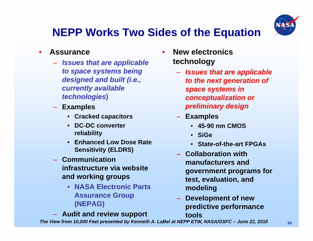
NEPP Works Two Sides of the Equation• Assurance
– Issues that are applicable to space systems being designed and built (i.e., currently available technologies)
– Examples• Cracked capacitors• DC-DC converter
reliability• Enhanced Low Dose Rate
Sensitivity (ELDRS)– Communication
infrastructure via website and working groups
• NASA Electronic Parts Assurance Group (NEPAG)
– Audit and review support
• New electronics technology– Issues that are applicable
to the next generation of space systems in conceptualization or preliminary design
– Examples• 45-90 nm CMOS• SiGe• State-of-the-art FPGAs
– Collaboration with manufacturers and government programs for test, evaluation, and modeling
– Development of new predictive performance tools
The View from 10,000 Feet presented by Kenneth A. LaBel at NEPP ETW, NASA/GSFC – June 22, 2010

C&DH
Power
Instruments/Payload
GN&C Propulsion Thermal
COMM
Power Bus (ses)
Command and Data Bus
(directlink)
RF to/from Ground or other spacecraft
Ground Antenna
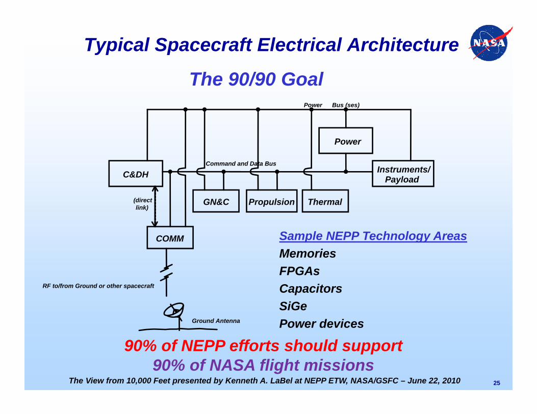
Typical Spacecraft Electrical Architecture
24The View from 10,000 Feet presented by Kenneth A. LaBel at NEPP ETW, NASA/GSFC – June 22, 2010
C&DH
Power
Instruments/Payload
GN&C Propulsion Thermal
COMM
Power Bus (ses)
Command and Data Bus
(directlink)
RF to/from Ground or other spacecraft
Ground Antenna
Sample NEPP Technology AreasMemoriesFPGAsCapacitorsSiGePower devices
90% of NEPP efforts should support90% of NASA flight missions
The 90/90 Goal
Typical Spacecraft Electrical Architecture
25The View from 10,000 Feet presented by Kenneth A. LaBel at NEPP ETW, NASA/GSFC – June 22, 2010

C&DH
Power
Instruments/Payload
GN&C Propulsion Thermal
COMM
Power Bus (ses)
Command and Data Bus
(directlink)
RF to/from Ground or other spacecraft
Ground Antenna
Sample NEPP Technology Areas
MemoriesUsed in any processing
application and for data storage on a spacecraft.
The 90/90 Goal - ExampleTypical Spacecraft Electrical Architecture
26The View from 10,000 Feet presented by Kenneth A. LaBel at NEPP ETW, NASA/GSFC – June 22, 2010

27
NEPP Has a Wide Range of Efforts• Tasks vary extensively in the technologies of
interest– Building blocks like capacitors– Standard products like DC-DC Converters, linear bipolar
devices, and A-to-D Converters– New commercial devices such as FPGAs and memories– Test structures on emerging commercial or radiation
hardened technologies– Specialized electronics such as IR arrays and fiber
optics– New assurance methods and investigations
• NEPP ETW provides forum to present recent results, as well as current and future plans
• Currently in FY11 planning cycle– PRELIMINARY PLANS FOLLOW
The View from 10,000 Feet presented by Kenneth A. LaBel at NEPP ETW, NASA/GSFC – June 22, 2010

NASA Electronic Parts Assurance Group (NEPAG)
Audits
NEPAG Focus Areas
Specs and Standards
US MIL
VCS
US MIL
DoD and NASA FundedNASA-only funded
Legend
Overguide
Core Areas are Bubbles;Boxes underneath are elements in each core
Failure Investigations
Investigate
Test/Analyze
Corrective Action
Lessons Learned
Assess NASA Impact
OffshoreOnshore
Collaborations
NationalInternational
NASA SAS Database
Parts Support
NPSL
Bulletins
Connectors
Technical Expertise Resource
Consortia
CAVECALCE
28The View from 10,000 Feet presented by Kenneth A. LaBel at NEPP ETW, NASA/GSFC – June 22, 2010

FY11 Radiation Plans for NEPP Core (1)
SiGe.Mixed Signal PhotonicsScaled
CMOSSensor
TechnologiesPerformance
Tools
Fiber Amplifiers
Exotic-dopedFiber components
Wavelength DivisionMultiplexing
Free spaceOptical interconnects
Fiber Data Links
NEPP Research Categories – Active Electronics
Ultra-low power
Silicon on Insulator (SOI)
IR
Visible
Cryo SEL
Test StructuresCommercial Devices
Memories –Non-volatile, volatile
FPGAs 32 and 45 nm
32 and 45 nm CMOS
SiGe
Low proton energy
Processors, SOCs CNTsStructured ASICS
Optocouplersand PM Optocouplers
SiGe on SOI
Scaled SiGeAdvanced
Data Conversion,Amplifiers, Drivers
Develops students atGeorgia Tech,
Vanderbilt, Auburn
Develops students
at Vanderbilt
RHBD Support
Partners include:DoD, IBM, TI, Intel, Boeing,
Actel, Atmel, Xilinx, Altera, Cypress
Partners at:AFRL, Cypress, Ball
DoD and NASA fundedNASA-only funded
Legend
Overguide
Architecturalcomparison
Others Compact model basedrate prediction
Core Areas are Bubbles;Boxes underneath are variable tasks in each core
29The View from 10,000 Feet presented by Kenneth A. LaBel at NEPP ETW, NASA/GSFC – June 22, 2010
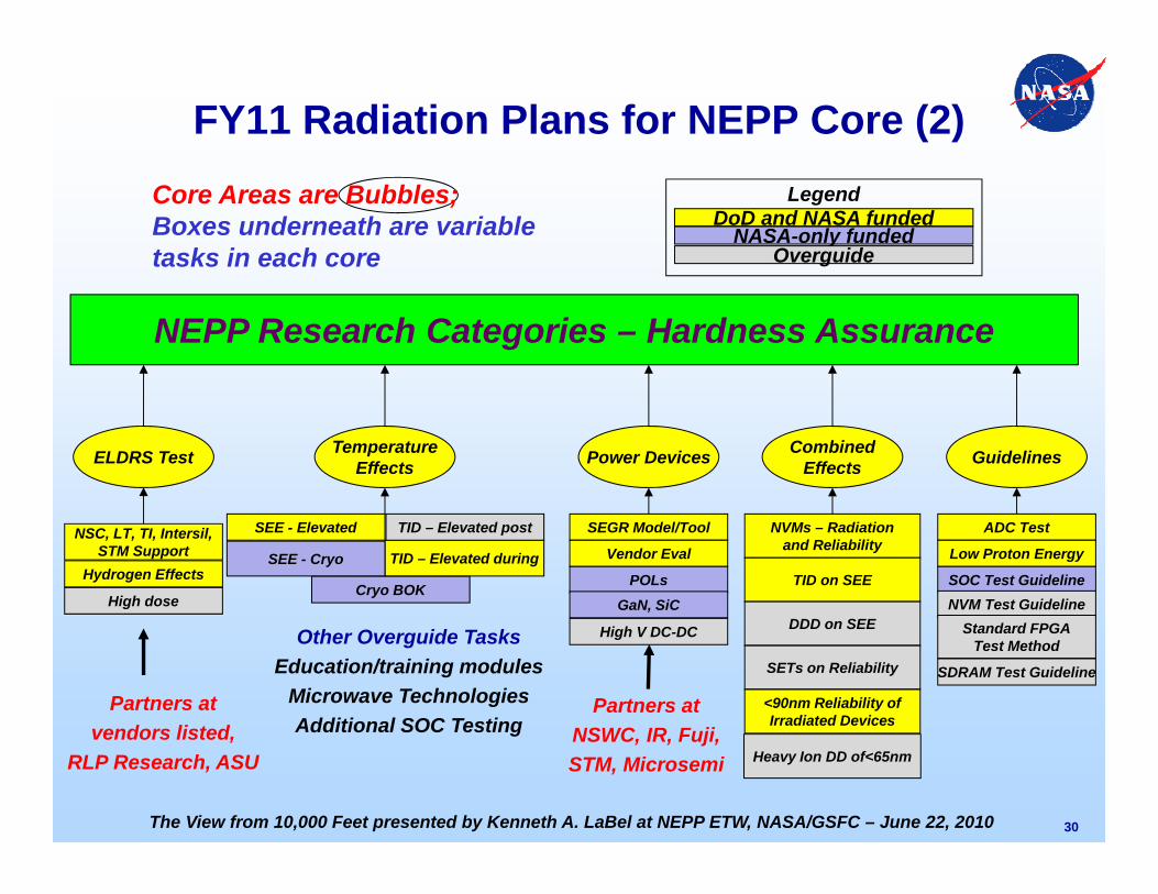
FY11 Radiation Plans for NEPP Core (2)
30
ELDRS Test CombinedEffects
TemperatureEffects Power Devices Guidelines
NVMs – Radiationand Reliability
TID on SEE
DDD on SEE
SETs on Reliability
<90nm Reliability ofIrradiated Devices
NEPP Research Categories – Hardness Assurance
TID – Elevated during
SEGR Model/Tool
Vendor Eval
POLs
TID – Elevated postSEE - Elevated
SEE - Cryo
Cryo BOK
ADC Test
Low Proton Energy
SOC Test Guideline
Heavy Ion DD of<65nm
NSC, LT, TI, Intersil,STM Support
Hydrogen Effects
GaN, SiC
Other Overguide TasksEducation/training modules
Microwave TechnologiesAdditional SOC Testing
NVM Test GuidelineStandard FPGA
Test Method
SDRAM Test Guideline
Partners atvendors listed,
RLP Research, ASU
Partners atNSWC, IR, Fuji,STM, Microsemi
High dose
High V DC-DC
DoD and NASA fundedNASA-only funded
Legend
Overguide
Core Areas are Bubbles;Boxes underneath are variable tasks in each core
The View from 10,000 Feet presented by Kenneth A. LaBel at NEPP ETW, NASA/GSFC – June 22, 2010

FY11 Parts Plans for NEPP Core (1)
SiGe.Mixed Signal PhotonicsScaled
CMOSSensor
Technologies Rf Electronics
Fiber Amplifiers
Exotic-dopedFiber components
Wavelength DivisionMultiplexing
Free spaceOptical interconnects
Fiber Data Links
NEPP Research Categories – Parts Assurance
Ultra-low power
Silicon on Insulator (SOI)
IR
Visible
ROICs - Cryo
Test StructuresCommercial Devices
Memories –Non-volatile
FPGAs 32 and 45 nm
RF Reliability Guide
Advanced RF
Processors, SOCs CNTsMemories - SDRAM
Optocouplersand PM Optocouplers
Cold temperatureeffects
Scaled SiGeAdvanced
Data Conversion,Amplifiers, Drivers
Sub 90nm
LegendNASA-only funded
Overguide
GaAs, InP, Antemonides
Others
Core Areas are Bubbles;Boxes underneath are variable tasks in each core
31The View from 10,000 Feet presented by Kenneth A. LaBel at NEPP ETW, NASA/GSFC – June 22, 2010
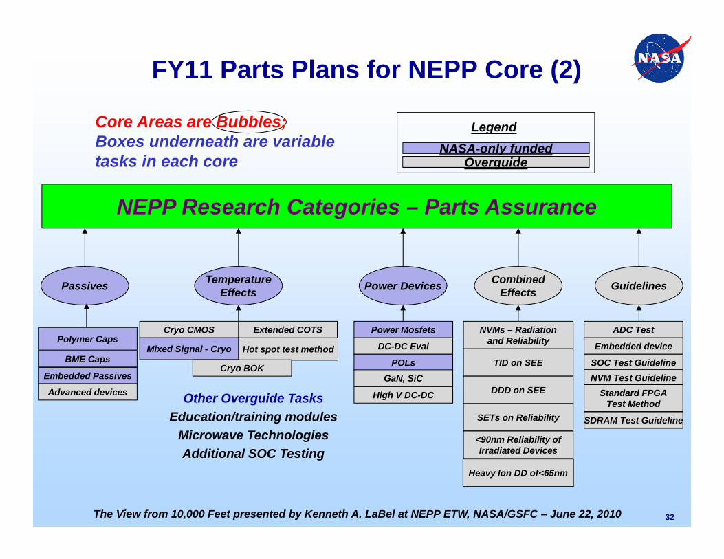
FY11 Parts Plans for NEPP Core (2)
Passives CombinedEffects
TemperatureEffects Power Devices Guidelines
NVMs – Radiationand Reliability
TID on SEE
DDD on SEE
SETs on Reliability
<90nm Reliability ofIrradiated Devices
NEPP Research Categories – Parts Assurance
Hot spot test method
Power Mosfets
DC-DC Eval
POLs
Extended COTSCryo CMOS
Mixed Signal - Cryo
Cryo BOK
ADC Test
Embedded device
SOC Test Guideline
Heavy Ion DD of<65nm
Polymer Caps
BME Caps
GaN, SiC
Other Overguide TasksEducation/training modules
Microwave TechnologiesAdditional SOC Testing
NVM Test GuidelineStandard FPGA
Test Method
SDRAM Test Guideline
Embedded Passives
High V DC-DCAdvanced devices
Core Areas are Bubbles;Boxes underneath are variable tasks in each core
LegendNASA-only funded
Overguide
32The View from 10,000 Feet presented by Kenneth A. LaBel at NEPP ETW, NASA/GSFC – June 22, 2010

Core Element - Packaging
–NEPP Research Categories – Advanced Packaging
NASA-only funded
Legend
Overvguide
Core Areas are Bubbles;Boxes underneath are variable tasks in each core
Area Arrays
Column Grid Arrays
Land Grid Arrays
Ball Grid Arrays
Lead-free
AssembliesTin Whiskers
Complex Non-
Hermetic
Area ArrayMIL Class Y
Materials
Embedded Technologies
ActivesPassives
Board Installation
Damage
Cracking
Parametric Drift
Reverse PolarityMicrocoil
Spring Array
33The View from 10,000 Feet presented by Kenneth A. LaBel at NEPP ETW, NASA/GSFC – June 22, 2010

34
Samples of NEPP Impact to the Community (1 of 2)
– MAP• Single Event Transients (SETs) –
anomaly resolution led to NASA alert
– TERRA• Optocouplers, Solid State
Recorders (SSR), High Gain Antenna anomaly
– AURA• Oscillators
– AQUA• Interpoint DC-DC converters
– TRMM, XTE• SSRs, FODBs
– TOPEX/Poseidon• Optocouplers
– SeaStar• SSRs
– Launch Vehicles• Optocouplers
– Suborbital• Parts screening
– Hubble Space Telescope• Optocouplers, Capacitors, SSRs,
Fiber Optic Data Bus (FODB)– Hubble Robotic Servicing
• Processors– JWST
• Detector technologies– Cassini
• Interpoint DC-DC converters, optocouplers, processors
– AXAF/Chandra• Optics
– SWIFT• ACTEL FPGAs
– MER• ELDRS, Processors, Memories,
Packaging– ISS
• Fiber optics, wire/cable– Shuttle
• ACTEL FPGAs, capacitors
NASA Flight Projects and some of the related areas that NEPP has provided a knowledge-base that has allowed anomaly/problem resolution
The View from 10,000 Feet presented by Kenneth A. LaBel at NEPP ETW, NASA/GSFC – June 22, 2010

35
Samples of NEPP Impact to the Community (2 of 2)
– Government partners• DoD
– USD(AT&L)– Defense Threat Reduction Agency
(DTRA)– Air Force Research Laboratory
(AFRL)– Air Force Space and Missile
Command (AFSMC)– Missile Defense Agency (MDA)– Defense Advanced Research
Projects Agency (DARPA)– NAVSEA– NAVAIR– Naval Research Laboratory– US Army Strategic and Missile
Defense Command (USASMDC)– OGA
• DOE– Sandia National Laboratories– Lawrence Livermore National
Laboratories– Brookhaven National Laboratories
• NSF– National Superconducting Cyclotron
Laboratory• ESA• JAXA• CNES• Qinetiq (UK)
– Industry partners• Actel• Lambda/International Rectifier• Interpoint• Vishay• Presidio• BAE Systems• Honeywell• Aeroflex• Intersil• Xilinx• IBM• Freescale (formerly Motorola)• Cardinal• LSI Logic• Ball Aerospace• Micro RDC, many others
NEPP has supported DoD and other government anomaly/problem issues, technology developments, as well as joint knowledge-base development that have import to the NASA
communityIn addition, NEPP has worked with industry to develop improved products for spaceflight
The View from 10,000 Feet presented by Kenneth A. LaBel at NEPP ETW, NASA/GSFC – June 22, 2010

QUESTIONS?
36The View from 10,000 Feet presented by Kenneth A. LaBel at NEPP ETW, NASA/GSFC – June 22, 2010