clock talk live schedule presentation will begin shortly
TRANSCRIPT

Clock Talk LIVE Schedule – Presentation will begin shortly
Tuesday, Sept 15th IEEE 1588 Timing Solutions for Non-Telecom Applications
Tuesday, Sept 29th Clock Jitter Demystified and Jitter Requirements for 56/112 SerDes
Tuesday, Oct 13thDesign Considerations When Selecting a XO/VCXO Clock Reference for 56G/112G SerDes
Tuesday, Oct 27thStop Guessing, Use Silicon Labs’ Timing Tools to Build Your Clock Tree
Tuesday, Nov 10thOptimize Timing Solutions for High Speed FPGA and Application Processor Designs
Tuesday, Nov 17th PCIe Gen 4/5/6 Specifications and Jitter Measurement Explained
Tuesday, Dec 1st Timing Solutions for 5G O-RAN Systems
Tuesday, Jan 12th AEC-Q100 Timing Products for Automotive Applications
Tuesday, Jan 26th Timing Solutions for Open-Compute Systems
1
Register for the series at: https://www.silabs.com/clock-talk
WELCOME SILICON LABS LIVE
Internet Infrastructure andIndustrial Automation Tech Talks
2
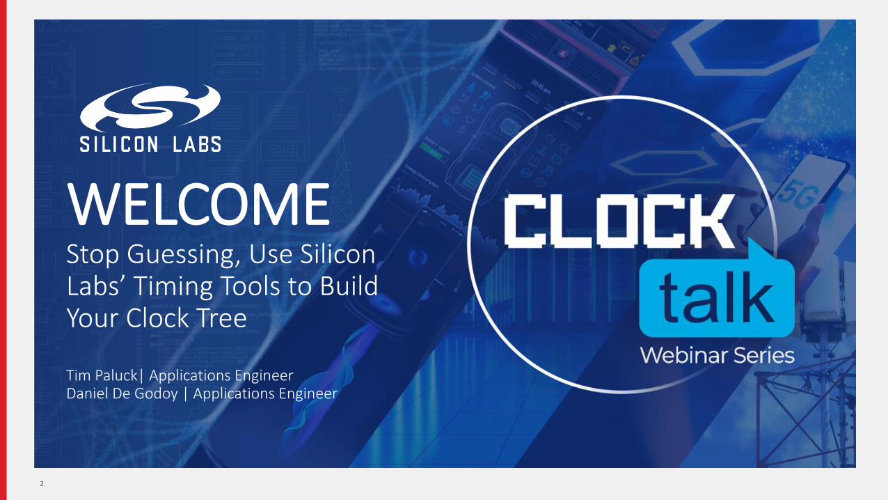
WELCOMEStop Guessing, Use Silicon Labs’ Timing Tools to Build Your Clock Tree
Tim Paluck| Applications EngineerDaniel De Godoy | Applications Engineer
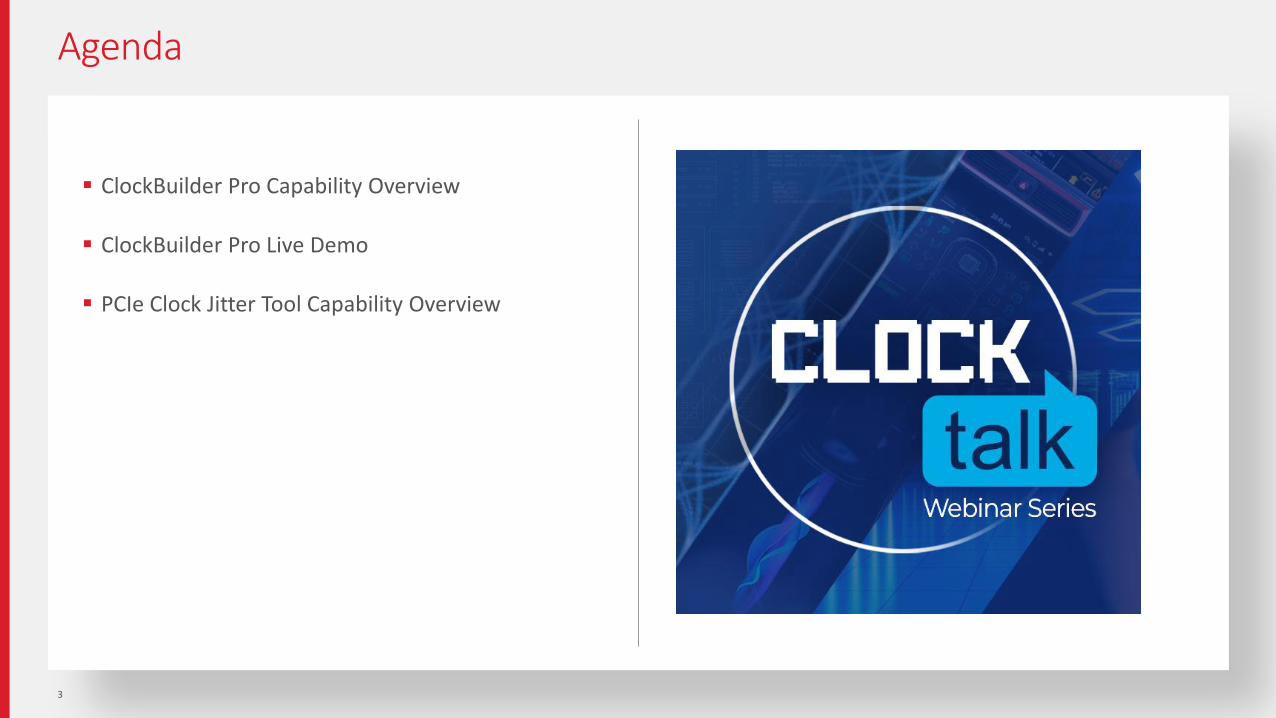
▪ ClockBuilder Pro Capability Overview
▪ ClockBuilder Pro Live Demo
▪ PCIe Clock Jitter Tool Capability Overview
Agenda
3
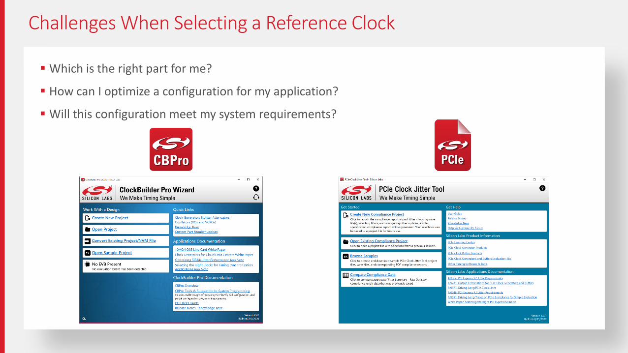
▪ Which is the right part for me?
▪ How can I optimize a configuration for my application?
▪ Will this configuration meet my system requirements?
Challenges When Selecting a Reference Clock
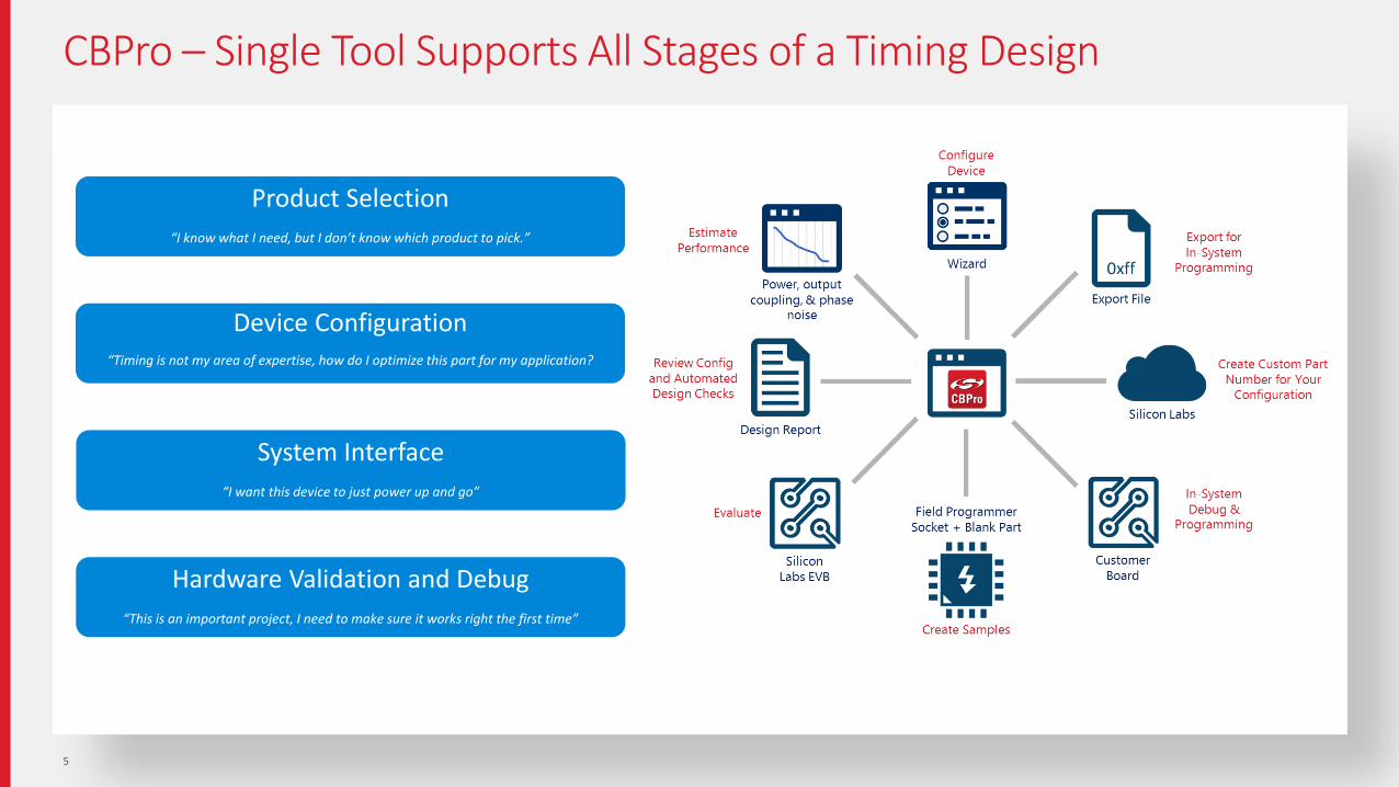
CBPro – Single Tool Supports All Stages of a Timing Design
5
Product Selection
“I know what I need, but I don’t know which product to pick.”
Device Configuration“Timing is not my area of expertise, how do I optimize this part for my application?
Hardware Validation and Debug
“This is an important project, I need to make sure it works right the first time”
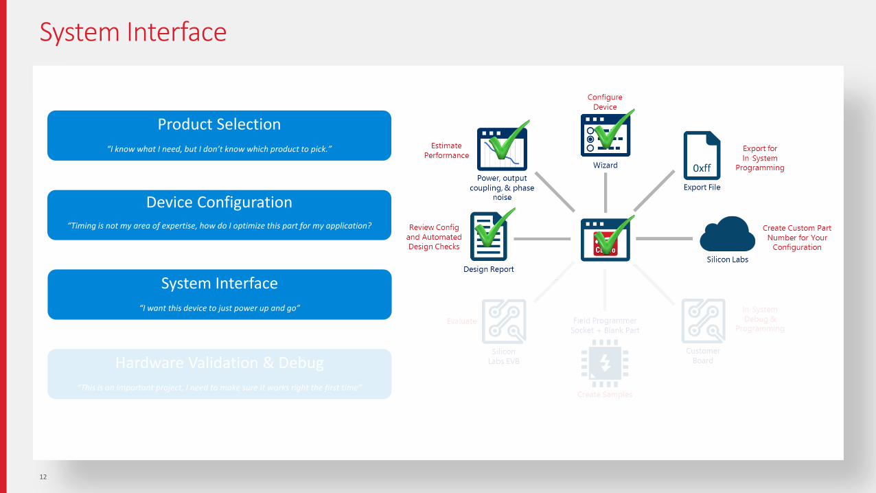
System Interface
“I want this device to just power up and go”
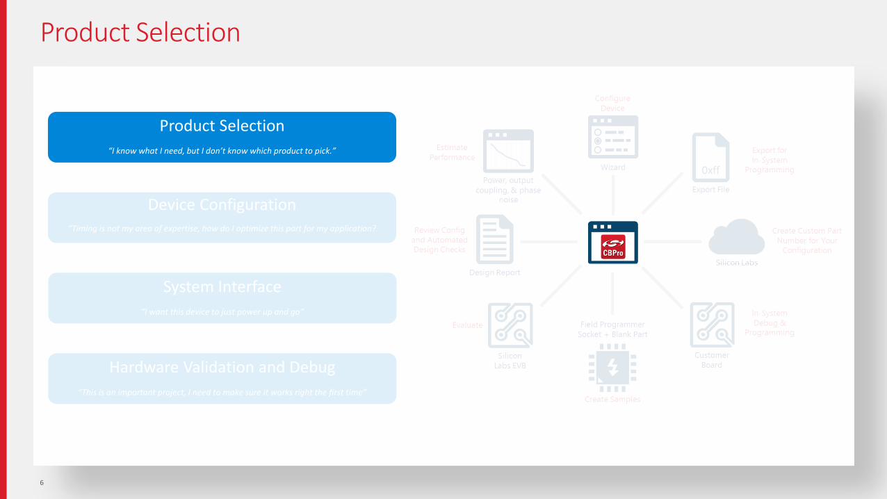
Product Selection
6
Product Selection
“I know what I need, but I don’t know which product to pick.”
Device Configuration“Timing is not my area of expertise, how do I optimize this part for my application?
Hardware Validation and Debug
“This is an important project, I need to make sure it works right the first time”
System Interface
“I want this device to just power up and go”
Product Selection
7
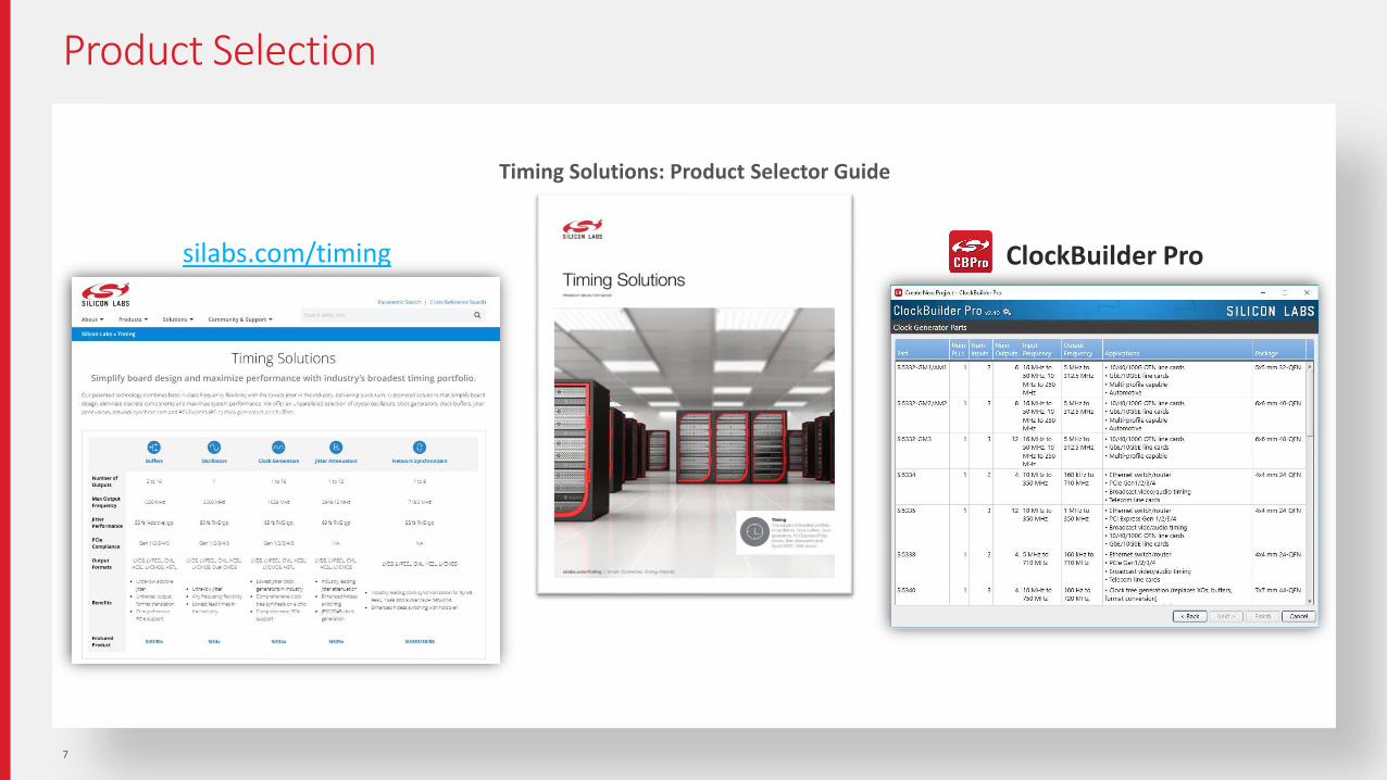
silabs.com/timing
Timing Solutions: Product Selector Guide
ClockBuilder Pro
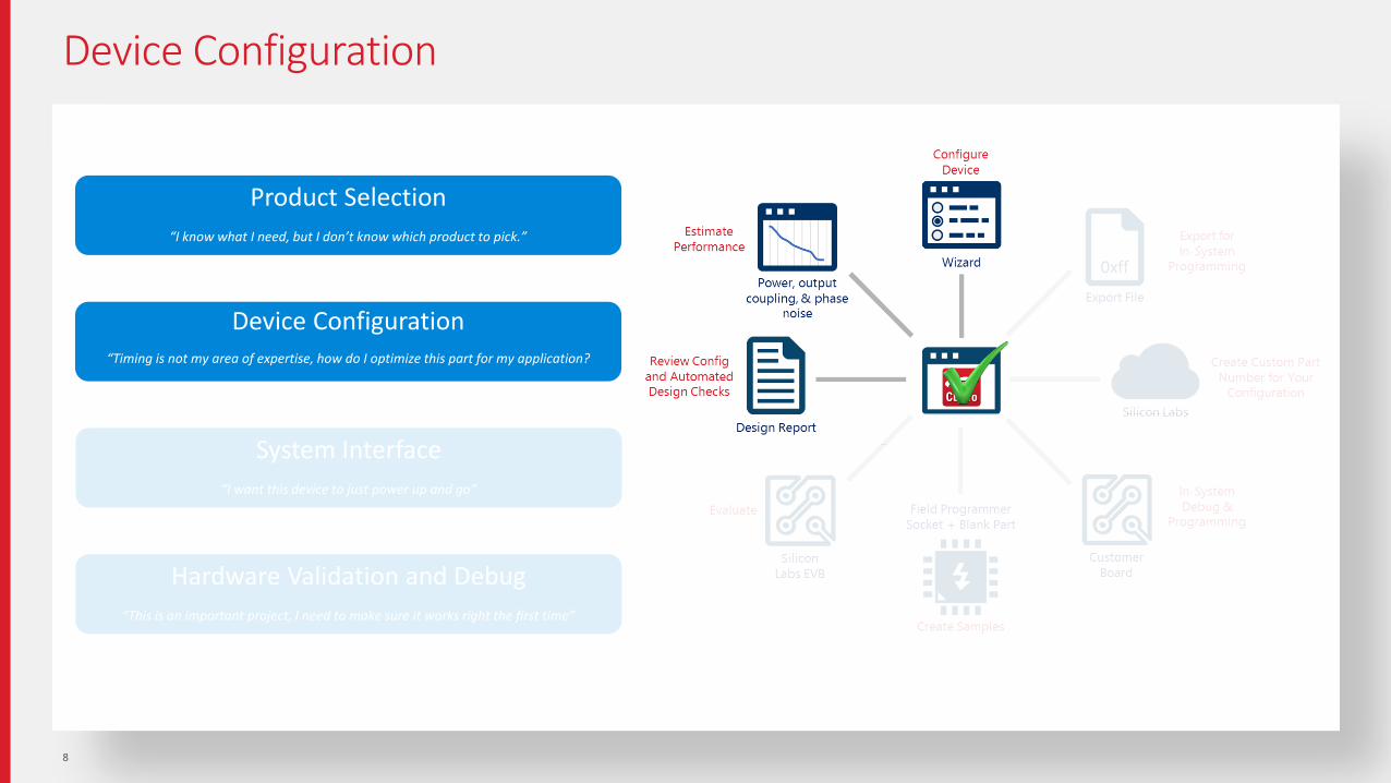
Device Configuration
8
Product Selection
“I know what I need, but I don’t know which product to pick.”
Device Configuration“Timing is not my area of expertise, how do I optimize this part for my application?
Hardware Validation and Debug
“This is an important project, I need to make sure it works right the first time”
System Interface
“I want this device to just power up and go”
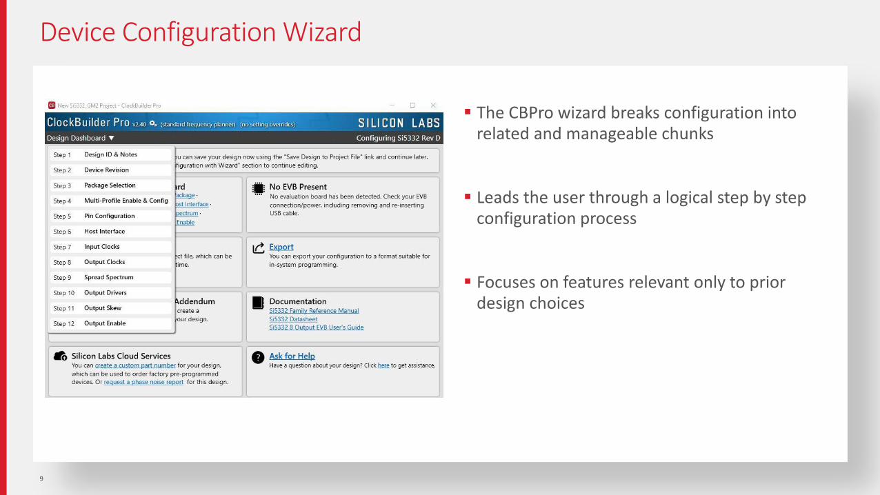
Device Configuration Wizard
9
▪ The CBPro wizard breaks configuration into related and manageable chunks
▪ Leads the user through a logical step by step configuration process
▪ Focuses on features relevant only to prior design choices
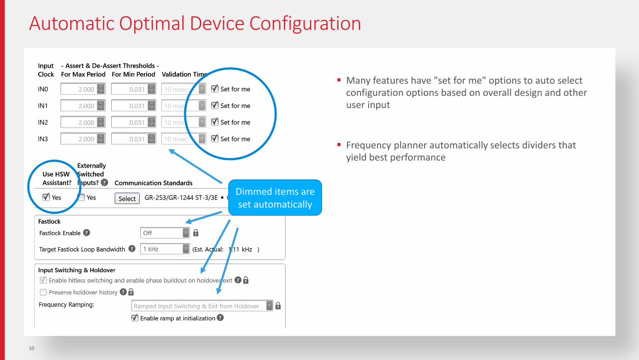
Automatic Optimal Device Configuration
▪ Many features have "set for me" options to auto select configuration options based on overall design and other user input
▪ Frequency planner automatically selects dividers that yield best performance
10
Dimmed items are set automatically

Design Rule Checks (DRCs)
▪ CBPro checks your configuration for errors and potential issues (warnings) in real-time
▪ Always visible DRC widget provides centralized clearing house for errors and warnings, making it easy to track whether your design is issue free
▪ Also included in design report
▪ You must review and approve if custom part number is created
11
System Interface
12
Product Selection
“I know what I need, but I don’t know which product to pick.”
Device Configuration“Timing is not my area of expertise, how do I optimize this part for my application?
Hardware Validation & Debug
“This is an important project, I need to make sure it works right the first time”
System Interface
“I want this device to just power up and go”
Export or OPN?
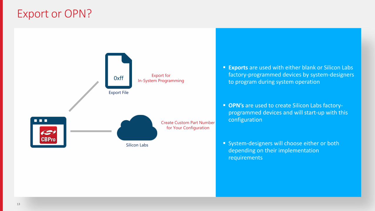
▪ Exports are used with either blank or Silicon Labs factory-programmed devices by system-designers to program during system operation
▪ OPN’s are used to create Silicon Labs factory-programmed devices and will start-up with this configuration
▪ System-designers will choose either or both depending on their implementation requirements
13
Silicon Labs
0xff
Export File
Create Custom Part Number
for Your Configuration
Export for
In-System Programming
Export or OPN?
14
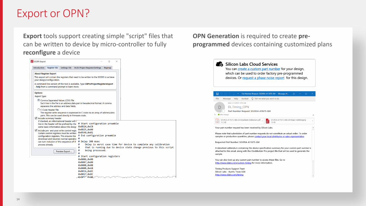
Export tools support creating simple "script" files that can be written to device by micro-controller to fully reconfigure a device
OPN Generation is required to create pre-programmed devices containing customized plans
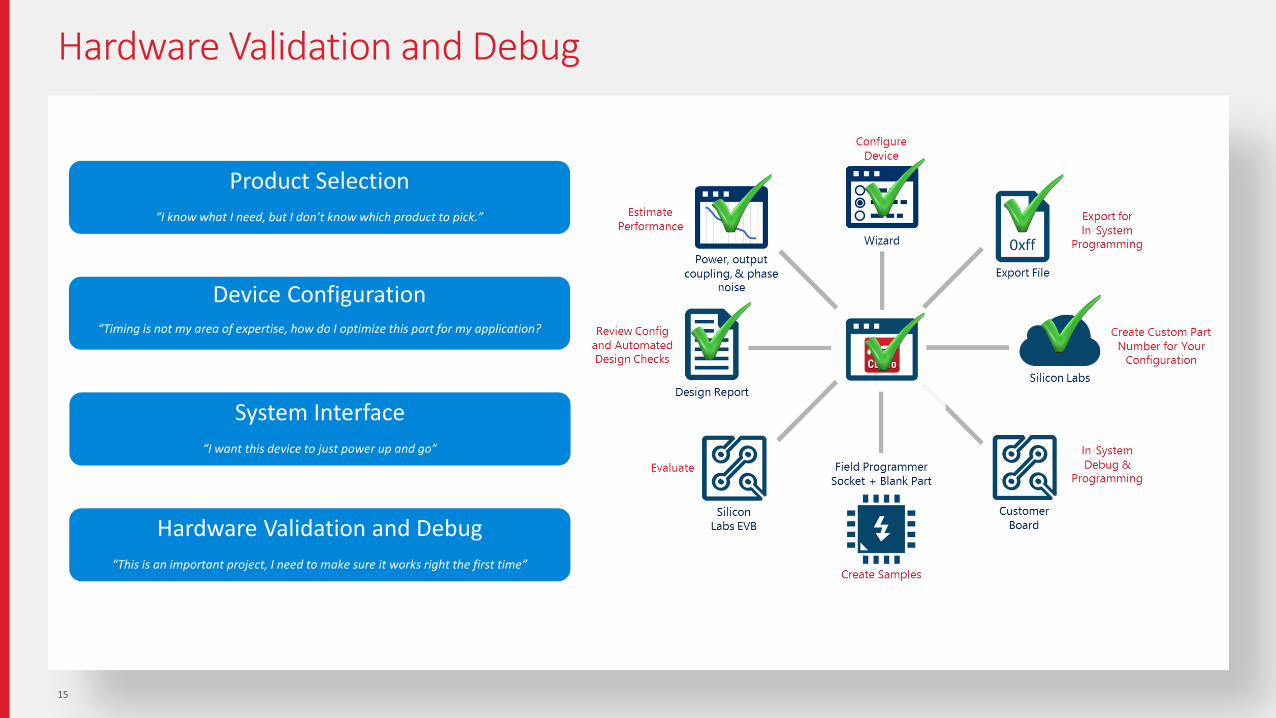
Hardware Validation and Debug
15
Product Selection
“I know what I need, but I don’t know which product to pick.”
Device Configuration“Timing is not my area of expertise, how do I optimize this part for my application?
Hardware Validation and Debug
“This is an important project, I need to make sure it works right the first time”
System Interface
“I want this device to just power up and go”
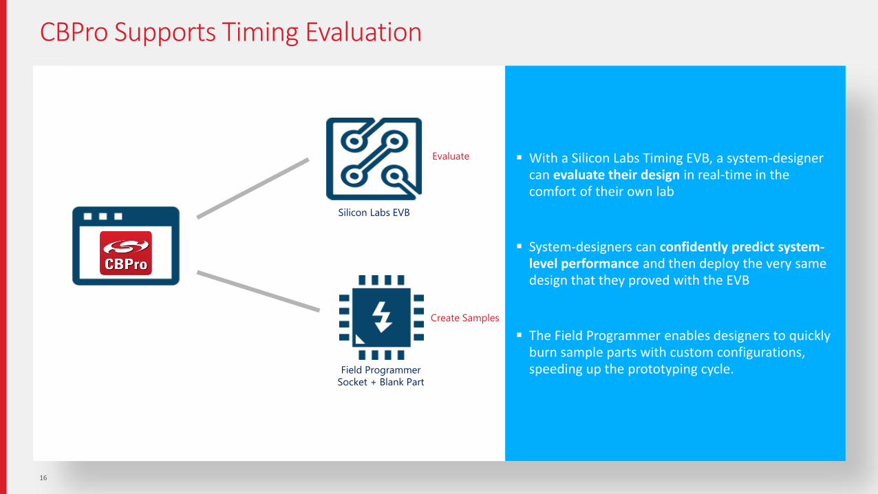
CBPro Supports Timing Evaluation
▪ With a Silicon Labs Timing EVB, a system-designer can evaluate their design in real-time in the comfort of their own lab
▪ System-designers can confidently predict system-level performance and then deploy the very same design that they proved with the EVB
▪ The Field Programmer enables designers to quickly burn sample parts with custom configurations, speeding up the prototyping cycle.
16
Evaluate
Silicon Labs EVB
Field Programmer
Socket + Blank Part
Create Samples
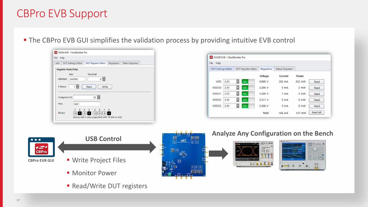
CBPro EVB Support
17
CBPro EVB GUI
USB Control
▪ The CBPro EVB GUI simplifies the validation process by providing intuitive EVB control
▪ Write Project Files
▪ Monitor Power
▪ Read/Write DUT registers
Analyze Any Configuration on the Bench

The CBPro Field Programmer (CBPROG-DONGLE)
▪ The Field Programmer enables CBPro functionality anywhere!
▪ Read/write settings and registers
▪ Burn the NVM of blank devices
▪ Write a CBPro project file
▪ Flash firmware and configuration
▪ Communicate with in-system soldered down devices using a standard 10-pin header and a ribbon cable
▪ Pair it with a socket adapter to program the NVM of loose samples
▪ See UG286 for a detailed User’s Guide
18

CBPro – Single Tool Supports All Stages of a Timing Design
19
Product Selection
“I know what I need, but I don’t know which product to pick.”
Device Configuration“Timing is not my area of expertise, how do I optimize this part for my application?
Hardware Validation and Debug
“This is an important project, I need to make sure it works right the first time”
System Interface
“I want this device to just power up and go”
Clock Builder Pro Live Demo

The most
complete
and easy to use
PCIe Reference Clock Compliance Tool
Silicon Labs PCIe Clock Jitter Tool
21
Download it free at:https://www.silabs.com/timing/pci-express-learning-center
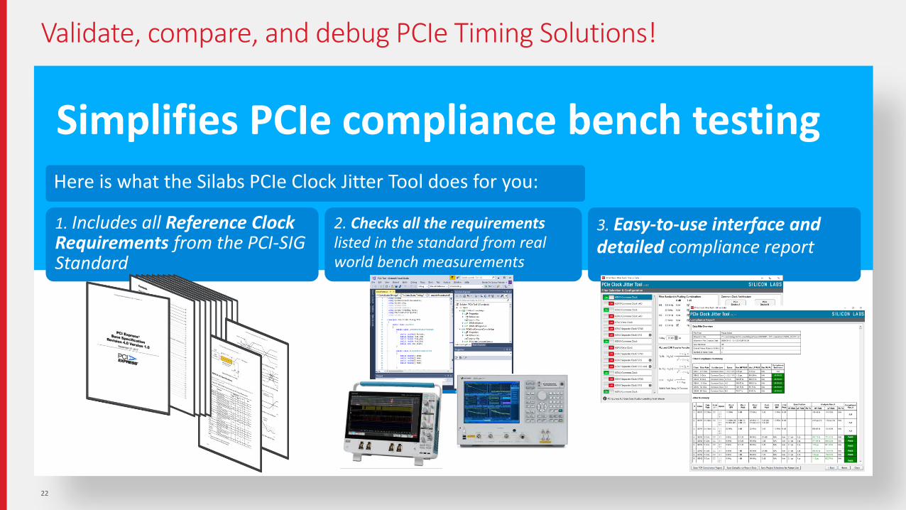
1. Includes all Reference ClockRequirements from the PCI-SIG Standard
2. Checks all the requirementslisted in the standard from real world bench measurements
3. Easy-to-use interface and detailed compliance report
Validate, compare, and debug PCIe Timing Solutions!
22
Simplifies PCIe compliance bench testingHere is what the Silabs PCIe Clock Jitter Tool does for you:
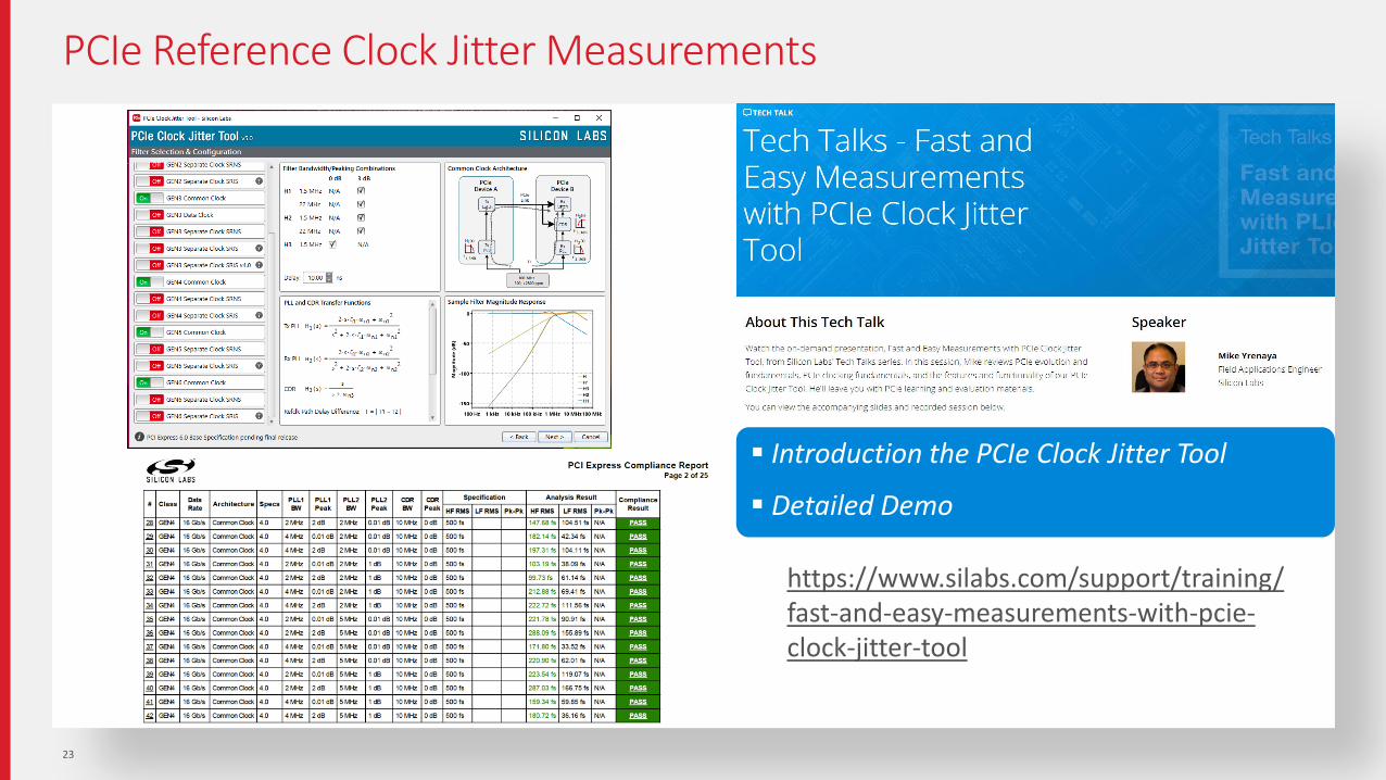
PCIe Reference Clock Jitter Measurements
23
https://www.silabs.com/support/training/fast-and-easy-measurements-with-pcie-clock-jitter-tool
▪ Introduction the PCIe Clock Jitter Tool
▪ Detailed Demo
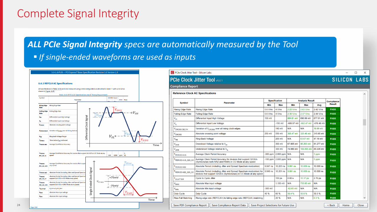
Complete Signal Integrity
24
ALL PCIe Signal Integrity specs are automatically measured by the Tool
▪ If single-ended waveforms are used as inputs
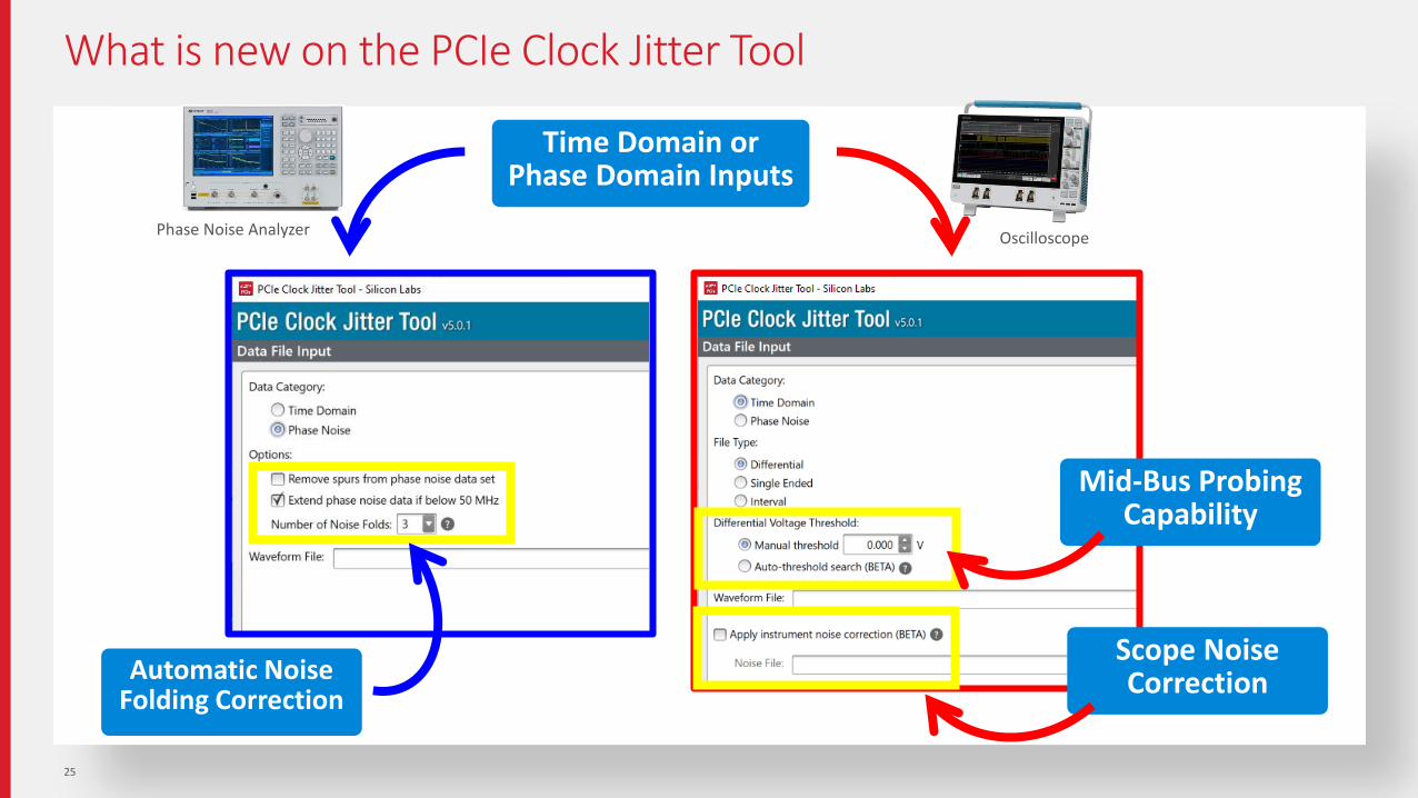
What is new on the PCIe Clock Jitter Tool
25
Time Domain or Phase Domain Inputs
Automatic Noise Folding Correction
Mid-Bus Probing Capability
Scope Noise Correction
Phase Noise Analyzer Oscilloscope

Time Domain or Phase Domain Jitter Measurement
26
“Jitter measurements may be used with a Phase Noise Analyzer (PNA) extending (flat) and integrating and folding the frequency content up to an offset from the carrier frequency of at least 200 MHz (at 300 MHz absolute frequency) below the Nyquist frequency.”
PCI-SIG GEN5 Table 8-18, note 2
Phase Noise Analyzer
Oscilloscope
The Silabs Clock Jitter accepts both• Time-Domain capture from your oscilloscope• Phase-Domain measurement from your PNA
Both are valid, but they are fundamentally different measurements:
• Phase-Domain → Analog Jitter Measurement• Time-Domain → Sampled Jitter Measurement
For Phase-Domain jitter measurements, the PCI-SIG requires a noise folding correction
• Emulates high-frequency content being folded back to in band
Phase Noise with Folding Correction
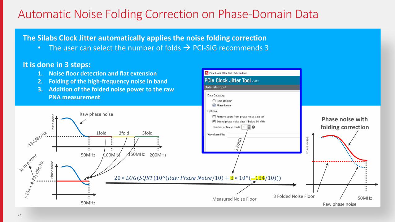
Automatic Noise Folding Correction on Phase-Domain Data
27
50MHz 100MHz 150MHz 200MHz
1fold 2fold 3fold
50MHz
Ph
ase
no
ise
Ph
ase
no
ise
20 ∗ 𝐿𝑂𝐺(𝑆𝑄𝑅𝑇(10^(𝑅𝑎𝑤 𝑃ℎ𝑎𝑠𝑒 𝑁𝑜𝑖𝑠𝑒/10) + 3 ∗ 10^(−134/10)))
Measured Noise Floor 50MHz
Ph
ase
no
ise
3 Folded Noise Floor
Raw phase noise
Phase noise with folding correction
The Silabs Clock Jitter automatically applies the noise folding correction• The user can select the number of folds → PCI-SIG recommends 3
It is done in 3 steps:1. Noise floor detection and flat extension 2. Folding of the high-frequency noise in band 3. Addition of the folded noise power to the raw
PNA measurement
Raw phase noise

Mid-Bus Probing Capability
28
PCB
Ref Clock Ref Clock Receiver
Closest probing point to the load at Mid-Bus
Mid-Bus Probing Load Probing
Automatically sets the threshold that allows jitter measurements even with
significant reflections
Clock Trace
Via
The Silabs Clock Jitter can adjust the threshold when it is not possible to probe at load• Probing a mid-bus can distort the signal, causing multiple 0V crossing whiting a single period
To avoid erroneous period calculations the tool:• Allows the user to manually shift the threshold used to detect edges• Has an internal algorithm that looks for the optimal threshold location to optimize jitter
measurement
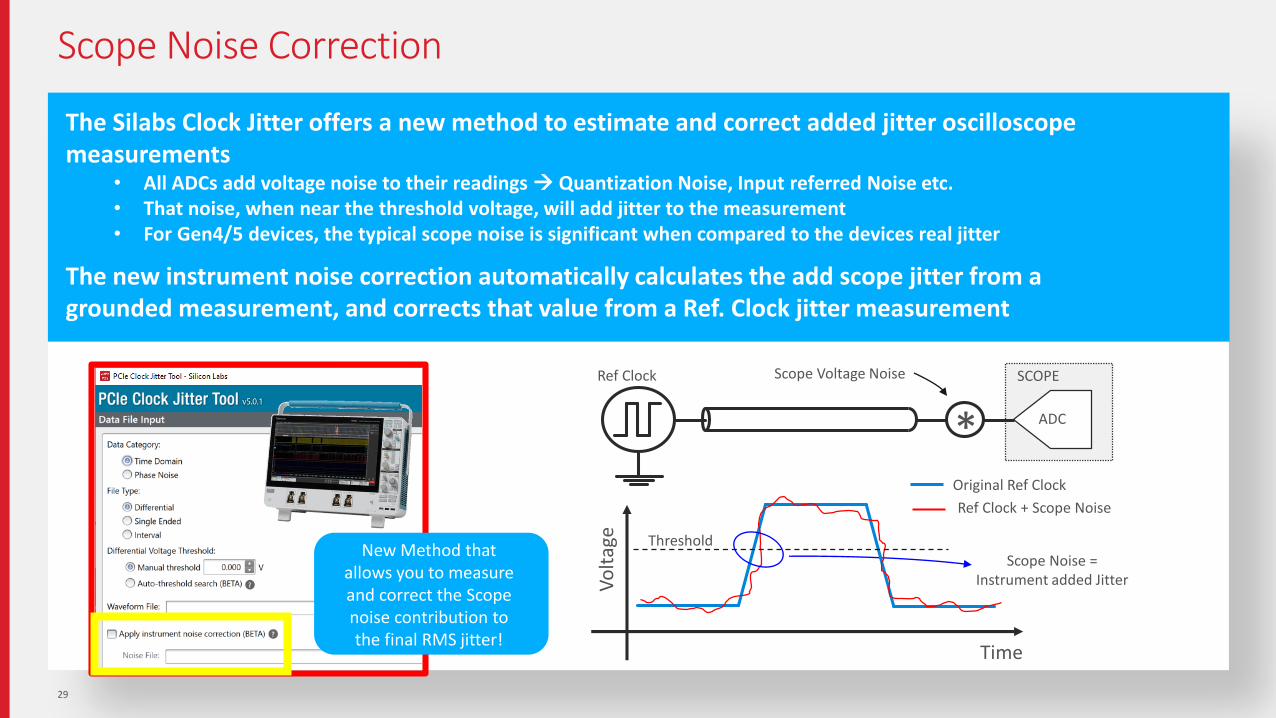
Scope Noise Correction
29
ADC
SCOPE
*
Ref Clock Scope Voltage Noise
Vo
ltag
e
Time
Original Ref Clock
Ref Clock + Scope Noise
Threshold
Scope Noise = Instrument added Jitter
New Method that allows you to measure and correct the Scope noise contribution to the final RMS jitter!
The Silabs Clock Jitter offers a new method to estimate and correct added jitter oscilloscope measurements
• All ADCs add voltage noise to their readings → Quantization Noise, Input referred Noise etc.• That noise, when near the threshold voltage, will add jitter to the measurement• For Gen4/5 devices, the typical scope noise is significant when compared to the devices real jitter
The new instrument noise correction automatically calculates the add scope jitter from a grounded measurement, and corrects that value from a Ref. Clock jitter measurement

Scope Noise Removal: Experimental Data
30
The Silabs Clock Jitter offers a new method to estimate and correct added jitter oscilloscope measurements
• All ADCs add voltage noise to their readings → Quantization Noise, Input referred Noise etc.• That noise, when near the threshold voltage, will add jitter to the measurement• For Gen4/5 devices, the typical scope noise is significant when compared to the devices real jitter (~40%)
0.000
0.050
0.100
0.150
0.200
0.250
0.300
0.350
0.400
0.450
0 1 2 3 4 5 6
PC
Ie G
en5
Max
RM
S H
F (p
s)
Device
MSO 50 SSOFF
MSO 50 SSOFF SNR
MSO PRB SSOFF
MSO PRB SSOFF SNR
PN 0 FOLD
PN 3 FOLD
DSA 50 SSOFF
DSA 50 SSOFF SNR
PCIe Gen5 Limit
Silabs PCIe Clock Jitter Tool Scope Noise Removal
Si52200 Si5332 EX NO Si5332 EX O0 Si5332 IX NO Si5332 IX O0
Summary
31
1. Complete Signal Integrity Measurements
2. Jitter Measurements
a) Time Domain versus Phase Domain Jitter Measurement
b) Noise Folding
c) Mid-Bus Probing
d) Scope Noise Removal
Clock Talk:PCIe Gen 4/5/6 Specifications and Jitter Measurement Explained
TUES, NOV 17TH AT 9:00 CST/16:00 CETWEDS, NOV 18TH AT 10:30 HKT

▪ Download ClockBuilder Pro HERE
▪ CBPro Tools & Support for In-System Programming
▪ Command Line Interface (CLI) User’s Guide
▪ ClockBuilder Pro Field Programmer (CBPROG-DONGLE) product page
▪ Download the PCIe Clock Jitter tool HERE
▪ Watch the PCIe Clock Jitter Tech Talk HERE
Additional Resources
32
WELCOME SILICON LABS LIVE
Internet Infrastructure andIndustrial Automation Tech Talks
33
Thank you!

WELCOME SILICON LABS LIVE
Internet Infrastructure andIndustrial Automation Tech Talks
34
Q&A