clock signal in electronic systems
TRANSCRIPT
1
Nanometer Frequency Synthesis Beyond the Phase-Locked Loop, First Edition. Liming Xiu.© 2012 The Institute of Electrical and Electronics Engineers, Inc. Published 2012 by John Wiley & Sons, Inc.
CHAPTER 1
CLOCK SIGNAL IN ELECTRONIC SYSTEMS
1.1 THE SIGNIFICANCE OF CLOCK SIGNAL
1.1.1 Clock Signal
In modern electronic - driven society, our everyday lives are supported by various kinds of electronic devices. At home, TV, computer, audio system, game machine, and digital camera are indispensable for our entertainment and relaxation. Away from home, mobile phones keep us connected with the world all the time. On the road, automobiles and airplanes with countless built - in electronic devices make them safe to be driven/fl own and comfortable to ride in. At work, we spend most of our time dealing with the computer, fax machine, copier, printer, projector, etc. Without these electronic devices, people ’ s lives would be totally different; human society would regress many years in stan-dard of living. Electronic devices have already penetrated into all aspects of our lives.
When in operation, almost all electronic devices rely on a very important signal: the clock. This is simply due to the fact that electronic devices are made of very - large - scale - integration (VLSI) chips, which are primarily designed on the synchronous principle. For any chip, simple or complex, its designed func-tionality is achieved by millions of events that occur inside it. These events do not happen randomly but in a predetermined, orderly sequence. The clock signal is the conductor of the orchestra to produce harmony. For successful
COPYRIG
HTED M
ATERIAL
2 CLOCK SIGNAL IN ELECTRONIC SYSTEMS
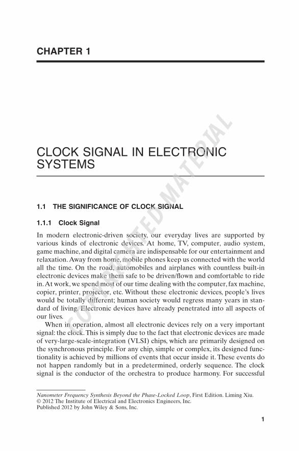
operation in a large chip, many clock signals (as many as hundreds) could be required simultaneously. Usually, phase - locked loop ( PLL ) is used on - chip to generate these crucial clock signals. If a VLSI chip could be treated as a person and the on - chip processor were regarded as the brain, then the clock pulse is the heartbeat, the clock signal is the blood, and the clock distribution network (clock tree) is the vessel. This analogy is graphically demonstrated in Fig. 1.1 .
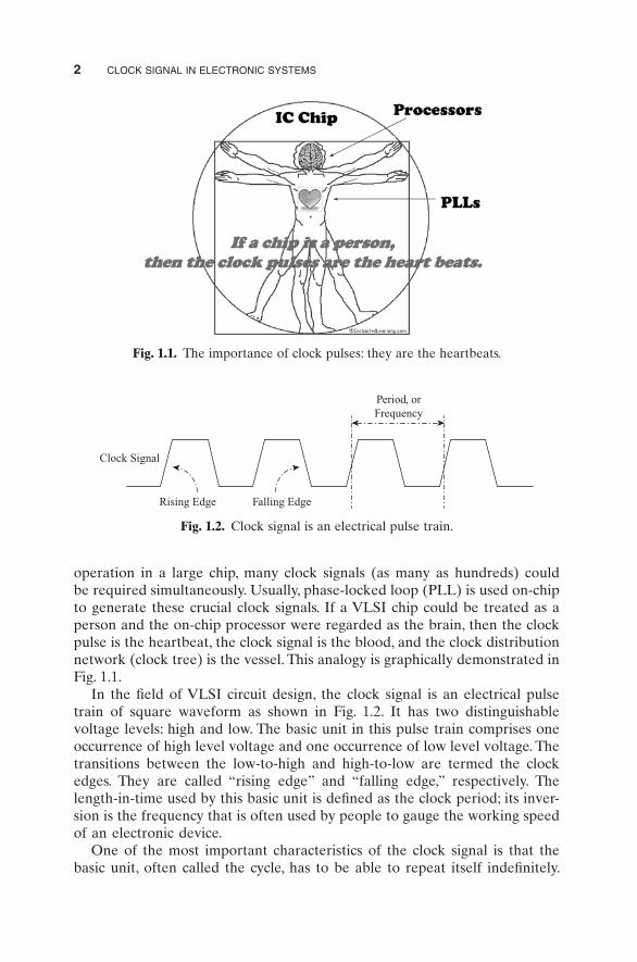
In the fi eld of VLSI circuit design, the clock signal is an electrical pulse train of square waveform as shown in Fig. 1.2 . It has two distinguishable voltage levels: high and low. The basic unit in this pulse train comprises one occurrence of high level voltage and one occurrence of low level voltage. The transitions between the low - to - high and high - to - low are termed the clock edges. They are called “ rising edge ” and “ falling edge, ” respectively. The length - in - time used by this basic unit is defi ned as the clock period; its inver-sion is the frequency that is often used by people to gauge the working speed of an electronic device.
One of the most important characteristics of the clock signal is that the basic unit, often called the cycle, has to be able to repeat itself indefi nitely.
Fig. 1.1. The importance of clock pulses: they are the heartbeats.
Fig. 1.2. Clock signal is an electrical pulse train.
Clock Signal
Rising Edge Falling Edge
Period, orFrequency

THE SIGNIFICANCE OF CLOCK SIGNAL 3
In other words, in this pulse train, every cycle has to be exactly the same. This is because that clock signal is the driver of the chip. The billions of operations (can also be viewed as events) inside a VLSI chip are all coordi-nated by clock signal. Structurally, the circuit inside the chip is designed in such way that these operations are triggered by either the rising edge or the falling edge, or both, of the clock signal. Therefore, it is essential that the occurrences of these edges in time are precisely predictable. The easiest way of achieving this goal is to make every cycle the same. A clock signal with this predictability in its waveform has enabled an important VLSI circuit design method: synchronous design. The synchronous design methodology is a milestone technology that allows the VLSI chip design industry to make great strides.
The physical medium inside the electronic circuit is electrical voltage or current. The electronic circuit is naturally suitable for handling the magnitude of this medium. (In all VLSI chips, information is represented through the magnitude of this medium.) By manipulating the magnitude, VLSI chips can process information and produce result for us to use. Manipulating the medi-um ’ s magnitude for representing information is natural for an electronic circuit, since magnitude is directly proportional to the number of electronics fl owing inside electronic devices. On the other hand, an electronic circuit is not naturally born for managing the other important variable: time . Instead, electronic systems use voltage transition to represent timing information. Therefore, it is not an easy task to generate the period of the basic unit (clock cycle) any way you want. It usually requires external help of a timing reference source, such as a mechanical crystal oscillator. Then, a special circuitry of PLL is used to produce other time scales based on this precise reference. This fi eld of work is called frequency synthesis, and it is one of the most actively researched and engineered areas in VLSI circuit design.
1.1.2 The Aim of This Book
Due to the diffi culty of using electronic circuits to manipulate the time scale, the capability of PLLs is limited. In many cases, it is extremely diffi cult and costly for the clock circuit design engineer to produce the clock frequencies that the system engineer prefers. Most of the time, the system engineer has to use whatever frequencies the PLL circuit designer is able to offer. Moreover, when a PLL is used as the clock source, it is diffi cult to switch from one fre-quency to another in a short time (a short time in comparison to the clock period). Consequently, these problems have limited our options for designing better and cheaper electronic products.
Throughout the history of frequency synthesis development, there are three distinguished approaches: direct analog synthesis, direct digital fre-quency synthesis ( DDFS ), and PLL - based indirect frequency synthesis. Among these, the PLL - based method is the most popular one for on - chip clock generation. There are several styles in the PLL - based approach:
4 CLOCK SIGNAL IN ELECTRONIC SYSTEMS
integer - N PLL, fractional - N PLL, sigma - delta fractional - N PLL, and all digital PLL ( ADPLL ). All the aforesaid techniques are built around one basic con-sensus: constructing the clock waveform with equal lengths in time for all the cycles. In other words, the basic unit of the clock waveform is repeatable; all the units have to be exactly the same. This feature is ideal for the clock that is being used as the driver signal for chip operation because the location in time of every edge is precisely predictable. Unfortunately, this is also the single most infl uencing factor that makes the task of clock generation (fre-quency synthesis) diffi cult.
History shows that major science and technology advancements often start with adventurous thinking. Breakthroughs usually happen when traditional thinking is detoured. Moreover, most of the time, crucial advancement is ini-tialized at the conceptual level. After a long period of time sticking with the belief that “ all cycles shall have same length - in - time, ” it is worth focusing our attention back to the two fundamental issues:
1. In the fi eld of electronic circuit design, what does frequency mean? 2. In circuit design practice, how is the clock signal used?
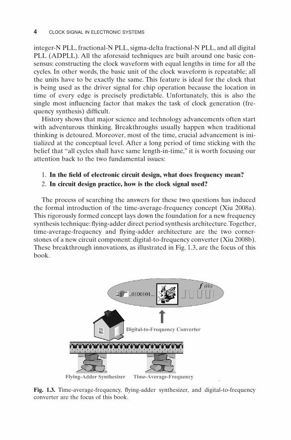
The process of searching the answers for these two questions has induced the formal introduction of the time - average - frequency concept (Xiu 2008a ). This rigorously formed concept lays down the foundation for a new frequency synthesis technique: fl ying - adder direct period synthesis architecture. Together, time - average - frequency and fl ying - adder architecture are the two corner-stones of a new circuit component: digital - to - frequency converter (Xiu 2008b ). These breakthrough innovations, as illustrated in Fig. 1.3 , are the focus of this book.
Fig. 1.3. Time - average - frequency, fl ying - adder synthesizer, and digital - to - frequency converter are the focus of this book.
THE CHARACTERISTICS OF CLOCK SIGNAL 5
1.2 THE CHARACTERISTICS OF CLOCK SIGNAL
The clock signal used in electronic system has two functional characteristics: frequency and phase. It also has one quality - related characteristic: jitter (phase noise). A clock period is defi ned as the time used by one clock cycle. The frequency, which is the mathematical inverse of the period, is used to describe the number of clock cycles (clock pulses) that exist in the time frame of 1 second. In modern synchronous design practice, all the events that happen inside a chip are triggered by either the rising edge or the falling edge, or both, of the clock pulses. Therefore, frequency determines the number of operations carried out within 1 second. It is the gauge of chip speed. For example, a CPU running at 2 GHz has 2 billion clock pulses within 1 second. Consequently, there will be 2 billion coordinated operations that occur within 1 second. Fre-quency is the most important characteristic of the clock signal. When more than two clock signals exist in a system and interact with each other (through the data they drive), in addition to their frequencies, the relative positions of their functional edges are of interest to system designer as well. This relative position is represented through a parameter called the clock phase. The preci-sion associated with the position of the clock ’ s functional edge is qualifi ed by another parameter of jitter.
1.2.1 Jitter and Phase Noise
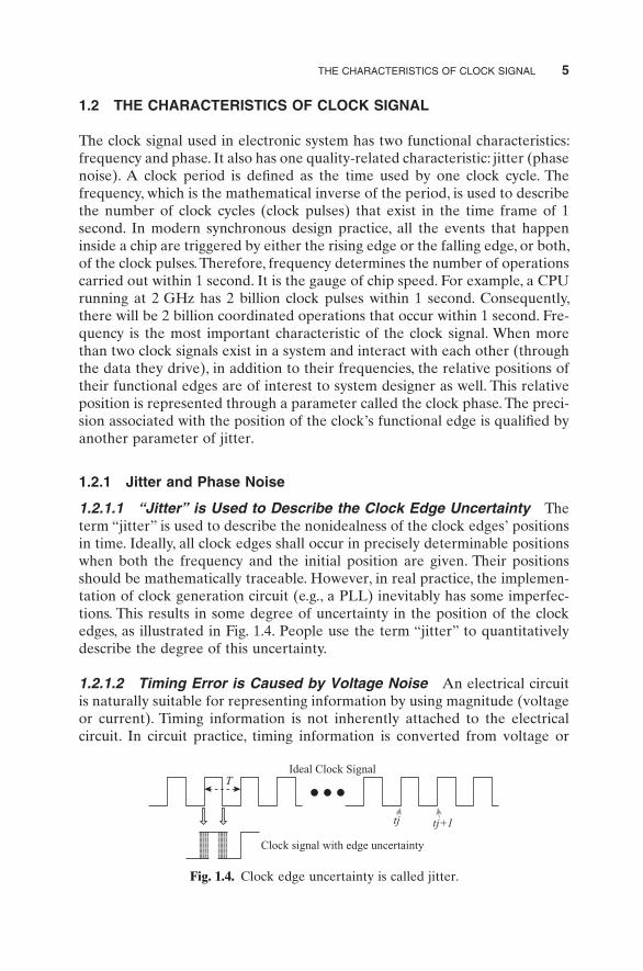
1.2.1.1 “ Jitter ” is Used to Describe the Clock Edge Uncertainty The term “ jitter ” is used to describe the nonidealness of the clock edges ’ positions in time. Ideally, all clock edges shall occur in precisely determinable positions when both the frequency and the initial position are given. Their positions should be mathematically traceable. However, in real practice, the implemen-tation of clock generation circuit (e.g., a PLL) inevitably has some imperfec-tions. This results in some degree of uncertainty in the position of the clock edges, as illustrated in Fig. 1.4 . People use the term “ jitter ” to quantitatively describe the degree of this uncertainty.
1.2.1.2 Timing Error is Caused by Voltage Noise An electrical circuit is naturally suitable for representing information by using magnitude (voltage or current). Timing information is not inherently attached to the electrical circuit. In circuit practice, timing information is converted from voltage or
Fig. 1.4. Clock edge uncertainty is called jitter.
Ideal Clock Signal
Clock signal with edge uncertainty
T
tj tj+1
6 CLOCK SIGNAL IN ELECTRONIC SYSTEMS
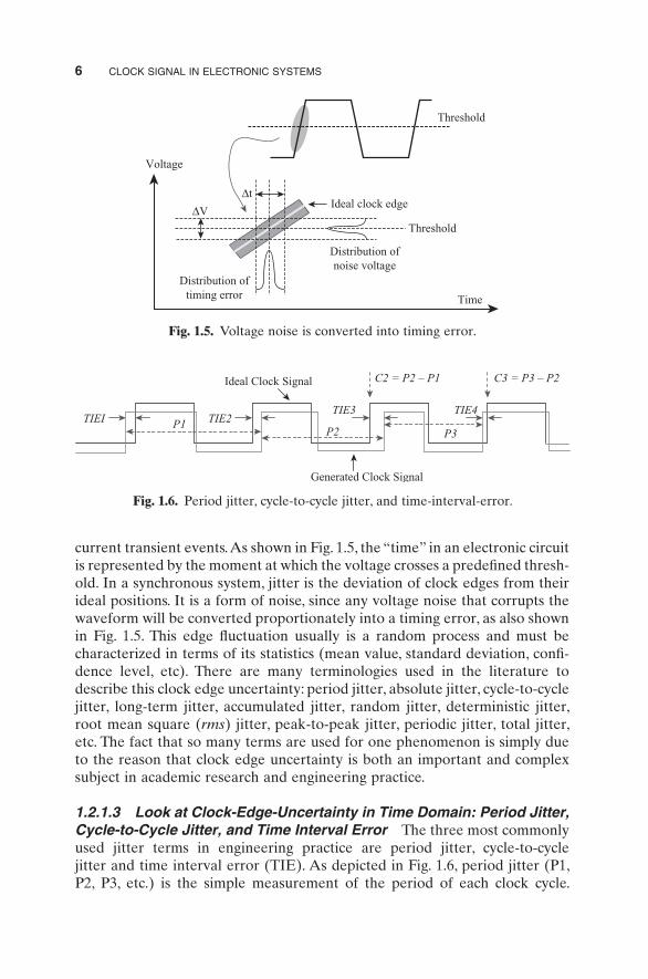
current transient events. As shown in Fig. 1.5 , the “ time ” in an electronic circuit is represented by the moment at which the voltage crosses a predefi ned thresh-old. In a synchronous system, jitter is the deviation of clock edges from their ideal positions. It is a form of noise, since any voltage noise that corrupts the waveform will be converted proportionately into a timing error, as also shown in Fig. 1.5 . This edge fl uctuation usually is a random process and must be characterized in terms of its statistics (mean value, standard deviation, confi -dence level, etc). There are many terminologies used in the literature to describe this clock edge uncertainty: period jitter, absolute jitter, cycle - to - cycle jitter, long - term jitter, accumulated jitter, random jitter, deterministic jitter, root mean square ( rms ) jitter, peak - to - peak jitter, periodic jitter, total jitter, etc. The fact that so many terms are used for one phenomenon is simply due to the reason that clock edge uncertainty is both an important and complex subject in academic research and engineering practice.
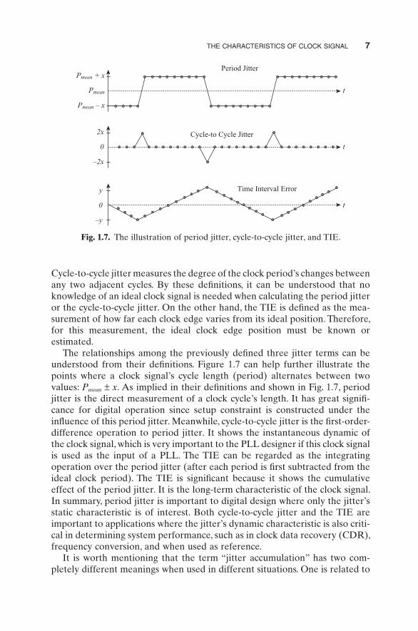
1.2.1.3 Look at Clock - Edge - Uncertainty in Time Domain: Period Jitter, Cycle - to - Cycle Jitter, and Time Interval Error The three most commonly used jitter terms in engineering practice are period jitter, cycle - to - cycle jitter and time interval error ( TIE ). As depicted in Fig. 1.6 , period jitter (P1, P2, P3, etc.) is the simple measurement of the period of each clock cycle.
Fig. 1.5. Voltage noise is converted into timing error.
Voltage
Distribution oftiming error
Distribution ofnoise voltage
Threshold
Time
Ideal clock edge
Threshold
∆V
∆t
Fig. 1.6. Period jitter, cycle - to - cycle jitter, and time - interval - error.
Ideal Clock Signal
TIEI
Generated Clock Signal
P1 TIE2P2
TIE3 TIE4
P3
C2 = P2 – P1 C3 = P3 – P2
THE CHARACTERISTICS OF CLOCK SIGNAL 7
Cycle - to - cycle jitter measures the degree of the clock period ’ s changes between any two adjacent cycles. By these defi nitions, it can be understood that no knowledge of an ideal clock signal is needed when calculating the period jitter or the cycle - to - cycle jitter. On the other hand, the TIE is defi ned as the mea-surement of how far each clock edge varies from its ideal position. Therefore, for this measurement, the ideal clock edge position must be known or estimated.
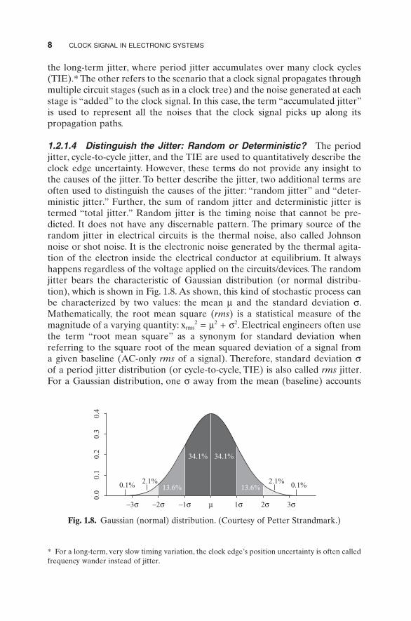
The relationships among the previously defi ned three jitter terms can be understood from their defi nitions. Figure 1.7 can help further illustrate the points where a clock signal ’ s cycle length (period) alternates between two values: P mean ± x . As implied in their defi nitions and shown in Fig. 1.7 , period jitter is the direct measurement of a clock cycle ’ s length. It has great signifi -cance for digital operation since setup constraint is constructed under the infl uence of this period jitter. Meanwhile, cycle - to - cycle jitter is the fi rst - order - difference operation to period jitter. It shows the instantaneous dynamic of the clock signal, which is very important to the PLL designer if this clock signal is used as the input of a PLL. The TIE can be regarded as the integrating operation over the period jitter (after each period is fi rst subtracted from the ideal clock period). The TIE is signifi cant because it shows the cumulative effect of the period jitter. It is the long - term characteristic of the clock signal. In summary, period jitter is important to digital design where only the jitter ’ s static characteristic is of interest. Both cycle - to - cycle jitter and the TIE are important to applications where the jitter ’ s dynamic characteristic is also criti-cal in determining system performance, such as in clock data recovery ( CDR ), frequency conversion, and when used as reference.
It is worth mentioning that the term “ jitter accumulation ” has two com-pletely different meanings when used in different situations. One is related to
Fig. 1.7. The illustration of period jitter, cycle - to - cycle jitter, and TIE.
Period Jitter
Cycle-to Cycle Jitter
Time Interval Error
t
t
t
Pmean + x
Pmean
Pmean – x
2x
0
–2x
y
0
–y
8 CLOCK SIGNAL IN ELECTRONIC SYSTEMS
the long - term jitter, where period jitter accumulates over many clock cycles (TIE). * The other refers to the scenario that a clock signal propagates through multiple circuit stages (such as in a clock tree) and the noise generated at each stage is “ added ” to the clock signal. In this case, the term “ accumulated jitter ” is used to represent all the noises that the clock signal picks up along its propagation paths.
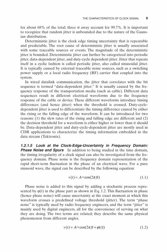
1.2.1.4 Distinguish the Jitter: Random or Deterministic? The period jitter, cycle - to - cycle jitter, and the TIE are used to quantitatively describe the clock edge uncertainty. However, these terms do not provide any insight to the causes of the jitter. To better describe the jitter, two additional terms are often used to distinguish the causes of the jitter: “ random jitter ” and “ deter-ministic jitter. ” Further, the sum of random jitter and deterministic jitter is termed “ total jitter. ” Random jitter is the timing noise that cannot be pre-dicted. It does not have any discernable pattern. The primary source of the random jitter in electrical circuits is the thermal noise, also called Johnson noise or shot noise. It is the electronic noise generated by the thermal agita-tion of the electron inside the electrical conductor at equilibrium. It always happens regardless of the voltage applied on the circuits/devices. The random jitter bears the characteristic of Gaussian distribution (or normal distribu-tion), which is shown in Fig. 1.8 . As shown, this kind of stochastic process can be characterized by two values: the mean μ and the standard deviation σ . Mathematically, the root mean square ( rms ) is a statistical measure of the magnitude of a varying quantity: x rms 2 = μ 2 + σ 2 . Electrical engineers often use the term “ root mean square ” as a synonym for standard deviation when referring to the square root of the mean squared deviation of a signal from a given baseline (AC - only rms of a signal). Therefore, standard deviation σ of a period jitter distribution (or cycle - to - cycle, TIE) is also called rms jitter. For a Gaussian distribution, one σ away from the mean (baseline) accounts
Fig. 1.8. Gaussian (normal) distribution. (Courtesy of Petter Strandmark.)
0.0
0.1
0.2
0.3
0.4
0.1% 0.1%2.1% 2.1%13.6%
34.1% 34.1%
µ 1σ 2σ 3σ–3σ –2σ –1σ
13.6%
* For a long - term, very slow timing variation, the clock edge ’ s position uncertainty is often called frequency wander instead of jitter.
THE CHARACTERISTICS OF CLOCK SIGNAL 9
for about 68% of the total; three σ away account for 99.7%. It is important to recognize that random jitter is unbounded due to the nature of the Gauss-ian distribution.
Deterministic jitter is the clock edge timing uncertainty that is repeatable and predictable. The root cause of deterministic jitter is usually associated with some traceable sources or events. The magnitude of the deterministic jitter is bounded. Deterministic jitter can further be categorized into periodic jitter, data - dependent jitter, and duty - cycle dependent jitter. Jitter that repeats itself in a cyclic fashion is called periodic jitter, also called sinusoidal jitter. It is typically caused by external traceable noise sources, such as a switching power supply or a local radio frequency (RF) carrier that coupled into the system.
In wired datalink communication, the jitter that correlates with the bit sequence is termed “ data - dependent jitter. ” It is usually caused by the fre-quency response of the transportation media (such as cable). Different data sequences result in different electrical waveforms due to the frequency response of the cable or device. These different waveforms introduce timing differences (and hence jitter) when the threshold is crossed. Duty - cycle - dependent jitter is used to differentiate the timing difference caused by either the rising or the falling edge of the waveform. It can be introduced for two reasons: (1) the slew rates of the rising and falling edge are different and (2) the decision threshold for a waveform is either higher or lower than it should be. Data - dependent jitter and duty - cycle - dependent jitter are mostly used in CDR applications to characterize the timing information embedded in the data stream (Tektronix).
1.2.1.5 Look at the Clock - Edge - Uncertainty in Frequency Domain: Phase Noise and Spurs In addition to being studied in the time domain, the timing irregularity of a clock signal can also be investigated from the fre-quency domain. Phase noise is the frequency domain representation of the rapid short - term fl uctuation in the phase of an electrical wave. For a pure sinusoid wave, the signal can be described by the following equation:
v t A ft( ) = ∗cos( )2π (1.1)
Phase noise is added to this signal by adding a stochastic process repre-sented by φ (t) in the phase part as shown in Eq. 1.2 . This fl uctuation in phase (hence phase noise) will cause uncertainty at the exact moment at which this waveform crosses a predefi ned voltage threshold (jitter). The term “ phase noise ” is typically used by radio frequency engineers, and the term “ jitter ” is mainly used by digital engineers, all for the convenience of serving on what they are doing. The two terms are related; they describe the same physical phenomenon from different angles.
v t A ft t( ) = ∗ +cos( ( ))2π ϕ (1.2)
10 CLOCK SIGNAL IN ELECTRONIC SYSTEMS
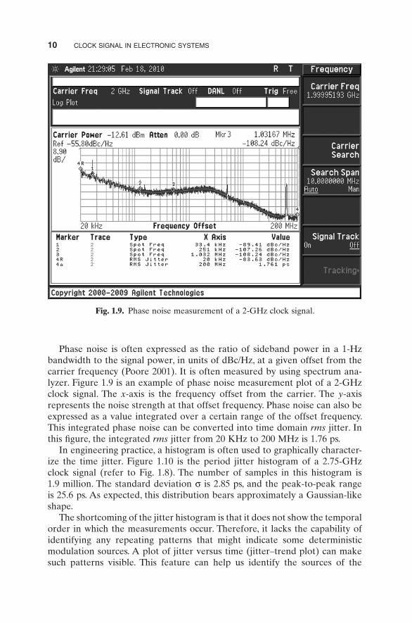
Phase noise is often expressed as the ratio of sideband power in a 1 - Hz bandwidth to the signal power, in units of dBc/Hz, at a given offset from the carrier frequency (Poore 2001 ). It is often measured by using spectrum ana-lyzer. Figure 1.9 is an example of phase noise measurement plot of a 2 - GHz clock signal. The x - axis is the frequency offset from the carrier. The y - axis represents the noise strength at that offset frequency. Phase noise can also be expressed as a value integrated over a certain range of the offset frequency. This integrated phase noise can be converted into time domain rms jitter. In this fi gure, the integrated rms jitter from 20 KHz to 200 MHz is 1.76 ps.
In engineering practice, a histogram is often used to graphically character-ize the time jitter. Figure 1.10 is the period jitter histogram of a 2.75 - GHz clock signal (refer to Fig. 1.8 ). The number of samples in this histogram is 1.9 million. The standard deviation σ is 2.85 ps, and the peak - to - peak range is 25.6 ps. As expected, this distribution bears approximately a Gaussian - like shape.
The shortcoming of the jitter histogram is that it does not show the temporal order in which the measurements occur. Therefore, it lacks the capability of identifying any repeating patterns that might indicate some deterministic modulation sources. A plot of jitter versus time (jitter – trend plot) can make such patterns visible. This feature can help us identify the sources of the
Fig. 1.9. Phase noise measurement of a 2 - GHz clock signal.

THE CHARACTERISTICS OF CLOCK SIGNAL 11
disturbances. The extension of this jitter - vs - time measurement is to apply fast Fourier transform ( FFT ) to it. The result, displayed in the frequency domain, is the jitter spectrum. The benefi t of jitter spectral analysis is that any periodic components (periodic jitter) embedded in the noise can potentially be distinguished. Hence, the triggering source could be identifi ed. Figure 1.11 shows one such jitter spectrum plot. * Clearly, there is a 15 - KHz fundamental
Fig. 1.10. The period jitter histogram of a 2.75 - GHz clock signal.
Fig. 1.11. The jitter spectrum plot.
10ns
100ps
1ps
10fs
1kHz 10kHz
Y:Time TIE1:Spectrum X:Freq
–1
100kHz 1MHz 10MHz 100MHz
* Borrowed from Tektronix.
12 CLOCK SIGNAL IN ELECTRONIC SYSTEMS
frequency in the noises. The second (30 KHz), and third (45 KHz) harmonics can also be seen easily. This suggests that a 15 - KHz nearby signal could be coupled into the clock signal.
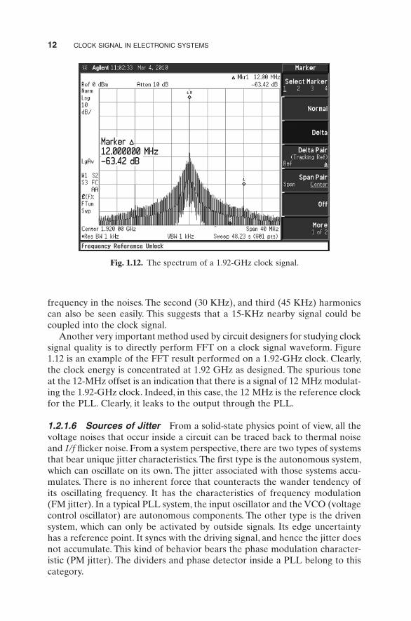
Another very important method used by circuit designers for studying clock signal quality is to directly perform FFT on a clock signal waveform. Figure 1.12 is an example of the FFT result performed on a 1.92 - GHz clock. Clearly, the clock energy is concentrated at 1.92 GHz as designed. The spurious tone at the 12 - MHz offset is an indication that there is a signal of 12 MHz modulat-ing the 1.92 - GHz clock. Indeed, in this case, the 12 MHz is the reference clock for the PLL. Clearly, it leaks to the output through the PLL.
1.2.1.6 Sources of Jitter From a solid - state physics point of view, all the voltage noises that occur inside a circuit can be traced back to thermal noise and 1/f fl icker noise. From a system perspective, there are two types of systems that bear unique jitter characteristics. The fi rst type is the autonomous system, which can oscillate on its own. The jitter associated with those systems accu-mulates. There is no inherent force that counteracts the wander tendency of its oscillating frequency. It has the characteristics of frequency modulation (FM jitter). In a typical PLL system, the input oscillator and the VCO ( voltage control oscillator ) are autonomous components. The other type is the driven system, which can only be activated by outside signals. Its edge uncertainty has a reference point. It syncs with the driving signal, and hence the jitter does not accumulate. This kind of behavior bears the phase modulation character-istic (PM jitter). The dividers and phase detector inside a PLL belong to this category.
Fig. 1.12. The spectrum of a 1.92 - GHz clock signal.
THE CHARACTERISTICS OF CLOCK SIGNAL 13
When an electronic system is investigated as a whole, components that can contribute to total jitter though jitter accumulation are as follows:
• all transistors used in the circuit • all passive components (resistor, capacitor, and inductor) used in the
circuit • random thermal and mechanical noise from crystal • parasitic components from signal interconnections (within the integrated
circuit [IC]) • trace, cable, and connector used in the printed circuit board (PCB) level.
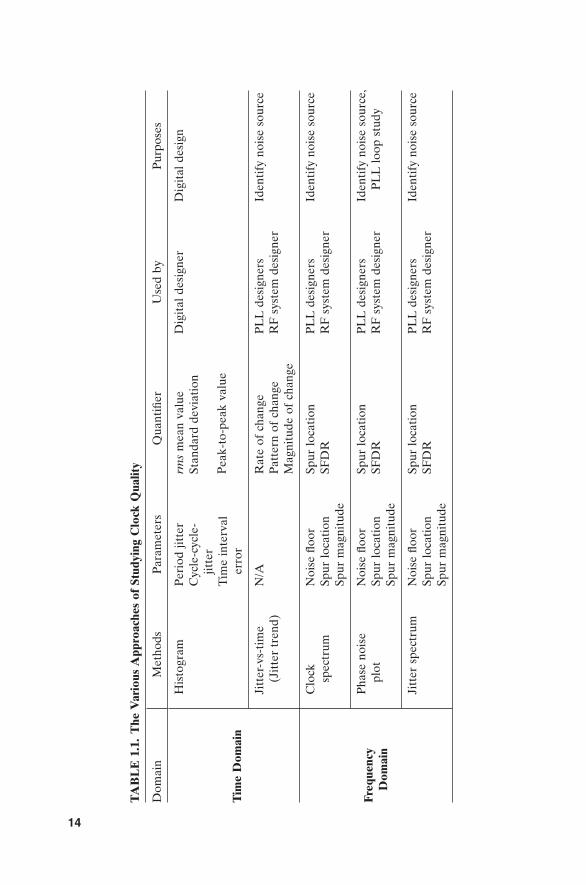
1.2.1.7 Summary Table 1.1 lists all the methods for studying clock quality. They are different ways of looking at the same thing: clock edge uncertainty. Digital designers prefer to use the term “ jitter ” while RF designers typically use the term “ phase noise. ” They are related and can be converted to/from each other. When clock edge uncertainty is caused by stochastic processes, its distribution in the time domain histogram is Gaussian - like. In the frequency domain, it raises the noise fl oor. When clock edge uncertainty is sourced from periodic events, spurs (spurious tones) appear in its frequency spectrum. In the time domain, its histogram will deviate from Gaussian distribution because of those periodic events.
1.2.2 Clock Phase
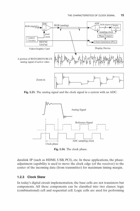
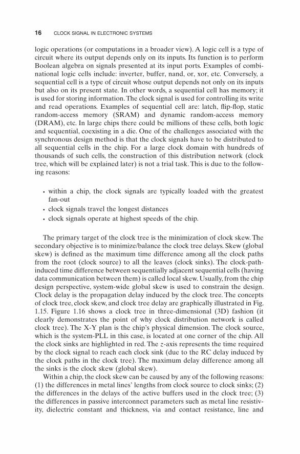
When a clock signal is used to drive an analog - to - digital converter ( ADC ), another clock characteristic called clock phase is important. An example is shown in Fig. 1.13 . In this system, an analog signal and a clock signal are trans-mitted from transmitter to receiver through different cables. Thus, they experi-ence different delays. Moreover, the analog signal is originated from a digital - to - analog converter ( DAC ). There is an area of overshoot and ringing within each data boundary. Clearly, on the receiving side, the exact moment at which the ADC takes the sample has great impact on the value converted. It is desirable that some tuning capability is available inside the receiving side ’ s clock circuitry so that the position of the clock edge that will trigger the ADC can be adjusted. Within such a system, the exact sampling moment is called the clock phase, as illustrated in Fig. 1.14 . In this scenario, phase is proportional to time. Different phases correspond to different time delays from a reference point. In many such systems, there could be 4, 8, 16, or 32 phases available within one clock cycle to help achieve the optimal result.
Clock phase is also important in digital communication when data are moved between blocks, modules, and chips. In such applications, information is exchanged between different domains, and each domain has its own clock. The relative position of the clock edges, which is represented using the clock phase of one of the involved clocks, plays a crucial role in the success of the data transfer. Examples include double data rate (DDR) memory interface,
TAB
LE
1.1
. T
he V
ario
us A
ppro
ache
s of
Stu
dyin
g C
lock
Qua
lity
Dom
ain
Met
hods
P
aram
eter
s Q
uant
ifi er
U
sed
by
Pur
pose
s
Tim
e D
omai
n
His
togr
am
Per
iod
jitte
r C
ycle
- cyc
le -
jitte
r T
ime
inte
rval
er
ror
rms
mea
n va
lue
Stan
dard
dev
iati
on
Pea
k - to
- pea
k va
lue
Dig
ital
des
igne
r D
igit
al d
esig
n
Jitt
er - v
s - ti
me
(Jit
ter
tren
d)
N/A
R
ate
of c
hang
e P
atte
rn o
f ch
ange
M
agni
tude
of
chan
ge
PL
L d
esig
ners
R
F s
yste
m d
esig
ner
Iden
tify
noi
se s
ourc
e
Freq
uenc
y D
omai
n
Clo
ck
spec
trum
N
oise
fl oo
r Sp
ur lo
cati
on
Spur
mag
nitu
de
Spur
loca
tion
SF
DR
P
LL
des
igne
rs
RF
sys
tem
des
igne
r Id
enti
fy n
oise
sou
rce
Pha
se n
oise
pl
ot
Noi
se fl
oor
Spur
loca
tion
Sp
ur m
agni
tude
Spur
loca
tion
SF
DR
P
LL
des
igne
rs
RF
sys
tem
des
igne
r Id
enti
fy n
oise
sou
rce,
P
LL
loop
stu
dy
Jitt
er s
pect
rum
N
oise
fl oo
r Sp
ur lo
cati
on
Spur
mag
nitu
de
Spur
loca
tion
SF
DR
P
LL
des
igne
rs
RF
sys
tem
des
igne
r Id
enti
fy n
oise
sou
rce
14
THE CHARACTERISTICS OF CLOCK SIGNAL 15
datalink IP (such as HDMI, USB, PCI), etc. In these applications, the phase - adjustment capability is used to move the clock edge (of the receiver) to the center of the incoming data (from transmitter) for maximum timing margin.
1.2.3 Clock Skew
In today ’ s digital circuit implementation, the base cells are not transistors but components. All these components can be classifi ed into two classes: logic (combinational) cell and sequential cell. Logic cells are used for performing
Fig. 1.13. The analog signal and the clock signal in a system with an ADC.
RGB (digital)3RGB (digital)
3
ControlCircuitry
HSYNCVSYNC
Video/Graphic Card
DAC
pixelclock
RGB (analog)
A portion of RED/GREEN/BLUEanalog signal of active video
Zoom-in
ADCDisplayCircuitry
sampling clock
Phase Control
Clock Generation (PLL)
Display Device
Fig. 1.14. The clock phase.
Analog Signal
Reference Signal
Clock phaseADC sampling clock
16 CLOCK SIGNAL IN ELECTRONIC SYSTEMS
logic operations (or computations in a broader view). A logic cell is a type of circuit where its output depends only on its inputs. Its function is to perform Boolean algebra on signals presented at its input ports. Examples of combi-national logic cells include: inverter, buffer, nand, or, xor, etc. Conversely, a sequential cell is a type of circuit whose output depends not only on its inputs but also on its present state. In other words, a sequential cell has memory; it is used for storing information. The clock signal is used for controlling its write and read operations. Examples of sequential cell are: latch, fl ip - fl op, static random - access memory (SRAM) and dynamic random - access memory (DRAM), etc. In large chips there could be millions of these cells, both logic and sequential, coexisting in a die. One of the challenges associated with the synchronous design method is that the clock signals have to be distributed to all sequential cells in the chip. For a large clock domain with hundreds of thousands of such cells, the construction of this distribution network (clock tree, which will be explained later) is not a trial task. This is due to the follow-ing reasons:
• within a chip, the clock signals are typically loaded with the greatest fan - out
• clock signals travel the longest distances • clock signals operate at highest speeds of the chip.
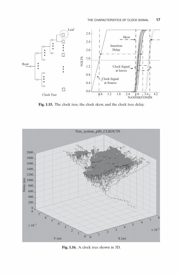
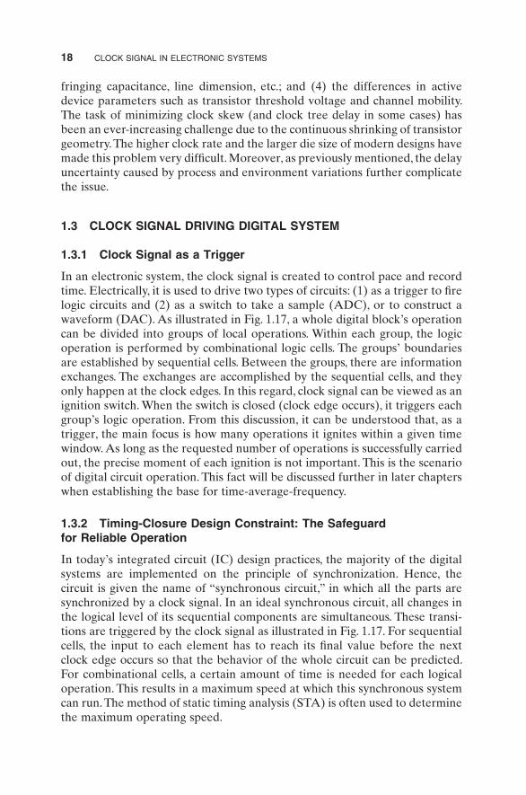
The primary target of the clock tree is the minimization of clock skew. The secondary objective is to minimize/balance the clock tree delays. Skew (global skew) is defi ned as the maximum time difference among all the clock paths from the root (clock source) to all the leaves (clock sinks). The clock - path - induced time difference between sequentially adjacent sequential cells (having data communication between them) is called local skew. Usually, from the chip design perspective, system - wide global skew is used to constrain the design. Clock delay is the propagation delay induced by the clock tree. The concepts of clock tree, clock skew, and clock tree delay are graphically illustrated in Fig. 1.15 . Figure 1.16 shows a clock tree in three - dimensional (3D) fashion (it clearly demonstrates the point of why clock distribution network is called clock tree). The X - Y plan is the chip ’ s physical dimension. The clock source, which is the system - PLL in this case, is located at one corner of the chip. All the clock sinks are highlighted in red. The z - axis represents the time required by the clock signal to reach each clock sink (due to the RC delay induced by the clock paths in the clock tree). The maximum delay difference among all the sinks is the clock skew (global skew).
Within a chip, the clock skew can be caused by any of the following reasons: (1) the differences in metal lines ’ lengths from clock source to clock sinks; (2) the differences in the delays of the active buffers used in the clock tree; (3) the differences in passive interconnect parameters such as metal line resistiv-ity, dielectric constant and thickness, via and contact resistance, line and
THE CHARACTERISTICS OF CLOCK SIGNAL 17
Fig. 1.15. The clock tree, the clock skew, and the clock tree delay.
Clock Tree
Root
Leaf
VO
LTS
2.8
2.4
2.0
1.6
1.2
0.8
0.4
0.0
Clock Signalat leaves
Clock Signalat Source
InsertionDelay
Skew
0.6 1.2 1.8 2.4 3.0 3.6 4.2NANOSECONDS
Fig. 1.16. A clock tree shown in 3D.
Tree_system_pll0_CLKOUT0
Del
ay (
ps)
Y (m) X (m)
× 10–3
× 10–3
2000
1800
1600
1400
1200
1000
800
600
400
200
08
76
54
32
10
87
65
43
21
0
18 CLOCK SIGNAL IN ELECTRONIC SYSTEMS
fringing capacitance, line dimension, etc.; and (4) the differences in active device parameters such as transistor threshold voltage and channel mobility. The task of minimizing clock skew (and clock tree delay in some cases) has been an ever - increasing challenge due to the continuous shrinking of transistor geometry. The higher clock rate and the larger die size of modern designs have made this problem very diffi cult. Moreover, as previously mentioned, the delay uncertainty caused by process and environment variations further complicate the issue.
1.3 CLOCK SIGNAL DRIVING DIGITAL SYSTEM
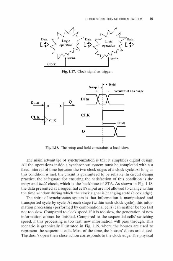
1.3.1 Clock Signal as a Trigger
In an electronic system, the clock signal is created to control pace and record time. Electrically, it is used to drive two types of circuits: (1) as a trigger to fi re logic circuits and (2) as a switch to take a sample (ADC), or to construct a waveform (DAC). As illustrated in Fig. 1.17 , a whole digital block ’ s operation can be divided into groups of local operations. Within each group, the logic operation is performed by combinational logic cells. The groups ’ boundaries are established by sequential cells. Between the groups, there are information exchanges. The exchanges are accomplished by the sequential cells, and they only happen at the clock edges. In this regard, clock signal can be viewed as an ignition switch. When the switch is closed (clock edge occurs), it triggers each group ’ s logic operation. From this discussion, it can be understood that, as a trigger, the main focus is how many operations it ignites within a given time window. As long as the requested number of operations is successfully carried out, the precise moment of each ignition is not important. This is the scenario of digital circuit operation. This fact will be discussed further in later chapters when establishing the base for time - average - frequency.
1.3.2 Timing - Closure Design Constraint: The Safeguard for Reliable Operation
In today ’ s integrated circuit (IC) design practices, the majority of the digital systems are implemented on the principle of synchronization. Hence, the circuit is given the name of “ synchronous circuit, ” in which all the parts are synchronized by a clock signal. In an ideal synchronous circuit, all changes in the logical level of its sequential components are simultaneous. These transi-tions are triggered by the clock signal as illustrated in Fig. 1.17 . For sequential cells, the input to each element has to reach its fi nal value before the next clock edge occurs so that the behavior of the whole circuit can be predicted. For combinational cells, a certain amount of time is needed for each logical operation. This results in a maximum speed at which this synchronous system can run. The method of static timing analysis ( STA ) is often used to determine the maximum operating speed.
CLOCK SIGNAL DRIVING DIGITAL SYSTEM 19
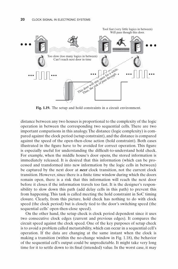
The main advantage of synchronization is that it simplifi es digital design. All the operations inside a synchronous system must be completed within a fi xed interval of time between the two clock edges of a clock cycle. As long as this condition is met, the circuit is guaranteed to be reliable. In circuit design practice, the safeguard for ensuring the satisfaction of this condition is the setup and hold check, which is the backbone of STA. As shown in Fig. 1.18 , the data presented at a sequential cell ’ s input are not allowed to change within the time window during which the clock signal is changing state (clock edge).
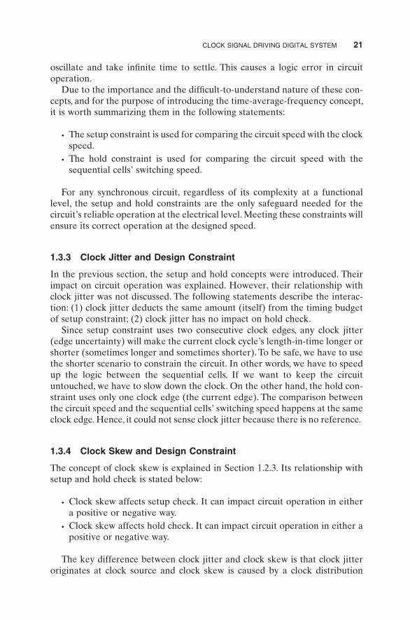
The spirit of synchronous system is that information is manipulated and transported cycle by cycle. At each stage (within each clock cycle), this infor-mation processing (performed by combinational cells) can neither be too fast not too slow. Compared to clock speed, if it is too slow, the generation of new information cannot be fi nished. Compared to the sequential cells ’ switching speed, if this processing is too fast, new information will pass through. This scenario is graphically illustrated in Fig. 1.19 , where the houses are used to represent the sequential cells. Most of the time, the houses ’ doors are closed. The door ’ s open - then - close action corresponds to the clock edge. The physical
Fig. 1.17. Clock signal as trigger.
Fig. 1.18. The setup and hold constraints: a local view.
20 CLOCK SIGNAL IN ELECTRONIC SYSTEMS
distance between any two houses is proportional to the complexity of the logic operation in between the corresponding two sequential cells. There are two important comparisons in this analogy. The distance (logic complexity) is com-pared against the clock period (setup constraint), and the distance is compared against the speed of the open - then - close action (hold constraint). Both cases illustrated in the fi gure have to be avoided for correct operation. This fi gure is especially useful for understanding the diffi cult - to - understand hold check. For example, when the middle house ’ s door opens, the stored information is immediately released. It is desired that this information (which can be pro-cessed and transformed into new information by the logic cells in between) be captured by the next door at next clock transition, not the current clock transition. However, since there is a fi nite time window during which the doors remain open, there is a risk that this information will reach the next door before it closes if the information travels too fast. It is the designer ’ s respon-sibility to slow down this path (add delay cells in this path) to prevent this from happening. This task is called meeting the hold constraint in SoC timing closure. Clearly, from this picture, hold check has nothing to do with clock speed (the clock period) but is closely tied to the door ’ s switching speed (the sequential cells ’ open - then - close speed).
On the other hand, the setup check is clock period dependent since it uses two consecutive clock edges (current and previous edges). It compares the circuit speed against the clock speed. One of the key purposes of setup check is to avoid a problem called metastability, which can occur in a sequential cell ’ s operation. If the data are changing at the same instant when the clock is making a transition (within the no - change window in Fig. 1.18 ), the behavior of the sequential cell ’ s output could be unpredictable. It might take very long time for it to settle down to its fi nal (intended) value. In the worst case, it may
Fig. 1.19. The setup and hold constraints in a circuit environment.
Too slow (too many logics in between)Can’t reach next door in time
Tool fast (very little logics in between)Will pass though this door.
This door w
ill sta
y open for a while.
Thus, the ris
k of pass t
hrough.
CLOCK SIGNAL DRIVING DIGITAL SYSTEM 21
oscillate and take infi nite time to settle. This causes a logic error in circuit operation.
Due to the importance and the diffi cult - to - understand nature of these con-cepts, and for the purpose of introducing the time - average - frequency concept, it is worth summarizing them in the following statements:
• The setup constraint is used for comparing the circuit speed with the clock speed.
• The hold constraint is used for comparing the circuit speed with the sequential cells ’ switching speed.
For any synchronous circuit, regardless of its complexity at a functional level, the setup and hold constraints are the only safeguard needed for the circuit ’ s reliable operation at the electrical level. Meeting these constraints will ensure its correct operation at the designed speed.
1.3.3 Clock Jitter and Design Constraint
In the previous section, the setup and hold concepts were introduced. Their impact on circuit operation was explained. However, their relationship with clock jitter was not discussed. The following statements describe the interac-tion: (1) clock jitter deducts the same amount (itself) from the timing budget of setup constraint; (2) clock jitter has no impact on hold check.
Since setup constraint uses two consecutive clock edges, any clock jitter (edge uncertainty) will make the current clock cycle ’ s length - in - time longer or shorter (sometimes longer and sometimes shorter). To be safe, we have to use the shorter scenario to constrain the circuit. In other words, we have to speed up the logic between the sequential cells. If we want to keep the circuit untouched, we have to slow down the clock. On the other hand, the hold con-straint uses only one clock edge (the current edge). The comparison between the circuit speed and the sequential cells ’ switching speed happens at the same clock edge. Hence, it could not sense clock jitter because there is no reference.
1.3.4 Clock Skew and Design Constraint
The concept of clock skew is explained in Section 1.2.3 . Its relationship with setup and hold check is stated below:
• Clock skew affects setup check. It can impact circuit operation in either a positive or negative way.
• Clock skew affects hold check. It can impact circuit operation in either a positive or negative way.
The key difference between clock jitter and clock skew is that clock jitter originates at clock source and clock skew is caused by a clock distribution

22 CLOCK SIGNAL IN ELECTRONIC SYSTEMS
network (clock tree). Since jitter is initiated at the source, all the sequential cells (clock sinks) attached to this source sense the same impact. Skew is caused by the physical distribution network; each individual clock sink feels a different impact owing to its unique path. (Refer to Fig. 1.20 where there are a group of sequential cells attached to a clock source.) The clock signal from the source is distributed to all the sequential cells through the clock tree; each cell has its own unique physical distribution path and thus unique timing delay associated with it. We use cell #1 and cell #2 to illustrate the interaction between clock skew and design constraint.
For this investigation, there are two clock edges and two cells involved: the current clock edge and the previous clock edge, the launching cell (the cell that launches data), and the receiving cell (the cell that receives data). The follow-ing is the list of symbols that we will use for discussion (refer to Fig. 1.20 ).
t c : the moment that current clock edge emerges from the clock source t p : the moment that previous clock edge emerges from the clock source t 1 c : the moment that current clock edge reaches cell #1, the launching
cell t 1 p : the moment that previous clock edge reaches cell #1 t 2 c : the moment that current clock edge reaches cell #2, the receiving cell t 2 p : the moment that previous clock edge reaches cell #2 t skew : t skew = t delay 2 − t delay 1
By defi nition, we have
t t Tc p− = (1.3)
t t t t t tc c delay p p delay1 1 1 1= + = +, (1.4)
Fig. 1.20. Clock skew and design constraints.

CLOCK SIGNAL DRIVING DIGITAL SYSTEM 23
t t t t t tc c delay p p delay2 2 2 2= + = +, (1.5)
For a setup check, data are launched from cell #1 at the previous edge. They are received at cell #2 at the current edge. Therefore, the impact of skew on the timing budget (allocated for logic operation in between the two adjacent sequential cells), t s_delta , is calculated in Eq. 1.6 .
t t t t t t t T ts delta c p c delay p delay skew_ = − = + − − = +2 1 2 1 (1.6)
For the hold constraint, instead of the previous edge, data are launched from cell #1 at the current edge. They are received at cell #2, also at the current edge. Thus, the skew ’ s impact on timing budget t h_delta can be expressed in Eq. 1.7 :
t t t t t t t th delta c c c delay c delay skew_ = − = + − − =2 1 2 1 (1.7)
From Eqs. 1.6 and 1.7 , it is clear that clock skew t skew has an impact on both the setup and hold checks. Depending on the sign of t skew , it can play a positive or negative role in circuit operation. For example, when t skew is positive ( t delay 2 is larger than t delay 1 ), the current clock edge will arrive at cell #2 later than scheduled. This gives more time for the logic operation to be performed between cell #1 and cell #2. It eases the setup check. On the other hand, since the current clock edge arrives later than scheduled, cell #2 will consequently close its door later than normal. This fact increases the risk of data pass through for the data launched from cell #1 at the current edge. In other words, it makes it more diffi cult to satisfy the hold constraint. In the case where t skew is negative, a similar analysis can be carried out.
In the above analysis, the clock source is assumed to be ideal since t c − t p = T . If clock jitter is included, Eq. 1.3 would be modifi ed to t c − t p = T + t jitter , where t jitter is the amount of clock jitter. And Eq. 1.6 needs to be revised as t s_delta = T + t jitter + t skew . From here, it is clear that jitter has impact on the setup check as stated in the previous section. From Eq. 1.7 , however, the hold check is not related to clock period T. This explains why the hold check is not clock speed dependent.
Since the concepts of jitter, skew, setup, and hold are important and their relationship to clock frequency is diffi cult to be understood, Table 1.2 is created for reference. This understanding is crucial for the time - average - frequency concept that will be introduced in later chapters.
TABLE 1.2. Jitter, Skew and Setup, Hold Check
Cause
Impact on setup check (current and
previous edge)
Impact on hold check
(current edge)
Jitter Clock source (PLL/DLL) Yes No Skew Physical distribution path Yes Yes
24 CLOCK SIGNAL IN ELECTRONIC SYSTEMS
1.4 CLOCK SIGNAL DRIVING SAMPLING SYSTEM
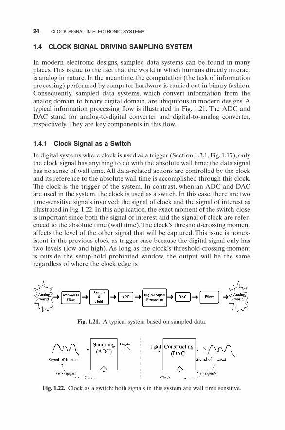
In modern electronic designs, sampled data systems can be found in many places. This is due to the fact that the world in which humans directly interact is analog in nature. In the meantime, the computation (the task of information processing) performed by computer hardware is carried out in binary fashion. Consequently, sampled data systems, which convert information from the analog domain to binary digital domain, are ubiquitous in modern designs. A typical information processing fl ow is illustrated in Fig. 1.21 . The ADC and DAC stand for analog - to - digital converter and digital - to - analog converter, respectively. They are key components in this fl ow.
1.4.1 Clock Signal as a Switch
In digital systems where clock is used as a trigger (Section 1.3.1 , Fig. 1.17 ), only the clock signal has anything to do with the absolute wall time; the data signal has no sense of wall time. All data - related actions are controlled by the clock and its reference to the absolute wall time is accomplished through this clock. The clock is the trigger of the system. In contrast, when an ADC and DAC are used in the system, the clock is used as a switch. In this case, there are two time - sensitive signals involved: the signal of clock and the signal of interest as illustrated in Fig. 1.22 . In this application, the exact moment of the switch - close is important since both the signal of interest and the signal of clock are refer-enced to the absolute time (wall time). The clock ’ s threshold - crossing moment affects the level of the other signal that will be captured. This issue is nonex-istent in the previous clock - as - trigger case because the digital signal only has two levels (low and high). As long as the clock ’ s threshold - crossing - moment is outside the setup - hold prohibited window, the output will be the same regardless of where the clock edge is.
Fig. 1.21. A typical system based on sampled data.
Fig. 1.22. Clock as a switch: both signals in this system are wall time sensitive.
CLOCK SIGNAL DRIVING SAMPLING SYSTEM 25
In this clock - as - switch application, the issue of the clock - affecting signal cannot be analyzed easily in the time domain. Short - term behavior alone is unable to provide clear picture. The study must be further carried out in long - term fashion. Hence, this subject is often investigated in the frequency domain. The clock spectral purity is of high concern.
1.4.2 Clock Signal and Analog - to - Digital Converter
The ADC is an important component for a signal processing system. There are two key concepts involved in the actual ADC conversion process: discrete time sampling and fi nite amplitude resolution (quantization). In implementa-tion, there are many varieties in ADC architecture. However, the ADC ’ s performance can be summarized by a relatively small number of parameters: resolution (number of bits per sample), signal - to - noise ratio ( SNR ), spurious - free dynamic range ( SFDR ), and power dissipation. The noise spectrum that affects the ADC performance contains contributions from such mechanisms as quantization noise, thermal noise, comparator ambiguity, and aperture jitter (aperture uncertainty). Among these, the aperture jitter, which is defi ned as a sample - to - sample variation of the instant at which the sampling operation occurs (switch - close), has great impact on SNR, SFDR, and ENOB ( effective number of bits ).
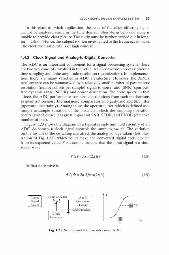
Figure 1.23 shows the diagram of a typical sample and hold circuitry of an ADC. As shown, a clock signal controls the sampling switch. The variation on the instant of the switching can affect the analog voltage taken (left illus-tration of Fig. 1.23 ), which could make the converted digital code deviate from its expected value. For example, assume that the input signal is a sinu-soidal wave
V t Asin ft( ) = ( )2π (1.8)
Its fi rst derivative is
dV dt Afcos ft= 2 2π π( ) (1.9)
Fig. 1.23. Sample and hold circuitry in an ADC.
Sample SwitchAnalogSignalSource
ClockGenerator
A to DConversion
Circuit
Hold Capacitor
V
t
∆V
∆t
26 CLOCK SIGNAL IN ELECTRONIC SYSTEMS
Therefore, the maximum time - error - introduced magnitude error occurs when cos (2 π ft ) = 1 and dv / dt = 2 π Af . Conceptually, if dt is the aperture jitter t a , dV is the error in the sampled voltage, which is termed V e . Then, we have
V Afte a= 2π (1.10)
This simple model indicates that the sampling voltage error increases lin-early both with the input signal ’ s frequency and the size of the jitter. The SNR can also be calculated from this simple model:
SNRAV
fte
a=
= −20 20 2log log( )π (1.11)
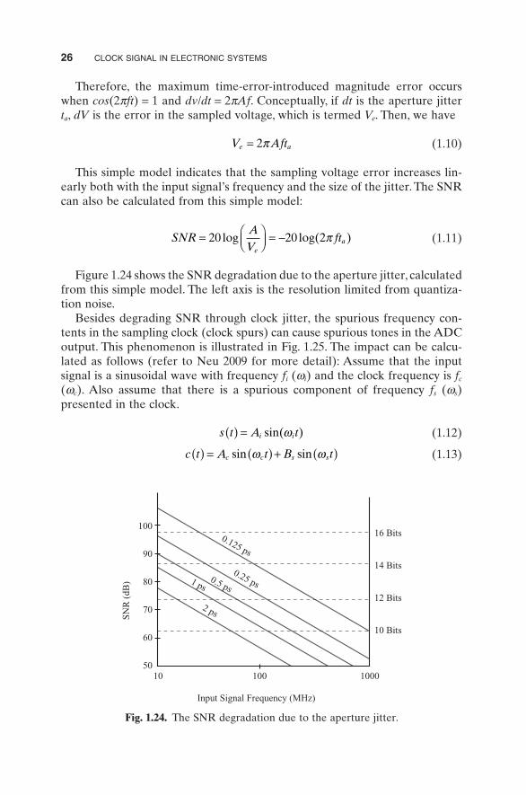
Figure 1.24 shows the SNR degradation due to the aperture jitter, calculated from this simple model. The left axis is the resolution limited from quantiza-tion noise.
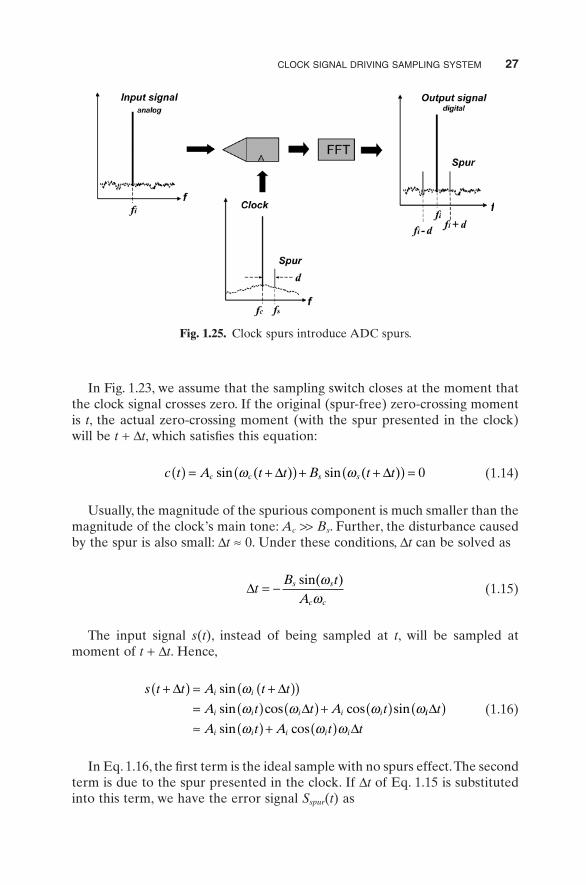
Besides degrading SNR through clock jitter, the spurious frequency con-tents in the sampling clock (clock spurs) can cause spurious tones in the ADC output. This phenomenon is illustrated in Fig. 1.25 . The impact can be calcu-lated as follows (refer to Neu 2009 for more detail): Assume that the input signal is a sinusoidal wave with frequency f i ( ω i ) and the clock frequency is f c ( ω c ). Also assume that there is a spurious component of frequency f s ( ω s ) presented in the clock.
s t A ti i( ) = sin( )ω (1.12)
c t A t B tc c s s( ) = ( ) + ( )sin sinω ω (1.13)
Fig. 1.24. The SNR degradation due to the aperture jitter.
SN
R (
dB)
Input Signal Frequency (MHz)
16 Bits
14 Bits
12 Bits
10 Bits
100
90
80
70
60
5010 100 1000
0.125 ps
0.25 ps0.5 ps1 ps
2 ps
CLOCK SIGNAL DRIVING SAMPLING SYSTEM 27
In Fig. 1.23 , we assume that the sampling switch closes at the moment that the clock signal crosses zero. If the original (spur - free) zero - crossing moment is t , the actual zero - crossing moment (with the spur presented in the clock) will be t + Δ t , which satisfi es this equation:
c t A t t B t tc c s s( ) = +( ) + +( ) =sin ( ) sin ( )ω ω∆ ∆ 0 (1.14)
Usually, the magnitude of the spurious component is much smaller than the magnitude of the clock ’ s main tone: A c >> B s . Further, the disturbance caused by the spur is also small: Δ t ≈ 0. Under these conditions, Δ t can be solved as
∆tB t
As s
c c
= −sin( )ω
ω (1.15)
The input signal s ( t ), instead of being sampled at t , will be sampled at moment of t + Δ t . Hence,
s t t A t t
A t t A ti i
i i i i i
+( ) = +( )( )= ( ) ( ) + ( )
∆ ∆∆
sin
sin cos cos sin
ωω ω ω ω ii
i i i i i
t
A t A t t
∆∆
( )≈ ( ) + ( )sin cosω ω ω
(1.16)
In Eq. 1.16 , the fi rst term is the ideal sample with no spurs effect. The second term is due to the spur presented in the clock. If Δ t of Eq. 1.15 is substituted into this term, we have the error signal S spur ( t ) as
Fig. 1.25. Clock spurs introduce ADC spurs.
28 CLOCK SIGNAL IN ELECTRONIC SYSTEMS
S t A tB t
A
ABA
spur i i is s
c c
is i
c c
( ) = ( )
=
cossin( )
sin[(
ω ω ωω
ωω2
−− + + − −{ }ω ω ω ωs i s it cos t) ] [( ) ] (1.17)
Compared with Eq. 1.12 , the scaling factor of error signal is B As i c cω ω2 = B f A fs i c c2 . Thus, its magnitude increases linearly both with the input fre-quency f i and the magnitude - of - clock - spur B s . If expressed in decibels, the magnitude can be shown as
Mag S B A f fspur s c i c( ) log[ / ( )]= − + 20 2 (1.18)
The spur locations are at − ω s + ω i and − ω s − ω i , or f s 1 = − f s + f i and f s 2 = − f s − f i . We can move the clock spur f s by multiples of clock f c . In other words, if there is a clock spur at − f s , we can also fi nd spurs at − f s + f c . Therefore, Eq. 1.19 can be derived where d is used to represent the distance between the clock ’ s main tone and its spur: d = f s − f c .
f f f f f f f f d f d
f f f f f fS s i c i s c i i
S s i c i s
1
2
= − − + = − + −( ) = − +( ) = += − + + = − + ff f d f dc i i( ) = −( ) = −
(1.19)
When the clock spur is far away from the clock ’ s main tone, the FFT plot of the ADC output can be confused if care is not taken. In these cases, the generated ADC spurs can be pushed outside the plot boundaries, either to the negative side or beyond the f c /2. The spurs will be aliased back and produce asymmetric plots, as demonstrated in Fig. 1.26 .
1.4.3 Clock Signal and Digital - to - Analog Converter
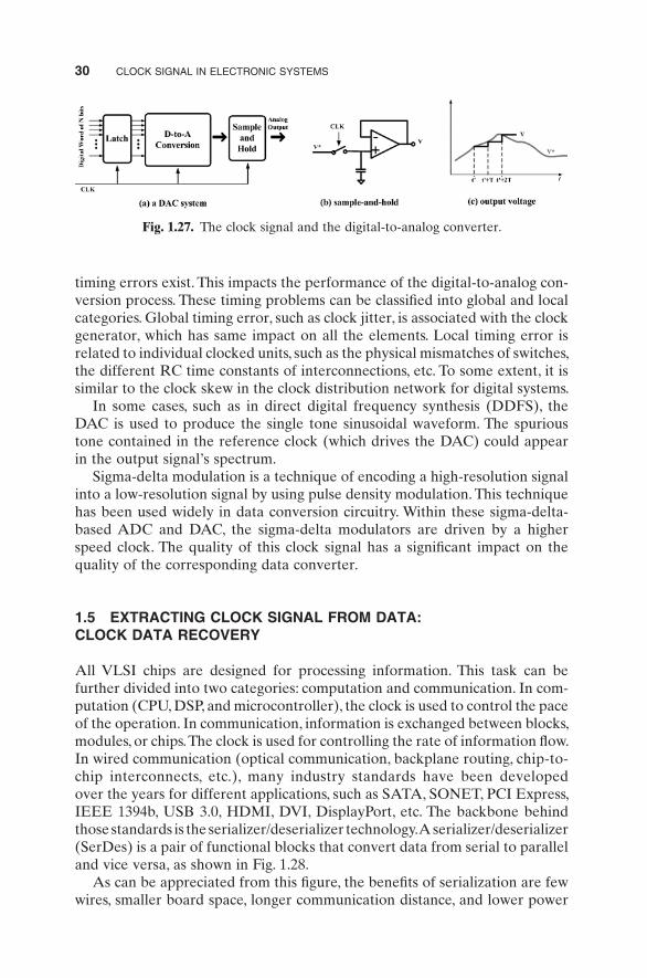
As shown in Fig. 1.21 , the ability to convert a digital signal back to analog is also very important. The digital - to - analog conversion process is essentially the inverse of the analog - to - digital process. There are various types of DACs: current - scaling DAC, voltage - scaling DAC, charge - scaling DAC, and serial DAC. A generic DAC block diagram, which is the representative of all the types, is depicted in Fig. 1.27 . As shown, the clock signal plays a crucial role in the DAC as well: the digital word is synchronously clocked and the analog output is sampled and held by the clock.
Just as in the case of the ADC, one of the fundamental problems in the DAC is the timing accuracy of the conversion. For an N - bit discrete - time signal to be converted into a continuous - time signal, usually 2 N − 1 equally designed elements (current sources) are required. These current sources are switched on and off depending on the input data. Ideally, the switched element shall all turn on/off at the same moment as defi ned by the clock edge. But in reality,

Fig
. 1.2
6. T
he s
purs
are
alia
sed
back
in t
he F
FT
plo
t.
29
30 CLOCK SIGNAL IN ELECTRONIC SYSTEMS
timing errors exist. This impacts the performance of the digital - to - analog con-version process. These timing problems can be classifi ed into global and local categories. Global timing error, such as clock jitter, is associated with the clock generator, which has same impact on all the elements. Local timing error is related to individual clocked units, such as the physical mismatches of switches, the different RC time constants of interconnections, etc. To some extent, it is similar to the clock skew in the clock distribution network for digital systems.
In some cases, such as in direct digital frequency synthesis (DDFS), the DAC is used to produce the single tone sinusoidal waveform. The spurious tone contained in the reference clock (which drives the DAC) could appear in the output signal ’ s spectrum.
Sigma - delta modulation is a technique of encoding a high - resolution signal into a low - resolution signal by using pulse density modulation. This technique has been used widely in data conversion circuitry. Within these sigma - delta - based ADC and DAC, the sigma - delta modulators are driven by a higher speed clock. The quality of this clock signal has a signifi cant impact on the quality of the corresponding data converter.
1.5 EXTRACTING CLOCK SIGNAL FROM DATA: CLOCK DATA RECOVERY
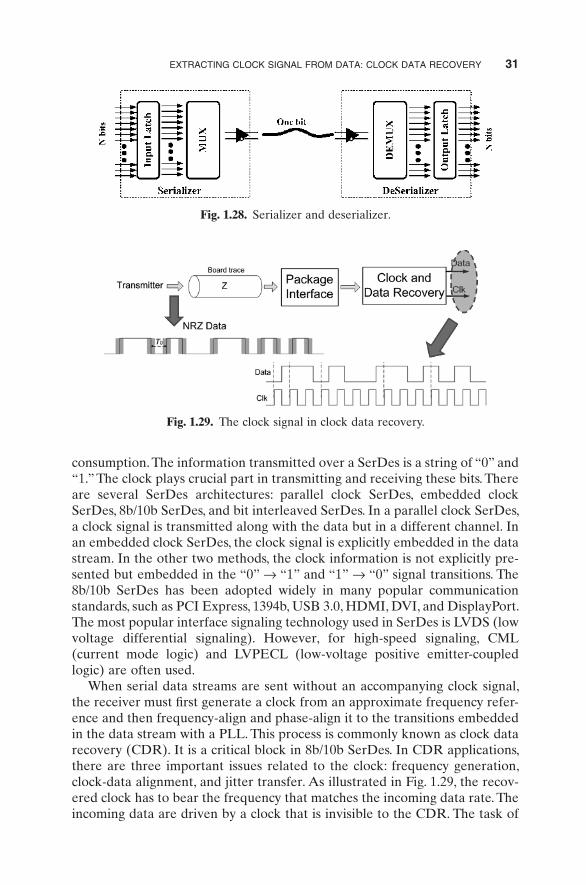
All VLSI chips are designed for processing information. This task can be further divided into two categories: computation and communication. In com-putation (CPU, DSP, and microcontroller), the clock is used to control the pace of the operation. In communication, information is exchanged between blocks, modules, or chips. The clock is used for controlling the rate of information fl ow. In wired communication (optical communication, backplane routing, chip - to - chip interconnects, etc.), many industry standards have been devel oped over the years for different applications, such as SATA, SONET, PCI Express, IEEE 1394b, USB 3.0, HDMI, DVI, DisplayPort, etc. The backbone behind those standards is the serializer/deserializer technology. A serializer/deserializer ( SerDes ) is a pair of functional blocks that convert data from serial to parallel and vice versa, as shown in Fig. 1.28 .
As can be appreciated from this fi gure, the benefi ts of serialization are few wires, smaller board space, longer communication distance, and lower power
Fig. 1.27. The clock signal and the digital - to - analog converter.
EXTRACTING CLOCK SIGNAL FROM DATA: CLOCK DATA RECOVERY 31
Fig. 1.28. Serializer and deserializer.
consumption. The information transmitted over a SerDes is a string of “ 0 ” and “ 1. ” The clock plays crucial part in transmitting and receiving these bits. There are several SerDes architectures: parallel clock SerDes, embedded clock SerDes, 8b/10b SerDes, and bit interleaved SerDes. In a parallel clock SerDes, a clock signal is transmitted along with the data but in a different channel. In an embedded clock SerDes, the clock signal is explicitly embedded in the data stream. In the other two methods, the clock information is not explicitly pre-sented but embedded in the “ 0 ” → “ 1 ” and “ 1 ” → “ 0 ” signal transitions. The 8b/10b SerDes has been adopted widely in many popular communication standards, such as PCI Express, 1394b, USB 3.0, HDMI, DVI, and DisplayPort. The most popular interface signaling technology used in SerDes is LVDS ( low voltage differential signaling ). However, for high - speed signaling, CML ( current mode logic ) and LVPECL ( low - voltage positive emitter - coupled logic ) are often used.
When serial data streams are sent without an accompanying clock signal, the receiver must fi rst generate a clock from an approximate frequency refer-ence and then frequency - align and phase - align it to the transitions embedded in the data stream with a PLL. This process is commonly known as clock data recovery (CDR). It is a critical block in 8b/10b SerDes. In CDR applications, there are three important issues related to the clock: frequency generation, clock - data alignment, and jitter transfer. As illustrated in Fig. 1.29 , the recov-ered clock has to bear the frequency that matches the incoming data rate. The incoming data are driven by a clock that is invisible to the CDR. The task of
Fig. 1.29. The clock signal in clock data recovery.
32 CLOCK SIGNAL IN ELECTRONIC SYSTEMS
the CDR is to fi nd its frequency through received data. Additionally, the phase of this clock has to lie in the center of the data time window for a maximum safety margin. Furthermore, in the process of clock generation, the timing jitter embedded in the incoming data has to be rejected as much as possible.
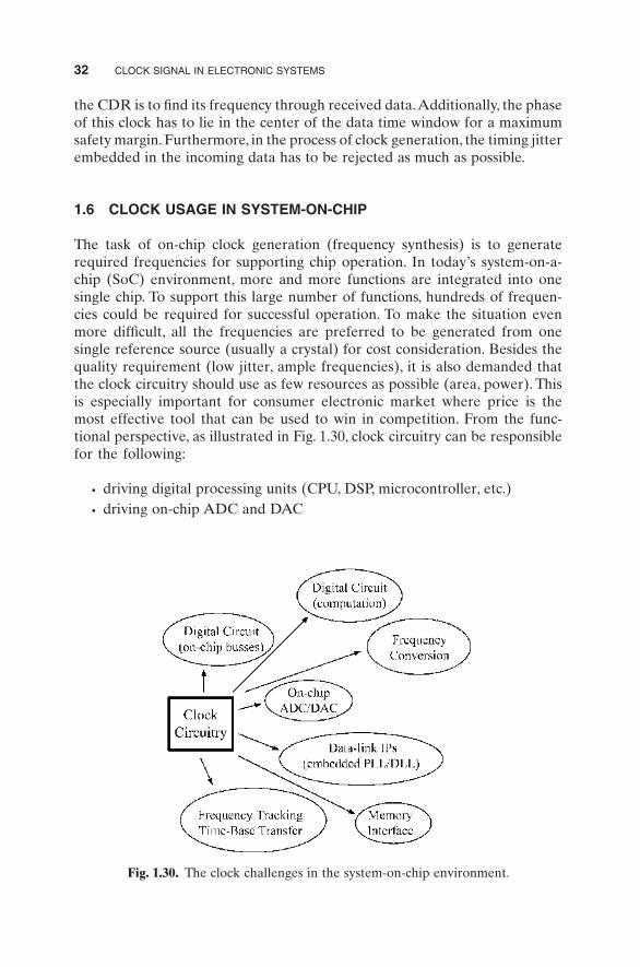
1.6 CLOCK USAGE IN SYSTEM - ON - CHIP
The task of on - chip clock generation (frequency synthesis) is to generate required frequencies for supporting chip operation. In today ’ s system - on - a - chip (SoC) environment, more and more functions are integrated into one single chip. To support this large number of functions, hundreds of frequen-cies could be required for successful operation. To make the situation even more diffi cult, all the frequencies are preferred to be generated from one single reference source (usually a crystal) for cost consideration. Besides the quality requirement (low jitter, ample frequencies), it is also demanded that the clock circuitry should use as few resources as possible (area, power). This is especially important for consumer electronic market where price is the most effective tool that can be used to win in competition. From the func-tional perspective, as illustrated in Fig. 1.30 , clock circuitry can be responsible for the following:
• driving digital processing units (CPU, DSP, microcontroller, etc.) • driving on - chip ADC and DAC
Fig. 1.30. The clock challenges in the system - on - chip environment.
TWO FIELDS: CLOCK GENERATION AND CLOCK DISTRIBUTION 33
• providing frequency reference for on - chip IPs (USB, DDR, LVDS, HDMI, etc.)
• local oscillator ( LO ) for frequency down - conversion or up - conversion • frequency tracking
Overall, digital circuits account for the majority of SoC clock loading. The most important concerns in this task are jitter and skew. On the other hand, the tasks of driving ADC/DAC, providing references to IP addresses, and performing frequency conversions require spectral purity in the clock signal. When clock circuitry is used for frequency tracking (also called time - based transfer or timing recovery), the desirable frequency is not predetermined, but only decided in real time from tracking certain target.
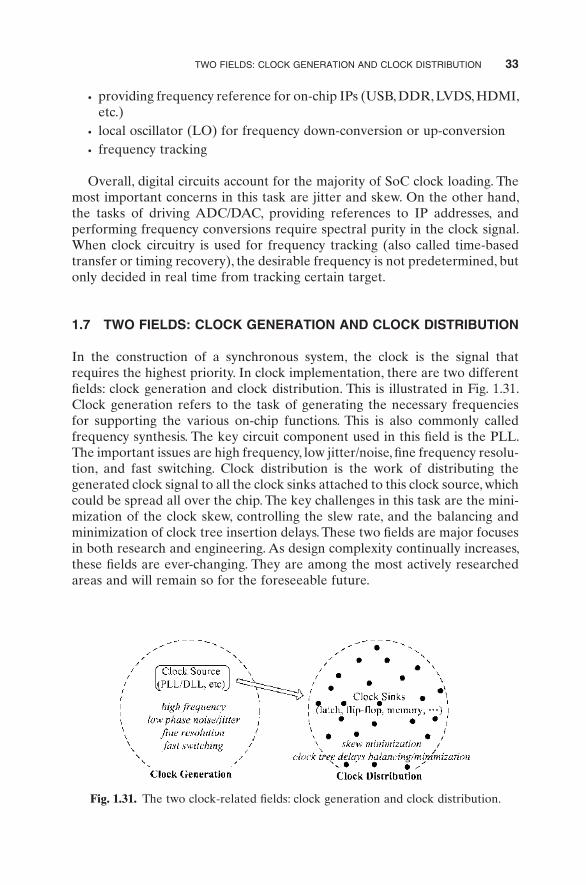
1.7 TWO FIELDS: CLOCK GENERATION AND CLOCK DISTRIBUTION
In the construction of a synchronous system, the clock is the signal that requires the highest priority. In clock implementation, there are two different fi elds: clock generation and clock distribution. This is illustrated in Fig. 1.31 . Clock generation refers to the task of generating the necessary frequencies for supporting the various on - chip functions. This is also commonly called frequency synthesis. The key circuit component used in this fi eld is the PLL. The important issues are high frequency, low jitter/noise, fi ne frequency resolu-tion, and fast switching. Clock distribution is the work of distributing the generated clock signal to all the clock sinks attached to this clock source, which could be spread all over the chip. The key challenges in this task are the mini-mization of the clock skew, controlling the slew rate, and the balancing and minimization of clock tree insertion delays. These two fi elds are major focuses in both research and engineering. As design complexity continually increases, these fi elds are ever - changing. They are among the most actively researched areas and will remain so for the foreseeable future.
Fig. 1.31. The two clock - related fi elds: clock generation and clock distribution.

34 CLOCK SIGNAL IN ELECTRONIC SYSTEMS
BIBLIOGRAPHY
Phase Noise and Jitter
Abidi , A. A. 2006 . “ Phase Noise and Jitter in CMOS Ring Oscillators , ” Solid - State Circuits IEEE J. , vol. 41 , no. 8 , pp. 1803 – 1816 .
Blakkan , K. and M. Soma . 2009 . “ A Time Domain Method to Measure Oscillator Phase Noise , ” VLSI Test Symposium, 2009. VTS ’ 09. 27th IEEE , 3 – 7 May, pp. 297 – 302 .
Chin , J. and A. Cantoni . 1998 . “ Phase Jitter = Timing Jitter? ” Commun. Lett. IEEE , vol. 2 , no. 2 , pp. 54 – 56 .
Demir , A. 2002 . “ Phase Noise and Timing Jitter in Oscillators with Colored - Noise Sources , ” Circuits Syst. I Regular Papers IEEE Trans. , vol. 49 , no. 12 , pp. 1782 – 1791 .
Demir , A. 2006 . “ Computing Timing Jitter from Phase Noise Spectra for Oscillators and Phase - Locked Loops with White and 1/f Noise , ” Circuits Syst. I Regular Papers IEEE Trans. , vol. 53 , no. 9 , pp. 1869 – 1884 .
Hajimiri , A. and T. H. Lee . 1998 . “ General Theory of Phase Noise in Electrical Oscil-lators , ” Solid - State Circuits IEEE J. , vol. 33 , no. 2 , pp. 179 – 194 .
Kim , Y. W. and J. D. Yu . 2008 . “ Phase Noise Model of Single Loop Frequency Synthe-sizer , ” Broadcast. IEEE Trans. , vol. 54 , no. 1 , pp. 112 – 119 .
Kundert , K. S. 1999 . “ Introduction to RF Simulation and Its Application , ” IEEE J. Solid - State Circuits , vol. 34 , pp. 1298 – 1319 .
Kundert , K. S. “ Predicting the Phase Noise and Jitter of PLL - Based Frequency Synthe-sizers, ” http://www.designers - guide.com .
Lecroy . “ Clock Recovery Methods for Jitter Analysis , ” Technical brief. Lee , T. H. and A. Hajimiri . 2000 . “ Oscillator Phase Noise: A Tutorial , ” Solid - State Cir-
cuits IEEE J. , vol. 35 , no. 3 , pp. 326 – 336 . Liang , D. and R. Harjani . 2000 . “ Comparison and Analysis of Phase Noise in Ring
Oscillators , ” Circuits and Systems, 2000. Proceedings. ISCAS 2000 Geneva. The 2000 IEEE International Symposium on , vol. 5 , 28 – 31 May, pp. 77 – 80 .
Liang , D. and R. Harjani . 2002 . “ Design of Low - Phase - Noise CMOS Ring Oscillators , ” Circuits Syst. II Analog Digit. Signal Processing IEEE Trans. , vol. 49 , no. 5 , pp. 328 – 338 .
Navid , R. , T. H. Lee , and R. W. Dutton . 2005 . “ Minimum Achievable Phase Noise of RC Oscillators , ” Solid - State Circuits IEEE J. , vol. 40 , no. 3 , pp. 630 – 637 .
Mak , T. M. 2008 . “ Jitters in High Performance Microprocessors , ” Test Conference, 2008. ITC 2008. IEEE International , 28 – 30 Oct., pp. 1 – 6 .
Poore , R. 2001 . “ Overview on Phase Noise and Jitter, ” Agilent Technologies, http://cp.literature.agilent.com/litweb/pdf/5990 - 3108EN.pdf .
Razavi , B. 1996 . “ A Study of Phase Noise in CMOS Oscillators , ” Solid - State Circuits IEEE J. , vol. 31 , no. 3 , pp. 331 – 343 .
Shimanouchi , M. 2001 . “ An Approach to Consistent Jitter Modeling for Various Jitter Aspects and Measurement Methods , ” Test Conference, 2001, Proceedings, Interna-tional , pp. 848 – 857 .
Tektronix . “ Understanding and Characterizing Timing Jitter , ” application note.
BIBLIOGRAPHY 35
Clock Distribution and Clock Skew
Friedman , E. G. 2001 . “ Clock Distribution Networks in Synchronous Digital Integrated Circuits , ” Proc. IEEE , vol. 89 , no. 5 , pp. 665 – 692 .
Harris , D. , M. Horowitz , and D. Liu . 1999 . “ Timing Analysis including Clock Skew , ” IEEE Trans. CAD , vol. 18 , no. 11 , pp. 1608 – 1618 .
Jiang , X. and S. Horiguchi . 2001 . “ Statistical Skew Modeling for General Clock Distri-bution Networks in Presence of Process Variations , ” IEEE Trans. VLSI Syst. , vol. 9 , no. 5 , pp. 704 – 717 .
Ramanathan , P. , A. J. Dupont , and K. G. Shin . 1994 . “ Clock Distribution in General VLSI Circuits , ” Circuits Syst. I Fundam. Theory Appl. IEEE Trans. , vol. 41 , no. 5 , pp. 395 – 404 .
Zanella , S. , A. Nardi , A. Neviani , M. Quarantelli , S. Saxena , and C. Guardiani . 2000 . “ Analysis of the Impact of Process Variations on Clock Skew , ” Semicond. Manuf. IEEE Trans. , vol. 13 , no. 4 , pp. 401 – 407 .
Clock Jitter on Data Converter
Analog Devices . “ Fundamentals of Sampled Data Systems , ” Application Note, AN - 282.
Angrisani , L. and M. D ’ Arco . 2009 . “ Modeling Timing Jitter Effects in Digital - to - Analog Converters , ” Instrum. Meas. IEEE Trans. , vol. 58 , no. 2 , pp. 330 – 336 .
Brannon , B. “ Sampled System and the Effects of Clock Phase Noise and Jitter , ” Analog Device, AN - 756.
Brannon , B. and A. Barlow . “ Aperture Uncertainty and ADC System Performance , ” Analog Device, AN - 501.
Da Dait , N. , M. Harteneck , C. Sandner , and A. Wiesbauer . 2001 . “ Numerical Modeling of PLL Jitter and the Impact of Its Non - white Spectrum on the SNR of Sampled Signals , ” Mixed - Signal Design, 2001. SSMSD. 2001 Southwest Symposium on , 25 – 27 Feb., pp. 38 – 44 .
Da Dalt , N. , M. Harteneck , C. Sandner , and A. Wiesbauer . 2002 . “ On the Jitter Require-ments of the Sampling Clock for Analog - to - Digital Converters , ” Circuits Syst. I Fundam. Theory Appl. IEEE Trans. , vol. 49 , no. 9 , pp. 1354 – 1360 .
Doris , K. , A. van Roermund , and D. Leenaerts . 2002 . “ A General Analysis on the Timing Jitter in D/A Converters , ” Circuits and Systems, 2002. ISCAS 2002. IEEE Interna-tional Symposium on , vol. 1 , 26 – 29, May, pp. I - 117 – I - 120 .
Hai , T. , L. Toth , and J. M. Khoury . 1999 . “ Analysis of Timing Jitter in Band Pass Sigma - Delta Modulators , ” Circuits Syst. II Analog Digit. Signal Processing IEEE Trans. , vol. 46 , no. 8 , pp. 991 – 1001 .
Jenq , Y. - C. 1997 . “ Direct Digital Synthesizer with Jittered Clock , ” Instrum. Meas. IEEE Trans. , vol. 46 , no. 3 , pp. 653 – 655 .
Neu , T. 2009 . “ Impact of Sampling - Clock Spurs on ADC Performance , ” Analog Appl. J. , 3 rd , 2009, pp. 5 – 12 . Texas Instruments.
Shinagawa , M. , Y. Akazawa , and T. Wakimoto . 1990 . “ Jitter Analysis of High - Speed Sampling Systems , ” IEEE JSSC , vol. 25 , no. 1 , pp. 220 – 224 .
36 CLOCK SIGNAL IN ELECTRONIC SYSTEMS
Clock and SerDes, CDR
Cho , L. C. , C. Lee , C. C. Hung , and S. I. Liu . 2009 . “ A 33.6 - to - 33.8 Gb/s Burst - Mode CDR in 90 nm CMOS Technology , ” JSSC , vol. 44 , no. 3 , pp. 775 – 783 .
Horowitz , M. , C. K. K. Yang , and S. Sidiropoulous . 1998 . “ High - Speed Electrical Signal-ing: Overview and Limitation , ” IEEE Micro. , vol. 18 , no. 1 , pp. 12 – 14 .
Kim , J. , J. Yang , S. Byun , H. Jun , J. Park , C. S. G. Conroy , and B. Kim . 2005 . “ A Four - Channel 3.125 Gb/s/ch CMOS Serial - Link Transceiver with a Mixed - Mode Adap-tive Equalizer , ” JSSC , vol. 40 , no. 2 , pp. 462 – 471 .
Kim , J. K. , J. Kim , G. Kim , and D. K. Jeong . 2009 . “ A Fully Integrated 0.13 um CMOS 40 - Gb/s Serial Link Transceiver , ” JSSC , vol. 44 , no. 5 , pp. 1510 – 1521 .
Lee , J. , K. S. Kundert , and B. Razavi . 2004 . “ Analysis and Modeling of Bang - Bang Clock and Data Recovery Circuit , ” JSSC , vol. 39 , no. 9 , pp. 1571 – 1580 .
Lewis , D. 2004 . “ SerDes Architecture , ” National Semiconductor Corporation. Loke , A. L. S. , R. K. Barnes , T. T. Wee , M. M. Oshima , C. E. Moore , R. R. Kennedy , and
M. J. Gilsdorf . 2006 . “ A Versatile 90 nm Charge - Pump PLL for SerDes Transmitter Clocking , ” JSSC , vol. 41 , no. 8 , pp. 1894 – 1907 .
“ LVDS Owner ’ s Manual Design Guide , ” 2001 . National Semiconductor Corporation. Razavi , B. 2002 . “ Challenges in the Design of High - Speed Clock and Data Clock Data
Recovery Circuits , ” IEEE Communication Magazine , Aug..
Time - Average - Frequency and Digital - to - Frequency Converter
Xiu , L. 2008a . “ The Concept of Time - Average - Frequency and Mathematical Analysis of Flying - Adder Frequency Synthesis Architecture , ” IEEE Circuit And System Magazine , 3rd quarter, pp. 27 – 51 , Sep..
Xiu , L. 2008b . “ Some Open Issues Associated with the New Type of Component: Digital - to - Frequency Converter , ” IEEE Circuit And System Magazine , 3rd quarter, pp. 90 – 84 , Sep..