clc425 ultra low noise wideband op amp · miscellaneous performance clc425 ... in order to cancel...
TRANSCRIPT

CLC425Ultra Low Noise Wideband Op AmpGeneral DescriptionThe CLC425 combines a wide bandwidth (1.9GBW) with avery low input noise (1.05nV/ , 1.6pA/ ) and low dcerrors (100µV VOS, 2µV/˚C drift) to provide a very precise,wide dynamic range op amp offering closed-loop gains of≥10.
Singularly suited for very wideband high gain operation, theCLC425 employs a traditional voltage feedback topologyproviding all the benefits of balanced inputs, such as lowoffsets and drifts, as well as a 96dB open loop gain, a 100dBCMRR and a 95dB PSRR.
The CLC425 also offers great flexibility with its externallyadjustable supply current, allowing designers to easilychoose the optimum set of power, bandwidth, noise anddistortion performance. Operating from ±5V power supplies,the CLC425 defaults to a 15mA quiescent current, or byadding one external resistor, the supply current can be ad-justed to less than 5mA.
The CLC425’s combination of ultra low noise, wide gainbandwidth, high slew rate and low dc errors will enableapplications in areas such as medical diagnostic ultrasound,magnetic tape & disk storage, communications andopto-electronics to achieve maximum high frequencysignal-to-noise ratios.
Enhanced Solutions (Military/Aerospace)
SMD Number: 5962-93259
Space level versions also available.
For more information, visit http://www.national.com/mil
Featuresn 1.9GHz gain-bandwidth productn 1.05nV/ input voltage noise
n 0.8pA/ @ ICC ≤ 5mAn 100µV input offset voltage, 2µV/˚C driftn 350V/µs slew raten 15mA to 5mA adjustable supply currentn Gain range ±10 to ±1,000V/Vn Evaluation boards & simulation macromodeln 0.9dB NF @ Rs = 700Ω
Applicationsn Instrumentation sense amplifiersn Ultrasound pre-ampsn Magnetic tape & disk pre-ampsn Photo diode transimpedance amplifiersn Wide band active filtersn Low noise figure RF amplifiersn Professional audio systemsn Low noise loop filters for PLLs
Equivalent Input Voltage Noise
01270853
Connection Diagrams
01270851
PinoutSOT23-5
01270852
PinoutDIP & SOIC
May 2001C
LC425
Ultra
LowN
oiseW
idebandO
pA
mp
© 2001 National Semiconductor Corporation DS012708 www.national.com
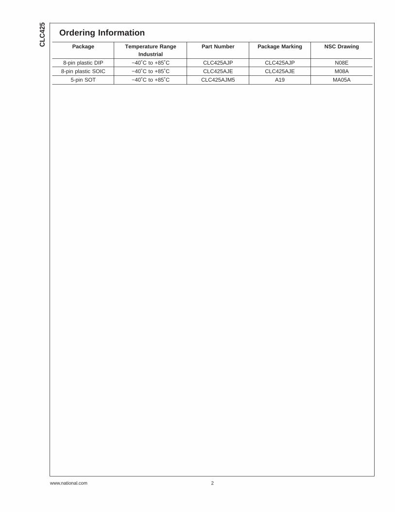
Ordering Information
Package Temperature RangeIndustrial
Part Number Package Marking NSC Drawing
8-pin plastic DIP −40˚C to +85˚C CLC425AJP CLC425AJP N08E
8-pin plastic SOIC −40˚C to +85˚C CLC425AJE CLC425AJE M08A
5-pin SOT −40˚C to +85˚C CLC425AJM5 A19 MA05A
CLC
425
www.national.com 2

Absolute Maximum Ratings (Note 1)
If Military/Aerospace specified devices are required,please contact the National Semiconductor Sales Office/Distributors for availability and specifications.
Supply Voltage (VCC) ±7V
IOUT
Output is short circuit protected toground, but maximum reliability willbe maintained if IOUT does notexceed... 125mA
Common Mode Input Voltage ±VCC
Maximum Junction Temperature +150˚C
Operating Temperature Range −40˚C to +85˚C
Storage Temperature Range −65˚C to +150˚C
Lead Solder Duration (+300˚C) 10 sec
ESD rating (human body model) 1000V
Operation RatingsThermal Resistance
Package (θJC) (θJA)
MDIP 70˚C/W 125˚C/W
SOIC 65˚C/W 145˚C/W
SOT-23 115˚C/W 185˚C/W
Electrical CharacteristicsAV= +20, VCC = ±5V, Rg = 26.1Ω, RL = 100Ω, Rf = 499Ω; unless specified
Symbol Parameter Conditions Typ Min/Max (Note 2) Units
Ambient Temperature CLC425AJ +25˚C −40˚C +25˚C +85˚
Frequency Domain Response
GBW Gain Bandwidth Product VOUT < 0.4VPP 1.9 1.5 1.5 1.0 GHz
SSBW -3dB Bandwidth VOUT < 0.4VPP 95 75 75 50 MHz
LSBW VOUT < 5.0VPP 40 30 30 20 MHz
Gain Flatness VOUT< 0.4VPP
GFP Peaking DC to 30MHz 0.3 0.7 0.5 0.7 dB
GFR Rolloff DC to 30MHz 0.1 0.7 0.5 0.7 dB
LPD Linear Phase Deviation DC to 30MHz 0.7 1.5 1.5 2.5 deg
Time Domain Response
TRS Rise and Fall Time 0.4V Step 3.7 4.7 4.7 7.0 ns
TSS Settling Time to 0.2% 2V Step 22 30 30 40 ns
OS Overshoot 0.4V Step 5 12 10 12 %
SR SlewRate 2V Step 350 250 250 200 V/µs
Distortion And Noise Response
HD2 2nd Harmonic Distortion 1VPP, 10MHz −53 48 48 46 dBc
HD3 3rd Harmonic Distortion 1VPP, 10MHz −75 65 65 60 dBc
IMD 3rd Order IntermodulationIntercept
10MHz 35 dBm
Equivalent Input Noise
VN Voltage 1MHz to 100MHz 1.05 1.25 1.25 1.8 nV/
ICN Current 1MHz to 100MHz 1.6 4.0 2.5 2.5 pA/
NF Noise Figure Rs = 700Ω 0.9 dB
Static, DC Performance
AOL Open Loop Gain DC 96 77 86 86 dB
VIO Input Offset Voltage (Note 3) ±100 ±1000 ±800 ±1000 µV
DVIO Average Drift ±2 8 - 4 µV/˚C
IB Input Bias Current (Note 3) Non-Inverting 12 40 20 20 µA
DIB Average Drift −100 −250 - −120 nA/˚C
IIO Input Offset Current ±0.2 3.4 2.0 2.0 µA
DIIO Average Drift ±3 ±50 - ±25 nA/C˚
PSRR Power Supply Rejection Ratio DC 95 82 88 86 dB
CMRR Common Mode Rejection Ratio DC 100 88 92 90 dB
ICC Supply Current (Note 3) RL = ∞ 15 18 16 16 mA
Miscellaneous Performance
CLC
425
www.national.com3

Electrical Characteristics (Continued)AV= +20, VCC = ±5V, Rg = 26.1Ω, RL = 100Ω, Rf = 499Ω; unless specified
Symbol Parameter Conditions Typ Min/Max (Note 2) Units
RINC Input Resistance Common-Mode 2 0.6 1.6 1.6 MΩRIND Differential-Mode 6 1 3 3 kΩCINC Input Capacitance Common-Mode 1.5 2 2 2 pF
CIND Differential-Mode 1.9 3 3 3 pF
ROUT Output Resistance Closed Loop 5 50 10 10 mΩVO Output Voltage Range RL = ∞ ±3.8 ±3.5 ±3.7 ±3.7 V
VOL RL = 100Ω ±3.4 ±2.8 ±3.2 ±3.2 V
CMIR Input Voltage Range Common Mode ±3.8 ±3.4 ±3.5 ±3.5 V
IOP Output Current Source 80 70 70 70 mA
ION Sink 90 45 55 55 mA
Note 1: “Absolute Maximum Ratings” are those values beyond which the safety of the device cannot be guaranteed. They are not meant to imply that the devicesshould be operated at these limits. The table of “Electrical Characteristics” specifies conditions of device operation.
Note 2: Max/min ratings are based on product characterization and simulation. Individual parameters are tested as noted. Outgoing quality levels are determinedfrom tested parameters.
Note 3: AJ-level: spec. is 100% tested at +25˚C, sample at 85˚C.
CLC
425
www.national.com 4

Typical Performance CharacteristicsNon-Inverting Frequency Response Inverting Frequency Response
01270801 01270802
Frequency Response vs. I CC (AV = +20) Open Loop Gain and Phase vs. I CC
01270803
01270804
Open Loop Gain and Phase vs. R L Open Loop Gain and Phase vs. Temp
01270805 01270806
CLC
425
www.national.com5

Typical Performance Characteristics (Continued)
Non-Inverting Response (I CC = 5.0mA) Frequency Response for Various R Ls
01270807
01270808
Gain Flatness & Linear Phase Deviation Equivalent Input Noise
01270809 01270810
Maximum Output Swing vs. Frequency Closed-Loop Output Impedance
01270811 01270812
CLC
425
www.national.com 6

Typical Performance Characteristics (Continued)
CMRR vs. Common-Mode Input Voltage Common-Mode Input Transimpedance
0127081301270814
Differential Input Impedance Pulse Response (V O1 = VPP)
01270815
01270816
Large Signal Pulse Response (V O1 = VPP) Settling Time vs. Gain
01270817
01270818
CLC
425
www.national.com7

Typical Performance Characteristics (Continued)
Short Term Settling Time Long Term Settling Time
01270819
01270820
Settling Time vs. C L and RS Supply Current Range vs. R p
01270821 01270822
Gain-Bandwidth Product vs. I CC Differential Gain and Phase (4.43MHz)
01270823
01270824
CLC
425
www.national.com 8

Typical Performance Characteristics (Continued)
2nd and 3rd Harmonic Distortion (V O1 = VPP) Distortion vs. Gain & I CC (VO1 = VPP fO = 3MHz)
01270825 01270826
2-Tone, 3rd Order Intermodulation Intercept Output Voltage vs. Load
01270827 01270828
CMRR and PSRR Typical DC Errors vs. Temperature
01270829
01270830
CLC
425
www.national.com9

Application Division
Introduction
The CLC425 is a very wide gain bandwidth, ultra low noisevoltage feedback operational amplifier which enables appli-cation areas such as medical diagnostic ultrasound, mag-netic tape & disk storage and fiber-optics to achieve maxi-mum high frequency signal-to-noise ratios. The set ofcharacteristic plots located in the “Typical Performance” sec-tion illustrates many of the performance trade offs. Thefollowing discussion will enable the proper selection of ex-ternal components in order to achieve optimum device per-formance.
Bias Current Cancellation
In order to cancel the bias current errors of the non-invertingconfiguration, the parallel combination of the gain setting(Rg) and feedback (Rf) resistors should equal the equivalentsource resistance (Rseq) as defined in Figure 1. Combiningthis constraint with the non-inverting gain equation also seenin Figure 1, allows both Rf and Rg to be determined explicitlyfrom the following equations:
Rf = AVRseq and Rg = Rf/(AV−1).
When driven from a 0Ω source, such as that from the outputof an op amp, the non-inverting input of the CLC425 shouldbe isolated with at least a 25Ω series resistor.
As seen in Figure 2, bias current cancellation is accom-plished for the inverting configuration by placing a resistor(Rb) on the non-inverting input equal in value to the resis-tance seen by the inverting input (Rf\(Rg+s)). Rb is recom-mended to be no less than 25Ω for best CLC425 perfor-mance. The additional noise contribution of Rb can beminimized through the use of a shunt capacitor.
Total Input Noise vs. Source Resistance
In order to determine maximum signal-to-noise ratios fromthe CLC425, an understanding of the interaction betweenthe amplifier’s intrinsic noise sources and the noise arisingfrom its external resistors is necessary.
describes the noise model for the non-inverting amplifierconfiguration showing all noise sources. In addition to theintrinsic input voltage noise (en) and current noise (in = in+ =in−) sources, there also exists thermal voltage noise
(et = 4kTR)
associated with each of the external resistors. Equation 1provides the general form for total equivalent input voltagenoise density (eni). Equation 2 is a simplification of Equation1 that assumes
(1)
Rf\Rg=Rseq for bias current cancellation. Figure 4 illustratesthe equivalent noise model using this assumption. Figure 5is a plot of eni against equivalent source resistance (Rseq)with all of the contributing voltage noise source of Equation 2shown. This plot gives the expected eni for a given (Rseq)which assumes Rf\Rg=Rseq for bias current cancellation.The total equivalent output voltage noise (en0) is eni*Av.
01270831
FIGURE 1. Non-Inverting Amplifier Configuration
01270834
FIGURE 2. Inverting Amplifier Configuration
01270832
FIGURE 3. Non-inverting Amplifier Noise Model
CLC
425
www.national.com 10

Application Division (Continued)
(2)
As seen in Figure 5, eni is dominated by the intrinsic voltagenoise (en) of the amplifier for equivalent source resistancesbelow 33.5Ω. Between 33.5Ω and 6.43kΩ, eni is dominatedby the thermal noise (et= 4kTRseq) of the externalresistor. Above 6.43kΩ, eni is dominated by the amplifier’scurrent noise ( 2inRseq). The point at which theCLC425’s voltage noise and current noise contribute equallyoccurs for Rseq=464Ω (i.e., en/ 2in). As an example,configured with a gain of +20V/V giving a -3dB of 90MHz anddriven from an Rseq=25Ω, the CLC425 produces a totalequivalent input noise voltage (eni x 1.57*90MHz) of16.5µVrms.
If bias current cancellation is not a requirement, then Rf\Rg
does not need to equal Rseq. In this case, according toEquation 1, RfRg should be as low as possible in order tominimize noise. Results similar to Equation 1 are obtainedfor the inverting configuration of Figure 2 if Rseq is replacedby Rb and Rg is replaced by Rg+Rs. With these substitutions,Equation 1 will yield an eni referred to the non-inverting input.Referring eni to the inverting input is easily accomplished bymultiplying eni by the ratio of non-inverting to inverting gains.
Noise Figure
Noise Figure (NF) is a measure of the noise degradationcaused by an amplifier.
(3)
The Noise Figure formula is shown in Equation 3. The addi-tion of a terminating resistor RT, reduces the external ther-mal noise but increases the resulting NF. The NF is in-creased because RT reduces the input signal amplitude thusreducing the input SNR.
(4)
The noise figure is related to the equivalent source resis-tance (Rseq) and the parallel combination of Rf and Rg. Tominimize noise figure, the following steps are recommended:
• Minimize Rf\Rg
• Choose the Optimum RS (OPT)
ROPT is the point at which the NF curve reaches a minimumand is approximated by:
ROPT )en/inFigure 6 is a plot of NF vs Rs with RfRg=9.09(Av=+10). TheNF curves for both Unterminated and Terminated systemsare shown. The Terminated curve assumes Rs=RT. Thetable indicates the NF for various source resistances includ-ing Rs=ROPT.
Supply Current Adjustment
The CLC425’s supply current can be externally adjusteddownward from its nominal value by adding an optionalresistor (Rp) between pin 8 and the negative supply asshown in Figure 7. Several of the plots found within the plotpages demonstrate the CLC425’s behavior at different sup-ply currents. The plot labeled “Icc vs Rp” provides the meansfor selecting Rp and shows the results of standard IC pro-cess variation which is bounded by the 25˚C curve.
01270835
FIGURE 4. Noise Model with R f||Rg = Rseq
01270836
FIGURE 5. Voltage Noise Density vs. SourceResistance
01270837
FIGURE 6. Noise Figure vs. Source Resistance
CLC
425
www.national.com11

Application Division (Continued)
Non-Inverting Gains Less Than 10V/V
Using the CLC425 at lower non-inverting gains requiresexternal compensation such as the shunt compensation asshown in Figure 8. The quiescent supply current must alsobe reduced to 5mA with Rp for stability. The compensationcapacitors are chosen to reduce frequency response peak-ing to less than 1dB. The plot in the “Typical Performance”section labeled “differential gain and Phase” shows the videoperformance of the CLC425 with this compensation circuitry.
Inverting Gains Less Than 10V/V
The lag compensation of Figure 9 will achieve stability forlower gains. Placing the network between the two inputterminals does not affect the closed-loop nor noise gain, butis best used for the inverting configuration because of itsaffect on the non-inverting input impedance.
Single-Supply Operation
The CLC425 can be operated with single power supply asshown in Figure 10. Both the input and output are capaci-tively coupled to set the dc operating point.
Low Noise Transimpedance Amplifier
The circuit of Figure 11 implements a low-noise transimped-ance amplifier commonly used with photo-diodes. The tran-simpedance gain is set by Rf. The simulated frequencyresponse is shown in Figure 12 and shows the influence Cf
has over gain flatness. Equation 4 provides the total inputcurrent noise density (ini) equation for the basic transimped-ance configuration and is plotted against feedback resis-tance (Rf) showing all contributing noise sources in Figure13. This plot indicates the expected total equivalent inputcurrent noise density (ini) for a given feedback resistance(Rf). The total equivalent output voltage noise density (eno) isini*Rf.
01270838
FIGURE 7. External Supply Current Adjustment
01270839
FIGURE 8. External Shunt Compensation
01270841
FIGURE 9. External Lag Compensation
01270843
FIGURE 10. Single Supply Operation
CLC
425
www.national.com 12

Application Division (Continued)
(5)
Very Low Figure Amplifier
The circuit of Figure 14 implements a very low Noise Figureamplifier using a step-up transformer combined with aCLC425 and a CLC404. The circuit is configured with a gainof 35.6dB. The circuit achieves measured Noise Figures ofless than 2.5dB in the 10-40MHz region, 3rd order interceptsexceed +30dB for frequencies less than 40MHz and gainflatness of 0.5dB is measured in the 1-50MHz passbands.Application Note OA-14 provides greater detail on these lowNoise Figure techniques.
Low Noise Integrator
The CLC425 implements a deBoo integrator shown in Figure15. Integration linearity is maintained through positive feed-back. The CLC425’s low input offset voltage and matchedinputs allowing bias current cancellation provide for veryprecise integration. Stability is maintained through the con-straint on the circuit elements.
High-Gain Sallen-Key Active Filters
The CLC425 is well suited for high gain Sallen-Key type ofactive filters. Figure 16 shows the 2ndorder Sallen-Key lowpass filter topology. Using component predistortion methodsas discussed in OA-21 enables the proper selection of com-ponents for these high-frequency filters.
01270840
FIGURE 11. Transimpedance Amplifier Configuration
01270842
FIGURE 12. Transimpedance Amplifier FrequencyResponse
01270844
FIGURE 13. Current Noise Density vs. FeedbackResistance
01270846
FIGURE 14. Very Noise Figure Amplifier
01270848
FIGURE 15. Low Noise Integrator
CLC
425
www.national.com13
Application Division (Continued)
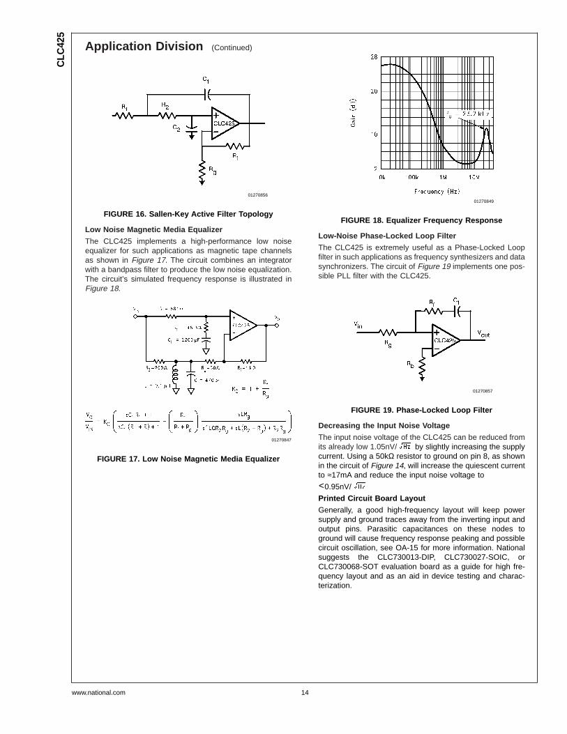
Low Noise Magnetic Media Equalizer
The CLC425 implements a high-performance low noiseequalizer for such applications as magnetic tape channelsas shown in Figure 17. The circuit combines an integratorwith a bandpass filter to produce the low noise equalization.The circuit’s simulated frequency response is illustrated inFigure 18.
Low-Noise Phase-Locked Loop Filter
The CLC425 is extremely useful as a Phase-Locked Loopfilter in such applications as frequency synthesizers and datasynchronizers. The circuit of Figure 19 implements one pos-sible PLL filter with the CLC425.
Decreasing the Input Noise Voltage
The input noise voltage of the CLC425 can be reduced fromits already low 1.05nV/ by slightly increasing the supplycurrent. Using a 50kΩ resistor to ground on pin 8, as shownin the circuit of Figure 14, will increase the quiescent currentto ≈17mA and reduce the input noise voltage to<0.95nV/
Printed Circuit Board Layout
Generally, a good high-frequency layout will keep powersupply and ground traces away from the inverting input andoutput pins. Parasitic capacitances on these nodes toground will cause frequency response peaking and possiblecircuit oscillation, see OA-15 for more information. Nationalsuggests the CLC730013-DIP, CLC730027-SOIC, orCLC730068-SOT evaluation board as a guide for high fre-quency layout and as an aid in device testing and charac-terization.
01270856
FIGURE 16. Sallen-Key Active Filter Topology
01270847
FIGURE 17. Low Noise Magnetic Media Equalizer
01270849
FIGURE 18. Equalizer Frequency Response
01270857
FIGURE 19. Phase-Locked Loop Filter
CLC
425
www.national.com 14

Physical Dimensions inches (millimeters)unless otherwise noted
8-Pin SOICNS Package Number M08A
8-Pin MDIPNS Package Number N08E
CLC
425
www.national.com15

Physical Dimensions inches (millimeters) unless otherwise noted (Continued)
5-Pin SOT23NS Package Number MA05A
LIFE SUPPORT POLICY
NATIONAL’S PRODUCTS ARE NOT AUTHORIZED FOR USE AS CRITICAL COMPONENTS IN LIFE SUPPORTDEVICES OR SYSTEMS WITHOUT THE EXPRESS WRITTEN APPROVAL OF THE PRESIDENT AND GENERALCOUNSEL OF NATIONAL SEMICONDUCTOR CORPORATION. As used herein:
1. Life support devices or systems are devices orsystems which, (a) are intended for surgical implantinto the body, or (b) support or sustain life, andwhose failure to perform when properly used inaccordance with instructions for use provided in thelabeling, can be reasonably expected to result in asignificant injury to the user.
2. A critical component is any component of a lifesupport device or system whose failure to performcan be reasonably expected to cause the failure ofthe life support device or system, or to affect itssafety or effectiveness.
National SemiconductorCorporationAmericasEmail: [email protected]
National SemiconductorEurope
Fax: +49 (0) 180-530 85 86Email: [email protected]
Deutsch Tel: +49 (0) 69 9508 6208English Tel: +44 (0) 870 24 0 2171Français Tel: +33 (0) 1 41 91 8790
National SemiconductorAsia Pacific CustomerResponse GroupTel: 65-2544466Fax: 65-2504466Email: [email protected]
National SemiconductorJapan Ltd.Tel: 81-3-5639-7560Fax: 81-3-5639-7507
www.national.com
CLC
425
Ultr
aLo
wN
oise
Wid
eban
dO
pA
mp
National does not assume any responsibility for use of any circuitry described, no circuit patent licenses are implied and National reserves the right at any time without notice to change said circuitry and specifications.